MAX3421E_cn中文资料
MAX491EESD+中文资料

Driver Input Voltage (DI).............................-0.5V to (VCC + 0.5V)
Driver Output Voltage (Y, Z; A, B) ..........................-8V to +12.5V
Receiver Input Voltage (A, B).................................-8V to +12.5V
元器件交易网
MAX481E/MAX483E/MAX485E/MAX487E–MAX491E/MAX1487E
±15kV ESD-Protected, Slew-Rate-Limited, Low-Power, RS-485/RS-422 Transceivers
ABSOLUTE MAXIMUM RATINGS
General Description
The MAX481E, MAX483E, MAX485E, MAX487E– MAX491E, and MAX1487E are low-power transceivers for RS-485 and RS-422 communications in harsh environments. Each driver output and receiver input is protected against ±15kV electro-static discharge (ESD) shocks, without latchup. These parts contain one driver and one receiver. The MAX483E, MAX487E, MAX488E, and MAX489E feature reduced slew-rate drivers that minimize EMI and reduce reflections caused by improperly terminated cables, thus allowing error-free data transmission up to 250kbps. The driver slew rates of the MAX481E, MAX485E, MAX490E, MAX491E, and MAX1487E are not limited, allowing them to transmit up to 2.5Mbps.
MAX3421E 带SPI接口的USB外设 主机控制器 编程指南
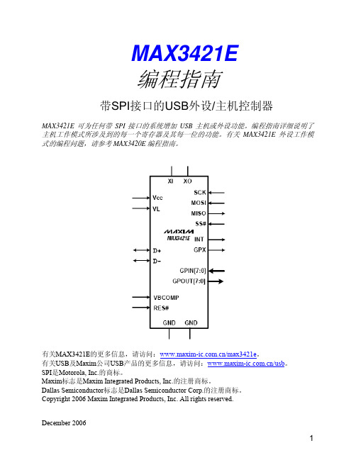
MAX3421E编程指南带SPI接口的USB外设/主机控制器MAX3421E可为任何带SPI接口的系统增加USB主机或外设功能。
编程指南详细说明了主机工作模式所涉及到的每一个寄存器及其每一位的功能。
有关MAX3421E外设工作模式的编程问题,请参考MAX3420E编程指南。
有关MAX3421E的更多信息,请访问:/max3421e。
有关USB及Maxim公司USB产品的更多信息,请访问:/usb。
SPI是Motorola, Inc.的商标。
Maxim标志是Maxim Integrated Products, Inc.的注册商标。
Dallas Semiconductor标志是Dallas Semiconductor Corp.的注册商标。
Copyright 2006 Maxim Integrated Products, Inc. All rights reserved.December 20061关于编程指南MAX3421E是具有双重作用的USB控制器,既可以设置为USB外设,又可设置为主机。
作为外设时,MAX3421E的工作机制与只能作为外设的MAX3420E完全相同。
如果只打算将MAX3421E用作USB外设,可运行现有的MAX3420E代码,并将HOST位置0 (缺省值),编程细节可参考MAX3420E编程指南。
如果只打算将MAX3421E用作USB外设,但又想充分利用MAX3421E新提供的外设特性,请参阅本编程指南中新增的寄存器R21至R24,以及新增的寄存器位PULSEWID1/0、SEPIRQ和HOST的说明,同时参考MAX3420E编程指南。
大多数MAX3421E的用户希望了解主机工作模式的详细编程信息,这也正是编写该指南的目的所在。
因此,列出主机操作所用到的位和寄存器(表1)是理所当然的。
但为了便于参考,表2给出了主机和外设工作模式用到的所有寄存器位。
如果浏览的是电子文档,那么表1可以作为导航工具。
MAX3421EVKIT-1+;中文规格书,Datasheet资料
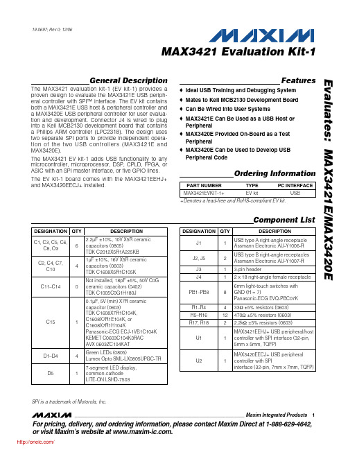
General DescriptionThe MAX3421 evaluation kit-1 (EV kit-1) provides a proven design to evaluate the MAX3421E USB periph-eral controller with SPI™ interface. The EV kit contains both a MAX3421E USB host & peripheral controller and a MAX3420E USB peripheral controller for user evalua-tion and development. Connector J4 is wired to plug into a Keil MCB2130 development board that contains a Philips ARM controller (LPC2318). The design uses two separate SPI ports to provide independent opera-tion of the two USB controllers (MAX3421E and MAX3420E).The MAX3421 EV kit-1 adds USB functionality to any microcontroller, microprocessor, DSP, CPLD, FPGA, or ASIC with an SPI master interface, or five GPIO lines.The EV kit-1 board comes with the MAX3421EEHJ+and MAX3420EECJ+ installed.Features♦Ideal USB Training and Debugging System ♦Mates to Keil MCB2130 Development Board ♦Can Be Wired into User Systems♦MAX3421E Can Be Used as a USB Host or Peripheral ♦MAX3420E Provided On-Board as a Test Peripheral ♦MAX3420E Can be Used to Develop USB Peripheral CodeEvaluates: MAX3421E/MAX3420EMAX3421 Evaluation Kit-1________________________________________________________________Maxim Integrated Products119-0697; Rev 0; 12/06Component ListFor pricing, delivery, and ordering information, please contact Maxim Direct at 1-888-629-4642,or visit Maxim’s website at .Ordering InformationSPI is a trademark of Motorola, Inc.E v a l u a t e s : M A X 3421E /M A X 3420EMAX3421 Evaluation Kit-12_______________________________________________________________________________________Component List (continued)Detailed Descriptionof Hardware The MAX3421 EV kit-1 has three USB connectors (Figure1). The MAX3421E is wired to USB connectors J1 and J2. Plug a cable into USB Type A connector J1 when using the MAX3421E as a host. Plug a cable into USB Type B connector J2 when using the MAX3421E as a peripheral. Do not use J1 and J2 at the same time.Connectors J1 and J2 have their D+ and D- pins wired together, and are intended to be connected only one at a time. USB peripheral controller MAX3420E is wired to USB Type B connector J5.When the MAX3421E (U1) operates as a host, the EV kit must supply V BUS power to USB Type A connector J1. This power must in turn be supplied to the EV kit through power connector J3, which is located in the middle of the board. When mated with a board such as the Keil MCB2130, a “flying lead” can be attached between J3 and the Keil board’s 5V IN test pad. Alternatively, a standard 5VDC lab supply can be used. The MAX4793 (U3) controls and current-limits the V BUS voltage. U1 can turn V BUS power on and off using one of its G P-OUT pins (G POUT7), and can detect a 300mA overcurrent condition on G P-IN pin, (G PIN0). Refer to the MAX4793 data sheet for more information. Buttons and lights are connected to both the MAX3420E and MAX3421E controllers. U1 drives a 7-segment readout and connects to four pushbuttons (PB1–PB4). U2 drives four LEDS and connects to push-buttons PB5–PB8.The MAX3420E and MAX3421E connect to two sepa-rate SPI ports (see Table1). This allows host and peripheral applications to run concurrently in the same code, when implemented on a dual-SPI microcontroller (such as the ARM LPC2318 used on the Keil MCB2130 board). This provides an ideal USB training and debug-ging system. The host can dispatch USB requests to the peripheral, the peripheral can respond, and the host can evaluate the results—all in the same C code.Stand-Alone Operation Although the MAX3421 EV kit-1 is designed to plug into a Keil MCB2130 board, it also functions as a stand-alone board that can be wired into any customer sys-tem with an SPI interface. Table 1 shows the J4 pins that correspond to the MAX3420E and MAX3421E interfaces.Figure1. Block DiagramEvaluates: MAX3421E/MAX3420E MAX3421 Evaluation Kit-1 _______________________________________________________________________________________3User Notes:1)The MAX3420E connects to USB Type B connector J5, while the MAX3421E connects both to USB Type A connector J1 and to USB Type B connector J2.The MAX3421E, therefore, can be connected as a host (J1) or a peripheral (J2).2)The user system must supply 3.3V on J4 pins 1-2 to power the board. The 3.3V supply should be capa-ble of providing 100mA.3)The RES pins connect directly to the MAX3420E/MAX3421E reset pins. It must be driven high for the chip to operate.4)When operating the MAX3421E as a host controller,the user system must provide 5V power on J4 pins 33-34, or on J3 pin 3. This voltage connects to the V BUS pin of USB Type A connector J1 through a current-limiting switch. The user system must supplyenough current to power any USB device plugged into J1. The current-limiting switch (a MAX4793) lim-its the V BUS current to 300mA.5)Keep leads to the target system short (under 6in).Long leads and insufficient grounds can lead to sig-nal ringing and erratic operation.6)When using the MAX3421E as a host, the user program must set the MAX3421E G PO7 pin high to turn on the V BUS switch (U3) that supplies 5V to the USB Type A connector J1. Note that the MAX3421E output port also drives the 7-segment readout using G PO[6:0]. Therefore, the code that updates the 7-segment readout must preserve the bit 7 setting, and the code that turns V BUS on and off must preserve the bits [6:0] settings. This is easi-ly accomplished by first reading the states of the output bits, changing only the needed bits, then writing them back.E v a l u a t e s : M A X 3421E /M A X 3420EMAX3421 Evaluation Kit-14_______________________________________________________________________________________Table 1. J4 Interface to the MAX3420E and MAX3421EFigure2a. MAX3421 EV Kit-1 SchematicMAX3421 Evaluation Kit-1 _______________________________________________________________________________________5Evaluates: MAX3421E/MAX3420EE v a l u a t e s : M A X 3421E /M A X 3420EMAX3421 Evaluation Kit-16_______________________________________________________________________________________Figure 2b. MAX3421 EV Kit-1 SchematicFigure3. MAX3421 EV Kit-1 Component Placement Guide—Component Side Evaluates: MAX3421E/MAX3420E_______________________________________________________________________________________7E v a l u a t e s : M A X 3421E /M A X 3420EMAX3421 Evaluation Kit-18_______________________________________________________________________________________Figure 4. MAX3421 EV Kit-1 PCB Layout—Component SideMaxim cannot assume responsibility for use of any circuitry other than circuitry entirely embodied in a Maxim product. No circuit patent licenses are implied. Maxim reserves the right to change the circuitry and specifications without notice at any time.Maxim Integrated Products, 120 San Gabriel Drive, Sunnyvale, CA 94086 408-737-7600 _____________________9©2006 Maxim Integrated Productsis a registered trademark of Maxim Integrated Products, Inc. Evaluates: MAX3421E/MAX3420EMAX3421 Evaluation Kit-1 Figure 5. MAX3421 EV Kit-1 PCB Layout—Solder Side分销商库存信息: MAXIMMAX3421EVKIT-1+。
MCP3421 中文
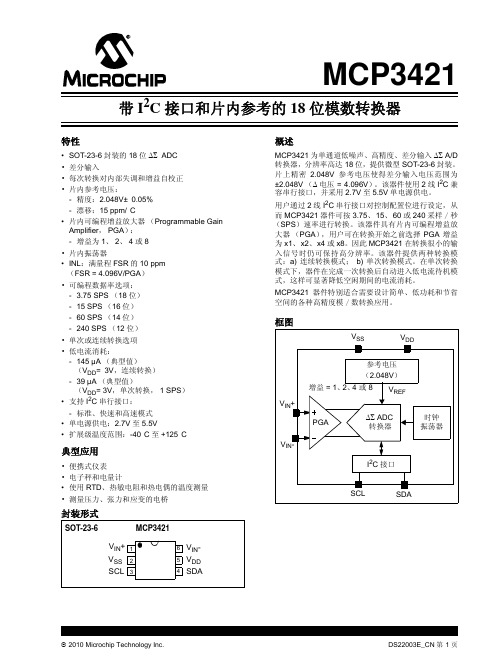
框图
VSS VDD
参考电压 (2.048V) 增益 = 1、 2、 4或8 VIN+ PGA VINI2C 接口 ADC 转换器 时钟 振荡器 VREF
典型应用
• 便携式仪表 • 电子秤和电量计 • 使用 RTD、热敏电阻和热电偶的温度测量 • 测量压力、张力和应变的电桥
SCL
SDA
封装形式
SOT-23-6 MCP3421
FSR 的 DR = 3.75 SPS (注 6) ppm
VREF — 2.048 — V 内部参考电压 注 1: 低于或超过此电压值的任意输入电压将导致泄漏电流流过输入引脚 ESD 二极管。 此参数为特征参数,未经 100% 测试。 2: 输入阻抗是由内部 3.2 pF 的输入采样电容产生的。 3: 4: 5: 6: 7: 8: 总转换速度包括自动失调和增益校正过程。 INL 是端点线与量化带宽中点测量码之差。 包括由片内 PGA 和 VREF 引起的所有误差。 满量程 (FSR) = 2 x 2.048/PGA = 4.096/PGA。 该参数为特征参数,未经 100% 测试。 该参数由设计确保,未经 100% 测试。
VOS
— — — — — —
VDD IDDA IDDS VIH VIL VOL VHYST IDDB IILH IILL
2.7 — — — 0.7 VDD — — 0.05VDD — — -1 —
— 155 145 0.1 — — — — — — — —
5.5 190 — 0.5 VDD 0.3VDD 0.4 — 10 1 — 10
VIN+ VSS SCL
1 2 3
6 5 4
VINVDD SDA
2010 Microchip Technology Inc.
MAX4211EEUE中文资料
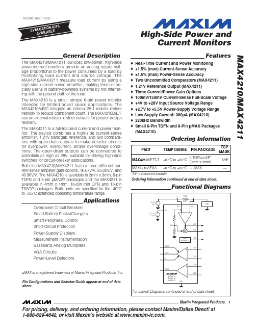
4V TO 28V
+ -
+ -
25:1
IOUT POUT
1.21V REFERENCE INHIBIT
REF
CIN1+
COUT1 CIN1LE CIN2+ COUT2
µMAX is a registered trademark of Maxim Integrated Products, Inc. Pin Configurations and Selector Guide appear at end of data sheet.
MAX4211A MAX4211B MAX4211C GND
CIN2-
Functional Diagrams continued at end of data sheet. ________________________________________________________________ Maxim Integrated Products 1
For pricing, delivery, and ordering information, please contact Maxim/Dallas Direct! at 1-888-629-4642, or visit Maxim’s website at .
元器件交易网
MAX4210/MAX4211
The MAX4210/MAX4211 low-cost, low-power, high-side power/current monitors provide an analog output voltage proportional to the power consumed by a load by multiplying load current and source voltage. The MAX4210/MAX4211 measure load current by using a high-side current-sense amplifier, making them especially useful in battery-powered systems by not interfering with the ground path of the load. The MAX4210 is a small, simple 6-pin power monitor intended for limited board space applications. The MAX4210A/B/C integrate an internal 25:1 resistor-divider network to reduce component count. The MAX4210D/E/F use an external resistor-divider network for greater design flexibility. The MAX4211 is a full-featured current and power monitor. The device combines a high-side current-sense amplifier, 1.21V bandgap reference, and two comparators with open-drain outputs to make detector circuits for overpower, overcurrent, and/or overvoltage conditions. The open-drain outputs can be connected to potentials as high as 28V, suitable for driving high-side switches for circuit-breaker applications. Both the MAX4210/MAX4211 feature three different current-sense amplifier gain options: 16.67V/V, 25.00V/V, and 40.96V/V. The MAX4210 is available in 3mm x 3mm, 6-pin TDFN and 8-pin µMAX® packages and the MAX4211 is available in 4mm x 4mm, 16-pin thin QFN and 16-pin TSSOP packages. Both parts are specified for the -40°C to +85°C extended operating temperature range.
MAX3221CAE中文资料
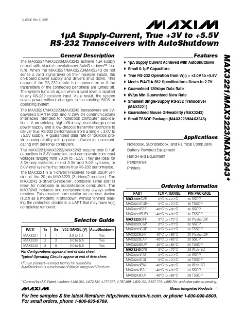
* Covered by U.S. Patent numbers 4,636,930; 4,679,134; 4,777,577; 4,797,899; 4,809,152; 4,897,774; 4,999,761; and other patents pending. ________________________________________________________________ Maxim Integrated Products 1
____________________________Features
o 1µA Supply Current Achieved with AutoShutdown o Small 0.1µF Capacitors o True RS-232 Operation from VCC = +3.0V to +5.5V o Meets EIA/TIA-562 Specifications Down to 2.7V o Guaranteed 120kbps Data Rate o 6V/µs Min Guaranteed Slew Rate o Smallest Single-Supply RS-232 Transceiver (MAX3221) o Guaranteed Mouse Driveability (MAX3243) o Small TSSOP Package (MAX31/MAX3223/MAX3243*
________________________Applications
Notebook, Subnotebook, and Palmtop Computers Battery-Powered Equipment Hand-Held Equipment Peripherals Printers
inspiron 14 3421手册
Inspiron 14/14R用户手册计算机型号:Inspiron 3421/5421管制型号:P37G管制类型:P37G001注、小心和警告注:“注”表示可以帮助您更好地使用计算机的重要信息。
小心:“小心”表示如果不遵循说明,就有可能损坏硬件或导致数据丢失。
警告:“警告”表示可能会导致财产损失、人身伤害甚至死亡。
____________________© 2012 Dell Inc.本文件中使用的商标:Dell™、DELL 徽标和 Inspiron™是 Dell Inc. 的商标;Microsoft®、Windows®和 Windows 开始按钮徽标是 Microsoft Corporation 在美国和/或其他国家或地区的商 标或注册商标;Bluetooth®是 Bluetooth SIG, Inc. 拥有的注册商标,Dell 在其许可下使用。
2012 - 11 Rev. A00目录开始操作之前 (9)关闭计算机及所连接设备的电源 (9)安全说明 (10)建议工具 (10)拆装计算机内部组件之后 (11)取出电池 (12)步骤 (12)更换电池 (13)步骤 (13)卸下光盘驱动器 (14)前期操作 (14)步骤 (14)装回光盘驱动器 (16)步骤 (16)后续条件 (16)卸下键盘 (17)前期操作 (17)步骤 (17)装回键盘 (20)步骤 (20)后续条件 (20)卸下基座盖 (21)前期操作 (21)步骤 (21)装回基座盖 (22)步骤 (22)后续条件 (22)目录 | 3卸下内存模块 (23)前期操作 (23)步骤 (23)装回内存模块 (24)步骤 (24)后续条件 (24)卸下硬盘驱动器 (25)前期操作 (25)步骤 (25)装回硬盘驱动器 (27)步骤 (27)后续条件 (27)卸下无线小型插卡 (28)前期操作 (28)步骤 (28)装回无线小型插卡 (30)步骤 (30)后续条件 (30)卸下掌垫 (31)前期操作 (31)步骤 (31)装回掌垫 (35)步骤 (35)后续条件 (35)卸下币形电池 (36)前期操作 (36)步骤 (37)4 | 目录装回币形电池 (38)步骤 (38)后续条件 (38)卸下 I/O 板 (39)前期操作 (39)步骤 (40)装回 I/O 板 (41)步骤 (41)后续条件 (41)卸下电源适配器端口 (42)前期操作 (42)步骤 (43)装回电源适配器端口 (45)步骤 (45)后续条件 (45)卸下系统板 (46)前期操作 (46)步骤 (47)更换系统板 (49)步骤 (49)后续条件 (49)在系统设置中输入服务标签 (49)卸下热冷却部件 (50)前期操作 (50)步骤 (50)装回热冷却部件 (51)步骤 (51)后续条件 (51)卸下扬声器 (52)前期操作 (52)步骤 (53)目录 | 5装回扬声器 (54)步骤 (54)后续条件 (54)卸下显示屏部件 (55)前期操作 (55)步骤 (56)装回显示屏部件 (57)步骤 (57)后续条件 (57)卸下显示屏挡板 (58)前期操作 (58)步骤 (59)装回显示屏挡板 (60)步骤 (60)后续条件 (60)卸下显示屏铰链部件 (61)前期操作 (61)步骤 (62)装回显示屏铰链部件 (63)步骤 (63)后续条件 (63)卸下显示屏面板 (64)前期操作 (64)步骤 (65)装回显示屏面板 (66)步骤 (66)后续条件 (66)卸下摄像头模块 (67)前期操作 (67)步骤 (68)6 | 目录装回摄像头模块 (69)步骤 (69)后续条件 (69)刷新 BIOS (70)目录 | 78 | 目录开始操作之前 | 9开始操作之前关闭计算机及所连接设备的电源小心:为避免数据丢失,请在关机之前,保存并关闭所有打开的文件,并退出所有打开的程序。
Magellan_eXplorist_110_用户手册

第 2 页 共 47 页
Magellan eXplorist 110 用户手册
重要注意事项:
FCC辐射暴露声明:
本设备符合 FCC 针对未受控制环境所制定的辐射暴露限制。最终用户必须遵守射频暴露符合性的特定使用说明。 本发射设备不能与设在同一地点的任何其他天线或发射器一起工作。 为符合FCC规则,必须屏蔽本设备电缆。使用非准许设备或者非屏蔽电缆易导致无线电和TV接收机干扰。用户应注 意未经制造商许可的变化和修改可能导致有损用户使用该设备的权利。
使用合适的配件.................................................................................................................................................................................. 2
重要注意事项:.................................................................................................................................................................................. 3
重要注意事项:
IC辐射暴露声明:
本设备符合针对未受控制环境所制定的IC辐射暴露限制。最终用户必须遵守满足射频暴露符合性的特定使用说明 书。 本发射机不能与任何其他天线或发射机在同一地点或连接。 本文档所包含的信息可随时更改,不另行通知。 本产品改良,不另行通知,请点击麦哲伦网站()进行产品升级,获取附加说明。 正常最高使用温度为66℃。 © 2011神达电脑(MiTAC International Corporation)版权所有。 Magellan、Magellan标志和eXplorist为神达电脑之商 标,已在美国或/及其它国家注册,并授权MiTAC Digital Corp. 使用。保留所有权利。
MAX490EEPA中文资料
元器件交易网
MAX481E/MAX483E/MAX485E/MAX487E–MAX491E/MAX1487E
19-0410; Rev 4; 10/03
±15kV ESD-Protected, Slew-Rate-Limited, Low-Power, RS-485/RS-422 Transceivers
Ordering Information
PART MAX481ECPA MAX481ECSA MAX481EEPA MAX481EESA MAX483ECPA MAX483ECSA MAX483EEPA MAX483EESA
TEMP RANGE 0°C to +70°C 0°C to +70°C -40°C to +85°C -40°C to +85°C 0°C to +70°C 0°C to +70°C -40°C to +85°C -40°C to +85°C
usb接口芯片

第7章USB接口芯片7.1 USB接口芯片分类USB专用的器件大致可以分为以下类型:•USB主控制器•USB根集线器,•微处理器接口的USB专用接口芯片•具有USB接口的微处理器•USB桥芯片•OTG专用芯片其中前两类用于计算机,一般集成于计算机的芯片组中。
在实际的开发中大多项目是针对USB外部设备,用于USB设备的芯片主要是USB专用接口芯片和具有USB接口的微处理器。
USB专用接口芯片内部不包含通用微处理器,提供与通用微处理器的接口电路,可以与大多数微处理器连接,固件的编程在微处理器完成,主要用于基于微处理器的计算机外部设备开发。
USB桥芯片,可以将USB接口转换成为串行接口、并行接口、IrDA等其他标准接口,这类芯片不需要固件编程。
7.2 微处理器接口的USB专用接口器件具备微处理器接口的USB接口芯片与微处理器的接口是不统一的,根据芯片的设计的不同,可以通过通用的串行接口、并行接口、SPI等接口和微处理器连接。
USB接口芯片主要由以下部分组成:•USB收发器•SIE(Serial Interface Engine)•数据缓冲存储器FIFO•时钟及控制逻辑•微处理器接口逻辑这类芯片常用的有Philips公司的PDIUSBD11和PDIUSBD12;National Semiconductor公司的USBN9602、9603和9604;MAXIM公司的MAX3420、MAX3421等。
下表是几种常见的USB专用接口芯片的基本情况。
162 计算机高级接口实践下面对这几款芯片的硬件作简要介绍。
7.2.1 Philips 的PDIUSBD12Philips 的D12是使用很广泛的USB 控制器,主要的特点包括:• 支持控制、中断、批量和实时四种传输模式,批量和实时模式可以达到1MB/sec的传输速率;• 集成了总共320字节的FIFO ,并且在不同的模式下可以灵活分配。
对于中断和批量模式支持2X64字节的双缓冲,对于实时模式支持2X128字节的双缓冲; • 支持完全自动的DMA 接口;• 并行方式的微处理器接口,可以达到最大2MB/sec 的传输速率。
笔记本电源管理芯片

笔记本电源管理芯片,i/o(2009-11-06 22:23:06)转载标签:杂谈笔记本电源管理芯片大全:ADP3421/ADP3410/ADP3205/ADP3180/ADP3806/ADP3203/ADP3020电源管理芯片大全RT9237/RT9237CS/RT9231/RT9241/RT9231A/RT9241A/RT9241B电源管理芯片大全RT9221/RT9600/RT9602/RT9603/RT9222/RT9224/RT9224A/RT9223电源管理芯片大全RT9227A/RT9228/RT9238/RT9248A/RT9173/RT9202/RC5051M 电源管理芯片大全5090MTC/RC5093MTC/5098MTC/SC1470/SC1205/SC1214TS电源管理芯片大全SC1155CSW/SC1154CSW/SC1153CSW/SC1189SW//SC1185ACSW电源管理芯片大全SC1402ISS/SC2422ACS//SC1164CSW/SC1150/ISL6524CB/RC5053M电源管理芯片大全/ISL6522CB/ISL6556BCB/ISL6566CRZ/4500M/HIP6501ACB电源管理芯片大全HIP6521CB/HIP6502/HIP6016CB/HIP6017CB/HIP6018BCB/HIP6019BCB电源管理芯片大全HIP6020CB/HIP6021CB/HIP6601/HIP6602BCB/HIP6603CB/HIP6004ECB电源管理芯片大全HIP6620BAB/HIP6301CB/HIP6520/HIP6302CB/HIP6303CS/SC1163电源管理芯片大全SC1159/SC1486/ST75185C/SC2434SW/SC1480/SC1403/SC1404 电源管理芯片大全SC1485/SC1486/SC1474/SC1476/SC1211/SC451/SC1470电源管理芯片大全IRU3013/IRU3004CW/IRU3055CQTR/IRU1150CM/MS-5/MS-7/5322电源管理芯片大全CS5301/L6916D/L6917CB/LM2637M/LM2638M/ICE2AS01/KA7500B笔记本电源管理芯片ADP3421/ADP3410/ADP3205/ADP3180/ADP3806/ADP3203/ADP3020笔记本电源管理芯片ADP3170/ADP3188/ADP3181/ADP3166/ADP3163/ADP3165/ADP3168笔记本电源管理芯片ADP3169/ADP3415/ADP3416/ADP3417/ADP3418/ADP3155/ADP3422笔记本电源管理芯片ADP3207/MAX3243/MAX1902/MAX1999/MAX785/MAX786/MAX1717笔记本电源管理芯片MAX1604/MAX1987/MAX1887/ISL6223/ISL6565/ISL6225/ISL6218笔记本电源管理芯片ISL6566/ISL6568/ISL6563笔记本电源管理芯片MAX1904(SSOP)/MAX1904(BGA的)/MAX1634/MAX1710/MAX1711笔记本电源管理芯片MAX1904/MAX1714/MAX1715/MAX1718/MAX1772/MAX1773/MAX1901笔记本电源管理芯片MAX1908/MAX1632/MAX1545/MAX1535/MAX1631/MAX1909/MAX1977笔记本电源管理芯片MAX1504/MAX1845/MAX1844/MAX1980/MAX1532/MAX1907/MAX1617笔记本电源管理芯片MAX8734/MAX8743/MAX8724/MAX1644/MAX1645/ISL6207/ISL6559CB笔记本电源管理芯片ISL6217/ISL6264/ISL6227/ISL6255/SC1485/SC1404笔记本电源管理芯片LT3728LX/LTC1709/LTC1439/LTC3735/LTC1628/LTC1707/LTC1736笔记本电源管理芯片MB3887/MB3878/LTC1778/LTC1511/LTC1709/LTC1439/LM8463笔记本电源管理芯片LM2729/LM2641/VT8235/LTC3728/SC1476/SC1474/SC1404/SC451笔记本电源管理芯片SC1403/SC1470/SC1486/TPS51120/TPS51020/PU2211A/VT6105笔记本电源管理芯片VT8235/VT1612/VT8237/VT8233/VT8235(BGA的)/LTC3707/LTC3716笔记本IO芯片大全PC87591S(VPCQ01)/PC 87591L(VPC01)/PC 97317IBW/PC 87393 VGJ笔记本IO芯片大全TB62501F/TB62506F/TB6808F/KB910QF/KB910QB4/KB910LQF/KB910LQFA1笔记本IO芯片大全KB3910QB0/KB910SFC1/KB3910SF/PC87591E-VLB/IT8510E/PS5130笔记本IO芯片大全PC87591E (-VPCI01),(VPCQ01)/PC 97551-VPC/PC87570-ICC/VPC笔记本IO芯片大全PC87391VGJ/TB6807F/W83L950D/LPC47N249-AQQ/PCI4510/PC8394T笔记本IO芯片大全PC87392/PC87541L/PC87541V/LPC47N253-AQQ/PC87591E-VLB笔记本IO芯片大全LPC47N250-SD/LPC47N252-SG/LPC47N254-AQQ。
MCP3421A3T-ECH;MCP3421A2T-ECH;MCP3421A0T-ECH;MCP3421A1T-ECH;中文规格书,Datasheet资料
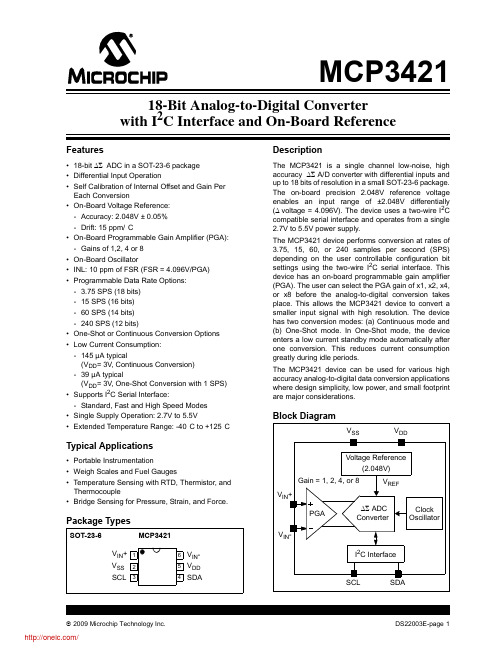
Block Diagram
VSS
VDD
Voltage Reference
(2.048V)
Gain = 1, 2, 4, or 8
VREF
VIN+
PGA
ΔΣ ADC Converter
Clock Oscillator
VIN-
I2C Interface
SCL
SDA
© 2009 Microchip Technology Inc.
V
Differential Input Impedance
ZIND (f)
—
2.25/PGA
—
(Note 2)
MΩ During normal mode operation
Common Mode input Impedance
ZINC (f)
—
25
—
MΩ PGA = 1, 2, 4, 8
System Performance
SPS S1,S0 = ‘00’, (12 bits mode)
44
60
82
SPS S1,S0 = ‘01’, (14 bits mode)
11
15
20.5
SPS S1,S0 = ‘10’, (16 bits mode)
2.75
3.75
5.1
SPS S1,S0 = ‘11’, (18 bits mode)
VREF
—
2.048
—
V
Note 1: Any input voltage below or greater than this voltage causes leakage current through the ESD diodes at the input pins.
MAX3081E中文资料
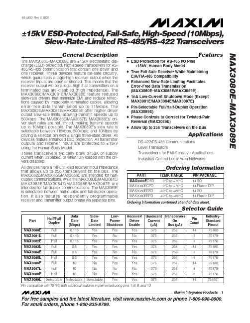
Ordering Information
PART MAX3080ECSD MAX3080ECPD MAX3080EESD MAX3080EEPD
TEMP. RANGE 0°C to +70°C 0°C to +70°C
-40°C to +85°C -40°C to +85°C
PIN-PACKAGE 14 SO 14 Plastic DIP 14 SO 14 Plastic DIP
o Allow Up to 256 Transceivers on the Bus
Applications
RS-422/RS-485 Communications Level Translators Transceivers for EMI-Sensitive Applications Industrial-Control Local Area Networks
Ordering Information continued at end of data sheet.
Selector Guide
Part
Half/Full Duplex
Data Rate (Mbps)
SlewRate Limited
Low- Receiver/ Quiescent Transceivers
MAX3241ECAI中文资料
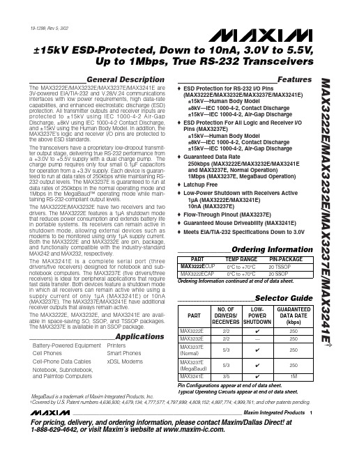
General DescriptionThe MAX3222E/MAX3232E/MAX3237E/MAX3241E are 3V-powered EIA/TIA-232 and V.28/V.24 communications interfaces with low power requirements, high data-rate capabilities, and enhanced electrostatic discharge (ESD)protection. All transmitter outputs and receiver inputs are protected to ±15kV using IEC 1000-4-2 Air-G ap Discharge, ±8kV using IEC 1000-4-2 Contact Discharge,and ±15kV using the Human Body Model. In addition, the MAX3237E’s logic and receiver I/O pins are protected to the above ESD standards.The transceivers have a proprietary low-dropout transmit-ter output stage, delivering true RS-232 performance from a +3.0V to +5.5V supply with a dual charge pump. The charge pump requires only four small 0.1µF capacitors for operation from a +3.3V supply. Each device is guaran-teed to run at data rates of 250kbps while maintaining RS-232 output levels. The MAX3237E is guaranteed to run at data rates of 250kbps in the normal operating mode and 1Mbps in the MegaBaud™ operating mode while main-taining RS-232-compliant output levels.The MAX3222E/MAX3232E have two receivers and two drivers. The MAX3222E features a 1µA shutdown mode that reduces power consumption and extends battery life in portable systems. Its receivers can remain active in shutdown mode, allowing external devices such as modems to be monitored using only 1µA supply current.Both the MAX3222E and MAX3232E are pin, package,and functionally compatible with the industry-standard MAX242 and MAX232, respectively.The MAX3241E is a complete serial port (three drivers/five receivers) designed for notebook and sub-notebook computers. The MAX3237E (five drivers/three receivers) is ideal for peripheral applications that require fast data transfer. Both devices feature a shutdown mode in which all receivers can remain active while using a supply current of only 1µA (MAX3241E) or 10nA (MAX3237E). The MAX3237E/MAX3241E have additional receiver outputs that always remain active.The MAX3222E, MAX3232E, and MAX3241E are avail-able in space-saving SO, SSOP, and TSSOP packages.The MAX3237E is available in an SSOP package.________________________ApplicationsBattery-Powered Equipment PrintersCell PhonesSmart Phones Cell-Phone Data Cables xDSL ModemsNotebook, Subnotebook, and Palmtop ComputersFeatureso ESD Protection for RS-232 I/O Pins(MAX3222E/MAX3232E/MAX3237E/MAX3241E)±15kV—Human Body Model±8kV—IEC 1000-4-2, Contact Discharge ±15kV—IEC 1000-4-2, Air-Gap Discharge o ESD Protection For All Logic and Receiver I/O Pins (MAX3237E)±15kV—Human Body Model±8kV—IEC 1000-4-2, Contact Discharge ±15kV—IEC 1000-4-2, Air-Gap Discharge o Guaranteed Data Rate250kbps (MAX3222E/MAX3232E/MAX3241E and MAX3237E, Normal Operation)1Mbps (MAX3237E, MegaBaud Operation)o Latchup Freeo Low-Power Shutdown with Receivers Active1µA (MAX3222E/MAX3241E)10nA (MAX3237E)o Flow-Through Pinout (MAX3237E)o Guaranteed Mouse Driveability (MAX3241E)o Meets EIA/TIA-232 Specifications Down to 3.0VMAX3222E/MAX3232E/MAX3237E/MAX3241E †±15kV ESD-Protected, Down to 10nA, 3.0V to 5.5V ,Up to 1Mbps, True RS-232 Transceivers________________________________________________________________Maxim Integrated Products119-1298; Rev 5; 3/02MegaBaud is a trademark of Maxim Integrated Products, Inc.†Covered by U.S. Patent numbers 4,636,930; 4,679,134; 4,777,577; 4,797,899; 4,809,152; 4,897,774; 4,999,761; and other patents pending.For pricing, delivery, and ordering information,please contact Maxim/Dallas Direct!at 1-888-629-4642, or visit Maxim’s website at .M A X 3222E /M A X 3232E /M A X 3237E /M A X 3241E±15kV ESD-Protected, Down to 10nA, 3.0V to 5.5V ,Up to 1Mbps, True RS-232 TransceiversABSOLUTE MAXIMUM RATINGSELECTRICAL CHARACTERISTICSStresses beyond those listed under “Absolute Maximum Ratings” may cause permanent damage to the device. These are stress ratings only, and functional operation of the device at these or any other conditions beyond those indicated in the operational sections of the specifications is not implied. Exposure to absolute maximum rating conditions for extended periods may affect device reliability.V CC to GND..............................................................-0.3V to +6V V+ to GND (Note 1)..................................................-0.3V to +7V V- to GND (Note 1)...................................................+0.3V to -7V V+ + |V-| (Note 1).................................................................+13V Input VoltagesT_IN, EN , SHDN , MBAUD to GND ........................-0.3V to +6V R_IN to GND.....................................................................±25V Output VoltagesT_OUT to GND...............................................................±13.2V R_OUT, R_OUTB (MAX3241E)................-0.3V to (V CC + 0.3V)Short-Circuit Duration, T_OUT to GND.......................Continuous Continuous Power Dissipation (T A = +70°C)16-Pin SSOP (derate 7.14mW/°C above +70°C)..........571mW 16-Pin Wide SO (derate 9.52mW/°C above +70°C).....762mW18-Pin Wide SO (derate 9.52mW/°C above +70°C).....762mW 18-Pin PDIP (derate 11.11mW/°C above +70°C)..........889mW 20-Pin TSSOP (derate 10.9mW/°C above +70°C)........879mW 20-Pin SSOP (derate 8.00mW/°C above +70°C)..........640mW 28-Pin SSOP (derate 9.52mW/°C above +70°C)..........762mW 28-Pin Wide SO (derate 12.50mW/°C above +70°C).............1W 28-Pin TSSOP (derate 12.8mW/°C above +70°C)......1026mW 32-pin QFN (derate 23.2mW/°C above +70°C).............1860mW Operating Temperature RangesMAX32_ _EC_ _...................................................0°C to +70°C MAX32_ _EE_ _.................................................-40°C to +85°C Storage Temperature Range.............................-65°C to +150°C Lead Temperature (soldering, 10s).................................+300°CNote 1:V+ and V- can have maximum magnitudes of 7V, but their absolute difference cannot exceed 13V.MAX3222E/MAX3232E/MAX3237E/MAX3241E±15kV ESD-Protected, Down to 10nA, 3.0V to 5.5V ,Up to 1Mbps, True RS-232 TransceiversELECTRICAL CHARACTERISTICS (continued)(V CC = +3.0V to +5.5V, C1–C4 = 0.1µF, T A = T MIN to T MAX , unless otherwise noted. Typical values are at T A = +25°C.) (Note 2)(V CC = +3.0V to +5.5V, C1–C4 = 0.1µF, T A = T MIN to T MAX , unless otherwise noted. Typical values are at T A = +25°C.) (Note 2)__________________________________________Typical Operating Characteristics(V CC = +3.3V, 250kbps data rate, 0.1µF capacitors, all transmitters loaded with 3k Ωand C L , T A = +25°C, unless otherwise noted.)-6-5-4-3-2-10123456010002000300040005000MAX3222E/MAX3232ETRANSMITTER OUTPUT VOLTAGEvs. LOAD CAPACITANCELOAD CAPACITANCE (pF)T R A N S M I T T E R O U T P U T V O L T A G E (V )624108141216010002000300040005000MAX3222E/MAX3232ESLEW RATE vs. LOAD CAPACITANCELOAD CAPACITANCE (pF)S L E W R A T E (V /µs )2520155103530404520001000300040005000MAX3222E/MAX3232E OPERATING SUPPLY CURRENT vs. LOAD CAPACITANCELOAD CAPACITANCE (pF)S U P P L Y C U R R E N T (m A )M A X 3222E /M A X 3232E /M A X 3237E /M A X 3241E±15kV ESD-Protected, Down to 10nA, 3.0V to 5.5V ,Up to 1Mbps, True RS-232 Transceivers4_______________________________________________________________________________________TIMING CHARACTERISTICS —MAX3237ENote 2:MAX3222E/MAX3232E/MAX3241E: C1–C4 = 0.1µF tested at 3.3V ±10%; C1 = 0.047µF, C2, C3, C4 = 0.33µF tested at 5.0V±10%. MAX3237E: C1–C4 = 0.1µF tested at 3.3V ±5%, C1–C4 = 0.22µF tested at 3.3V ±10%; C1 = 0.047µF, C2, C3, C4 =0.33µF tested at 5.0V ±10%.Note 3:The MAX3237E logic inputs have an active positive feedback resistor. The input current goes to zero when the inputs are atthe supply rails.Note 4:Transmitter skew is measured at the transmitter zero crosspoints.MAX3222E/MAX3232E/MAX3237E/MAX3241E±15kV ESD-Protected, Down to 10nA, 3.0V to 5.5V ,Up to 1Mbps, True RS-232 Transceivers_______________________________________________________________________________________5-6-2-42046-5-31-135010001500500200025003000LOAD CAPACITANCE (pF)T R A N S M I T T E R O U T P U T V O L T A G E (V )MAX3237ETRANSMITTER OUTPUT VOLTAGEvs. LOAD CAPACITANCE010203050406070MAX3237ESLEW RATE vs. LOAD CAPACITANCE(MBAUD = V CC )LOAD CAPACITANCE (pF)S L E W R A T E (V /µs )500100015002000-7.5-5.0-2.502.55.07.5MAX3237ETRANSMITTER OUTPUT VOLTAGE vs. LOAD CAPACITANCE (MBAUD = V CC )LOAD CAPACITANCE (pF)T R A N S M I T T E R O U T P U T V O L T A G E (V )50010001500200024681012MAX3237ESLEW RATE vs. LOAD CAPACITANCE(MBAUD = GND)LOAD CAPACITANCE (pF)S L E W R A T E (V /µs )100015005002000250030001020304050MAX3237ESUPPLY CURRENT vs. LOAD CAPACITANCE WHEN TRANSMITTING DATA (MBAUD = GND)LOAD CAPACITANCE (pF)S U P P L Y C U R R E N T (m A )1000150050020002500300020604080100MAX3237ETRANSMITTER SKEW vs. LOAD CAPACITANCE(MBAUD = V CC )LOAD CAPACITANCE (pF)100015005002000T R A N S M I T T E R S K E W (n s )Typical Operating Characteristics (continued)(V CC = +3.3V, 250kbps data rate, 0.1µF capacitors, all transmitters loaded with 3k Ωand C L, T A = +25°C, unless otherwise noted.)-6-5-4-3-2-10123456010002000300040005000MAX3241ETRANSMITTER OUTPUT VOLTAGEvs. LOAD CAPACITANCELOAD CAPACITANCE (pF)T R A N S M I T T E R O U T P U T V O L T A G E (V )302010405060020001000300040005000MAX3241EOPERATING SUPPLY CURRENT vs. LOAD CAPACITANCELOAD CAPACITANCE (pF)S U P P L Y C U R R E N T (m A )04286121014010002000300040005000MAX3241ESLEW RATE vs. LOAD CAPACITANCEM A X 3237E t o c 05LOAD CAPACITANCE (pF)S L E W R A T E (V /µs )Pin DescriptionM A X 3222E /M A X 3232E /M A X 3237E /M A X 3241E±15kV ESD-Protected, Down to 10nA, 3.0V to 5.5V ,Up to 1Mbps, True RS-232 TransceiversTypical Operating Characteristics (continued)(V CC = +3.3V, 250kbps data rate, 0.1µF capacitors, all transmitters loaded with 3k Ωand C L , T A = +25°C, unless otherwise noted.)-6-2-42046-3-51-1352.03.0 3.52.54.0 4.55.0SUPPLY VOLTAGE (V)T R A N S M I T T E R O U T P U T V O L T A G E (V )MAX3237ETRANSMITTER OUTPUT VOLTAGE vs.SUPPLY VOLTAGE (MBAUD = GND)10203040502.0MAX3237ESUPPLY CURRENT vs.SUPPLY VOLTAGE (MBAUD = GND)SUPPLY VOLTAGE (V)S U P P L Y C U R R E N T (m A )3.03.52.54.04.55.0MAX3222E/MAX3232E/MAX3237E/MAX3241E±15kV ESD-Protected, Down to 10nA, 3.0V to 5.5V ,Up to 1Mbps, True RS-232 Transceivers_______________________________________________________________________________________7Figure 1. Slew-Rate Test CircuitsM A X 3222E /M A X 3232E /M A X 3237E /M A X 3241E±15kV ESD-Protected, Down to 10nA, 3.0V to 5.5V ,Up to 1Mbps, True RS-232 Transceivers_______________Detailed DescriptionDual Charge-Pump Voltage ConverterThe MAX3222E/MAX3232E/MAX3237E/MAX3241E ’s internal power supply consists of a regulated dual charge pump that provides output voltages of +5.5V (doubling charge pump) and -5.5V (inverting charge pump), over the 3.0V to 5.5V V CC range. The charge pump operates in discontinuous mode; if the output voltages are less than 5.5V, the charge pump is enabled, and if the output voltages exceed 5.5V, the charge pump is disabled. Each charge pump requires a flying capacitor (C1, C2) and a reservoir capacitor (C3, C4) to generate the V+ and V- supplies (Figure 1).RS-232 TransmittersThe transmitters are inverting level translators that con-vert TTL/CMOS-logic levels to ±5.0V EIA/TIA-232 com-pliant levels.The MAX3222E/MAX3232E/MAX3237E/MAX3241E transmitters guarantee a 250kbps data rate with worst-case loads of 3k Ωin parallel with 1000pF, providing compatibility with PC-to-PC communication software (such as LapLink ™). Transmitters can be paralleled to drive multiple receivers or mice.The MAX3222E/MAX3237E/MAX3241E ’s transmitters are disabled and the outputs are forced into a high-imped-ance state when the device is in shutdown mode (SHDN =GND). The MAX3222E/MAX3232E/MAX3237E/MAX3241E permit the outputs to be driven up to ±12V in shutdown.The MAX3222E/MAX3232E/MAX3241E transmitter inputs do not have pullup resistors. Connect unused inputs to G ND or V CC . The MAX3237E ’s transmitter inputs have a 400k Ωactive positive feedback resistor,allowing unused inputs to be left unconnected.MAX3237E MegaBaud OperationFor higher-speed serial communications, the MAX3237E features MegaBaud operation. In MegaBaud operating mode (MBAUD = V CC ), the MAX3237E transmitters guarantee a 1Mbps data rate with worst-case loads of 3k Ωin parallel with 250pF for 3.0V < V CC < 4.5V. For 5V ±10% operation, the MAX3237E transmitters guarantee a 1Mbps data rate into worst-case loads of 3k Ωin parallel with 1000pF.RS-232 ReceiversThe receivers convert RS-232 signals to CMOS-logic output levels. The MAX3222E/MAX3237E/MAX3241E receivers have inverting three-state outputs. Drive EN high to place the receiver(s) into a high-impedancestate. Receivers can be either active or inactive in shut-down (Table 1).The complementary outputs on the MAX3237E/MAX3241E (R_OUTB) are always active, regardless of the state of EN or SHDN . This allows the device to be used for ring indica-tor applications without forward biasing other devices con-nected to the receiver outputs. This is ideal for systems where V CC drops to 0 in shutdown to accommodate peripherals such as UARTs (Figure 2).MAX3222E/MAX3237E/MAX3241EShutdown ModeSupply current falls to less than 1µA in shutdown mode (SHDN = low). The MAX3237E ’s supply current falls to10nA (typ) when all receiver inputs are in the invalid range (-0.3V < R_IN < +0.3). When shut down, the device ’s charge pumps are shut off, V+ is pulled down to V CC , V- is pulled to ground, and the transmitter outputs are disabled (high impedance). The time required to recover from shutdown is typically 100µs,as shown in Figure 3. Connect SHDN to V CC if the shut-down mode is not used. SHDN has no effect on R_OUT or R_OUTB (MAX3237E/MAX3241E).±15kV ESD ProtectionAs with all Maxim devices, ESD-protection structures are incorporated to protect against electrostatic dis-charges encountered during handling and assembly.The driver outputs and receiver inputs of the MAX3222E/MAX3232E/MAX3237E/MAX3241E have extra protection against static electricity. Maxim ’s engi-neers have developed state-of-the-art structures to pro-tect these pins against ESD of ±15kV without damage.The ESD structures withstand high ESD in all states:normal operation, shutdown, and powered down. After an ESD event, Maxim ’s E versions keep working without latchup, whereas competing RS-232 products can latch and must be powered down to remove latchup.Furthermore, the MAX3237E logic I/O pins also have ±15kV ESD protection. Protecting the logic I/O pins to ±15kV makes the MAX3237E ideal for data cable appli-cations.LapLink is a trademark of Traveling Software.8MAX3222E/MAX3232E/MAX3237E/MAX3241E±15kV ESD-Protected, Down to 10nA, 3.0V to 5.5V ,Up to 1Mbps, True RS-232 Transceivers_______________________________________________________________________________________9ESD protection can be tested in various ways; the transmitter outputs and receiver inputs for the MAX3222E/MAX3232E/MAX3237E/MAX3241E are characterized for protection to the following limits:•±15kV using the Human Body Model•±8kV using the Contact Discharge method specified in IEC 1000-4-2•±15kV using IEC 1000-4-2’s Air-G ap Discharge method ESD Test ConditionsESD performance depends on a variety of conditions.Contact Maxim for a reliability report that documents test setup, test methodology, and test results.Human Body ModelFigure 4a shows the Human Body Model, and Figure 4b shows the current waveform it generates when dis-charged into a low impedance. This model consists of a 100pF capacitor charged to the ESD voltage of inter-est, which is then discharged into the test device through a 1.5k Ωresistor.IEC 1000-4-2The IEC 1000-4-2 standard covers ESD testing and per-formance of finished equipment; it does not specifically refer to integrated circuits. The MAX3222E/MAX3232E/MAX3237E/MAX3241E help you design equipment that meets Level 4 (the highest level) of IEC 1000-4-2, without the need for additional ESD-protection components.The major difference between tests done using the Human Body Model and IEC 1000-4-2 is higher peak current in IEC 1000-4-2 because series resistance is lower in the IEC 1000-4-2 model. Hence, the ESD with-stand voltage measured to IEC 1000-4-2 is generally lower than that measured using the Human Body Model. Figure 5a shows the IEC 1000-4-2 model, and Figure 5b shows the current waveform for the ±8kV IEC 1000-4-2 Level 4 ESD Contact Discharge test.The Air-G ap Discharge test involves approaching the device with a charged probe. The Contact DischargeFigure 2. Detection of RS-232 Activity when the UART andInterface are Shut Down; Comparison of MAX3237E/MAX3241E (b) with Previous Transceivers (a)40µs/divV CC = 3.3V C1–C4 = 0.1µFFigure 3. Transmitter Outputs Recovering from Shutdown or Powering UpM A X 3222E /M A X 3232E /M A X 3237E /M A X 3241E±15kV ESD-Protected, Down to 10nA, 3.0V to 5.5V ,Up to 1Mbps, True RS-232 Transceivers10______________________________________________________________________________________method connects the probe to the device before the probe is energized.Machine ModelThe Machine Model for ESD tests all pins using a 200pF storage capacitor and zero discharge resis-tance. Its objective is to emulate the stress caused by contact that occurs with handling and assembly during manufacturing. All pins require this protection during manufacturing, not just RS-232 inputs and outputs.Therefore, after PC board assembly, the Machine Model is less relevant to I/O ports.Applications InformationCapacitor SelectionThe capacitor type used for C1–C4 is not critical for proper operation; polarized or nonpolarized capacitors can be used. The charge pump requires 0.1µF capaci-tors for 3.3V operation. For other supply voltages, see Table 2for required capacitor values. Do not use val-ues smaller than those listed in Table 2. Increasing the capacitor values (e.g., by a factor of 2) reduces ripple on the transmitter outputs and slightly reduces power consumption. C2, C3, and C4 can be increased without changing C1’s value. However, do not increase C1without also increasing the values of C2, C3, C4,and C BYPASS to maintain the proper ratios (C1 to the other capacitors).Figure 4a. Human Body ESD Test Model Figure 4b. Human Body Model Current WaveformFigure 5a. IEC 1000-4-2 ESD Test Model Figure 5b. IEC 1000-4-2 ESD Generator Current WaveformMAX3222E/MAX3232E/MAX3237E/MAX3241E±15kV ESD-Protected, Down to 10nA, 3.0V to 5.5V ,Up to 1Mbps, True RS-232 Transceivers______________________________________________________________________________________11When using the minimum required capacitor values,make sure the capacitor value does not degrade excessively with temperature. If in doubt, use capaci-tors with a larger nominal value. The capacitor ’s equiv-alent series resistance (ESR), which usually rises at low temperatures, influences the amount of ripple on V+and V-.Power-Supply DecouplingIn most circumstances, a 0.1µF V CC bypass capacitor is adequate. In applications that are sensitive to power-supply noise, use a capacitor of the same value as charge-pump capacitor C1. Connect bypass capaci-tors as close to the IC as possible.Operation Down to 2.7VTransmitter outputs will meet EIA/TIA-562 levels of ±3.7V with supply voltages as low as 2.7V.Transmitter Outputs when Recovering from ShutdownFigure 3shows two transmitter outputs when recover-ing from shutdown mode. As they become active, the two transmitter outputs are shown going to opposite RS-232 levels (one transmitter input is high, the other is low). Each transmitter is loaded with 3k Ωin parallel with 2500pF. The transmitter outputs display no ringing or undesirable transients as they come out of shutdown.Note that the transmitters are enabled only when the magnitude of V- exceeds approximately -3V.Mouse DriveabilityThe MAX3241E has been specifically designed to power serial mice while operating from low-voltagepower supplies. It has been tested with leading mouse brands from manufacturers such as Microsoft and Logitech. The MAX3241E successfully drove all serial mice tested and met their respective current and volt-age requirements. Figure 6a shows the transmitter out-put voltages under increasing load current at 3.0V.Figure 6b shows a typical mouse connection using the MAX3241E.High Data RatesThe MAX3222E/MAX3232E/MAX3237E/MAX3241E maintain the RS-232 ±5.0V minimum transmitter output voltage even at high data rates. Figure 7shows a trans-mitter loopback test circuit. Figure 8shows a loopback test result at 120kbps, and Figure 9shows the same test at 250kbps. For Figure 8, all transmitters were driven simultaneously at 120kbps into RS-232 loads in parallel with 1000pF. For Figure 9, a single transmitter was driv-en at 250kbps, and all transmitters were loaded with an RS-232 receiver in parallel with 1000pF.The MAX3237 maintains the RS-232 ±5.0V minimum transmitter output voltage at data rates up to 1Mbps.Figure 10shows a loopback test result at 1Mbps with MBAUD = V CC . For Figure 10, all transmitters were loaded with an RS-232 receiver in parallel with 250pF.Interconnection with 3V and 5V LogicThe MAX3222E/MAX3232E/MAX3237E/MAX3241E can directly interface with various 5V logic families, includ-ing ACT and HCT CMOS. See Table 3for more infor-mation on possible combinations of interconnections.Figure 6a. MAX3241E Transmitter Output Voltage vs. Load Current per TransmitterM A X 3222E /M A X 3232E /M A X 3237E /M A X 3241E±15kV ESD-Protected, Down to 10nA, 3.0V to 5.5V ,Up to 1Mbps, True RS-232 Transceivers12______________________________________________________________________________________Figure 6b. Mouse Driver Test CircuitMAX3222E/MAX3232E/MAX3237E/MAX3241E±15kV ESD-Protected, Down to 10nA, 3.0V to 5.5V ,Up to 1Mbps, True RS-232 Transceivers______________________________________________________________________________________13Figure 7. Loopback Test Circuit2µs/divV CC = 3.3V C1–C4 = 0.1µFFigure 8. MAX3241E Loopback Test Result at 120kbps2µs/divV CC = 3.3V, C1–C4 = 0.1µFFigure 9. MAX3241E Loopback Test Result at 250kbpsT_INT_OUT5k ΩR_OUT400ns/divV CC = 3.3V C1–C4 = 0.1µFFigure 10. MAX3237E Loopback Test Result at 1000kbps (MBAUD = V CC )Table 3. Logic-Family Compatibility with Various Supply VoltagesM A X 3222E /M A X 3232E /M A X 3237E /M A X 3241E±15kV ESD-Protected, Down to 10nA, 3.0V to 5.5V ,Up to 1Mbps, True RS-232 Transceivers14________________________________________________________________________________________________________________________________________________Pin ConfigurationsMAX3222E/MAX3232E/MAX3237E/MAX3241E±15kV ESD-Protected, Down to 10nA, 3.0V to 5.5V ,Up to 1Mbps, True RS-232 Transceivers______________________________________________________________________________________15__________________________________________________Typical Operating CircuitsM A X 3222E /M A X 3232E /M A X 3237E /M A X 3241E±15kV ESD-Protected, Down to 10nA, 3.0V to 5.5V ,Up to 1Mbps, True RS-232 Transceivers16___________________________________________________________________________________________________________________________Typical Operating Circuits (continued)MAX3222E/MAX3232E/MAX3237E/MAX3241E±15kV ESD-Protected, Down to 10nA, 3.0V to 5.5V ,Up to 1Mbps, True RS-232 Transceivers______________________________________________________________________________________17Ordering Information (continued)___________________Chip InformationTRANSISTOR COUNT:MAX3222E/MAX3232E: 1129MAX3237E: 2110MAX3241E: 1335M A X 3222E /M A X 3232E /M A X 3237E /M A X 3241E±15kV ESD-Protected, Down to 10nA, 3.0V to 5.5V ,Up to 1Mbps, True RS-232 Transceivers18______________________________________________________________________________________Package Information(The package drawing(s) in this data sheet may not reflect the most current specifications. For the latest package outline information,go to /packages .)±15kV ESD-Protected, Down to 10nA, 3.0V to 5.5V ,Up to 1Mbps, True RS-232 TransceiversMaxim cannot assume responsibility for use of any circuitry other than circuitry entirely embodied in a Maxim product. N o circuit patent licenses are implied. Maxim reserves the right to change the circuitry and specifications without notice at any time.19____________________Maxim Integrated Products, 120 San Gabriel Drive, Sunnyvale, CA 94086 408-737-7600©2001 Maxim Integrated ProductsPrinted USAis a registered trademark of Maxim Integrated Products.MAX3222E/MAX3232E/MAX3237E/MAX3241EPackage Information (continued)(The package drawing(s) in this data sheet may not reflect the most current specifications. For the latest package outline information,go to /packages .)。
MAX1241中文资料datasheet

MAX1240 / MAX1241 采用 8 引脚封装的低 功耗、12 位模数转换器转换器(ADC)。 MAX1240 采 用 + 2.7V 至 + 3.6V 的 电 源 供 电,MAX1241 采用单电源供电范围是+ 2.7V 至+ 5.25V。这两款设备都具有 7.5μs 的功 能 逐次逼近 ADC,快速跟踪/保持(1.5μs), 片上时钟和高速 3 线串行接口。 在 73ksps 的 最 大 采 样 速 度 下 , 功 耗 仅 为 37mW(VDD = 3V)。2μA 关断模式以较 慢的吞吐率来降低功耗。 MAX1240 具 有 内 部 2.5V 参 考 电 压 , 而 MAX1241 需要外部参考电 压。MAX1241 接受从 0V 到VREF 和参考信号输入范围包括 正电源轨。外部的时钟从 3 线接口访问数据, 它直接连接到标准微控制器的 I/O 港口。该 接口与 SPI™,QSPI™和 MICROWIRE™兼容。 该接卓越的交流特性和极低的功耗,易于使 用和小封装尺寸,使这些转换器成为远程传 感器和数据采集应用的理想之选,或者是要 求降低功耗和对空间有要求的电路的最好 选择。MAX1240/MAX1241 采用 8 引脚 PDIP 和 SO 封装。
兑换率
转换时间 跟踪/保持采集时 间 转换时间 吞吐率 光圈抖动
tCONV
t ACQ
t APR
fSCLK=2.1MHz 图8
5.5
7.5
us
1.5
us
73
ksps
30
ns
<50
ps
模拟输入
输入电压范围 输入电容
0
VREF V
16
pF
电源要求
MAX202CSE中文资料
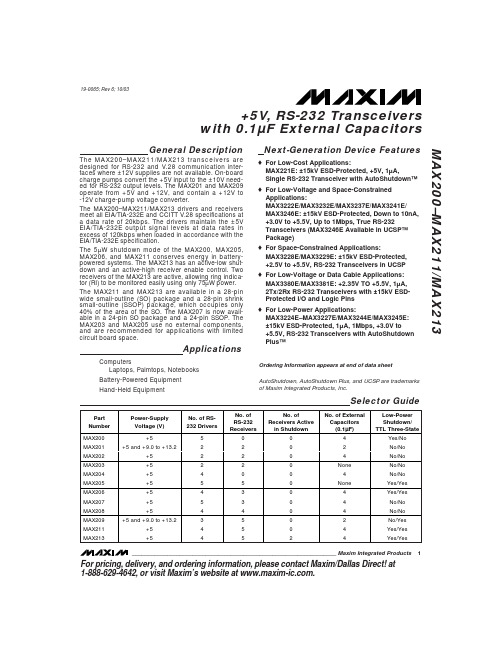
General DescriptionThe MAX200–MAX211/MAX213 transceivers are designed for RS-232 and V.28 communication inter-faces where ±12V supplies are not available. On-board charge pumps convert the +5V input to the ±10V need-ed for RS-232 output levels. The MAX201 and MAX209operate from +5V and +12V, and contain a +12V to -12V charge-pump voltage converter.The MAX200–MAX211/MAX213 drivers and receivers meet all EIA/TIA-232E and CCITT V.28 specifications at a data rate of 20kbps. The drivers maintain the ±5V EIA/TIA-232E output signal levels at data rates in excess of 120kbps when loaded in accordance with the EIA/TIA-232E specification.The 5µW shutdown mode of the MAX200, MAX205,MAX206, and MAX211 conserves energy in battery-powered systems. The MAX213 has an active-low shut-down and an active-high receiver enable control. Two receivers of the MAX213 are active, allowing ring indica-tor (RI) to be monitored easily using only 75µW power.The MAX211 and MAX213 are available in a 28-pin wide small-outline (SO) package and a 28-pin shrink small-outline (SSOP) package, which occupies only 40% of the area of the SO. The MAX207 is now avail-able in a 24-pin SO package and a 24-pin SSOP. The MAX203 and MAX205 use no external components,and are recommended for applications with limited circuit board space.ApplicationsComputersLaptops, Palmtops, Notebooks Battery-Powered Equipment Hand-Held Equipment Next-Generation Device Features ♦For Low-Cost Applications:MAX221E: ±15kV ESD-Protected, +5V, 1µA, Single RS-232 Transceiver with AutoShutdown™♦For Low-Voltage and Space-Constrained Applications:MAX3222E/MAX3232E/MAX3237E/MAX3241E/MAX3246E: ±15kV ESD-Protected, Down to 10nA,+3.0V to +5.5V, Up to 1Mbps, True RS-232Transceivers (MAX3246E Available in UCSP™Package)♦For Space-Constrained Applications:MAX3228E/MAX3229E: ±15kV ESD-Protected,+2.5V to +5.5V, RS-232 Transceivers in UCSP ♦For Low-Voltage or Data Cable Applications:MAX3380E/MAX3381E: +2.35V TO +5.5V, 1µA,2Tx/2Rx RS-232 Transceivers with ±15kV ESD-Protected I/O and Logic Pins ♦For Low-Power Applications:MAX3224E–MAX3227E/MAX3244E/MAX3245E:±15kV ESD-Protected, 1µA, 1Mbps, +3.0V to+5.5V, RS-232 Transceivers with AutoShutdown Plus™MAX200–MAX211/MAX213+5V , RS-232 Transceivers with 0.1µF External Capacitors ________________________________________________________________Maxim Integrated Products 119-0065; Rev 6; 10/03For pricing, delivery, and ordering information,please contact Maxim/Dallas Direct!at 1-888-629-4642, or visit Maxim’s website at .Ordering Information appears at end of data sheetAutoShutdown, AutoShutdown Plus, and UCSP are trademarks of Maxim Integrated Products, Inc.MAX200–MAX211/MAX213+5V , RS-232 Transceiverswith 0.1µF External Capacitors______________________________________________________________________________________19Ordering Information*Contact factory for dice specifications.M A X 200–M A X 211/M A X 213+5V , RS-232 Transceiverswith 0.1µF External Capacitors Maxim cannot assume responsibility for use of any circuitry other than circuitry entirely embodied in a Maxim product. No circuit patent licenses are implied. Maxim reserves the right to change the circuitry and specifications without notice at any time.20____________________Maxim Integrated Products, 120 San Gabriel Drive, Sunnyvale, CA 94086 408-737-7600©2003 Maxim Integrated ProductsPrinted USAis a registered trademark of Maxim Integrated Products.Package Information(The package drawing(s) in this data sheet may not reflect the most current specifications. For the latest package outline information,go to /packages .)。
MAX241EAI+资料
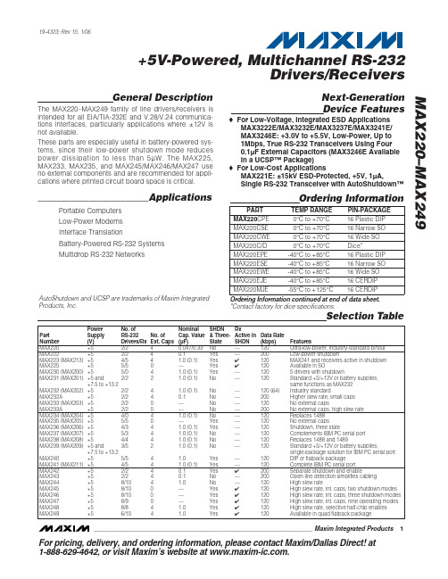
General DescriptionThe MAX220–MAX249 family of line drivers/receivers is intended for all EIA/TIA-232E and V.28/V.24 communica-tions interfaces, particularly applications where ±12V is not available.These parts are especially useful in battery-powered sys-tems, since their low-power shutdown mode reduces power dissipation to less than 5µW. The MAX225,MAX233, MAX235, and MAX245/MAX246/MAX247 use no external components and are recommended for appli-cations where printed circuit board space is critical.________________________ApplicationsPortable Computers Low-Power Modems Interface TranslationBattery-Powered RS-232 Systems Multidrop RS-232 NetworksNext-Generation Device Features♦For Low-Voltage, Integrated ESD ApplicationsMAX3222E/MAX3232E/MAX3237E/MAX3241E/MAX3246E: +3.0V to +5.5V, Low-Power, Up to 1Mbps, True RS-232 Transceivers Using Four 0.1µF External Capacitors (MAX3246E Available in a UCSP™Package)♦For Low-Cost ApplicationsMAX221E: ±15kV ESD-Protected, +5V, 1µA,Single RS-232 Transceiver with AutoShutdown™MAX220–MAX249+5V-Powered, Multichannel RS-232Drivers/Receivers________________________________________________________________Maxim Integrated Products 1Selection Table19-4323; Rev 15; 1/06Power No. of NominalSHDN RxPart Supply RS-232No. of Cap. Value & Three-Active in Data Rate Number (V)Drivers/Rx Ext. Caps (µF)State SHDN (kbps)FeaturesMAX220+52/240.047/0.33No —120Ultra-low-power, industry-standard pinout MAX222+52/2 4 0.1Yes —200Low-power shutdownMAX223 (MAX213)+54/54 1.0 (0.1)Yes ✔120MAX241 and receivers active in shutdown MAX225+55/50—Yes ✔120Available in SOMAX230 (MAX200)+55/04 1.0 (0.1)Yes —120 5 drivers with shutdownMAX231 (MAX201)+5 and2/2 2 1.0 (0.1)No —120Standard +5/+12V or battery supplies; +7.5 to +13.2same functions as MAX232MAX232 (MAX202)+52/24 1.0 (0.1)No —120 (64)Industry standardMAX232A+52/240.1No —200Higher slew rate, small caps MAX233 (MAX203)+52/20— No —120No external capsMAX233A+52/20—No —200No external caps, high slew rate MAX234 (MAX204)+54/04 1.0 (0.1)No —120Replaces 1488MAX235 (MAX205)+55/50—Yes —120No external capsMAX236 (MAX206)+54/34 1.0 (0.1)Yes —120Shutdown, three stateMAX237 (MAX207)+55/34 1.0 (0.1)No —120Complements IBM PC serial port MAX238 (MAX208)+54/44 1.0 (0.1)No —120Replaces 1488 and 1489MAX239 (MAX209)+5 and3/52 1.0 (0.1)No —120Standard +5/+12V or battery supplies;+7.5 to +13.2single-package solution for IBM PC serial port MAX240+55/54 1.0Yes —120DIP or flatpack package MAX241 (MAX211)+54/54 1.0 (0.1)Yes —120Complete IBM PC serial port MAX242+52/240.1Yes ✔200Separate shutdown and enableMAX243+52/240.1No —200Open-line detection simplifies cabling MAX244+58/104 1.0No —120High slew rateMAX245+58/100—Yes ✔120High slew rate, int. caps, two shutdown modes MAX246+58/100—Yes ✔120High slew rate, int. caps, three shutdown modes MAX247+58/90—Yes ✔120High slew rate, int. caps, nine operating modes MAX248+58/84 1.0Yes ✔120High slew rate, selective half-chip enables MAX249+56/1041.0Yes✔120Available in quad flatpack packageFor pricing, delivery, and ordering information,please contact Maxim/Dallas Direct!at 1-888-629-4642, or visit Maxim’s website at .Ordering InformationOrdering Information continued at end of data sheet.*Contact factory for dice specifications.AutoShutdown and UCSP are trademarks of Maxim Integrated Products, Inc.M A X 220–M A X 249+5V-Powered, Multichannel RS-232Drivers/Receivers 2_______________________________________________________________________________________ABSOLUTE MAXIMUM RATINGS—MAX220/222/232A/233A/242/243ELECTRICAL CHARACTERISTICS—MAX220/222/232A/233A/242/243Note 1:For the MAX220, V+ and V- can have a maximum magnitude of 7V, but their absolute difference cannot exceed 13V.Note 2:Input voltage measured with T OUT in high-impedance state, SHDN or V CC = 0V.Note 3:Maximum reflow temperature for the MAX233A is +225°C.Stresses beyond those listed under “Absolute Maximum Ratings” may cause permanent damage to the device. These are stress ratings only, and functional operation of the device at these or any other conditions beyond those indicated in the operational sections of the specifications is not implied. Exposure to absolute maximum rating conditions for extended periods may affect device reliability.Supply Voltage (V CC )...............................................-0.3V to +6V V+ (Note 1)..................................................(V CC - 0.3V) to +14V V- (Note 1).............................................................+0.3V to +14V Input VoltagesT IN ..............................................................-0.3V to (V CC - 0.3V)R IN (Except MAX220)........................................................±30V R IN (MAX220).....................................................................±25V T OUT (Except MAX220) (Note 2).......................................±15V T OUT (MAX220)...............................................................±13.2V Output VoltagesT OUT ...................................................................................±15V R OUT .........................................................-0.3V to (V CC + 0.3V)Driver/Receiver Output Short Circuited to GND.........Continuous Continuous Power Dissipation (T A = +70°C)16-Pin Plastic DIP (derate 10.53mW/°C above +70°C)..842mW18-Pin Plastic DIP (derate 11.11mW/°C above +70°C)..889mW 20-Pin Plastic DIP (derate 8.00mW/°C above +70°C)..440mW 16-Pin Narrow SO (derate 8.70mW/°C above +70°C)...696mW 16-Pin Wide SO (derate 9.52mW/°C above +70°C)......762mW 18-Pin Wide SO (derate 9.52mW/°C above +70°C)......762mW 20-Pin Wide SO (derate 10.00mW/°C above +70°C)....800mW 20-Pin SSOP (derate 8.00mW/°C above +70°C)..........640mW 16-Pin CERDIP (derate 10.00mW/°C above +70°C).....800mW 18-Pin CERDIP (derate 10.53mW/°C above +70°C).....842mW Operating Temperature RangesMAX2_ _AC_ _, MAX2_ _C_ _.............................0°C to +70°C MAX2_ _AE_ _, MAX2_ _E_ _..........................-40°C to +85°C MAX2_ _AM_ _, MAX2_ _M_ _.......................-55°C to +125°C Storage Temperature Range.............................-65°C to +160°C Lead Temperature (soldering, 10s) (Note 3)...................+300°CMAX220–MAX249+5V-Powered, Multichannel RS-232Drivers/Receivers_______________________________________________________________________________________3Note 4:MAX243 R2OUT IN ELECTRICAL CHARACTERISTICS—MAX220/222/232A/233A/242/243 (continued)M A X 220–M A X 249+5V-Powered, Multichannel RS-232Drivers/Receivers 4_________________________________________________________________________________________________________________________________Typical Operating CharacteristicsMAX220/MAX222/MAX232A/MAX233A/MAX242/MAX243108-1051525OUTPUT VOLTAGE vs. LOAD CURRENT-4-6-8-2642LOAD CURRENT (mA)O U T P U T V O L T A G E (V )1002011104104060AVAILABLE OUTPUT CURRENTvs. DATA RATE65798DATA RATE (kb/s)O U T P U T C U R R E N T (m A )203050+10V-10VMAX222/MAX242ON-TIME EXITING SHUTDOWN+5V +5V 0V0V 500μs/div V +, V - V O L T A G E (V )ELECTRICAL CHARACTERISTICS—MAX220/222/232A/233A/242/243 (continued)(V CC = +5V ±10%, C1–C4 = 0.1µF‚ MAX220, C1 = 0.047µF, C2–C4 = 0.33µF, T A = T MIN to T MAX ‚ unless otherwise noted.)MAX220–MAX249+5V-Powered, Multichannel RS-232Drivers/Receivers_______________________________________________________________________________________5V CC ...........................................................................-0.3V to +6V V+................................................................(V CC - 0.3V) to +14V V-............................................................................+0.3V to -14V Input VoltagesT IN ............................................................-0.3V to (V CC + 0.3V)R IN ......................................................................................±30V Output VoltagesT OUT ...................................................(V+ + 0.3V) to (V- - 0.3V)R OUT .........................................................-0.3V to (V CC + 0.3V)Short-Circuit Duration, T OUT ......................................Continuous Continuous Power Dissipation (T A = +70°C)14-Pin Plastic DIP (derate 10.00mW/°C above +70°C)....800mW 16-Pin Plastic DIP (derate 10.53mW/°C above +70°C)....842mW 20-Pin Plastic DIP (derate 11.11mW/°C above +70°C)....889mW 24-Pin Narrow Plastic DIP(derate 13.33mW/°C above +70°C)..........1.07W24-Pin Plastic DIP (derate 9.09mW/°C above +70°C)......500mW 16-Pin Wide SO (derate 9.52mW/°C above +70°C).........762mW20-Pin Wide SO (derate 10.00mW/°C above +70°C).......800mW 24-Pin Wide SO (derate 11.76mW/°C above +70°C).......941mW 28-Pin Wide SO (derate 12.50mW/°C above +70°C) .............1W 44-Pin Plastic FP (derate 11.11mW/°C above +70°C).....889mW 14-Pin CERDIP (derate 9.09mW/°C above +70°C)..........727mW 16-Pin CERDIP (derate 10.00mW/°C above +70°C)........800mW 20-Pin CERDIP (derate 11.11mW/°C above +70°C)........889mW 24-Pin Narrow CERDIP(derate 12.50mW/°C above +70°C)..............1W24-Pin Sidebraze (derate 20.0mW/°C above +70°C)..........1.6W 28-Pin SSOP (derate 9.52mW/°C above +70°C).............762mW Operating Temperature RangesMAX2 _ _ C _ _......................................................0°C to +70°C MAX2 _ _ E _ _...................................................-40°C to +85°C MAX2 _ _ M _ _......................................................-55°C to +125°C Storage Temperature Range.............................-65°C to +160°C Lead Temperature (soldering, 10s) (Note 4)...................+300°CABSOLUTE MAXIMUM RATINGS—MAX223/MAX230–MAX241ELECTRICAL CHARACTERISTICS—MAX223/MAX230–MAX241(MAX223/230/232/234/236/237/238/240/241, V CC = +5V ±10; MAX233/MAX235, V CC = 5V ±5%‚ C1–C4 = 1.0µF; MAX231/MAX239,V CC = 5V ±10%; V+ = 7.5V to 13.2V; T A = T MIN to T MAX ; unless otherwise noted.)Stresses beyond those listed under “Absolute Maximum Ratings” may cause permanent damage to the device. These are stress ratings only, and functional operation of the device at these or any other conditions beyond those indicated in the operational sections of the specifications is not implied. Exposure to absolute maximum rating conditions for extended periods may affect device reliability.Note 4:Maximum reflow temperature for the MAX233/MAX235 is +225°C.M A X 220–M A X 249+5V-Powered, Multichannel RS-232Drivers/Receivers 6_______________________________________________________________________________________ELECTRICAL CHARACTERISTICS—MAX223/MAX230–MAX241 (continued)(MAX223/230/232/234/236/237/238/240/241, V CC = +5V ±10; MAX233/MAX235, V CC = 5V ±5%‚ C1–C4 = 1.0µF; MAX231/MAX239,V CC = 5V ±10%; V+ = 7.5V to 13.2V; T A = T MIN to T MAX ; unless otherwise noted.)MAX220–MAX249+5V-Powered, Multichannel RS-232Drivers/Receivers_______________________________________________________________________________________78.56.54.55.5TRANSMITTER OUTPUT VOLTAGE (V OH ) vs. V CC7.08.0V CC (V)V O H (V )5.07.57.46.02500TRANSMITTER OUTPUT VOLTAGE (V OH )vs. LOAD CAPACITANCE AT DIFFERENT DATA RATES6.46.27.27.0LOAD CAPACITANCE (pF)V O H (V )1500100050020006.86.612.04.02500TRANSMITTER SLEW RATE vs. LOAD CAPACITANCE6.05.011.09.010.0LOAD CAPACITANCE (pF)S L E W R A T E (V /μs )1500100050020008.07.0-6.0-9.04.55.5TRANSMITTER OUTPUT VOLTAGE (V OL ) vs. V CC-8.0-8.5-6.5-7.0V CC (V)V O L (V )5.0-7.5-6.0-7.62500TRANSMITTER OUTPUT VOLTAGE (V OL )vs. LOAD CAPACITANCE AT DIFFERENT DATA RATES-7.0-7.2-7.4-6.2-6.4LOAD CAPACITANCE (pF)V O L (V )150010005002000-6.6-6.810-105101520253035404550TRANSMITTER OUTPUT VOLTAGE (V+, V-)vs. LOAD CURRENT-2-6-4-886CURRENT (mA)V +, V - (V )420__________________________________________Typical Operating CharacteristicsMAX223/MAX230–MAX241*SHUTDOWN POLARITY IS REVERSED FOR NON MAX241 PARTSV+, V- WHEN EXITING SHUTDOWN(1μF CAPACITORS)MAX220-13SHDN*V-O V+500ms/divM A X 220–M A X 249+5V-Powered, Multichannel RS-232Drivers/Receivers 8_______________________________________________________________________________________ABSOLUTE MAXIMUM RATINGS—MAX225/MAX244–MAX249ELECTRICAL CHARACTERISTICS—MAX225/MAX244–MAX249(MAX225, V CC = 5.0V ±5%; MAX244–MAX249, V CC = +5.0V ±10%, external capacitors C1–C4 = 1µF; T A = T MIN to T MAX ; unless oth-erwise noted.)Stresses beyond those listed under “Absolute Maximum Ratings” may cause permanent damage to the device. These are stress ratings only, and functional operation of the device at these or any other conditions beyond those indicated in the operational sections of the specifications is not implied. Exposure to absolute maximum rating conditions for extended periods may affect device reliability.Supply Voltage (V CC )...............................................-0.3V to +6V Input VoltagesT IN ‚ ENA , ENB , ENR , ENT , ENRA ,ENRB , ENTA , ENTB ..................................-0.3V to (V CC + 0.3V)R IN .....................................................................................±25V T OUT (Note 5).....................................................................±15V R OUT ........................................................-0.3V to (V CC + 0.3V)Short Circuit (one output at a time)T OUT to GND............................................................Continuous R OUT to GND............................................................ContinuousContinuous Power Dissipation (T A = +70°C)28-Pin Wide SO (derate 12.50mW/°C above +70°C).............1W 40-Pin Plastic DIP (derate 11.11mW/°C above +70°C)...611mW 44-Pin PLCC (derate 13.33mW/°C above +70°C)...........1.07W Operating Temperature RangesMAX225C_ _, MAX24_C_ _ ..................................0°C to +70°C MAX225E_ _, MAX24_E_ _ ...............................-40°C to +85°C Storage Temperature Range.............................-65°C to +160°C Lead Temperature (soldering,10s) (Note 6)....................+300°CNote 5:Input voltage measured with transmitter output in a high-impedance state, shutdown, or V CC = 0V.Note 6:Maximum reflow temperature for the MAX225/MAX245/MAX246/MAX247 is +225°C.MAX220–MAX249+5V-Powered, Multichannel RS-232Drivers/Receivers_______________________________________________________________________________________9Note 7:The 300Ωminimum specification complies with EIA/TIA-232E, but the actual resistance when in shutdown mode or V CC =0V is 10M Ωas is implied by the leakage specification.ELECTRICAL CHARACTERISTICS—MAX225/MAX244–MAX249 (continued)(MAX225, V CC = 5.0V ±5%; MAX244–MAX249, V CC = +5.0V ±10%, external capacitors C1–C4 = 1µF; T A = T MIN to T MAX ; unless oth-erwise noted.)M A X 220–M A X 249+5V-Powered, Multichannel RS-232Drivers/Receivers 10________________________________________________________________________________________________________________________________Typical Operating CharacteristicsMAX225/MAX244–MAX24918212345TRANSMITTER SLEW RATE vs. LOAD CAPACITANCE86416LOAD CAPACITANCE (nF)T R A N S M I T T E R S L E W R A T E (V /μs )14121010-105101520253035OUTPUT VOLTAGEvs. LOAD CURRENT FOR V+ AND V--2-4-6-88LOAD CURRENT (mA)O U T P U T V O L T A G E (V )64209.05.012345TRANSMITTER OUTPUT VOLTAGE (V+, V-)vs. LOAD CAPACITANCE AT DIFFERENT DATA RATES6.05.58.5LOAD CAPACITANCE (nF)V +, V (V )8.07.57.06.5MAX220–MAX249Drivers/ReceiversFigure 1. Transmitter Propagation-Delay Timing Figure 2. Receiver Propagation-Delay TimingFigure 3. Receiver-Output Enable and Disable Timing Figure 4. Transmitter-Output Disable TimingM A X 220–M A X 249Drivers/Receivers ENT ENR OPERATION STATUS TRANSMITTERSRECEIVERS00Normal Operation All Active All Active 01Normal Operation All Active All 3-State10Shutdown All 3-State All Low-Power Receive Mode 11ShutdownAll 3-StateAll 3-StateTable 1a. MAX245 Control Pin ConfigurationsENT ENR OPERATION STATUS TRANSMITTERS RECEIVERSTA1–TA4TB1–TB4RA1–RA5RB1–RB500Normal Operation All Active All Active All Active All Active 01Normal Operation All Active All Active RA1–RA4 3-State,RA5 Active RB1–RB4 3-State,RB5 Active 1ShutdownAll 3-StateAll 3-StateAll Low-Power Receive Mode All Low-Power Receive Mode 11Shutdown All 3-State All 3-StateRA1–RA4 3-State,RA5 Low-Power Receive ModeRB1–RB4 3-State,RB5 Low-Power Receive ModeTable 1b. MAX245 Control Pin ConfigurationsTable 1c. MAX246 Control Pin ConfigurationsENA ENB OPERATION STATUS TRANSMITTERS RECEIVERSTA1–TA4TB1–TB4RA1–RA5RB1–RB500Normal Operation All Active All Active All Active All Active 01Normal Operation All Active All 3-State All Active RB1–RB4 3-State,RB5 Active 1ShutdownAll 3-StateAll ActiveRA1–RA4 3-State,RA5 Active All Active 11Shutdown All 3-State All 3-StateRA1–RA4 3-State,RA5 Low-Power Receive ModeRB1–RB4 3-State,RA5 Low-Power Receive ModeMAX220–MAX249Drivers/ReceiversM A X 220–M A X 249_______________Detailed DescriptionThe MAX220–MAX249 contain four sections: dual charge-pump DC-DC voltage converters, RS-232 dri-vers, RS-232 receivers, and receiver and transmitter enable control inputs.Dual Charge-Pump Voltage ConverterThe MAX220–MAX249 have two internal charge-pumps that convert +5V to ±10V (unloaded) for RS-232 driver operation. The first converter uses capacitor C1 to dou-ble the +5V input to +10V on C3 at the V+ output. The second converter uses capacitor C2 to invert +10V to -10V on C4 at the V- output.A small amount of power may be drawn from the +10V (V+) and -10V (V-) outputs to power external circuitry (see the Typical Operating Characteristics section),except on the MAX225 and MAX245–MAX247, where these pins are not available. V+ and V- are not regulated,so the output voltage drops with increasing load current.Do not load V+ and V- to a point that violates the mini-mum ±5V EIA/TIA-232E driver output voltage when sourcing current from V+ and V- to external circuitry. When using the shutdown feature in the MAX222,MAX225, MAX230, MAX235, MAX236, MAX240,MAX241, and MAX245–MAX249, avoid using V+ and V-to power external circuitry. When these parts are shut down, V- falls to 0V, and V+ falls to +5V. For applica-tions where a +10V external supply is applied to the V+pin (instead of using the internal charge pump to gen-erate +10V), the C1 capacitor must not be installed and the SHDN pin must be tied to V CC . This is because V+is internally connected to V CC in shutdown mode.RS-232 DriversThe typical driver output voltage swing is ±8V when loaded with a nominal 5k ΩRS-232 receiver and V CC =+5V. Output swing is guaranteed to meet the EIA/TIA-232E and V.28 specification, which calls for ±5V mini-mum driver output levels under worst-case conditions.These include a minimum 3k Ωload, V CC = +4.5V, and maximum operating temperature. Unloaded driver out-put voltage ranges from (V+ -1.3V) to (V- +0.5V).Input thresholds are both TTL and CMOS compatible.The inputs of unused drivers can be left unconnected since 400k Ωinput pullup resistors to V CC are built in (except for the MAX220). The pullup resistors force the outputs of unused drivers low because all drivers invert.The internal input pullup resistors typically source 12µA,except in shutdown mode where the pullups are dis-abled. Driver outputs turn off and enter a high-imped-ance state—where leakage current is typically microamperes (maximum 25µA)—when in shutdownmode, in three-state mode, or when device power is removed. Outputs can be driven to ±15V. The power-supply current typically drops to 8µA in shutdown mode.The MAX220 does not have pullup resistors to force the outputs of the unused drivers low. Connect unused inputs to GND or V CC .The MAX239 has a receiver three-state control line, and the MAX223, MAX225, MAX235, MAX236, MAX240,and MAX241 have both a receiver three-state control line and a low-power shutdown control. Table 2 shows the effects of the shutdown control and receiver three-state control on the receiver outputs.The receiver TTL/CMOS outputs are in a high-imped-ance, three-state mode whenever the three-state enable line is high (for the MAX225/MAX235/MAX236/MAX239–MAX241), and are also high-impedance whenever the shutdown control line is high.When in low-power shutdown mode, the driver outputs are turned off and their leakage current is less than 1µA with the driver output pulled to ground. The driver output leakage remains less than 1µA, even if the transmitter output is backdriven between 0V and (V CC + 6V). Below -0.5V, the transmitter is diode clamped to ground with 1k Ωseries impedance. The transmitter is also zener clamped to approximately V CC + 6V, with a series impedance of 1k Ω.The driver output slew rate is limited to less than 30V/µs as required by the EIA/TIA-232E and V.28 specifica-tions. Typical slew rates are 24V/µs unloaded and 10V/µs loaded with 3Ωand 2500pF.RS-232 ReceiversEIA/TIA-232E and V.28 specifications define a voltage level greater than 3V as a logic 0, so all receivers invert.Input thresholds are set at 0.8V and 2.4V, so receivers respond to TTL level inputs as well as EIA/TIA-232E and V.28 levels.The receiver inputs withstand an input overvoltage up to ±25V and provide input terminating resistors withDrivers/ReceiversTable 2. Three-State Control of ReceiversMAX220–MAX249Drivers/Receiversnominal 5k Ωvalues. The receivers implement Type 1interpretation of the fault conditions of V.28 and EIA/TIA-232E.The receiver input hysteresis is typically 0.5V with a guaranteed minimum of 0.2V. This produces clear out-put transitions with slow-moving input signals, even with moderate amounts of noise and ringing. The receiver propagation delay is typically 600ns and is independent of input swing direction.Low-Power Receive ModeThe low-power receive mode feature of the MAX223,MAX242, and MAX245–MAX249 puts the IC into shut-down mode but still allows it to receive information. This is important for applications where systems are periodi-cally awakened to look for activity. Using low-power receive mode, the system can still receive a signal that will activate it on command and prepare it for communi-cation at faster data rates. This operation conserves system power.Negative Threshold—MAX243The MAX243 is pin compatible with the MAX232A, differ-ing only in that RS-232 cable fault protection is removed on one of the two receiver inputs. This means that control lines such as CTS and RTS can either be driven or left floating without interrupting communication. Different cables are not needed to interface with different pieces of equipment.The input threshold of the receiver without cable fault protection is -0.8V rather than +1.4V. Its output goes positive only if the input is connected to a control line that is actively driven negative. If not driven, it defaults to the 0 or “OK to send” state. Normally‚ the MAX243’s other receiver (+1.4V threshold) is used for the data line (TD or RD)‚ while the negative threshold receiver is con-nected to the control line (DTR‚ DTS‚ CTS‚ RTS, etc.). Other members of the RS-232 family implement the optional cable fault protection as specified by EIA/TIA-232E specifications. This means a receiver output goes high whenever its input is driven negative‚ left floating‚or shorted to ground. The high output tells the serial communications IC to stop sending data. To avoid this‚the control lines must either be driven or connected with jumpers to an appropriate positive voltage level.Shutdown—MAX222–MAX242On the MAX222‚ MAX235‚ MAX236‚ MAX240‚ and MAX241‚ all receivers are disabled during shutdown.On the MAX223 and MAX242‚ two receivers continue to operate in a reduced power mode when the chip is in shutdown. Under these conditions‚ the propagation delay increases to about 2.5µs for a high-to-low input transition. When in shutdown, the receiver acts as a CMOS inverter with no hysteresis. The MAX223 and MAX242 also have a receiver output enable input (EN for the MAX242 and EN for the MAX223) that allows receiver output control independent of SHDN (SHDN for MAX241). With all other devices‚ SHDN (SH DN for MAX241) also disables the receiver outputs.The MAX225 provides five transmitters and five receivers‚ while the MAX245 provides ten receivers and eight transmitters. Both devices have separate receiver and transmitter-enable controls. The charge pumps turn off and the devices shut down when a logic high is applied to the ENT input. In this state, the supply cur-rent drops to less than 25µA and the receivers continue to operate in a low-power receive mode. Driver outputs enter a high-impedance state (three-state mode). On the MAX225‚ all five receivers are controlled by the ENR input. On the MAX245‚ eight of the receiver out-puts are controlled by the ENR input‚ while the remain-ing two receivers (RA5 and RB5) are always active.RA1–RA4 and RB1–RB4 are put in a three-state mode when ENR is a logic high.Receiver and Transmitter EnableControl InputsThe MAX225 and MAX245–MAX249 feature transmitter and receiver enable controls.The receivers have three modes of operation: full-speed receive (normal active)‚ three-state (disabled)‚ and low-power receive (enabled receivers continue to function at lower data rates). The receiver enable inputs control the full-speed receive and three-state modes. The transmitters have two modes of operation: full-speed transmit (normal active) and three-state (disabled). The transmitter enable inputs also control the shutdown mode. The device enters shutdown mode when all transmitters are disabled. Enabled receivers function in the low-power receive mode when in shutdown.M A X 220–M A X 249Tables 1a–1d define the control states. The MAX244has no control pins and is not included in these tables. The MAX246 has ten receivers and eight drivers with two control pins, each controlling one side of the device. A logic high at the A-side control input (ENA )causes the four A-side receivers and drivers to go into a three-state mode. Similarly, the B-side control input (ENB ) causes the four B-side drivers and receivers to go into a three-state mode. As in the MAX245, one A-side and one B-side receiver (RA5 and RB5) remain active at all times. The entire device is put into shut-down mode when both the A and B sides are disabled (ENA = ENB = +5V).The MAX247 provides nine receivers and eight drivers with four control pins. The ENRA and ENRB receiver enable inputs each control four receiver outputs. The ENTA and ENTB transmitter enable inputs each control four drivers. The ninth receiver (RB5) is always active.The device enters shutdown mode with a logic high on both ENTA and ENTB .The MAX248 provides eight receivers and eight drivers with four control pins. The ENRA and ENRB receiver enable inputs each control four receiver outputs. The ENTA and ENTB transmitter enable inputs control four drivers each. This part does not have an always-active receiver. The device enters shutdown mode and trans-mitters go into a three-state mode with a logic high on both ENTA and ENTB .The MAX249 provides ten receivers and six drivers with four control pins. The ENRA and ENRB receiver enable inputs each control five receiver outputs. The ENTA and ENTB transmitter enable inputs control three dri-vers each. There is no always-active receiver. The device enters shutdown mode and transmitters go into a three-state mode with a logic high on both ENTA and ENTB . In shutdown mode, active receivers operate in a low-power receive mode at data rates up to 20kb/s.__________Applications InformationFigures 5 through 25 show pin configurations and typi-cal operating circuits. In applications that are sensitive to power-supply noise, V CC should be decoupled to ground with a capacitor of the same value as C1 and C2 connected as close as possible to the device.Drivers/Receivers。
MAX3420E中断系统(doc13)
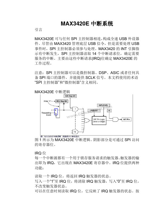
MAX3420E中断系统引言MAX3420E可与任何SPI主控制器相连,构成全速USB外设器件。
尽管由MAX3420管理底层USB信令,但是需要处理USB 事件时,SPI主控制器必须参与处理。
MAX3420的INT引脚指示有中断发生,SPI主控制器读取14个中断请求位,确定需要服务的中断。
主要由这些中断请求(IRQ)位确定MAX3420E的工作过程。
注意:SPI主控制器可以是微控制器、DSP、ASIC或者任何具备SPI端口的器件,并能提供SCLK信号。
本文档使用的术语“SPI主控制器”和“微控制器”含义相同。
MAX3420E中断逻辑图1所示为MAX3420E中断逻辑。
阴影部分是可通过SPI访问的寄存器位。
IRQ位每一个中断源都有一个用于锁存服务请求的触发器。
触发器的输出即为IRQ,它出现在MAX3420E寄存器中。
IRQ位提供两种功能:读取一个IRQ位,将返回IRQ触发器的状态。
写入一个“1”至IRQ位,将清除IRQ触发器,写入“0”至IRQ位,不改变触发器状态。
可以在任意时刻读取IRQ位,它反映了IRQ触发器的状态。
按照上面第2条,写入1而不是0来清除所选的IRQ位,这一过程不需要读-修改-写周期。
举例说明,假设MAX3420E的IRQ 位与普通的寄存器位一样,写1置位,写0清除。
现在,我们想要清除USBIRQ寄存器的URESIRQ位。
图2所示为实现该操作的代码。
由于SPI主控制器通过写1来清除一个MAX3420E IRQ位,而写0不改变其他寄存器位,因此SPI主控制器可以直接写入位屏蔽值来清除URESIRQ位。
所以,图2中的最后三条语句可以由图3中的单条语句替代。
IEN位14个MAX3420E中断的每一个都有相应的中断使能(IEN)位。
IEN位和IRQ触发器输出进行“与”操作,决定是否向INT引脚传送中断请求(图1)。
14个IRQ触发器通过门控电路后,进行“或”操作,形成一个内部中断请求信号,传送至中断引脚逻辑模块。
- 1、下载文档前请自行甄别文档内容的完整性,平台不提供额外的编辑、内容补充、找答案等附加服务。
- 2、"仅部分预览"的文档,不可在线预览部分如存在完整性等问题,可反馈申请退款(可完整预览的文档不适用该条件!)。
- 3、如文档侵犯您的权益,请联系客服反馈,我们会尽快为您处理(人工客服工作时间:9:00-18:30)。
```````````````````````````````````গၤNBY4532F!VTCᅪ0ᓍ૦఼ᒜ۞೫Ⴥᎌܘገࡼၫᔊ൝ਜ਼ෝผ࢟വLjభဣሚ९VTC!3/1ਖपࡼཝႥVTCᅪཝႥ0ࢅႥᓍ૦ăดᒙࡼ၃खᎌ±26lWࡼFTEۣઐLj݀ᄋభܠ߈ࡼVTCೌਜ਼ࣥఎถăดݝࠈቲా༺)TJF*ࠀಯށVTCፇࡼᇼஂLjಿྙތࡇଶዩਜ਼ᔐሣᒮ၂ăNBY4532FಽጙᔝࡀᐱఎᔫLjᄰਭጙৈᔢᔫႥൈࡉ37NI{ࡼTQJ UNాభጲषᆰᑚቋࡀăಽ଼ࡼ4ሣ5ሣTQJాLjকୈభጲྀੜTQJᓍ఼ᒜ)ᆈࠀಯĂBTJDĂETQࢀ*ᐐଝVTCᅪᓍ૦ถăࡩᔫᆐVTCᓍ૦ᔫဟLjNBY4532FဧࡍࡼVTCᅪถ৫ᆐྀੜᆈࠀಯĂBTJDETQჅăጲ࢛ࡵ࢛ऱښᆐಿLjభጲᆐ༊ྜྷါᇹᄻᐐଝVTCၡܪాLjݷᔫNBY4532Fࡼৼୈభጲऻޟ଼Ljፐᆐᒑኊᑽߒৈܪ۸ăᎅ᎖ดݝૹ߅೫࢟ຳᓞધLjTQJాభᔫ᎖2/5Wᒗ4/7Wࡼᇹᄻ࢟ኹăVTCࢾဟݷᔫᏴNBY4532Fดݝᅲ߅Ljᅲ߅ઁᄋᒦࣥLjᑚዹᇄኊᐴTQJᓍ఼ᒜࡼࢾဟ൸ᔗVTCࢾဟገཇăNBY4532Fથᄋڭവᄰၒྜྷਜ਼ၒ߲LjፐࠥLjࡩᆈࠀಯݧJ0P୭ဣሚTQJాဟLjᔐࡼJ0PాሣݙିनᐐăNBY4532Fᔫ᎖.51°Dᒗ,96°D౫ᐱᆨࣞपᆍLj۸ᎌ43୭URGQॖᓤ)6nn y6nn*ਜ਼43୭URGOॖᓤ)6nn y 6nn*ă```````````````````````````````````።```````````````````````````````````ᄂቶ♦ࣖೂ᎖ᆈࠀಯࡼVTCऱښ♦ྟୈରྏ᎖TQJాࡼVTCᅪ఼ᒜNBY4531F♦९VTC!3/1ਖप)ཝႥ23NcqtᅪLjཝ0ࢅႥ23Ncqt02/6Ncqtᓍ૦*♦ૹ߅VTC၃ख♦ৼୈ0፮ୈ఼ᒜดݝE,౯࢟ᔜ)ᅪෝါ*ਜ਼E,0E.ሆ౯࢟ᔜ)ᓍ૦ෝါ*♦భܠ߈4ሣ5ሣ37NI{!TQJా♦࢟ຳᓞધਜ਼W MၒྜྷᏤဧࣖೂࡼᇹᄻా࢟ኹ♦Ᏼᔈ࢟ᅪ።ᒦᎅดݝ܈୷ଶހW CVT♦E,ĂE.ਜ਼WCDPNQᄋFTEۣઐ♦ᒦࣥၒ߲୭)࢟ຳభܠ߈ܟዘ߿खෝါ*ဣሚއኯᒦࣥདࣅࡼTQJా♦ڭৈᄰၒྜྷLjڭৈᄰၒ߲♦᎖ᄰၒྜྷ୭ࡼᒦࣥቧLjభܠ߈ܟዘቶ♦ᒝถVTC!TJF♦ᔈࣅࠀಯVTCഗ఼ᒜਜ਼ၷદࡀ♦ࠀಯށVTCቧᇼஂ♦ᔈࡒࢾဟ൸ᔗVTCࢾဟገཇLjᇄኊTQJᓍ఼ᒜݬᎧࢾဟူୈ♦ஂဏహମࡼᇄURGQਜ਼URGOॖᓤ)6nn!y!6nn*NBY4532FTQJాࡼVTCᅪ0ᓍ૦఼ᒜ19-3953; Rev 3; 7/07༊ྜྷါᇹᄻጛ೦۸ᆈࠀಯਜ਼ETQ ઓVTC۸ሤ૦გါവᎅQMD૦ࢻਫ਼QEBNQ4݃हጥܭ```````````````````````````````ࢾ৪ቧᇦ*FQ!>!ൡLjೌᒗă+ܭာᇄॖᓤăTQJဵNpupspmb-!Jod/ࡼܪă۾ᆪဵNbyjnᑵါ፞ᆪᓾ೯ࡼፉᆪLjNbyjnݙ࣪डፉᒦࡀᏴࡼތፊᎅࠥޘညࡼࡇᇙঌᐊă༿ᓖፀፉᆪᒦభถࡀᏴᆪᔊᔝᒅडፉࡇᇙLjྙኊཀྵཱྀྀੜࠤᎫࡼᓰཀྵቶLj༿ݬఠNbyjnᄋࡼ፞ᆪۈᓾ೯ăჃནॅዹອਜ਼ᔢቤۈࡼၫᓾ೯Lj༿षᆰNbyjnࡼᓍǖxxx/nbyjn.jd/dpn/doă________________________________________________________________Maxim Integrated Products1N B Y 4532F```````````````````````````ᓍ૦ᔫᄂቶ♦ᏴᏇࡼNBY4531Fࡀᔝᒦᐐଝလጙৈࡀ)S32–S42*఼ᒜᓍ૦ᔫෝါ♦ᓍ఼ᒜᔫ᎖ཝႥࢅႥෝါ♦GJGPTOEGJGP;!ख႙GJGPLjၷદߡĂ75ᔊஂSDWGJGP;!၃GJGPLjၷદߡĂ75ᔊஂ♦ࠀಯEBUB10EBUB2߿खࡼޘညਜ਼ଶހ♦ࠀಯཝݝࠅ႙ਭ߈ࡼࡇᇙቅዩ♦ጲ2ntମᔈࣅޘညTPG )ཝႥ*0FPQ )ࢅႥ*♦ಽᑷဪ۞)TPG0FPQ*ᔈࣅᄴݛᓍ૦ࠅ႙♦భۨসᓍ૦༿ཇࡼஉਫ♦ᑽߒVTCૹሣ♦ᑽߒJTPDISPOPVT )ᄴݛ*ࠅ႙♦଼ܠ߈TJFᔈࣅޘညᒲ໐ቶTPG )ཝႥ*FPQ )ࢅႥ*ᑷܪTQJᓍ఼ᒜᓤᏲၫLjᒙถᏄᒍĂ࢛࣡ਜ਼ࠅ႙ಢቯLj݀ࣅࠅ႙NBY4532Fጲᒦࣥਜ਼ࡔ൩ۨসᅪࡼሰ።భᏴྀፀဟମଝᏲࠅ႙༿ཇTJFᎧᑷܪۣߒᄴݛ࣪᎖ࣶ۞ࠅ႙LjTJFᔈࣅᆒઐ݀ଶއၫ߿ख```````````````````````````ᅪᔫᄂቶ♦ดݝ࢛࣡GJGPFQ1ǖ఼ᒜ)DPOUSPM*!)75ᔊஂ*FQ2ǖၒ߲)PVU*LjCVMLJOUFSSVQULj3!y!75ᔊஂ)ၷદߡ*FQ3ǖၒྜྷ)JO*LjCVMLJOUFSSVQULj3!y!75ᔊஂ)ၷદߡ*FQ4ǖၒྜྷ)JO*LjCVMLJOUFSSVQU!)75ᔊஂ*♦ၷદߡၫ࢛࣡ᏤTQJᓍ఼ᒜࡼၫࠅ႙ᎧVTC ࠅ႙ᄴဟቲLjᄋ೫ᅔᅊถೆ♦ᒙ)TFUVQ*ၫᎌᔈࡼ9ᔊஂGJGPLj଼છ೫ৼୈTQJాࡼVTCᅪ0ᓍ૦఼ᒜ2_______________________________________________________________________________________NBY4532Fᄰਭ45ৈా୭ೌᒗྀੜᆈࠀಯ)μQ*)ᅄ2*ă࣪᎖ݙ፮ୈTQJాࡼ଼ᆈࠀಯLjభᄰਭᄰJ0P୭ᓆᆡݷᔫࡼऱါቲᄰቧăNBY4532FࡼڭৈHQJO )ᄰၒྜྷ*୭ਜ਼ڭৈHQPVU )ᄰၒ߲*୭ᄐࡔμQۻᄰቧాᐴࡼాሣઁ྆ᎌăႰNBY4532F ࡼTQJాᎌࣖೂࡼၫၒྜྷ)NPTJLjᓍ߲࠭ྜྷ*ਜ਼ၫၒ߲)NJTPLjᓍྜྷ߲࠭*୭Ljᎅ᎖TQJాࡼNPTJጐభᒙᆐၷሶၫሣLjభጲဏሆጙৈా୭ă૾Ⴥᆣࡼۍၷෝါă```````````````````````````࢜ቯ።࢟വᅄ2/!NBY4532Fᄰਭ45ৈా୭ೌᒗྀੜᆈࠀಯNBY4532FTQJాࡼVTCᅪ0ᓍ૦఼ᒜ_______________________________________________________________________________________3ᅄ3/!NBY4532Fೌᒗࡍቯበຢᅄ4/!ಽNBY4532FဣሚVTCࡼ࢟ಭᅄ5/!NBY4532F᎖༊ྜྷါᓍ૦።NBY4532Fࡼೝৈᄂቶဧऻޟጵ᎖ਜ਼BTJDਜ਼ETQᑚዹࡼࡍਖෝĂႥበຢా)ᅄ3*ă၅ሌLjTQJాࡼႥࣞࡉ37NI{ǗࠨLjࣖࡼW M ୭ਜ਼ดݝ࢟ຳᓞધဧᇹᄻాถ৫ᔫᏴ܈4/4WࡼW DD ৎࢅࡼ࢟ኹăNBY4532FᆐVTCాࡼ࢟ಭᄋ೫ಯሯऱښ)ᅄ4*ăVTCᎌഗ఼ᒜᄂቶLjᏴᆈࠀಯᅲ߅TQJ࣡ాࡼၫࠅ႙ݷᔫ༄LjNBY4532F્ᔈࣅጲOBLᆻ၄۞።ࡊᓍ૦༿ཇăᑚፀᆜᓹTQJాభᔫᏴᔢᒗ37NI{ࡼྀੜຫൈሆăፐࠥLjଐᑗభᔈᎅኡᐋాࡼᔫຫൈLj݀ো߅۾ਜ਼ቶถገཇኡᐋᔢᎁࡼ࢟Ắăᅄ5߲೫NBY4532FᔫᏴVTCᓍ૦ෝါሆࡼᇹᄻౖᅄăVTCᓍ૦።6W࢟ᏎVTC ĐBđቯೌࡼW CVT ୭LjᆐVTCᅪ࢟ăᆐᅪ࢟ࡼᇹᄻኍᏴ࢟୭ݧۣઐ࢟വLjጲᅪਭഗᇹᄻᐆ߅ႼăW CVT ఎਈ)ಿྙNBY589:*భᄋൈ఼ᒜਜ਼ᅪೝሲถǖሢᒜၒ႙ᅪࡼ࢟ഗ)ಿྙ311nB*Lj݀ሶTQJᓍ఼ᒜۨস৺ᑇ)ਭഗ*ăNbyjnᄋࣶᒬݙᄴሢᒜ࢟ഗਜ਼ถࡼW CVT ఎਈăሮ༽༿षᆰNbyjnᆀᐶă4/4Wࢯஂ)ಿྙNBY745:UM*ᆐNBY4532Fᑗᇹᄻ఼ᒜᄋ࢟Ꮞăྙਫᇹᄻ఼ᒜᔫᏴৎࢅ࢟ኹሆLjNBY4532FࡼTQJਜ਼J0PాጐభᔫᏴৎࢅ࢟ኹሆLjᒑኊᇹᄻ࢟ኹ)ಿྙ3/6W2/9W*ೌᒗNBY4532FࡼW M ୭ă````````````````````````````````````````````````````````````````````࢜ቯ።࢟വ)ኚ*N B Y 4532FTQJాࡼVTCᅪ0ᓍ૦఼ᒜ``````````````````````````````````````````````````````````````````````````ถౖᅄNBY4532FTQJాࡼVTCᅪ0ᓍ૦఼ᒜ_______________________________________________________________________________________5``````````````````````````````````````````````````````````````````````````୭ႁීN B Y 4532FTQJాࡼVTCᅪ0ᓍ૦఼ᒜ6_______________________________________________________________________________________````````````````````````````````````````````````````````````````````````````୭ႁී)ኚ*NBY4532FTQJాࡼVTCᅪ0ᓍ૦఼ᒜ_______________________________________________________________________________________7ࡀႁීTQJᓍ఼ᒜᄰਭࣗቖNBY4532Fดݝࡼ37ৈࡀ)ᅪෝါLjܭ2*34ৈࡀ)ᓍ૦ෝါLjܭ3*఼ᒜᔫăᒙᆡNPEFࡀ)S38*ᒦࡼIPTUᆡభᒙNBY4532F ᆐᓍ૦ᔫෝါăࡩᔫᆐVTCᅪဧဟLjNBY4532Fࡼࡀରྏ᎖NBY4531FLjএଝถ᎖ܭ2ሆෂࡼᓖျ2cᒦăਈ᎖ᑚቋࡀดྏࡼᅲᑳႁීLjݬNbyjnᆀᐶࡼ።܊4896ǖNBY4532Fܠ߈ᒎฉăጙࠨࡀषᆰ۞ೝৈࣤLj၅ሌဵTQJᓍ఼ᒜቖTQJ ෘഎᔊஂLjஜᓹဵ࣪ჅኰᒍࡀࡼࣗቖݷᔫăჅᎌTQJࠅ႙࣒ဵNTC )ᔢᎌᆡ*Ᏼሌăෘഎᔊஂ۞౪ࡀᒍĂጙৈऱሶᆡ)ࣗ>1Ljቖ>2*ਜ਼BDLTUBUᆡ)ᅄ6*ăTQJᓍ఼ᒜᏴෘഎᔊஂࡼSfh5ᒗSfh1ᆡቖྜྷࡀܠ࣪።ࡼऔᒜ൩Lj૾భኰᒍ࣪።ࡼNBY4532FดݝࡀăಿྙLjገषᆰJPQJOT2ࡀ)S31*LjSfh5ࡵSfh1భᒙྙሆǖSfh5>2LjSfh4>1LjSfh3>2LjSfh2>1LjSfh1>1ăEJS )ऱሶ*ᆡࢾၫࠅ႙ࡼऱሶăEJS >2ፀᆜᓹၫۻቖྜྷࡀLjEJS >1ፀᆜᓹၫۻ߲ࣗࡀăBDLTUBUᆡࢾFQTUBMMTࡀ)S:*ᒦBDLTUBUᆡࡼᓨზ)ஞ᎖ᅪෝါ*ăTQJᓍ఼ᒜকᆡᒙᆡܭීጯᅲ߅ጙࠨDPOUSPMࠅ႙ăᎅ᎖কᆡ્ۻຫथࡵLjहᏴTQJ ෘഎᔊஂᒦభᄋৼୈൈăᓍ૦ෝါሆBDLTUBUᆡۻăᏴཝၷTQJෝါᒦLjۋႲᓹෘഎᔊஂࡼ႙ྜྷLjNBY4532Fᄴဟ႙߲ڭৈVTCᓨზᆡ)ᅄ7Ă8*ăᏴۍၷෝါᒦLjభږᑍषᆰጙۅࡀᆡࡼऱါषᆰᑚቋᓨზᆡă༄ᇋৈࡀ)S1–S5*षᆰᅪਜ਼ᓍ૦ෝါሆࡼGJGPăᒮআषᆰᑚቋࡀဟดݝࡀᒍۻࣉஉLjᑚዹLjభጲᏴᄴጙৈTQJषᆰᒲ໐ᒦ)SS ۣߒᆐࢅ*ᄰਭGJGPቖྜྷ߲ࣶࣗৈᔊஂăषᆰࡀS6–S2:ဟLjᏴጙࠨTQJषᆰᒲ໐ᒦႲᓹඛৈᔊஂࡼࠅ႙LjดݝࡀᒍభᔈࣅᐐăषᆰS31ဟLjᒍࣉஉ᎖কࡀLjऎ࣪᎖S32–S42ࡼषᆰጐ્ဧดݝᒍᐐLjᒮআषᆰS42ဟᒍࣉஉ᎖S42ăܭ2ਜ਼ܭ3ᒦࡼࡀ፯ስ߲೫ᅪਜ਼ᓍ૦ෝါሆးࡼࡀᆡăݙး᎖෭ᒬෝါࡼࡀᆡመာᆐഃăᑚቋࡀᆡ߲ࣗဟᆐഃLjݙ።ඣቖᆐ൝2ăᅪෝါࡀ፯ስࡩᔫ᎖VTCᅪෝါဟ)NBY4532FࡼIPTUᆡۻᒙ1)෦ཱྀ**LjNBY4532FۣߒᎧNBY4531FࡀࡼରྏቶăᆐNBY4531FቖࡼৼୈᇄኊࢯᑳభᏥቲ᎖NBY4532Făᆐ೫ᑽߒNBY4532FࡼቤᄂቶLjࡀᔝᒦ۞೫ጙቋቤࡼᆡLjᏴܭ2ݝࡼᓖျ2cᒦᎌჅහၤăᓍ૦ෝါࡀ፯ስᑵྙܭ3ჅာLjᏴᓍ૦ෝါሆ)IPTU >2*LjᎌቋNBY4531F ࡀۻᒮቤෘ)ಿྙS2ܤᆐSDWGJGP*Ljᎌቋᎌဧ)መာᆐഃ*Ljऎᎌቋ྆း᎖ᓍ૦ෝါăࠥᅪLjᎌ22ৈࡀ)S32–S42*ᐐଝ೫VTCᓍ૦ถăᅄ8/!ᓍ૦ෝါሆLjVTCᓨზᆡႲᓹඛࠨࠅ႙ࡼ၅ৈᔊஂ႙߲)ཝၷෝါ**BDLTUBUᆡᏴᓍ૦ෝါሆۻăᅄ6/!TQJෘഎᔊஂᅄ7/!ᅪෝါሆLjVTCᓨზᆡႲᓹඛࠨࠅ႙ࡼ၅ৈᔊஂ႙߲)ཝၷෝါ*N B Y 4532FTQJాࡼVTCᅪ0ᓍ૦఼ᒜ8_______________________________________________________________________________________ܭ2/!ᅪෝါሆ)IPTU >1*ࡼNBY4532Fࡀ፯ስ)ᓖ2bĂ2c*ᓖ2bǖbdd!)षᆰ*ܭာTQJᓍ఼ᒜषᆰࡀࡼऱါăS!>!ࣗǗSD!>!༹ࣗ߹ǗSTD!>!ࣗĂᒙᆡ༹߹ă࣪S )ᒑࣗ*ࡀቖݙ્ᎌྀੜᔫă࣪SDᆡ)༹ࣗ߹*ቖ2༹߹কᆡă࣪SDᆡቖഃݙ્ᎌྀੜᔫăNBY4532FTQJాࡼVTCᅪ0ᓍ૦఼ᒜᓖ2cǖᅪෝါሆLjNBY4532F߹೫ሆᐐ༓ถᅪLjᒊቲᎧNBY4531Fሤᄴࡼถǖ2*!S27ቤᐐQVMTFXJE1ਜ਼QVMTFXJE2ᆡ఼ᒜܟዘᒦࣥෝါሆࡼJOU൴ߡࣞ)ᅄ23*ăNBY4531Fᒦᑚቋᆡ෦ཱྀᒙᆐ21/7μtă3*!S32ቤᐐ႐ৈHQJPᆡă4*!S33ਜ਼S34ᄗଝᄰၒྜྷ୭ᒗᒦࣥᇹᄻăS35఼ᒜܟዘቶă5*!S38఼ᒜᅪ0ᓍ૦ෝါਜ਼TFQJSRᆡă6*!ࡩᆡ\HQYC;HQYB^>\2;1^༦ᆡTFQJSR >2!)S385ᆡ*ဟLjHQYၒ߲ࡼCVTBDUቧۻᄐધᆐऔৈJSRቧLjᓜ᎖HQJO୭ޘညᒦࣥăܭ3/!ᓍ૦ෝါሆ)IPTU >2*ࡼNBY4532Fࡀ፯ስ)ᓖ3*ܭ2/!ᅪෝါሆ)IPTU >1*ࡼNBY4532Fࡀ፯ስ)ᓖ2bĂ2c*!)ኚ*N B Y 4532FTQJాࡼVTCᅪ0ᓍ૦఼ᒜ10______________________________________________________________________________________``````````````````````````````````````````````````````````````````````````୭ᒙᓖ3ǖbdd!)षᆰ*ܭာTQJᓍ఼ᒜषᆰࡀࡼऱါăS!>!ࣗǗSD!>!༹ࣗ߹ǗSTD!>!ࣗĂᒙᆡ༹߹ǗMT!>!ଝᏲଶހă࣪S )ᒑࣗ*ࡀቖݙ્ᎌྀੜᔫă࣪SDᆡ)༹ࣗ߹*ቖ2༹߹কᆡă࣪SDᆡቖഃݙ્ᎌྀੜᔫăቖMTࡀ᎖ࡀดྏࣅጙࠨᓍ૦ݷᔫăܭ3/!ᓍ૦ෝါሆ)IPTU >2*ࡼNBY4532Fࡀ፯ስ)ᓖ3*!)ኚ*NBY4532FTQJాࡼVTCᅪ0ᓍ૦఼ᒜABSOLUTE MAXIMUM RATINGSELECTRICAL CHARACTERISTICS)W DD >!,4W!up!,4/7W-!W M >!,2/5W!up!,4/7W-!U B >!U NJO up!U NBY -!vomftt!puifsxjtf!opufe/!Uzqjdbm!wbmvft!bsf!bu!W DD >!,4/4W-!W M >!,3/6W-U B >!,36°D/*!)Opuf!4*Stresses beyond those listed under “Absolute Maximum Ratings” may cause permanent damage to the device. These are stress ratings only, and functional operation of the device at these or any other conditions beyond those indicated in the operational sections of the specifications is not implied. Exposure to absolute maximum rating conditions for extended periods may affect device reliability.(All voltages referenced to GND, unless otherwise noted.)V CC .........................................................................-0.3V to +4V V L .............................................................................-0.3V to +4V VBCOMP .................................................................-0.3V to +6V D+, D-, XI, XO ............................................-0.3V to (V CC + 0.3V)SCLK, MOSI, MISO, SS , RES , GPOUT7–GPOUT0,GPIN7–GPIN0, GPX, INT ..........................-0.3V to (V L + 0.3V)Continuous Power Dissipation (T A = +70°C)32-Pin TQFN (derate 21.3mW/°C above +70°C).......1702mW 32-Pin TQFP (derate 13.1mW/°C above +70°C)........1047mW Operating Temperature Range ...........................-40°C to +85°C Junction Temperature......................................................+150°C Storage Temperature Range.............................-65°C to +150°C Lead Temperature (soldering, 10s).................................+300°CN B Y 4532FTQJాࡼVTCᅪ0ᓍ૦఼ᒜELECTRICAL CHARACTERISTICS (continued))W DD >!,4W!up!,4/7W-!W M >!,2/5W!up!,4/7W-!U B >!U NJO up!U NBY -!vomftt!puifsxjtf!opufe/!Uzqjdbm!wbmvft!bsf!bu!W DD >!,4/4W-!W M >!,3/6W-U B >!,36°D/*!)Opuf!4*NBY4532FTQJాࡼVTCᅪ0ᓍ૦఼ᒜNote 3:Parameters are 100% production tested at T A = +25°C. Specifications over temperature are guaranteed by design.Note 4:Guaranteed by bench testing. Limits are not production tested.Note 5:At V L = 1.4V to 2.5V, derate all the SPI timing characteristics by 50%. Not production tested.Note 6:The minimum period is derived from SPI timing parameters.Note 7:Time-to-exit suspend is dependent on the crystal used.TIMING CHARACTERISTICS)W DD >!,4W!up!,4/7W-!W M >!,2/5W!up!,4/7W-!U B >!U NJO up!U NBY -!vomftt!puifsxjtf!opufe/!Uzqjdbm!wbmvft!bsf!bu!W DD >!,4/4W-!W M >!,3/6W-U B >!,36°D/*!)Opuf!4*N B Y 4532FTQJాࡼVTCᅪ0ᓍ૦఼ᒜ``````````````````````````````````````````````````````````````````ހ၂࢟വਜ਼ဟኔᅄᅄ9/!ဍਜ਼ሆଢ଼ဟମᅄ:/!E,0E.ୣഗހဟࡼঌᏲ༽ౚᅄ22/!TQJᔐሣဟኔᅄ)ۍၷෝါLjTQJෝါ)1-1**ᅄ21/!TQJᔐሣဟኔᅄ)ཝၷෝါLjTQJෝါ)1-1**NBY4532FTQJాࡼVTCᅪ0ᓍ૦఼ᒜ``````````````````````````````````````````````````````````````````````࢜ቯᔫᄂቶ(V CC = +3.3V, V L = +3.3V, T A = +25°C.)```````````````````````````````ሮᇼႁීNBY4532F۞೫ဣሚVTC 3/1ܪᓰཝႥVTCᅪཝ0ࢅႥᓍ૦ჅኊࡼჅᎌၫᔊ൝ਜ਼ෝผ࢟വăᄰਭቖNPEFࡀ)S38*ᒦࡼIPTUᆡLjభጲኡᐋNBY4532FᔫᏴᓍ૦ᅪऱါăNBY4532FดᒙᎌVTC၃खLj݀ᏴE,ĂE.ਜ਼WCDPNQ୭ૹ߅೫±26lWࡼFTEۣઐăE,ሣૹ߅೫భ༤ધࡼ2/6l Ω౯࢟ᔜLjE,ਜ਼E.ሣૹ߅೫భ༤ધࡼ26l Ωሆ౯࢟ᔜăྀੜTQJᓍ఼ᒜ࣒భᄰਭTQJ࠭ୈాᎧNBY4532Fᄰቧ)ᔫ᎖TQJෝါ)1-1*)2-2**ăTQJᓍ఼ᒜᄰਭࣗቖNBY4532Fดݝࡼࡀ࣪ቲषᆰăገᅲ߅ጙࠨ࢜ቯࡼၫࠅ႙Lj၅ሌኊገቖጙৈᔊஂࢾࡀᒍਜ਼ࠅ႙ऱሶLjઁဵገ߲ࣗቖྜྷܪࡀดݝGJGPࡼၫᔊஂăᏴᅪෝါሆLjNBY4532F۞495ᔊஂࡼ࢛࣡દߡࡀLj᎖ጲሆ࢛࣡ǖ•FQ1ǖ75ᔊஂࡼၷሶDPOUSPM࢛࣡•FQ2ǖ3!y!75ᔊஂࡼၷદࡀCVML0JOU!PVU࢛࣡•FQ3ǖ3!y!75ᔊஂࡼၷદࡀCVML0JOU!JO࢛࣡•FQ4ǖ75ᔊஂCVML0JOU!JO࢛࣡ኡᐋFQ2ĂFQ3ĂFQ4ᔫᆐCVMLથဵJOUFSSVQU࢛࣡Ljᅲཝན᎖ඒਭ߈ᒦTQJᓍ఼ᒜऩૄVTCᓍ૦ࡼ࢛࣡හၤ९ăᏴᓍ૦ෝါሆLjNBY4532F۞367ᔊஂࡼख႙ਜ਼၃GJGPࡀǖ•TOEGJGPǖख႙GJGP —ၷદߡ75ᔊஂGJGP •SDWGJGPǖ၃GJGP —ၷદߡ75ᔊஂGJGPᓍ૦GJGPถ৫ጲཝႥࢅႥሶᅪख႙TFUVQĂCVMLĂJOUFSSVQUਜ਼JTPDISPOPVT༿ཇăNBY4532Fถ৫ฃᒇྜྷᄰਭVTCૹሣྜྷࡼࢅႥ۸ăᎅ᎖ࡍݝॊดݝಯྀᇗᎅNBY4532Fᅲ߅Ljܠ߈ऻޟྏጵăTQJ ᓍ఼ᒜᔫᆐጙৈ࢜ቯᓍ૦ࡼݷᔫ଼છᆐǖᒙ۸ᒍਜ਼࢛࣡Ljख႙ጙৈ۞݀ࢀࡗܭීᅲ߅ࡼᒦࣥăઁଶއࠅ႙உਫܪᒔᆡጲཀྵࢾᅪࡼሰ።ăᔈࣅည߅ᑷܪဤ)ཝႥTPG۞ࢅႥۣߒ൴ߡ*Lj݀Ᏼሤ࣪᎖ᑚቋܪᒔࡩࡼဟరॊख۞ăNBY4532Fࡼࡀᔝਜ਼TQJాږᑍଢ଼ࢅTQJᄰቧࡼܪቲ೫ᎁછăࡩኊገTQJᓍ఼ᒜᄋVTCॲᇗဟLjᒦࣥၒ߲JOUሶख߲ቧLjಿྙࡩᎌ۞ࡵࡉĂᎌ۞ख߲ᓍ૦ਂૂআᔐሣࣅဟăၷદߡGJGPᏤVTCਜ਼TQJాᄴဟࠅ႙ၫLjᎌᓐ᎖ۣᑺࡒăEYE DIAGRAMM A X 3421E t o c 01410-1102030405060708023TIME (ns)D + A N D D - (V )N B Y 4532FW DDဗଝ4/4W࢟Ꮞ᎖W DD LjጲདࣅVTC၃खਜ਼ၫᔊ൝ᔫăణதW DD ୭Ljጙᒑ2/1μGࡼჿࠣ࢟ྏവW DD ࡵHOEăW MW M ဵTQJాਜ਼Ⴥᎌၫᔊၒྜྷૺၒ߲ࡼݬఠ࢟ຳăభW M ೌࡵᇹᄻࡼ൝࢟Ꮞăᎅ᎖ดݝ࢟ຳᓞધਜ਼W M ୭ࡼࡀᏴLjTQJాਜ਼Ⴥᎌᄰၒྜྷૺၒ߲ถ৫ᔫᏴ2/5Wᒗ4/7Wࡼᇹᄻ࢟ኹሆăWCDPNQNBY4532Fดݝૹ߅೫ጙৈVTC W CVT ଶހLjWCDPNQ ဵকଶހࡼၒྜྷăWCDPNQ୭భߌ၊ࡉ7Wࡼၒྜྷ࢟ኹăጙᒑ2/1μG ჿࠣ࢟ྏവWCDPNQ ࡵHOEăWCDPNQᏴበຢดݝۻೌᒗጙৈ࢟ኹ܈୷LjጲܣTQJ ᓍ఼ᒜଶހ)ᄰਭᒦࣥއኯࡀᆡ*!W CVT ࡼଝ࢟༽ౚăWCDPNQݙᔫᆐྀੜNBY4532Fดݝ࢟വࡼ࢟ᏎăWCDPNQᄰਭS JO ሆ౯ᒗ)Fmfdusjdbm!Dibsbdufsjtujdt *ăᅪෝါሆࡼWCDPNQWCDPNQᏴበຢดݝۻೌᒗጙৈ࢟ኹ܈୷LjጲܣTQJ ᓍ఼ᒜଶހW CVT ࡼଝ࢟༽ౚăোVTC!3/1ਖपLjᔈ࢟ࡼVTC۸ᏴVTCᓍ૦ਈܕW CVT ࢟ᏎઁLjܘኍ༤ࣥE,ࡼ2/6l Ω౯࢟ᔜăಽVTCDUM ࡀ)S26*ᒦࡼWCHBUFᆡLjNBY4532Fดݝ൝భጲኡᐋᔈࣅ༤ࣥE,ࡼ2/6l Ω౯࢟ᔜăVTCDUMࡀ)S26*ᒦࡼWCHBUFਜ਼DPOOFDUᆡLjᏳଝWCDPNQ܈୷ࡼၒ߲)WCVT`EFU*Ljྯᑗৢᄴ఼ᒜᓹᑚৈW DD ਜ਼E,ମࡼ౯࢟ᔜLjྙܭ4ਜ਼ถౖᅄჅာăᓖፀLjྙਫWCHBUF >2༦WCVT`EFU >1Ljกඐᇄ൙DPOOFDUᆡࡼᒙྙੜLj౯࢟ᔜ્࣒ۻࣥఎăྙਫNBY4532FჅᏴࡼ۸ဵᎅᔐሣ࢟ࡼ)ᄰਭೌᒗW DD ࡼ,4/4Wᆮኹ*LjNBY4532FࡼWCDPNQၒྜྷభᔫᆐᄰၒྜྷဧăᎌਈᑚᒬजࡼሮ༽༿።ቧᇦݝॊăᓍ૦ෝါሆࡼWCDPNQNBY4532FᏴᓍ૦ෝါဟᇄኊଶހW CVT ᓨზăᏴࠥ༽ౚሆLjWCDPNQၒྜྷభᔫᆐᄰၒྜྷဧăE,ਜ਼E.ดݝVTCཝ0ࢅႥ၃खᄰਭၷሶၫ୭E,ਜ਼E.߲ăᑚቋ୭ૹ߅೫±26lW FTEۣઐăE,ਜ਼E.።ᄰਭ44Ω±2&ࠈೊ࢟ᔜೌࡵĐCđቯVTCೌăᅪෝါሆࡼE,ਜ਼E.ᅪෝါሆE,ਜ਼E.ᄰਭࠈೊ࢟ᔜೌࡵĐCđቯVTCೌăభ༤ધࡼ2/6l Ω౯࢟ᔜᏴበຢดݝೌᒗE,ăᓍ૦ෝါሆࡼE,ਜ਼E.ᓍ૦ෝါሆE,ਜ਼E.ᄰਭࠈೊ࢟ᔜೌࡵĐBđቯVTCೌăభ༤ધࡼ26l Ωሆ౯࢟ᔜᏴበຢดݝೌᒗE,ਜ਼E.ăNPEFࡀ)S38*ᒦࡼEQQVMMEOਜ਼ENQVMMEOᆡ఼ᒜᓹE,ਜ਼E.ࡵHOEᒄମࡼೌăᔫᆐᓍ૦ဧဟLjᑚቋᆡᆐ2Ljᄰሆ౯࢟ᔜăࡩᎌᅪۻྜྷގ߹ဟLjᓍ૦ᒦࣥᆡDPOOJSRభሶTQJᓍ఼ᒜख߲সவăYJਜ਼YPYJਜ਼YP୭ጙৈᅪݝࡼ23NI{ᄏೌᒗดݝᑩ࢟വăYJဵᄏᑩࡼၒྜྷLjYPဵၒ߲ă23NI{±1/36&ࡼ݀ೊቕᑩᄏࡼጙ࣡ೌᒗYJLjጙ࣡ᒗYPăᏴYJਜ਼YP࣪ೌঌᏲ࢟ྏ)ᔢࡍ31qG*ăጐభጙৈᅪݝࡼ23NI{±1/36&ဟᒩདࣅYJăྙਫᅪݝဟᒩདࣅYJLjᐌॳహYPăᅪݝဟᒩܘኍ൸ᔗFmfdusjdbm Dibsbdufsjtujdt ܭᒦჅහၤࡼ࢟ኹᄂቶăดݝ൝ဵዘ߿खࡼăᅪݝဟᒩ።কᎌܪ߂61&ࡼᐴహ܈ăTQJాࡼVTCᅪ0ᓍ૦఼ᒜNBY4532FSFT དࣅRESᆐࢅభ߿खNBY4532Fࡼበຢআᆡăበຢআᆡ߹QJODUM)S28*ĂVTCDUM)S26*ਜ਼TQJ൝ᒄᅪࡼჅᎌࡀᒙᆐᔈࡼ෦ཱྀᓨზăበຢআᆡ໐ମჅᎌGJGPࡼดྏᆚᒀăདࣅRESᆐ࢟ຳభဧNBY4532FᅙಭበຢআᆡăRES൴ߡᔢభᒗ311otăਈ᎖NBY4532FࡼআᆡᄂቶݬୈআᆡݝॊăJOU ࡩᎌVTCူୈखညLjኊገTQJᓍ఼ᒜᓖፀဟLjNBY4532F ᄰਭJOUၒ߲୭ख߲ᒦࣥቧăથభጲJOUᒙᆐࡩᎌྀੜᄰၒྜྷ)HQJO1–HQJO8*ۻ߿खဟ)ሮ༽༿HQJO8–HQJO1ݝॊ*ख߲ᒦࣥăTQJᓍ఼ᒜܘኍDQVDUMࡀ)S27*ᒦࡼJFᆡᒙᆡऱభ૮JOUถăྦJFᆡۻ༹ഃLjJOUݙᔫ)࢟ຳෝါሆᆐఎവLjঌዘෝါᆐLjᑵዘෝါᆐࢅ*ăJOUᏴ࢟ጟဪበຢআᆡઁጐࠀ᎖ݙᔫᓨზ)JF>1*ăJOU୭భጲᒙᆐᅎᅴါധఎവၒ߲ăᒙᆡQJODUM ࡀ)S28*ᒦࡼJOUMFWFMᆡభJOUܠ߈ᆐࢅ࢟ຳᎌࡼധఎവၒ߲ăᑚᒬᒙኊገᅪݝࡵW Mࡼ౯࢟ᔜăᏴ࢟ຳෝါሆLjྦᎌྀੜᒦࣥܪᒔۻᒙᆡLjNBY4532F્དࣅJOUᆐࢅăྙਫᎌࣶৈᒦࣥᆚࠀಯLjᐌJOUᒑᎌᏴTQJᓍ఼ᒜ༹߹೫ᔢઁጙৈᎌࡼᒦࣥ༿ཇઁݣ્ܤᆐᇄ)ᅄ23*ăᏴ࢟ຳෝါሆLjQJODUMࡀ)S28*ᒦࡼQPTJOUᆡ࣪᎖JOUᎌᔫă༹ഃJOUMFWFMᆡᐌJOUܠ߈ᆐܟዘෝါࡼᅎᅴါၒ߲ăᄰਭQJODUMࡀ)S28*ᒦࡼQPTJOUᆡభܠ߈ࢾᎌዘăᏴܟዘෝါᒦLjྦᎌᒦࣥ༿ཇखညLjᑗ෭ৈᒦࣥ༿ཇጯۻ༹߹Ljࡣ྆ࡀᏴჇᆚࠀಯࡼᒦࣥ༿ཇLjNBY4532F્ޘညጙৈݬᑍ᎖W Mࡼᄢܤዘ)ᅄ23*ăᏴQJODUMࡀ)S28*ᒦᒙᆡQPTJOUᆡᐌኡᐋJOUᆐဍዘᎌLj༹ഃQPTJOUᆡᐌኡᐋሆଢ଼ዘᎌJOUăDQVDUMࡀ)S27*ᒦࡼQVMTFXJE2ਜ਼QVMTFXJE1ᆡభ఼ᒜܟዘෝါሆJOU൴ߡࡼࣞLjྙܭ5ჅာăHQJO8–HQJO1 TQJᓍ఼ᒜᄰਭࣗནࡀJPQJOT2)S31*ࡼ8ᆡࡵ5ᆡݧዹHQJO4–HQJO1ࡼᓨზăHQJO8–HQJO5ࡼᓨზᄰਭࣗནࡀJPQJOT3)S32*ࡼ8ᆡࡵ5ᆡቲݧዹăሶᑚቋᆡቖၫݙ્ᎌྀੜᔫăᇄ൙ᅪਜ਼ᓍ૦ෝါLj࣒ᎅྯৈࡀ఼ᒜᔈ᎖HQJO8–HQJO1ࡼڭৈᒦࣥ༿ཇăࡀHQJOJSR)S33*ᎌڭৈHQJOၒྜྷࡼᒦࣥ༿ཇܪᒔăࡀHQJOJFO)S34*ᎌڭৈHQJOᒦࣥᔈࣖೂࡼᒦࣥဧถᆡăࡀHQJOQPM )S35*఼ᒜᓹڭৈHQJOᒦࣥࡼܟዘቶăڭৈHQJOᒦࣥۻଝྜྷNBY4532FᒦࣥᇹᄻᒦLjࡩᎌဧถᒦࣥۻ߿खဟLj૾భ࠭JOUၒ߲୭ख߲ᒦࣥቧăથభጲHQJOᒦࣥॊಭ߲LjࣖᄰਭHQY୭ၒ߲LjᒑኊᒙTFQJSR>2૾భăᑚዹభጲିቃᒦࣥॲᇗࡼዓߕLjፐᆐHQYၒ߲ࡼᒦࣥᏎဵጯᒀࡼLjᒑኊއኯHQJOJSRࡀܣభཀྵࢾᒦࣥᏎăᓖፀHQJOQPMᒦࡼᆡ఼ᒜဧดݝĐᆚࠀಯᒦࣥđ߿खᒙᆡࡼHQJOᄢܤዘLjऎऻJOUၒ߲ăJOU୭ࡼၒ߲ᄂቶ၊఼᎖JOUMFWFMਜ਼QPTJOUࡀᆡLjᑵྙNBY4531FጙዹăࡩHQY୭ۻᒙ߅HQJO JOUဟLjၒ߲ᄂቶਜ਼JOU୭ጙዹăᅄ23/!ݙᄴJOUMFWFMਜ਼QPTJOUᆡᒙဟJOU୭ࡼܭሚTQJాࡼVTCᅪ0ᓍ૦఼ᒜN B Y 4532FTQJాࡼVTCᅪ0ᓍ૦఼ᒜHQPVU8–HQPVU1TQJᓍ఼ᒜᄰਭቖࡀJPQJOT2)S31*ࡼ4ᆡࡵ1ᆡ఼ᒜHQPVU4–HQPVU1ࡼᓨზăHQPVU8–HQPVU5ࡼᓨზభᄰਭቖࡀJPQJOT3)S32*ࡼ4ᆡࡵ1ᆡቲ఼ᒜăHQPVU8–HQPVU1ࡼ൝࢟ຳጲW M ࢟ኹᆐݬఠăྙᅄ24ჅာLjᏴࣗནHQPVU8–HQPVU1Ⴥ࣪።ࡼᆡဟLjऩૄࡼဵดݝࡀᆡࡼᓨზLj݀ऻဣଔ୭ࡼᓨზăᏴ࣪෭ၒ߲୭ᒊቲĐࣗ.ኀখ.ቖđݷᔫဟ)ಿྙMFEࡼ࿑ႄ*কᄂ࢛੪ᎌLjፐᆐၒ߲୭ࡼঌᏲݙ્፬ሰࡀࡼ൝ᓨზăHQYHQYဵᅎᅴၒ߲Ljดݝᎅጙৈ႐ᄰࡸࣶവআኡᐋၒ߲ቧăHQYࡼ൝࢟ຳጲW M ᆐݬఠăTQJᓍ఼ᒜᄰਭQJODUMࡀ)S28*ᒦࡼHQYBਜ਼HQYCᆡኡᐋᇋᒬดݝቧᒄጙLjᄰਭHQY୭ၒ߲Ljྙܭ6Ⴥာă•PQFSBUFǖࡩNBY4532FᏴ࢟ઁRES আᆡઁྜྷᔫᓨზဟকቧܤăPQFSBUFᏴRES ၒྜྷᆐ༦ดݝ࢟আᆡ)Q P S *ቧࠀ᎖ऻ߿खᓨზဟᎌăPQFSBUFဵHQYࡼ෦ཱྀၒ߲ă•WCVT`EFUǖWCVT`EFUဵWCDPNQ܈୷ࡼၒ߲ăᄰਭকቧઓభጲᒇପ၁W CVT ࡼᓨზă•CVTBDUǖVTCᔐሣࣅᓨზᒎာቧ)ᎌ*ăࡩVTCᔐሣᎌᄰቧဟকቧᎌăᒑገପހࡵTZODᎮLjCVTBDUቧ૾ۻᒙᆡăCVTBDUᏴᔐሣআᆡ໐ମLjᑗள಼೫43ᆡޠࡼKᓨზઁܤࢅăᅄ26/!NBY4532F!TQJၫ୭Ᏼཝၷ)ᅄ*ਜ਼ۍၷ)ሆᅄ*ෝါሆࡼᔫ༽ౚ*ྙਫTFQJSR >2ăNBY4532F TQJాࡼVTCᅪ0ᓍ૦఼ᒜ•JOJSRǖࡩNPEFࡀ)S38*ᒦࡼTFQJSRᆡۻᒙᆡဟLjCVTBDUቧۻ࠭JOUၒ߲ᒦབྷࢬLjྙਫHQY\C;B^>21LjHQYۻᔫᆐᓜ᎖HQJOᒦࣥࡼJSRၒ߲୭ăᏴࠥෝါሆLjHQJOᒦࣥஞ߲ሚᏴHQY୭LjऎݙᏳ߲ሚ᎖JOUၒ߲୭ă•TPGǖऱ݆ቧLjᑵዘᒎာVTCᑷࡼဪ࢛)ᅄ25*ăNPTJ!)ᓍ߲࠭ྜྷ*ਜ਼NJTP!)ᓍྜྷ߲࠭* TQJၫ୭NPTJਜ਼NJTPࡼᔫᓨზ၊఼᎖ࡀᆡGEVQTQJ!)ཝၷTQJ*ࡼᒙăᅄ26መာ೫ೝᒬGEVQTQJ ᆡᒙჅ࣪።ࡼᒙăཝၷෝါሆ)GEVQTQJ>2*LjNPTJਜ਼NJTPဵࣖೂࡼLjNJTP୭ஞࡩSSᆐࢅဟݣᎌདࣅăᏴࠥෝါሆLjఎဪࡼڭৈTDMLዘ)SS>1ᒄઁ*ෘഎᔊஂᄰਭNPTJጤྜྷNBY4532FLjᄴဟLjڭৈVTCᓨზᆡᄰਭNJTPۻጤ߲NBY4532FăྙਫဵTQJቖᒲ໐LjஜႲෘഎᔊஂᒄઁࡼჅᎌᔊஂ࣒ᄰਭNPTJۻጤྜྷNBY4532FLjᄴဟLj࠭NJTPጤ߲ഃăྙਫဵTQJࣗᒲ໐LjखᅲෘഎᒄઁLjၫᔊஂᄰਭNJTPጤ߲NBY4532FLjऎNPTJࡼၫۻăTQJᒲ໐உၦઁ)SS>2*LjNJTPၒ߲ܤᆐྯზăᏴۍၷෝါሆLjNPTJဵၷሶ୭LjNJTP୭ᆐྯზăᑚభጲᆐTQJాဏሆጙৈ୭ăᎅ᎖ৢၫ୭ࡼਈᇹLjকෝါݙถႲᓹෘഎᔊஂ႙ྜྷNBY4532FࡼᄴဟᄋڭৈVTCᓨზᆡ)ᅄ7ਜ਼8*ăۍၷෝါሆNJTP୭భጲॳహăTDML!)ࠈቲဟᒩ* TQJᓍ఼ᒜᆐNBY4532FᄋTDMLቧདࣅTQJాă࣪TDMLᎌࢅຫሢᒜLjᔢຫൈభᒗ37NI{ăNBY4532F ᏴTDMLࡼሆଢ଼ዘখܤၒ߲ၫ)NJTP*LjᏴTDMLࡼဍዘݧዹၒྜྷၫ)NPTJ*ăࡩSSᆐဟNBY4532FTDMLᄢܤዘăహሔဟࡼTDML࢟ຳభጲᆐࢅLjན᎖TQJᔫෝါ)ᅄ27*ăTT!)࠭ኡᐋ*ஞࡩSSᆐࢅဟLjNBY4532FࡼTQJాݣྜྷᎌᓨზăࡩSSᆐဟLjNBY4532FᒙTQJၒ߲୭ᆐྯზLj݀আᆡดݝTQJ൝ăྙਫSSᏴጙৈᅲᑳᔊஂۻጤྜྷᒄ༄ܤLjกඐᑚৈݙᅲᑳࡼᔊஂۻࣀࢬăTQJᓍ఼ᒜభጲᏴखᅲጙৈ9ᆡၫ)ෘഎᔊஂ*ᒄઁᒫᒏTQJᒲ໐ăকᄂቶభጲᏴཝၷᇹᄻᒦནૄVTCᓨზᆡ)ᅄ7ਜ਼ᅄ8*Ljऎᇄኊख႙၃TQJၫă```````````````````````````````።ቧᇦTQJాNBY4532FᔫᏴTQJ࠭ෝါăገषᆰดݝࡀLjTQJ ᓍ఼ᒜኊ၅ሌቖጙৈTQJෘഎᔊஂLjႲઁభ࣪Ⴥኰᒍࡼࡀቲࣗቖݷᔫ)ሮࡀႁී*ăჅᎌTQJࠅ႙࣒ဵNTCᏴ༄ăဟᒩᎅᅪݝTQJᓍ఼ᒜᄋLjၒྜྷNBY4532FࡼTDML୭ăဟᒩຫൈభ᎖ᒇഗᒗ37NI{ମăᆡࠅ႙खညᏴTDMLࡼᑵዘăNBY4532FଐႯၒྜྷࡼᆡၫ݀ચॊ߅ᔊஂăྙਫᏴSSܤဟၒྜྷࡼᆡၫݙᔗ9ᆡLjNBY4532F્ࣀࢬᑚৈݙᅲᑳᔊஂăN B Y 4532FTQJాࡼVTCᅪ0ᓍ૦఼ᒜNBY4532FࡼTQJాభጲᇄኊྀੜࢯᑳᔫᏴೝᒬTQJෝါሆ)DQPM >1ĂDQIB >1*)DQPM >2ĂDQIB >2*ăᇄኍᄰਭෝါᆡᏴᑚೝᒬෝါମቲኡᐋLjፐᆐೝᒬෝါࡼဟᒩᎌዘ࣒ဵဍዘăᑚೝᒬဟᒩෝါာ᎖ᅄ27ăᓖፀLjೝᒬෝါሆTDMLࡼహሔᓨზ࢟ຳဵݙᄴࡼăᅄ27ჅာᆐཝၷෝါLjၫۻᄴဟጤྜྷਜ਼ጤ߲NBY4532Făۍၷਜ਼ཝၷTQJᔫෝါNBY4532Fభۻܠ߈ᆐۍၷ)ጙᄟၷሶၫሣ*ཝၷ)ጙᄟၫၒྜྷLjጙᄟၫၒ߲*ᔫෝါăTQJᓍ఼ᒜᒙጙৈۻ߂ᆐGEVQTQJ )ཝၷTQJ*ࡼࡀᆡᆐ2ኡᐋཝၷLjᆐ1ᐌኡۍၷă࢟ဟࡼ෦ཱྀᓨზᆐۍၷăཝၷྦTQJᓍ఼ᒜᒙGEVQTQJ >2LjTQJాဧࣖࡼၫ୭)NPTJਜ਼NJTP*ख႙ਜ਼၃ၫăᎅ᎖ݧ೫ॊಭࡼၫ୭Ljၫᆡభጲᄴဟۻጤྜྷਜ਼ጤ߲NBY4532FăNBY4532FಽকᄂቶLjᏴጤྜྷෘഎᔊஂࡼᄴဟጤ߲9ৈVTCᓨზᆡăᅄ28መာ೫ᅪෝါሆጤ߲ࡼᓨზᆡLjᅄ29መာ೫ᓍ૦ෝါሆጤ߲ࡼᓨზᆡăᎅTQJ࠭ాࣗནၫ)NJTP*TQJᓍ఼ᒜږᑍጲሆݛᒾᄰਭNBY4532F࠭ୈాࣗནၫǖ2*SS ᆐဟᆚኡࢾNBY4532FLjNJTPၒ߲ᆐᔜă3*དࣅTDMLᒗహሔზઁLjTQJᓍ఼ᒜདࣅSS ᆐࢅLjኡᐋNBY4532FăNBY4532FࡌఎNJTPၒ߲દߡLj݀၅ৈၫᆡ)R8*हࡵNJTPၒ߲)ᅄ27*ă4*TQJᓍ఼ᒜሶNBY4532FࡼNPTJ୭ጤྜྷෘഎᔊஂLjᄴဟ࠭NBY4532FࡼNJTP୭ጤ߲VTCᓨზᆡLjჅᎌၫጤᆡखညᏴTDMLဟᒩࡼဍዘăNBY4532FᏴTDMLࡼሆଢ଼ዘখܤNJTPၒ߲ၫă5*ڭৈဟᒩᒲ໐ઁLjᓍ఼ᒜభጲདࣅSS ᆐLjནሿ࣪NBY4532FࡼኡᐋLjဧᒙNJTPၒ߲ᆐྯზăဟᒩࡼሆଢ଼ዘઁኚၫᔊஂࡼNTCहࡵNJTPၒ߲)ᅄ27*ă6*ྙਫۣߒSS ᆐࢅLj݀ߒኚ႙TDML൴ߡNBY4532FLjᓍ఼ᒜభ߲ࣗࡀᒦࡼၫᔊஂ)ᅃखෝါ*ăᓍ఼ᒜདࣅSS ᆐభᒫᒏࠅၒਭ߈ăᓍ఼ᒜܘኍᏴሆጙࠨषᆰఎဪဟ)དࣅSS ᆐࢅ*ཀྵۣTDMLࠀ᎖హሔზăཝၷෝါሆLjNBY4532FᏴ࠭NJTPጤ߲ၫဟNPTJࡼၫăቖTQJ࠭ా)NPTJ*TQJᓍ఼ᒜږᑍጲሆݛᒾሶNBY4532F࠭ୈాቖၫǖ2*TQJᓍ఼ᒜᒙဟᒩᆐహሔზăᎅ᎖SS ᆐLjᓍ఼ᒜభጲདࣅNPTJၒྜྷă3*TQJᓍ఼ᒜདࣅSS ᆐࢅLjኡࢾNBY4532FLjઁ၅ৈၫᆡहࡵNPTJాሣă4*ᏴTDMLဟᒩ)ᎅTQJᓍ఼ᒜᄋ*ࡼဍዘLjTQJᓍ఼ᒜෘഎᔊஂ႙ྜྷNBY4532FLjᄴဟLjVTCᓨზᆡጐᄰਭNBY4532FࡼNJTP୭ၒ߲ăTQJᓍ఼ᒜᏴTDMLࡼሆଢ଼ዘখܤNPTJၫă5*ڭৈဟᒩᒲ໐ઁLjᓍ఼ᒜభདࣅSS ᆐLjጲሾ࣪᎖NBY4532Fࡼኡࢾă6*ྦߒኚۣߒSS ᆐࢅLjᄰਭೌኚख႙TDML൴ߡLjᓍ఼ᒜభጲೌኚࣶৈၫᔊஂቖྜྷNBY4532F!)ᅃखෝါ*ăᓍ఼ᒜདࣅSS ᆐᐌᒫᒏࠅၒਭ߈ăᏴሆጙࠨषᆰఎဪဟ)དࣅSS ᆐࢅ*Ljᓍ఼ᒜܘኊۣᑺTDMLࠀ᎖హሔზăཝၷෝါሆLjNBY4532FᏴ၅ৈ9ᆡ)ෘഎᔊஂ*ࠅၒ໐ମሶNJTPၒ߲VTCᓨზᆡLjऎሆᏴTQJ ᓍ఼ᒜሶNPTJ ႙ྜྷၫᔊஂဟLjNJTPၒ߲ཝᆐഃăۍၷᏴ࢟߱ဪLjᑗT Q J ᓍ఼ᒜ༹߹G E V Q T Q J ᆡဟLjNBY4532Fᔫ᎖ۍၷෝါăۍၷෝါሆLjNBY4532F NJTP୭ᒙᆐྯზLjऎဧNPTJ୭ၷሶᔫLjᑚዹஂဏ೫TQJాࡼጙৈ୭ăۍၷෝါሆభጲဧNJTP ୭ॳహăᎅ᎖ۍၷෝါᒑᎌጙৈၫ୭LjཝၷෝါᒦႲᓹTQJᓍ఼ᒜख႙ෘഎᔊஂऎ߲ሚࡼVTCᓨზᆡݙᏳ߲ሚăۍၷෝါᒦLjᑚቋᓨზᆡᒑถᔫᆐጙۅࡼࡀᆡቲषᆰăTQJᓍ఼ᒜܘኊၷሶݷᔫNPTJ୭ăږጲሆऱါषᆰNBY4532FดݝࡀǖNBY4532F TQJాࡼVTCᅪ0ᓍ૦఼ᒜ2*TQJᓍ఼ᒜᒙဟᒩᆐహሔზăᎅ᎖SSᆐLjᓍ఼ᒜభጲདࣅNPTJ୭ᆐྀፀᓨზă3*TQJᓍ఼ᒜདࣅSSᆐࢅLjኡᐋNBY4532FLjઁ၅ৈၫᆡ)NTC*हࡵNPTJాሣă4*TQJᓍ఼ᒜࡌఎၒ߲དࣅLjᏴTDMLဟᒩࡼဍዘෘഎᔊஂጤྜྷNBY4532FăTQJᓍ఼ᒜᏴTDML ࡼሆଢ଼ዘখܤNPTJၫă5*ڭৈဟᒩᒲ໐ઁLjᓍ఼ᒜ૾భདࣅSSᆐLjሾ࣪᎖NBY4532Fࡼኡᐋă6*ྙገሶTQJቖྜྷၫLjTQJᓍ఼ᒜభۣߒၒ߲དࣅᆐఎᄰᓨზLjઁኚࡼၫᔊஂ႙ྜྷNPTJ୭ăྙገ࠭TQJࣗནၫLjڭৈဟᒩᒲ໐ઁTQJᓍ఼ᒜၒ߲དࣅᒙᆐྯზLjఎဪ࠭NPTJ୭ࣗྜྷၫă7*TQJᓍ఼ᒜདࣅSSᆐLjᒫᒏTQJषᆰᒲ໐ăᅄ21ਜ਼22߲೫ཝၷਜ਼ۍၷᔫࡼဟኔᅄăN B Y 4532FTQJాࡼVTCᅪ0ᓍ૦఼ᒜVTCࠈቲా༺ࠈቲా༺)TJF*ᒊቲࡍݝॊVTC ፇჅገཇࡼআᏭᔫǖ•VTC۞QJEࡼଶހᎧቅዩ•DSDቅዩૺखည•߲ࡇઁᔈࣅᒮ၂•VTC۞ࡼည߅•OS[Jၫࡼܠ൩ਜ਼ஊ൩•ᆡᄘߠૺབྷᄘߠ•VTCࡇᇙଶހ•VTCᔐሣআᆡĂਂਜ਼ታଶހ•VTCਂ0ૂআቧ•ᔈࣅഗ఼)OBL*QMMጙৈดݝQMM23NI{ᑩቧ႐۶ຫઁࡻࡵ59NI{ดݝဟᒩăበຢࢬ࢟ဟᑩۻਈܕጲஂဏ࢟ถăᒮቤ࢟ઁLjᑩਜ਼QMMኊገጙࢾࡼဟମᆮࢾਜ਼ჄሤăᄰਭPTDPLJSRᒦࣥᆡLjTQJᓍ఼ᒜభཀྵࢾဟᒩᇹᄻဵ॥ࡉࡵᆮࢾ݀భᄾྜྷᔫăᏴVTCDUMࡀ)S26*ᒦᒙQXSEPXOᆡభਈܕᑩਜ਼QMM )ݬਂݝॊ*ă࢟ᏎಯোVTC 3/1ਖपLjࡩVTCᓍ૦ᄫᒏሶ෭ৈᅪख႙ቧᇦᒗ4ntLjকᅪܘኍྜྷࢬ࢟ᓨზLj߂ᆐTVTQFOE )ਂ*ăጙࡡਂLjᅪથ።ۣߒᔗ৫ࡼดݝ൝ဤܰᓍ૦ࡼૂআቧLjᑗLjྙਫᎌᏐ࣡ታถLjTQJᓍ఼ᒜጐభखૂআቧăሆෂଂৈቃஂ)ܪᄌᆐਂਜ਼ታਜ਼VTCૂআ*ႁීTQJᓍ఼ᒜྙੜᄴNBY4532Fဣሚ࢟ᏎಯăਂࡩVTCᔐሣࠀ᎖ऻᎌᓨზ4ntઁLjVTCᅪܘኍྜྷVTCਂᓨზLjݙถᇢནިਭ611μBࡼW CVT ࢟ഗă࣪᎖ਂᓨზࡼࠀಯፐNBY4532Fᔫෝါ)ᓍ૦ᅪ*ࡼݙᄴऎᎌჅཌܰăᓍ૦ෝါᒦਂᓍ૦ෝါሆLjNBY4532FᄰਭࢾTPGLBFO >1ਂᔐሣăᑚభጲᄫᒏඛ2ntᔈࣅޘညࡼᑷቧ)ཝႥဟᆐTPGLjࢅႥဟᆐۣߒቧ*ăᅪෝါᒦਂᅪෝါሆLjࡩVTCᔐሣࠀ᎖ऻᎌᓨზ4ntઁLjNBY4532F ᒙVTCJSRࡀ)S24*ᒦࡼTVTQJSRᆡLjྙਫTVTQJF >2༦JF >2Ljᑚ્߿खJOUၒ߲ăTQJᓍ఼ᒜܘኍݧནጙቋܘገࡼဏ࢟ࡅဗLjઁᒙVTCDUMࡀ)S26*ᒦࡼQXSEPXOᆡăᑚ્എNBY4532Fྜྷࢬ࢟ᓨზLjମLjᒊቲጲሆݷᔫǖ•ᄫᒏ23NI{ᑩ•ۣߒJOUၒ߲ᎌ)োQJODUM )S28*ࡀᒦᒙࡼෝါ*•ପ၁VTC E,ሣࡼࢅ࢟ຳ•ପ၁TQJ࣡ాࡼࣅᓖፀLjᏴᔐሣࠀ᎖ऻᎌᓨზ4ntઁNBY4532F݀ݙᔈࣅྜྷࢬ࢟ᓨზăᑚᏤTQJᓍ఼ᒜᒊቲጙቋࢬ࢟༄ࡼࠀಯྀᇗLjઁᏳᒙQXSEPXO >2LjෘഎNBY4532Fྜྷࢬ࢟ᓨზăታਜ਼VTCૂআ࣪᎖ታਜ਼VTCૂআࡼࠀಯፐNBY4532Fᔫෝါ)ᓍ૦ᅪ*ࡼݙᄴऎᎌჅཌܰăᓍ૦ෝါᒦࡼታਜ਼VTCૂআࡩᓍ૦ᄰਭᒙTPGLBFO >1ਂᔐሣဟLjభೝᒬऱါૂআᔐሣᄰቧǖ2*TQJᓍ఼ᒜᄰਭᒙᆡTJHSTN >2ࣅᓍ૦ૂআݷᔫăNBY4532Fख߲31ntࡼૂআቧLjઁᒙCVTFWFOUJSRᆡăႲઁTQJᓍ఼ᒜᒙTPGLBFO >2Ljޘညମ2ntࡼᑷܪᒔLjۣߒᅪࠀ᎖ᔫᓨზă3*ᓍ૦ဤܰᔈ᎖ᅪࡼᏐ࣡ታቧăNBY4532FᎌጙৈᓜᆐࠥࡼᒦࣥᆡSTNSFRJSR )ૂআ༿ཇJSR*ăᅪෝါᒦࡼታਜ਼VTCૂআᔫᆐᅪဟLjᎌྯᒬऱजభጲဧNBY4532F࠭ࢬ࢟ᓨზታǖ2*TQJᓍ఼ᒜ༹߹VTCDUM )S26*ࡀᒦࡼQXSEPXO ᆡ)በຢআᆡጐభဧ༹߹*ă3*ᄰਭᒙVTCDUM )S26*ࡀᒦࡼTJHSXVᆡLjTQJ ᓍ఼ᒜख߲VTCᏐ࣡ታቧăTJHSXV >2ဟLjNBY4532Fᒮቤࣅᑩ݀ࢀࡗᆮࢾăᑩᆮࢾઁLjNBY4532Fሶᔐሣख߲SFTVNFቧ)21ntࡼL ᓨზ*ăকቧࡼࢾဟᎅNBY4532F఼ᒜLjፐࠥᇄኊTQJᓍ఼ᒜቲறཀྵࢾဟăNBY4532FથถۣᑺஞᏴᔐሣྜྷహሔᓨზᒗ6nt ઁᏳखSFTVNF ቧăNBY4532FTQJాࡼVTCᅪ0ᓍ૦఼ᒜNBY4532FஉၦSFTVNFቧઁLjᒙᆡVTCJSR )S24*ࡀᒦࡼSXVEOJSR )Ꮠ࣡ታᅲ߅ᒦࣥ༿ཇ*ᒦࣥܪᒔăࠥဟLjTQJᓍ఼ᒜ።༹߹TJHSXVᆡă4*ᓍ૦ૂআᔐሣࣅăᆐဧNBY4532Fถ৫ᎅᓍ૦ቧታLjTQJᓍ఼ᒜኊᒙᆡVTCDUM )S26*ࡀᒦࡼIPTDTUFOᆡ)ᓍ૦ᑩࣅဧถ*ăᏴࠥෝါሆLjጙࡡNBY4532FପހࡵE,ᎅ2ࡵ1ࡼᄢܤLj્ೂ૾ࣅᑩ݀ࢀࡗᆮࢾăୈআᆡNBY4532Fᎌྯᒬআᆡऱါǖ•࢟আᆡăᑚဵᔢࡼআᆡ)Ⴥᎌดݝࡀᆡۻᒙࡵጯᒀᓨზ*ă•በຢআᆡăTQJᓍ఼ᒜభጲᄰਭᒙᆡDIJQSFT >2߿खጙࠨበຢআᆡLjਫਜ਼౯ࢅRES ୭ሤᄴăᑚᒬআᆡᒑ༹߹ጙݝॊࡀᆡLjჇݙ၊፬ሰă•VTCᔐሣআᆡăVTCᔐሣআᆡဵ፬ሰෂᔢቃࡼጙᒬআᆡ)ᒑ༹߹ᔢၫࡼᆡ*ăᓖፀǖ࢟በຢআᆡ્༹߹IPTUᆡLjဧNBY4532Fྜྷᅪෝါă࢟আᆡ࢟ᒄઁLj߹4ৈࡀᆡጲᅪLjჅᎌჇࡀᆡۻ༹߹ăሆෂ4ৈᆡۻᒙᆐ2LjጲᒎာJO!GJGPభLjTQJᓍ఼ᒜభᓤᏲၫࡵᒦ)CBW >દߡᎌ*ǖ•JO4CBWJSR •JO3CBWJSR •JO1CBWJSRበຢআᆡ౯ࢅRES ୭ᒙDIJQSFT >2భጲ༹ഃࡍࣶၫ఼ᒜVTC ᔫࡼᆡLjࡣ᎖఼ᒜTQJਜ਼୭ࡼᆡݙ၊፬ሰLjፐࠥTQJ ᓍ఼ᒜਜ਼NBY4532Fࡼాݙ၊፬ሰăᎄဵǖ•DIJQSFTݙখܤăྙਫTQJᓍ఼ᒜᄰਭᒙDIJQSFT >!2߿खকআᆡLjกඐܘኍᒮDIJQSFT!>!1ᅓ߲আᆡă•DPOOFDUݙ၊፬ሰLjྙਫDPOOFDU >2Lj۸ଖኚۣߒೌᓨზă•ᄰၒ߲HQPVU8–HQPVU1ݙ၊፬ሰLjၒ߲ݙ્ޘညඇࠦă•HQYၒ߲ኡᐋ)HQYCLjHQYB*ݙ၊፬ሰă•఼ᒜTQJాᔫࡼᆡݙ၊፬ሰǖGEVQTQJĂJOUMFWFM ਜ਼QPTJOUă•఼ᒜࢬ࢟ਜ਼ታݷᔫࡼᆡݙ၊፬ሰǖIPTDTUFOĂQXSEPXOਜ਼TJHSXVă߹೫࢟আᆡݝॊᒦᄋࡵࡼྯৈᆡጲᅪLjჅᎌᆡۻ༹ഃăᓖፀǖJSRਜ਼JFᆡጐᏴকআᆡᒦۻ༹߹ăᑚፀᆜᓹᏴள಼೫ᑚᒬআᆡጲઁLj።কࢯᄂࢾࡼৼୈಿ߈ఎहᒦࣥăበຢআᆡ໐ମHQPVU8–HQPVU1ۣߒݙܤăดݝ࢟আᆡ)QPS*భጲඣ༹ഃăᅪෝါᒦࡼVTCᔐሣআᆡྦNBY4532Fଶހࡵ32/44μtࡼTF1Lj߿खVSFTJSRᆡLj݀෭ቋᄂࢾࡼᆡ༹ഃăᑚᒬআᆡဵྯᒬআᆡᒦ፬ሰෂᔢቃࡼጙᒬăభጲۣߒ࢟আᆡਜ਼በຢআᆡೝஂᒦჅ߲ࡼกቋᆡࡼᓨზݙܤLjᄴဟથဧጲሆᑚቋᆡᆒߒᏇᎌᓨზݙܤǖ•FQGJGPࡀݙܤă•HQPVU8–HQPVU1ᆡݙܤă•JFᆡݙܤă•VSFTJF0JSRਜ਼VSFTEOJF0JSRݙܤLjጲܣTQJᓍ఼ᒜଶއVTCᔐሣআᆡࡼᓨზăFQGJGPࡀᆒߒVTCᔐሣআᆡ༄ࡼᓨზᒑဵᆐ೫ᑧࣥăᔐሣআᆡઁ።၁ᑚቋၫᆐᇄăGJGPᒦࡼဣଔၫ፼Ꮠݙ્ۻ༹߹ăਜ਼በຢআᆡጙዹLjࡍࣶၫᒦࣥ༿ཇਜ਼ᒦࣥဧถᆡۻ༹߹Ljፀᆜᓹᔐሣআᆡઁ۸ৼୈܘኍᒮቤఎहৈᒦࣥăࡣਜ਼ဣଔᔐሣআᆡሤਈࡼᒦࣥ߹ᅪLjܣ᎖TQJᓍ఼ᒜଶހᓍ૦VTCᔐሣআᆡቧࡼ࢛ਜ਼ᒫ࢛ăᓍ૦ෝါᒦࡼVTCᔐሣআᆡᔫᆐᓍ૦ဟLjTQJᓍ఼ᒜᄰਭᒙIDUMࡀ)S3:*ᒦࡼCVTSTU ᆡෘഎNBY4532F ख߲VTC ᔐሣআᆡቧăNBY4532FޘညᑵཀྵࢾဟࡼቧLj݀Ᏼஉၦဟ߿खIJSR ࡀ)S36*ᒦࡼCVTFWFOUJSRᆡăN B Y 4532FTQJాࡼVTCᅪ0ᓍ૦఼ᒜᄏࡼኡᐋNBY4532Fገཇࡼᄏਖৃྙሆǖຫൈǖ23NI{!±1/36&D MPBE ǖ29qG )ᔢࡍ*D P ǖ8qG )ᔢࡍ*དࣅ࢟ຳǖ311μX ࠈೊቕᑩ࢟ᔜǖ71Ω)ᔢࡍ*ᓖፀǖࠈೊቕᑩ࢟ᔜဵᏴቕᑩࠀ᎖ࠈೊቕᑩᄟୈဟފࡵࡼ࢟ᔜăᑚဵဝ፞ᄏᒜᐆளޟᄋࡵࡼݬၫLj߂ᆐS2ăࡩቕᑩۻᏴ݀ೊቕᑩෝါਜ਼ᅪঌᏲ࢟ྏࡼᄟୈሆဟ)ᑵྙNBY4532Fᑩ࢟വ*Ljᎌဟ્ᄋࡵᎌ࢟ᔜăଝᏲᑩຫൈሆࡼᎌ࢟ᔜᆐǖR1 x ( 1 + (C O / C LOAD ))2࣪᎖࢜ቯࡼD P ਜ਼D MPBE ᒋLjᎌ࢟ᔜ્܈S2߲3۶ăNBY4532FᏴᔐሣ࢟ࡼᅪ።ᒦᅄ2:መာ೫NBY4532FᏴጙৈᎅW CVT ࢟ࡼᅪᒦࡼ።ăকᒙࡼᎁ࢛ဵݙኊገᅪݝ࢟ᏎăW CVT ࡼऄࢾᒋᆐ5/86Wᒗ6/36WLjኊገጙৈ4/4WᆮኹNBY4532F࢟ăকᅄᒦࡼᆈࠀಯጐᎅ4/4W࢟LjW M ୭)൝࢟ຳݬఠ࢟ኹ*ۻࡵW DD ăፐࠥLjHQJP )ᄰၒྜྷ0ၒ߲*ࡼݬఠ࢟ຳጾᆐ4/4WăVTCဵጙৈེރڰᇹᄻ)ࡩ۸ۻރྜྷဟW CVT ࠀ᎖ଝ࢟ᓨზ*LjፐࠥLjጙৈੑࡼଐᇴਏဵဧ࢟আᆡ࢟വLjጲܣᏴ۸ۻރྜྷဟᇹᄻᄋጙৈছுࡼআᆡăNBY745:UM భᔫᆐጙৈᎁኅࡼVTCᆮኹLjፐᎌऻޟࢅࡼஸზ࢟ഗLjᄴဟดᒙᎌ࢟আᆡ)QPS*࢟വăᎅ᎖কଐݧᔐሣ࢟LjᇄኊଶހW CVT ࡼଝ࢟ᓨზăࠥဟLjᔐሣ࢟ኹଶހၒྜྷWCDPNQభᔫᆐጙৈ੪ੑࡼᄰၒྜྷဧăWCDPNQၒྜྷᎌೝৈሤਈࡼᒦࣥLjWCVTJSR ਜ਼OPWCVTJSRăಽᑚቋᒦࣥభጲଶހWCDPNQၒྜྷࡼྀੜዘᄢܤăᅄ2:ᒦࡼᒙመာLjTQJాဧ೫ᔢࡍၫࡼTQJా୭ăၫ୭NPTJਜ਼NJTPဵॊಭࡼLj݀༦NBY4532FᄰਭJOUၒ߲୭ሶμQᄋጙവᒦࣥቧLjጲܣᏴኊገμQ ᓖፀࡼဟᄰᒀăᅄ2:/!NBY4532FᏴᔐሣ࢟ࡼᅪ።ᒦNBY4532F TQJాࡼVTCᅪ0ᓍ૦఼ᒜNBY4532FᏴᔈ࢟ࡼᅪ።ᒦᅄ31መာ೫ጙৈᔈ࢟ࡼᅪଐLjᒦࡼμQᎌᔈࡼ࢟Ꮞăᑚဵ࢟ߔ࢟ࡼ၄ߒ۸ᒦ੪໋ᄰࡼጙᒬᒙăᅄ31ጐ߲೫ጙᒬ୭ၫᔢࡼTQJೌऱါăᒦݧᄟၷሶၫሣLj݀ဏࢬ೫ᒦࣥೌሣăNBY4532FࡼࡀᆡGEVQTQJ᎖ᒙTQJాᆐၷሶᔫෝါăᅄ31ᒦW M>W DDLjࡣྙਫᆈ఼ᒜݧݙᄴࡼా࢟ኹ)2/82Wᒗ4/7W*Ljকᓰ࢟ኹభጲೌᒗW Măᅄ31߲೫NBY4532FࡼHQYၒ߲Ꭷᆈ఼ᒜࡼೌ࢟വăభጲᒙHQY)ܭ6*ဧၒ߲ೌᒗดݝW CVT܈୷ࡼၒ߲Ljဧᆈ఼ᒜభጲଶހVTC۸ࡼރྜྷLj૾ဧဵᏴNBY4532F ࠀ᎖ࢬ࢟ᓨზăW CVTଶހၒྜྷWCDPNQဵNBY4532FࡼጙৈᒮገᄂቶăፐᆐLjᇄ൙VTC۸ۻރྜྷᎧ॥μQ࣒ᎌ࢟Ljፐࠥኊገ෭ᒬऱါଶހރྜྷူୈăNBY4532Fดݝࡼጙৈ܈୷ᄰਭWCDPNQପ၁ဵ॥खညᎌࡼW CVTೌLj݀ሶμQᄋ೫ጙৈೌᓨზᆡăጙࡡೌLjμQభጲዓߕᎧVTCᔐሣࡼ൝ೌLjጲᒊቲܘገࡼ߱ဪછྀᇗLjઁᏴNBY4532FࡀVTCDUM)S26*ᒦᒙDPOOFDUᆡᆐ2ဣሚೌăᑚဧดݝࡼ2/6lΩ࢟ᔜೌᏴE,ਜ਼4/4WମLjসႫᓍ૦ᎌ۸ރྜྷăྙਫᏴᎌ۸ೌࡼ༽ౚሆᓍ૦ਈܕ೫W CVTLjVTC3/1ਖपገཇᅪݙถE,ࡼ2/6lΩ౯࢟ᔜ࢟ăNBY4532F ࡼೝৈᄂቶᎌᓐ᎖൸ᔗকገཇLj၅ሌLjOPWCVTJSRᆡᒎာW CVTࢬ࢟ăࠨLjμQభጲᒙጙৈۻ߂ᆐWCHBUF )W CVTඡ఼*ࡼᆡLjෘഎNBY4532FጙࡡW CVTࢬ࢟ೂ૾ࣥఎ౯࢟ᔜLjऎݙܘఠDPOOFDUᆡࡼᒙăNBY4532F᎖ᓍ૦።ᅄ32መာ೫NBY4532FᏴጙৈ༊ྜྷါᓍ૦ᒦࡼ።ăᓍ૦ኊገᅪᄋW CVT࢟ᏎLjፐࠥক࢟വኊገጙৈᅪݝࡼ6W࢟Ꮞăᆐᅪݝ۸ᄋ࢟Ꮞࡼ࢟വܘኍᎌൈۣઐถ)ಿྙNBY58:4Ljభ࢟ഗሢᒜᏴ411nBᒗ511nB*Ljጲཀྵۣ࢟വᏴރྜྷ۸ਭഗ৺ᑇဟ྆ถଖኚᔫăሢഗఎਈࡼGMBHᒎာೌᒗNBY4532FࡼڭᄟHQJOၒྜྷᒄጙLjHQY୭ۻᒙᆐऔৈNBY4532Fᒦࣥၒ߲LjஞࡩᎌHQJO୭ᓨზখܤဟ߿खăڭৈHQPVU୭ᒦࡼྀੜጙৈభᄰਈܕW CVTఎਈăથॊܰᎌ8ৈNBY4532F!HQJOਜ਼HQPVU୭ᇹᄻဧăᅄ31/!NBY4532FᏴᔈ࢟ࡼᅪ።ᒦN B Y 4532FTQJాࡼVTCᅪ0ᓍ૦఼ᒜ```````````````````````````````വۣઐNBY4532Fถ৫ߌ၊W CVT ࡵE,ਜ਼E.44Ωࠈೊ࢟ᔜ)ణதVTCೌጙݾ୭*ࡼവă`````````````````````````````````FTEۣઐE,ĂE.ਜ਼WCDPNQ୭ૹ߅ᎌऄᅪࡼஸۣ࢟ઐLjభᆐୈᄋࡉ±26lWࡼۣઐăকFTEஉ৩భᏴჅᎌᔫෝါሆߌ၊FTEǖᑵޟᔫĂਂෝါਜ਼ࢬ࢟ෝါăWCDPNQ ਜ਼W DD ୭ገཇణத୭ڔᓤࡵࡼ2μGჿࠣ࢟ྏăE,ĂE.ਜ਼WCDPNQᄋጲሆᄟୈࡼۣઐǖ•±26lWLjݧཽᄏෝቯ•±9lWLjݧJFD 72111.5.3ਖࢾࡼ߿ह࢟ऱါ•±23lWLjݧJFD 72111.5.3ᇺऱါFTEހ၂ᄟୈFTEቶถᎧހ၂ᄟୈම༤ሤਈăభሶNbyjnჃནభణቶۨসLjᒦ߲೫ހ၂ᓤᒙĂހ၂ऱजਜ਼ހ၂உਫăཽᄏෝቯᅄ33መာ೫ཽᄏෝቯLjᅄ34መာ೫ሶࢅᔜఝह࢟ဟޘညࡼ࢟ഗ݆ተăকෝቯ۞౪ጙৈ211qGࡼ࢟ྏLjۻߠ࢟ࡵኊገހ၂ࡼFTE࢟ኹLjઁᄰਭጙৈ2/6l Ω࢟ᔜሶࡗހୈह࢟ăJFD!72111.5.3JFD!72111.5.3ܪᓰဵᑣ࣪ᔢᒫ۸ࡼFTE ހ၂ਜ਼ቶถᒜࢾࡼLj݀ऻᓜᆐૹ߅࢟വਖࢾăཽᄏෝቯހ၂ਜ਼JFD 72111.5.3ࡼᓍገཌܰဵJFD 72111.5.3ᎌৎࡼख़ᒋ࢟ഗLjፐᆐઁᑗჅࡼࠈೊ࢟ᔜৎቃăፐࠥLjJFD!72111.5.3ࡼހ၂࢟ኹᄰޟࢅ᎖ཽᄏෝቯހ၂ऱजăᅄ35መာ೫JFD 72111.5.3ෝቯă߿ह࢟ऱါဵᏴყᄿۻߠ࢟༄ೌࡵୈăᇺह࢟ހ၂ဵጙৈጯߠ࢟ࡼყᄿབྷణதୈăᅄ32/!NBY4532F᎖ᓍ૦۸NBY4532FTQJాࡼVTCᅪ0ᓍ૦఼ᒜ```````````````````````````````በຢቧᇦPROCESS: BiCMOSN B Y 4532FTQJాࡼVTCᅪ0ᓍ૦఼ᒜ`````````````````````````````````````````````````````````````````````````````````````````ॖᓤቧᇦ(۾ၫᓾ೯ᄋࡼॖᓤᅄభถݙဵᔢதࡼਖৃLjྙኊᔢதࡼॖᓤᅪተቧᇦLj༿އኯ/packages ă)NBY4532FTQJాࡼVTCᅪ0ᓍ૦఼ᒜ````````````````````````````````````````````````````````````````````````````````ॖᓤቧᇦ)ኚ*(۾ၫᓾ೯ᄋࡼॖᓤᅄభถݙဵᔢதࡼਖৃLjྙኊᔢதࡼॖᓤᅪተቧᇦLj༿އኯ/packages ă)N B Y 4532FTQJాࡼVTCᅪ0ᓍ૦఼ᒜ````````````````````````````````````````````````````````````````````````````````ॖᓤቧᇦ)ኚ*(۾ၫᓾ೯ᄋࡼॖᓤᅄభถݙဵᔢதࡼਖৃLjྙኊᔢதࡼॖᓤᅪተቧᇦLj༿އኯ/packages ă)NBY4532FTQJాࡼVTCᅪ0ᓍ૦఼ᒜ______________________________________________________________________________________31```````````````````````````````````````````````````````````````````````````````ॖᓤቧᇦ)ኚ*(۾ၫᓾ೯ᄋࡼॖᓤᅄభถݙဵᔢதࡼਖৃLjྙኊᔢதࡼॖᓤᅪተቧᇦLj༿އኯ/packages ă)N B Y 4532F TQJాࡼVTCᅪ0ᓍ૦఼ᒜ``````````````````````````````````````````````````````````````````````````ኀࢿ಼ဥNbyjnݙ࣪Nbyjnޘອጲᅪࡼྀੜ࢟വဧঌᐊLjጐݙᄋᓜಽభăNbyjnۣഔᏴྀੜဟମĂᎌྀੜᄰۨࡼ༄ᄋሆኀখޘອᓾ೯ਜ਼ਖৃࡼཚಽă32____________________Maxim Integrated Products, 120 San Gabriel Drive, Sunnyvale, CA 94086 408-737-7600©2007 Maxim Integrated ProductsNbyjn!Joufhsbufe!Qspevdut-!Jod/ࡼᓖݿܪăNbyjn ۱யێူࠀ۱ய9439ቧረᎆᑶܠ൩211194ॅ࢟જǖ911!921!1421࢟જǖ121.732262::ࠅᑞǖ121.732263::。
