JANKCA1N4148中文资料
1N4148WT-7;中文规格书,Datasheet资料

Features• Fast Switching Speed • Ultra-Small Surface Mount Package • For General Purpose Switching Applications • High Conductance • Lead Free By Design/RoHS Compliant (Note 1) • Qualified to AEC-Q101 Standards for High Reliability • “Green” Device, Notes 4 and 5Mechanical Data• Case: SOD-523• Case Material: Molded Plastic, “Green” Molding Compound, Note 5. UL Flammability Classification Rating 94V-0 • Moisture Sensitivity: Level 1 per J-STD-020D • Terminal Connections: Cathode Band• Terminals: Finish - Matte Tin annealed over Alloy 42 leadframe. Solderable per MIL-STD-202, Method 208 • Marking Information: See Page 2 • Ordering Information: See Page 2 •Weight: 0.0014 grams (approximate)Maximum Ratings @T A = 25°C unless otherwise specifiedCharacteristic Symbol Value UnitNon-Repetitive Peak Reverse Voltage V RM100 V Reverse Voltage V R80 V RMS Reverse Voltage V R(RMS)53 V Forward Continuous Current I FM 250 mA Average Rectified Output Current I O125 mA Non-Repetitive Peak Forward Surge Current @ t = 1.0μs@ t = 100msI FSM2.0 1.0 AThermal CharacteristicsCharacteristic Symbol Value UnitPower Dissipation (Note 2) P D150 mW Thermal Resistance Junction to Ambient Air (Note 2) R θJA833 °C/W Operating and Storage Temperature Range T J , T STG-65 to +150 °CElectrical Characteristics @T A = 25°C unless otherwise specifiedCharacteristic Symbol Min Max Unit TestConditionsReverse Breakdown Voltage (Note 3) V (BR)R 75 ⎯ V I R = 1.0μAForward Voltage V F⎯ 0.7150.8551.0 1.25 V I F = 1.0mA I F = 10mA I F = 50mA I F = 150mAPeak Reverse Current (Note 3) I R⎯ 1.050 30 25 μA μAμA nA V R = 75V V R = 75V, T J = 150°C V R = 25V, T J = 150°C V R = 20VTotal Capacitance C T ⎯ 2.0 pF V R = 0, f = 1.0MHzReverse Recovery Time t rr⎯ 4.0 ns I F = I R = 10mA,I rr = 0.1 x I R , R L = 100ΩNotes:1. No purposefully added lead.2. Part mounted on FR-4 PC board with recommended pad layout, which can be found on our website at /datasheets/ap02001.pdf.3. Short duration pulse test used to minimize self-heating effect.4. Diodes Inc.'s "Green" policy can be found on our website at /products/lead_free/index.php.5. Product manufactured with Date Code 0627 (week 27, 2006) and newer are built with Green Molding Compound. Product manufactured prior to Date Code 0627 are built with Non-Green Molding Compound and may contain Halogens or Sb2O3 Fire Retardants.TOP VIEWSOD-523Please click here to visit our online spice models database.P , P O W E R D I S S I P A T I O N (m W )D T , AMBIENT TEMPERATURE (C)Fig. 1 Power Derating CurveA °I , I N S T A N T A N E O U S F O R W A R D C U R R E N T (A )F V , INSTANTANEOUS FORWARD VOLTAGE (V)Fig. 2 Typical Forward CharacteristicsFV , INSTANTANEOUS REVERSE VOLTAGE (V)Fig. 3 Typical Reverse CharacteristicsR I , I N S T A N T A N E O U S R E V E R S E C U R R E N T (n A )R C , T O T A L C A P A C I T A N C E (p F )T V , DC REVERSE VOLTAGE (V)Fig. 4 Total Capacitance vs. Reverse VoltageROrdering Information (Notes 5 & 6)Part Number Case Packaging 1N4148WT-7 (Note 7)SOD-523 3000/Tape & ReelNotes: 6. For packaging details, go to our website at /datasheets/ap02007.pdf. 7. Dispensed in every other cavity of the tape.Marking InformationT4 = Product Type Marking CodeT4Cathode BandPackage Outline DimensionsSuggested Pad LayoutSOD-523 Dim Min Max A 0.25 0.35 B 0.70 0.90 C 1.50 1.70 H 1.10 1.30 K 0.55 0.65 L 0.10 0.30 M 0.10 0.12 All Dimensions in mmDimensions Value (in mm)Z2.3 G 1.1 X 0.8 Y 0.6 C 1.7ZXCG YIMPORTANT NOTICEDIODES INCORPORATED MAKES NO WARRANTY OF ANY KIND, EXPRESS OR IMPLIED, WITH REGARDS TO THIS DOCUMENT, INCLUDING, BUT NOT LIMITED TO, THE IMPLIED WARRANTIES OF MERCHANTABILITY AND FITNESS FOR A PARTICULAR PURPOSE (AND THEIR EQUIVALENTS UNDER THE LAWS OF ANY JURISDICTION).Diodes Incorporated and its subsidiaries reserve the right to make modifications, enhancements, improvements, corrections or other changes without further notice to this document and any product described herein. Diodes Incorporated does not assume any liability arising out of the application or use of this document or any product described herein; neither does Diodes Incorporated convey any license under its patent or trademark rights, nor the rights of others. Any Customer or user of this document or products described herein in such applications shall assume all risks of such use and will agree to hold Diodes Incorporated and all the companies whose products are represented on Diodes Incorporated website, harmless against all damages.Diodes Incorporated does not warrant or accept any liability whatsoever in respect of any products purchased through unauthorized sales channel. Should Customers purchase or use Diodes Incorporated products for any unintended or unauthorized application, Customers shall indemnify and hold Diodes Incorporated and its representatives harmless against all claims, damages, expenses, and attorney fees arising out of, directly or indirectly, any claim of personal injury or death associated with such unintended or unauthorized application.Products described herein may be covered by one or more United States, international or foreign patents pending. Product names and markings noted herein may also be covered by one or more United States, international or foreign trademarks.LIFE SUPPORTDiodes Incorporated products are specifically not authorized for use as critical components in life support devices or systems without the express written approval of the Chief Executive Officer of Diodes Incorporated. As used herein:A. Life support devices or systems are devices or systems which:1. are intended to implant into the body, or2. support or sustain life and whose failure to perform when properly used in accordance with instructions for use provided in thelabeling can be reasonably expected to result in significant injury to the user.B. A critical component is any component in a life support device or system whose failure to perform can be reasonably expected to cause the failure of the life support device or to affect its safety or effectiveness.Customers represent that they have all necessary expertise in the safety and regulatory ramifications of their life support devices or systems, and acknowledge and agree that they are solely responsible for all legal, regulatory and safety-related requirements concerning their products and any use of Diodes Incorporated products in such safety-critical, life support devices or systems, notwithstanding any devices- or systems-related information or support that may be provided by Diodes Incorporated. Further, Customers must fully indemnify Diodes Incorporated and its representatives against any damages arising out of the use of Diodes Incorporated products in such safety-critical, life support devices or systems.Copyright © 2009, Diodes Incorporated分销商库存信息: DIODES1N4148WT-7。
1840120资料

Extract from the onlinecatalogPCC 4/ 9-ST-7,62Order No.: 1840120The illustration shows an 10-position versionhttp://eshop.phoenixcontact.de/phoenix/treeViewClick.do?UID=1840120Plug component, nominal current: 20 A, rated voltage: 400 V, pitch:7.62 mm, no. of positions: 9, type of connection: Crimp connectionhttp://Please note that the data givenhere has been taken from theonline catalog. For comprehensiveinformation and data, please referto the user documentation. TheGeneral Terms and Conditions ofUse apply to Internet downloads. Technical dataDimensions / positionsPitch7.62 mmNumber of positions9Technical dataInsulating material group IRated surge voltage (III/3)8 kVRated surge voltage (III/2)8 kVRated surge voltage (II/2)8 kVRated voltage (III/2)1000 VRated voltage (II/2)1000 V Connection in acc. with standard EN-VDE Nominal current I N20 A Nominal voltage U N400 V Nominal cross section 2.5 mm2 Maximum load current20 A Insulating material PA Inflammability class acc. to UL 94V0Connection dataConductor cross section stranded min.0.5 mm2 Conductor cross section stranded max. 2.5 mm2 Conductor cross section AWG/kcmil min.20 Conductor cross section AWG/kcmil max14Certificates / ApprovalsApproval logoCSANominal voltage U N300 V Nominal current I N10 AAWG/kcmil20-14CULNominal voltage U N600 V Nominal current I N10 AAWG/kcmil20-14ULNominal voltage U N600 V Nominal current I N10 AAWG/kcmil20-14 Certification CSA, CUL, ULAccessoriesItem Designation DescriptionMarking0804549SK 7,62/3,8:FORTL.ZAHLEN Marker card, printed horizontally, self-adhesive, 10-section markerstrip, 12 identical decades marked 1-10, 11-20 etc. up to 91-99,sufficient for 120 terminal blocksPlug/Adapter1600027CP-HCC 4Coding profile, is inserted into the slot on the plug and header, redinsulating material3190438STG-MTN 0,5-1,0Module female contact, is inserted into the plug housing MSTBCafter crimping the conductor, for conductors from 0.5 to 1.0 mm²3190629STG-MTN 0,5-1,0 BA Module female contact, is inserted into the MSTBC connectorshell after the conductor has been crimped, for conductors from0.5 - 1.0 mm², ribbon contact3190506STG-MTN 1,5-2,5Module female contact, is inserted into the plug housing MSTBCafter crimping the conductor, for conductors from 1.5 to 2.5 mm²3190632STG-MTN 1,5-2,5 BAND Module female contact, is inserted into the MSTBC connectorshell after the conductor has been crimped, for conductors from1.5 -2.5 mm², ribbon contact1840214STZ 2-PCC 4-7,62Strain relief, for the 3 to 4-position MCC 1/...STZ-3,81 and MCC1/...STZF-3,81 plugs, for snapping into the latching chambers, canbe labeled with ZB 61840227STZ 3-PCC 4-7,62Strain relief, for the 5 to 10-position MCC 1/...STZ-3,81 and MCC1/...STZF-3,81 plugs, for snapping into the latching chambers, canbe labeled with ZB 61842005STZ 5-PCC 4-7,62 GN Strain relief, for the 11 to 15-position MCC 1/...STZ-3,81 and MCC1/...STZF-3,81 plugs, for snapping into the latching chambers, canbe labeled with ZB 61840230STZ 8-PCC 4-7,62Strain relief, for the 16 to 20-position MCC 1/...STZ-3,81 and MCC1/...STZF-3,81 plugs, for snapping into the latching chambers, canbe labeled with ZB 6Tools1204038CRIMPFOX MT 2,5Crimping pliers, for crimping conductors to the module femalecontacts STG-MTN, crimp range: 0.5-2.5 mm², AWG: 20-14 3190441STG-EW Contact removal tool, for removing the module female contactsAdditional productsItem Designation DescriptionGeneral1849998PCVK 4-7,62Modular terminal blocks with plug entry, cross section: 0.2 - 4mm², AWG: 30 - 10, width: 7.6 mm, color: green1876246PCVK 4-7,62-PE Modular terminal blocks with plug entry, cross section: 0.2 - 4mm², width: 7.6 mm, color: green-yellow1838381UPCV3K 4-G-7,62Modular terminal blocks with POWER-COMBICON plug entries,cross section: 0.2 - 4 mm, AWG: 30 - 10, width: 7.6 mm, color:grayDrawingsDimensioned drawingAddressPHOENIX CONTACT GmbH & Co. KGFlachsmarktstr. 832825 Blomberg,GermanyPhone +49 5235 3 00Fax +49 5235 3 41200http://www.phoenixcontact.de© 2008 Phoenix ContactTechnical modifications reserved;。
1N4148的简介

二:1N4148的应用
1N4148是一种小型的高速开关二极管,开关比较迅速,广泛用于信号频率较高的电路进行单向导通隔离,通讯电脑板,电视机电路及工业控制电路中常用它。
三:1N4148的特点
1:快速开关速度
2:玻璃高可靠性等ABA封装版本
3:高导电
正向电压和结温电流和电压
电流和电压反向电流与反向电压
4:备有通孔和表面
三:参数表格
平均电流
200mA
连续正向电流
300mA
最大电流
500mA
反向峰值电压
100mV
最大正向电压
1V
击穿电压
当I=5uA U=75V当I=100uA U=100V
电容
当V=0 C=4.0pF
最大反向恢复时间
4nS
工作温度
-65℃——200℃
存储温度
-65℃——200℃
总功率
500mW
反相漏电流
当U=75V,T=150℃时I=500A注:每次使用时引用4301—A的参数If=10mA U=6V Rl=100Ω.除非另有说明!
四:封装0.458_0.558mm
25.4mm3.05_5.08mm1.53_2.28mm
封装形式:Do—35
针脚数:2
表面安装器件:轴向引线
五:特性曲线
参数表格平均电流200ma连续正向电流300ma最大电流500ma反向峰值电压100mv最大正向电压1v击穿电压当i5uau75v当i100uau100v电容c40pf最大反向恢复时间4ns工作温度65200存储温度65200总功率500mw反相漏电流当u75vt150时i500ma注
1N4148的参数介绍
美国军用半导体器件型号和标志
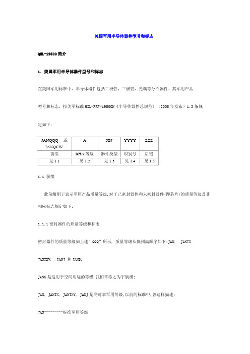
美国军用半导体器件型号和标志QML-19500简介1.美国军用半导体器件型号和标志在美国军用标准中,半导体器件包括二极管,三极管,光藕等分立器件。
其军用产品型号和标志,按美军标准MIL-PRF-19500N《半导体器件总规范》(2005年发布)1.3条规定如下:A XN YYYY ZZZJANQQQ 或JANQCW前缀RHA等级器件类型识别号后缀见1.1见1.2见1.3见1.4.见1.51.1 前缀此前缀用于表示军用产品质量等级.对于已密封器件和未密封器件(即芯片)的质量等级及其相应标志规定如下:1.1.1密封器件的质量等级和标志密封器件的质量等级如上述”QQQ”所示, 质量等级从低到高顺序如下:JAN, JANTX JANTXV, JANJ 和JANS.JANS是适用于空间用途的等级,我们常称之为宇航级;JAN, JANTX, JANTXV, JANJ是高可靠军用等级,以前的标准中,曾这样描述:JAN---------标准军用等级JANTX-----特军级JANTXV---超特军级JANJ--------按标准规定,应在JANS生产线制造,质量等级比JANTXV高.1.1.2未密封器件即芯片的质量等级和标志未密封器件的质量等级如上述”QC”所述,质量等级从低到高顺序如下; JANHCJANKC.JANHC---适用于标准军事用途JANKC---适用于空间(宇航)用途上述”QCW”中的”W”表示此类产品—芯片,必须将适用的等级标志符,标志在包装盒的适当位置上.1.1.3 JAN和J标志按MIL—PRF—19500N 3.10.6.1条规定,当器件打印标志的位置较小时,“JAN”标志可以简化为“J”.这二个标志都是向联邦政府注册的,“JAN”的注册号为:504860;“J”的注册号为:1586261.因此,当器件管壳较小时,军用产品质量等级可以标志如下缩写前缀:质量等级 质量等级缩写JAN------------------- JJANTX----------------- JXJANTXV------------- JVJANJ------------------ JJJANS----------------- JS1.2 辐射加固保证(RHA)等级RHA等级采用一个字母表示,其等级从低到高顺序为:M,D,P,L,R,F,G和H.加固剂量如下: (除非另有规定)等级字母总剂量 Rad(si)中子流量 N/cm2M3×1032×1012D1×1042×1012P3×1042×1012L5×1042×1012R1×1052×1012F3×1052×1012G6×1052×1012H1×1062×10121.3 器件类型半导体器件的标志符用“XN”表示,其中“X”用一个数字表示,它比器件有源电极终端(引出端)数目少一,例如,二极管用“1N”表示,三极管用“2N”表示。
1N4148T(TEMIC Semiconductors)中文数据手册「EasyDatasheet」

初稿
固态器件,INC.
14830山谷规模大道*拉米拉达,钙90638 电话:(562)404-7855 *传真:(562)404-1773
设计师数据表
产品特点:
• 超快速恢复:5纳秒最大 • 超小型表面贴装封装 • 圆形标签安装(方形标签可用) • 密封式 • 平面钝化芯片 • 对于高效率应用
0.8 1.3
VDC
25 500
nA
35
:A
75
2.8
pF
5
nsec
案例外形:
ROUND TAB "SM"
2x C iB
尺寸
DIM MIN.
A
.130"
B
.056"
C
.010"
MAX. .146" .064" .022"
A
数据表#:RC0061A
芯片中文手册,看全文,戳
1N4148SM
初稿
固态器件,INC. 14830山谷规模大道*拉米拉达,钙90638 电话:(562)404-7855 *传真:(562)404-1773
电气特性
符号
最大
UNITS
正向电压降
(TA = 25oC,300 - 500:s脉冲)
IF = 10mA
VF1
IF = 100mA
VF2
正向电压降
(300 - 500:s脉冲)
IF = 10mA, T A = 150oC
VF3
IF = 100mA, T A = -55oC
VF4
反向漏电流
(TA = 25oC, 300 :s 最小脉冲)
英语姓名词典【外研社李慎廉 等编著】 J
英语姓名词典【外研社李慎廉等编著】 J.txt24生活如海,宽容作舟,泛舟于海,方知海之宽阔;生活如山,宽容为径,循径登山,方知山之高大;生活如歌,宽容是曲,和曲而歌,方知歌之动听。
JJabez .[男子名] 杰贝兹。
来源于希伯来语,含义是“悲伤,或顶点”(sorrow,or height) Jack 1.[苏格兰人、英格兰人姓氏] 杰克。
来源于古法语教名及拉丁语Jacobus的法语形式 2.[苏格兰人、英格兰人姓氏] 杰克。
John?? 的昵称,可能借自低地德语或荷兰语的昵称Jankin,Jackin,即Jan+昵称后缀 kin 3.[男子名] 杰克。
John?? 的昵称Jackaman 杰卡曼: Jackman 异体,英格兰人姓氏Jackett [英格兰人姓氏] 杰基特。
Jack?? 的昵称Jacketts 杰基茨:取自父名,源自Jackett `含义“杰基特之了”〔son of Jackett), 英格兰人姓氏Jackie .[男子名] 杰基。
John?? 的昵称Jacklin .[英格兰人姓氏] 杰克林。
Jack?? 的昵称Jackling 杰克林:lack的昵称,英格兰人姓氏Jackman 1.[英格兰人姓氏] 杰克曼。
职业名称,来源于Jack,含义是“杰克之仆”(servant of Jack) 2.[英格兰人姓氏] 杰克曼。
法兰西人姓氏的英语形式Jacks [英格兰人姓氏] 杰克斯。
取自父名,来源于Jack,含义是“杰克之子”(son of Jack) Jackson [英格兰人姓氏] 杰克逊。
取自父名,来源于Jack,含义是“杰克之子”(son of Jack) Jacob .[男子名] [英格兰人姓氏] 雅各布。
通过拉丁语而来源于希伯来语教名,含义是“愿上帝保佑追随者,取代者,或欺骗者”(may God protectfollower,supplanter,or deceiver) 昵称Jake??Jacoba .[女子名] 雅各芭。
LL4148数据手册_引脚图_参数
3. TAPING SPECIFICATION & PACKAGING
3
4. MAXIMUM RATINGS (TA=25oC)
Version # Revision# Revision# Revision#
91002 91002A 91002B 91002C
Issue date:
Issue Date: Issue Date Issue Date
Jan.1,1991 Mar.15,2012 Mar. 20,2012 Mar. 29, 2012
G.W.
7. PACKING SPEC
7
8. THE RECOMMENDATION FOR REFLOW SOLDERING CONDITION
9. DATABOOK REFERENCE
The following data references are available for this device: 1. Good-Ark Databook 2. Applications Notes 3. Internet homepage
121-14-2 84-69-5 7758-97-6 12656-85-8
204-450-0 201-553-2 231-846-0 235-759-9
<1000PPM <1000PPM <1000PPM
<1000PPM
29
Lead sulfochromate yellow(C.I.Pigment
JANTXV1N5524中文资料
MOUNTING SURFACE SELECTION: The Axial Coefficient of Expansion (COE) Of this Device is Approximately +6PPM/°C. The COE of the Mounting Surface System Should Be Selected To Provide A Suitable Match With This Device.
ZENER IMPEDANCE VS. OPERATING CURRENT
144
mA
µ Adc
5.0 3.0 1.0 3.0 2.0 2.0 2.0 1.0 1.0 0.5 0.5 0.1 0.05 0.05 0.05 0.01 0.01 0.01 0.01 0.01 0.01 0.01 0.01 0.01 0.01 0.01 0.01 0.01 0.01
mA
mA
CDLL5518B CDLL5519B CDLL5520B CDLL5521B CDLL5522B CDLL5523B CDLL5524B CDLL5525B CDLL5526B CDLL5527B CDLL5528B CDLL5529B CDLL5530B CDLL5531B CDLL5532B CDLL5533B CDLL5534B CDLL5535B CDLL5536B CDLL5537B CDLL5538B CDLL5539B CDLL5540B CDLL5541B CDLL5542B CDLL5543B CDLL5544B CDLL5545B CDLL5546B
0.90 0.90 0.85 0.75 0.60 0.65 0.30 0.20 0.10 0.05 0.05 0.05 0.10 0.20 0.20 0.20 0.20 0.20 0.20 0.20 0.20 0.20 0.20 0.25 0.30 0.35 0.40 0.45 0.50
1N4148(Won-Top Electronics)中文数据手册「EasyDatasheet」

to part number above. For example, 1N4148-TB-LF.
数量
(PCS) 25,000
100,000
120,000
约.总重量 (KG) 8.5
15.7
13.8
1N4148
3 of 4
©2006韩元鼎好电子
芯片中文手册,看全文,戳
订购信息
产品编号
1N4148-T3 1N4148-TB 1N4148
封装类型
DO-35 DO-35 DO-35
WARNING: DO NOT USE IN LIFE SUPPORT EQUIPMENT. WTE power semiconductor productsare not authorized for use ascritical componentsin life support devicesor systemswithout the expresswritten approval.
新 增 "-LF"后 缀 型 号 ,见 第 4页
1N4148 Pb
快速开关二极管
A
B
A
C D
DO-35
Dim
Min
Max
A
25.40
—
B
—
4.00
C
—
0.60
D
—
2.00
在毫米所有尺寸
1N4754中文资料
at IZK mA 1.0 1.0 1.0 1.0 1.0 1.0 1.0 1.0 1.0 0.5 0.5 0.5 0.25 0.25 0.25 0.25 0.25 0.25 0.25 0.25 0.25 0.25 0.25 0.25 0.25 0.25 0.25 0.25 0.25 0.25 0.25 0.25 0.25 0.25 0.25 0.25 0.25
Test current
Maximum Zener impedance(1)
Maximum reverse leakage current at VR V 1 1 1 1 1 1 2 3 4 5 6 7 7.6 8.4 9.1 9.9 11.4 12.2 13.7 15.2 16.7 18.2 20.6 22.8 25.1 27.4 29.7 32.7 35.8 38.8 42.6 47.1 51.7 56.0 62.2 69.2 76.0
max. .161 (4.1) min. 1.102 (28.0)
max. ∅ 0.102 (2.6)
Cathode Mark
min. 1.102 (28.0)
max. ∅ 0.034 (0.86)
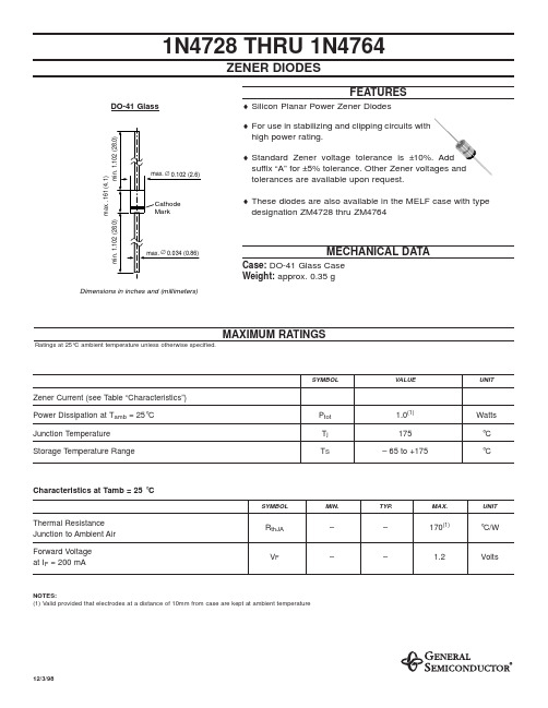
MECHANICAL DATA
Case: DO-41 Glass Case Weight: approx. 0.35 g
–
1.2
Volts
NOTES: (1) Valid provided that electrodes at a distance of 10mm from case are kept at ambient temperature
12/3/98
元器件交易网
1N4728 THRU 1N4764
1N4123C中文资料
µA
10 10 1.0 1.0 1.0 1.0 .05 .05 .05 .05 .05 .05 .05 .05 .05 .01 .01 .01 .01 .01 .01 .01 .01 .01 .01 .01 .01 .01 .01 .01 .01 .01 .01 .01 .01 .01 .01
VOLTS 5.17 5.70 6.24 6.61 6.92 7.60 8.44 9.12 9.87 10.65 11.40 12.15 12.92 13.67 14.44 15.20 16.72 18.25 19.00 20.46 21.28 22.80 25.08 27.38 29.65 32.65 35.75 38.76 42.60 45.60 47.10 51.68 57.00 62.32 66.12 69.16 76.00
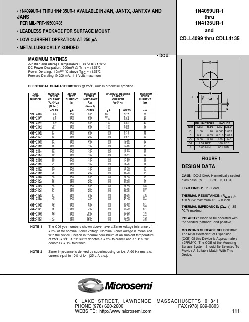
FIGURE 1
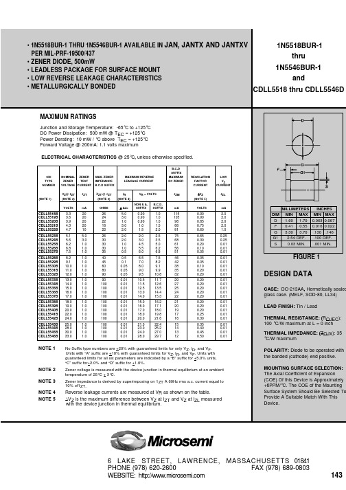
DESIGN DATA
CASE: DO-213AA, Hermetically sealed glass case. (MELF, SOD-80, LL34) LEAD FINISH: Tin / Lead THERMAL RESISTANCE: (ROJEC): 100 °C/W maximum at L = 0 inch THERMAL IMPEDANCE: (ZOJX): 35 °C/W maximum POLARITY: Diode to be operated with the banded (cathode) end positive. MOUNTING SURFACE SELECTION: The Axial Coefficient of Expansion (COE) Of this Device is Approximately +6PPM/°C. The COE of the Mounting Surface System Should Be Selected To Provide A Suitable Match With This Device.
1N4148T中文资料

Silicon Epitaxial Planar DiodesMax Unit1001000m A ) 1 N 4448TELEFUNKEN Semiconductors4 (4)Ozone Depleting Substances Policy StatementIt is the policy of TEMIC TELEFUNKEN microelectronic GmbH to 1.Meet all present and future national and international statutory requirements.2.Regularly and continuously improve the performance of our products, processes, distribution and operating systems with respect to their impact on the health and safety of our employees and the public, as well as their impact on the environment.It is particular concern to control or eliminate releases of those substances into the atmosphere which are known as ozone depleting substances (ODSs).The Montreal Protocol (1987) and its London Amendments (1990) intend to severely restrict the use of ODSs and forbid their use within the next ten years. Various national and international initiatives are pressing for an earlier ban on these substances.TEMIC TELEFUNKEN microelectronic GmbH semiconductor division has been able to use its policy of continuous improvements to eliminate the use of ODSs listed in the following documents.1.Annex A, B and list of transitional substances of the Montreal Protocol and the London Amendments respectively2.Class I and II ozone depleting substances in the Clean Air Act Amendments of 1990 by the Environmental Protection Agency (EPA) in the USA3.Council Decision 88/540/EEC and 91/690/EEC Annex A, B and C (transitional substances) respectively.TEMIC can certify that our semiconductors are not manufactured with ozone depleting substances and do not contain such substances.We reserve the right to make changes to improve technical design and may do so without further notice .Parameters can vary in different applications. All operating parameters must be validated for each customer application by the customer. Should the buyer use TEMIC products for any unintended or unauthorized application, the buyer shall indemnify TEMIC against all claims, costs, damages, and expenses, arising out of,directly or indirectly, any claim of personal damage, injury or death associated with such unintended orunauthorized use.TEMIC TELEFUNKEN microelectronic GmbH, P.O.B. 3535, D-74025 Heilbronn, GermanyTelephone: 49 (0)7131 67 2831, Fax number: 49 (0)7131 67 2423。
1N4148WS

1N4148WS / 1N4448WS / 1N914BWS — Small Signal Diodes1N4148WS / 1N4448WS / 1N914BWS — Small Signal Diodes1N4148WS / 1N4448WS / 1N914BWS Small Signal Diodes1N4148WS / 1N4448WS / 1N914BWSRev. I31TRADEMARKSThe following are registered and unregistered trademarks and service marks Fairchild Semiconductor owns or is authorized to use andis not intended to be an exhaustive list of all such trademarks.DISCLAIMERFAIRCHILD SEMICONDUCTOR RESERVES THE RIGHT TO MAKE CHANGES WITHOUT FURTHER NOTICE TO ANY PRODUCTS HEREIN TO IMPROVE RELIABILITY, FUNCTION, OR DESIGN. FAIRCHILD DOES NOT ASSUME ANY LIABILITY ARISING OUT OF THE APPLICATION OR USE OF ANY PRODUCT OR CIRCUIT DESCRIBED HEREIN; NEITHER DOES IT CONVEY ANY LICENSE UNDER ITS PATENT RIGHTS, NOR THE RIGHTS OF OTHERS. THESE SPECIFICATIONS DO NOT EXPAND THE TERMS OF FAIRCHILD’S WORLDWIDE TERMS AND CONDITIONS, SPECIFICALLY THE WARRANTY THEREIN, WHICH COVERS THESE PRODUCTS.LIFE SUPPORT POLICYFAIRCHILD’S PRODUCTS ARE NOT AUTHORIZED FOR USE AS CRITICAL COMPONENTS IN LIFE SUPPORT DEVICES OR SYSTEMS WITHOUT THE EXPRESS WRITTEN APPROVAL OF FAIRCHILD SEMICONDUCTOR CORPORATION.As used herein:1. Life support devices or systems are devices or systemswhich, (a) are intended for surgical implant into the body, or (b) support or sustain life, and (c) whose failure to perform when properly used in accordance with instructions for use provided in the labeling, can be reasonably expected to result in significant injury to the user.2.A critical component is any component of a life support device or system whose failure to perform can be reasonably expected to cause the failure of the life support device or system, or to affect its safety or effectiveness.PRODUCT STATUS DEFINITIONS Definition of Terms ACEx ®Build it Now™CorePLUS™CROSSVOLT ™CTL™Current Transfer Logic™EcoSPARK ®Fairchild ®Fairchild Semiconductor ®FACT Quiet Series™FACT ®FAST ®FastvCore™FPS™FRFET ®Global Power Resource SMGreen FPS™Green FPS™ e-Series™GTO™i-Lo ™IntelliMAX™ISOPLANAR™MegaBuck™MICROCOUPLER™MicroFET™MicroPak™MillerDrive™Motion-SPM™OPTOLOGIC ®OPTOPLANAR ®®PDP-SPM™Power220®Power247®POWEREDGE ®Power-SPM™PowerTrench ®Programmable Active Droop™QFET ®QS™QT Optoelectronics™Quiet Series™RapidConfigure™SMART START™SPM ®STEALTH™SuperFET™SuperSOT™-3SuperSOT™-6SuperSOT™-8SyncFET™The Power Franchise ®TinyBoost™TinyBuck™TinyLogic ®TINYOPTO™TinyPower™TinyPWM™TinyWire™µSerDes™UHC ®UniFET™VCX™Datasheet IdentificationProduct StatusDefinitionAdvance Information Formative or In DesignThis datasheet contains the design specifications for product development. Specifications may change in any manner without notice.Preliminary First ProductionThis datasheet contains preliminary data; supplementary data will be pub-lished at a later date. Fairchild Semiconductor reserves the right to make changes at any time without notice to improve design.No Identification Needed Full ProductionThis datasheet contains final specifications. Fairchild Semiconductor reserves the right to make changes at any time without notice to improve design. Obsolete Not In ProductionThis datasheet contains specifications on a product that has been discontin-ued by Fairchild semiconductor. The datasheet is printed for reference infor-mation only.。
1884144资料
Address
PHOENIX CONTACT GmbH & Co. KG Flachsmarktstr. 8 32825 Blomberg,Germany Phone +49 5235 3 00 Fax +49 5235 3 41200 http://www.phoenixcontact.de
PHOENIX CONTACT GmbH & Co. KG http://www.phoenixcontact.de
Page 2 / 4 Mar 6, 2008
元器件交易网
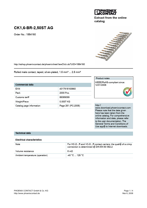
CK1,6-BR-2,50ST AG Order No.: 1884160
http://eshop.phoenixcontact.de/phoenix/treeViewClick.do?UID=1884160
2 2
Approval logo
requested approbations Certification Accessories Item General 1884869 Tools 1676734 1884843 CK1,6/2,5-MWZ CRIMPFOX-1,6-ER-1,50-AT Assembly tool, for CK 1.6... crimp contacts for small conductor cross sections Crimping pliers for rolled contacts CK 1.6-ER... and ...-BR..., 0.5 1.5 mm² VC-EW 1,6 Contact removal tool, for turned and rolled CK- 1.6-... contacts Designation Description GOST
414J;中文规格书,Datasheet资料
/
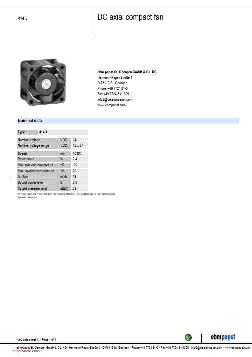
414 J
DC axial compact fan
Product drawing
Web data sheet XI · Page 3 of 4 ebm-papst St. Georgen GmbH & Co. KG · Hermann-Papst-Straße 1 · D-78112 St. Georgen · Phone +49 7724 81-0 · Fax +49 7724 81-1309 · info2@ ·
/
414 J
DC axial compact fan
Charts: Air flow
(in H ² O) 0,1 0,2 0,3 0,6 0,5
150 125 100 75 50 25
D pf S
Pa
0
2
4
6
8
10
12
CFM m³/h
VS
•
5
10
15
20
Web data sheet XI · Page 4 of 4 ebm-papst St. Georgen GmbH & Co. KG · Hermann-Papst-Straße 1 · D-78112 St. Georgen · Phone +49 7724 81-0 · Fax +49 7724 81-1309 · info2@ ·
414 J
DC axial compact ቤተ መጻሕፍቲ ባይዱan
ebm-papst St. Georgen GmbH & Co. KG Hermann-Papst-Straße 1 D-78112 St. Georgen Phone +49 7724 81-0 Fax +49 7724 81-1309 info2@
- 1、下载文档前请自行甄别文档内容的完整性,平台不提供额外的编辑、内容补充、找答案等附加服务。
- 2、"仅部分预览"的文档,不可在线预览部分如存在完整性等问题,可反馈申请退款(可完整预览的文档不适用该条件!)。
- 3、如文档侵犯您的权益,请联系客服反馈,我们会尽快为您处理(人工客服工作时间:9:00-18:30)。
MIL-PRF-19500/116L 8 June 2001SUPERSEDINGMIL-PRF-19500/116K 28 February 1997PERFORMANCE SPECIFICATIONSEMICONDUCTOR DEVICE, DIODE, SILICON, SWITCHINGTYPES 1N914, 1N914UR, 1N4148-1, 1N4148UR-1, 1N4148UB, 1N4148UB2, 1N4148UB2R, 1N4148UBCA,1N4148UBCC, 1N4148UBCD, 1N4531, AND 1N4531UR, JAN, JANTX, JANTXV, JANHC, AND JANKCJANS1N4148-1 (see 6.4). Device types 1N914and 1N4531 are inactive for new design.This specification is approved for use by all Departments and Agencies of the Department of Defense.1. SCOPE1.1 Scope. This specification covers the performance requirements for silicon, diffused, switching diodes. Three levels of product assurance are provided for each device type as specified in MIL-PRF-19500. Two levels of product assurance are provided for each unencapsulated device.1.2 Physical dimensions. See figures 1 (similar to DO-35), 2, 3, 4, and 5.1.3 Maximum ratings.TypeV (BR)V RWMI oT A = 25q CI FSM t p =1/120 s T STGT opZ 6JXR 6JLR 6JCV dcV (pk)mA A (pk)q C q C q C/W q C/W q C/W 1N914, UR 1007575 (1)1-65 to +200-65 to +17570N/A 1N4531, UR 10075125 (2)1-65 to +200-65 to +17570250N/A 1N4148-1, UR-110075200 (3)2-65 to +200-65 to +20070(leaded)N/A 1N4148UB,1N4148UB2,1N4148UB2R,1N4148UBCA,1N4148UBCC ,1N4148UBCD,10075200 (3)2-65 to +200-65 to +20070100(UR)150(1) Derate at 0.5 mA/G C above T A = 25G C.(2) Derate at 0.83 mA/G C above T A = 25G C.(3) Derate at 1.14 mA/G C above T A = 25G C.Beneficial comments (recommendations, additions, deletions) and any pertinent data which may be of use in improving this document should be addressed to: Defense Supply Center, Columbus, ATTN: DSCC-VAC,P.O. Box 3990, Columbus, OH 43216-5000, by using the Standardization Document Improvement Proposal (DD Form 1426) appearing at the end of this document or by letter.AMSC N/AFSC 5961DISTRIBUTION STATEMENT A. Approved for public release; distribution is unlimited.INCH POUND The documentation and process conversion measures necessary to comply with thisrevision shall be completed by 8 September 2001.1.4 Primary electrical characteristics at T A = +25G C, unless otherwise indicated.Type (1)V F1V F2I R1 atV R= 20 V dcI R2 atV R = 75 V dc1N9141N4148-1 1N4531I F mA dc101010V dc0.80.80.8I F mA dc50100100V dc1.21.21.2nA dc2525252A dc0.50.50.5Type (1)I R3 atV R = 20 V dcT A = 150G CI R4 atV R = 75 V dcT A = 150G Ct fr atV fr = 5.0 V dc (pk) andI F = 50 mA dct rr1N9141N4148-1 1N45312A dc3535352A dc757575ns202020ns555(1) Electrical characteristics for surface mount devices are equivalent to the corresponding non-surface mountdevices unless otherwise noted.2. APPLICABLE DOCUMENTS2.1 General. The documents listed in this section are specified in sections 3 and 4 of this specification. This section does not include documents cited in other sections of this specification or recommended for additional information or as examples. While every effort has been made to ensure the completeness of this list, document users are cautioned that they must meet all specified requirements documents cited in sections 3 and 4 of this specification, whether or not they are listed.2.2 Government documents.2.2.1 Specifications, standards, and handbooks. The following specifications, standards, and handbooks form a part of this document to the extent specified herein. Unless otherwise specified, the issues of these documents are those listed in the issue of the Department of Defense Index of Specifications and Standards (DoDISS) and supplement thereto, cited in the solicitation (see 6.2).SPECIFICATIONDEPARTMENT OF DEFENSEMIL-PRF-19500-Semiconductor Devices, General Specification for.STANDARDDEPARTMENT OF DEFENSEMIL-STD-750-Test Methods for Semiconductor Devices.(Unless otherwise indicated, copies of the above specifications, standards, and handbooks are available from the Document Automation and Production Services (DAPS), Building 4D (DPM-DODSSP), 700 Robbins Avenue, Philadelphia, PA 19111-5094.)2Types Dimensions Notes1, 2Ltr Inches MillimetersMin Max Min Max1N4148-1BL.140.180 3.56 4.5731N914BD.056.075 1.42 1.904LL 1.000 1.50025.4038.10LD.018.0220.460.5651N4531BL.080.120 2.03 3.05BD.050.075 1.27 1.904LL 1.000 1.50025.4038.10LD.018.0220.460.565NOTES:1. Dimensions are in inches.2. Metric equivalents are given for general information only.3. Ferrule is optional on types 1N4148-1 and 1N4531 for dimension BL.4. The minimum dimension of BD shall apply over at least .075 (1.90 mm) of dimension BL.5. The specified lead diameter applies in the zone between .050 (1.27 mm) for 1N914, and 1N4148-1,and .010 (0.25mm) for 1N4531 from the diode body to the end of the lead. Outside of this zone the lead shall not exceed BD.FIGURE 1. Semiconductor device, diode, types 1N914, 1N4148-1, and 1N4531.3Symbol DimensionsInches MillimetersMin Max Min MaxBD.063.067 1.60 1.70ECT.016.0220.410.55BL.130.146 3.30 3.70S.001 min0.03 minNOTES:1. Dimensions are in inches.2. Metric equivalents are given for general information only.FIGURE 2. Physical dimensions 1N914UR, 1N4148UR-1, AND 1N4531UR.41321N4148UBCA11N4148UB231131N4148UBD31N4148UBCC 22DimensionsSymbol Inches Millimeters Symbol Inches Millimeters Min Max Min Max Min Max Min Max A0.0460.0560.97 1.42D10.0710.078 1.81 2.01 A10.0170.0230.430.58D2B10.0160.0240.410.61D3B20.0160.0240.410.61E0.1150.125 2.82 3.18 B30.0160.0240.410.61E3- - -- - -D0.0850.105 2.41 2.67L10.0220.0380.560.96L20.0240.0360.610.81 NOTES:1. Dimensions are in inches.2. Metric equivalents are given for general information only.3. Ceramic package only.FIGURE 3. Physical dimensions, surface mount (UB versions).5DimensionsSymbol Inches Millimeters NoteMin Max Min MaxA0.0460.0560.97 1.42A10.0170.0350.430.89B10.0160.0240.410.61TypB20.0160.0240.410.61TypR20.0120.3TypD0.0850.108 2.41 2.74D10.0710.078 1.81 2.01D20.0350.0390.890.99D30.0850.108 2.41 2.74E0.1150.128 2.82 3.25E3- - -0.128- - - 3.25L10.0220.0380.560.96R30.008R0.2RR10.022R0.55RNOTES:1. Dimensions are in inches.2. Metric equivalents are given for general information only.FIGURE 4. Physical dimensions, surface mount (2 pin UB version).67DimensionsLtrInchesMillimeters MinMax MinMax A .0059.0061.150.155B.0130.0170.330.430NOTES:1.Dimensions are in inches.2.Metric equivalents are given for general information only.3.Element evaluation accomplished utilizing TO-5 package.4.The physical characteristics of the die are:Metallization:Top (anode): Al. Back (cathode): Au.Al thickness: 25,000 Å minimum. Gold thickness: 4,000 Å minimum.Chip thickness: .010 inches (.25 mm) H .002 inches (.05 mm).FIGURE 5. Physical dimensions, JANHCA and JANKCA die.2.3 Order of precedence. In the event of a conflict between the text of this document and the references cited herein the text of this document takes precedence. Nothing in this document, however, supersedes applicable laws and regulations unless a specific exemption has been obtained.3. REQUIREMENTS3.1 General. The requirements for acquiring the product described herein shall consist of this document andMIL-PRF-19500.3.2 Qualification. Devices furnished under this specification shall be products that are manufactured by a manufacturer authorized by the qualifying activity for listing on the applicable qualified manufacturer's list (QML) before contract award (see4.2 and 6.3).3.3 Abbreviations, symbols, and definitions. Abbreviations, symbols, and definitions used herein shall be as specified in MIL-PRF-19500 and as follows.VForward recovery voltage. Specified maximum forward voltage used to determine forward recovery frtime.LS Lead spacing distance between device body and electrical/mechanical contact on lead.UB Hermetic unleaded 3 terminal (LCC, Leadless Chip Carrier) package type.UR Unleaded round package type designation.3.4 Interface and physical dimensions. Interface and physical dimensions shall be as specified inMIL-PRF-19500, and on figures 1, 2, 3, 4, and 5 herein.3.4.1 Lead finish. Lead finish shall be solderable in accordance with MIL-PRF-19500, MIL-STD-750, and herein. Where a choice of lead finish is desired, it shall be specified in the acquisition document (see 6.2).3.4.2 Diode construction. All devices (except UB version) shall be metallurgically bonded double plug construction in accordance with the requirements of category I, II, or III (see MIL-PRF-19500). The UB package shall be wire bonded, eutectically mounted devices.3.5 Electrical performance characteristics. Unless otherwise specified herein, the electrical performance characteristics are as specified in 1.3, 1.4, and table I.3.6 Electrical test requirements. The electrical test requirements shall be the subgroups specified in4.4.2 and4.4.3 herein.3.7 Marking. Marking shall be in accordance with MIL-PRF-19500. At the option of the manufacturer, marking may be omitted from the body, but shall be retained on the initial container.3.7.1 UR devices. "UR" devices shall be marked with a cathode band only. Initial container package marking shall be in accordance with MIL-PRF-19500.3.7.2 UB devices. The part number may be reduced to J4148, JX4148, or JV4148. Manufacturers identification and date code shall be marked on the devices.3.7.3 UBR devices. The part number may be reduced to J4148, JX4148, or JV4148. Manufacturers identification and date code shall be marked on the devices.3.8 Polarity. The polarity shall be indicated with a contrasting color band to denote the cathode end. No color coding will be permitted. UB packages do not require polarity marking.3.9 Workmanship. Semiconductor devices shall be processed in such a manner as to be uniform in quality and shall be free from other defects that will affect life, serviceability, or appearance.894. VERIFICATION4.1 Classification of inspections. The inspection requirements specified herein are classified as follows:a. Qualification inspection (see 4.2).b. Screening (see 4.3).c. Conformance inspection (see 4.4).4.2 Qualification inspection. Qualification inspection shall be in accordance with MIL-PRF-19500 and as specified herein.4.2.1 Group E inspection. Group E inspection shall be in accordance with MIL-PRF-19500 and table II herein.4.3 Screening (JAN, JANTX, and JANTXV levels only). Screening shall be in accordance with table IV ofMIL-PRF-19500 and as specified herein. The following measurements shall be made in accordance with table I herein. Devices that exceed the limits of table I herein shall not be acceptable.Screen (see table IV Measurementof MIL-PRF-19500)JAN levelJANTX and JANTXV levels 3a Temperature cycling in accordance with MIL-PRF-19500 TX level.Temperature cycling3c (1)Thermal impedance (see 4.5.5)Thermal impedance (see 4.5.5)9Not applicable Not applicable10 (2)Not applicable Method 1038, condition A, t = 48 hours 11Not applicable I R1 and V F112Not applicable See 4.3.1, t = 48 hours13Not applicable(3) Subgroup 2 of table I herein;'I R1 = 100 percent of initial reading or 15 nA, whichever is greater; 'V F1 = 25 mV dc.PDA = 10 percent(1)Thermal impedance shall be performed any time after sealing provided temperature cycling is performed inaccordance with MIL-PRF-19500, screen 3 prior to this thermal test.(2)Test within 24 hours after removal from test.(3)When thermal impedance is performed prior to screen 13, it is not required to be repeated in screen 13.4.3.1 Burn-in test conditions. Burn-in conditions are as follows:Type T A +30q C r 5q C V RWM = 75 V (pk)f = 50 - 60 Hz T A = +30q C r 5q C1N914, 1N914UR I O = 75 mA I F =150 mA min 1N4531, 1N4531URI O = 125 mA I F = 175 mA min 1N4148-1, 1N4148UR-1, 1N4148UB,1N4148UB2, 1N4148UBR2I O = 200 mAI F = 200 mA min104.4 Conformance inspection. Conformance inspection shall be in accordance with MIL-PRF-19500 and as specified herein.4.4.1 Group A inspection. Group A inspection shall be conducted in accordance with MIL-PRF-19500 and table I herein. Electrical measurements (end-points) shall be in accordance with Table I, group A, subgroup 2 herein.4.4.2 Group B inspection. Group B inspection shall be conducted in accordance with the conditions specified for subgroup testing in table VIb (JANTX and JANTXV) of MIL-PRF-19500 and as specified herein. Electricalmeasurements (end-points) shall be in accordance with Table I, group A, subgroup 2 herein except for the thermal impedance test.4.4.2.1 Group B inspection, table VIb (JANTX, JANTXV) of MIL-PRF-19500.Subgroup Method ConditionsB22005I F = 100 mA, axial tensile stress = 8 lbs, T A = +150G C; (not applicable to UR or UB package). (This test shall be performed as the first test of subgroup 2).B3 1027T A = +30G C H 5G C, V RWM = 75 V(pk), f = 50-60 Hz (see 4.5.1); 1N914: I O = 5 mA,1N4531: I O = 125 mA, 1N4148-1: I O = 200 mA.B4 2075See 4.5.4 herein.B53101R 6JL = 250G C/W, .375 inch (9.52 mm) lead length (non-surface mount). or 4081R 6JL 100G C/W (UR), R 6JC = 150G C/W (UB).4.4.3 Group C inspection. Group C inspection shall be conducted in accordance with the conditions specified for subgroup testing in table VII of MIL-PRF-19500, and as follows. Electrical measurements (end-points) shall be in accordance with Table I, group A, subgroup 2 herein except for the thermal impedance test.Subgroup Method Conditions C2 1056100 cycles.C22036Tension: Test condition A, t = 15 seconds, weight = 10 pounds. Lead fatigue:Test condition E. Terminal strength and lead fatigue not applicable to UB or UR devices.C6 1026T A = +30G C H 5G C, V RWM = 75 V(pk), f = 50-60 Hz (see 4.5.1), for:1N914I O = 75 mA.1N4531I O = 125 mA.1N4148-1I O = 200 mA.4.5 Methods of inspection. Methods of inspection shall be as specified in the appropriate tables and as follows.4.5.1 Pulse measurements. Conditions for pulse measurements shall be specified in section 4 of MIL-STD-750.4.5.2 Life tests. AC tests shall be conducted with a half-sine wave of the peak voltage specified herein impressed across the diode in the reverse direction, followed by a half-sine waveform of the average rectified current specified herein. The forward conduction angle of the rectified current shall be not greater than 180 degree nor less than 150 degree.114.5.3 Forward recovery voltage and time. Forward recovery time shall be measured as the time interval between zero time and the point where the pulse has decreased to 110 percent of the steady-state value of V F when I F = 50 mA dc. The maximum rise time of the response detector shall be 1 ns.4.5.4 Decap internal visual scribe and break (not applicable to UB package). Scratch glass at cavity area with diamond scribe. Carefully snap open. Using 30X magnification examine the area where die was in contact with the plugs, verify footprint for minimum of 15 percent metallurgical bonding area. In addition, a cross sectional view may be used to verify consistency of construction. A cross sectional view shall be used exclusively for construction verification and shall not be used to verify bond integrity. The UB package shall employ the manufacturers’ normal delidding procedures.4.5.5 Thermal impedance (Z 6JX measurements). Thermal impedance measurements shall be in accordance method 3101 MIL-STD-750, and as follows.a.I H = 300 mA to 500 mA.b.t H = 10 ms.c.I M = 1 mA to 10 mA.d.t MD = 70 2s maximum.The maximum limit for Z 6JX under these test conditions is Z6JX= 70G C/W.4.5.5.1 For initial qualification or requalification. Read and record data (Z 6JX ) shall be supplied to the qualifying activity on one lot (random sample of 500 devices minimum) prior to shipment. Twenty two samples shall be serialized and provided to the qualifying activity for test correlation.4.5.6 Thermal resistance. Thermal resistance measurement shall be in accordance with method 3101MIL-STD-750, or method 4081 of MIL-STD-750. Forced moving air or draft shall not be permitted across the device during test. The maximum limit for R 6JL under these test conditions shall be as shown in group B of 4.4.2.1 and group E of table II. The following conditions shall apply when using method 3101:a.I H - - - - - - - - - - - - - - - - - - - - - - - - - - - 75 mA to 300 mA.b.t H - - - - - - - - - - - - - - - - - - - - - - - - - - - 25 seconds minimum.c.I M - - - - - - - - - - - - - - - - - - - - - - - - - - - 1 mA to 10 mA.d.t MD - - - - - - - - - - - - - - - - - - - - - - - - - - 70 2s maximum.4.5.6.1 Lead spacing for leaded devices:LS = Lead spacing = .375 inch (9.53 mm) as defined on figure 6.FIGURE 6. Mounting conditions.4.5.6.2 Temperature reference (T r) unleaded devices (UB, UR suffix). The temperature reference point shall be the hottest portion of the external surface. As an alternate, the temperature of a stream of liquid used to cool the device during the test may be used as the temperature reference point.12TABLE I. Group A inspection.MIL-STD-750LimitsInspection 1/Method Conditions Symbol Min Max Unit Subgroup 1Visual and mechanicalinspection2071Subgroup 2Thermal impedance3101See 4.5.5Z6JX70q C/WForward voltage4011IF = 10 mA dc V F10.8V dcBreakdown voltage4021IR = 100 P A dc V BR1100V dcReverse current 1N9141N45311N4148-14016DC methodV R = 20 V dcI R1252525nA dcnA dcnA dcReverse current4016DC methodV R = 75 V dcI R2500nA dcForward voltage4011I F = 50 mA dcI F = 100 mA dcI F = 100 mA dc V F21.21.21.2V dcV dcV dcSubgroup 3High temperatureoperation:T A = +150q CReverse current 1N9141N45311N4148-14016DC methodV R = 20 V dcI R335P A dcReverse current 1N9141N45311N4148-14016DC methodV R = 75 V dcI R4757575P A dcP A dcP A dcForward voltage 1N9141N45311N4148-14011IF = 10 mA dc V F30.80.80.8V dcV dcV dcSee footnote at end of table.13TABLE I. Group A inspection - Continued.MIL-STD-750LimitsInspection 1/Method Conditions Symbol Min Max Unit Subgroup 3 -ContinuedLow temperatureoperation:T A = -55q CForward voltage4011V F41N9141N4531 1N4148-1I F = 50 mA dcI F = 100 mA dcI F = 100 mA dc1.31.31.3V dcV dcV dcSubgroup 4Junction capacitance4001VR = 0 V dc, f = 1 MHz,V sig = 50 mV p-p maximumC11N9141N4531 1N4148-14.04.04.0pFpFpFJunction capacitance4001VR = 1.5 V dc, f = 1 MHz,V sig = 50 mV p-p maximumC2 2.8pFReverse recovery time4031Condition AC > 1 nF, I F = I R = 10 mA dc, R L = 100:r5%I R(REC) = 1.0 mA dc, R t 1000:.t rr5ns1N9141N45311N4148-1Subgroup 5Not applicableSee footnote at end of table.14TABLE I. Group A inspection - Continued.MIL-STD-750LimitsInspection 1/Method Conditions Symbol Min Max Unit Subgroup 6Surge current4066Condition A (sine wave)i f(surge) = 1 A (pk) for 1N914 and 1N4531i f(surge) = 2 A (pk) for 1N4148-1, UR and1N4148UB, I O = maximum rateddc current = 0V RM = 010 surges, 8.3 ms width each,one surge per minute, T A = +25q CorCondition B (square wave)I F(surge) = 0.704 A (pk) for1N914, 1N4531, and 1N4148UBI F(surge) = 1.41 A (pk) for1N4148-1t p = 8.3 msn = 10d.f. = 0.0055%T A = 25q CElectrical measurements See table I, subgroup 2Subgroup 7Forward recovery voltage and time 4026IF = 50 mA dc(see 4.5.2)V frt fr5.020V (pk)ns1/ For sampling plan, see MIL-PRF-19500.15TABLE II. Group E inspection (all quality levels) for qualification only.MIL-STD-750Inspection 1/Method Conditions Sampling plan Subgroup 145 devices c = 0 Thermal shockglass strain)10561,000 cyclesElectrical measurements See table I, subgroup 2Subgroup 245 devices c = 0Intermittentoperating lifeElectrical measurements 103710,000 cyclesSee table I, subgroup 2Subgroup 3Not applicableSubgroup 422 devices c = 0Thermal resistance surface mount 3101or4081R"JEC = 100q C/W (maximum) at zero lead length(for UR),R"JEC= 150q C/W (maximum) for UB.(see 4.5.6), +25q C d T R d +35q CThermal resistance leaded devices 3101or4081R"JEC = 250q C/W (maximum)+25q C d T R d +35q C, (see 4.5.6)t H t 25s in still air.Subgroup 522 devices c = 0 Monitored missiontemperature cycling1055Not required for UB suffix devices.Electrical measurements See table I, subgroup 2165. PACKAGING5.1 Packaging. For acquisition purposes, the packaging requirements shall be as specified in the contract or order (see6.2). When actual packaging of materiel is to be performed by DoD personnel, these personnel need to contact the responsible packaging activity to ascertain requisite packaging requirements. Packaging requirements are maintained by the Inventory Control Point’s packaging activity within the Military Department or Defense Agency, or within the Military Department’s System Command. Packaging data retrieval is available from the managing Military Department’s or Defense Agency's automated packaging files, CD-ROM products, or by contacting the responsible packaging activity.6. NOTES(This section contains information of a general or explanatory nature that may be helpful, but is not mandatory.) 6.1 Intended use. The notes specified in MIL-PRF-19500 are applicable to this specification.6.2 Acquisition requirements. Acquisition documents must specify the following:a.Title, number, and date of this specification.b.Issue of DoDISS to be cited in the solicitation and, if required, the specific issue of individual documentsreferenced (see 2.2.1).c.Packaging requirements (see 5.1).d.Lead finish (see 3.4.1).e.Type designation and product assurance level.6.3 Qualification. With respect to products requiring qualification, awards will be made only for products which are, at the time of award of contract, qualified for inclusion in Qualified Manufacturers' List (QML) whether or not such products have actually been so listed by that date. The attention of the contractors is called to these requirements, and manufacturers are urged to arrange to have the products that they propose to offer to the Federal Government tested for qualification in order that they may be eligible to be awarded contracts or orders for the products covered by this specification. Information pertaining to qualification of products may be obtained from Defense Supply Center, Columbus, ATTN: DSCC/VQE, P.O. Box 3990, Columbus, OH 43216-5000.6.4 Cross reference substitution information. The JANS version of 1N6638, 1N6642, or 1N6643(MIL-S-19500/578) is preferred in lieu of the JANS1N4148-1. The JANS 1N6638 or 1N6642 is substitutable for the JANS 1N4148-1 and shall be used in lieu of the JANS1N4148-1. A PIN for PIN replacement table follows, and these devices are directly interchangeable.JANS Non-preferredPINJANS supersededPIN1N4148-11N66381N6642176.5 Suppliers of JANHC and JANKC die. The qualified JANHC and JANKC suppliers with the applicable letter version (example JANHCA1N4148) will be identified on the QPL.JANC ordering informationPIN Manufacturer558011N4148-1 1N4148-1JANHCA1N4148 JANKCA1N41486.6 Changes from previous issue. Marginal notations are not used in this revision to identify changes with respect to the previous issue due to the extent of the changes.Custodians:Preparing activity Army - CR DLA - CCNavy - NWAir Force - 11DLA - CC(Project 5961-2422) Review activities:Army - AR, MI, SMNavy - AS, CG, MCAir Force - 19, 9918STANDARDIZATION DOCUMENT IMPROVEMENT PROPOSALINSTRUCTIONS1. The preparing activity must complete blocks 1, 2, 3, and 8. In block 1, both the document number and revisionletter should be given.2. The submitter of this form must complete blocks 4, 5, 6, and 7.3. The preparing activity must provide a reply within 30 days from receipt of the form.NOTE: This form may not be used to request copies of documents, nor to request waivers, or clarification of requirements on current contracts. Comments submitted on this form do not constitute or imply authorization to waive any portion of the referenced document(s) or to amend contractual requirements.I RECOMMEND A CHANGE:1. DOCUMENT NUMBERMIL-PRF-19500/116K2. DOCUMENT DATE13 July 20013. DOCUMENT TITLE SEMICONDUCTOR DEVICE, DIODE, SILICON, SWITCHING TYPES 1N914, 1N914UR, 1N4148-1,1N4148UR-1, 1N4148UB, 1N4148UB2, 1N4148UBR2, 1N4531, AND 1N4531UR, JAN, JANTX, JANTXV, JANHC, AND JANKC 4. NATURE OF CHANGE (Identify paragraph number and include proposed rewrite, if possible. Attach extra sheets as needed.)5. REASON FOR RECOMMENDATION6. SUBMITTERa. NAME (Last, First, Middle initial)b. ORGANIZATIONc. ADDRESS (Include Zip Code)d. TELEPHONE (Include Area Code)COMMERCIALDSNFAXEMAIL7. DATE SUBMITTED8. PREPARING ACTIVITYa. Point of Contact Alan Baroneb. TELEPHONECommercial DSN FAX EMAIL614-692-0510 850-0510 614-692-6939 alan.barone@c. ADDRESSDefense Supply Center, Columbus ATTN: DSCC-VACP.O. Box 3990Columbus, OH 43216-5000IF YOU DO NOT RECEIVE A REPLY WITHIN 45 DAYS, CONTACT: Defense Standardization Program Office (DLSC-LM)8725 John J. Kingman, Suite 2533Fort Belvoir, VA 22060-6221Telephone (703) 767-6888 DSN 427-6888DD Form 1426, Feb 1999 (EG) Previous editions are obsolete WHS/DIOR, Feb 99。
