FP-CH356
佳能复印机维修手册1

(1) 打印机设置1) 基本设置基本设置根据用户需要修改或取消工厂设置的某些打印机功能。
a.警告提示页输出禁止禁止输出警告提示页时,设置此程序。
b.打印测试页输出禁止用来禁止打印测试页。
设定此项设置后,就不能再通过用户设置(测试页打印) 打印测试页。
c.A4/信纸类型自动转换需要用信纸进行打印,但没有信纸时此设置允许将打印内容切换到A4纸上进行打印。
*A4纸张缺少时,不允许将打印内容输出到信纸尺寸的纸张上。
d.保持数据删除此程序用来手动删除硬盘上所有数据。
e.内存满时的输出方法打印机数据内存满时,无法再进行更多内容打印。
所以,此时机器打印保存在内存中的数据。
此程序用来设置打印条件,工厂默认设置为“1”。
AR-C260M打印部分13 –92) 接口设置接口设置用来设置数据监视,以及控制数据到机器并行口和网络端口的输出。
a.端口选择方法用来选择机器的并行口和网络端口。
设置项目项目内容工作结束后改变打印完成后,端口选择被设置成自动。
I/O 超时后改变当达到I/O超时设置所设的时间( 以下所列项目) 时,端口选择变成自动选择。
b. 并行口允许设置此程序用来设置从并行口打印的允许/禁止。
c. USB端口允许设置此程序用来设置从USB端口打印的允许/禁止。
d. 网络端口允许设置此程序用来设置从网络端口打印的允许/禁止。
e. I/O 超时时间端口在打印数据接收等待状态时,经过一段时间端口没有收到打印数据后,此程序用来中断端口的连接,同时用来自动选择端口,并启动端口待机状态等待接收下次打印数据进行打印。
I/O 超时项表示打印数据接收等待状态到I/O端口超时之间的时间间隔。
3) 网络设置此设置用来将打印机设置成网络打印机。
网络设置可以设置以下这些项目。
改变设置项目后,终止管理者程序,关闭机器主开关,稍等片刻后重新打开机器主开关,设置被确认。
a.IP地址设置机器在TCP/IP网络协议环境下运行时,可以用此设置来设定机器的IP地址。
CH365的驱动一类
1、PCI测试设备的操作就是那样的,不关计算机情况下批量测试PCI卡功能,仅仅关闭PCI电源还不够。
2、应用程序里只做了如下初始化操作(第9步全部注释掉)//1) 加载DLL LoadLibrary( "CardDLL.DLL" );//2) 选择打开CH365设备0,打开存储器和中断Device_Number=0;if ( CH365mOpenDevice(Device_Number, TRUE, TRUE ) == INVALID_HANDLE_VALUE ){AfxMessageBox("打开板卡设备失败,\r\n\r\n请确认板卡正确并连接可靠!",16,0);exit(0);}//3) 通过DLL来调用版本号//printf( "= %02X \n", CH365GetDrvVersion() );//4) 通过DLL来调用系统自动分配的I/O基地址if ( CH365mGetIoBaseAddr( Device_Number,&mIoBase ) == FALSE ){AfxMessageBox("系统自动分配I/O基地址失败,\r\n\r\n请重新安装板卡驱动程序!",16,0);exit(0);}//5) 通过DLL来调用系统自动分配的存储器基地址if (CH365mGetMemBaseAddr(Device_Number,&mMemBase) ==FALSE){AfxMessageBox("系统自动分配Memory基地址失败,\r\n\r\n请重新安装板卡驱动程序!",16,0);exit(0);}//6) 选择A15作为SCLif ( CH365mReadIoByte(Device_Number,&mIoBase->mCh365IoCtrl,&cByte) == FALSE ) // 检查A15的状态,因为当A15为高电平时I2C不工作{AfxMessageBox("检查A15的状态失败,\r\n\r\n请重新安装板卡驱动程序!",16,0);exit(0);}if ( cByte & 0x01 ){//AfxMessageBox("A15状态异常,\r\n\r\n点击确定可正常操作!",16,0);CH365mWriteIoByte(Device_Number,&mIoBase->mCh365IoCtrl,(UCHAR)(cByte & 0xFE)); // 设置A15=0,也可由数据线D0下拉电阻进行模式设置}if ( CH365mWriteIoByte(Device_Number,&mIoBase->mCh365I2cCtrl,0) == FALSE ) // 选择A15作为SCL,默认值{AfxMessageBox("选择SCL失败,\r\n\r\n请重新安装板卡驱动程序!",16,0);exit(0);}//CH365mWriteIoByte(Device_Number,&mBaseAddr->mCh365I2cCtrl,0x80); // 选择SYS_EX作为SCL//7) 自动检测CH365所用的中断号if ( CH365mSetIntLine(Device_Number, mCH365_INT_LINE_AUTO ) == FALSE ){AfxMessageBox("打开板卡中断失败,\r\n\r\n请重新安装板卡驱动程序!",16,0);exit(0);}//8) 调用中断号if ( CH365mGetIntLine(Device_Number, &mIntLine ) == FALSE ){AfxMessageBox("系统调用板卡中断号失败,\r\n\r\n请重新安装板卡驱动程序!",16,0);exit(0);}/*//9) 中断命令设定,CH365的WDM驱动程序中支持两条中断预处理命令//通过使用CH365mWriteIntCommand( // 写入中断命令缓冲区// ULONG iIndex, // 指定CH365设备序号// mPWIN32_COMMAND iCommand, // 指向作为中断命令的命令结构// ULONG iCmdIndex ) // 中断命令序号,为1或者2// 假定在系统响应中断时设定A0-A15的状态为0x08000,可以撤消外部电路的中断请求if (mIntLine )// 已经启用中断{// mWIN32_COMMAND mCommand;// mCommand.mFunction = mFuncWriteIoWord;//发送I/O口写字命令,命令代码,该命令在硬件中断时由驱动程序执行// mCommand.mAddress = & mIoBase ->mCh365IoPort[0x00]; //设定A0-A15的地址寄存器,操作地址// mCommand.mLength = 1; //数据长度设定,操作数据长度,以字节计算// mCommand.mBuffer[0] = 0x00; //要写的数据// mCommand.mBuffer[1] = 0x00; // A15=1,假定:在外部电路的中断逻辑上,将A15置为高电平可以撤消中断// if ( CH365mWriteIntCommand(Device_Number, &mCommand, 1 ) == FALSE )// {// AfxMessageBox("设置中断预处理命令失败,请重新安装板卡驱动程序!",16,0);// //exit(0);// }// if ( CH365mSetIntRoutine(Device_Number, InterruptEvent ) == FALSE )// {// AfxMessageBox("设置中断服务子程序失败,\r\n\r\n请重新安装板卡驱动程序!",16,0);// exit(0);// }// }*/3、退出应用程序时CH365mCloseDevice(Device_Number);现在主要是只要打开过应用程序再关闭,然后更新驱动,再打开应用程序,一般端口操作都正常,但只要触发中断就重启。
PanelView 5310 终端 用户手册说明书

目录
概述 安装 PanelView 5310 终端
配置终端设置
前言
变更摘要. . . . . . . . . . . . . . . . . . . . . . . . . . . . . . . . . . . . . . . . . . . . . . . . . 7 包装清单. . . . . . . . . . . . . . . . . . . . . . . . . . . . . . . . . . . . . . . . . . . . . . . . . 7 索取开源软件包的对应源代码 . . . . . . . . . . . . . . . . . . . . . . . . . . . . . . 8 产品固件和发行说明 . . . . . . . . . . . . . . . . . . . . . . . . . . . . . . . . . . . . . . 8 其他资源. . . . . . . . . . . . . . . . . . . . . . . . . . . . . . . . . . . . . . . . . . . . . . . . . 9
第1章
关于 PanelView 5310 终端 . . . . . . . . . . . . . . . . . . . . . . . . . . . . . . . . 11 硬件特性. . . . . . . . . . . . . . . . . . . . . . . . . . . . . . . . . . . . . . . . . . . . . . . . 12 操作员控制. . . . . . . . . . . . . . . . . . . . . . . . . . . . . . . . . . . . . . . . . . . . . . 13 触摸手势. . . . . . . . . . . . . . . . . . . . . . . . . . . . . . . . . . . . . . . . . . . . . . . . 13 Studio 5000 环境 . . . . . . . . . . . . . . . . . . . . . . . . . . . . . . . . . . . . . . . . 14 EtherNet/IP 通信 . . . . . . . . . . . . . . . . . . . . . . . . . . . . . . . . . . . . . . . . 15 典型配置. . . . . . . . . . . . . . . . . . . . . . . . . . . . . . . . . . . . . . . . . . . . . . . . 15 产品目录号说明 . . . . . . . . . . . . . . . . . . . . . . . . . . . . . . . . . . . . . . . . . 15 产品选择. . . . . . . . . . . . . . . . . . . . . . . . . . . . . . . . . . . . . . . . . . . . . . . . 16 附件. . . . . . . . . . . . . . . . . . . . . . . . . . . . . . . . . . . . . . . . . . . . . . . . . . . . 16 以太网电缆. . . . . . . . . . . . . . . . . . . . . . . . . . . . . . . . . . . . . . . . . . . . . . 17
Fluke 365_用户手册中文版(便携式钳型表)
直流电流
量程 ......................................................... 200.0 A 分辨率 ..................................................... 0.1 A 准确度 ..................................................... 2% ± 5 位数
安全信息
警告表示会对用户产生危害的情况和操作;注意表示可能造成仪表损坏、待测试的设备损坏或数据 永久丢失的情况和过程。 有关仪表上和本手册中所用的符号,请参阅表 1 的解释。 2
Detachable Jaw True-rms Clamp Meter
安全信息
警告 为避免发生可能的触电或人身伤害,请遵守这些指导原则: • 只能按照本手册指定的方法使用仪表,否则仪表所提供的保护措施可能失效。 • 使用仪表之前先检查外壳。检查是否存在裂纹或缺少塑胶件。仔细检查接头附近的绝缘 情况。 • 切勿在测试表笔插入输入插孔时测量电流。 • 使用仪表之前,请确定电池盖已经闭合并且扣紧。 • 将测试表笔从仪表中拔下之后,才能打开电池盖。 • 检查测试表笔的绝缘是否损坏或导线金属是否裸露在外。检查测试表笔的连通性。请在 使用仪表之前更换已被损坏的测试表笔。 • 如果仪表无法正常操作,请勿使用。仪表的防护可能已经遭到破坏。若有疑问,应将仪 表送修。 • 请勿在爆炸性气体、蒸汽或在潮湿环境中使用仪表。 • 本仪表只使用 AA 型电池,请确定电池安装正确。 • 在测量时,应将手指放在触摸挡板后面的位置。参见“仪表”。 • 为避免因读数错误而导致触电或伤害,显示电量不足指示符 时应尽快更换电池。 • 在维修仪表时,请务必使用指定的备件。 • 请仅通过有资质的维修人员对仪表进行维修。 • 在以下电压值附近时请小心:> 30 V ac rms、42 V ac 峰值或 60 V dc。这些电压有导 致触电的危险。 3
PCI总线 CH365芯片 实用资料
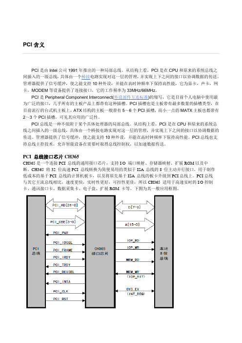
PCI含义PCI是由Intel公司1991年推出的一种局部总线。
从结构上看,PCI是在CPU和原来的系统总线之间插入的一级总线,具体由一个桥接电路实现对这一层的管理,并实现上下之间的接口以协调数据的传送。
管理器提供了信号缓冲,使之能支持10种外设,并能在高时钟频率下保持高性能,它为显卡,声卡,网卡,MODEM等设备提供了连接接口,它的工作频率为33MHz/66MHz。
PCI是Peripheral Component Interconnect(外设部件互连标准)的缩写,它是目前个人电脑中使用最为广泛的接口,几乎所有的主板产品上都带有这种插槽。
PCI插槽也是主板带有最多数量的插槽类型,在目前流行的台式机主板上,ATX结构的主板一般带有5~6个PCI插槽,而小一点的MATX主板也都带有2~3个PCI插槽,可见其应用的广泛性。
PCI总线是一种不依附于某个具体处理器的局部总线。
从结构上看,PCI是在CPU和原来的系统总线之间插入的一级总线,具体由一个桥接电路实现对这一层的管理,并实现上下之间的接口以协调数据的传送。
管理器提供了信号缓冲,使之能支持10种外设,并能在高时钟频率下保持高性能。
PCI总线也支持总线主控技术,允许智能设备在需要时取得总线控制权,以加速数据传送。
PCI 总线接口芯片CH365CH365是一个连接PCI 总线的通用接口芯片,支持I/O 端口映射、存储器映射、扩展ROM以及中断。
CH365 将32 位高速PCI 总线转换为简便易用的类似于ISA 总线的8 位主动并行接口,用于制作低成本的基于PCI 总线的计算机板卡,以及将原先基于ISA 总线的板卡升级到PCI总线上。
PCI总线与其它主流总线相比,速度更快,实时性更好,可控性更佳,所以CH365 适用于高速实时的I/O控制卡、通讯接口卡、数据采集卡、电子盘、扩展ROM 卡等。
下图为其一般应用框图。
引脚功能。
普瑞蓝功率芯片自制中文规格书

普瑞蓝功率芯片规格书BXCE45×45MILB XCE 45 x 45 mil 特点•高流明输出和效率•使用寿命长•增加目前蔓延痕迹高效和统一的照明•100%测试和排序的波长,功率与正向电压•朗伯发射模式•兼容焊锡膏,焊锡瓶坯或银环氧裸片粘接•交付中等粘性的蓝色胶带(20CM±为10mm×20厘米±10MM)应用范围•普通照明•路灯•便携式照明•建筑照明•定向照明•广域照明•显示背光•数码相机闪光灯•汽车照明•白光LEDLED芯片结构图产品命名方式:B XC E 4 5 4 5 X X X – Y Y – ZBXCE:指定产品系列4545:指定芯片尺寸(45 MIL×45 MIL)XXX:指定主导波长YY:指定辐射功率Z:指定正向电压机械尺寸6。
磁带应存放在垂直方向,而不是水平堆放。
磁带堆叠可以放置过大的压力,对LED的焊盘,导致焊线实力降低。
环保法规:普瑞致力于固态照明市场提供环保产品。
普瑞BXCE4545蓝色功率芯片是符合欧盟对电子设备的指令,即RoHS指令对有害物质的限制。
普瑞不会故意对BXCE4545模具产品添加以下限制材料:铅,汞,镉,六价铬,多溴联苯(PBB)或多溴二苯醚(PBDE)关于普瑞:普瑞是由40亿美金升值到100亿美金的全球照明行业的技术和解决方案的领先开发商和制造商。
总部设在加利福尼亚州利弗莫尔,普瑞是固态照明(SSL)的先驱,发光二极管(LED)技术,扩大市场,拉低了LED照明系统的成本。
普瑞的专利灯源技术取代与整合,固态照明解决方案,使灯具和照明设备制造商,以高的性能和迅速增长的能源效率的白色光(如白炽灯,卤素灯,荧光灯和高强度放电照明)传统技术内部和外部照明市场,包括路灯,商业照明和消费电子应用。
普瑞是与500多个专利申请或授予全球唯一垂直整合的LED制造商和专门开发固态光源照明行业设计的解决方案。
采用 DSP+FPGA 的三轴运动控制器设计
采用 DSP+FPGA 的三轴运动控制器设计何远松;谢明红【摘要】In order to meet the demand of open CNC system,a general three-axis motion controller was designed based on TMS320F28335 floating-point digital signal processor (DSP)and EP2C8F256C6 field programmable gate array (FP-GA).The overall structure of motion controller,the design of hardware circuits,the interpolation algorithm as well as the compostion and realization of FPGA modules were introduced in details,and the relevant design software structure dia-gram was presented accordingly.The motion controller has the characteristics of simple framework,high versatility and modularization,and can well meet the real-time and the accuracy of the motion control system.%为了满足开放式数控系统的需求,设计了一种基于 TMS320F28335浮点型数字信号处理器(DSP)和EP2C8F256C6现场可编程门阵列(FPGA)的通用三轴运动控制器。
详细介绍该运动控制器的整体结构、硬件电路设计、插补算法、FPGA 各分模块的构成及实现,并给出了相关设计的软件结构框图。
CH365P
类型 输入
引脚说明
MODEM 信号,清除发送,低电平有效,内置弱上拉 CH438Q 没有该引脚
41-43,45,58, 115-119,121,126,127
47 48
引脚名称 VCC GND
NC.
XI XO
类型 电源 电源
空脚
输入 输出
引脚说明 正电源端 公共接地端
禁止连接
晶体振荡的输入端,需要外接晶体及振荡电容 晶体振荡的反相输出端,需要外接晶体及振荡电容
4.2. 单片机接口信号线
引脚号 104
输出 输出 输出
4
MODEM 信号,数据终端就绪,低电平有效 CH438Q 没有该引脚
MODEM 信号,请求发送,低电平有效 CH438Q 没有该引脚
异步串行数据输出
5、内部时钟配置
CH438 芯片内部具有时钟振荡器,只需要在 XI 和 XO 引脚之间连接一个晶体,并且为 XO 引脚对
地连接振荡电容,就能产生串口所需的外部时钟信号,如果不接晶体和电容,CH438 芯片也可以通过
引脚名称 RST#
122
AMOD
107-114
7-13 7 124 125 123 103
D7~D0
A6~A0 ALE RD# WR# CS# INT
类型 输入
输入
三态输出 及输入 输入 输入 输入 输入 输入 开漏输出
引脚说明 外部手工复位输入,低电平有效,内置弱下拉电阻
地址输入方式选择: 低电平为直接地址方式,高电平为复用地址方式
LNK625DG;LNK623DG;LNK623PG;LNK625PG;LNK626PG;中文规格书,Datasheet资料

LNK623-626LinkSwitch-CV Family September 2009Energy-Effi cient, Off-line Switcher with Accurate Primary-side Constant-Voltage (CV) Control®Output Power TableProduct 3230 VAC ±15%85-265 VAC Adapter 1Peak or Open Frame 2Adapter 1Peak or Open Frame 2LNK623PG/DG 6.5 W 9 W 5.0 W 6 W LNK624PG/DG 7 W 11 W 5.5 W 6.5 W LNK625PG/DG 8 W 13.5 W 6.5 W 8 W LNK626PG/DG10.5 W17 W8.5 W10 WTable 1. Output Power Table. Based on 5 V Output. Notes:1. Minimum continuous power in a typical non-ventilated enclosed adapter measured at +50 °C ambient.2. Maximum practical continuous power in an open frame design with adequate heatsinking, measured at 50 °C ambient (see Key Application Considerations section for more information).3. Packages: P: DIP-8C, D: SO-8C.Product HighlightsDramatically Simplifi es CV Converters• Eliminates optocoupler and all secondary CV control circuitry • Eliminates bias winding supply – IC is self biasingAdvanced Performance Features• Compensates for external component temperature variations • Very tight IC parameter tolerances using proprietary trimming technology• Continuous and/or discontinuous mode operation for design fl exibility• Frequency jittering greatly reduces EMI fi lter cost• Even tighter output tolerances achievable with external resistor selection/trimming Advanced Protection/Safety Features• Auto-restart protection reduces delivered power by >95% for output short circuit and all control loop faults (open and shorted components)• Hysteretic thermal shutdown – automatic recovery reduces power supply returns from the fi eld• Meets HV creepage requirements between Drain and all other pins, both on the PCB and at the package EcoSmart ® – Energy Effi cient• No-load consumption <200 mW at 230 VAC and down to below 70 mW with optional external bias • Easily meets all global energy effi ciency regulations with no added components• ON/OFF control provides constant effi ciency down to very light loads – ideal for mandatory EISA and ENERGY STAR 2.0 regulations• No primary or secondary current sense resistors – maximizes effi ciency Green Package• Halogen free and RoHS compliant packageApplications • DVD/STB • Adapters• Standby and auxiliary supplies• Home appliances, white goods and consumer electronics • Industrial controlsDescriptionThe LinkSwitch-CV dramatically simplifies low power, constant voltage (CV) converter design through a revolutionary control technique which eliminates the need for both an optocoupler and secondary CV control circuitry while providing very tight output voltage regulation. The combination of proprietary IC trimming and E-Shield™ transformer construction techniques enables Clampless™ designs with the LinkSwitch-CV LNK623/4.Figure 1. Typical Application Schematic (a) and Output Characteristic Envelope (b).*Optional with LNK623-624PG/DG. (see Key Application Considerations section forclamp and other external circuit design considerations).LinkSwitch-CV provides excellent cross-regulation for multiple-output flyback applications such as DVDs and STBs. A 700 V power MOSFET and ON/OFF control state machine, self-biasing, frequency jittering, cycle-by-cycle current limit, and hysteretic thermal shutdown circuitry are all incorporated onto one IC.Rev. E 09/09Pin Functional DescriptionDRAIN (D) Pin:This pin is the power MOSFET drain connection. It provides internal operating current for both start-up and steady-state operation.BYPASS (BP) Pin:This pin is the connection point for an external bypass capacitor for the internally generated 6 V supply.FEEDBACK (FB) Pin:During normal operation, switching of the power MOSFET is controlled by this pin. This pin senses the AC voltage on the bias winding. This control input regulates the output voltage based on the fl yback voltage of the bias winding.SOURCE (S) Pin:This pin is internally connected to the output MOSFET source for high voltage power and control circuit common returns.Figure 2 Functional Block Diagram.Figure 3. Pin Confi guration.Rev. E 09/09LinkSwitch-CV Functional DescriptionThe LinkSwitch-CV combines a high voltage power MOSFET switch with a power supply controller in one device. Similar to the LinkSwitch-LP and TinySwitch-III it uses ON/OFF control to regulate the output voltage. The LinkSwitch-CV controllerconsists of an oscillator, feedback (sense and logic) circuit, 6 V regulator, over-temperature protection, frequency jittering, current limit circuit, leading-edge blanking, and ON/OFF state machine for CV control.Constant Voltage (CV) OperationThe controller regulates the feedback pin voltage to remain at V FBth using an ON/OFF state-machine. The feedback pinvoltage is sampled 2.5 μs after the turn-off of the high voltage switch. At light loads the current limit is also reduced to decrease the transformer fl ux density. Auto-Restart and Open-Loop ProtectionIn the event of a fault condition such as an output short or an open loop condition the LinkSwitch-CV enters into an appropriate protection mode as described below.In the event the feedback pin voltage during the Flyback period falls below V FBth -0.3 V before the feedback pin sampling delay (~2.5 μs) for a duration in excess of 200 ms (auto-restart on-time (t AR-ON ) the converter enters into Auto-restart, wherein the power MOSFET is disabled for 2.5 seconds (~8% Auto-Restart duty cycle). The auto-restart alternately enables and disables the switching of the power MOSFET until the fault condition is removed.In addition to the conditions for auto-restart described above, if the sensed feedback pin current during the Forward period of the conduction cycle (switch “on” time) falls below 120 μA, theconverter annunciates this as an open-loop condition (topresistor in potential divider is open or missing) and reduces the Auto-restart time from 200 ms to approximately 6 clock cycles (90 μs), whilst keeping the disable period of 2.5 seconds. This effectively reduces the Auto-Restart duty cycle to less than 0.01%.Over-Temperature ProtectionThe thermal shutdown circuitry senses the die temperature. The threshold is set at 142 °C typical with a 60 °C hysteresis. When the die temperature rises above this threshold (142 °C) the power MOSFET is disabled and remains disabled until the die temperature falls by 60 °C, at which point the MOSFET is re-enabled.Current LimitThe current limit circuit senses the current in the power MOSFET. When this current exceeds the internal threshold(I LIMIT ), the power MOSFET is turned off for the remainder of that cycle. The leading edge blanking circuit inhibits the current limit comparator for a short time (t LEB ) after the power MOSFET is turned on. This leading edge blanking time has been set so that current spikes caused by capacitance and rectifi er reverse recovery time will not cause premature termination of the MOSFET conduction.6.0 V RegulatorThe 6 V regulator charges the bypass capacitor connected to the BYPASS pin to 6 V by drawing a current from the voltage on the DRAIN, whenever the MOSFET is off. The BYPASS pin is the internal supply voltage node. When the MOSFET is on, the device runs off of the energy stored in the bypass capacitor. Extremely low power consumption of the internal circuitry allows the LinkSwitch-CV to operate continuously from the current drawn from the DRAIN pin. A bypass capacitor value of 1 μF is suffi cient for both high frequency decoupling and energy storage.Rev. E 09/09Applications ExampleCircuit DescriptionThis circuit is confi gured as a three output, primary-side regulated fl yback power supply utilizing the LNK626PG. It can deliver 7 W continuously and 10 W peak (thermally limited) from an universal input voltage range (85 – 265 VAC). Effi ciency is >67% at 115 VAC/230 VAC and no-load input power is <140 mW at 230 VAC.Input FilterAC input power is rectifi ed by diodes D1 through D4. The rectifi ed DC is fi ltered by the bulk storage capacitors C1 and C2. Inductor L1, L2, C1 and C2 form a pi (π) fi lter, which attenuates conducted differential-mode EMI noise. This confi guration along with Power Integrations transformerE-shield ™ technology allow this design to meet EMI standard EN55022 class B with good margin without requiring aY capacitor. Fuse F1 provides protection against catastrophic failure. Negative temperature coeffi cient thermistor RT1 limits the inrush current when AC is fi rst applied to below themaximum rating of diodes D1 through D4. Metal oxide varistor RV1 clamps the AC input during differential line transients, protecting the input components and maintaining the peakdrain voltage of U1 below its 700 V BV DSS rating. For differential surge levels at or below 2 kV this component may be omitted.LNK626 PrimaryThe LNK626PG device (U1) incorporates the power switching device, oscillator, CV control engine, startup, and protectionfunctions. The integrated 700 V MOSFET provides a large drain voltage margin in universal input AC applications, increasing reliability and also reducing the output diode voltage stress by allowing a greater transformer turns ratio. The device can be completely self-powered from the BYPASS pin and decoupling capacitor C4. In this design a bias circuit (D6, C6 and R4) was added to reduce no load input power below 140 mW.The rectifi ed and fi ltered input voltage is applied to one side of the primary winding of T1. The other side of the transformer’s primary winding is driven by the integrated MOSFET in U1. The leakage inductance drain voltage spike is limited by the clamp circuit D5, R1, R2, C3 and VR1. The zener bleed clamparrangement was selected for lowest no-load input power but in applications where higher no-load input power is acceptable VR1 may be omitted and the value of R1 increased to form a standard RCD clamp.Output Rectifi cationThe secondaries of the transformer are rectifi ed by D7, D8 and D9. A Schottky barrier type was used for the main 5 V output for higher effi ciency. The +12 V and -22 V outputs use an ultrafast rectifi er diode. The main output is post fi ltered by L3 and C10 to remove switching frequency ripple. Resistors R7, R8 and R9 provide a preload to maintain the output voltages within their respective limits when unloaded. To reduce high frequency ringing and associated radiated EMI an RC snubber formed by R10 and C13 was added across D7.Figure 4. 7 W (10 W peak) Multiple Output Flyback Converter for DVD Applications with Primary Sensed Feedback.Rev. E 09/09Output RegulationThe LNK626 regulates the output using ON/OFF control, enabling or disabling switching cycles based on the sampled voltage on the FEEDBACK pin. The output voltage is sensed using a primary referenced winding on transformer T1 eliminating the need for an optocoupler and a secondary sense circuit. The resistor divider formed by R3 and R6 feeds the winding voltage into U1. Standard 1% resistor values were used to center the nominal output voltages. Resistor R5 and C5 reduce pulse grouping by creating an offset voltage that is proportional to the number of consecutive enabled switching cycles. Key Application ConsiderationsOutput Power TableThe data sheet maximum output power table (Table 1)represents the maximum practical continuous output power level that can be obtained in a Flyback converter under the following assumed conditions:1. The minimum DC input voltage is 100 V or higher at 90 VACinput. The value of the input capacitance should be large enough to meet these criteria for AC input designs.2. Secondary output of 5 V with a Schottky rectifi er diode.3. Assumed effi ciency of 80%.4. Continuous conduction mode operation (K P = 0.4).5. Refl ected Output Voltage (V OR ) of 110 V .6. The part is board mounted with SOURCE pins soldered to asuffi cient area of copper to keep the SOURCE pin tempera-ture at or below 110 °C for P package and 100 °C for D packaged devices.7. Ambient temperature of 50 °C for open frame designs andan internal enclosure temperature of 60 °C for adapter designs.Note: Higher output power are achievable if the effi ciency is higher than 80%, typically for high output voltage designs.Bypass Pin CapacitorA 1 μF Bypass pin capacitor (C4) is recommended. The capacitor voltage rating should be equal to or greater than 6.8 V. The capacitor’s dielectric material is not important. The capacitor must be physically located close to the LinkSwitch-CV BYPASS pin.Circuit board layoutLinkSwitch-CV is a highly integrated power supply solution that integrates on a single die, both the controller and the highvoltage MOSFET. The presence of high switching currents and voltages together with analog signals makes it especiallyimportant to follow good PCB design practice to ensure stable and trouble free operation of the power supply.When designing a board for the LinkSwitch-CV based power supply, it is important to follow the following guidelines:Single Point GroundingUse a single point (Kelvin) connection at the negative terminal of the input fi lter capacitor for the LinkSwitch-CV SOURCE pin and bias winding return. This improves surge capabilities by returning surge currents from the bias winding directly to the input fi lter capacitor. Bypass CapacitorThe BYPASS pin capacitor should be located as close as possible to the SOURCE and BYPASS pins.Feedback ResistorsPlace the feedback resistors directly at the FEEDBACK pin of the LinkSwitch-CV device. This minimizes noise coupling.Thermal ConsiderationsThe copper area connected to the source pins provide the LinkSwitch-CV heat sink. A rule of thumb estimate is that the LinkSwitch-CV will dissipate 10% of the output power. Provide enough copper area to keep the source pin temperature below 110° C to provide margin for part to part R DS(ON) variation.Secondary Loop AreaTo minimize leakage inductance and EMI, the area of the loop connecting the secondary winding, the output diode and the output fi lter capacitor should be minimized. In addition, suffi cient copper area should be provided at the anode and cathode terminal of the diode for heatsinking. A larger area is preferred at the quiet cathode terminal. A large anode area can increase high frequency radiated EMI.Electrostatic Discharge Spark GapIn chargers and adapters ESD discharges may be applied to the output of the supply. In these applications the addition of a spark gap is recommended. A trace is placed along theisolation barrier to form one electrode of a spark gap. The other electrode, on the secondary side, is formed by the output return node. The arrangement directs ESD energy from the secondary to the primary side AC input. A 10 mil gap is placed near the AC input. The gap decouples any noise picked up on the spark gap trace to the AC input. The trace from the AC input to the spark gap electrode should be spaced away from other traces to prevent unwanted arcing occurring and possible circuit damage.Rev. E 09/096Figure 5. PCB Layout Example.Figure 6. Schematic Representation of Recommended Layout Without External Bias.Figure 7. Schematic Representation of Recommended Layout WithExternal Bias.+-AC INPI-5269-122408Y1-Capacitor(optional)Isolation Barrier TransformerT1Output RectifiersPrimary SideSecondary SideR1JP1J1C1R3R4C12R10D9C11C13D7C9R9R8D816R7C8L3C10C2R2C3D1D3D5VR1D6C6R6R5C5C4D4RV1F1D2RT1L2L1J2Input Filter Capacitor Drain trace area miniminzed ClampComponentsCopper area maximized for heatsinkingDC OutputsESD spark gapBypass Capacitor close to device Feedback Resistors close to device10 mil gapU1SFB BP D S S S Output Filter CapacitorRev. E 09/09Figure 8. Schematic Representation of Electrical Impact of Improper Layout.Rev. E 09/09Drain ClampRecommended Clamp CircuitsComponents R1, R2, C3, VR1 and D5 in fi gure 4 comprise the clamp. This circuit is preferred when the primary leakage inductance is greater than 125 μH to reduce drain voltageovershoot or ringing present on the feedback winding. For best output regulation, the feedback voltage must settle to within 1% at 2.1 μs from the turn off of the primary MOSFET. This requires careful selection of the clamp circuit components. The voltage of VR1 is selected to be ~20% above the refl ected output voltage (V OR ). This is to clip any turn off spike on the drain but avoid conduction during the fl yback voltage interval when the output diode is conducting. The value of R1 should be the largest value that results in acceptable settling of the feedback pin voltage and peak drain voltage. Making R1 too large will increase the discharge time of C3 and degrade regulation. Resistor R2dampens the leakage inductance ring. The value must be large enough to dampen the ring in the required time but must not be too large to cause the drain voltage to exceed 680 V.If the primary leakage inductance is less than 125 μH, VR1 can be eliminated and the value of R1 increased. A value of 470 k Ω with an 820 pF capacitor is a recommended starting point. Verify that the peak drain voltage is less than 680 V under all line and load conditions. Verify the feedback winding settles to an acceptable limit for good line and load regulation.Effect of Fast (500 ns) versus Slow (2 μs) RecoveryDiodes in Clamp Circuit on Pulse Grouping and Output Ripple.A slow reverse recovery diode reduces the feedback voltage ringing. The amplitude of ringing with a fast diode represents 8% error in Figure 10.Figure 9. RCD Clamp, Low Power or Low Leakage Inductance Designs. RCD Clamp With Zener Bleed. High Power or High Leakage Inductance Designs.Figure 10. Effect of Clamp Diode on Feedback Pin Settling. Clamp Circuit (top). Feedback Pin Voltage (bottom).Black Trace: D C1 is a FR107 (fast type, trr = 500 ns)Gray Trace: D C1 is a 1N4007G (standard recovery, trr = 2 us)Rev. E 09/09Figure 11. Not Pulse Grouping (<5 Consecutive Switching Cycles).Pulse Grouping (>5 Consecutive Switching Cycles).Top Trace: Drain Waveform (200 V/div)Bottom Trace: Output Ripple Voltage (50 mV/div)Split Screen with Bottom Screen Zoom Top Trace: Drain Waveform (200 V/div)Bottom Trace: Output Ripple Voltage (50 mV/div)Clampless DesignsClampless designs rely solely on the drain node capacitance to limit the leakage inductance induced peak drain-to-sourcevoltage. Therefore the maximum AC input line voltage, the value of V OR , the leakage inductance energy, (a function of leakage inductance and peak primary current), and the primary winding capacitance determine the peak drain voltage. With no signifi -cant dissipative element present, as is the case with an external clamp, the longer duration of the leakage inductance ringing can increase EMI.The following requirements are recommended for a universal input or 230 VAC only Clampless design:1. Clampless designs should only be used for P O ≤5 W using aV OR of ≤90 V2. For designs with P O ≤5 W, a two-layer primary must be usedto ensure adequate primary intra-winding capacitance in the range of 25 pF to 50 pF . A bias winding must be added to the transformer using a standard recovery rectifi er diode(1N4003– 1N4007) to act as a clamp. This bias winding may also be used to externally power the device by connecting a resistor from the bias winding capacitor to the BYPASS pin. This inhibits the internal high-voltage current source, reducing device dissipation and no-load consumption.3. For designs with P O >5 W, Clampless designs are not practicaland an external RCD or Zener clamp should be used.4. Ensure that worst-case, high line, peak drain voltage is belowthe BV DSS specifi cation of the internal MOSFET and ideally ≤650 V to allow margin for design variation.V OR (Refl ected Output Voltage), is the secondary output plus output diode forward voltage drop that is refl ected to the primary via the turns ratio of the transformer during the diode conduction time. The V OR adds to the DC bus voltage and the leakage spike to determine the peak drain voltage.Pulse GroupingPulse grouping is defi ned as 6 or more consecutive pulses followed by two or more timing state changes. The effect of pulse grouping is increased output voltage ripple. This isshown on the right of Figure 11 where pulse grouping has caused an increase in the output ripple.To eliminate group pulsing verify that the feedback signal settles within 2.1 μs from the turn off of the internal MOSFET. A Zener diode in the clamp circuit may be needed to achieve the desired settling time. If the settling time is satisfactory, then a RC network across R LOWER (R6) of the feedback resistors is necessary.The value of R (R5 in the Figure 12) should be an order of magnitude greater than R LOWER and selected such that R×C = 32 μs where C is C5 in Figure 12.Quick Design ChecklistAs with any power supply design, all LinkSwitch-CV designs should be verifi ed on the bench to make sure that component specifi cations are not exceeded under worst-case conditions.Figure 12. RC Network Across R BOTTOM (R6) to Reduce Pulse Grouping.Rev. E 09/09The following minimum set of tests is strongly recommended:1. Maximum drain voltage – Verify that peak V DS does not exceed680 V at highest input voltage and maximum output power. 2. Maximum drain current – At maximum ambient temperature,maximum input voltage and maximum output load, verify drain current waveforms at start-up for any signs of trans-former saturation and excessive leading edge current spikes. LinkSwitch-CV has a leading edge blanking time of 215 ns to prevent premature termination of the ON-cycle. Verify that the leading edge current spike is below the allowed current limit envelope for the drain current waveform at the end of the 215 ns blanking period.3. Thermal check – At maximum output power, both minimumand maximum input voltage and maximum ambient tempera-ture; verify that temperature specifi cations are not exceeded for LinkSwitch-CV , transformer, output diodes and output capacitors. Enough thermal margin should be allowed for the part-to-part variation of the R DS(ON) of LinkSwitch-CV , as specifi ed in the data sheet. It is recommended that the maximum source pin temperature does not exceed 110 °C.Design ToolsUp-to-date information on design tools can be found at the Power Integrations web site: 分销商库存信息:POWER-INTEGRATIONSLNK625DG LNK623DG LNK623PG LNK625PG LNK626PG LNK624DG LNK623DG-TL LNK624DG-TL LNK624PG LNK625DG-TL LNK626DG-TL LNK626DG RDK-201。
Uniwell LX-5600 LX-5700 LX-5750 Type 05商品说明书

Uniwell LX-5600 LX-5700 LX-5750 Type 05 Programming ManualProgramming Manualfor 05 Type2-sheet dot matrix printer EX-560/LX-5600/PX-6600/*2-sheet thermal printer EX-570/LX-5700/PX-6700/PX-57001-sheet thermal printer EX-575/LX-5750/PX-6750/PX-5750*There is no dot matrix printer model for PX-5000 series.CAUTION!When the control key position is LOCK, the display is off andkeyboard is disabled but the ECR's power is still ON.So that before you open the upper case, make sure that thepower switch is turned OFF. Especially when you replace theROM, it must be turned off, otherwise the ECR will be damaged.CONTENTS OF PROGRAMMING MANUALI.BEFORE INSTALLATION (5)II.INTRODUCTION (6)III.SPECIFICATIONS (7)Hardware (7)System Configuration (8)RAM Board Expansion (9)Options (9)Set-up of Peripherals (9)IV.STANDARD KEY LAYOUT (10)V.PROGRAMMING (13)KEYBOARD PROGRAMMING (14)(SP-101) KEY LAYOUT (14)PLU & GROUP PROGRAMMING (18)Concerning PLU and Group Programming (18)User friendly PLU programming in "R" position (20)User friendly PLU programming in "SP" position (21)(SP-201/4201) PLU CODE (22)(SP-203/4203) PLU LINK TO GROUP (23)(Z1/P-5302) PLU NAME & PRICE (24)(Z1/P-305/4305) PLU PRICE (24)(Z1/P-320/4320) PLU HALO (High Amount Lock-Out) (25)(SP-111) PLU LINK TO HARD PLU KEY (25)(SP-200/4200) PLU FUNCTION FLAG (25)(SP-207) PLU LINK TO QUNATITY DISCOUNT TABLE (28)(SP-208) PLU LINK TO R. PLU (28)(SP-209/4209) PLU LINK TO SUPPLEMENTARY MESSAGE (28)(SP-223/4223) GROUP-A LINK TO MAIN GROUP-A (28)(SP-117) R. PLU QUANTITY FOR PACKED SALE KEYS (29)(Z2-406) PLU STOCK (29)(SP-5201) COMPLETE PLU PROGRAMMING (30)(SP-298) AGE TABLE (31)(SP-127) TARE TABLE (31)QUANTITY DISCOUNT TABLE PROGRAMMING (32)(SP-280/4280) QUANTITY DISCOUNT FUNCTION (33)(Z1/P-381) QUANTITY IN BUCKET (34)(Z1/P-385) BUCKET PRICE / DISCOUNT PRICE / DISCOUNT % (34)(SP-5282) COMPLETE QUANTITY DISCOUNT PROGRAMMING (34)R. PLU PROGRAMMING (35)(Z1/P-375) R. PLU PRICE (35)(SP-273/4273) R. PLU LINK TO GROUP (35)(SP-270/4270) R. PLU FUNCTION (35)(SP-5272) COMPLETE R. PLU PROGRAMMING (36)CHARACTER PROGRAMMING (37)(SP-212) CASHIER NAME (37)(SP-222) GROUP-A NAME (37)(SP-232) GROUP-B NAME (37)(SP-102) KEY/SYMBOL NAME (37)(SP-242) MAIN GROUP-A NAME (37)(SP-252) MEDIA NAME (37)(SP-262) MEDIA CURRENCY SYMBOL (37)(SP-202) PLU NAME (37)(SP-282) QUANTITY DISCOUNT TABLE NAME (37)(SP-272) R. PLU NAME (37)(SP-122) RECEIPT LOGO (37)(SP-162) SLIP/VALIDATION LOGO (37)(SP-142) SUPPLEMENTARY MESSAGE (37)(SP-182) WARNING MESSAGE (37)(SP-131) CHARACTER KEY LAYOUT FOR SETTING NAMES (46)RATE PROGRAMMING (49)(Z1/P-337) PERCENTAGE RATE (49)(Z1/P-347) ADJUSTMENT RATE (49)(Z1/P-387) FOREIGN CURRENCY EXCHANGE RATE (49)(Z1/P-377) CHEQUE-CASHING CHARGE RATE / CURRENCY EXCHANGE CHARGE RATE (50)(Z1/P-397) EURO CURRENCY RATE (50)(SP-107) TAX RATE (50)(SP-108) TAX EXEMPTION LIMIT FOR % TAX / TAX TABLE FOR ADD-ON TAX SYSTEM (51)MEDIA PROGRAMMING (54)(Z1/P-310) TOTAL HALO (54)(SP-253) PRESET TENDER KEY LINK TO MEDIA (54)(Z1/P-315) PRESET TENDER AMOUNT (55)(SP-110) MEDIA FUNCTION (55)CASHIER PROGRAMMING (58)(SP-211) SECRET CASHIER CODE (58)(SP-221) CASHIER CARD NUMBER (58)(SP-213) CASHIER LINK TO iBUTTON (58)(SP-210) CASHIER SECURITY FUNCTION (59)MISCELLANEOUS PROGRAMMING (60)(SP-151) TRAINING SECRET CODE (60)(SP-161) FLAG SET WITHOUT X KEY (60)(SP-171) MACHINE NUMBER (60)(SP-172) TERMINAL ADDRESS (60)(SP-121) ARRANGEMENT KEY SEQUENCE (61)(SP-189) CHEQUE PRINTING FORMAT (62)(SP-181/4181) ESF DATA SELECTION (65)(SP-191) BAR CODE ON RECEIPT [SF-63.a=1] for Thermal Printer (67)TIME & DATE PROGRAMMING (69)(X-1) DATE (69)(X-2) TIME (69)SYSTEM PROGRAMMING (70)(SP-100) SYSTEM FUNCTION (70)DATA OF CARD PROGRAMMING (100)1. Adjustment Card and Amount Track Card (100)2. Arrangement Card (101)CUSTOMER FILE PROGRAMMING (102)1. Outline (102)2. Operation Sequences (103)PROGRAMMING REFERENCE (104)VI.REPORTS (107)REPORT SEQUENCE (107)IRC REPORT SEQUENCE (111)FLASH IRC REPORTS (113)PROGRAM DUMP CONTENTS (114)VII.SERVICE PROGRAMMING (119)INITIAL RESET (119)TEST PROGRAMS (120)RAM TEST SP-9901 (120)PHYSICAL RAM TEST (121)ROM TEST SP-9902 (121)PLU DATA ERASE SP-289 (121)TEST PRINT SP-9909 (121)HARDWARE TEST SP-9998/9999 (122)AUTO PRESET (124)IRC PROGRAM DATA TRANSFER (126)VIII.WARNING MESSAGES (128)IX.IRC MESSAGES (131)This is a “Table of Contents preview” for quality assuranceThe full manual can be found at /estore/catalog/ We also offer free downloads, a free keyboard layout designer, cable diagrams, free help andsupport. : the biggest supplier of cash register and scale manuals on the net。
Hittite Microwave Corporation HMC365G8分频器产品说明书

THIS PAGE INTENTIONALLY LEFT BLANK4For price, delivery and to place orders: Hittite Microwave Corporation, 20 Alpha Road, Chelmsford, MA 01824Phone: 978-250-3343 Fax: 978-250-3373 Order On-line at ApplicationSupport:Phone:******************************General Description Functional Diagram The HMC365G8 is a low noise Divide-by-4 Static Divider with InGaP GaAs HBT technology in an 8 lead glass/metal (hermetic) surface mount hermetic package. This device operates from DC (with a square wave input) to 13 GHz input frequency with a single +5V DC supply. The low additive SSB phase noiseof -151 dBc/Hz at 100 kHz offset helps the user maintain good system noise performance.Ultra Low SSB Phase Noise: -151 dBc/Hz Wide Bandwidth Output Power: 7 dBm Single DC Supply: +5V 8 Lead Hermetic SMT Package Electrical Specifications, T A = +25° C, 50 Ohm System, Vcc = 5VPrescaler for DC to Ku Band PLL Applications:• Point-to-Point / Multi-Point Radios• VSAT Radios • Fiber Optic • Test Equipment • Space & Military1. Divider will operate down to DC for square-wave input signal.F R E Q U E N C Y D I V I D E R S & D E T E C T O R S - S M T 44 - 2For price, delivery and to place orders: Hittite Microwave Corporation, 20 Alpha Road, Chelmsford, MA 01824Phone: 978-250-3343 Fax: 978-250-3373 Order On-line at ApplicationSupport:Phone:******************************-30-20-100102001234567891011121314151617I N P U T P O W E R (d B m )INPUT FREQUENCY (GHz)-30-20-100102001234567891011121314151617Min Pin + 25C Max Pin + 25CMin Pin + 85CMax Pin + 85CMin Pin -40CMax Pin -40CI N P U T P O W E R (d B m )INPUT FREQUENCY (GHz)SSB Phase NoisePerformance, Pin= 0 dBm, T= 25 °C Output Power vs. Temperature Reverse Leakage, Pin= 0 dBm, T= 25 °COutput Harmonic Content, Pin= 0 dBm, T= 25 °C -160-140-120-100-80-60-40-200102103104105106107S S BP HASEN OIS E(dB c /H z)OFFSET FREQUENCY (Hz)-60-50-40-30-20-10003691215Both Output Ports Terminated One Output Port Terminated POW ERLE VEL(d Bm )INPUT FREQUENCY (GHz)-50-40-30-20-10003691215Pfeedthru 2nd Harmonic 3rd Harmonic O U T P U T L E V E L (d B m )INPUT FREQUENCY (GHz)024681003691215+ 25C + 85C - 40C O U T P U T P O W E R (d B m )INPUT FREQUENCY (GHz)4For price, delivery and to place orders: Hittite Microwave Corporation, 20 Alpha Road, Chelmsford, MA 01824Phone: 978-250-3343 Fax: 978-250-3373 Order On-line at ApplicationSupport:Phone:******************************Outline DrawingNote: Divider will operate over full voltage range shown above Typical Supply Current vs. Vcc3. PLATING: ELECTROLYTIC GOLD 50 MICROINCHES MIN., OVERELECTROLYTIC NICKEL 50 MICROINCHES MIN.4. DIMENSIONS ARE IN INCHES [MILLIMETERS].5. TOLERANCES: ±.005 [0.13] UNLESS OTHERWISE SPECIFIED.6. ALL GROUND LEADS AND GROUND PADDLE MUST BE SOLDERED TO PCB RF GROUND.ELECTROSTATIC SENSITIVE DEVICE OBSERVE HANDLING PRECAUTIONS -700-500-300-10010030050070022.723.123.523.924.324.7A M P L I T U D E (m V )TIME (nS)F R E Q U E N C Y D I V I D E R S & D E T E C T O R S - S M T 44 - 4For price, delivery and to place orders: Hittite Microwave Corporation, 20 Alpha Road, Chelmsford, MA 01824Phone: 978-250-3343 Fax: 978-250-3373 Order On-line at ApplicationSupport:Phone:******************************4For price, delivery and to place orders: Hittite Microwave Corporation, 20 Alpha Road, Chelmsford, MA 01824Phone: 978-250-3343 Fax: 978-250-3373 Order On-line at ApplicationSupport:Phone:******************************The circuit board used in the application should use RF circuit design techniques. Signal lines should have 50 Ohm impedance while the package ground leads and backside ground slug should be con-nected directly to the ground plane similar to that shown. A sufficient number of via holes should be used to connect the top and bottom ground planes.The evaluation circuit board shown is availablefrom Hittite upon request. This evaluation board isdesigned for single ended input testing. J2 and J3provide differential output signals.[1] Reference this number when ordering complete evaluation PCB[2] Circuit Board Material: Rogers 4350List of Materials for Evaluation PCB 106582 [1]F R E Q U E N C Y D I V I D E R S & D E T E C T O R S - S M T 44 - 6For price, delivery and to place orders: Hittite Microwave Corporation, 20 Alpha Road, Chelmsford, MA 01824Phone: 978-250-3343 Fax: 978-250-3373 Order On-line at ApplicationSupport:Phone:******************************。
富士 POD UG系列宏篇 UG00S-CWV4可编程序操作显示器 说明书

序言感谢您选择了富士可编程序操作显示器POD UG系列。
这个用户手册<宏篇>,解说UG系列用画面作成编辑器(UG00S-CWV4)的宏功能。
请认真阅读这本用户手册,正确使用机器。
另外,除这本手册以外还准备有下列UG系列手册。
请按照使用目的选择阅读。
手册名称手册编号记载内容UG00S-CWV4 设置篇FCH390解说画面作成编辑器(UG00S-CWV4)的安装方法UG00S-CWV4 功能篇FCH391解说画面作成编辑器(UG00S-CWV4)的各功能设定方法UG00S-CWV4 安装篇FCH393解说画面作成编辑器(UG00S-CWV4)的基本的操作方法UG00S-CWV4 操作篇FCH394解说画面作成编辑器(UG00S-CWV4)的操作方法UG00S-CWV4 指南篇FCH395解说UG系列的代表功能/使用方法UG20 Series <Hardware>FEH352解说UG520 / 420 / 320 / 221/220系列硬件UG Series <Variable NameFEH363解说UG编辑器和D300win的变量名协同功能Cooperation Function>UG Series <Temperature ControlFEH365解说温控网络功能Network>UG30 Series <Hardware>FEH377解说UG530 / 430 / 330系列硬件UG Series <PLC Connection>FEH380解说UG系列和各公司PLC的连接和通用串行通信等UG230 Series <Hardware>FEH381解说UG230系列硬件Simple POD <Hardware>FEH382解说Simple POD (UG221H-LE4, LR4, SR4)的硬件UG630 Series <Hardware>FEH389解说UG630系列硬件说明:1.富士电机机器控制公司拥有本软件的版权。
pro-face sp5000系列 硬件手册说明书

目录
SP5000-MM01-CS-PDF_O
安全信息 ....................................................................................................7 关于本书 ....................................................................................................8 概述......................................................................................................... 11
对于将本指南或其内容用作商业用途的行为,施耐德电气未授予任何权利或许可,但 以“原样”为基础进行咨询的非独占个人许可除外。
施耐德电气的产品和设备应由合格人员进行安装、操作、保养和维护。
由于标准、规格和设计会不时更改,因此本指南中包含的信息可能会随时更改,恕不 另行通知。
在适用法律允许的范围内,对于本资料信息内容中的任何错误或遗漏,或因使用此处 包含的信息而导致或产生的后果,施耐德电气及其附属公司不会承担任何责任或义 务。
标准主机模块 ................................................................................28 增强型主机模块............................................................................. 30 开放型主机模块............................................................................. 32 LED 指示 ......................................................................................34 显示模块 ............................................................................................35 精良显示模块 ................................................................................35 高级显示模块 ................................................................................39 LED 指示 ......................................................................................42 规格......................................................................................................... 44 一般规格 ............................................................................................44 电气规格....................................................................................... 44 环境规格....................................................................................... 46 结构规格....................................................................................... 47 功能规格 ............................................................................................49 显示规格....................................................................................... 49 存储器 ..........................................................................................51 时钟 .............................................................................................51 触摸屏 ..........................................................................................51 接口规格 ............................................................................................52 接口规格....................................................................................... 52 接口连接....................................................................................... 54 用于 COM1/COM2 的串行接口 (RS-232C 和 RS-422/RS485) .............................................................................................57 辅助输出/扬声器输出接口 (AUX) ....................................................59 DVI-D 输出接口.............................................................................60 尺寸......................................................................................................... 62 标准主机模块...................................................................................... 62 SP-5B00 ......................................................................................62 增强型主机模块 ..................................................................................63 SP-5B10 ......................................................................................63 开放型主机模块 ..................................................................................63
【国家自然科学基金】_平滑转换_基金支持热词逐年推荐_【万方软件创新助手】_20140730

1 1 1 1 1 1 1 1 1 1 1 1 1 1 1 1 1 1 1 1 1 1 1 1 1 1 1 1 1 1 1 1 1 1 1 1 1 1 1 1 1 1 1 1 1
53 54 55 56 57 58 59 60 61 62 63 64 65 66 67 68 69 70 71 72 73 74 75 76 77 78 79 80 81 82 83 84 85 86 87 88 89
53 54 55 56 57 58 59 60 61 62 63 64 65 66 67 68 69 70 71 72 73 74 75 76 77 78 79 80 81 82 83 84 85 86 87 88 89 90 91 92 93 94 95 96 97
模式切换 期货价格 数字滤波器 改进型遗传算法 捷联惯性导航系统 捕获跟踪 称调节 密度脉动 子阵 多模态控制 多分辨率分析 哮喘 咖啡因 同步定位与地图构建(slam) 受体,生长因子 双摆机器人 单目视觉 协方差矩阵 协整 动态补偿 加权求平均 功率平滑控制 初始对准 兰尼定 光电跟踪 信号转导 wald检验 vlbi suplm检验 smad3 rhoa monte carlo模拟 kalman滤波 itrf inside-out膜片 gps fp激光器 cell-attached膜片 bootstrap "类等效"建模
科研热词 非线性协整 非线性偏振旋转 转化生长因子-β 1 超快光学 误差修正 血管平滑肌细胞 胆石症 美国国库券收益率 细胞凋亡 糖皮质激素 点云 流定位 水平压力梯度误差 气道重塑 最小包含球问题 时移电视 数学形态学 支持向量回归 彩色空间转换 彩色图像分割 平滑卷积 展宽脉冲光纤激光器 大鼠 圆形印鉴 图像提取 哮喘 可视化仿真手术 反求工程 卡通招贴画 区域定位 加权矢量中值滤波 分裂合并 光纤激光器 信号通路 信号转导 三维重建 σ 坐标海洋模式 vcr操作 sup w检验 smad pom模式 mpeg2-ts e1a激活基因阻遏子 bootstrap
ch395技术指标

ch395技术指标
CH395技术指标是指CH395芯片的技术参数和规格。
CH395是一
款由中国科学院自动化研究所研发的高性能、低功耗的多核处理器。
它采用了先进的多核架构,集成了多种外设接口和功能模块,适用
于物联网、智能终端等领域。
从技术指标的角度来看,CH395的主要参数包括处理器核心数、主频、内存接口、外设接口、功耗等。
CH395多核处理器拥有多个
处理器核心,可以同时处理多个任务,提高系统的整体性能。
主频
则决定了处理器的运行速度,内存接口决定了处理器与内存之间的
数据传输速度。
外设接口包括了各种通信接口、存储接口等,可以
满足不同应用场景的需求。
此外,功耗也是一个重要的技术指标,
低功耗可以延长设备的续航时间,降低系统的热量和功耗。
从应用角度来看,CH395多核处理器可以应用于物联网设备、
智能终端、工业控制等多个领域。
它的多核架构和丰富的外设接口
使得它可以处理复杂的数据和多种传感器信息,满足不同应用场景
的需求。
同时,低功耗的特性也使得它在移动设备和无线传感器网
络中具有较好的应用前景。
总的来说,CH395技术指标包括处理器核心数、主频、内存接口、外设接口、功耗等多个方面,这些指标决定了CH395在不同应用场景下的性能和适用性。
通过了解CH395的技术指标,可以更好地评估其在特定应用场景下的表现和优势。
CH365中文手册(一)

SYS_EX (INT_REQ)
本地 8位 总线
2、特点
● 实现基于 32 位 PCI 总线的从设备接口。 ● 转换为主动并行接口:8 位数据,16 位地址,I/O 读和写,存储器读和写。 ● 可以设定 PCI 板卡的设备标识(Vendor ID,Device ID,Class Code 等)。 ● 支持以字节、字或双字为单位对 I/O 端口或者存储器进行读写。 ● 非突发存取的实测速度可达每秒 7MB,读写脉冲的宽度从 30nS 到 240nS 可选。 ● 自动分配 I/O 基址,支持长度达 240 字节的 I/O 端口。 ● 支持本地硬件定址功能,自由选择 I/O 地址,在指定地址实现 I/O 端口。 ● 直接升级 ISA 的 I/O 板卡到 PCI 总线,完全不需要修改原 ISA 卡的相关软件。 ● 直接映射支持容量为 32KB 的存储器 SRAM 或者扩展 ROM(Boot ROM)。 ● 无需外接元器件扩容支持容量为 64KB 以及 128KB 的存储器或者扩展 ROM。
WW WW WRRRRRRW WW WW RRRRRWWW WRRWRWWW RR (禁止使用)
复位后的默认值 连接到 I/O 设备
xxxxxxxx 000000xx (禁止使用) 连接到存储器
xxH 00000000
00H 00H rrrrr00x 0rr0r111 xxH (禁止使用)
6.4. 寄存器的位说明
6.2. 配置空间 0FFH-00H
类别
标准 PCI 设备 配置 空间
地址 01H-00H 03H-02H 05H-04H 07H-06H
08H 0BH-09H 0FH-0CH
13H-10H
17H-14H 2FH-18H 33H-30H
6815芯片工作原理

6815芯片工作原理6815芯片的主要工作原理是基于一种称为VLIW(Very Long Instruction Word)的指令集体系结构。
VLIW是一种指令并行处理的技术,它允许多个指令同时执行,极大地提高了芯片的运算能力。
在6815芯片中,CPU核心是其中最重要的模块,它负责执行指令、控制数据流动和完成各种运算操作。
CPU核心包括多个处理单元,可以同时执行多个指令。
这些指令可以是不同类型的指令,例如算术指令、逻辑指令、分支指令等。
通过同时执行多个指令,CPU核心能够提高芯片的处理能力,实现更高效的运算。
浮点运算单元是另一个重要的功能模块,它负责执行浮点运算操作。
浮点运算是一种对于小数点的数进行操作的方法,它广泛应用于科学计算、图像处理和语音识别等领域。
浮点运算单元通过专门的硬件电路,能够高效地完成复杂的浮点运算操作,提高了芯片的浮点运算能力。
存储器是芯片的另一个关键模块,它用于存储数据和指令。
存储器是芯片的“记忆”部分,它可以分为内部存储器和外部存储器两部分。
内部存储器是芯片内部集成的存储器,速度快但容量有限;外部存储器是外接的存储器,容量大但速度较慢。
存储器在芯片的运算过程中发挥着至关重要的作用,它能够存储各种数据和指令,为CPU核心提供必要的数据支持。
总线接口是连接芯片与外部设备的接口,它负责数据的输入和输出。
总线接口可以连接到各种外部设备,例如显示器、键盘、存储器等。
通过总线接口,芯片能够与外部设备进行数据交互,实现更丰富的功能。
综上所述,6815芯片的工作原理是基于VLIW指令集体系结构,通过多个功能模块的协调工作,实现数据的输入、处理和输出。
CPU核心执行指令,浮点运算单元执行浮点运算操作,存储器存储数据和指令,总线接口连接外部设备,完成各种功能。
这种工作原理使得6815芯片能够实现高性能的数字信号处理功能,广泛应用于移动通信领域。
- 1、下载文档前请自行甄别文档内容的完整性,平台不提供额外的编辑、内容补充、找答案等附加服务。
- 2、"仅部分预览"的文档,不可在线预览部分如存在完整性等问题,可反馈申请退款(可完整预览的文档不适用该条件!)。
- 3、如文档侵犯您的权益,请联系客服反馈,我们会尽快为您处理(人工客服工作时间:9:00-18:30)。
InterdisciplinaryHarmonising Rock Engineering and the Environment–Qian&Zhou(eds)©2012Taylor&Francis Group,London,ISBN978-0-415-80444-8A comprehensive approach in predicting excessive sand productionM.Bai,C.Santana&X.ShenHalliburton,Houston,TX,USABSTRACT:In contrast to the conventional approach of sanding prediction where only one particular method is selected(e.g., either empirical,analytical,numerical,or experimental),a comprehensive geomechanical approach is presented in this paper to predict excessive sand production,which includes:a)employing an analytical method with the combination of experience-based empirical rules and analytical expressions to assess the sand production risk under simplified conditions,b)performing a numerical study using the desired constitutive relationships in a three-dimensional field environment to examine wellbore and perforation device stability under the complex configurations and to validate the initial calculations,and c)conducting an experimental approach using laboratory-rock mechanical testing techniques to calibrate the sanding prediction under simulated downhole conditions.The presented approach uses the self-calibrated predictions on sand production via multiple methods, which can lead to a sensible decision for selecting effective and economical sand-control measures.The unified approach was illustrated in a case study where the critical drawdown pressure was sensibly determined by multiple methods.Subject:Petroleum geomechanicsKeywords:rock failure,stability analysis,weak rock1INTRODUCTIONA limited amount of sand production during hydrocarbon production in a form of fine migration is considered nor-mal.However,if the sand production exceeds certain level, a number of serious consequences may occur,varying from wellbore instability[Figure1(a)],sand cavity collapse[Fig-ure1(b)],and weak formation breakdown[Figure1(c)],to sand-prevention device failure[Figure1(d)].Without taking immediate remedial measures to prevent excessive sand pro-duction,normal hydrocarbon production would be severely hindered,or even terminated.Excessive sand production can directly affect well pro-duction and casing stability.Rock mechanical failure around the wellbore and near the perforation tunnels in poorly-consolidated sandstone formations subjected to aggressive hydrocarbon production appears to be the major cause of excessive sand production.Classical sand-control techniques are primarily based on the installation of sand exclusion devices,such as gravel packing,expandable screens,etc., which dramatically increase the completion cost and detrimen-tally reduce hydrocarbon production.As a result,it is desirable to predict excessive sanding potential and assess comple-tion device stability near perforation tunnels before a sensible decision can be made on whether or not to perform the costly sand-control procedures.Numerous sand prediction methods have currently been employed to assist in designing sand-prevention devices for completion and in determining the maximum depletion rate for a sand-free production.For predicting the critical draw-down pressure at the maximum bottomhole flowing pressure under the simple configurations,analytical and experience-based empirical methods are popular[Fjær et al.,(1992); Hettema et al.(2006);Willson et al.(2002);andYi(2003)].For predicting the stability of sand-prevention devices and perfo-ration tunnels with complex structural geometries,numerical methods,such as the finite element method,are generally preferred[Garolera et al.(2003);Wan and Wang(2003);and Figure1.Formation instability and sand exclusion device damage from excessive sand production.Zhang et al.(2007)].For calibrating the sanding prediction, experimental methods involving laboratory-rock mechanical testing are employed if the sample cores in the sand-prone formation are available[Nouri et al.(2004);and Core Lab (2003)].Using one particular method(e.g.,either analytical,empir-ical,numerical,or experimental)may be convenient,but it can lead to an incomplete or a biased analysis of sanding pre-diction.To avoid this shortcoming,the presented technique provides a unified approach that employs multiple methods with complementary objectives:a)analytical and empirical methods assess the sand-production risk under the simpli-fied conditions;b)numerical methods examine stability of sand prevention devices under realistic configurations;and c)experimental methods calibrate the sand predictions under simulated downhole conditions.In the present study,attentionFigure2.Critical bottomhole flowing pressure(CBHFP)versus reservoir pressure where the critical drawdown pressure(CDP)is constrained(CDP0is CDP at the initial reservoir pressure P RES,0). is focused on predicting the critical drawdown pressure(CDP) under tolerable sand production.2ANAL YTICAL&EMPIRICAL METHODSThe primary purpose of the analytical and empirical methods in this paper focuses on determining the critical drawdown pressure(CDP)constrained by the sand-free envelope.This envelope is generally shown in Figure2(i.e.,filled blue tri-angle area).The sand-free envelope is defined by the border lines of:a)an equal line between the critical bottomhole flow-ing pressure(CBHFP or P cwf)and reservoir pressure(RP or P RES),b)the critical drawdown pressure(CDP)at the current reservoir condition[e.g.,initial condition(P RES,0)or depleted condition(P RES)],and c)the minimum CBHFP,which can be expressedas:where,P cwf is the critical bottomhole flowing pressure(i.e., CBHFP),P RES is the reservoir pressure(i.e.,RP),a is the line slope between the minimum CBHFP and RP,and b is the magnitude of the line intersect.Equation1is the general form of the lower border line for the sand-free envelope.Fjær et al.(1992)proposed the following equation for calculating the critical drawdown pressure(CDP): where,UCS is the unconfined compressive strength,Cs is the cohesion,φis the internal friction angle,and n is an empirical coefficient that is related to the well flow geometry,as shown in Figure3.The empirical coefficient,n,ranges from1to2depending on whether it is an open hole(i.e.,n=1)or a cased hole(i.e., n=2).Sometimes,n is chosen as a variable between1and 2depending on the uncertainty level of the sanding analysis. For this method,the general relationship between CBHFP and RP is the same as shown that in Equation1,with the definition of coefficients,a and b,as:Figure3.Wellbore flow geometries with respect to the empirical constant,n.Figure4.Critical bottomhole flowing pressure versus reservoir pressure using the method in Equation2.The relationship between CBHFP and RP can be graphically depicted in Figure4.Without relating the critical drawdown pressure(CDP)to the stress state,Hettema et al.(2006)]proposed the followingformulation:where,m is the field parameter,and CDP0is the CDP at the initial reservoir condition.Equation4can be arrangedas: Observations from Equation5are:Equation4can be re-arranged into the general form as shown in Equation1with the followingparameters:If the initial critical drawdown pressure(CDP0)is related to the rock strength as shown in Equation2,Equation8can be rewrittenas:For m>1,this method is graphically shown in Figure5.It is clear that the case shown in Fig.4is the case for m=0in Figure5.Figure 5.CBHFP versus RP subject to variations of the field parameter,m ,by Equation4.Figure 6.Assessment of perforation tunnel stability with various shot densities by the finite-element method.3NUMERICAL METHODSIt has been shown in the last section that relatively simple perforation geometry is implied in the sanding prediction by analytical and empirical methods.For complex perfora-tion geometry,numerical methods,such as the finite-element method,are more ing critical plastic strain to assess the sanding-induced perforation tunnel stability via the finite-element method,Figure 6indicates that perforations with denser shots lead to a greater risk of perforation structural failure [Garolera et al.(2003);and Zhang et al.(2007)].It is a fact that excessive sand production is prone to occur in weak rocks,such as in unconsolidated sandstones.Under elevated stress,rock status can be subjected to the brittle-ductile transition,and consequently,the associated large plastic deformation can lead to eventual drastic structural failure,as demonstrated by the numerical modeling shown in Figure 7(Zhang et al.,2007).Numerical methods can also evaluate the critical drawdown pressure (CDP)under the specific production scenario.The process parallel to the analytical and empirical methods can provide a sensible validation for the determined CDP .The basic numerical method is to select a block-reservoir section with predefined boundary loading conditions (i.e.,stress and pore pressure conditions)and with the designated flow rate (or fluid pressure)at the wellbore.With defined initial and boundary conditions,the simulation run is performed until wellbore failure occurs when the plastic deformationexceedsFigure 7.Plastic deformation zone owing to perforations by finite elementcalculation.Figure 8.3-D finite-element mesh and boundary constraints for the simulation of production-induced sanding around the wellbore.the critical value,which may lead to excessive sand production near the wellbore.For complex perforation configurations,three-dimensional,finite-element simulation is necessary to improve the quality of the simulation.When proper initial and boundary condi-tions are established,the 3-D simulated domain of a reservoir section can be reduced to a slice of formation layer.As an example,the associated finite-element mesh layout and boundary constraints are shown in Figure 8.The numerical results will be illustrated in the Case Study section.4NUMERICAL METHODSNumerous experimental methods involving laboratory-rock mechanical testing are available for the sanding analysis [Nouri et al.,2004,and Core Lab (2003)].When the core samples from the field are secured,experimental testing is an effective way to simulate the sanding scenarios under realis-tic,simulated downhole conditions.The results can be used to validate the studies obtained from analytical and empirical methods.When cores are available,the triaxial compression test (TXC)can be considered a required test to determine rock strength under downhole conditions (e.g.,at various confine-ment pressures).In addition,the relationships between critical plastic strain and rock failure stress under the designated confinements can be used for determining the possibility of excessive sand production,as shown in Figure 9.For the test involving fluid flow or simulated hydrocarbon production,the pore-volume compressibility test (PVC)can be used to determine the sample rock strength under the max-imum depletion and the designated stress path (i.e.,ratio of horizontal stress to vertical stress).Figure 10schematicallyFigure 9.Critical plastic strains versus rock failure stresses deter-mined from the triaxial compression test(TXC).Figure 10.Schematics of simulated depletion under the pore-volume compressibility test (PVC).shows the PVC test where the testing plug is positioned within the triaxial testing cell and effective stress is imposed to the plug.With the increase of the effective mean stress,which equivalently simulates the depletion of reservoir pore pres-sure,the maximum depletion pressure is obtained when the compactant cap is determined.If the rock sample is the unconsolidated sandstone,the thick-wall cylinder test (TWC)can be employed to deter-mine the critical-rock pore strength under the internal load as well as the cylinder sample strength under the external load.The amount of sand production can be also measured from the TWC test with the internal load.Figure 11schematically depicts the loading configurations in a testing cell from the TWC test (Core Lab,2003).5CASE STUDYA study was conducted to determine the maximum drawdown pressure under controlled sand production for a sandstone reservoir with an average reservoir pressure of 3,000psi in the perforated section.The weak spots of the reservoir sec-tion were picked by evaluating the wireline logs (i.e.,Gamma Ray –GR and sonic travel time –DT)and the assessed rock strength (i.e.,unconfined compressive strength –UCS)from the correlation using McNally criterion (McNally,1987).The weakest spot was the sandstone interval at 2,032m withtheFigure 11.Schematic test configuration of the thick-wall cylinder test to determine rock sample strength under simulatedconditions.Figure 12.Identified weak spots in the reservoir section from log analysis and rock strengthcorrelations.Figure 13.Critical drawdown pressure (CDP)of 606psi predicted by Equation 2assuming n =1.derived UCS of 606psi (Figure 12).This spot will be used for the sanding assessment of a present case study.The prediction of critical drawdown pressure (CDP)by the analytical/empirical method shown in Equation 2is illustrated in Figure 13(i.e.,CDP =606psi),where the reservoir pressure of 3,000psi is maintained (i.e.,reservoir is not depleted)and the open-hole condition (i.e.,n =1)is assumed.Figure 14.Prediction of CDP by using the method from Willson et al.(2002).Figure 15.Pore pressure in the reservoir section and equivalent plastic strain around the wellbore under the critical drawdown pressure of 400psi by the finite-element method.Applying the analytical/empirical method proposed by Willson et al.(2002),the critical drawdown pressure (CDP)of 436psi and sand free envelope is shown in Figure 14.The comparison of CDPs between the one shown in Figure 13and the one shown in Figure 14indicates the noticeable difference.It should be noted that the former result was obtained from the empirical method (i.e.,Equation 2),while the latter result was achieved from the analytical method that examines wellbore stability using the conservative tensile-failure criterion (Willson et al.,2002),in contrast to the radical compression-failure criterion (Yi,2003).In fact,the match between the two approaches can be obtained if parameter,n ,in Equation 2is increased.Using the numerical finite-element method with the assess-ment of critical plastic strain to determine the onset of sand production under the condition of open-hole completion and boundary constraints shown in Figure 8,Figure 15indi-cates the local pore-pressure distribution and near-field plastic strain contour.Applying the critical plastic strain of about 1%(Van den Hoek et al.,1996),the critical drawdown pressure (CDP)is 400psi,which is close to the value determined from the analytical method described in Figure14.Figure 16.A unified approach for predicting excessive sand production.In the present case study,experimental methods were also proposed but were not performed owing to a lack of cores in the reservoir section.6CONCLUSIONSThe comprehensive approach in predicting excessive sand pro-duction presented in this paper can be best summarized as a unified approach for sanding prediction,as illustrated in Figure 16.The functions of four methods in the unified approach for evaluating critical drawdown pressure (CDP)during hydro-carbon production can be expounded as follows:•The analytical method can be used to calculate the CDPunder simple field conditions and simplified completion configurations for initial sanding assessment.•The empirical method can be used to adjust the CDP calculations with the field data and past experience.•The numerical method can be used to validate the CDP cal-culations under the realistic field conditions and complex perforation configurations for detailed sanding assessment.•The experimental method can be used to calibrate the CDP calculations using the laboratory testing result with real core samples and under simulated downhole scenarios.The benefits of adopting the unified approach are partially explained in the case study of this paper.The ultimate purposes of employing the unified approach can be given as follows:•To avoid applying one particular method that can be biasedand can lead to an insensible decision for sand control.•To generate the self-calibrated results of sanding predic-tion that can result in making an effective and economical decision for sand control.REFERENCESCore Lab.2003.Wellbore stability for sand control.Website Infor-mation.Fjær,E.,Holt,R.M.,Horsrud,P .,&Raaen,A.M.1992.Petroleum Related Rock Mechanics ,Development in Petroleum Science,Elsevier,Amsterdam,ISBN 0-444-88913-2.Garolera,D.,Carol,I.,&López,C.2003.Microstructural analy-sis of rock sanding production using finite element method withinterface elements.Anales De Mecanica De La Fractura,20: 71–76.Hettema,M.H.,Andrews,J.S.,Blaasmo,M.,&Papamichos,E.2006. The relative importance of drawdown and depletion in sanding wells:predictive models compared with data from the Statfjord Field MM,SPE97794,Int.Symp.Exhibit.Formation Damage Control,Lafayette,LA,USA.McNally,G.H.1987.Estimation of coal measures rock strength using sonic and neutron logs,Geoexploration,24,381–395.Nouri,A.,Vaziri,H.,Belhaj,H.,&Islam,R.2004.Sand production prediction:a new set of criteria for modeling based on large-scale transient experiments and numerical investigation.SPE90273. SPE ATCE,Houston,TX,USA.Van den Hoek,P.J.,Hertogh,G.M.M.,Kooijman,A.P.,de Bree,P., Kenter,C.J.,&Papamichos,E.1996.A new concept of sand production prediction:theory and laboratory experiments,SPE 36418,SPE ATCE,Denver,CO,USA.Wan,R.G.&Wang,J.2003.Modelling of sand production and worm-hole propagation in an oil saturated sand pack using stabilized finite element methods.J.Can.Petro.Tech.,4(12):1–7. Willson,S.M.,Moschovidis,Z.A.,and Cameron,J.R.2002.New model for predicting the rate of sand production,SPE/ISRM 78168,RMS,Irving,Texas,USA.Yi,X.2003.Numerical and Analytical Modeling of Sanding Onset Prediction,Ph.D.Thesis,Texas A&M University,USA. Zhang,J.Standifird,W.B.,and Shen,X.2007.Optimized perforation tunnel geometry,density and orientation to control sand pro-duction.SPE107785.European Formation Damage Conference, Scheveningen,Netherlands.。