TL6105AF130QP;中文规格书,Datasheet资料
AS3604-ZQFT;AS3604-ZQFU;中文规格书,Datasheet资料
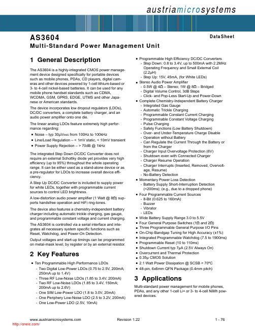
AS3604Multi-Standard Power Management Unitaustria micro systemsData Sheet1 General DescriptionThe AS3604 is a highly-integrated CMOS power manage-ment device designed specifically for portable devices such as mobile phones, PDAs, CD players, digital cam-eras and other devices powered by 1-cell lithium-based or 3- to 4-cell nickel-based batteries. It can be used for any mobile phone handset standards such as CDMA,WCDMA, GSM, GPRS, EDGE, UTMS and other Japa-nese or American standards.The device incorporates low dropout regulators (LDOs), DC/DC converters, a complete battery charger, and an audio power amplifier onto one die.The linear analog LDOs feature extremely high perfor-mance regarding:Noise – typ 30µV RMS from 100Hz to 100kHzLine/Load Regulation – < 1mV static, < 10mV transientPower Supply Rejection – > 70dB @ 1kHzThe integrated Step Down DC/DC Converter does not require an external Schottky diode yet provides very high efficiency (up to 95%) throughout the whole operating range. It can be either used as a stand-alone device or as a pre-regulator for LDOs to increase overall device effi-ciency.A Step Up DC/DC Converter is included to supply power for white LEDs, together with programmable current sources to control LED brightness.A low-distortion audio power amplifier (1 Watt @ 8Ω) sup-ports handsfree operation and HiFi ring-tones.The device also features a chemistry-independent battery charger including automatic trickle charging, gas gauge, and programmable constant voltage and current charging.The AS3604 is controlled via a serial interface and inte-grates all necessary system specific functions such as Reset, Watchdog, and Power-On Detection.Output voltages and start-up timings can be programmed on metal-mask level, by register or by an external resistor.2 Key FeaturesTen Programmable High Performance LDOs-Two Digital Low-Power LDOs (0.75 to 2.5V, 200mA; 250mA up to 1.4V)-Three RF Low-Noise LDOs (1.85 to 3.4V, 200mA) -Two RF Low-Noise LDOs (1.85 to 3.4V, 150mA; 200mA up to 2.6V)-One SIM Low-Power LDO (1.8 to 3.0V, 20mA)-One Periphery Low-Noise LDO (2.5 to 3.2V, 200mA)-One Low-Power LDO (2.5V, 10mA)Programmable High Efficiency DC/DC Converters -Step Down: 0.8 to 3.4V, up to 500mA with 2.2MHz Operating Frequency and Small External Coil (2.2µH)-Step Up: 15V, 45mA, (for White LEDs)Stereo Audio Power Amplifier-0.5W @ 4Ω – Stereo; 1W @ 8Ω – Bridged -Digital Volume Control, 3dB Steps-Click- and Pop-Less Start-Up and Power-DownComplete Chemistry-Independent Battery Charger -Integrated Gas Gauge-Automatic Trickle Charging-Programmable Constant Current Charging -Programmable Constant Voltage Charging -Pulse Charging-Safety Functions (Low Battery Shutdown)-Over- and Under-Temperature Charge Disable -Operation without Battery-Can Regulate the Current Through the Battery or from the Charger-Charger Input Overvoltage Protection (6V) -Shutdown even with Connected Charger -Charger Resume Operation-Charger Interrupts (Inserted, Removed, Overvolt-age, Resume)-No-Battery DetectionMomentary Power Loss Detection-Battery Supply Short-Interruption Detection (<200ms); (e.g., due to a dropped phone)Four Programmable Current Sources -8-Bit (0.625 to 160mA) -Buzzer -Vibrator -LEDsWide Battery Supply Range 3.0 to 5.5VFour General Purpose Switches (1Ω and 2Ω) Three Programmable General Purpose I/O Pins On-Chip Bandgap Tuning for High Accuracy (±1%) Integrated Programmable Watchdog (7.5 to 1900ms) Programmable Reset (10 to 110ms)Shutdown Current typ 7µA (2.5V Always On) Overcurrent and Thermal Protection 0.35µ CMOS Solution2.1 Watt Power Dissipation @ SCSB = 70ºC48-pin, 6x6mm QFN Package (0.4mm pitch)3 ApplicationsMulti-standard power management for mobile phones, PDAs, and any other 1-cell Li+ or 3- to 4-cell NiMh pow-ered devices.4 Block DiagramsFigure 1. AS3604 Block Diagram. Option: Audio Amplifier In Differential Mode, Step Down DC/DC Converter asPre-Regulator for Digital LDOsNote:Refer to Table 38 on page 74 for specifications of external components.2.2µHV 2_5AS3604Power ManagementUnitCharge Pump 4.74-5.25V 30mAAnalog LDO Low Noise 2.5-3.2V 200mAAnalog LDO Low Noise 1.85-3.4V 200mARF LDO Low Noise 1.85-3.4V 200mARF LDO Low Noise 1.85-3.4V 200mA RF LDO Low Noise 1.85-3.4V 200mARF LDO Low Noise 1.85-3.4V 200mAStep Up DC/DC Converter ≤15V 45mACurrent Source 4x(0.6-160mA)L122µHV BATCAPP CAPN 32C2330nFV 5_6Charge PumpC31µFC41µFC61µFC81µFC91µF C131µFBaseband Analog3.0-5.5V Baseband CoreRFTransmitterRFReceiver3.0-5.5VV BATVCO TXCOSynthesizer etc.Internal LDO 2.5V, 10mAC51µF C722µFC101µFC121µF V 2_5ON SwitchInterrupt, LCD Control, etc.Digital LDO 0.75-2.5V 250mA SIM LDO 3.0V, 20mAC111µFDigital LDO 0.75-2.5V 250mAStep Down DC/DCConverter 1.0-3.0V, 500mAC141µFC151µFFlash Memory BasebandCore (Alternate)LX 48C161µFC1810µFBaseband PeripheralsC19100nFSIM CardPORV ANA_1Digital Logic and ReferencesBoot ROMR7R PROGRAMR6220k ΩC29100nF242623RPROGRAMCREF RBIAS 10RESETR5100k ΩRESETV ANA_1I/FSerial InterfaceV 2_5 or V BAT NiMh, LiIonBattery Charger andGas GaugeR34.7k ΩR24.7k ΩC27R450m ΩC281µFLi-Ion NiMhV BATAll caps on V BAT≥10µF totalPadGND_PADC261µF R12k ΩDC Char-ger Adapter ≤15V≥8ΩLS11W Audio AmplifierC23100nF C24100nF AudioInC25100nFV BATC221µFC11µFSTEPUP36D1MBR0520White LEDs VibratorBuzzer CURR135343332CURR2CURR3CURR4VSIM46FeedbackQ1Si3441V BAT 3.0-5.5VL2VBAT_247VBUCK 40VDIG_239VDIG_141V2_522VRF_419VBAT_518VRF_317VRF_27VBAT_48VRF_19VANA_26VBAT_15VANA_14V5_61VBAT_330AOUT_L 28AIN_L 38AGND 31AIN_R 37AOUT_R29VCHARGER20VGATE21ISENSP15ISENSN 16GND_SENSE27ON 25SDI12SCLK 13SDO 11SCSB14GPIOV ANA_1 V 5_6GPIO343GPIO244GPIO145VBAT_642V BAT 3.0-5.5VFigure 2. AS3604 Block Diagram. Option: Audio Amplifier in Stereo Single-Ended Mode, Digital LDOs Separatedfrom Step Down DC/DC ConverterNote:Refer to Table 38 on page 74 for specifications of external components.NiMh, LiIonBattery Charger andFuel GaugeAS3604Power ManagementUnitCharge Pump 4.74-5.25V 30mAAnalog LDO Low Noise 2.5-3.2V 200mAAnalog LDO Low Noise 1.85-3.4V 200mARF LDO Low Noise 1.85-3.4V 200mARF LDO Low Noise 1.85-3.4V 200mA RF LDO Low Noise 1.85-3.4V 200mARF LDO Low Noise 1.85-3.4V 200mAStep Up DC/DC Converter ≤15V 45mACurrent Source 4x(0.6-160mA)L122µHV BATCAPP CAPN 32C2330nFV 5_6Charge PumpC31µFBaseband Analog3.0-5.5V Baseband CoreRFTransmitterRFReceiverGPIO3.0-5.5VV BATVCO TXCOSynthesizer etc.Internal LDO2.5V 10mAV 2_5ON SwitchInterrupt, LCD Control, etc.V ANA_1 V 5_6Digital LDO 0.75-2.5V 250mA SIM LDO 3.0V, 20mADigital LDO 0.75-2.5V 250mAStep Down DC/DCConverter 1.0-3.0V, 500mAFlash Memory 3.0-5.5VSIM CardPORV ANA_1Digital Logic and ReferencesBoot ROM10RESETR5100k ΩRESETV ANA_1I/FSerial InterfaceV 2_5 or V BATR34.7k ΩR24.7k ΩC27R450m ΩC281µFLi-Ion NiMhV BATAll caps on V BAT≥10µF totalC261µF R12k ΩDC Char-ger Adapter ≤15V≥4ΩLS21W Audio AmplifierC20≥100µF C21≥100µFIN _LV BATC221µFC11µFSTEPUP36D1MBR0520White LEDs Vibrator Buzzer CURR135343332CURR2CURR3CURR4V 2_51.0-5.5V FeedbackQ1Si3441≥4ΩLS3IN _RC23100nFC25100nF Baseband Core(Alternative)C24100nFR7R PROGRAMR6220k ΩC29100nF242623RPROGRAM CREF RBIASPadGND_PADC41µFC51µF C101µFC91µF C111µFC121µF C131µFC19100nFC301µFC722µFC141µFVBAT_330AOUT_L28AIN_L 38AGND 31AIN_R37AOUT_R29VCHARGER20VGATE21ISENSP15ISENSN 16GND_SENSE27ON 25SDI12SCLK 13SDO 11SCSB14LX 48VSIM46VBAT_247VBUCK 40VDIG_239VDIG_141GPIO343GPIO244GPIO145V2_522VRF_419VBAT_518VRF_317VRF_27VBAT_48VRF_19VANA_26VBAT_15VANA_14V5_61C61µFC81µFC151µFVBAT_642V BAT 3.0-5.5V2.2µHC161µFC1810µF Baseband PeripheralsL2Content1 General Description (1)2 Key Features (1)3 Applications (1)4 Block Diagrams (2)5 Absolute Maximum Ratings (Non-Operating) (6)5.1 Operating Conditions (6)6 Detailed Functional Descriptions (7)6.1 Battery Charger Controller (7)6.2 Step Down DC/DC Converter (24)6.3 Low Dropout Regulators (30)6.4 Charge Pump (41)6.5 Step Up DC/DC Converter (42)6.6 General Purpose Input/Output (44)6.7 Current Sinks (50)6.8 Audio Amplifier (53)7 System Supervisory Functions (56)7.1 Reset (56)7.2 Startup (58)7.3 Protection Functions (59)7.4 Watchdog Block (60)7.5 Internal Reference Circuits (61)7.6 Low Power Mode (63)7.7 Boot Sequence Detection (63)7.8 Serial Interface (64)8 Register Map (68)9 Pinout and Packaging (70)9.1 Pin Descriptions (70)9.2 Package Drawings and Markings (72)10 External Parts List (74)11 Ordering Information (75)Revision HistoryRevision Date Owner Description1.023 June 2006ptr - Initial release.1.1 3 March 2007ptr- Updated ambient temperature range.1.11 4 Dec 2008pkm- Updated internal LDO supply description1.28 Apr 2009pkm- Updated ordering info for AS3604B chip version1.2115 Mai 2009pkm - Updated abs. max ratings and stand-by current, deleted errata1.2221 Aug 2009pkm- Updated operating current, SNR and VCHOV5 Absolute Maximum Ratings (Non-Operating)Stresses beyond the absolute maximum ratings may cause permanent damage to the AS3604. These are stress rat-ings only. Functional operation of the device at these or beyond those in Operating Conditions is not implied. Caution:Exposure to absolute maximum rating conditions may affect device reliability.5.1 Operating ConditionsTable 1. Absolute Maximum Ratings Symbol Parameter Min Max Unit NotesV IN_HVHigh Voltage Pins-0.318.0VApplicable for high voltage pins: VCHARGER, VGATE, and STEPUP V IN_MV 5V Pins -0.37.0VApplicable for pins 5V pins:VBAT_1 - VBAT_6, V5_6, VBUCK, GPIO1 - GPIO3, CURR1 - CURR4, AIN_L, AIN_R, AOUT_L, AOUT_R, VRF_1 - VRF_4 (when not in LDO-mode), ON, and LXV IN_LV 3.3V Pins -0.3 5.0VApplicable for 3.3V pins:RESET, SCSB, SCLK, SDI, SDO, VANA_1, VANA_2, VSIM, VDIG_1, VDIG_2, CAPN, AGND, ISENSP, ISENSN, V2_5, CREF, RBIAS, and RPROGRAM I IN Input Pin Current -25+25mA At 25ºC Norm: JEDEC 17T strg Storage Temperature Range-55125ºC Humidity585%Non-condensingV ESD Electrostatic Discharge -10001000V Norm: MIL 883 E Method 3015; ±1000V.P T Total Power Dissipation 2.1W T AMB = 70ºCT maxPeak Reflow SolderingTemperature260ºCT = 20 to 40s, according to the IPC/JEDEC J-STD 020C.Table 2. Operating Conditions Symbol Parameter Min TypMax Unit NotesV HV High Voltage 0.015.0V Pins VCHARGER, VGATE and STEPUP V BAT Battery Voltage 3.0 3.6 5.5V For pins VBAT_1 - VBAT_6. Duringstartup from ext. battery charger adapter, the battery voltage can be below 3.0V.V ANA_1Periphery Supply Voltage (for RESET and SPI pins) 2.5Boot ROM 3.2V Internally generated from V ANA_1.V ON Activation voltage for ON pin1.75V 2_5V BAT V V 2_5Voltage on Pin V2_52.4 2.5 2.6V Internally generated.V 5_6Output Voltage of Charge Pump5.0 5.2 5.6V 2 x V ANA_1T AMB Ambient Temperature -402585ºC I BATOperating Current 195260µANormal operating current. With bitlow_power_on (page 62) = 0; only V ANA_1 active, no additional external loads.I LOWPOWER Low-Power Mode CurrentConsumption 110µAWith bit low_power_on (page 62) = 1; only V ANA_1 active, no additional external loads.I POWEROFF Power-Off Mode CurrentConsumption1320µAWith bit power_off (page 57) = 1; only V2_5 is active in power off mode.not tested, guaranteed by design6 Detailed Functional Descriptions6.1 Battery Charger ControllerThe AS3604 can serve as a standalone Battery Charger Controller supporting rechargeable lithium-ion (Li+), lithium-polymer (LiPo) and 3- or 4-cell nickel metal-hydride (NiMh) batteries.The main features of the Battery Charger Controller are:Constant Voltage Charge Mode – Described on page 9 Pulse Charge Mode – Described on page 11Battery Presence Detection – Described on page 14 Operation Without Battery – Described on page 14 Charge Controller Bypass – Described on page 14Overvoltage and Undervoltage Supervision – Described on page 15Figure 3. Battery Charger Controller Block DiagramTable 3. Battery Charger Controller ComponentsSymbol Parameter ValueNotesM CHG P-Channel MOSFET Si3441BDV, Si8401DB or similar The maximum power dissipation of thistransistor is not limited by the AS3604.R PUP Pull-Up Resistor 2K Ω ± 5%R SENSE Current Sense Resistor50m Ω ± 1%, 125mW for I VBAT,DC < 1.5Ae.g. Vishay Dale WSL0805R FILT1,2Filter Resistor 47K Ω ± 1%Can be omitted if Gas Gauge functionalityis not used (R FILT1,2 = 0Ω)C FILT Filter Capacitor 100nF ± 20%, X5R or X7R Dielectric C CHRG Bypass Capacitor on pin VCHARGER 1µF ± 20%, X5R or X7R DielectricC BATMinimum Total CapacitanceParallel to Battery10µF C BATVCHARGERR SENSE AS3604Battery Charger ControllerVGATEVBAT_5ISENSPISENSNVSSR PUPM CHGR FILT1BATTGND_PCBV BATChargerC CHRGC FILTR FILT26.1.1 Low-Current Trickle Charge ModeLow-Current Trickle Charge mode is initiated when an external battery charger has been detected, bit chDet (page 19)= 1, and the battery voltage is below the VUVLO threshold; bits ChAct (page 19) and Trickle (page 19) will be set. In Trickle Charge mode the charge current will be limited to the value specified by Trickle Current (page 21) to prevent undue stress on either the battery or the Battery Charger in case of deeply discharged batteries.Once VUVLO has been exceeded, the Battery Charger will terminate Trickle Charge mode (charger must not be dis-abled between trickle and constant current (fast) charging), reset bits ChAct and Trickle , and switch on the device.The trickle charge is terminated in any case after approximately 60 minutes (as it is assumed that the battery is dam-aged in this case)6.1.2 Constant Current Charge ModeConstant Current mode is initiated by setting bit ChEn (page 20) and resetting bit Fast (page 20). Bit ChAct (page 19) is set automatically when the Battery Charger starts. Charge current will be limited to the value specified by bit Constant Current (page 21) by the Battery Charger Controller.6.1.3 Charging Nickel-based BatteriesFor nickel-based batteries (NiMh), BatType (page 20) must be 1 (see Figure 4 on page 9). The endpoint detection (ΔV/Δt) must be performed by the host controller. It must turn off the charger duly to avoid overcharging. In any case, when the battery voltage exceeds the charge termination threshold (typ. 5.5V), the charger will be turned off and bit EOC (page 20) will be set.6.1.4 Charging Lithium-based BatteriesFor lithium-based batteries (Lithium-Ion, Lithium-Polymer), BatType (page 20) must be 0. Additionally, bit Li4v2(page 20) can select between coke- and graphite-anode, setting different charge termination thresholds (typ. 4.1 or 4.2V). The charger is designed to charge 1-cell lithium-based batteries independently, using Trickle Charge, Constant Current, Constant Voltage, or Pulse Charge modes.When the battery voltage exceeds the charge termination threshold during Constant Current mode, it automatically continues charging with either Constant Voltage mode, bit Pulse (page 20), or Pulse Charge mode, Pulse , and termi-nates when the end-of-charge conditions are met (see Figure 5 on page 11 and Figure 6 on page 13).Table 4. Battery Charger Controller Parameters Symbol ParameterMin Typ Max Unit NotesV CHDET Charger Detection Threshold. VCHARGER - VBAT_5: Charger On 5075105mV Hysteresis = (V CHDET - V CHMIN )< 40mVV CHMIN Charger Detection Threshold. VCHARGER - VBAT_5: Charger Off52035mV V CHREG Bootstrap Regulator Voltage 2.4 2.52.6V VCHARGER > 5VV CHOVH VCHARGER Overvoltage Detection6.26.456,71VMonitor voltage on VCHARGER and disable charging if this voltage is exceeded.V CHOV 5,81 6.056,29V UVLO Undervoltage Lockout Threshold 3.1V V BAT rising 2.8V BAT falling V OVLOOvervoltage Lockout Threshold5.5VV BAT rising 5.4V BAT fallingV CHOFF Charge Termination Threshold4.14 4.20 4.26VLi+ Battery: BatType (page 20) = 0, Li4v2(page 20) = 14.05 4.1 4.15Li+ Battery: BatType = 0, Li4v2 = 0.From -5 to +50ºC 5.445.55.6NiMh Battery: BatType = 1V NOBATDET No-Battery Detection Threshold andCharger Resume Detection Threshold3.644VDisOWB (page 21) = 0Figure 4. Startup and Constant Current Charging of Nickel-based Batteries6.1.5 Fast Charge ModeAs an alternative to Constant Current mode, Fast Charge mode may be selected. The charge current will not be con-trolled in this mode and is only limited by the external battery charger adapter.Fast Charge mode is initiated by setting bits ChEn (page 20) and Fast (page 20). Bit ChAct (page 19) is set when the Bat-tery Charger has started.End of ChargeIn Fast Charge mode, the same charge termination thresholds apply as for Constant Current mode. Additionally,depending on bit Fast (page 20), the current during pulse charging is either the selected constant current or maximum. Charging will resume if the battery voltage drops below V NOBATDET .6.1.6 Constant Voltage Charge ModeConstant Voltage mode is initiated and bit CVM (page 19) will be set when threshold V CHOFF (page 8) has been exceeded for the first time (no debounce filter) and bit Pulse (page 20) is not set.External Charger at Pin V CHARGERPrinciple Only. Not To Scale.V BATI CHARGETrickle CurrentConstant Current or Fast CurrentV UVLO 3.1VV CHDET0VPower up LDOs = Boot ROMLDO Voltages Serial Communication PossibleResetRegister Settings (Write)ChEn µC: ActivateCharger μC: Turn Off ChargerPulseChDet Register Settings (Read)Trickle ChAct CVM EOCTrickle Charge ModePower Up; No ChargeConstant Current ModeBit EOC is only set when V CHOFF is exceededt = 06-11mst10-110msΔV/ΔI Detection by External ADCV CHOFF = 5.5V (BatType = 1)CC Charging Terminates Immediately when V CHOFF is exceeded BatType µC: Select Battery TypeThe charge controller will regulate the battery voltage to a value set by bit Li4v2(page 20). To enable operation of the device without a battery connected to the system it is necessary that the charger is not disabled between the moment when the V CHOFF threshold is exceeded for the first time and the beginning of constant voltage charge mode.During Constant Voltage mode, the charge current will decrease and eventually drop below the value set by Trickle Current(page 21). If the measured charge current is less than or equal to Trickle Current, charging is terminated and bit EOC is set. Charging will resume if the battery voltage drops below V NOBATDET.If the battery has been removed during constant voltage charging the EOC condition and the no battery condition will probably conflict. To be able to properly detect the EOC state the EOC condition has to be dominant over the no battery condition.If the battery voltage (VBAT_5) drops below V NOBATDETECT (page 8) (signal resume starts pulsing), e.g. if the bat-tery is removed after charging is finished, EOC(page 20) will be cleared (after debounce time) and the battery char-ger controller will resume in constant voltage mode to enable operation of the device without battery. This only works if bit CVM(page 19) remains set when bit EOC is set, otherwise the comparators that are required for operation without battery are gated.Three scenarios are possible at this point:1. If a battery is connected the charge current will now be high and charging will return to constant current charg-ing.2. No battery is connected and no current will flow through the sense resistor. Now the no battery condition isdetected properly.3. The battery was connected and is disconnected. No current will flow through the sense resistor and the no bat-tery condition is detected properly.In summary: When charging is resumed after an EOC state either a (dis)charge current will be measured and the charge controller will return to constant current mode or no current will be measured and a “no battery”condition is indicated. To be able to handle supply voltage spikes caused by e.g. battery bouncing when the system is heavily shaken the V NOBATDETECT detection has to be debounced for 1 current measurement cycle before EOC is cleared. After the debounce time is over additional pulses must occur during the next current measurement cycle to clear EOC.The no battery status is indicated with bit NoBat(page 20).If the battery is replaced after charging is finished and the charge current exceeds the value set by ConstantCurrent(page 21), the charge controller will clear bit CVM and return to Constant Current or Fast Charge mode, depend-ing on bit Fast(page 20).Notes:1. Bit CVM will be ambiguous if bit Fast is set.2. EOC will only be entered if bit AutoChgTerm(page 21) is set (default = 0).分销商库存信息:AMSAS3604-ZQFT AS3604-ZQFU。
ZL6105中文资料(Intersil)中文数据手册「EasyDatasheet - 矽搜」
该ZL6105使用I
2C / SMBus接口PMBus协议
与主机控制器和数字直流总线齐尔科尔实验室设备之间通信
通信.
该ZL6105是引脚对引脚与ZL2008兼容.该
POLA V OUT 表补偿表已被删除.
一种新单电阻V
OUT 表和自动补偿
特征已被添加.
芯片中文手册,看全文,戳
与驱动器和自动数字DC / DC控制器
赔偿金
ZL6105
该ZL6105是集成数字电源控制器 MOSFET驱动器.自动补偿,无需手动补偿设计工作.自适 应性能优化算法,提高电源转换效率.
Zilker Labs数字直流技术使混合动力转换性能和电源管理 功能.
所述ZL6105设计是灵活产品木为直流电力,并可以很容易地适 应设计从在3.3V操作到一个多相电流共享供给从12V输入 操作单相电源.
图3:12V至1.8V / 16A应用电路
芯片中文手册,看全文,戳
ZL6105
Input Voltage Bus
VR
Power Management
NVM
BST
MOSFET
SYNC GEN
Digital Compensator
D-PWM
Drivers SW
V
PLL ADC
-
+
ADC
•电压跟踪,排序和裕度
•电压,电流和温度监测
• I 2C / SMBus接口,兼容PMBus
•输出电压和电流防护护
•内部非易失性存储器(NVM)
应用
•服务器/存储设备 •电信/数据通信设备 •电源模块
芯片中文手册,看全文,戳
2N2905A;中文规格书,Datasheet资料
2N2905A 2N2907ASMALL SIGNAL PNP TRANSISTORSDESCRIPTION The 2N2905A and 2N2907A are silicon Planar Epitaxial PNP transistors in Jedec TO-39 (for 2N2905A) and in Jedec TO-18 (for 2N2907A)metal case. They are designed for high speed saturated switching and general purpose applications.February 2003ABSOLUTE MAXIMUM RATINGS®1/7THERMAL DATAELECTRICAL CHARACTERISTICS (T case = 25 oC unless otherwise specified)** See test circuit2N2905A/2N2907ANormalized DC Current Gain.Collector Emitter Saturation Voltage.Collector Base and Emitter-base capacitances.Switching Characteristics.2N2905A/2N2907A2N2905A/2N2907A.Test Circuit for t on, t r, t d ArrayTest Circuit for t off, t o, t f.2N2905A/2N2907A2N2905A/2N2907AInformation furnished is believed to be accurate and reliable. However, STMicroelectronics assumes no responsibility for the consequences of use of such information nor for any infringement of patents or other rights of third parties which may result from its use. No license is granted by implication or otherwise under any patent or patent rights of STMicroelectronics. Specification mentioned in this publication are subject to change without notice. This publication supersedes and replaces all information previously supplied. STMicroelectronics products are not authorized for use as critical components in life support devices or systems without express written approval of STMicroelectronics.The ST logo is a trademark of STMicroelectronics © 2003 STMicroelectronics – Printed in Italy – All Rights ReservedSTMicroelectronics GROUP OF COMPANIESAustralia - Brazil - Canada - China - Finland - France - Germany - Hong Kong - India - Israel - Italy - Japan - Malaysia - Malta - Morocco - Singapore - Spain - Sweden - Switzerland - United Kingdom - United States.2N2905A/2N2907A分销商库存信息: STM2N2905A。
09-52-3073;中文规格书,Datasheet资料

SDA-2145-002
/
MMSTROH
MKIPPER
FSMITH
TEMPLATE FILENAME: PRODUCT_SPEC[SIZE_A](V.1).DOC
分销商库存信息:
MOLEX 09-52-3073
NONE TRAY PACKAGING: PK-2145-001 A-2145-CANA208 Material No 09-62-3023 09-62-3033 09-62-3043 09-62-3053 09-62-3063 09-62-3073 09-62-3083 09-62-3093 09-62-3103 09-62-3113 09-62-3123 09-62-3133 09-62-3143 09-62-3153
Ref Ckt 2 3 4 5 6 7 8 9 10 11 12 13 14 15
NONE TRAY PACKAGING: PK-2145-001 A-2145-CANB102 Material No 09-62-6025 09-62-6035 09-62-6045 09-62-6055 09-62-6065 09-62-6075 09-62-6085 09-62-6095 09-62-6105 09-62-6115 09-62-6125 09-62-6135 09-62-6145 09-62-6155 REV:
Ref Ckt 2 3 4 5 6 7 8 9 10 11 12 13 14 15
NONE TRAY PACKAGING: PK-2145-001 A-2145-CANA102 Material No 09-52-1023 09-52-1033 09-52-1043 09-52-1053 09-52-1063 09-52-1073 09-52-1083 09-52-1093 09-52-1103 09-52-1113 09-52-1123 09-52-1133 09-52-1143 09-52-1153 REV:
LSZ1R;LSZ1E;LSZ1V;LSZ1D;LSZ1W;中文规格书,Datasheet资料

If you need detailed product information, or help choosing the right product for your application, see our Interactive Catalog . Use the Interactive Catalog to access the most complete and up-to-date information available.The Interactive Catalog provides an extensive collection of product specifications, application data, and technical literature that can be searched based on criteria you select.This PDF catalog information was published in November 2000.Sensing and Control Honeywell Inc.11 West Spring Street Freeport, IL 61032/sensingSensing and ControlInteractive Catalog...Click this icon to try the Interactive Catalog.Interactive Catalog Supplements Catalog PDFsHoneywell ɀ Sensing and Control ɀ1-800-537-6945 USA ɀ⍣1-815-235-6847 International ɀ1-800-737-3360 Canada Delrin Coil Rod Spring LSZ4009LSZ4014inch long. For 7MICRO SWITCH conduit sealing packets can be used with limit or enclosed switches.This includes the HDLS, Compact LS, ML,E6, V6, BAF1or OP series switches.The conduit sealing packets are not suitablefor use with explosion-proof switches.This tool kit is used if readjustment of switch-es is necessary when heads and/or contactdetermine replacement parts catalog listing. The list-ings with -7A, -7M, -7N, -8A, -8B and -8C are complete catalog listings.B. Example LSZ1AB. For fluorocarbon seal replacement heads add C. Example LSZ1AC.A50Honeywellɀ Sensing and Controlɀ1-800-537-6945 USAɀ⍣1-815-235-6847 Internationalɀ1-800-737-3360 Canadadetermine replacement parts catalog listing. The list-ings with -7A, -7M, -7N, -8A, -8B and -8C are complete catalog listings.**Includes actuator B. Example LSZ1AB. For fluorocarbon seal replacement heads add C. Example LSZ1AC.Honeywellɀ Sensing and Controlɀ1-800-537-6945 USAɀ⍣1-815-235-6847 Internationalɀ1-800-737-3360 Canada A51determine replacement parts catalog listing. The list-ings with -7A, -7M, -7N, -8A, -8B and -8C are complete catalog listings.tors add B between the fifth and sixth characters. Example: LSZ1K B HA. For fluorocarbon seals add C. Example LSZ1K C HA.A52Honeywellɀ Sensing and Controlɀ1-800-537-6945 USAɀ⍣1-815-235-6847 Internationalɀ1-800-737-3360 Canadadetermine replacement parts catalog listing. The list-ings with -7A, -7M, -7N, -8A, -8B and -8C are complete catalog listings.Example LSZ1AB. For fluorocarbon seal replace-ment heads add C. Example LSZ1AC.Honeywellɀ Sensing and Controlɀ1-800-537-6945 USAɀ⍣1-815-235-6847 Internationalɀ1-800-737-3360 Canada A53*Only partial listings are shown and necessary to determine replacement parts catalog listing. The list-ings with -7A, -7M, -7N, -8A, -8B and -8C are complete catalog listings.Note: Complete units consist of Columns 1and 2.‡For low temperature replacement head and actua-tors add B between the fifth and sixth characters.Example LSZ1K B HA. For fluorocarbon seals add C.Example LSZ1K C HA.A54HoneywellɀSensing and Controlɀ1-800-537-6945 USAɀ⍣1-815-235-6847 Internationalɀ1-800-737-3360 CanadaHoneywell ɀSensing and Control ɀ1-800-537-6945 USA ɀ⍣1-815-235-6847 International ɀ1-800-737-3360 Canada A55分销商库存信息:HONEYWELLLSZ1R LSZ1E LSZ1V LSZ1D LSZ1W LSZ1F LSZ3A LSZ1A LSZ1KHA LSZ1JGM LSZ1C LSZ1G。
LT6105中文资料
n n n n n n n n n n
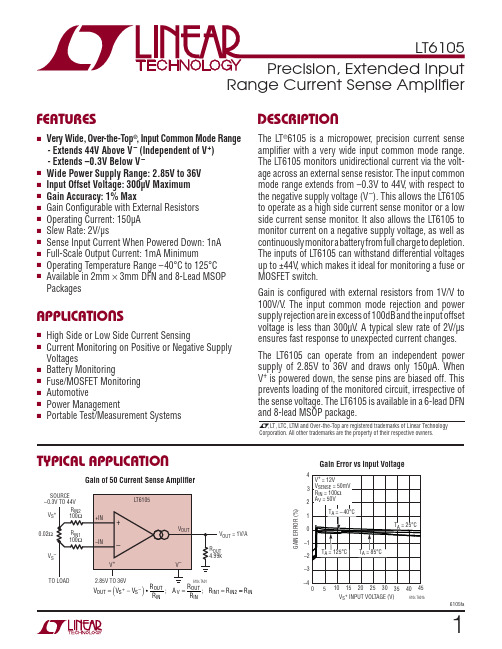
Very Wide, Over-the-Top®, Input Common Mode Range - Extends 44V Above V – (Independent of V +) - Extends –0.3V Below V – Wide Power Supply Range: 2.85V to 36V Input Offset Voltage: 300μV Maximum Gain Accuracy: 1% Max Gain Configurable with External Resistors Operating Current: 150μA Slew Rate: 2V/μs Sense Input Current When Powered Down: 1nA Full-Scale Output Current: 1mA Minimum Operating Temperature Range –40°C to 125°C Available in 2mm × 3mm DFN and 8-Lead MSOP Packages
元器件交易网
LT6105 ABSOLUTE MAXIMUM RATINGS
(Notes 1, 2)
Differential Input Voltage (+IN – –IN) .....................±44V Input Voltage V(+IN, –IN) to V – ................ –9.5V to 44V Total V+ Supply Voltage from V – ...............................36V Output Voltage ......................................V – to (V – + 36V) Output Short-Circuit Duration (Note 3) ............ Indefinite Operating Temperature Range (Note 4) LT6105C...............................................–40°C to 85°C LT6105I ................................................–40°C to 85°C LT6105H ............................................–40°C to 125°C
A8300_模块硬件接口手册_V0.1 周立功_龙尚_2G模块
1230;1495;5070;5071;5072;中文规格书,Datasheet资料

1CAT.NO.1236.025SQUARE WIRE WRAP PINSCONTACT PINS (SEAMLESS)Completely burr free straight to within .003(.08)per inch.Conical ends of square-wire with smooth blend-in radius on corners assures ease of insertion with minimum damage to pre-plated PCB holes.Pins can be staked to .062(1.57)and .093(2.36)thick boards.“FLEA”CLIP“IMP”TERMINAL“MICRO”TERMINALFor subminiature applications where conventional terminals are too large or too costly.Ideal for quick repairs of printed circuitry.Simply insert wire through hole and it is held firmly by spring action assuring continued postive contact.•Quick and Easy to Install •For Production or Prototype•Postive Locking In-Hole •No Staking Required •Holds .010(.25)to .050(1.27)Diameter WireThese terminals are often used for transistor and Bi-Pin lamp sockets.Terminals snap into place and are firmly held without the need of staking.Wire leads can be inserted from either end.Terminals 1236and 1237have tapered socket spring forming that will hold multiple leads in place.Terminals are pre-tinned for easy soldering.CAT.NO.1237CAT.NO.1238Easily press-fit into a .042(1.07)diameter hole may be flared for permanent installation.Ideally designed for use in circuitry to support components when space is at a premium.CAT.NO.1495Excellent for point to point or feed thru wiring.Slot is serrated to grip component leads.Multiple connections are made quick and easy.CLAMP TERMINALCAT.NO.1499FTCAT.NO.1500Terminal for production or prototype use.Holds as many as 7leads without soldering,by spring action.CAT.NO.1498CPAAB.125 [3.2].034[.86].025[.64]60°L.010[.25].003R .[.08 R ].812[20.6].260[6.6].032[0.81].085[2.16].085[2.16].312[7.9].062[1.57].234 [6.0]REF..040[1.02]DIA..094[2.39]CAT.NO.A B 1223.093(2.36).293(7.4)1224.093(2.36).357(9.1)1226.093(2.36).437(11.1)1200.125(3.18).379(9.6)1210.125(3.18).566(14.4)1230.156(3.96).379(9.6)1231.156(3.96).566(14.4)MATERIAL:Phosphor Bronze,Tin PlateMATERIAL:Brass,Nickel Plate.375[9.6].187[4.8].053 [1.34].053[1.35]REF..058[1.48].052 [1.32].064 [1.7].078 [1.98]REF..030[.76].130 [3.3].045[1.14]DIA..237[6.0].437[11.1].063 [1.6] REF..046 [1.17].100 [2.6].078 [1.98].359[9.1].167[4.3].030 [.76].034 [.86].031 [.79]DIA..018 [.46]DIA..065 [1.65]DIA..080 [2.03]DIA. FLANGE.050 [1.27]I.DIA..219[5.6].328[8.4].047 [1.19].188[4.8].469[11.9].219[5.6].080 [2.03]DIA. FLANGE.050[1.27]I.DIA..065[1.65]DIA..065[1.65]DIA..080[2.03]DIA.FLANGE.050[1.27]I.DIA..219[5.6].046[1.17]DIA.FLARE.469[11.9].188[4.8]Insertion Tool:CAT.NO.1323Insertion Tool:CAT.NO.1322Insertion Tool:CAT.NO.1322Insertion Tool:CAT.NO.1322Mtg.Hole .062(1.57)Mtg.Hole .062(1.57)Mtg.Hole .093(2.36)MATERIAL:.006(.15)Matte Tin,Brass.Pre-TinnedMATERIAL:.008(.20)Matte Tin,Beryllium Copper,Tin PlateMATERIAL:.008(.20)Matte Tin,Beryllium Copper,Tin PlateMATERIAL:.015(.38)Matte Tin,Spring Steel,Tin PlateMATERIAL:.008(.20)Matte Tin,Beryllium Copper,Tin Plate MATERIAL:.006(.15)Matte Tin,Brass.Pre-TinnedMATERIAL:.006(.15)Matte Tin,Brass.Pre-Tinned.062(1.57)—.067(1.70)Mounting HolesTel (718)956-8900•Fax (718)956-9040(800)221-5510•kec@31-0720th Road –Astoria,NY 11105-2017RoHS COMPLIANT ~ISO 9001CERTIFIED®For Arbor Press:CAT.NO.TL-11;For Hand Tool:CAT.NO.1214INSERTION TOOLCAT.L CAT.L NO.Length NO.Length 5070.400(10.2)5077.642(16.3)5071.440(11.2)5078.675(17.1)5072.515(13.1)5079.720(18.3)5073.535(13.6)5080.850(21.6)5074.600(15.2)5081.916(23.3)5075.615(15.6)5082.995(25.3)5076.625(15.9)5083 1.13(28.7)分销商库存信息:KEYSTONE-ELECTRONICS123014955070 507150725073 507450755076 507750785079 508050825083 5081。
遥控器资料查询

M50431-101SP TMP47C433AN M50453/431-101SP M50453/431-101SP M50453/431-101SP PCA84C440/504/640/641 PCA84C440/504/640/641 PCA84C440/504/640/641 TMP47C432/433/434AN TMP47C432/433/434AN M50436-560SP PCA84C440/504/640/641 M34300N4-012 TMP47C432/433/434AN M50436-560SP M50453/431-101SP TMP47C432/433/434AN M34300N4-012 M50453/431-101SP
127
长虹
K8B
TC901C K9D
TC9012 SAA3010T SAA3010
131 132 133 134 135 136 137 138 139 140 141 142 143 144 145 146 147 148 149 150 151 152 153 154 155 156 157 158 159 160 161 162 163 164 165 166 167 168 169 170 171 172 173 174 175 176
遥控器IC型号 遥控器 型号 20142 D6600 D6600 D6600 D6600 D6600
电视机CPU型号 型号 电视机
TC-9028-021 SAA3010 SAA3010 SAA3010 SAA3010
LUKS-5140-M2
SAA3010 SAA3010
TC9012-011
TC9012-011
TMP47C433AN TMP47C433AN TMP47C433AN-3849 TMP47C433AN TMP47C433AN TMP47C433AN TMP47C433AN TMP47C433AN M50436-560SP M50436-560SP PCM84C640/CH05001
BP6A-L;中文规格书,Datasheet资料

BP6A – L-Series IPM Interface Circuit Reference DesignDescription: The BP6A is a complete isolated interface circuit for high power six pack L-Series IPMs. This circuit provides opto-coupled isolation for control signals and isolated power supplies for the IPM’s built-in gate drive and protection circuits. The isolated interface helps to simplify prototype development and minimize design time by allowing direct connection of the IPM to logic level control circuits.Features: • Complete three-phase isolated interface circuit with fault feedback • 2500VRMS isolation for control power and signals• Standard AMP MTA .100” Input Signal and ControlPower Connectors• Operates from a single 24VDC supply• Compact Size 3.2” x 5.5” (80mm x 140mm)Ordering Information: BP6A-L is a kit containing a bare PCB and six VLA106-24151 DC to DC converters(For use with L-Series IPMs in package D)BP6A is a bare PCB only.Note: User must supply Opto-Couplers and passive components to fully populate the BP6A (See Table 2)Applications:BP6A is designed for use with Powerex L-Series sixpack IPMs: 450A-600A 600V and 200A-450A 1200V.¾ Use Powerex VLA106-24151 DC to DCconverter for isolated control power. SeeTable 1 for requirements.Caution: Verify PCB Orientation Before Applying PowerPackage APackage BPackage CPackage D only four isolated supplies are required. Interface circuit details for分销商库存信息: POWEREXBP6A-L。
ORD228VL-1520;ORD228VL-1015;ORD228VL-2030;中文规格书,Datasheet资料

ORD228VL
Miniature High-performance
J2R0015-41-31
n (&/&3"-%&4$3*15*0/ The ORD228VL is a small single-contact reed switch designed for general control of medium
1*
%0
NW
$3
Before test
(-55ˆ to 125 ˆ) After tes t
Contact resistance
Pull-in Value • Drop-out Value
"5
1*
%0
NW
$3
-10ˆ to 65 ˆ 80% to 98%
Before test
After test
(5) Low temperature storage test
Pull-in Value • Drop-out Value
"5
1*
%0
FL75L05 A;中文规格书,Datasheet资料
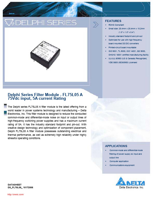
FL75R10A Filter Module75Vdc Input Maximum, 10A MaximumFEATURESROHS CompliantSmall size: 25.4mm x 25.4mm x 10.2mm(1.0” x 1.0” x 0.4”)Industry standard footprint and pin-outOptimized for use with high frequency Array board mounted DC/DC convertersPrinted-circuit board mountableISO 9001, TL 9000, ISO 14001, QS 9000,OHSAS 18001 certified manufacturing facilityUL/cUL 60950 (US & Canada) Recognized,VDE 0805 (IEC60950) LicensedDelphi Series Filter Module -FL75L05 A75Vdc input, 5A current RatingThe Delphi series FL75L05 A filter module is the latest offering from aworld leader in power systems technology and manufacturing – DeltaElectronics, Inc. This filter module is designed to reduce the conductedcommon-mode and differential-mode noise on input or output lines ofhigh-frequency switching power supplies and has a maximum currentrating of 5A. It has the industry standard footprint and pin-out. Withcreative design technology and optimization of component placement,Delphi FL75L05 A filter module possesses outstanding electrical andthermal performance, as well as extremely high reliability under highlystressful operating conditions.APPLICATIONSCommon-mode and differential-modefiltering of power supply dc input andoutput lineComputer applicationCommunications equipmentSPECIFICATIONSGENERAL SPECIFICATIONSOUTPUT SPECIFICATIONSInput voltage, continuous Typical 0~75V Output current Ta=75°C, no airflow 5A Input voltage, transient Typical 100V Output current Ta=85°C, no airflow 4A Operation case temperature Typical-40¢ ~ 120¢ Common-modeInsertionLoss50£circuit, 500 kHz (Typ)43dB Storage temperature Typical -55¢ ~ 125¢ Differential-modeInsertionLoss50£circuit, 500 kHz (Typ)45dB Size (1.0”. x 1.0”x 0.4”). 25.4 x 25.4 x 10.2 mmELECTRICAL CHARACTERISTICS CURVESFigure 1:Typical common-mode insertion loss in a 50£circuit Figure 2: Typical differential-mode insertion loss in a 50£circuitInternal SchematicsFigure 3: Internal schematicsTHERMAL CONSIDERATIONSusually the dominant mode of heat transfer.tunnel.Thermal Testing Setupthe power modules are mounted.The following figure shows the wind tunnelcharacterization setup. The filter module is mounted onNote: Wind Tunnel Test Setup Figure Dimensions are in millimeters and (Inches)Figure 4: Wind tunnel test setup figure dimensions are inmillimeters and (inches).The allowed maximum hot spot temperature is defined at 120FL75L05 (Standard) Output Current vs. Ambient Temperature and Air Velocity5055606570758085Ambient Temperature (¢)Figure 6: Output Current vs. Ambient Temperature and AirVelocity @ Vin = 48V (Either Orientation)APPLICATIONNote: C2 through C5 can be 0.01£g F to o.1£g F. Select the voltage rating to meet input-to-output isolation requirements. C1 should be the recommended value indicated in the power module data sheet.Figure 7. Recommended schematic when used as the input filter to a high-frequency dc-to-dc converterNote: Vdc input(+) and Vdc input(-) planes should overlay each other, as should the Vi(+) and Vi(-) planes, as should the Vout(+) and Vout(-) planes. Avoid routing signals or planes under the power module or the filter module. Ensure all connections are low impedance.Figure 8. Recommended layout when used as the input filter to a high-frequency dc-to-dc converterAPPLICATION (Continued)Note: : C2 through C5 and C6 through C9 can be 0.01£g F to o.1£g F. Select the voltage rating to meet input-to-output isolation requirements. C1 should be the recommended value indicated in the power module datasheet.Figure 9. Recommended schematic of filter module with two power modulesFigure 10 shows the experimental result obtained by using this filter module, together with the recommended external components shown in Figures 5 and 6. The Q48SR3R335NR module is one of the Delphi series quarter brick 3.3V, 35A DCDC converters. Measured noise is greatly dependent on layout, grounding, cable orientation, and load characteristics and the variation is possible from various application conditions.Figure 10.Q48SR3R335NR A conducted noise with FL75L05 input filterMECHANICAL DRAWINGTop View Side View Bottom ViewDimensions are in millimeter and (inches).Tolerances : x.xx 0.5 mm (0.02 in), x.xxx 0.25 mm (0.010 in)RECOMMENDED HOLE PATTERNDimensions are in millimeter and (inches).Tolerances : x.xx 0.5 mm (0.02 in), x.xxx 0.25 mm (0.010 in)PART NUMBERING SYSTEMFL 75L05 AProduct Family Input Voltage Product Series Output Current Space Option CodeFL- EMI Filter 75- 0 ~ 75V L – Industry standard05 - 5A A - Standard FunctionsMODEL LISTModule Name Input Voltage (max.) Current Rating (max.)Size (metric) Size (English unit) FL75L05 A 75V 5A 25.4 x 25.4 x 10.2 mm 1.0 in. x 1.0 in. x 0.4 in.FL75L10 A 75V 10A 50.8 x 27.9 x 12.5 mm 2.0 in. x 1.1 in. x 0.5 in.FL75L20 A 75V 20A 50.8 x 40.6 x 12.7 mm 2.0 in. x 1.6 in. x 0.5 in. CONTACT: /dcdcUSA:Telephone:East Coast: (888) 335 8201 West Coast: (888) 335 8208 Fax: (978) 656 3964Email: DCDC@ Europe:Telephone: +41 31 998 53 11Fax: +41 31 998 53 53Email: DCDC@delta-es.twAsia & the rest of world:Telephone: +886 3 4526107 ext 6220Fax: +886 3 4513485Email: DCDC@WARRANTYDelta offers a two (2) year limited warranty. Complete warranty information is listed on our web site or is available upon request from Delta. Information furnished by Delta is believed to be accurate and reliable. However, no responsibility is assumed by Delta for its use, nor for any infringements of patents or other rights of third parties, which may result from its use. No license is granted by implication or otherwise under any patent or patent rights of Delta. Delta reserves the right to revise these specifications at any time, without notice.分销商库存信息: DELTA-PRODUCT-GROUPS FL75L05 A。
Fluke 6100B 6105A 电力标准说明书

PN 3499347 (Simplified Chinese) September 2009 Rev. 1, 6/10 © 2009-2010Fluke Corporation. All rights reserved. Printed in UK. Specifications are subject to change without notice. All product names are trademarks of their respective companies.6100B/6105AElectrical Power Standards有限担保及责任范围Fluke 公司保证其每一个Fluke的产品在正常使用及维护情形下,其用料和做工都是毫无瑕疵的。
保证期限是一年并从产品寄运日起开始计算。
零件、产品修理及服务的保证期是 90 天。
本保证只提供给从 Fluke 授权经销商处购买的原购买者或最终用户,且不包括保险丝、电池以及因误用、改变、疏忽、或非正常情况下的使用或搬运而损坏(根据 Fluke 的意见而定)的产品。
Fluke 保证在 90 天之内,软件会根据其功能指标运行,同时软件已经正确地被记录在没有损坏的媒介上。
Fluke 不能保证其软件没有错误或者在运行时不会中断。
Fluke 仅授权经销商将本保证提供给购买新的、未曾使用过的产品的最终用户。
经销商无权以 Fluke 的名义来给予其它任何担保。
保修服务仅限于从 Fluke 授权销售处所购买的产品,或购买者已付出适当的Fluke国际价格。
在某一国家购买而需要在另一国家维修的产品,Fluke 保留向购买者征收维修/更换零件进口费用的权利。
Fluke 的保证是有限的,在保用期间退回 Fluke 授权服务中心的损坏产品,Fluke有权决定采用退款、免费维修或把产品更换的方式处理。
欲取得保证服务,请和您附近的Fluke服务中心联系,或把产品寄到最靠近您的Fluke服务中心(请说明故障所在,预付邮资和保险费用,并以 FOB 目的地方式寄送)。
NUF6105FCT1G;NUF6105FCT1;中文规格书,Datasheet资料
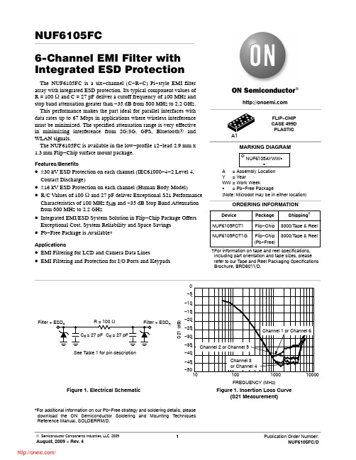
NUF6105FC6-Channel EMI Filter with Integrated ESD ProtectionThe NUF6105FC is a six −channel (C −R −C) Pi −style EMI filter array with integrated ESD protection. Its typical component values of R = 100 W and C = 27 pF deliver a cutoff frequency of 100 MHz and stop band attenuation greater than −35 dB from 800 MHz to 2.2 GHz.This performance makes the part ideal for parallel interfaces with data rates up to 67 Mbps in applications where wireless interference must be minimized. The specified attenuation range is very effective in minimizing interference from 2G/3G, GPS, Bluetooth ® and WLAN signals.The NUF6105FC is available in the low −profile 12−lead 2.9 mm x 1.3 mm Flip −Chip surface mount package.Features/Benefits•±30 kV ESD Protection on each channel (IEC61000−4−2 Level 4,Contact Discharge)•±16 kV ESD Protection on each channel (Human Body Model)•R/C Values of 100 W and 27 pF deliver Exceptional S21 Performance Characteristics of 100 MHz f 3dB and −35 dB Stop Band Attenuation from 800 MHz to 2.2 GHz•Integrated EMI/ESD System Solution in Flip −Chip Package Offers Exceptional Cost, System Reliability and Space Savings •Pb −Free Package is Available*Applications•EMI Filtering for LCD and Camera Data Lines•EMI Filtering and Protection for I/O Ports and KeypadsFigure 1. Electrical SchematicSee Table 1 for pin descriptionn−50−45−40−35−30−25−20−15−10−50Figure 1. Insertion Loss Curve(S21 Measurement)FREQUENCY (MHz)S 21 (d B )*For additional information on our Pb −Free strategy and soldering details, please download the ON Semiconductor Soldering and Mounting Techniques Reference Manual, SOLDERRM/D.Device Package Shipping †ORDERING INFORMATIONNUF6105FCT1Flip −Chip 3000/T ape & Reel FLIP −CHIP CASE 499D PLASTICNUF6105AYWW GGMARKING DIAGRAMA = Assembly Location Y = YearWW = Work Week G = Pb −Free Package(Note: Microdot may be in either location)†For information on tape and reel specifications,including part orientation and tape sizes, please refer to our T ape and Reel Packaging Specifications Brochure, BRD8011/D.NUF6105FCT1GFlip −Chip (Pb −Free)3000/T ape & ReelTable 1. FUNCTIONAL PIN DESCRIPTIONFilter Device Pins DescriptionFilter 1 1 & 12Filter + ESD Channel 1Filter 2 2 & 11Filter + ESD Channel 2Filter 3 3 & 10Filter + ESD Channel 3Filter 4 4 & 9Filter + ESD Channel 4Filter 5 5 & 8Filter + ESD Channel 5Filter 6 6 & 7Filter + ESD Channel 6Ground Pad GND GroundMAXIMUM RATINGSParameter Symbol Value UnitESD Discharge IEC61000−4−2Contact DischargeMachine ModelHuman Body Model V PP303016kVDC Power per Resistor P R100mW DC Power per Package P T600mW Junction Temperature T J150°C Operating Temperature Range T OP−40 to 85°C Storage Temperature Range T STG−55 to 150°C Maximum Lead Temperature for Soldering Purposes (1.8 in from case for 10 seconds)T L260°C Stresses exceeding Maximum Ratings may damage the device. Maximum Ratings are stress ratings only. Functional operation above the Recommended Operating Conditions is not implied. Extended exposure to stresses above the Recommended Operating Conditions may affect device reliability.ELECTRICAL CHARACTERISTICS (T J = 25°C unless otherwise noted)Parameter Symbol Test Conditions Min Typ Max Unit Maximum Reverse Working Voltage V RWM 5.0V Breakdown Voltage V BR I R = 10 mA 6.07.08.0V Leakage Current I R V RWM = 3.3 V100nA Resistance R A I R = 20 mA80100120W Diode Capacitance C d V R = 2.5 V, f = 1.0 MHz27pF Line Capacitance C L V R = 2.5 V, f = 1.0 MHz54pF3 dB Cut−Off Frequency (Note 1)f3dB Above this frequency,appreciable attenuation occurs100MHz6 dB Cut−Off Frequency (Note 1)f6dB Above this frequency,appreciable attenuation occurs180MHz1.50 W source and 50 W load termination.TYPICAL PERFORMANCE CURVES (T A = 25°C unless otherwise specified)−50−45−40−35−30−25−20−15−10−50Figure 1. Insertion Loss Curve(S21 Measurement)FREQUENCY (MHz)S 21(d B)−80−70−60−50−40−30−20−100Figure 2. Analog Crosstalk Curve(S41 Measurement)FREQUENCY (MHz)S 41 (d B )TEMPERATURE (°C)R E S I S T A N C E (W )9596979899100101102103104105−40−151035608500.51.01.52.001.02.03.04.05.0REVERSE VOLTAGE (V)N O R M A L I Z E D C A P A C I T A N C EFigure 3. Typical Capacitance vs.Reverse Biased Voltage(Normalized Capacitance Cd at 2.5 V)Figure 4. Resistance Over TemperatureTheory of OperationThe NUF6105FC combines ESD protection and EMI filtering conveniently into a small package for today’s size constrained applications. The capacitance inherent to a typical protection diode is utilized to provide the capacitance value necessary to create the desired frequency response based upon the series resistance in the filter. By combining this functionality into one device, a large number of discrete components are integrated into one small package saving valuable board space and reducing BOM count and cost in the application.Application ExampleThe accepted practice for specifying bandwidth in a filter is to use the 3 dB cutoff frequency. Utilizing points such as the 6 dB or 9 dB cutoff frequencies results in signal degradation in an application. This can be illustrated in an application example. A typical application would include EMI filtering of data lines in a camera or display interface.In such an example it is important to first understand the signal and its spectral content. By understanding these things, an appropriate filter can be selected for the desired application. A typical data signal is pattern of 1’s and 0’s transmitted over a line in a form similar to a square wave.The maximum frequency of such a signal would be the pattern 1-0-1-0 such that for a signal with a data rate of 100 Mbps, the maximum frequency component would be 50 MHz. The next item to consider is the spectral content of the signal, which can be understood with the Fourier seriesapproximation of a square wave, shown below in Equations 1 and 2 in the Fourier series approximation.From this it can be seen that a square wave consists of odd order harmonics and to fully construct a square wave n must go to infinity. However, to retain an acceptable portion of the waveform, the first two terms are generally sufficient. These two terms contain about 85% of the signal amplitude and allow a reasonable square wave to be reconstructed.Therefore, to reasonably pass a square wave of frequency x the minimum filter bandwidth necessary is 3x . All ON Semiconductor EMI filters are rated according to this principle. Attempting to violate this principle will result in significant rounding of the waveform and cause problems in transmitting the correct data. For example, take the filter with the response shown in Figure 5 and apply three different data waveforms. To calculate these three different frequencies, the 3 dB, 6 dB, and 9 dB bandwidths will be used.Equation 1:x(t)+12)2p aS n +1ƪ12n *1sin((2n *1)w 0t)ƫ(eq. 1)Equation 2 (simplified form of Equation 1):x(t)+12)2pƪsin(w 0t)1)sin(3w 0t)3)sin(5w 0t)5)AAA ƫ(eq. 2)M a g n i t u d e (d B )Frequency (Hz)100k 1M 100M1G 10G10M Figure 5. Filter BandwidthFrom the above paragraphs it is shown that the maximumsupported frequency of a waveform that can be passed through the filter can be found by dividing the bandwidth by a factor of three (to obtain the corresponding data ratemultiply the result by two). The following table gives the bandwidth values and the corresponding maximum supported frequencies and the third harmonic frequencies.Table 2. Frequency ChartBandwidth Maximum SupportedFrequencyThird Harmonic Frequency3 dB –100 MHz 33.33 MHz (f 1)100 MHz 6 dB –200 MHz 66.67 MHz (f 2)200 MHz 9 dB –300 MHz100 MHz (f 3)300 MHzConsidering that 85% of the amplitude of the square is in the first two terms of the Fourier series approximation most of the signal content is at the fundamental (maximum supported) frequency and the third harmonic frequency. If a signal with a frequency of 33.33 MHz is input to this filter,the first two terms are sufficiently passed such that the signal is only mildly affected, as is shown in Figure 6a. If a signalwith a frequency of 66.67 MHz is input to this same filter,the third harmonic term is significantly attenuated. This serves to round the signal edges and skew the waveform, as is shown in Figure 6b. In the case that a 100 MHz signal isinput to this filter, the third harmonic term is attenuated evenfurther and results in even more rounding of the signal edges as is shown in Figure 6c. The result is the degradation of the data being transmitted making the digital data (1’s and 0’s)more difficult to discern. This does not include effects of other components such as interconnect and other path losses which could further serve to degrade the signal integrity.While some filter products may specify the 6 dB or 9 dB bandwidths, actually using these to calculate supported frequencies (and corresponding data rates) results in significant signal degradation. To ensure the best signal integrity possible, it is best to use the 3 dB bandwidth to calculate the achievable data rate.Figure 6. Input and Output Waveforms of FilterInput WaveformOutput WaveformInput WaveformOutput WaveformInput WaveformOutput Waveforma) Frequency = f 1b) Frequency = f 2c) Frequency = f 3PACKAGE DIMENSIONS15 PIN FLIPCHIP CSPCASE 499D −01ISSUE ONOTES:1.DIMENSIONING AND TOLERANCING PER ASME Y14.5M, 1994.2.CONTROLLING DIMENSION: MILLIMETER.3.COPLANARITY APPLIES TO SPHERICAL CROWNS OF SOLDER BALLS.DIM A MIN MAX −−−MILLIMETERS A1A20.3800.430D 2.960 BSC E b 0.2900.340e 0.500 BSC 0.7000.2100.2701.330 BSC e10.435 BSC D10.870 BSCE12.500 BSC ON Semiconductor and are registered trademarks of Semiconductor Components Industries, LLC (SCILLC). SCILLC reserves the right to make changes without further notice to any products herein. SCILLC makes no warranty, representation or guarantee regarding the suitability of its products for any particular purpose, nor does SCILLC assume any liability arising out of the application or use of any product or circuit, and specifically disclaims any and all liability, including without limitation special, consequential or incidental damages.“Typical” parameters which may be provided in SCILLC data sheets and/or specifications can and do vary in different applications and actual performance may vary over time. All operating parameters, including “Typicals” must be validated for each customer application by customer’s technical experts. SCILLC does not convey any license under its patent rights nor the rights of others. SCILLC products are not designed, intended, or authorized for use as components in systems intended for surgical implant into the body, or other applications intended to support or sustain life, or for any other application in which the failure of the SCILLC product could create a situation where personal injury or death may occur. Should Buyer purchase or use SCILLC products for any such unintended or unauthorized application, Buyer shall indemnify and hold SCILLC and its officers, employees, subsidiaries, affiliates,and distributors harmless against all claims, costs, damages, and expenses, and reasonable attorney fees arising out of, directly or indirectly, any claim of personal injury or death associated with such unintended or unauthorized use, even if such claim alleges that SCILLC was negligent regarding the design or manufacture of the part. SCILLC is an Equal Opportunity/Affirmative Action Employer. This literature is subject to all applicable copyright laws and is not for resale in any manner.PUBLICATION ORDERING INFORMATIONBluetooth is a registered trade of Bluetooth SIG.分销商库存信息:ONSEMINUF6105FCT1G NUF6105FCT1。
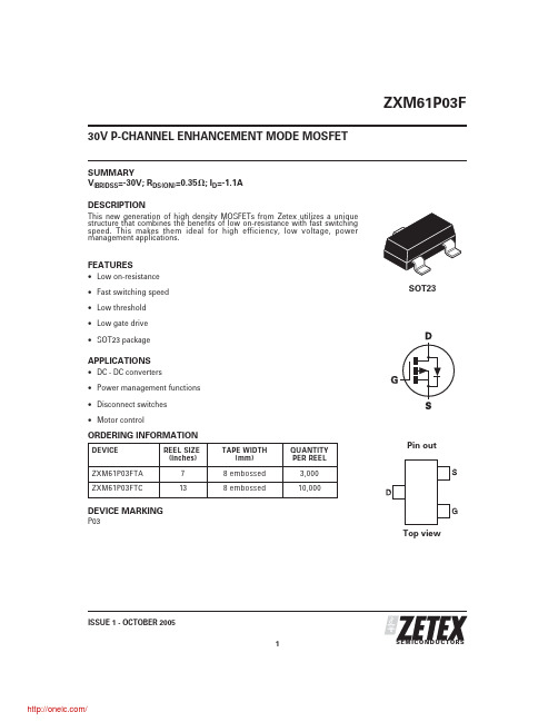
ZXM61P03FTA;ZXM61P03FTC;中文规格书,Datasheet资料
1S E M I C O N D U C T O R SZXM61P03FISSUE 1 - OCTOBER 200530V P-CHANNEL ENHANCEMENT MODE MOSFETSUMMARYV (BR)DSS =-30V; R DS(ON)=0.35⍀; I D =-1.1A DESCRIPTIONThis new generation of high density MOSFETs from Zetex utilizes a unique structure that combines the benefits of low on-resistance with fast switching speed.This makes them ideal for high efficiency,low voltage,power management applications.FEATURES•Low on-resistance •Fast switching speed •Low threshold •Low gate drive •SOT23 packageAPPLICATIONS•DC - DC converters•Power management functions •Disconnect switches •Motor controlORDERING INFORMATIONDEVICE REEL SIZE (inches)TAPE WIDTH(mm)QUANTITY PER REEL ZXM61P03FTA 78embossed 3,000ZXM61P03FTC138embossed10,000DEVICE MARKINGP03SOT23Pin outTop viewZXM61P03FS E M I C O N D U C T O R SISSUE 1 - OCTOBER 20052THERMAL RESISTANCEPARAMETERSYMBOL VALUE UNIT Junction to Ambient (a)R θJA 200°C/W Junction to Ambient (b)R θJA155°C/WNOTES:(a) For a device surface mounted on 25mm x 25mm FR4 PCB with high coverage of single sided 1oz copper, in still air conditions (b) For a device surface mounted on FR4 PCB measured at t р5 secs.(c) Repetitive rating - pulse width limited by maximum junction temperature. Refer to Transient Thermal Impedance graph.ABSOLUTE MAXIMUM RATINGSPARAMETERSYMBOL LIMIT UNIT Drain-Source Voltage V DSS -30V Gate-Source Voltage V GSϮ20VContinuous Drain Current(V GS =-10V;T A =25°C)(b)(V GS =-10V;T A =70°C)(b)I D -1.1-0.9A Pulsed Drain Current (c)I DM -4.3A Continuous Source Current (Body Diode)(b)I S -0.88A Pulsed Source Current (Body Diode)(c)I SM -4.3A Power Dissipation at T A =25°C (a)Linear Derating FactorP D 6255mW mW/°C Power Dissipation at T A =25°C (b)Linear Derating FactorP D 8066.4mW mW/°C Operating and Storage Temperature RangeT j :T stg-55 to +150°CZXM61P03FS E M I C O N D U C T O R SISSUE 1 - OCTOBER 20053CHARACTERISTICSZXM61P03FS E M I C O N D U C T O R SISSUE 1 - OCTOBER 20054ELECTRICAL CHARACTERISTICS (at T amb =25°C unless otherwise stated).PARAMETER SYMBOLMIN.TYP.MAX.UNIT CONDITIONS.STATICDrain-Source Breakdown Voltage V (BR)DSS -30V I D =-250µA,V GS =0V Zero Gate Voltage Drain Current I DSS -1µA V DS =-30V,V GS =0V Gate-Body LeakageI GSS Ϯ100nA V GS =Ϯ20V,V DS =0V Gate-Source Threshold VoltageV GS(th)-1.0V I D=-250µA,V DS =V GS Static Drain-Source On-State Resistance (1)R DS(on)0.350.55ΩΩV GS =-10V,I D =-0.6A V GS =-4.5V,I D =-0.3A Forward Transconductance (3)g fs0.44SV DS =-10V,I D =-0.3ADYNAMIC (3)Input Capacitance C iss 140pF V DS =-25V,V GS =0V,f=1MHzOutput CapacitanceC oss 45pF Reverse Transfer Capacitance C rss20pFSWITCHING (2)(3)Turn-On Delay Time t d(on) 1.9ns V DD =-15V,I D =-0.6A R G =6.2Ω,R D =25Ω(Refer to test circuit)Rise Timet r 2.9ns Turn-Off Delay Time t d(off)8.9ns Fall Timet f 5.0nsTotal Gate Charge Q g 4.8nC V DS =-24V,V GS =-10V,I D =-0.6A(Refer to test circuit)Gate-Source Charge Q gs 0.62nC Gate Drain Charge Q gd1.3nCSOURCE-DRAIN DIODE Diode Forward Voltage (1)V SD -0.95V T j =25°C,I S =-0.6A,V GS =0VReverse Recovery Time (3)t rr 14.8ns T j =25°C,I F =-0.6A,di/dt=100A/µsReverse Recovery Charge(3)Q rr7.7nCNOTES:(1) Measured under pulsed conditions. Width=300µs. Duty cycle Յ2%.(2) Switching characteristics are independent of operating junction temperature.(3) For design aid only, not subject to production testing.ZXM61P03FS E M I C O N D U C T O R SISSUE 1 - OCTOBER 20055TYPICAL CHARACTERISTICSZXM61P03FS E M I C O N D U C T O R SISSUE 1 - OCTOBER 20056TYPICAL CHARACTERISTICSZXM61P03FS E M I C O N D U C T O R SISSUE 1 - OCTOBER 20057EuropeZetex GmbHStreitfeldstraße 19D-81673 München GermanyTelefon: (49) 89 45 49 49 0Fax: (49) 89 45 49 49 49europe.sales@AmericasZetex Inc700 Veterans Memorial Hwy Hauppauge, NY 11788USATelephone: (1) 631 360 2222Fax: (1) 631 360 8222usa.sales@Asia PacificZetex (Asia) Ltd3701-04Metroplaza Tower 1Hing Fong Road, Kwai Fong Hong KongTelephone: (852) 26100 611Fax: (852) 24250 494asia.sales@Corporate Headquarters Zetex Semiconductors plc Zetex Technology ParkChadderton, Oldham, OL9 9LL United KingdomTelephone (44) 161 622 4444Fax: (44) 161 622 4446hq@These offices are supported by agents and distributors in major countries world-wide.This publication is issued to provide outline information only which (unless agreed by the Company in writing)may not be used,applied or reproduced for any purpose or form part of any order or contract or be regarded as a representation relating to the products or services concerned.The Company reserves the right to alter without notice the specification, design, price or conditions of supply of any product or service.For the latest product information,log on to ©ZetexSemiconductors plc 2005PACKAGE DETAILSPAD LAYOUT DETAILSDIM MillimetersInches DIM Millimeters Inches Min Max Min Max Min Max Max Max A 2.67 3.050.1050.120H 0.330.510.0130.020B 1.20 1.400.0470.055K 0.010.100.00040.004C ᎏ 1.10ᎏ0.043L 2.10 2.500.0830.0985D 0.370.530.0150.021M 0.450.640.0180.025F 0.0850.150.00340.0059N 0.95 NOM 0.0375 NOMG1.90 NOM 0.075 NOMᎏᎏᎏPACKAGE DIMENSIONS分销商库存信息:DIODESZXM61P03FTA ZXM61P03FTC。
DPG60C200HB;中文规格书,Datasheet资料

HiPerFRED²Features / Advantages:Applications:Package:Part numberV I RRM ==20030DPG 60 C 200 HBV A 2x Backside: cathodet rr =35nsHigh Performance Fast Recovery Diode Low Loss and Soft Recovery Common Cathode● Planar passivated chips● Very low leakage current ● Very short recovery time ● Improved thermal behaviour ● Very low Irm-values● Very soft recovery behaviour● Avalanche voltage rated for reliable operation ● Soft reverse recovery for low EMI/RFI ● Low Irm reduces:- Power dissipation within the diode- Turn-on loss in the commutating switch● Antiparallel diode for high frequency switching devices ● Antisaturation diode ● Snubber diode● Free wheeling diode● Rectifiers in switch mode power supplies (SMPS)● Uninterruptible power supplies (UPS)FAVI RMS A per pin 50R thCH K/W 0.25M D Nm 1.2mounting torque 0.8T stg °C 150storage temperature-55Weight g 6Symbol DefinitionRatingstyp.max.min.Conditions RMS currentthermal resistance case to heatsink Unit I is typically limited by: 1. pin-to-chip resistance; or by 2. current capability of the chip.In case of 1, a common cathode/anode configuration and a non-isolated backside, the whole current capability can be used by connecting the backside.F CN120mounting force with clip20Ordering Delivering ModeBase Qty Code KeyStandard Part Name DPG 60 C 200 HB 506294Tube 30D P G 60C 200 HBPart numberDiodeHiPerFRED extreme fastCommon CathodeT O-247AD (3) ===DPG60C200QB DPF60C200HB DPF60C200HJ TO-3P (3)TO-247AD (3)ISOPLUS247 (3)Similar PartPackage1)1)Marking on Product DPG60C200HB 200200200Voltage ClassCurrent Rating [A]Reverse Voltage [V]====RMS分销商库存信息: IXYSDPG60C200HB。
SBR20U150CTFP;中文规格书,Datasheet资料

20A SBR®Super Barrier RectifierFeatures MechanicalData• Case Material: Molded Plastic, UL FlammabilityClassification Rating 94V-0• Moisture Sensitivity: Level 1 per J-STD-020C• Terminals: Matte Tin Finish annealed overCopper leadframe. Solderable per MIL-STD-202,Method 208• Marking: See Page 4• Ordering Information: See Page 4• Low Forward Voltage Drop• Excellent High Temperature Stability• Super Barrier Design• Soft, Fast Switching Capability• Molded Plastic TO-220AB,and ITO-220AB packages• Lead Free Finish, RoHS Compliant (Note 2)Maximum Ratings @ T A = 25ºC unless otherwise specifiedSingle phase, half wave, 60Hz, resistive or inductive load.For capacitive load, derate current by 20%.Characteristic SymbolValueUnit Peak Repetitive Reverse VoltageWorking Peak Reverse VoltageDC Blocking VoltageV RRMV RWMV RM150 VRMS Reverse Voltage V R(RMS)106 VAverage Rectified Output Current @ T C = 140ºC I O20 ANon-Repetitive Peak Forward Surge Current 8.3msSingle Half Sine-Wave Superimposed on Rated LoadI FSM200 APeak Repetitive Reverse Surge Current (2uS-1Khz) I RRM 3 AMaximum Thermal Resistance (per leg)Package = TO-220ABPackage = ITO-220ABRӨJC 24°C/WOperating and Storage Temperature Range T J, T STG-65 to +175 ºCElectrical Characteristics@ T A = 25ºC unless otherwise specifiedCharacteristic SymbolMin Typ Max Unit Test ConditionReverse Breakdown Voltage (Note 1) V(BR)R150 - - V I R = 0.5 mAForward Voltage Drop V F--0.62-0.780.650.86VI F = 10A, T J = 25ºCI F = 10A,T J = 125ºCI F = 20A, T J = 25ºCLeakage Current (Note 1) I R- -0.525mAV R = 150V, T J= 25 ºCV R = 150V, T J = 125 ºCNotes:1. Short duration pulse test used to minimize self-heating effect.2. RoHS revision 13.2.2003. High temperature solder exemption applied, see EU Directive Annex Note 7.__________SBR is a registered trademark of Diodes Incorporated.Package Outline DrawingsTO-220ABTO-220ABDIM. MIN. MAX.A 4.47 4.67b 0.71 0.91b1 1.17 1.37c 0.31 0.53D 14.65 15.35D1 8.50 8.90E 10.01 10.31e 2.54type1 4.98 5.18F 1.17 1.37J1 2.52 2.82L 13.40 13.80L1 3.56 3.96ØP 3.735 3.935Q 2.59 2.89All Dimensions in MillimetersITO-220ABITO-220ABDIM. MIN. MAX.A 4.30 4.70b 0.50 0.75b1 1.10 1.35b2 1.50 1.75c 0.50 0.75D 14.80 15.20E 9.96 10.36e 2.54typF 2.80 3.20J1 2.50 2.90L 12.80 13.60L1 1.70 1.90ØP 3.50typQ 2.70typAll Dimensions in MillimetersMarking, Polarity, Weight & Ordering InformationSBR20U150CT SBR20U150CTFP Case StyleTO-220AB ITO-220ABtAnodeCommonCathode AnodePolarityCasetAnodeCommonCathode AnodeMarking2.1g 1.9gWeightOrderingInformationSBR20U150CT SBR20U150CTFP50 pieces/tube50 pieces/tubeYY = Last two digits of year, ex = 06 = 2006Date CodeWW = Week (01-52)Other MarkingInformationA = Foundry CodeB = Assembly CodeIMPORTANT NOTICEDiodes Incorporated and its subsidiaries reserve the right to make modifications, enhancements, improvements, corrections or other changeswithout further notice to any product herein. Diodes Incorporated does not assume any liability arising out of the application or use of any productdescribed herein; neither does it convey any license under its patent rights, nor the rights of others. The user of products in such applications shallassume all risks of such use and will agree to hold Diodes Incorporated and all the companies whose products are represented on our website,harmless against all damages.LIFE SUPPORTDiodes Incorporated products are not authorized for use as critical components in life support devices or systems without the expressed writtenapproval of the President of Diodes Incorporated.分销商库存信息: DIODESSBR20U150CTFP。
