FQPF8P10中文资料
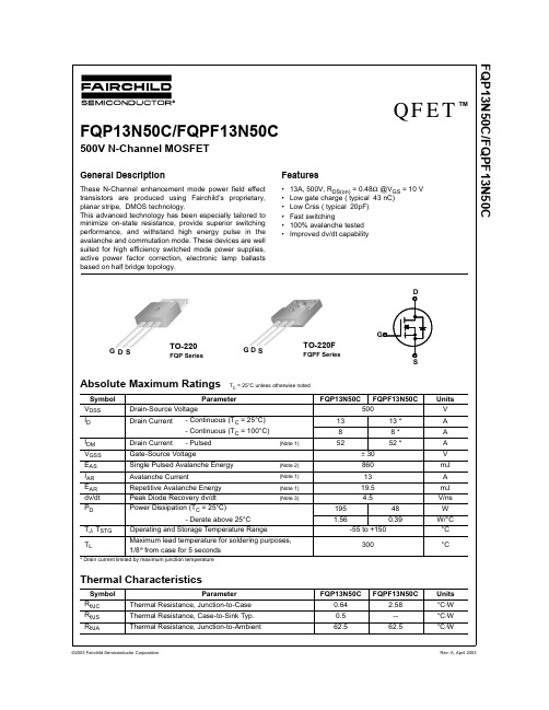
FQP13N50C中文资料
--
--
IGSSF IGSSR
Gate-Body Leakage Current, Forward VGS = 30 V, VDS = 0 V Gate-Body Leakage Current, Reverse VGS = -30 V, VDS = 0 V
--
--
--
--
--
--
1 10 100 -100
FQP13N50C FQPF13N50C
500
13
13 *
8
8*
52
52 *
± 30
860
13
19.5
4.5
195
48
1.56
0.39
-55 to +150
300
Units V A A A V mJ A mJ
V/ns W
W/°C °C
°C
Thermal Characteristics
Symbol RθJC RθJS RθJA
2.0 --
4.0
V
VGS = 10 V, ID = 6.5 A
-- 0.39 0.48
Ω
VDS = 40 V, ID = 6.5 A
(Note 4) --
15
--
S
Dynamic Characteristics
Ciss
Input Capacitance
Coss
Output Capacitance
Crss
Drain Current - Continuous (TC = 25°C)
- Continuous (TC = 100°C)
IDM
Drain Current - Pulsed
8位机讲义

存储器结构
内部数据存储器
内部数据存储器被划分为物理上分开的两个不同的区域: 256B RAM和128B 特殊功能寄存器(SFR)区。RAM的 高128B和SFR区共用相同的地址段,通过不同的寻址方式 访问。RAM的低128B可通过直接寻址或寄存器间接寻址 方式访问;RAM的高128B只能通过寄存器间接寻址方式 访问;SFR只能通过直接寻址方式访问。RAM的地址段 20H到2FH的16个字节可位寻址;地址段30H到7FH可用作 暂存寄存器或堆栈。
存储器结构
程序存储器
使用一个专用接口使CPU和程序存储器直接 相连(而无需任何引脚连接),CPU的性能 得到优化。这意味着在每个时钟的上升沿均 能读取代码。因此,这里不存在“内部”或 “外 部”程序存储器的概念,因为所有的代码均 从 同一个程序存储器接口存取。
存储器结构
数据存储器
数据存储器由内部存储器和外部存储器组成。 数据存储器的“内部”和“外部”标记用来 区分寄 存器存储器和使用“MOVX”指令存取数据的 64 KB数据存储器。该外部标记并非暗指外部数 据存储器位于片外。
存储器结构
XC886/888的CPU可寻址以下五个地址空间:
12KB启动ROM(BootROM)程序存储器 256B内部RAM数据存储器 1.5KB XRAM存储器(XRAM可作为程序存储器或外部数 据存储器进行读写) 128B SFR区 24/32KB Flash程序存储器(Flash器件);或24/32KB ROM程序存储器,外加4KB Flash(ROM器件)
功能概述
法的十进制的调整和比较。逻辑运算包括与、 或、异或、补码和循环移位(右环移、左环 移、或4位环移(半字节交换))。ALU还包 括一个布尔处理机,可执行置位、清零、补 码、等于1跳转、等于0跳转、等于1跳转并清 零,送入/取自进位位的位操作。在任意可寻 址位(或该位补码)和进位标志之间,可执
FQD8P10中文资料

Figure 1. On-Region Characteristics
1.5
1.2
V = - 10V GS
0.9
VGS = - 20V
0.6
0.3
※ Note : TJ = 25℃
0.0
0
5
10
15
20
25
-ID , Drain Current [A]
Figure 3. On-Resistance Variation vs. Drain Current and Gate Voltage
Parameter
Drain-Source Voltage
Drain Current
- Continuous (TC = 25°C) - Continuous (TC = 100°C)
Drain Current - Pulsed
(Note 1)
Gate-Source Voltage
Single Pulsed Avalanche Energy
-IDR , Reverse Drain Current [A]
-ID , Drain Current [A]
101
100 10-1
2
150℃
25℃
-55℃
※ Notes : 1. VDS = -40V 2. 250μ s Pulse Test
4
6
8
10
-VGS , Gate-Source Voltage [V]
©2002 Fairchild Semiconductor Corporation
Rev. B, August 2002
元器件交易网
FQD8P10 / FQU8P10
FPGA可编程逻辑器件芯片XC95108-10PQ100I中文规格书
Chapter 1:Configuration OverviewCreating an Encrypted BitstreamBitGen, provided with the Xilinx ISE software, can generate encrypted as well as non-encrypted bitstreams. For AES bitstream encryption, the user specifies a 256-bit key as aninput to BitGen. BitGen in turn generates an encrypted bitstream file (BIT) and anencryption key file (NKY).For specific BitGen commands and syntax, refer to the Development System Reference Guide.Loading the Encryption KeyThe encryption key can only be loaded onto a Virtex-5 device through the JTAG interface.The iMPACT tool, provided with the Xilinx ISE software, can accept the NKY file as aninput and program the device with the key through JTAG, using a supported Xilinxprogramming cable.To program the key, the device enters a special key-access mode using theISC_PROGRAM_KEY instruction. In this mode, all FPGA memory, including theencryption key and configuration memory, is cleared. After the key is programmed andthe key-access mode is exited, the key cannot be read out of the device by any means, andit cannot be reprogrammed without clearing the entire device. The key-access mode istransparent to most users.Loading Encrypted BitstreamsOnce the device has been programmed with the correct encryption key, the device can beconfigured with an encrypted bitstream. After configuration with an encrypted bitstream,it is not possible to read the configuration memory through JTAG or SelectMAP readback,regardless of the BitGen security setting.While the device holds an encryption key, a non-encrypted bitstream can be used toconfigure the device; in this case the key is ignored. After configuring with a non-encrypted bitstream, readback is possible (if allowed by the BitGen security setting). Theencryption key still cannot be read out of the device, preventing the use of Trojan Horsebitstreams to defeat the Virtex-5 encryption scheme.The method of configuration is not affected by encryption. The configuration bitstream canbe delivered in any mode (Serial, JTAG, or any x8 parallel modes) from any configurationsolution (PROM, System ACE™ controller, etc.). The x16 and x32 bus widths are notsupported for encrypted bitstreams. Configuration timing and signaling are alsounaffected by encryption.The encrypted bitstream must configure the entire device because partial reconfigurationthrough any configuration interface is not permitted for encrypted bitstreams. Afterconfiguration, the device cannot be reconfigured without toggling the PROGRAM_B pin,cycling power, or issuing the JPROGRAM instruction. Fallback reconfiguration andIPROG reconfiguration (see “Fallback MultiBoot,” page153) are disabled after encryptionis turned on. Readback is available through the ICAP primitive (see “Bitstream Encryptionand Internal Configuration Access Port (ICAP)”). None of these events resets the key ifV BATT or V CCAUX is maintained.A mismatch between the key in the encrypted bitstream and the key stored in the devicecauses configuration to fail with the INIT_B pin going Low and the DONE pin remainingLow.Bitstream EncryptionBitstream Encryption and Internal Configuration Access Port (ICAP) The Internal Configuration Access Port (ICAP) primitive provides the user logic withaccess to the Virtex-5 configuration interface. The ICAP interface is similar to theSelectMAP interface, although the restrictions on readback for the SelectMAP interface donot apply to the ICAP interface after configuration. Users can perform readback throughthe ICAP interface even if bitstream encryption is used. Unless the designer wires the ICAPinterface to user I/O, this interface does not offer attackers a method for defeating theVirtex-5 AES encryption scheme.Users concerned about the security of their design should not:∙Wire the ICAP interface to user I/O-or-∙Instantiate the ICAP primitive.Like the other configuration interfaces, the ICAP interface does not provide access to thekey register.V BATTThe encryption key memory cells are volatile and must receive continuous power to retaintheir contents. During normal operation, these memory cells are powered by the auxiliaryvoltage input (V CCAUX), although a separate V BATT power input is provided for retainingthe key when V CCAUX is removed. Because V BATT draws very little current (on the order ofnanoamperes), a small watch battery is suitable for this supply. (To estimate the battery life,refer to V BATT DC Characteristics in DS202, Virtex-5 Data Sheet: DC and SwitchingCharacteristics and the battery specifications.) At less than a 100nA load, the endurance ofthe battery should be limited only by its shelf life.V BATT does not draw any current and can be removed while V CCAUX is applied. V BATTcannot be used for any purpose other than retaining the encryption keys when V CCAUX isremoved.Chapter 1:Configuration OverviewSelectMAP Configuration Interface PROM files for ganged serial configuration are identical to the PROM files used toconfigure single devices. There are no special PROM file considerations.SelectMAP Configuration InterfaceThe SelectMAP configuration interface (Figure2-6) provides an 8-bit, 16-bit, or 32-bitbidirectional data bus interface to the Virtex-5 configuration logic that can be used for bothconfiguration and readback. (For details, refer to Chapter7, “Readback and ConfigurationVerification.”) The bus width of SelectMAP is automatically detected (see “Bus Width AutoDetection”).CCLK is an output in Master SelectMAP mode; in Slave SelectMAP, CCLK is an input. Oneor more Virtex-5 devices can be configured through the SelectMAP bus.There are four methods of configuring an FPGA in SelectMAP mode:∙Single device Master SelectMAP∙Single device Slave SelectMAP∙Multiple device SelectMAP bus∙Multiple device ganged SelectMAPTable2-4 describes the SelectMAP configuration interface.Figure 2-6:Virtex-5 Device SelectMAP Configuration InterfaceTable 2-4:Virtex-5 Device SelectMAP Configuration Interface PinsPin Name Type Dedicatedor Dual-PurposeDescriptionM[2:0]Input Dedicated Mode pins - determine configuration modeCCLK Input andOutputDedicatedConfiguration clock source for all configurationmodes except JTAGD[31:0]Three-StateBidirectionalDual-PurposeConfiguration and readback data bus, clockedon the rising edge of CCLK. See “Parallel BusBit Order” and Table1-2.BU S YDONECCLKPROGRAM_BINIT_BD[31:0]M[2:0]C S_BRDWR_BC S O_BUG191_c2_10_072407Board Layout for Configuration Clock (CCLK)。
HFS8中文资料

>RO^_\R]*/.~}x 2|,x 99;AY[_^XZQ_WR<;AY[_^XZQ_WR mml 6xz 4RI>npl 6xz 4RI>mn 6{z 4RI>np 6{z 4RI>+GINM OHEM:@>K:G@>tl MH mon 6xz mrl MH nrq 6xzujr MH ntjt 6{z2:MBG@BGINM <NKK>GMs F x 0HP>K ?K>JN>G<R K:G@>ps MH ro *S iiii-NLM HI>K:M>OHEM:@>tl 6xz mrl 6xz ujr 6{z -NLM K>E>:L>OHEM:@>ol 6xz pl 6xzqjl 6{z{z LNIIER OHEM:@>e 6==f p MH r 6{z -:Q j HNMINM <NKK>GM p F x e :M q 6{zf/NMINM EH@B</I>K:M>PBMA G>@:MBO>MKN>EH@B<e :<MBO>EHP f -:Q j MNKG i HG MBF>nq FL ml FL -:Q j MNKG i H??MBF>ol FLml FL+GLNE:MBHG K>LBLM:G<>mlll -e :M qll 6{zf {B>E><MKB<LMK>G@MA e BGINM MH HNMINM f nqll 6xzh ql *S krl *S h m FBG /I>K:MBG@M>FI>K:MNK>K:G@>iol MH tl 3MHK:@>M>FI>K:MNK>K:G@>iolMH mllz :L><HEHK 9>EEHP 7ABM>5GBM P>B@AMx IIKHQ j ojq @+.054LB=>/54054LB=>q F xe :M mpjp 6{zfml F xe :M ntjt 6{zfA0F XZQ_WR+.054/54054mj 3HE=>KBG@FNLM ;><HFIE>M>=PBMABG ml L><HG=L :M HK E>LL HK PBMABG q L><HG=L :M HK E>LL jnj 4H HNMINM FH=NE>h MA>332<:L>L>KO>L MH =BLLBI:M>A>:M j +GLM:EE MA>K>E:RL LH MA:M MA>R :K>:=>JN:M>ER O>GMBE:M>=j +?IHHKO>GMBE:MBHG BLNG:OHB=:;E>h K>=N<>MA>EH:=<NKK>GM ;R A:E?joj 7A>G NLBG@MA>*}3te HNMINM FH=NE>f L>KB>L ?HK :G xz EH:=PBMA :I>:D OHEM:@>H?FHK>MA:G pql 6h <HGG><M MA>EH:=M>KFBG:EL H?MA>K>E:R MH :G BGKNLA :;LHK;>K e O:KBLMHK f j 4A>K><HFF>G=>=O:KBLMHK OHEM:@>h ppl MH psl 6j+3/ullm X+3/k 43mrupu X+3/mpllm X/*3x 3mtllm z|24+}+|{nlls 2>O j mjll}BE>.H jv z 1zlollmllrqtnA^RX @>I7,B?;/7>-AEGKJ DF<KC=0AHMH BLHE:MBHG+k /FH=NE>L?HK BGM>K?:<>;>MP>>G z 05:G=>QM>KG:E BGI NM =>OB<>LHK EH:=L jnqll 6=B>E><MKB<LMK>G@MA j 0KBGM>=<BK<NBM ;H:K=FHNGM 2H*3<HFIEB:GMZ Z Z Z Z GH=;9KJAFEIIG=;A>A;9JAFEI e 4x w nqfFKJGKJ DF<KC=FH<=HAE?AE>FHD9JAFEEZ^R]8*}3t BL:G>GOBKHGF>GM:E?KB>G=ER IKH=N<M h IE>:L>F:KD LI><B:E<H=>eqqqf PA>G HK=>K jAY[_^XZQ_WR/NMEBG>{BF>GLBHGL0zy ,:RHNM7BKBG@{B:@K:Fxz BGINM MRI>{z BGINM MRI>6==/NM ~G=ey HMMHF OB>P fey HMMHF OB>P fFKJCAE=<AD=EIAFEI.MAHAE?<A9?H9D 9E<G;:F9H<C9NFKJ 5GBMv FFgki ikg +GINM /NMINMEZ^R]8*}3t BL:G >GOBKHGF>GM:E ?KB>G=ER IKH=N<M h IE>:L>F:KD LI><B:E <H=>eqqqf PA>G HK=>K jEZ^R]8*}3t BL:G >GOBKHGF>GM:E ?KB>G=ER IKH=N<M h IE>:L>F:KD LI><B:E <H=>eqqqf PA>G HK=>K jx F;B>GM M>FI>K:MNK>e -:Q j ,H:=z NKK>GM OL j x F;B>GM 4>FI>K:MNK>e /NMINM FH=NE>fF_^[_^XZQ_WR/NMEBG>{BF>GLBHGL0zy ,:RHNMxz HNMINM MRI>7BKBG@{B:@K:F{z HNMINM MRI>{BL<E:BF>K4ABL =:M:LA>>M BL ?HK MA><NLMHF>KLU K>?>K>G<>j x EE MA>LI><B?B<:MBHGL :K>LN;C><M MH <A:G@>PBMAHNM GHMB<>j 7><HNE=GHM >O:EN:M>:EE MA>I >K?HKF:G<>:G=:EE MA>I :K:F>M>KL?HK >O>KR I HL L B;E>:I I EB<:MBHG j 4ANL MA>NL>K LAHNE=;>BG :KB@AM IHLBMBHG MH <AHHL>MA>LNBM:;E>IKH=N<M ?HK MA>BK HPG :IIEB<:MBHG j +?MA>K>BL:GR JN>KR h IE>:L><HGM:<M *HG@?:?HK MA>M><AGB<:E L>KOB<>j *HP>O>K h BM BL MA>NL>KUL K>LIHGLB;BEBMR MH =>M>KFBG>PAB<A IKH=N<M LAHNE=;>NL>=HGER jT 8B:F>G *HG@?:|E><MKH:<HNLMB<z H jh ,M=j x EE KB@AMLH?*HG@?::K>K>L >KO>=jey HMMHF OB>P fey HMMHF OB>P f,H :=z N K K >G M e 2-3f e x fFKJCAE=<AD=EIAFEI.MAHAE?<A9?H9D 9E<G;:F9H<C9NFKJ ;@9H9;J=HAIJA;;KHL=I5GBM v FFm ljr ljt ljn lljp rl l nl pl iol inl mlltlnq。
P8P中文资料
Fully Sealed Container Cermet Trimmers For technical questions, contact: sfer@See also: Application notesDocument Number: 5101948Revision: 26-Oct-06P8PVishay SferniceFEATURES•Military and professional grade •1 Watt at 70 °C, P8PT•0.5 Watt at 70 °C, P8PX - P8PY •CECC 41 101-002 (A, B)•GAM T1•Fully sealedP8P series are available in three mounting configurations:- P8PX, side adjust with pins - P8PY, top adjust with pins - P8PT, panel mount with solder lugs•Multi-finger wiper contact in precious metalModels P8PX and P8PY feature a TO-5 transistor type,rugged metal case housing.The cermet track is printed to an alumina substrate allowing high dissipation and ensuring reliable performance under extreme environmental conditions.Models P8PX and P8PY are qualified PC 39 and PC 19respectively according to CECC 41 101-002 mod. A and B.DIMENSIONS in millimetersP8PX - (PC 39) B• Tolerance unless otherwise specified: ± 0.5P8PTCIRCUIT DIAGRAM}Outlets PCB mountingDocument Number: 51019For technical questions, contact: sfer@See also: Application notes Revision: 26-Oct-0649P8PFully Sealed Container Cermet TrimmersVishay SferniceELECTRICAL SPECIFICATIONSResistive Element cermet Electrical Travel 270° ± 15°Resistance Range 10 Ω to 2.2 M ΩStandard series E3 1 - 2.2 - 4.7 and on request 1 - 2 - 5Tolerance Standard ± 10 %On Request ± 5 %Power RatingP8PX - P8PY 0.5 W at 70 °C P8PT1 W at 70 °CTemperature CoefficientSee Standard Resistance Element T ableLimiting Element Voltage (Linear Law)250 VContact Resistance Variation 2 % Rn or 1 ΩEnd Resistance (Typical) 1 Ω Dielectric Strength (RMS)1000 V Insulation Resistance (500 VDC)1 GΩMECHANICAL SPECIFICATIONSMechanical Travel300° ± 5°Operating Torque (max. Ncm)3End Stop Torque (max. Ncm)6Unit Weight (max. g)1... 3.1ENVIRONMENTAL SPECIFICATIONSTemperature Range - 55 °C to + 125 °C Climatic Category 55/125/56Sealingfully sealed container IP67POWER RATING CHARTPERFORMANCECECC 41100TYPICAL VALUES AND DRIFTS TESTSCONDITIONSΔRTRT (%)REQUIREMENTS ΔR 1-2R 1-2(%) ΔRTRT (%) ΔR 1-2R 1-2(%)Climatic SequencePhase A dry heat 125 °C Phase B damp heat Phase C cold - 55 °CPhase D damp heat 5 cycles± 2 %± 3 %± 0.5 %± 1 %Long Term Damp Heat56 days 40 °C, 93 % RH ± 2 %± 3 %± 0.5 %± 1 %Dielectric strength: 700 VInsulation resistance: > 100 M ΩDielectric strength: 1000 V Insulation resistance: > 104 M ΩRotational Life 200 cycles± 2 %± 1 %Contact res. variat.: < 5 % Rn Contact res. variat.: < 2 % Rn Load Life1000 h at rated power 90’/30’ - ambient temp. 70 °C± 2 %± 3 %± 1 %± 2 %Contact res. variat.: < 5 % Rn Contact res. variat.: < 1 % Rn Rapid Temperature Change 5 cycles- 55 °C to + 125 °C ± 1.5 %ΔV 1-2V 1-3≤ ± 1 %± 0.2 %ΔV 1-2V 1-3≤ ± 0.5 %Shock50 g at 11 m secs 3 successive shocks in 3 directions ± 1 %± 2 %± 0.1 %± 0.5 %Vibration 10 - 55 Hz 0.75 mm or 10 g during 6 hours± 1 %ΔV 1-2V 1-3≤ ± 2 %± 0.2 %ΔV 1-2V6≤ ± 0.5 % For technical questions, contact: sfer@See also: Application notesDocument Number: 5101950Revision: 26-Oct-06P8PVishay SferniceFully Sealed Container Cermet TrimmersSTANDARD RESISTANCE ELEMENT DATASTANDARD RESISTANCE VALUESP8PX - P8PYP8PT TCR - 55 °C + 125 °C MAX.POWER AT 70 °CMAX.WORKING VOLTAGEMAX. CUR.THROUGH WIPERMAX.POWER AT 70 °CMAX.WORKING VOLTAGEMAX. CUR.THROUGH WIPERΩW V mA W V mA ppm/°C 102247 0.52.23.34.822415010313.164.696.863162131460+ 2001002204701K 2.2K 4.7K 10K 22K 47K 100K 220K 470K 1M 2.2M0.50.280.130.060.028710.515.322.433.248.57.710515322425025025025070473222151074.83.22.21.11.530.250.1110.630.280.130.060.0310.014.821.731.646.968.6100.0148217250250250250250100674632211510.06.74.62.51.10.50.30.1± 100MARKINGPrinted :- VISHAY trademark - NF type if applicable - series - style- ohmic value (in Ω , k Ω, M Ω)- tolerance (in %)- manufacturing date - marking of terminal: 3PACKAGING- Plastic box of 50 pieces for P8PX and P8PY - Plastic box of 24 pieces for P8PTORDERING INFORMATIONP8MODEL PY STYLE 10 k ΩOHMIC VALUE ± 10 %TOLERANCE BL50PACKAGING e2LEAD FINISHP8PX and P8PY: BL50P8PT: BL24e2: SnAg alloyDocument Number: 91000Revision: 18-Jul-081DisclaimerLegal Disclaimer NoticeVishayAll product specifications and data are subject to change without notice.Vishay Intertechnology, Inc., its affiliates, agents, and employees, and all persons acting on its or their behalf (collectively, “Vishay”), disclaim any and all liability for any errors, inaccuracies or incompleteness contained herein or in any other disclosure relating to any product.Vishay disclaims any and all liability arising out of the use or application of any product described herein or of any information provided herein to the maximum extent permitted by law. The product specifications do not expand or otherwise modify Vishay’s terms and conditions of purchase, including but not limited to the warranty expressed therein, which apply to these products.No license, express or implied, by estoppel or otherwise, to any intellectual property rights is granted by this document or by any conduct of Vishay.The products shown herein are not designed for use in medical, life-saving, or life-sustaining applications unless otherwise expressly indicated. Customers using or selling Vishay products not expressly indicated for use in such applications do so entirely at their own risk and agree to fully indemnify Vishay for any damages arising or resulting from such use or sale. Please contact authorized Vishay personnel to obtain written terms and conditions regarding products designed for such applications.Product names and markings noted herein may be trademarks of their respective owners.元器件交易网。
8TQ100中文资料

Document Number: 93414For technical questions, contact: diodes-tech@Schottky Rectifier, 8 A8TQ... SeriesVishay High Power ProductsFEATURES•175 °C T J operation•Low forward voltage drop •High frequency operation•H igh purity, high temperature epoxy encapsulation for enhanced mechanical strength and moisture resistance•Guard ring for enhanced ruggedness and long term reliability•Designed and qualified for industrial levelDESCRIPTIONThe 8TQ... Schottky rectifier series has been optimized for low reverse leakage at high temperature. The proprietary barrier technology allows for reliable operation up to 175 °C junction temperature. Typical applications are in switching power supplies, converters, freewheeling diodes, and reverse battery protection.PRODUCT SUMMARYI F(AV)8 A V R80/100 VTO-220ACMAJOR RATINGS AND CHARACTERISTICSSYMBOL CHARACTERISTICS VALUESUNITS I F(AV)Rectangular waveform8A V RRM Range 80/100V I FSM t p = 5 µs sine 850A V F 8 Apk, T J = 125 °C 0.58V T JRange- 55 to 175°CVOLTAGE RATINGSPARAMETER SYMBOL 8TQ0808TQ100UNITS Maximum DC reverse voltageV R 80100VMaximum working peak reverse voltageV RWMABSOLUTE MAXIMUM RATINGSPARAMETER SYMBOL TEST CONDITIONSVALUESUNITS Maximum average forward current See fig. 5I F(AV)50 % duty cycle at T C = 157 °C, rectangular waveform 8AMaximum peak one cycle non-repetitive surge current See fig. 7I FSM 5 µs sine or 3 µs rect. pulseFollowing any rated loadcondition and with rated V RRM applied850A10 ms sine or 6 ms rect. pulse230Non-repetitive avalanche energy E AS T J = 25 °C, I AS = 0.50 A, L = 60 mH7.50mJ Repetitive avalanche currentI ARCurrent decaying linearly to zero in 1 µsFrequency limited by T J maximum V A = 1.5 x V R typical0.50A 元器件交易网For technical questions, contact: diodes-tech@Document Number: 934148TQ... SeriesVishay High Power ProductsSchottky Rectifier, 8 ANote(1)Pulse width < 300 µs, duty cycle < 2 %ELECTRICAL SPECIFICATIONSPARAMETER SYMBOLTEST CONDITIONSVALUES UNITSMaximum forward voltage drop See fig. 1V FM (1)8 AT J = 25 °C 0.72V 16 A 0.888 A T J = 125 °C 0.5816 A0.69Maximum reverse leakage current See fig. 2I RM (1)T J = 25 °C V R = rated V R0.55mA T J = 125 °C7Maximum junction capacitance C T V R = 5 V DC (test signal range 100 kHz to 1 MHz) 25 °C 500pF Typical series inductance L S Measured lead to lead 5 mm from package body 8nH Maximum voltage rate of change dV/dtRated V R10 000V/µs THERMAL - MECHANICAL SPECIFICATIONSPARAMETER SYMBOL TEST CONDITIONSVALUES UNITS Maximum junction and storagetemperature rangeT J , T Stg - 55 to 175°CMaximum thermal resistance, junction to caseR thJC DC operation See fig. 42.0°C/WTypical thermal resistance, case to heatsink R thCSMounting surface, smooth and greased0.50Approximate weight 2g 0.07oz.Mounting torque minimum 6 (5)kgf · cm (lbf · in)maximum12 (10)Marking deviceCase style TO-220AC8TQ0808TQ100元器件交易网Document Number: 93414For technical questions, contact: diodes-tech@8TQ... SeriesSchottky Rectifier, 8 AVishay High Power ProductsFig. 1 - Maximum Forward Voltage Drop CharacteristicsFig. 2 - Typical Values of Reverse Current vs.Reverse VoltageFig. 3 - Typical Junction Capacitance vs. Reverse VoltageFig. 4 - Maximum Thermal Impedance Z thJC Characteristics元器件交易网 For technical questions, contact: diodes-tech@Document Number: 934148TQ... SeriesVishay High Power ProductsSchottky Rectifier, 8 AFig. 5 - Maximum Allowable Case Temperature vs.Average Forward CurrentFig. 6 - Forward Power Loss CharacteristicsFig. 7 - Maximum Non-Repetitive Surge CurrentFig. 8 - Unclamped Inductive Test CircuitNote(1)Formula used: T C = T J - (Pd + Pd REV ) x R thJC ;Pd = Forward power loss = I F(AV) x V FM at (I F(AV)/D) (see fig. 6);Pd REV = Inverse power loss = V R1 x I R (1 - D); I R at V R1 = 80 % rated V R元器件交易网元器件交易网Schottky Rectifier, 8 A Vishay High Power ProductsORDERING INFORMATION TABLELINKS TO RELATED DOCUMENTSDimensions /doc?95221Part marking information /doc?95224Document Number: 93414For technical questions, contact: diodes-tech@ Disclaimer Legal Disclaimer NoticeVishayAll product specifications and data are subject to change without notice.Vishay Intertechnology, Inc., its affiliates, agents, and employees, and all persons acting on its or their behalf (collectively, “Vishay”), disclaim any and all liability for any errors, inaccuracies or incompleteness contained herein or in any other disclosure relating to any product.Vishay disclaims any and all liability arising out of the use or application of any product described herein or of any information provided herein to the maximum extent permitted by law. The product specifications do not expand or otherwise modify Vishay’s terms and conditions of purchase, including but not limited to the warranty expressed therein, which apply to these products.No license, express or implied, by estoppel or otherwise, to any intellectual property rights is granted by this document or by any conduct of Vishay.The products shown herein are not designed for use in medical, life-saving, or life-sustaining applications unless otherwise expressly indicated. Customers using or selling Vishay products not expressly indicated for use in such applications do so entirely at their own risk and agree to fully indemnify Vishay for any damages arising or resulting from such use or sale. Please contact authorized Vishay personnel to obtain written terms and conditions regarding products designed for such applications.Product names and markings noted herein may be trademarks of their respective owners.元器件交易网Document Number: 。
SS8PH10中文资料

New ProductSS8PH9 & SS8PH10Vishay General Semiconductor Document Number: 88989For technical questions within your region, please contact one of the following:High Current Density Surface MountHigh-Voltage Schottky RectifierFEATURES•Very low profile - typical height of 1.1 mm•Ideal for automated placement•Guardring for overvoltage protection•High barrier technology, T J = 175 °Cmaximum•Low leakage current•Meets MSL level 1, per J-STD-020, LF maximumpeak of 260 °C•Component in accordance to RoHS 2002/95/ECand WEEE 2002/96/EC•Halogen-freeMECHANICAL DATACase: TO-277A (SMPC)Molding compound meets UL 94V-0 flammabilityrating.Base P/N-E3 - RoHS compliant, commercial gradeBase P/NHE3 - RoHS compliant, high reliability/automotive grade (AEC-Q101 qualified)Base P/N-M3 - halogen-free and RoHS compliant,commercial gradeBase P/NHM3 - halogen-free and RoHS compliant,high reliability/automotive grade (AEC-Q101 qualified)Terminals: Matte tin plated leads, solderable perJ-STD-002 and JESD22-B102E3 and M3 suffix meets JESD 201 class 1A whiskertest, HE3 and HM3 suffix meets JESD 201 class 2whisker testTYPICAL APPLICATIONSFor use in high frequency rectifier of switching modepower supplies, freewheeling diodes, dc-to-dcconverters or polarity protection application.PRIMARY CHARACTERISTICSI F(AV)8.0 AV RRM90 V, 100 VI FSM150 AE AS 20mJV F at I F = 8 A0.720 VI R0.18 µAT J max.175 °CK21TO-277A (SMPC)Anode 1Anode 2CathodeKeSMP TM SeriesMAXIMUM RATINGS(T A = 25°C unless otherwise noted)PARAMETER SYMBOL SS8PH9SS8PH10UNITDevice marking code 8H98H10Maximum repetitive peak reverse voltage V RRM90100VMaximum average forward rectified current (Fig. 1)I F(AV)8.0APeak forward surge current 10 ms single half sine-wavesuperimposed on rated loadI FSM150ANon-repetitive avalanche energy at I AS = 2 A, T J = 25 °C E AS20mJOperating junction and storage temperature range T J, T STG- 55 to + 175°C元器件交易网New ProductSS8PH9 & SS8PH10Vishay General Semiconductor For technical questions within your region, please contact one of the following:Document Number: 88989Notes:(1) Pulse test: 300 µs pulse width, 1 % duty cycle (2) Pulse test: Pulse width ≤ 40 msNote:(1) Units mounted on recommended P.C.B. 1 oz. pad layoutNote:(1) High reliability/automotive grade (AEC-Q101 qualified)ELECTRICAL CHARACTERISTICS (T A = 25°C unless otherwise noted)PARAMETERTEST CONDITIONS SYMBOLTYP.MAX.UNITInstantaneous forward voltage (1)I F = 4.0 A I F = 8.0 A T A = 25 °CV F0.7690.850-0.90VI F = 4.0 A I F = 8.0 A T A = 125 °C 0.6340.720-0.76Reverse current (2)rated V R T A = 25 °C T A = 125 °CI R 0.181102.0300µA Typical junction capacitance 4.0 V , 1 MHzC J 140-pFTHERMAL CHARACTERISTICS (T A = 25°C unless otherwise noted)PARAMETERSYMBOL SS8PH9SS8PH10UNIT Typical thermal resistance R θJA (1)R θJL653°C/WORDERING INFORMATION (Example)PREFERRED P/N UNIT WEIGHT (g)PREFERRED PACKAGE CODEBASE QUANTITYDELIVERY MODESS8PH10-E3/86A 0.1086A 15007" diameter plastic tape and reel SS8PH10-E3/87A 0.1087A 650013" diameter plastic tape and reel SS8PH10HE3/86A (1)0.1086A 15007" diameter plastic tape and reel SS8PH10HE3/87A (1)0.1087A 650013" diameter plastic tape and reel SS8PH10-M3/86A 0.1086A 15007" diameter plastic tape and reel SS8PH10-M3/87A 0.1087A 650013" diameter plastic tape and reel SS8PH10HM3/86A (1)0.1086A 15007" diameter plastic tape and reel SS8PH10HM3/87A (1)0.1087A650013" diameter plastic tape and reel元器件交易网New ProductSS8PH9 & SS8PH10Vishay General Semiconductor Document Number: 88989For technical questions within your region, please contact one of the following: RATINGS AND CHARACTERISTICS CURVES(T A = 25°C unless otherwise noted)Figure 1. Maximum Forward Current Derating CurveFigure 2. Forward Power Loss CharacteristicsFigure 3. Typical Instantaneous Forward CharacteristicsFigure 4. Typical Reverse CharacteristicsFigure 5. Typical Junction CapacitanceFigure 6. Typical Transient Thermal Impedance元器件交易网New ProductSS8PH9 & SS8PH10Vishay General Semiconductor For technical questions within your region, please contact one of the following:Document Number: 88989PACKAGE OUTLINE DIMENSIONS in inches (millimeters)元器件交易网Disclaimer Legal Disclaimer NoticeVishayAll product specifications and data are subject to change without notice.Vishay Intertechnology, Inc., its affiliates, agents, and employees, and all persons acting on its or their behalf (collectively, “Vishay”), disclaim any and all liability for any errors, inaccuracies or incompleteness contained herein or in any other disclosure relating to any product.Vishay disclaims any and all liability arising out of the use or application of any product described herein or of any information provided herein to the maximum extent permitted by law. The product specifications do not expand or otherwise modify Vishay’s terms and conditions of purchase, including but not limited to the warranty expressed therein, which apply to these products.No license, express or implied, by estoppel or otherwise, to any intellectual property rights is granted by this document or by any conduct of Vishay.The products shown herein are not designed for use in medical, life-saving, or life-sustaining applications unless otherwise expressly indicated. Customers using or selling Vishay products not expressly indicated for use in such applications do so entirely at their own risk and agree to fully indemnify Vishay for any damages arising or resulting from such use or sale. Please contact authorized Vishay personnel to obtain written terms and conditions regarding products designed for such applications.Product names and markings noted herein may be trademarks of their respective owners.元器件交易网Document Number: 。
KF8F204数据手册V1.0
17
I/O
T0CK
INT0
P0.1
AN1
18
I/O
ADVRIN
SPCLK
P0.0
19
I/O AN0
SPDAT
20
P VSS
KF8F204 数据手册 V1.0
双向输入输出端口 ADC 输入通道 8 双向输入输出端口 ADC 输入通道 6 外部中断 1 输入 双向输入输出端口 ADC 输入通道 5 双向输入输出端口 ADC 输入通道 4 PWM1 输出 带上拉和电平变化中断功能的双向输入输出端口 ADC 输入通道 2 T0 时钟输入 外部中断 0 输入 带上拉和电平变化中断功能的双向输入输出端口 ADC 输入通道 1 AD 外部参考电压输入 在线编程时钟输入 带上拉和电平变化中断功能的双向输入输出端口 ADC 输入通道 0 在线编程数据输入 地,0V 参考点
2.2.2 P1 口原理功能框图 .....................................................26 2.3 P2 口 .....................................................................27
2 I/O端口介绍 ............................................................... 17
2.1 P0 口 .....................................................................18 2.1.1 P0 口相关的寄存器 .....................................................19
fqpf8n80c场效应管参数

fqpf8n80c场效应管参数
(最新版)
目录
1.场效应管的基本概念
2.场效应管的主要参数
3.场效应管参数的测量方法
4.场效应管参数对电路性能的影响
5.总结
正文
一、场效应管的基本概念
场效应管(Field Effect Transistor,简称 FET)是一种半导体器件,是基于半导体材料的电子运动方式而设计的。
场效应管是三种主要的晶体管之一,另外两种是双极晶体管和绝缘栅双极晶体管。
场效应管中,电子通过半导体材料的电场移动,从而控制电路中的电流流动。
二、场效应管的主要参数
场效应管的主要参数包括:源极漏极电流 ID、源极电压 VGS、漏极电压 VDS、输入电阻 Rin、输出电阻 Rds(on)、跨导 gm 等。
这些参数决定了场效应管的性能,影响着其在电路中的应用。
三、场效应管参数的测量方法
场效应管参数的测量方法通常有:直流参数测试、交流参数测试和小信号参数测试。
直流参数测试主要用于测量场效应管的 ID、VGS、VDS 等参数;交流参数测试主要用于测量场效应管的 Rin、Rds(on)、gm 等参数;小信号参数测试则可以测量场效应管的输入电容、输出电容等参数。
四、场效应管参数对电路性能的影响
场效应管的参数对电路性能有着重要的影响。
例如,ID 的大小决定
了场效应管的电流放大能力;VGS 的大小决定了场效应管的电压放大能力;Rin 的大小决定了场效应管的输入阻抗;Rds(on) 的大小决定了场效应管的输出阻抗;gm 的大小决定了场效应管的跨导能力。
五、总结
场效应管是一种重要的半导体器件,其参数对电路性能有着重要的影响。
FQP8N80C中文资料
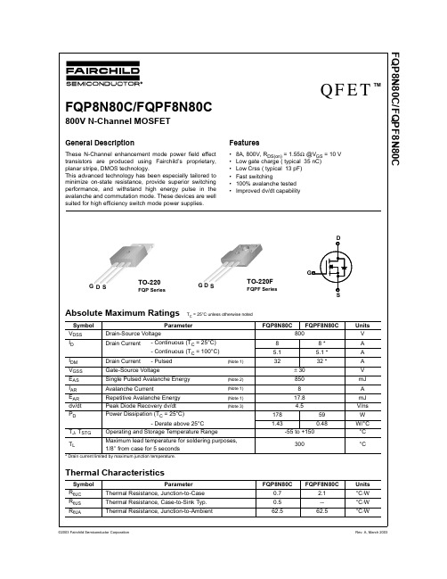
FQP8N80C/FQPF8N80C
FQP8N80C/FQPF8N80C
800V N-Channel MOSFET
QFET TM
General Description
These N-Channel enhancement mode power field effect transistors are produced using Fairchild’s proprietary, planar stripe, DMOS technology. This advanced technology has been especially tailored to minimize on-state resistance, provide superior switching performance, and withstand high energy pulse in the avalanche and commutation mode. These devices are well suited for high efficiency switch mode power supplies.
Features
• 8A, 800V, RDS(on) = 1.55Ω @VGS = 10 V • Low gate charge ( typical 35 nC) • Low Crss ( typical 13 pF) • Fast switching • 100% avalanche tested • Improved dv/dt capability
td(off)
Turn-Off Delay Time
tf
Turn-Off Fall Time
Qg
MSOP10中文资料

MSOP10中⽂资料High EfficiencyWhite LED DriverMonolithic Power SystemsGeneral DescriptionThe MP1521 is a constant-current Boost Regulator. This IC has three individual current-sensing feedbacks, which are ideal for driving multiple strings of series connected LEDs. The OLS pin is designed for detecting loose or open LED connections. The IC uses a peak current, constant minimum off-time architecture. The feedback pins measure voltage across sense resistors in series with the LED strings. When supplying a bias current of 20mA, the voltage drop across the sense resistor is only 0.4V to minimize power loss. Either a DC voltage or a PWM signal at the BRT/PWM input can control the LED brightness.The MP1521 has an on board power MOSFET switch that is protected by current limit, open load shutdown, thermal shutdown, and under voltage lockout .Ordering InformationPart Number ? Package TemperatureMP1521EK MSOP10 -20° to +85°C MP1521EQ QFN16 (3x3) -20° to +85°C EV0005 MP1521EK Evaluation BoardEV0021MP1521EQ Evaluation BoardFor Tape & Reel, add suffix –Z (i.e., MP1521EK–Z) For Lead Free, add suffix –LF (i.e., MP1521EK–LF–Z)FeaturesOn Board Power MOSFETDrive 9 White LEDs from 2.7V Input Drive 15 White LEDs from 5V Input Up to 90% EfficiencyOver 80mA Output Current Capacity Open Load ShutdownLow Current Sensing Feedback Voltage Up to 3 String Current Sensing Feedback Analog and Digital PWM Brightness Control UVLO, Thermal Shutdown Soft StartInternal Current LimitAvailable in Compact MSOP10 and Tiny 3 mm x 3 mm QFN16 Package Evaluation Boards AvailableApplicationsHandheld Computers, Cell phones, PDAs,Digital and Video Cameras, Small LCD DisplaysLi Ion and NiMH Battery ApplicationsTypical Application Circuit (One String of Six (6) LEDs)Efficiency vs LED current, 1 string of 6 Using Toko D62CB 47µH Inductor5060708090100510152025LED Current (mA )E f f i c i e n c y (%)High EfficiencyWhite LED Driver Monolithic Power SystemsAbsolute Maximum Ratings Supply Voltage (V IN ) 28V Switch Voltage to GND -0.5V to 28VV EN , V REF , V BRT , V FB1, V FB2, V FB3 –0.3V to 6V Storage Temperature -55°C to +150°CRecommended Operating ConditionsSupply Voltage (V IN ) 2.7V to 25VOperating Temperature -20°C to +85°C Switch Voltage to GND -0.5V to 25VPackage Thermal CharacteristicsThermal Resistance, ΘJA (MSOP10) 150°C/WThermal Resistance, ΘJA (QFN16) 60°C/W Electrical Characteristics (V IN = 5.0V, T A = 25°C unless specified otherwise) Parameters Symbol Condition Min Typ Max Units Supply Current (shutdown)I IN (OFF) V EN <0.4V 1 3 µA Supply Current (quiescent) I IN (ON) V EN >1.5V, V BRT =0V, V FB =0V 550 700 µA Minimum Off Time, normal operationt OFF (NORMAL) V EN >1.5V, V BRT =0.6VV FB =0400 500 700 nSMinimum Off Time, start-up (Note 1) t OFF (START) V EN >1.5V, V BRT =0.6V,V FB =0V1.52.4 µSUVLOV IN RISING 2.1 2.6 V Under Voltage Lockout V IN FALLING1.92.4 VEnableThreshold 0.8 1.0 2.0 V Hysterisis 60 mV Leakage CurrentV EN =3V 1 µA Open Load Shutdown Threshold Measured at OLS Pin 26 29 V V OLS =15V 1 µALeakage CurrentV OLS =25V 45 70 µAReferenceOutput Voltage I REF =0A 1.20 1.235 1.27 V Load Regulation I REF =0 to 100µA 2.5 5 mV Line Regulation V IN =3 to 15V, I REF =0A 2.5 5 mV Feedback ComparatorThreshold V BRT =1.2V 380 400 420 mV Hysterisis (Note 2) V BRT = 1.2V 30 mV FB Input Bias Current V FB =0.2V -150 -50 0 nA PWM ModeOutput-Off Threshold 0.18 0.26 V BRT Input Bias V BRT =0.6V -100 -30 0 nA BRT Full Scale Threshold(Note 3)1.2 VOutput SwitchSwitch On Resistance (Note 2) R ON V IN =5.0V 0.5 0.6 ? Switch Current Limit 300 400 mA Leakage Current V SW =25V 5 µA Thermal Shutdown (Note 2) 160 °CNotes:1) First 64 pulses after EN switches high. 2) Guaranteed by design.3) The output current is off when BRT is driven below the output-off threshold and full-scale when driven above the full-scale threshold. To PWM the output drive BRT above and below these thresholds.Monolithic Power SystemsPin DescriptionMSOP10 QFN16Part Marking: MP1521EK Part Marking: A1xxTable 1: MP1521 MSOP10 and QFN16 Pin AssignmentsMSOP Pin # QFN Pin# PinName Pin Function 1 16 IN Input supply pin. It can be connected to the regulator’s input supply, or to theoutput for boot-strapped operation (boot-strapped operation is required for V IN ofless than 3V). 2 2 ENRegulator On/Off control input. Logic high (V EN >1V) turns on IC, logic low puts itinto low current shutdown mode. Place a 100K ? resistor in series with EN if it is connected to a voltage greater than 10V.3 4 REF 1.23V reference used for setting the analog control voltage at BRT input. Thisreference can supply up to 200µA to an external load. Do not connect any bypass capacitors to this pin. It is internally compensated.4 5 BRT Analog or PWM input for controlling LED brightness. When used in analogmode, apply a DC voltage of 0.3 to 1.2V. This input voltage is attenuated by 1/3 to set the voltage across sense resistors at FB1, FB2, and FB3. Maximum brightness (20mA) occurs with 1.2V applied. To control brightness in PWM mode, apply a PWM square wave with a minimum voltage less the 0.18V and a maximum greater than 1.2V. When a voltage less than0.18V is applied to this pin, the output switch is turned off. The regulator operates at maximum brightness when more than1.2V is applied. The frequency of the PWM signal must be between 100 to 400 Hz.5 6 7 7 8 9 FB3 FB2 FB1 Feedback input for measuring voltage across current-sense resistor that is in series with LED string. Unused feedback pins must be connected to any used feedback pin. 8 10 OLS Open Load Shutdown pin senses regulator output voltage to protect IC duringopen load operation. When this pin’s voltage exceeds 28V, the output switch is shut off. The output switch remains off until the IC is reset by cycling the enable pin (EN) or input supply (IN) pin.9 11, 12 GND Signal and power ground. Connect directly to ground plane. 10 14 SW Output switch pin, power DMOS low-side switch. - 1, 3, 6,13, 15N/C No Connect SW GND OLS FB1 FB2REF NC EN NC REFGND GND OLS FB1B R TN CF B 3F B 2I NN CS WN CMonolithic Power Systems Figure 2: MP1521 Functional Block DiagramMonolithic Power Systems Functional DescriptionOperationThe MP1521 utilizes a constant off-time control scheme (Refer to the Block Diagram). For maximum brightness, the BRT pin is biased at or above 1.2V. Its voltage is routed through the unity gain buffer whose the output of is clamped at 1.2V. A20K/10K divider from the Buffer to the non-inverting input of the Feedback comparator divides the BRT voltage by three to set the current sense threshold. If any of the feedback pins FB1, FB2, or FB3 is lower than this threshold the Power FET is turned on. The Power MOSFET and inductor current increases until the current limit comparator trips at 0.5A turning off the MOSFET for 500ns. At the end of 500ns if any of the Feedback pins are still lower than the current sense threshold. The Power FET is again turned on. This cycle repeats itself until all three of the feedback pins exceed the threshold.Analog Brightness AdjustAnalog Brightness Adjust is accomplished by applying a voltage between 0.26V to 1.2V on the BRT pin. The 1.23V REF output can be used to bias a potentiometer whose wiper drives the BRT pin. PWM/ Brightness AdjustPWM Brightness Adjust is accomplishedby driving the BRT pin with a square wave whose low voltage is below 0.2V and whose high voltage is greater than 1.2V. A voltage below 0.2V forces the Power MOSFET off. A voltage greater than 1.2V will cause all three feedback pins to regulate at or above 0.4VOpen Load Shut-OffOpen Load Shut-Off is implemented by connecting the OLS pin to V OUT. In the fault condition where the connection to the LED’s is open, V OUT will rise up, as all the feedback pins are absent of voltage. Once V OUT exceeds 28V, the part will cease operation until the EN pin is cycled off and on. To disable the open load shut-off feature, connect the OLS pin to GND.Monolithic Power Systems Application CircuitsFigure 3: One String of Four (4) LEDsMonolithic Power SystemsApplication Circuits ContinuedFigure 5: Two Strings of Four (4) LEDs or Eight (8) LEDs TotalMonolithic Power Systems Package Information MSOP10NOTE:1) Control dimension is in inches. Dimension in bracket is millimeters.QFN16 (3 x 3)Pin 1NOTE:1) Control dimension is in millimeters. Dimension in bracket is inch.NOTICE: MPS believes the information in this document to be accurate and reliable. However, it is subject to change without notice. Please contact the factory for current specifications. No responsibility is assumed by MPS for its use or fit to any application, nor for infringement of patent or other rights of third parties.MP1521 Rev 2.7Monolithic Power Systems, Inc. 8。
f805简明中文手册8p

按钮3-3-2. Selecting Digital Filter按钮,输入你想要的次数。
按3-3-3. Setting Each Code键选择货号。
键切换到定量值设置界面。
通过十个键输入定量值,按面板上一个叫做“这些线必须短接(3) Connecting load cells in parallel 称重传感器的并联方法Some industrial applications require several load cells connected in parallel (e.g., tank or flow scales).A summing junction box should be used to facilitate connection and corner correction.在工业应用中,通常将多个称重传感器并联(如罐秤,流量秤等)。
采用接线盒方便接Register the value of load (balance weight) for calibration.录砝码重量Calibrate the initial zero point.Place the load (balance weight) on the load cell and calibrate the span value.If it is necessary, re-calibrate initial zero point.重新校准零点Disable changing setting value related to calibration.修改与校准有关的参数on the rear panel. (Hardware Lock)换到Release Setting Value Lock which inhibits the calibration.(Software Lock)止校准量程的数值锁解锁(软件封锁)Select Load cell Excitation between 10V and 5V.定在Register the Unit of the scale.Register the position of Decimal Point.Register the maximum capacity of the scale.If the registered value is exceeded by 9 scale divisions, displayshows范围注意:砝码重量必须小于或等于预定承载量,预定承载量必须等于称重传感器承载量。
监控专用8路poe交换机产品说明书
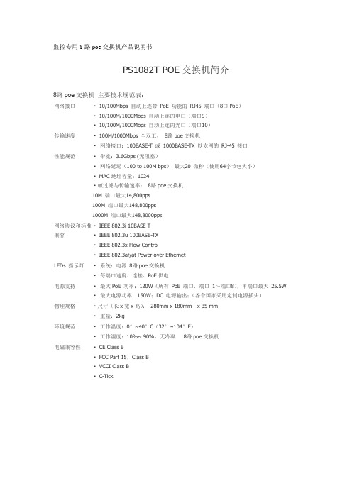
监控专用8路poe交换机产品说明书PS1082T POE交换机简介8路poe交换机主要技术规范表:网络接口· 10/100Mbps 自动上连带PoE 功能的RJ45 端口(8口PoE)· 10/100M/1000Mbps 自动上连的电口(端口9)· 10/100M/1000Mbps 自动上连的光口(端口10)传输速度· 100M/1000Mbps 全双工,8路poe交换机·网络接口:100BASE-T 或1000BASE-TX 以太网的RJ-45 接口性能规范·带宽:3.6Gbps (无阻塞)·网络延迟(100 to 100M bps):最大20 微秒(使用64字节包大小)· MAC地址容量:1024·帧过滤与传输速率:8路poe交换机10M 端口最大14,800pps100M 端口最大148,800pps1000M 端口最大148,8000pps网络协议和标准兼容· IEEE 802.3i 10BASE-T· IEEE 802.3u 100BASE-TX· IEEE 802.3x Flow Control· IEEE 802.3af/at Power over EthernetLEDs 指示灯·系统:电源8路poe交换机·每端口速度、连接、PoE供电电源支持·最大PoE 功率:120W(所有PoE 端口,端口1~端口8),单端口最大25.5W ·最大电源功率:150W;DC 电源输出;(各个国家采用定制电源插头)物理规格·尺寸(长x宽x高):280mm x 180mm x 35 mm·重量:2kg环境规范·工作温度:0°~40°C(32°~104°F)·工作湿度:10%~ 90%,无冷凝8路poe交换机电磁兼容性· CE Class B· FCC Part 15,Class B· VCCI Class B· C-Tick。
FAIRCHILD FQPF17P10 说明书

现货库存、技术资料、百科信息、热点资讯,精彩尽在鼎好!FQPF17P10(Note 4)(Note 4, 5)(Note 4, 5) (Note 4)Notes:1. Repetitive Rating : Pulse width limited by maximum junction temperature2. L = 7.9mH, I AS = -10.5A, V DD = -25V, R G = 25 Ω, Starting T J = 25°C3. I SD ≤ -16.5A, di/dt ≤ 300A/µs, V DD ≤ BV DSS, Starting T J = 25°C4. Pulse Test : Pulse width ≤300µs, Duty cycle ≤2%5. Essentially independent of operating temperature∆BV DSS / ∆T J Breakdown Voltage Temperature CoefficientI D = -250 µA, Referenced to 25°C ---0.1--V/°C I DSS Zero Gate Voltage Drain Current V DS = -100 V, V GS = 0 V -----1µA V DS = -80 V, T C = 150°C -----10µA I GSSF Gate-Body Leakage Current, Forward V GS = -30 V, V DS = 0 V -----100nA I GSSRGate-Body Leakage Current, ReverseV GS = 30 V, V DS = 0 V----100nAOn CharacteristicsV GS(th)Gate Threshold Voltage V DS = V GS , I D = -250 µA -2.0---4.0V R DS(on)Static Drain-Source On-ResistanceV GS = -10 V, I D = -5.25 A --0.140.19Ωg FSForward TransconductanceV DS = -40 V, I D = -5.25 A --8.6--SDynamic CharacteristicsC iss Input Capacitance V DS = -25 V, V GS = 0 V, f = 1.0 MHz--8501100pF C oss Output Capacitance--310400pF C rssReverse Transfer Capacitance--100130pFSwitching Characteristicst d(on)Turn-On Delay Time V DD = -50 V, I D = -16.5 A,R G = 25 Ω--1745ns t r Turn-On Rise Time --200410ns t d(off)Turn-Off Delay Time --45100ns t f Turn-Off Fall Time --100210ns Q g Total Gate Charge V DS = -80 V, I D = -16.5 A,V GS = -10 V--3039nC Q gs Gate-Source Charge -- 4.8--nC Q gdGate-Drain Charge--17--nCDrain-Source Diode Characteristics and Maximum RatingsI S Maximum Continuous Drain-Source Diode Forward Current -----10.5A I SM Maximum Pulsed Drain-Source Diode Forward Current-----42A V SD Drain-Source Diode Forward Voltage V GS = 0 V, I S = -10.5 A -----4.0V t rr Reverse Recovery Time V GS = 0 V, I S = -16.5 A,dI F / dt = 100 A/µs--120--ns Q rrReverse Recovery Charge--0.52--µCDISCLAIMERFAIRCHILD SEMICONDUCTOR RESERVES THE RIGHT TO MAKE CHANGES WITHOUT FURTHER NOTICE TO ANY PRODUCTS HEREIN TO IMPROVE RELIABILITY, FUNCTION OR DESIGN. FAIRCHILD DOES NOT ASSUME ANY LIABILITY ARISING OUT OF THE APPLICATION OR USE OF ANY PRODUCT OR CIRCUIT DESCRIBED HEREIN;NEITHER DOES IT CONVEY ANY LICENSE UNDER ITS PATENT RIGHTS, NOR THE RIGHTS OF OTHERS.LIFE SUPPORT POLICYFAIRCHILD’S PRODUCTS ARE NOT AUTHORIZED FOR USE AS CRITICAL COMPONENTS IN LIFE SUPPORT DEVICES OR SYSTEMS WITHOUT THE EXPRESS WRITTEN APPROVAL OF FAIRCHILD SEMICONDUCTOR CORPORATION.As used herein:1. Life support devices or systems are devices or systems which, (a) are intended for surgical implant into the body,or (b) support or sustain life, or (c) whose failure to perform when properly used in accordance with instructions for use provided in the labeling, can be reasonably expected to result in significant injury to the user.2. A critical component is any component of a life support device or system whose failure to perform can be reasonably expected to cause the failure of the life support device or system, or to affect its safety or effectiveness.PRODUCT STATUS DEFINITIONS Definition of TermsDatasheet Identification Product Status DefinitionAdvance InformationFormative or In Design This datasheet contains the design specifications for product development. Specifications may change in any manner without notice.PreliminaryFirst ProductionThis datasheet contains preliminary data, andsupplementary data will be published at a later date.Fairchild Semiconductor reserves the right to make changes at any time without notice in order to improve design.No Identification Needed Full ProductionThis datasheet contains final specifications. Fairchild Semiconductor reserves the right to make changes at any time without notice in order to improve design.Obsolete Not In ProductionThis datasheet contains specifications on a product that has been discontinued by Fairchild semiconductor.The datasheet is printed for reference information only.TRADEMARKSThe following are registered and unregistered trademarks Fairchild Semiconductor owns or is authorized to use and is not intended to be an exhaustive list of all such trademarks.FACT™FACT Quiet series™FAST ®FASTr™FRFET™GlobalOptoisolator™GTO™HiSeC™I 2C™ImpliedDisconnect™ISOPLANAR™LittleFET™MicroFET™MicroPak™MICROWIRE™MSX™MSXPro™OCX™OCXPro™OPTOLOGIC ®OPTOPLANAR™PACMAN™POP™Power247™PowerTrench ®QFET™QS™QT Optoelectronics™Quiet Series™RapidConfigure™RapidConnect™SILENT SWITCHER ®SMART START™SPM™Stealth™SuperSOT™-3SuperSOT™-6SuperSOT™-8SyncFET™TinyLogic™TruTranslation™UHC™UltraFET ®VCX™ACEx™ActiveArray™Bottomless™CoolFET™CROSSVOLT ™DOME™EcoSPARK™E 2CMOS™EnSigna™Across the board. Around the world.™The Power Franchise™Programmable Active Droop™。
8p环保标准

8p环保标准
8P环保标准是指欧盟对投放于市场的电子和电器设备中的限制,包括邻苯二甲酸盐(PAEs)的8项化合物,分别是:邻苯二甲酸二(2-乙基己基)酯(DEHP)、邻苯二甲酸二丁酯(DBP)、邻苯二甲酸丁基苄酯(BBP)、邻苯二甲酸二异壬酯(DINP)、邻苯二甲酸二异癸酯(DIDP)、邻苯二甲酸二正辛酯(DNOP)、邻苯二甲酸二异己酯(DIHP)和邻苯二甲酸二环己酯(DCHP)。
根据欧盟指令2005/84/EC规定,DEHP、DBP、BBP不得用于儿童玩具用品中,在塑料中每种含量不得超过0.1%;DINP、DIDP、DNOP不得用于能入口的儿童玩具及儿童类物品,每种含量不得超过0.1%。
fqpf8n80c场效应管参数

fqpf8n80c场效应管参数
FQPF8N80C是一种N沟MOS场效应管,其参数如下:
1. 控制阈值电压(Vth):通常为
2.3V至4.0V之间,表示控
制栅极电压和漏源电压之间的临界电压。
2. 静态漏极-源极电阻(Rds(on)):通常为5.8Ω至10.8Ω之间,表示在正常工作条件下,漏极到源极之间的电阻。
3. 最大漏极电流(Id):通常为8A,表示最大允许通过漏极
的电流。
4. 最大漏极-源极电压(Vdss):通常为800V,表示最大允许
的漏极-源极电压。
5. 最大功耗(Pd):通常为125W,表示在最大允许的温度下,管子能够承受的最大功耗。
这些是FQPF8N80C场效应管的一些常见参数,实际数值可能
略有差异,请根据具体的管子参数手册参考。
ProSafe 8-Ports 10 100 1000MB 模块式交换机 GS108P 用户手册说明
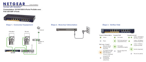
Guide d'installationÉtape 3. Vérifiez l'étatCommutateur 10/100/1000 8-Ports ProSafe avec PoE GS108P 4 Ports GS108PÉtape 2. Branchez l'alimentation Modem en optionÉtape 1. Connectez l'équipementRouteur en optionOrdinateurServeurInternetÉteintAlluméVoyant d'alimentationVoyants de portActivité (clignotant)Pas de lien (éteint)Liaison 1000 Mbits/s (les deux voyants)Liaison 10 Mbits/s (voyant de droite)Liaison 100 Mbits/s (voyant de gauche)Voyants PoEPoE max. VoyantLes ports PoE fonctionnent normalement (désactivés)Le voyant PoE MAX était actif au cours des 2 dernières minutes. (clignotant)PoE utiliséNe pas utiliser PoE (éteint)PoE n'est pas fourni (clignotement lent)PoE arrêté(clignotement rapide)Moins de 7W de puissance PoE disponibleSeptembre 2012Ce symbole a été apposé conformément à la directive européenne 2002/96 sur la mise au rebut des équipements électriques et électroniques (directive WEEE - Waste Electrical and ElectronicEquipment). En cas de mise au rebut de ce produit dans un État membre de l'Union européenne, il doit être traité et recyclé conformément à cette directive.NETGEAR, le logo NETGEAR et Connect with Innovation sont des marques commerciales et/ou des marques déposées de NETGEAR, Inc. et/ou des filiales de NETGEAR aux Etats-Unis et/ou dans d'autres pays. Les informations sont sujettes à changement sans préavis. Les autres marques et noms de produits sont desmarques commerciales ou des marques déposées de leurs détenteurs respectifs. © NETGEAR, Inc. Tous droits réservés.Pour une utilisation en intérieur dans tous les pays de l'UE et la Suisse.Pour consulter la déclaration de conformité complète, rendez-vous sur le site /app/answers/detail/a_id/11621/.Conditions : NETGEAR se réserve le droit d'apporter des modifications aux produits décrits dans ce document sans préavis afin d'en améliorer la conception, les fonctions opérationnelles et/ou la fiabilité. NETGEAR décline toute responsabilité quant aux conséquences de l'utilisation des produits ou des configurations de circuits décrits dans le présent document.SpécificationsSpécification DescriptionInterface réseau Connecteur RJ-45 pour 10BASE-T, 100BASE-TX, ou 1000BASE-TCâble réseau Catégorie 5e (Cat 5e) ou meilleur câble Ethernet Ports8Adaptateur secteur Entrée CC 48V @ 1,25 A Consommation de courant60WBudget d'alimentation PoE 50W max. tous les ports PoE (1-4), 15,4 W max. par port PoE Poids 0,716 kg (1,7 lb)Dimensions (L × P × H)235 mm x 102 mm x 27 mm 9,3 po. x 4,1 po. x 1,1 po.Température de fonctionnement 0-50 ° C (32-122 ° F)Humidité de fonctionnement 10% -90% d'humidité relative, sans condensationConformitéélectromagnétique CE Classe B, FCC Classe B, VCCI Classe B, C-Tick Classe B, CCC Homologations de sécuritéMarquage CE, CB, CCCSupport techniqueAprès l'installation de votre périphérique, notez le numéro de série inscrit surl'étiquette de votre produit. Il vous sera nécessaire pour enregistrer votre produit à l'adresse https:// .Vous devez enregistrer votre produit avant de pouvoir utiliser l'assistancetéléphonique de NETGEAR. NETGEAR vous recommande d'enregistrer votre produit sur le site Web de NETGEAR. Pour obtenir des mises à jour de produits et accéder au support Web, visitez .。
Parker Hannifin PL10胶油器产品说明书
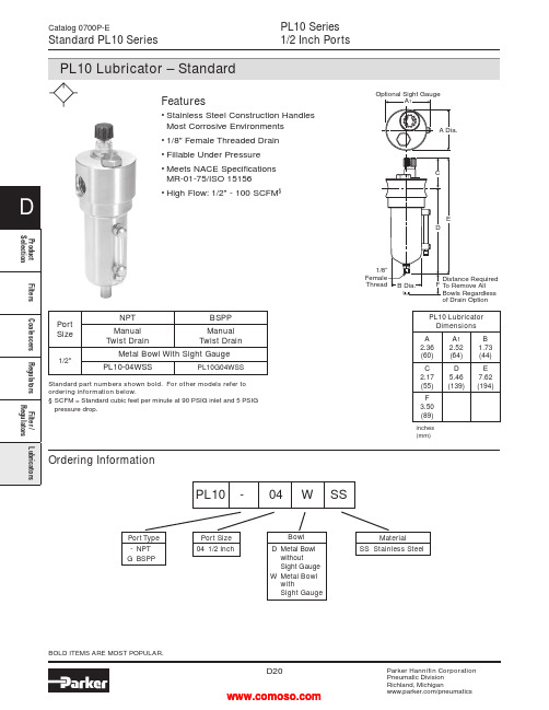
PL10 Series1/2 Inch PortsCatalog 0700P-EStandard PL10 Seriesof Drain Option Ordering InformationPort Type- NPTG BSPPPort Size04 1/2 InchMaterialSS Stainless SteelPL10 - 04 W SSBOLD ITEMS ARE MOST POPULAR.PL10 LubricatorDimensionsA2.36(60)A12.52(64)B1.73(44)C2.17(55)D5.46(139)E7.62(194)F3.50(89)inches(mm)Features• Stainless Steel Construction HandlesMost Corrosive Environments• 1/8" Female Threaded Drain• Fillable Under Pressure• Meets NACE SpecificationsMR-01-75/ISO 15156• High Flow: 1/2" - 100 SCFM§BowlD Metal BowlwithoutSight GaugeW Metal BowlwithSight GaugePortSizeNPT BSPPManualTwist DrainManualTwist Drain1/2"Metal Bowl With Sight GaugePL10-04WSS PL10G04WSSStandard part numbers shown bold. For other models refer toordering information below.§ SCFM = Standard cubic feet per minute at 90 PSIG inlet and 5 PSIGpressure drop.012345P r e s s u r e D r o p - P S I GP r e s s u r e D r o p - b a r.1.2.3Primary Pressure - PSIG1.7 bar3.4 bar 5.2 bar 6.9 barPrimary Pressure - bar051015202530354045Flow - dm /s3nPL10 SeriesAir Line LubricatorsCatalog 0700P-E Technical Specifications – PL10PL10 Filter Kits & AccessoriesDrain Kit –Manual Twist Drain –Small (Old) ..........................................................SA600Y7-1SS Large (New) ...............................................................SAP05481 Pipe Nipple –1/2" 316 Stainless Steel ................................................616A28-SS Sight Dome Kit –(Old)..................................................................................RKL10SS (New) ..................................................................................PS740NSpecificationsBowl Capacity ..................................................................4.0 OuncesPort Threads ..........................................................................1/2 Inch Pressure & Temperature Ratings –Metal Bowl (D) ...................................0 to 300 PSIG (0 to 20.7 bar) 0°F to 150°F (-18°C to 66°C) Metal Bowl (W) ..................................0 to 250 PSIG (0 to 17.2 bar) 0°F to 150°F (-18°C to 66°C)Note: Air must be dry enough to avoid ice formation attemperatures below 32°F (0°C).OperationAir flowing through the unit goes through two paths. At low flow rates the majority of the air flows through the Venturi section (A). The rest of the air opens the check valve (C). The velocity of the air flowing through the Venturi section (A) creates a pressure drop. This lower pressure allows the oil to be forced from the reservoir through the pickup tube (B) and travels up to the metering screw (D). The rate of oil delivery is then controlled by adjusting the metering screw (D). Oil flows past the metering screw (D) and forms a drop in the nozzle tube (E). As the oil drops through the dome (F) and back into the Venturi section (A), it is broken up into fine particles. It is then mixed with the air flowing past the check valve (C) and is carried downstream. As the air flow increases the check valve (C) will open more fully. This additional flow will assure that the oil delivery rate will increase linearly with the increase of air flow.Technical InformationWeight ........................................................................1.9 lb. (0.85 kg)Materials of ConstructionBody .....................................................................316 Stainless Steel Bowl .....................................................................316 Stainless Steel Dip Tube ...............................................................316 Stainless Steel Drain ....................................................................316 Stainless Steel Fill Plug ................................................................316 Stainless Steel Seals .............................................................................Fluorocarbon Sight Dome ...............................................................................Nylon Sight Gauge ........................................................................Isoplast(Revised 11-21-12)Stainless Steel FRLs Catalog 0700P-ENotes。
- 1、下载文档前请自行甄别文档内容的完整性,平台不提供额外的编辑、内容补充、找答案等附加服务。
- 2、"仅部分预览"的文档,不可在线预览部分如存在完整性等问题,可反馈申请退款(可完整预览的文档不适用该条件!)。
- 3、如文档侵犯您的权益,请联系客服反馈,我们会尽快为您处理(人工客服工作时间:9:00-18:30)。
(Note 4)(Note 4, 5)(Note 4, 5) (Note 4)Notes:1. Repetitive Rating : Pulse width limited by maximum junction temperature2. L = 8.0mH, I AS = -5.3A, V DD = -25V, R G = 25 Ω, Starting T J = 25°C3. I SD ≤ -8.0A, di/dt ≤ 300A/µs, V DD ≤ BV DSS, Starting T J = 25°C4. Pulse Test : Pulse width ≤300µs, Duty cycle ≤2%5. Essentially independent of operating temperature∆BV DSS / ∆T J Breakdown Voltage Temperature CoefficientI D = -250 µA, Referenced to 25°C ---0.1--V/°C I DSS Zero Gate Voltage Drain Current V DS = -100 V, V GS = 0 V -----1µA V DS = -80 V, T C = 150°C -----10µA I GSSF Gate-Body Leakage Current, Forward V GS = -30 V, V DS = 0 V -----100nA I GSSRGate-Body Leakage Current, ReverseV GS = 30 V, V DS = 0 V----100nAOn CharacteristicsV GS(th)Gate Threshold Voltage V DS = V GS , I D = -250 µA -2.0---4.0V R DS(on)Static Drain-Source On-ResistanceV GS = -10 V, I D = -2.65 A --0.410.53Ωg FSForward TransconductanceV DS = -40 V, I D = -2.65 A -- 3.9--SDynamic CharacteristicsC iss Input Capacitance V DS = -25 V, V GS = 0 V, f = 1.0 MHz--360470pF C oss Output Capacitance--120155pF C rssReverse Transfer Capacitance--3040pFSwitching Characteristicst d(on)Turn-On Delay Time V DD = -50 V, I D = -8.0 A,R G = 25 Ω--1130ns t r Turn-On Rise Time --110230ns t d(off)Turn-Off Delay Time --2050ns t f Turn-Off Fall Time --3580ns Q g Total Gate Charge V DS = -80 V, I D = -8.0 A,V GS = -10 V--1215nC Q gs Gate-Source Charge -- 3.0--nC Q gdGate-Drain Charge--6.4--nCDrain-Source Diode Characteristics and Maximum RatingsI S Maximum Continuous Drain-Source Diode Forward Current -----5.3A I SM Maximum Pulsed Drain-Source Diode Forward Current-----21.2A V SD Drain-Source Diode Forward Voltage V GS = 0 V, I S = -5.3 A -----4.0V t rr Reverse Recovery Time V GS = 0 V, I S = -8.0 A,dI F / dt = 100 A/µs--98--ns Q rrReverse Recovery Charge--0.35--µCDISCLAIMERFAIRCHILD SEMICONDUCTOR RESERVES THE RIGHT TO MAKE CHANGES WITHOUT FURTHER NOTICE TO ANY PRODUCTS HEREIN TO IMPROVE RELIABILITY, FUNCTION OR DESIGN. FAIRCHILD DOES NOT ASSUME ANY LIABILITY ARISING OUT OF THE APPLICATION OR USE OF ANY PRODUCT OR CIRCUIT DESCRIBED HEREIN;NEITHER DOES IT CONVEY ANY LICENSE UNDER ITS PATENT RIGHTS, NOR THE RIGHTS OF OTHERS.LIFE SUPPORT POLICYFAIRCHILD’S PRODUCTS ARE NOT AUTHORIZED FOR USE AS CRITICAL COMPONENTS IN LIFE SUPPORT DEVICES OR SYSTEMS WITHOUT THE EXPRESS WRITTEN APPROVAL OF FAIRCHILD SEMICONDUCTOR CORPORATION.As used herein:1. Life support devices or systems are devices or systems which, (a) are intended for surgical implant into the body,or (b) support or sustain life, or (c) whose failure to perform when properly used in accordance with instructions for use provided in the labeling, can be reasonably expected to result in significant injury to the user.2. A critical component is any component of a life support device or system whose failure to perform can be reasonably expected to cause the failure of the life support device or system, or to affect its safety or effectiveness.PRODUCT STATUS DEFINITIONS Definition of TermsDatasheet Identification Product Status DefinitionAdvance InformationFormative or In Design This datasheet contains the design specifications for product development. Specifications may change in any manner without notice.PreliminaryFirst ProductionThis datasheet contains preliminary data, andsupplementary data will be published at a later date.Fairchild Semiconductor reserves the right to make changes at any time without notice in order to improve design.No Identification Needed Full ProductionThis datasheet contains final specifications. Fairchild Semiconductor reserves the right to make changes at any time without notice in order to improve design.Obsolete Not In ProductionThis datasheet contains specifications on a product that has been discontinued by Fairchild semiconductor.The datasheet is printed for reference information only.TRADEMARKSThe following are registered and unregistered trademarks Fairchild Semiconductor owns or is authorized to use and is not intended to be an exhaustive list of all such trademarks.FACT™FACT Quiet series™FAST ®FASTr™FRFET™GlobalOptoisolator™GTO™HiSeC™I 2C™ImpliedDisconnect™ISOPLANAR™LittleFET™MicroFET™MicroPak™MICROWIRE™MSX™MSXPro™OCX™OCXPro™OPTOLOGIC ®OPTOPLANAR™PACMAN™POP™Power247™PowerTrench ®QFET™QS™QT Optoelectronics™Quiet Series™RapidConfigure™RapidConnect™SILENT SWITCHER ®SMART START™SPM™Stealth™SuperSOT™-3SuperSOT™-6SuperSOT™-8SyncFET™TinyLogic™TruTranslation™UHC™UltraFET ®VCX™ACEx™ActiveArray™Bottomless™CoolFET™CROSSVOLT ™DOME™EcoSPARK™E 2CMOS™EnSigna™Across the board. Around the world.™The Power Franchise™Programmable Active Droop™。