Self-timed Architecture for Masked Successive Approximation Analog-to-Digital Conversion
基于VR技术的激光三维点云数据的虚拟重建
第42卷第5期 激光杂志Vol.42,No.5 2021 年5 月LASER JOURNAL May,2021基于V R技术的激光三维点云数据的虚拟重建曹贤龙郑州商学院,郑州451200摘要:针对激光扫描云数据的虚拟重建存在噪声大,重建效果差的问题,提出一种激光三维点云数据的 虚拟重建算法。
通过设置多个激光扫描自由度,利用V R技术将激光测量映射到虚拟三维场景当中,获取点云 数据,并利用图像滤波器对采集到的点云数据进行去噪处理。
在此基础上,设置一个主数据点,利用该数据点 对重建激光点云三维数据进行划分,分配重建任务,搜集重建后的结果并显示,完成点云数据的虚拟重建。
实验结果表明,采用改进方法后,噪声被有效剔除,重建效果更佳。
关键词:V R技术;激光扫描;三维点云数据;虚拟重建;数据划分中图分类号:T N249 文献标识码:A doi:10. 14016/ki.jgzz.2021. 05. 205Virtual reconstruction algorithm of laser 3D point cloud dataC A O XianlongZ h e n g zh o u B usin ess U n iv ersity,Z h e n g zh o u451200,C h in aAbstract:Aiming a t the problems of high noise and poor reconstruction effect in the virtual reconstruction of laser scanning cloud data,a virtual reconstruction algorithm of laser3D point cloud data i s proposed.By setting multiple laser scanning degrees of freedom,V R technology i s used t o map the laser measurement t o the virtual three-dimensional scene t o obtain the point cloud data,and the image f i l t e r i s used t o denoise the collected point cloud data.O n this basis,a master data point i s set up t o divide the3D data of laser point cloud that may be reconstructed,distribute the reconstruction task,collect and display the reconstruction results,and complete the virtual reconstruction of the point cloud data.The experimental results show that the noise i s effectively eliminated and the reconstruction effect i s better. Key words:V R technology;laser scanning; 3D point cloud data;virtual reconstruction;data divisioni引言现阶段,以激光成像技术为基础的工业检测以及 逆向工程等行业的兴起,都离不开三维激光扫描成像 技术。
融合注意力和门控空洞卷积的关系识别模型python代码
融合注意力和门控空洞卷积的关系识别模型python代码全文共四篇示例,供读者参考第一篇示例:在深度学习领域,注意力机制和门控卷积是两个被广泛应用的技术。
注意力机制能够帮助模型集中关注于重要的特征,从而提高模型的性能。
而门控卷积则能够有效地捕捉序列数据中的长距离依赖关系。
在本文中,我们将探讨如何将注意力机制和门控卷积结合起来,构建一个用于关系识别的深度学习模型,并使用Python代码实现。
我们需要了解注意力机制和门控卷积的基本原理。
注意力机制是一种用于给予模型不同输入部分不同权重的技术,帮助模型更聚焦于重要的特征。
门控卷积则是一种包含门控单元(如LSTM或GRU)的卷积层,能够在卷积的基础上引入序列建模的能力,捕捉长距离的依赖关系。
接下来,我们将介绍如何将注意力机制和门控卷积结合起来,构建一个关系识别模型。
我们将使用Python编写代码,使用PyTorch作为深度学习框架。
我们需要导入必要的库和模块:```pythonimport torchimport torch.nn as nnimport torch.nn.functional as F```接着,我们定义一个包含注意力机制和门控卷积的关系识别模型:```pythonclass RelationRecognitionModel(nn.Module):def __init__(self, input_dim, hidden_dim, output_dim, num_layers):super(RelationRecognitionModel, self).__init__()self.hidden_dim = hidden_dimself.num_layers = num_layers# 定义门控卷积层self.conv = nn.Conv1d(input_dim, hidden_dim, kernel_size=3, padding=1)# 定义注意力机制self.attention = nn.Linear(hidden_dim, 1)# 定义LSTM层self.lstm = nn.LSTM(hidden_dim, hidden_dim, num_layers, batch_first=True)# 定义输出层self.fc = nn.Linear(hidden_dim, output_dim)def forward(self, x):# 进行卷积操作x = F.relu(self.conv(x))# 计算注意力权重attention_weights = F.softmax(self.attention(x), dim=1)# 将注意力权重应用到卷积结果上x = x * attention_weights# 将数据输入到LSTM层h0 = torch.zeros(self.num_layers, x.size(0),self.hidden_dim).to(x.device)c0 = torch.zeros(self.num_layers, x.size(0),self.hidden_dim).to(x.device)out, _ = self.lstm(x, (h0, c0))# 获取LSTM输出的最后一个时间步的结果,并输入到全连接层out = self.fc(out[:, -1, :])return out```在上面的代码中,我们首先定义了一个包含门控卷积、注意力机制、LSTM和全连接层的关系识别模型。
ssti 模板注入 重庆橙子 解题
SSTI(Server Side Template Injection)是一种常见的Web安全漏洞,它允许攻击者向应用程序中的模板引擎注入恶意代码,从而执行任意的服务器端代码。
在本文中,我们将介绍SSTI的工作原理、危害和防范方法,并结合重庆橙子解题的案例来深入探讨该漏洞的具体应用与解决方案。
一、SSTI的工作原理SSTI漏洞通常出现在使用模板引擎的Web应用程序中,比如Jinja2、Smarty、Twig等。
这些模板引擎在渲染页面时,会将用户提供的参数插入到模板中,如果未对用户输入做出恰当的过滤和验证,就可能导致SSTI漏洞的产生。
攻击者可以通过构造恶意的输入,将恶意代码注入到模板中,从而执行服务器端的任意代码,进而获取服务器的敏感信息、控制服务器等。
二、SSTI的危害SSTI漏洞的危害相当严重,一旦被攻击者利用,可能会对Web应用程序造成以下危害:1. 服务器的敏感信息泄露:攻击者可以利用SSTI漏洞来获取服务器的敏感信息,比如数据库连接信息、操作系统信息等,从而为后续的攻击行为做准备。
2. 服务器端代码的执行:攻击者可以通过SSTI漏洞执行服务器端的任意代码,比如上传恶意文件、获取系统权限等,从而对服务器进行控制。
3. 用户的隐私数据泄露:攻击者可以通过SSTI漏洞,获取用户在Web应用程序中输入的敏感信息,比如个人资料、银行卡号等,从而侵犯用户的隐私。
三、SSTI的防范方法为了防范SSTI漏洞的产生,我们可以采取以下措施:1. 输入验证与过滤:对用户输入的数据进行严格的验证和过滤,确保用户输入的数据符合预期的格式和内容。
2. 模板引擎的安全配置:在使用模板引擎时,确保对其进行安全配置,禁止执行隐式转换、对用户输入进行适当的过滤等操作。
3. 输出编码:在将用户输入的数据输出到模板中时,应该进行适当的编码,避免恶意输入被直接执行。
四、重庆橙子解题案例重庆橙子解题是一家知名的网络安全公司,他们在日常的渗透测试中发现了多个SSTI漏洞,并成功地利用这些漏洞进行了攻击。
modeltime包的用法

modeltime包的用法ModelTime是一个Python包,用于时间序列模型的建模和预测。
它提供了一系列的时间序列模型,包括常见的ARIMA模型、GARCH模型、VAR模型等。
此外,ModelTime还提供了一些用于时间序列预处理和特征工程的功能,如季节性分解、平稳性检验等。
本文将详细介绍ModelTime包的使用方法,并通过案例演示如何进行时间序列的建模和预测。
一、安装和导入ModelTime包首先,我们需要安装ModelTime包。
可以通过pip命令来进行安装:pip install ModelTime安装完成后,就可以通过import语句导入ModelTime包了:import ModelTime as mt二、时间序列数据的读取和预处理在进行时间序列模型建模之前,我们需要先读取数据,并对数据进行预处理。
1.读取数据读取时间序列数据可以使用pandas包中的read_csv函数。
假设我们有一个名为data.csv的文件,其中包含了时间序列数据。
可以通过以下代码将数据读取到DataFrame中:import pandas as pddata = pd.read_csv('data.csv')2.转换为时间序列将读取到的数据转换为时间序列数据,可以使用pandas中的to_datetime函数。
假设我们的数据中有一个列名为'date',表示时间。
我们可以通过以下代码将其转换为时间序列数据:data['date'] = pd.to_datetime(data['date'])3.设置时间为索引为了方便进行时间序列的处理和建模,我们需要将时间列设置为数据的索引。
可以使用pandas中的set_index函数来完成这一步骤:data.set_index('date', inplace=True)4.平稳性检验对于时间序列模型,通常要求数据是平稳的。
纹理物体缺陷的视觉检测算法研究--优秀毕业论文
摘 要
在竞争激烈的工业自动化生产过程中,机器视觉对产品质量的把关起着举足 轻重的作用,机器视觉在缺陷检测技术方面的应用也逐渐普遍起来。与常规的检 测技术相比,自动化的视觉检测系统更加经济、快捷、高效与 安全。纹理物体在 工业生产中广泛存在,像用于半导体装配和封装底板和发光二极管,现代 化电子 系统中的印制电路板,以及纺织行业中的布匹和织物等都可认为是含有纹理特征 的物体。本论文主要致力于纹理物体的缺陷检测技术研究,为纹理物体的自动化 检测提供高效而可靠的检测算法。 纹理是描述图像内容的重要特征,纹理分析也已经被成功的应用与纹理分割 和纹理分类当中。本研究提出了一种基于纹理分析技术和参考比较方式的缺陷检 测算法。这种算法能容忍物体变形引起的图像配准误差,对纹理的影响也具有鲁 棒性。本算法旨在为检测出的缺陷区域提供丰富而重要的物理意义,如缺陷区域 的大小、形状、亮度对比度及空间分布等。同时,在参考图像可行的情况下,本 算法可用于同质纹理物体和非同质纹理物体的检测,对非纹理物体 的检测也可取 得不错的效果。 在整个检测过程中,我们采用了可调控金字塔的纹理分析和重构技术。与传 统的小波纹理分析技术不同,我们在小波域中加入处理物体变形和纹理影响的容 忍度控制算法,来实现容忍物体变形和对纹理影响鲁棒的目的。最后可调控金字 塔的重构保证了缺陷区域物理意义恢复的准确性。实验阶段,我们检测了一系列 具有实际应用价值的图像。实验结果表明 本文提出的纹理物体缺陷检测算法具有 高效性和易于实现性。 关键字: 缺陷检测;纹理;物体变形;可调控金字塔;重构
Keywords: defect detection, texture, object distortion, steerable pyramid, reconstruction
II
dreambooth微调原理

dreambooth微调原理Dreambooth 是 OpenAI 团队为GPT-3.5 语言模型提供的一种微调方法。
微调是指在模型已经通过大规模的预训练阶段获得通用语言理解能力后,使用特定领域的数据进行进一步训练,以适应该领域的任务或需求。
Dreambooth 的微调原理可以概括如下:1. 数据收集:首先,OpenAI 团队会收集与目标任务相关的数据。
对于Dreambooth 来说,它需要进行对话和回答问题,因此需要收集相关的对话和问答数据。
2. 任务定义:在微调之前,需要明确具体的任务要求和目标。
这可能包括确定对话系统的行为规则、优化回答质量等。
3. 损失函数设计:为了使模型能够根据任务需求进行微调,需要设计合适的损失函数。
损失函数用于衡量模型在特定任务上的性能,并通过最小化损失来优化模型的参数。
4. 微调训练:接下来,在收集到的数据上进行模型的微调训练。
训练过程中,通过反向传播算法和梯度下降等技术,根据损失函数更新模型的权重参数,使其在目标任务上表现更好。
5. 超参数调优:微调过程中还需要对一些超参数进行调优,例如学习率、批量大小等。
这些超参数的选择可能会对微调结果产生影响,因此需要通过实验和验证来选择最优的超参数组合。
6. 评估和迭代:在微调训练完成后,需要对模型进行评估和调优。
通过与人工标注或其他基准系统进行对比,评估模型在特定任务上的性能,并根据评估结果进行迭代改进。
Dreambooth 使用这样的微调过程,利用采集的与对话和问答相关的数据,针对特定的对话和问答任务进行模型微调。
这样可以使模型更好地适应目标任务的需求,并提升模型在特定任务上的表现。
Python与Hootsuite自动化社交媒体管理

Python与Hootsuite自动化社交媒体管理在当今数字化的时代,社交媒体已经成为企业和个人推广品牌、与受众互动以及获取信息的重要渠道。
然而,管理多个社交媒体平台可能是一项繁琐且耗时的任务。
这就是为什么自动化工具变得如此重要,而 Python 和 Hootsuite 的结合为我们提供了强大的解决方案。
Python 作为一种强大的编程语言,具有广泛的应用领域,包括数据科学、机器学习、Web 开发等等。
在社交媒体管理方面,Python 可以发挥其优势,帮助我们实现各种自动化任务。
首先,Python 可以用于数据收集和分析。
通过使用相关的库,如`requests` 和`BeautifulSoup`,我们能够从社交媒体平台上抓取数据,例如用户的评论、点赞数、分享数等。
这些数据可以为我们提供有关受众行为和兴趣的有价值洞察,从而帮助我们制定更有效的社交媒体策略。
其次,Python 能够实现内容的自动化生成。
借助自然语言处理库,如`NLTK` 和`SpaCy`,我们可以根据给定的主题或关键词生成吸引人的文案。
这不仅节省了时间,还确保了内容的一致性和质量。
再者,Python 可以用于自动化的社交媒体发布。
我们可以编写脚本,将预先准备好的内容按照预定的时间和频率发布到不同的社交媒体平台上,确保我们的信息能够及时传达给受众。
Hootsuite 则是一款知名的社交媒体管理平台,它集成了多个社交媒体渠道,如 Facebook、Twitter、Instagram 等,为用户提供了一个集中管理的界面。
Hootsuite 的主要优势之一是其强大的调度功能。
用户可以轻松安排帖子的发布时间,确保在最佳的时间段与受众互动。
此外,它还提供了监控和分析工具,让我们能够实时跟踪帖子的表现,了解哪些内容最受欢迎,哪些需要改进。
当 Python 与 Hootsuite 结合使用时,其效果更是显著。
我们可以使用 Python 编写脚本来与 Hootsuite 的 API 进行交互,实现更高级的自动化功能。
Adobe Acrobat SDK 开发者指南说明书

This guide is governed by the Adobe Acrobat SDK License Agreement and may be used or copied only in accordance with the terms of this agreement. Except as permitted by any such agreement, no part of this guide may be reproduced, stored in a retrieval system, or transmitted, in any form or by any means, electronic, mechanical, recording, or otherwise, without the prior written permission of Adobe. Please note that the content in this guide is protected under copyright law.
Synopsys Platform Architect系统级分析和优化说明书
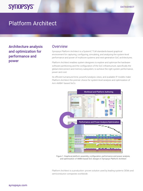
DATASHEETOverview Synopsys Platform Architect is a SystemC TLM standards-based graphical environment for capturing, configuring, simulating, and analyzing the system-level performance and power of multicore systems and next-generation SoC architectures.Platform Architect enables system designers to explore and optimize the hardware-software partitioning and the configuration of the SoC infrastructure, specifically the global interconnect and memory subsystem, to achieve the right system performance, power and cost.Its efficient turnaround time, powerful analysis views, and available IP models make Platform Architect the premier choice for system-level analysis and optimization of Arm AMBA®-based SoCs.Workload and Platform Authoring Architecture analysisand optimization forperformance andpowerPlatform ArchitectPlatform Architect is a production- proven solution used by leading systems OEMs and semiconductor companies worldwide.Highlights• Address the architecture challenges of Artificial Intelligence (AI)-enabled SoCs and multi-chip systems• Hardware-software partitioning and optimization of multicore systems• SoC interconnect and memory subsystem performance and power optimization• Efficient exploration using traffic generation and cycle-accurate TLM interconnect models• Unified view of activity, performance and power for root-cause analysis• Parameter sweeping and sensitivity analysis• Hardware-software validation using cycle-accurate TLM processor models• Compliant with IEEE 1666-2011 SystemC and TLM-2.0 as well as IEEE 1804 UPF 3.0 for system level power analysis Problem: Predicting System Performance and PowerPredicting the dynamic system performance and power of today’s multi-function, multi-application SoCs requires simulation.This impacts both system OEMs and semiconductor companies, and creates an opportunity for information sharing and collaboration within the supply chain.Challenges with Traditional MethodsDiscovering problems with system performance and power consumption late in the development cycle can be catastrophic to project schedules and product competitiveness, causing failure in the market. Accurate architecture analysis must be done earlier in the design cycle:• While spreadsheets are good for aggregating data, static spreadsheet calculations are not accurate enough to estimate performance and power and make design decisions. Dynamic simulation is needed.• Traditional RTL simulation is too slow and lacks the configurability and visibility to analyze performance. In addition,the RTL may simply not be available• Risks include over-design, under-design, cost increases, schedule delays, and re-spinsSolution: Dynamic System-Level Architecture Simulation and AnalysisSynopsys Platform Architect provides system designers with the dynamic transaction-level simulation of performance and power, rapid turnaround time, and powerful system-level visibility they need to greatly improve the analysis and decision-making process. Address the Architecture Challenges of AI SoCs and Multi-Chip SystemsEasily map AI workloads to different SoC architectures to resolve AI power and performance design challenges with Platform Architect. Quickly address challenges of evolving algorithms, highly parallel compute and high memory requirements, with• A library of configurable AI operators for modeling Convolutional Neural Networks (CNNs)• Automated import of workloads from AI frameworks via prototxt and ONNX• An example NVDLA performance model to rapidly represent custom AI acceleratorsAI Operator library CNN workload modelFigure 2: AI Exploration Pack for performance analysis of AI accelerators Hardware-Software Partitioning and Optimization of Multicore Systems Platform Architect enables architects to create task-based workload models of the end-product application for early architecture analysis.Product trends requiring analysis Dynamic workloads generated by multiple initiators and software stacks Highest processing and memory bandwidth requirements by AI applicationsComplex interconnect topologies with hierarchical arbitration and advanced QoS capabilitiesComplex memory hierarchies with caches, on-chip SRAM, off-chip DDRResults with Platform Architect Quantitative analysis results on Key Performance Indicators like effective operations per second, frame-rate, etc. Fast turn-around time for architectural 'what-if' experimentsMeasurable improvement in product performance and powerReduced schedule risk vs. traditional RTL-based methodsFigure 3: SoC performance analysis challenges and the benefits of using system-levelmethods for performance and power analysis in Synopsys Platform ArchitectGeneric task models are easily configured to create a SystemC performance model of the application, called a task-graph.• Using a task-graph, the performance workload of parallel application tasks are mapped onto Virtual Processing Unit (VPU) task-driven traffic generators• Simulation and task analysis enables hardware/software partitioning to be optimized for best system performanceand power well before the application software is available• Task graphs also model the traffic generated by the initiators enabling performance optimization of the interconnect and memory subsystem• Platform Architect includes a Task Graph Generator (TGG) tool that generates application task graphs from sofware execution traces, like VDK software analysis, Linux ftrace, Android atrace, or QNX kernel trace. The TGG can be customized to generate task graphs from custom software trace formats.Interconnect and Memory Subsystem Performance Optimization Using Synthetic and Trace-Driven Traffic GenerationPlatform Architect focuses on architecture design challenges associated with the optimization and performance validation of the backbone SoC interconnect and global memory subsystem:• Dynamic application workloads are modeled using traffic generation, enabling early measurement of system performance and power before software is available• Simulation sweeping enables analysis data to be collected parametrically, exploring all traffic scenarios against a wide range of architecture configurations• Powerful tools for analysis visualization provide graphical transaction tracing and statistical analysis views that enable identification of performance and power bottlenecks, determine their root-cause, and examine the sensitivity that system performance may have to individual or combined parameter settingsThe result is an executable specification used to carefully dimension the SoC interconnect and memory subsystem to support the latency, bandwidth, and power requirements of all relevant SoC components, under all operating conditions.Hardware/Software Performance Validation Using Processor Modelsand Critical SoftwareAfter exploration, the model of the candidate architecture can be refined to replace the task-based workload model with cycle- accurate processor models. This enables architects to validate the architecture candidate using the available performance critical software.Software and hardware analysis views can be visualized together to provide unique system-level visibility to measure performanceand power, and to confirm goals are met.Complete IEEE 1666-2011 SystemC TLM-2.0 Standards-Based EnvironmentSynopsys Platform Architect is a SystemC-based environment fully compatible with the IEEE 1666-2011 SystemC and TLM-2.0 Language Reference Manual (LRM). It supports the assembly, simulation and analysis of models containing mixed levels of abstraction, including:• Standards-based SystemC transaction-level models using IEEE 1666-2011 TLM-2.0 and Accellera Systems Initiative (ASI) TLM industry standards, and the open Synopsys SystemC Modeling Library (SCML) API library for highly reusable TLM-2.0 based peripheral modeling• Support for the IEEE 1804 UPF standard for the creation of system level power models. These can be connected to the TLM performance models to analyze the system-level power consumption based on dynamic activity.• M ixed SystemC/HDL co-simulation with Synopsys VCS and other third-party HDL simulation environments enabling reuse of RTL memory controllers and other IP components• A n Eclipse-based Integrated Development Environment for development and integration of SystemC based models, including a TLM Creation perspective for development and testing of SCML-based peripheral models and custom task models, as well as a TLM Debug perspective for SystemC aware source code debugging, tracing and analysisGetting Started with Available Architecture IP ModelsPlatform Architect supports the broadest commercially available portfolio of pre-instrumented SystemC TLM IP models for architecture exploration and validation.Task-based and Software-based Workload Modeling• G eneric Virtual Processing Units (VPUs) for application task-mapping with synthetic and trace-based traffic generation• Cycle-accurate SystemC-based TLM Arm Cycle Models, ARC nSim/nCam and xCAM models, Tensilica and MIPS processor families, and HDL co-simulation with user-provided RTL for other processor families• Accurate performance models of the DesignWare Embedded Vision (EV) subsystem, including nSim/nCAM model of the ARC Vector processor and the Fast Performance Model (FPM) of the Deep Neural Network (DNN) acceleratorInterconnect Models• Generic, fast, approximately-timed SystemC TLM models for AMBA-based coherent and non-coherent interconnect andnetwork-on-chip• Integration of architecture models for the Arteris FlexNoC™ Network on Chip (NoC) interconnect• C ycle-accurate SystemC TLM bus libraries for Arm CoreLink™ Network Interconnect and Synopsys DesignWare IPAXI interconnect• I ntegration of Arm Cycle Models for implementation accurate interconnect models of Arm coherent and non-coherent interconnects• F low for integration of 3rd-party interconnect models for full configurability in Platform Architect• G eneric configurable models of chip-to-chip protocols for PCIe and EthernetMemory Controller Models• Accurate SystemC TLM performance models of Synopsys DesignWare DDR memory controllers, including the DDR5/4 controller, the DDR5/4/4X controller and the enhanced Universal DDR Memory Controller (uMCTL2)• Generic approximately-timed SystemC TLM multi-port memory subsystem models for Arm AXI and CHI protocols• Cycle-accurate memory subsystem models through HDL co-simulation with user-provided, third-party, and Synopsys RTL memory controller IPProcessor Models• Cycle-accurate SystemC TLM processor support packages (PSPs) for Tensilica and MIPS processor families, and through HDL co-simulation with user-provided RTL for Arm processor familiesCoStart Enablement ServicesSynopsys CoStart is a packaged service that shortens the ramp-up cycle for architecture design methodologies so that users become productive in the shortest time.The Synopsys CoStart program contains an intense knowledge transfer, while assisting in architecture study project planning, use case traffic capture, architecture model creation, simulation, and analysis of results:• Tool, IP model, and methodology training that ensures end-user value at each step, accelerating results• Modeling services for the development and integration of custom interconnect and memory subsystem models, minimizing the modeling effort to get started and achieve initial value• Expert consulting and support to maximize ROI through exploration (not just checking)About Synopsys Virtual Prototyping SolutionsPlatform Architect is part of Synopsys’ comprehensive Virtual Prototyping solution offering that:• Provides the broadest portfolio of system-level IP models from a single supplier• Accelerates the creation and optimization of common SoC blocks• Facilitates SoC architecture exploration and optimization• Provides the most complete prototyping solutions to accelerate embedded software development and system validation• Includes comprehensive training materials and examples• Enables value throughout the semiconductor supply chainFor more information on Platform Architect visit: /platformarchitect©2021 Synopsys, Inc. All rights reserved. Synopsys is a trademark of Synopsys, Inc. in the United States and other countries. A list of Synopsys trademarks isavailable at /copyright.html . All other names mentioned herein are trademarks or registered trademarks of their respective owners.。
输电线路杆塔空气间隙三维可视化管理系统

输电线路杆塔空气间隙三维可视化管理系统许焱1,郭宁1,张辉1,苗堃1,李超1,刘亚文2*(1.国网河南省电力公司济源供电公司,河南济源459000;2.武汉大学遥感信息工程学院,湖北武汉430079)摘要:在Web GIS 框架下构建了真三维场景的防风偏参数杆塔空气间隙管理系统,提出了兼顾数据量和表现力的无人机摄影测量输电线路建模方案,保证了三维场景的精细度与可量测性,并设计了合理的系统多源数据组织方式及数据浏览、查询、分析等功能。
实践表明,该系统能够实现在真实三维场景下,对杆塔空气间隙的查看、浏览与分析,为输电线路防风偏提供有效的分析平台。
关键词:杆塔空气间隙;可视化管理系统;输电线路点云模型中图分类号:P208文献标志码:B文章编号:1672-4623(2022)04-0163-05doi:10.3969/j.issn.1672-4623.2022.04.035Transmission Line Tower-line Air Gap Management SystemBased on 3D Visualization SceneXU Yan 1,GUO Ning 1,ZHANG Hui 1,MIAO Kun 1,LI Chao 1,LIU Yawen 2(1.State Grid Henan Jiyuan Electric Power Supply Company,Jiyuan 459000,China;2.School of Remote Sensingand Information Engineering,Wuhan University,Wuhan 430079,China)Abstract:The tower-line air gap management system with real 3D scene based on Web GIS was constructed.This paper presented a transmis-sion line modeling scheme on UA V photogrammetry that ensures 3D scene precision and measurability.A reasonable multi-source data organiza-tion and data browsing,query and analysis functions were designed for this management system.The practice shows that this management sys-tem can achieve tower-line air gap query,browse and analysis in real 3D scene,and provide a reliable analysis platform for transmission line windage yaw prevention.Key words:tower-line air gap,management system on 3D visualization scene,transmission line point model随着通信技术、网络技术的广泛应用,结合Web GIS 和虚拟建模技术的输电线路管理系统成为主流,如文献[1]将三维仿真场景同日常输电线路管理结合起来,实现电网企业智能化的运行和管理。
facial_landmarks_idxs的常见用法

FACIAL_LANDMARKS_IDXS是一个有序字典,用于存储人脸特征点的索引。
这些特征点通常用于人脸识别和表情分析。
在人脸识别中,通过检测人脸的特征点位置,可以确定人脸的姿态、表情和形状等重要信息。
在dlib库中,使用FACIAL_LANDMARKS_IDXS可以提取人脸特征点。
该库使用68个点来包围每个部位,例如,第37个点到第42个点代表右眼,在图片上这几个点若显示出来就是把右眼那块区域包围着。
通过这些点之间距离的变化可以判断人脸的变化,比如是否眨眼等操作。
在具体使用中,首先需要将人脸检测器和人脸关键点检测器进行训练。
然后可以使用检测器在图像或视频帧上找到人脸并提取出特征点。
这些特征点可以用于人脸识别、表情分析、姿态估计等任务。
此外,还可以将提取的特征点用于人脸识别和验证。
通过比较两张人脸的特征点,可以确定它们是否匹配,从而验证身份。
总之,FACIAL_LANDMARKS_IDXS是一个用于人脸特征点提取的有序字典,可以在人脸识别、表情分析、姿态估计等任务中使用。
【小型微型计算机系统】_设计方法_期刊发文热词逐年推荐_20140723

2009年 序号 1 2 3 4 5 6 7 8 9 10 11 12 13 14 15 16 17 18 19 20 21 22 23 24 25 26 27 28 29 30 31 32 33 34 35 36 37 38 39 40 41 42 43 44 45
46 47 48 49 50 51 52 53 54 55 56 57 58 59 60 61 62 63 64 65 66 67 68 69 70 71 72 73 74 75 76 77 78 79 80 81 82 83 务 保密通信 体系结构描述语言 体系结构 传感器网络结点 会话初始化协议 优化设计 二义性 中心检测 不确定性 不尽相异元素 一致性策略 webit vlsi t.38终端 ssfnet soc sip性能测试 sip协议测试 sip sd总线 r可重排列 rsa 加密/解密 radix-8booth译码 orgmas tool orgmas montgomery模乘 monte carlo minicore melp mandelbrot集 linux运行环境 julia集 ip传真 gpio模拟 fpga实现 dtd agent
2008年 序号 1 2 3 4 5 6 7 8 9 10 11 12 13 14 15 16 17 18 19 20 21 22 23 24 25 26 27 28 29 30 31 32 33 34 35 36 37 38 39 40 41 42 43 44 45
科研热词 推荐指数 负载均衡 2 智能网络磁盘集群存储系统(indcss) 2 智能i/o调度 2 安全协议 2 xml 2 farp表 2 鲁棒优化 1 非线性方程组 1 非线性动态系统 1 非线性函数 1 非形式化分析 1 静态分析 1 门限方案 1 遗传算法 1 逻辑化简 1 适用性 1 边界检测 1 资源映射 1 贪心算法 1 误报率 1 语音压缩编码 1 解码 1 覆盖组播 1 补偿 1 节能 1 自适应 1 背对背 1 网络路由 1 网络安全 1 网络处理器 1 网格应用程序 1 缓存结构 1 维纳模型 1 结构化比较 1 组织 1 线性表 1 纠删编码 1 索引 1 系数规范化 1 粗糙集 1 算法复杂度 1 简化决策表 1 移动传感器网络定位 1 离散混沌加密 1 神经网络 1
spyglass-高级lint-check

Richest set of built-in syntax checks2350+ built-in rules for Verilog, VHDL, V2K, SystemVerilog and mixed languageLint, Openmore, Morelint standards575+ lint, coding style, IP-reuse rulesSTARC, STARC2002, STARCAD21, STARC 2005Recognized industry standard rules from consortium of top 11 semiconductor companies in Japan500+ rules for best practices, coding guidelines, IP-reuse, etc.
Source: I.B.S. Inc.
Source: Gartner
SoC Development Cost
Typical Impact Of Poorly Coded RTL
Chip killer bugs/escapesFixing the problems late in design cycle delays scheduleCombinational loops, non tri-state nets cause functional failureIncorrect FSM behavior causes functional failureLong time to complete verificationIncomplete coverage - Only as complete as your set of simulation vectorsCreating test vectors/assertions is time-consuming and complexSynthesis/simulation mismatch, incomplete initialization cause verification delaysPoor area, power, testability and timing of the chipUnintended redundant logic, use of complex FSM’s lead to poor QoRNo predictability in the design process to hit the market windowDesign reviews are manual, ad-hoc and subjectiveA chip company identified 10+ structural issues that would take 2 to 4 days each to identify and fix in the normal implementation flow
信息茧房封闭自我作文

信息茧房封闭自我作文英文回答:An echo chamber is a metaphorical room where only one's own ideas and beliefs are amplified and reinforced. It is a self-perpetuating cycle that can lead to a distorted view of reality and a lack of critical thinking.Social media has become a major contributor to the formation of echo chambers. Algorithms and user-generated content create personalized experiences that reinforce existing biases and limit exposure to alternative viewpoints. This insular environment can lead to a false sense of consensus and make it difficult to engage in meaningful dialogue with those who hold different beliefs.The consequences of echo chambers are far-reaching. They can contribute to political polarization, misinformation, and a lack of empathy. Individuals who spend too much time in echo chambers may become lesstolerant of dissenting opinions and more likely to engagein extreme behavior.Breaking out of an echo chamber requires conscious effort. It involves seeking out information from diverse sources, engaging with people who have different viewpoints, and being willing to challenge one's own beliefs. It is not always easy, but it is essential for maintaining a healthy and well-informed perspective.中文回答:信息茧房的自我封闭。
python凯撒密码maketrans函数

Python中有一个很有用的函数叫做maketrans,它可以帮助我们快速地实现凯撒密码的加密和解密。
凯撒密码是一种简单的替换加密方法,它是通过将明文中的每个字母按照一个固定数目进行偏移来加密信息的。
maketrans函数可以用来创建一个转换表,通过这个表我们就可以很方便地进行加密和解密操作。
1. maketrans函数的基本用法maketrans函数是Python中字符串对象的一个方法,它的基本用法如下:```pythonstr.maketrans(intab, outtab)```其中,intab是一个包含需要替换的字符的字符串,outtab是一个包含替换字符的字符串。
它返回一个转换表,这个转换表可以被用于str.translate方法,从而实现字符转换的功能。
2. 凯撒密码的加密下面,我们通过maketrans函数来实现凯撒密码的加密操作。
假设我们需要对明文进行一个偏移量为3的加密,代码如下:```pythonimport stringdef caesar_encrypt(text, shift):alphabet = string.ascii_lowercaseshifted_alphabet = alphabet[shift:] + alphabet[:shift]table = str.maketrans(alphabet, shifted_alphabet)return text.translate(table)pl本人ntext = "hello"ciphertext = caesar_encrypt(pl本人ntext, 3)print(ciphertext) #输出: khoor```在这段代码中,我们首先定义了一个caesar_encrypt函数,它接受两个参数,分别是明文和偏移量。
我们创建了一个转换表,并将其用于text.translate方法,从而实现了对明文的加密操作。
refinemask原理

refinemask原理RefineMask是一种图像处理技术,用于精细化掩模的生成和图像分割。
它通过对图像中的对象进行分割,将目标对象与背景区分开来,从而实现对图像的精确处理。
RefineMask的原理基于深度学习模型,该模型通过训练大量的图像数据,学习到了对象的特征和边界信息。
它可以根据输入图像中的像素值,预测每个像素属于前景还是背景。
通过对预测结果进行迭代优化,RefineMask能够逐渐提升分割的准确性和精细度。
在RefineMask的处理过程中,首先需要对输入图像进行预处理,包括图像的缩放、归一化等操作。
然后,将预处理后的图像输入到深度学习模型中进行分割。
模型会输出一个掩模,这个掩模表示图像中每个像素的前景或背景信息。
为了提高分割的准确性,RefineMask还引入了迭代优化的机制。
在每一轮迭代中,模型会根据当前的分割结果和真实标签进行比较,计算损失函数,并利用反向传播算法对模型参数进行更新。
通过多轮迭代,RefineMask能够逐渐提升分割的精确度,使得分割结果更加准确。
RefineMask在图像处理领域有着广泛的应用。
例如,在图像编辑中,可以使用RefineMask对图像中的对象进行提取,从而实现背景替换、图像合成等效果。
在计算机视觉领域,RefineMask可以用于目标检测和目标跟踪,帮助机器识别和理解图像中的对象。
总的来说,RefineMask是一种基于深度学习的图像分割技术,通过对图像中的对象进行精确的分割,实现对图像的精细化处理。
它具有广泛的应用前景,并在图像处理领域发挥着重要的作用。
通过不断优化和改进,RefineMask有望在未来实现更加精确和高效的图像分割效果。
python aes模块的解释 -回复
python aes模块的解释-回复Python AES模块的解释在密码学中,高级加密标准(Advanced Encryption Standard,AES)是一种对称密钥加密算法,被广泛应用于保护敏感数据的安全传输和存储。
Python中的AES模块是专门用于实现AES算法的库。
本文将一步一步回答以下主题:如何安装AES模块、AES模块的基本功能、使用AES模块进行加密和解密的步骤、AES模块的常见应用场景以及AES模块的优缺点。
一、如何安装AES模块要使用AES模块,首先需要先安装该模块。
可以通过Python的包管理工具pip来安装:pip install pyaes安装完成后,就可以在Python中导入该模块来使用AES算法。
二、AES模块的基本功能AES模块提供了对称密钥加密算法AES的实现。
它包含了各种操作AES 算法所需的功能,例如生成随机密钥、加密数据、解密数据等。
通过AES 模块,可以使用不同的密钥长度(128位、192位或256位)来进行加密和解密操作。
三、使用AES模块进行加密和解密的步骤使用AES模块进行加密和解密操作的步骤如下:步骤1:生成一个随机密钥在AES算法中,密钥长度可以是128位、192位或256位。
可以使用AES 模块的`Counter`类来生成一个随机的密钥,例如:pythonfrom pyaes import Counterfrom os import urandom# 生成一个128位的随机密钥key = urandom(16)步骤2:使用密钥和初始向量创建一个AES实例AES实例将用于加密和解密数据。
可以使用AES模块的`AESModeOfOperationCTR`类来创建一个AES实例,例如:pythonfrom pyaes import AESModeOfOperationCTR# 使用密钥和初始向量创建AES实例aes = AESModeOfOperationCTR(key)步骤3:加密数据可以使用AES实例的`encrypt`方法来加密数据,例如:python# 加密数据data = b'This is a message'ciphertext = aes.encrypt(data)步骤4:解密数据可以使用AES实例的`decrypt`方法来解密数据,例如:python# 解密数据plaintext = aes.decrypt(ciphertext)四、AES模块的常见应用场景AES算法是目前最常用和最安全的加密算法之一,因此AES模块在许多安全领域得到广泛应用。
- 1、下载文档前请自行甄别文档内容的完整性,平台不提供额外的编辑、内容补充、找答案等附加服务。
- 2、"仅部分预览"的文档,不可在线预览部分如存在完整性等问题,可反馈申请退款(可完整预览的文档不适用该条件!)。
- 3、如文档侵犯您的权益,请联系客服反馈,我们会尽快为您处理(人工客服工作时间:9:00-18:30)。
Self-timed Architecture for Masked Successive ApproximationAnalog-to-Digital ConversionTaskin Kocak,George R.Harris and Ronald F.DeMaraSchool of Electrical Engineering and Computer ScienceUniversity of Central Florida,Orlando,Florida32816-2450E-mail:tkocak@;tel:407-823-4758;fax:407-823-5835AbstractIn this paper,a novel architecture for self-timed analog-to-digital conversion is presented, designed using the NULL Convention Logic(NCL)paradigm.This analog-to-digital con-verter(ADC)employs successive approximation and a one-hot encoded masking techniqueto digitize analog signals.The architecture scales readily to any given resolution by utilizingthe one-hot encoded scheme to permit identical logical components for each bit of resolution.The4-bit configuration of the proposed design has been implemented and assessed via sim-ulation in0.18-µm CMOS technology.Furthermore,the ADC may be interfaced with eithersynchronous or four-phase asynchronous digital systems.Keywords:Asynchronous digital systems,self-timed designs,analog-to-digital conversion,null convention logic,successive approximation.1IntroductionThe need for high performance,low power,and low electromagnetic interference(EMI)analog-to-digital converters(ADCs)has led researchers to consider asynchronous approaches as alter-natives to conventional clocked designs.A motivating factor has been that as clock frequen-cies increase,so do complications regarding the clocks effects on EMI,power dissipation,and average-case performance[18,21,22].In addition,clock transitions facilitate the simultaneous occurrence of multiple switching events.This results in maximum taxation of the supply rails at nearly identical time intervals creating a power-rail grouping effect.Unfortunately,this may corrupt sensitive analog input signals as they are being sampled,and consequently lead to inac-curate conversions.While the benefits of asynchronous design have been demonstrated in digitallogic circuits[15],we investigate here novel means by which these advantages can be carried over into the mixed-signal domain.Asynchronous circuits fall into two main categories:self-timed and bounded-delay mod-els.NCL assumes delays in both logic circuits and interconnects to be unbounded.On the other hand,well-known methods such as Huffman circuits[10],burst-mode circuits[11]and mi-cropipelines[12]assume that delays in both gates and wires are bounded.Delays are added based on worst-case scenarios to avoid hazard conditions.This leads to extensive timing analysis of worst-case behavior to ensure correct circuit operation[9].Self-timed designs have demonstrated higher application-level throughput since average case delay is less than that of synchronous cir-cuits which are designed to accomodate the worst-case propagation delays[18][19].Due to elimination of clock trees they have demonstrated reduce power consumption[20][22].Also important for ADC applications,NCL and other self-timed circuits have shown reduced Elec-tromagnetic Interference effects and noise due to their inherently non-synchronized switching characteristics[21][22].A design consideration is the increased area required when using NCL, which is approximately1.5to2times as much as the equivalent synchronous design.However, for large designs,such as SoCs,the processor core(s)normally require(s)less than half of the chip’s total area.Therefore,the increased area for the NCL implementation of the processor core(s)is less significant,especially considering the increased robustness and numerous other advantages.For example,the initial version of the Motorola HCS08processor implemented in the NCL paradigm(the NCL08)and fabricated using static CMOS gates with a0.25-µm process,shows a40%reduction in power and a10dB reduction in peak noise over its clocked Boolean counterpart,while operating at a comparable throughput[22].The state of asynchronous ADC design is still in its infancy,with relatively few designs being formally presented[1,2,3,4].To date,existing designs have demonstrated comparable or faster average conversion times when evaluated against synchronous converters.They have also demonstrated various means of achieving metastability-free conversion under low power and low noise constraints.In spite of the potential advantages of asynchronous conversion approaches,a fundamental question arises.That is whether asynchronous converters that show temporally indeterministic nature can work in real-time applications,which require conversions within afixed time interval.However,it is possible to guarantee an asynchronous converter can complete operations within a time bound[2],but these circuits reintroduce the need for stringent timing analysis similar to that found in clocked systems.Unbounded delay converters such as the ones presented in this paper can deliver predictable maximum and average conversion rates,but do not guarantee a minimum rate.Nonetheless,the minimum achieved rates for synchronous converters remain influenced by physical operating conditions in a similar manner.In the following sections,an overview of NULL Convention Logic(NCL)isfirst presented, as it is used to realize the digital logic functions in the ADC.Next,the proposed architecture of the self-timed successive approximation(SA)ADC is described,independent of resolution, with discussions on both the digital and analog functions.The4-bit configuration of the ADC architecture is then simulated in SPICE using Cadence design tools and a0.18-µm CMOS technology library.The simulation results and their implications are subsequently discussed.2NULL Convention Logic(NCL)NULL Convention Logic(NCL)is a self-timed logic paradigm developed by Theseus Logic Inc., whereby control is inherent in each datum[5].NCL is unlike conventional Boolean logic,where the control variable,time,is external to the logic expression and must be carefully exercised in order to maintain optimal and yet safe operating circuitry.NCL conforms to an unbounded delay model,assumes wires that fork are isochronic,and is based on:a1-of-m encoding scheme,the use of state-holding gates,and completion detection on the output of processing stages,allowing for a handshaking protocol to control input wavefronts.The typical1-of-m encoding chosen in most designs is a dual-rail realization;whereby two wires encode three logic states(NULL, DATA1,and DATA0)to represent the value of a single bit.Figure1depicts the dual-rail state assignments in NCL.DATA0corresponds to a Boolean logic0value,DATA1corresponds to a Boolean logic1value,and the NULL state denotes an indeterminate value that acts as a spacer between successive DATA wavefronts.In effect,the propagation of a NULL wavefront clears the state-holding capability of intermediary gates,while simultaneously indicating that the output is not yet available.The wires of a NCL1-of-m encoding scheme are mutually exclusive,so only one rail is ever asserted at any time.NCL state-holding gates,termed threshold gates,can be viewed as an extension of the MullerFigure1:Dual-rail NCL state encodingC-element[14].The primary type of NCL threshold gate is the THmn gate,where1=m=n as illustrated in Fig.2a.THmn gates have n inputs,and at least m of the n inputs must be asserted before the output signal will assert.The gates are designed with hysteresis,so all asserted input signals must be de-asserted before the output signal is de-asserted.Hysteresis ensures a transition back to the NULL state before the next DATA state.An example static CMOS implementation of a TH32gate is given in Fig.2b.Figure2:a)THmn threshold gate;b)Static CMOS implementation of TH32gate3ADC ArchitectureThe basic principles of the asynchronous successive approximation ADC architecture that we propose in this paper are similar to those used in conventional synchronous designs[16],and can be organized into four functional components:a sample and hold mechanism to capture and maintain various values of the analog signal,a digital logic section that generates the approximations,a digital-analog converter(DAC)to generate an analog signal based on a digital word,andfinally an analog comparator used to compare the output of the DAC against the captured analog input.The successive approximation algorithm initiates conversion by asserting only the most significant bit(MSB)of the data path.This initial value represents the midpoint of the allowable analog parison between the initial value and the outside analog signal determines if the MSB should remain asserted.If the analog signal is less than the initial guess, the MSB is de-asserted.Conversion continues by asserting the next MSB and performing again another comparison.The process iterates until the states of all bits have been determined.The number of conversion cycles is directly proportional to the number of bits of resolution.More details about the successive approximation ADCs can be found in[17].We call this new ADC architecture,masked asynchronous successive approximation(MASA) ADC due to the inclusion of a novel one-hot masking function used in the combinational logic component.The architecture block diagram is shown Figure3and is independent of resolu-tion.The four basic functional components are evident,with the sample-and-hold,DAC,and comparator circuits on the left-hand side,whereas the digital logic section is located on the right.The digital circuitry is comprised of three NCL registers,combinational logic,and a NCL modulator.The three NCL registers accommodate circulation of the DATA and NULL wave-fronts while prohibiting improper overwriting or deadlock scenarios[5].Initially,the register stages NCL Register1,NCL Register2,and NCL Register3are initialized to DATA,NULL, and NULL,respectively.NCL Register1will request for NULL,NCL Register2will request for DATA,and NCL Register3will also request for DATA.Each register provides acknowledge-ments to the next upstream register in terms of request for DATA(rfD)or request for NULL (rfN).The lines labeled ki and ko provide handshaking signals to a register input or output, respectively.Finally,Completion Detection logic on the output of each register senses whethera complete set of DATA or NULL values for all bits of the word are currently available.The handshaking signal is inserted into each of the threshold gates of the upstream register,allowing only complete DATA or NULL wavefronts for all bits to pass each stage of registration.Figure3:Masked asynchronous ADC architecture3.1Combinational LogicCombinational logic circuitry is responsible for executing the successive approximation algo-rithm.The function of the logic for any given iteration n,excluding the last iteration,is to determine if the asserted bit n should remain asserted or be set to logic‘0’,i.e.DATA0.The status of bit n is given by the output voltage of the comparator,V c,and sent to the combinational logic circuitry via the NCL Modulator.Concurrently,the logic circuitry must also set the next most significant bit,n+1,to logic‘1’,i.e.DATA1,so further iterations are possible.When the ADC has performed its last iteration,an End-Of-Conversion(EOC) bit is asserted,signifying a conversion has been completed.The logic then resets the ADC by asserting only the MSB to DATA1and all other bits to DATA0.The next conversion may then occur.The combinational logic circuitry is derived using the Threshold Combinational Reduction(TCR)methodology[6]that employs truth tables,karnaugh maps or a NCL logic minimization program to generate the expressions.Once the expressions have been derived,they must be checked for completeness of input to ensure delay insensitivity.Expressions are made complete with respect to the inputs if not already so.The expressions are then realized intotwo-level logic,providing the maximum number of inputs does not exceed the capacity of the threshold gates in the NCL libraries used.The result is a NCL equivalent form of the Boolean sum-of-products expression.To reduce logic complexity,an extra set of dual-rail wires is used in conjunction with the data path.Termed mask bits,this NCL signal set is one-hot encoded, with each mask bit associated exclusively with a particular bit in the data path.Therefore the asserted bit in the mask corresponds to the data bit under refinement,allowing the combinational logic to render a decision.There are n+1mask bits for every n bits of resolution.In particular, an additional mask bit is needed to indicate a conversion is complete on the output(EOC signal) and it is used to reset the converter for the subsequent computation.In essence,the additional mask bit is identical in purpose to the EOC signal seen in the previous design.Thus,after accounting for n data bits plus n+1mask bits,a total of2(2n+1)wires are required to achieve a resolution of n bits using a dual-rail encoding.In addition,provision of independent mask lines facilitates combinational logic circuit by using only three levels of threshold gates regardless of the number of bits.This implies that conversion to arbitrarilyfine resolution can be obtained without increasing logic levels in the data path assuming2(2n+1)wires are available.Design modularity is obtained as the same functions are performed on each bit of the data path.To accomplish this task,combinational logic consists of three sub-components:a shift operation, an OR function,and a conditional mask.3.1.1Shift operationThe shift operation moves the one-hot NCL mask bit from MSB to MSB-1to MSB-2etc.,by simply rerouting wires accordingly.Figure4depicts the shift operation.Two rails or wires are required for each bit since a dual-rail encoding is used.In thisfigure,m0is the MSB,with m00 representing rail0of the MSB and m01representing rail1of the MSB.Intuitively,subsequent bits follow this logical pattern.When the one-hot signal reaches the LSB,end-of-conversion has occurred,since there are n+1mask bits for n data bits,and the system will reset itself to its initial approximation during the next iteration.The LSB shifts the one-hot signal to the MSB, ensuring further approximations.Figure4:Shifting the mask bits3.1.2OR functionThe OR function shown in Fig.5is the Boolean equivalent of an OR gate,although the OR function must incorporate the dual-rail nature of NCL and thus requires two threshold gates. The OR function is said to be complete with respect to its inputs,implying that the output will never assert until both input bits have arrived,assuring a more delay insensitive design. For every bit in the data path there is a corresponding OR function.The OR function uses the one-hot mask to set the next bit under refinement in the data path.Each OR function accepts one mask bit as its input along with its corresponding data bit,and provides a new data signal as output.All previously determined bits maintain their values as they pass through their respective OR functions.Figure5:The OR function3.1.3Conditional mask functionsThe conditional mask is the core of the combinational logic circuitry,as it determines whether the bit pointed-to by the mask should remain set or be de-asserted.Like the OR function,conditional mask logic is exclusive to one data path bit,and is replicated for all bits in the data path.Figure6illustrates the functionality of the conditional mask logic by means of a Karnaugh map,and equations1and2provide the output expressions.Since the expressions are derived in NCL,covering all ones in the Karnaugh map results in an expression for rail1 of the output variable.Likewise,covering all zeros in the Karnaugh map leads to an expression for rail0of the output variable.Variable D represents the data path bit,M represents the corresponding mask bit,Vc specifies the voltage comparison from the comparator sent via the NCL modulator,and R designates the LSB of the mask set(EOC),which reinitializes the logic so the next approximation can occur.Figure6:Karnaugh map for the conditional maskD+1=M0D1R0+D1R0V c1(1)D+0=D0+R1+M1V c0(2) NCL allows simplification of expression through the mapping to weighted NCL gates[6]. Thus only one threshold gate is required per equation,resulting in only two threshold gates per bit.Figure7depicts the two weighted gates utilized in the conditional mask design.Figure7:Gate logic for1-bit conditional mask3.1.4NCL modulator and analog modulesThe NCL modulator performs three primary functions:it converts the comparator output from a Boolean to a dual-rail signal,inserts NULLs into the data stream in the appropriate order-as the analog circuitry is not able to generate such a signal on its own,and it also adds a delay during transitions from the NULL state to the DATA state.Delay is needed to allow the DAC time to settle to an accurate value and to allow the comparator time to produce the correct output. Delay ensures voltage differences between the outputs of the DAC and sampled analog signal ≥1LSB will resolve.Therefore,the amount of delay inserted into the system corresponds to 2the resolution of the ADC.The greater the resolution,the greater the delay required.However, delay is small,and is on the order of a few nanoseconds for0.18-µm CMOS technology.No delay is required on transitions from DATA to NULL,as the DAC maintains its previous value during a NULL cycle.This is the only delay insertion necessary and maintains glitch-free operation. Since the digital circuitry was realized using NCL threshold gates,modifications were required to the analog portion in order to properly handle NULL values.The DAC is a conventional resistor ladder,however,data registers are placed on the inputs to the DAC in order maintain the current data while the NULL transpires.The previous data set is maintained on the DAC during a NULL state.The comparator is a standard Boolean design.The sample and hold circuit is also standard,yet it uses rail1of the EOC bit to either sample or to hold.The control signal is used to interface the ADC to either asynchronous or synchronous digital inputs.4Simulation ResultsThe masked asynchronous successive approximation ADC described above has been implemented in Cadence modeling software using0.18-µm CMOS technology.The overall performance sum-mary is given in Table1.The converter has a resolution of4-bits.The converter evaluates analog signals ranging from0to1V peak-to-peak(pp).The24=16unique states are contained in the4-bits of resolution,thus providing step sizes of1V/16=62.5mV between quantization levels.The digital circuitry of the masked asynchronous successive approximation ADC contains 141threshold gates,resulting in a transistor count of1764.The number of transistors used to realize the analog architecture is184.Therefore,the total amount of transistors in the ADC is 1930.Technology0.18-um CMOSResolution4bitsSNR24.6dBDynamic range21.1dBSampling rate33.5Msamples/sNumber of transistors1930Supply voltage 2.5VPower consumption 2.77mWTable1:Overall Performance SummaryA simulation conversion cycle is shown in Fig.8.The analog signal to be converted is Vanalog,a9MHz sine wave ranging from0-1V pp.After an initial reset stage of5ns,mask4.rail1 (EOC signal)deasserts,indicating to the sample and hold device to operate in hold mode. This is verified by Vsample,capturing a Vanalog value of674.603mV,and retaining the signal throughout the conversion process.The ADC is expected to convert the674.603mV analog value into a NCL dual-rail digital word analogous to a Boolean output of1010.Let bit A denote the MSB and bit D represent the LSB.Accordingly,when thefirst conversion is complete,A is anticipated to be in a DATA1state,implying the de-assertion of A.rail0and the assertion of A.rail1.Furthermore,bit B is expected to be set to DATA0,bitC to DATA1,andfinally bitD to a DATA0.Multiplying our predicted answer of1010(decimal10)by the step size of62.5mV, we obtain625mV,the closest discrete representation of674.603mV by means of this conversionprocess.In thefirst conversion cycle,the converter is set to a NCL value analogous to a Boolean representation of1000,the midpoint value,physically realized as500mV.This can be verified as the only rail1asserted in the data path lies in the MSB,indicating DATA1present on A. All other bits are set to DATA0.Since674.603mV is greater than the initial approximation of500mV,A retains the DATA1value.While the result of A is being determined,B.rail1is set by the OR function,and a DATA1is present on MSB-1before the next conversion cycle commences.Conversion cycle two determines Vsample is less than the NCL value analogous to Boolean1100,which converts to750mV.Thus,MSB-1is set to DATA0,as depicted by the assertion of B.rail0.Again the next bit is set to DATA1,this time bit C,before starting the third conversion cycle.The remainder of the timing diagram proceeds similarly until the approximation process ends around30ns,as indicated by bit mask4(EOC)being set to DATA1. At this time the ADC has approximated Vanalog to a NCL value analogous to Boolean1010, as predicted,and the data-set may be transferred to the external digital system for processing. During the iteration proceeding mask4being set to DATA1,the ADC resets the logic back to the midpoint value,readying itself for the subsequent approximation.A second conversion is shown in Fig.8,between the time intervals of approximately36-66ns.Vsample captures and holds a value of982.68mV.This analog value is above the largest equivalent quantization level for the device and therefore is converted to a NCL equivalent form of the Boolean value1111.The average conversion time is approximately29.8ns,yielding a sampling rate of33.56 Mega Samples Per Second(MSPS).Consequently,this ADC can accept input analog signals with frequencies up to approximately16.5MHz as governed by the Nyquist frequency criterion f ADC≥2∗f analoginput.Simulations regarding current consumption were also conducted.The masked asynchronous successive approximation ADC draws on average,approximately1.108mA of current,using a 2.5V power source.Providing that device operation is relatively predictable,the ADC dissipates 2.770mW of power. 2.5V supply voltage was used because previous NCL libraries used larger line widths,however using a lower voltage source such as1.8V will further reduce the power consumption.Figure8:Simulation results4.1Comparison of synchronous and asynchronous ADCsTable2compares the recently reported both synchronous and asynchronous ADCs with our proposed design.In terms of conversion time,the asycnhronous designs seem to do better due to average case analysis.Our proposed NCL based ADC has a slightly lower conversion time compared to the similar asynchronous successive approximation ADC[1,2].The power con-sumption of the proposed ADC is also lower than the other reported designs.Chip layout area as well as the transistor count information are not explicitly available for the other asynchronous designs.Hence,we compared the number of transistors in our design with that of the syn-chronous ADC reported in[13].Due to the NCL pipelines,our design employs more transistors than the synchronous version.Design Conversion time Power Transistor CountSync.4-bit SA[2]48ns--Asynch.4-bit SA[1,2]32.5ns--Sync.4-bit pipeline[7]- 4.8mW-Sync.4-bit ripple-flash[8]40ns15mW-Async.7-bit micropipelineflash[3]-27.7mW-Sync.4-bitflash[13]- 3.9mW1470Our design29.8ns 2.8mW1930Table2:Comparison with other designs5ConclusionsIn this paper,a novel self-timed ADC architecture is proposed based on the NULL Convention Logic(NCL)paradigm.The ADC employs an innovative masked architecture,whereby an additional set of bits is used in conjunction with other circuitry to effectively and efficiently convert the analog signal.The masked architecture scales readily to multiple bit resolutions due to identical logic for each bit.A4-bit version of the architecture is implemented using 0.18-µm CMOS technology indicates correct functionality of the design and provides a measure of parison with other designs show that the proposed design performs better with respect to conversion time and power dissipation with some increase in the overall transistor count.References[1]D.J.Kinniment,A.V.Yakovlev,and B.Gao,“Synchronous and Asynchronous A-D Con-version”,IEEE Transactions on Very Large Integration Systems,Vol.8,No.2,pp.217-220,April2000.[2]D.J.Kinniment,B.Gao,A.V.Yakovlev,and F.Xia,“Towards asynchronous A-D conver-sion”,Fourth International Symposium on Advanced Research in Asynchronous Circuits and Systems,pp.206-215,1998.[3]D.J.Kinniment,A.V.Yakovlev,“Low power,low noise,micropipelinedflash A-D con-verter”,IEE Proc.-Circuits,Devices and Systems,Vol.146,No.5,pp.263-267,October 1999.[4]M.Conti,S.Orcioni,C.Turchetti,and G.Biagetti,“A Current Mode Multistable Mem-ory using Asynchronous Successive Approximation A/D Converters”,pp.513-516,1999.[5]K.M.Fant and S.A.Brandt,“NULL Convention Logic:A Complete and ConsistentLogic for Asynchronous Digital Circuit Synthesis”,International Conference on Applica-tion Specific Systems,Architectures,and Processors,pp.261-273,1996.[6]S.C.Smith,“Gate and Throughput Optimizations for NULL Convention Self-TimedDigital Circuits”,Ph.D.Dissertation,School of Electrical Engineering and Computer Science,University of Central Florida,2001.[7]A.Stojcevski,J.Singh and A.Zayegh,“A reconfigurable analog-to-digital converterfor UTRA-TDD mobile terminal receiver”,Proc.of the45th IEEE Midwest Symp.on Circuits and Systems,Tulsa,OK,Aug.2002.[8]R.Baumgartnet and Y.Leblebici,“Realization of compact low-power ripple-flash A/Dconverter architectures using conventional digital CMOS technology”,Proc.of the IEEE ASIC/SOC Conf.,Rochester,NY,Sept.2002.[9]S.C.Smith,R.F.DeMara,J.S.Yuan,D.Ferguson,mb,“Optimization of Nullconvention self-times circuits”,Integration,the VLSI Journal,vol.37pp.135-165,2004.[10]S.H.Unger,Asynchronous Sequential Switching Circuits,Wiley,New York,NY,1969.[11]S.M.Nowick,D.L.Dill,“Synthesis of asynchronous state machines using a local clock”,Proc.of the ICCAD,pp.192-197,1991.[12]I.E.Sutherland,“Micropipelines”,Comm.of the ACM,vol.32,no.6,pp.720-738,1989.[13]marre,M.Louerat,A.Kaiser,“A simple3.8mW,300MHz,4-bitflash analog-to-digital converter”,Proc.of the SPIE,vol.5837,pp.825-832,2005.[14]D.E.Muller and W.S.Bartky,“A theory of asynchronous circuits”,Proc.of Int.Symp.on Theory and Switching,vol.29,pp.204-243,1959.[15]J.Sparso and S.Furber,Principles of Asynchronous Circuit Design,Kluwer AcademicPublishers,2001.[16]S.Mortezapour and E.Lee,“A1-V,*-bit successive approximation ADC in standardCMOS process”,IEEE Journal of Solid-State Circuits,vol.35,no.4,pp.642-646,2000.[17]W.Kaster,The Data Conversion Handbook,Analog Devices,Inc.,published by Elsevier,2005.[18]I.Sutherland and J.Lexau,“Designing fast asynchronous circuits,”Proc.of Int’l Symp.on Advanced Research in Asynchronous Circuits and Systems,March2001,pp.184-193.[19]S.Rotem,K.Stevens,R.Ginosar,P.Beerel,C.Myers,K.Yun,R.Kol,C.Dike,M.Roncken,and B.Agapiev.“RAPPID:An asynchronous instruction length decoder,”Proc.of Int’l Symp.on Advanced Research in Asynchronous Circuits and Systems,April1999, pp.60-70.[20]S.B.Furber,D.A.Edwards,and J.D.Garside.“AMULET3:A100MIPS asynchronousembedded processor,”Proc.of Int’l Conf.on Computer Design,September2000. [21]K.van Berkel,R.Burgess,J.Kessels,A.Peeters,M.Roncken,and F.Schalij,“A fullyasynchronous low power error corrector for the DCC player,”Proc.of Int’l Solid State Circuits Conference,pp.88-89,February1994.[22]J.McCardle and D.Chester,“Measuring an asynchronous processor’s power and noise,”Proc.of Synopsys User Group Conference,Mountain View,Cailf.,2001,pp.66-70.。
