Synergistic Design of DSP and Power Amplifiers for Wireless Communications
基线8800PID可溶性有机物分析仪说明书
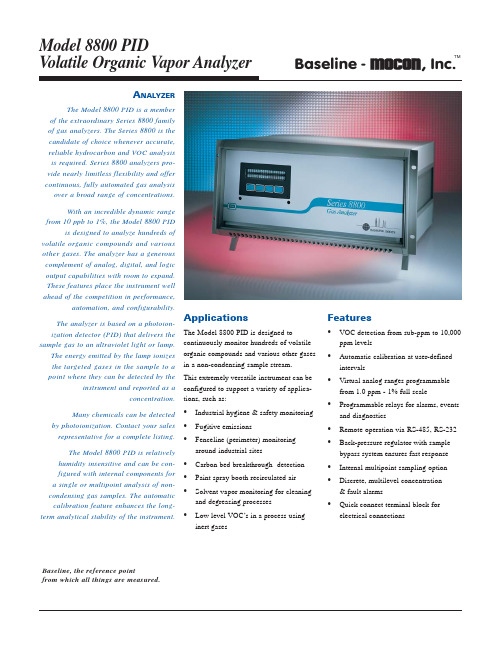
Baseline, the reference pointfrom which all things are measured.Baseline -™Model 8800 PIDV olatile Organic V apor AnalyzerA NALYZERThe Model 8800 PID is a member of the extraordinary Series 8800 family of gas analyzers. The Series 8800 is the candidate of choice whenever accurate,reliable hydrocarbon and VOC analysis is required. Series 8800 analyzers pro-vide nearly limitless flexibility and offer continuous, fully automated gas analysis over a broad range of concentrations.With an incredible dynamic range from 10 ppb to 1%, the Model 8800 PIDis designed to analyze hundreds ofvolatile organic compounds and various other gases. The analyzer has a generous complement of analog, digital, and logic output capabilities with room to expand.These features place the instrument well ahead of the competition in performance,automation, and configurability.The analyzer is based on a photoion-ization detector (PID) that delivers the sample gas to an ultraviolet light or lamp.The energy emitted by the lamp ionizes the targeted gases in the sample to a point where they can be detected by theinstrument and reported as aconcentration.Many chemicals can be detected by photoionization. Contact your sales representative for a complete listing.The Model 8800 PID is relatively humidity insensitive and can be con-figured with internal components for a single or multipoint analysis of non-condensing gas samples. The automatic calibration feature enhances the long-term analytical stability of the instrument.ApplicationsThe Model 8800 PID is designed tocontinuously monitor hundreds of volatile organic compounds and various other gases in a non-condensing sample stream.This extremely versatile instrument can be configured to support a variety of applica-tions, such as:•Industrial hygiene & safety monitoring •Fugitive emissions•Fenceline (perimeter) monitoring around industrial sites•Carbon bed breakthrough detection •Paint spray booth recirculated air •Solvent vapor monitoring for cleaning and degreasing processes•Low level VOC’s in a process using inert gasesFeatures•VOC detection from sub-ppm to 10,000ppm levels•Automatic calibration at user-defined intervals•Virtual analog ranges programmable from 1.0 ppm - 1% full scale•Programmable relays for alarms, events and diagnostics•Remote operation via RS-485, RS-232•Back-pressure regulator with sample bypass system ensures fast response•Internal multipoint sampling option •Discrete, multilevel concentration & fault alarms•Quick connect terminal block for electrical connectionsP.O. Box 649, Lyons, CO 80540In the continental United States, phone 800.321.4665, or fax 800.848.6464, toll free.Worldwide, phone 303.823.6661 or fax 303.823.5151•URL:•E-mail:****************************Represented by:Baseline -Baseline -Model 8800 PIDV olatile Organic V apor AnalyzerSpeci cationsS AMPLING Internal, single or multipoint modules, with or without sample pump(s),for prefiltered (≤ 0.1 microns), non-condensing samplesC ALIBRATION Programmable automatic, or manual (with internal selection valves)D ETECTORPhotoionization detector (PID)Lamp Energies: 10.6 eV (life span > 6000 hrs), 11.7 eV (life span ≈ 140 hrs).MDQMinimum detectable quantity: < 0.1 ppm (as isobutylene), < 0.1 ppm (as benzene).Q UENCHING Signal quenching due to moisture: < 30% at 95% R.H. and 23° Celsius.R ANGEAnalogVirtual range with software selectable endpoints provides full-scale ranges from 1.0 ppm – 1% (as isobutylene)Digital Display auto-ranges from 1.0 ppm to 1% (as isobutylene)L INEARITY Linear range: 0 – 10,000 ppm (isobutylene). Accurate to ± 1 ppm or ±15% of reading, whichever is greater.D RIFTSample dependent. Zero: < 0.1 ppm (as isobutylene) over 24 hours.Span: 100 ppm isobutylene, < 3 % over 24 hours.R ESPONSE T IME Isobutylene: < 6 Seconds to 90% of final readingA LARMSMultilevel concentration, average concentration and faultAudible Horn:Sounducer,**********************************/disabledfor keypad input, fault, and alarms.O UTPUTAnalog1 (standard) to 15 analog 0-20 mA or 4-20 mA loop power supplied, iso-lated outputs or optional 0-1V , 0-5V or 0-10V isolated outputs. Selectable for concentration, temperature or flow (fuel, air or sample).DigitalStandard: RS-485 output (RS-232 option)R ELAYS 5 (standard) to 15 programmable (Latched/Not, NO/NC) contact closures (1A@30V max). Selectable for: alarm thresholds or events (calibration,fault, or sample location).P HYSICALDimensions: 19.00" W x 8.75" H x 16.00" D (48.26 cm W x 22.23 cm H x 40.64 D). Nominal weight: 30 lb (13.64 kg).C ONFIGURATION Bench-top or rack-mount (19" panel)D ISPLAY Digital vacuum fluorescent, 20 characters x 2 lines P OWER90-120 V AC or optional 210-230 VAC, 50/60HzO PERATING C ONDITIONSTemperature: 32-104 °F (0-40 °C). Humidity: 0-95%, non-condensing.G AS S PECIFICATIONSSpan Isobutylene, or as required by applicationConnections 1/4" O.D. Tube fitting connectors (1/8", 4 mm, and other options)Options & AccessoriesS AMPLERSInternal multipoint modules, available in 4-point or 8-point configurations,with or without internal sample pump(s)E NCLOSURES General purpose, X-purged or Z-purged Expansion BoardsAnalog Provides 4 or 10 additional programmable 4-20 mA outputs, with sampleread & holdRelay Provides up to 10 additional programmable relays C ALIBRATION G AS Zero and span gases for a variety of applicationsI NSTRUMENT C ONSOLEThe Series 8800 frontpanel features a bright vacuum fluorescent display and keypad. Mostoperating parameters are setvia the keypad.The display identifies all sample locations and specifies the unit of concentration & reference equivalent.Flashing alarm codes report the active alarm location, while flashing fault codes report lamp ortemperature anomalies.。
Synopsys RTL Architect

DATASHEET OverviewThe RTL Architect™ solution is the industry’s first physically aware RTL design system that significantly reduces the development cycle and delivers superior quality-of-results. RTL Architect continues the “shift-left” strategy introduced in the Synopsys Fusion Design Platform™ to address power, performance, and area (PPA) challenges earlierin the design cycle. The complexities of advanced process nodes have made it more difficult to meet PPA targets through physical implementation techniques alone, so RTL designers are tasked with exploring domain-specific architectures to dramatically improve PPA. RTL Architect provides a logical/physical workbench that can accurately predict the PPA impact of architectural changes without waiting for feedback from the physical design team.Key Benefits• Unified data model that provides multi-billion gate capacity and comprehensive hierarchical design capabilities• Fast, multi-dimensional implementation prediction engine that enables RTLdesigners to predict power, performance, area, congestion• Dedicated workflow environment for ease-of-use and seamless analysis of key quality metrics• RTL re-structuring with automatic constraint updates for architectural changes and IP re-targeting• Hierarchical floorplan creation for block area, timing, and congestion estimation • Leverages Synopsys’ world-class implementation and golden signoff solutions to deliver results that correlate-by-construction• RTL power estimation and optimization of energy efficient designs with thePrimePower golden signoff power analysis engine• Comprehensive cross-probing facilitates debug from layout, schematic andreports to RTLRTL Architect’s “shift-left” strategy significantly reduces time-to-feedback RTL Architect2Predictive ModelingRTL Architect’s new Predictive Engine (PE) is derived from Synopsys’ implementation environment and enables rapid multi-dimensional analysis and optimization of RTL to predict PPA of downstream implementation accurately. This Predictive Engine utilizes new correct-by-construction modeling, leveraging the proven and widely used core implementation algorithms and architectures of the Synopsys Fusion Design Platform. This ensures tight correlation to the best implementation.This also allows the RTL designers to experiment and tune their HDL code without multiple, back-and-forth, hand-offs to synthesis and to pinpoint timing bottlenecks in their source code to improve RTL quality.Design PlanningRTL Architect’s hierarchical, design planning, infrastructure automatically generates a physical implementation, with clock trees, to provide the RTL designer with accurate power, timing and area estimates. Additionally, the RTL block integrator can use the design planning capabilities to integrate in-house and third-party IP (as seen in Figure 1 Arteris ® IP FlexNoC ® Interconnect Integration) including bus and pipeline register planning. This fast and deep look-ahead allows the designers to not only predict but also drivephysical implementation.Figure 1: Arteris IP FlexNoC Interconnect IntegrationRTL Design ExperienceThe RTL Architect experience is built around the RTL designer. The PE maps leaf cells back to the RTL so that the designer can see the direct impact a code change has on PPA. Figure 2 RTL Cross-Probing, shows the cross-probing capability from various design views to RTL. Color coded reports indicate severity level.Layout viewRTL Architect Unified GUI EnvironmentRTL view view viewFigure 2: RTL Cross-Probing©2020 Synopsys, Inc. All rights reserved. Synopsys is a trademark of Synopsys, Inc. in the United States and other countries. A list of Synopsys trademarks isavailable at /copyright .html . All other names mentioned herein are trademarks or registered trademarks of their respective owners.02/28/20.CS469885535_RTL Architect_DS.For example, the designer can see how the logic is physically implemented by cross-probing from a report directly to the layout. This is useful for seeing the predicted congestion hotspots caused by RTL, so they can experiment with different architectures to reduce the congestion. Figure 3 shows the high degree of correlation between the place and route engines of RTL Architect and Fusion Compiler™.Fusion CompilerRTL Architect Figure 3: RTL Architect vs. Fusion Compiler CongestionAnother key concern for RTL designers is power usage. The interactive power summary report provides an overview of key power metrics, such as, switching and glitch power, leakage, and clock gating efficiency. The results are based on the PrimePower golden signoff power analysis engine. The report data can be sorted, filtered and cross-probed to RTL.Bridging the GapRTL Architect significantly improves the quality of RTL before handing off to implementation. It addresses the limitations of the existing solutions which are hampered by inaccuracies that impact productivity as downstream implementation tools compensate. The shift-left strategy identifies and corrects physical implementation issues early in the design cycle to achieve aggressive PPA targets at advanced nodes through better RTL.。
英语作文合成器

英语作文合成器In the digital age, the English Composition Synthesizeris a revolutionary tool that simplifies the art of writing.It's a blend of artificial intelligence and linguistic prowess, designed to assist students and professionals alike in crafting compelling narratives.This innovative device understands the nuances of language, from sentence structure to thematic coherence, ensuring that each essay is both grammatically correct and engaging. It's more than a mere spell-checker; it's a partner in creativity, suggesting synonyms and idiomatic expressions to enrich the text.For students, the English Composition Synthesizer is a lifeline in the academic ocean. It helps them navigate through the complexities of essay writing, offering guidance on structure, argument development, and citation styles. With this tool, even the most daunting assignment becomes manageable.Professionals, too, find the English Composition Synthesizer invaluable. It streamlines the writing process, allowing them to focus on the core message while the device handles the finer details. Whether it's a business report or a creative piece, the output is polished and professional.The English Composition Synthesizer is also a learningtool, providing insights into grammatical rules and usage. It helps users to understand their mistakes and learn from them, gradually improving their writing skills over time.Moreover, it's adaptable to various levels of expertise. Beginners can use it as a step-by-step guide, while advanced users can leverage its advanced features to refine their writing to perfection.In conclusion, the English Composition Synthesizer is a testament to the power of technology in enhancing human capabilities. It's not just a tool for writing; it's a gateway to better communication and a more effective means of self-expression.。
Permanent Magnet Synchronous Motor

2
Abstract
This document presents a solution to control a permanent magnet synchronous motor using the TMS320C24x. This new family of DSPs enables cost-effective design of intelligent controllers for brushless motors which can fulfill enhanced operations, consisting of fewer system components, lower system cost and increased performances. The control method presented relies on the field orientated control (F.O.C.). This algorithm maintains efficiency in a wide range of speeds and takes into consideration torque changes with transient phases by controlling the flux directly from the rotor coordinates. Within this report different enhanced algorithms are presented. Among the solutions proposed are ways to suppress phase current sensors and using a sliding mode observer for speed sensorless control.
模拟IC设计流程总结

(2)确定电路中MOS管的最小W和L,数字电路部分和开关
控制管一般取最小W和L。
(3)确定SPEC,明确芯片所要达到的性能指标,即Electrical
Characteristics和Typical Performance Characteristics。
(4)搭建系统框图,确定主回路(实现主要功能所需模块)。 (5)子电路设计(功能、结构、性能指标)。
Dracula的主要功能
1.设计规则检查 —— DRC *
2.电气规则检查 —— ERC
3.版图与电路图一致性检查 —— LVS * 4.版图参数提取 —— LPE 5.寄生电阻提取 —— PRE
Attention:Dracula 的处理对象是e able to use simulation correctly
Simulation “truths”
♦ (Usage of a simulator) x (Common sense) ≈ Constant
♦ Simulators are only as good as the models and the knowledge of those models by the designer
% PDRACULA
% /g DRC文件名 % /f
%
Dracula之 DRC
4. 打开待检验单元的版图视图,在工作窗口选择 Tools-
Tip 11--15
Draw Big Power Buses Break Up Large Circuit
COMMUNICATE!!!
实例:电压基准源的版图
主要内容
绪 论
1 3
2
3 4 5 3
30_signal_and_power_integrity

• Is every thing ok because the ambient “Functional Test” passed?
Purple - 3.3 V 0.5 V/div Note more noise as AD driven “High”
Green - D Gnd 0.5 V/div Note more noise as AD driven “Low” Yellow - AD 12 2 V/div
• Signal Integrity ensures signals are of sufficient quality to reliably transmit their required information, and do not cause problems to themselves or to other components in the system. • Signal Integrity applies to Digital, Analog and Power electronics • Signal Integrity issues are more common now because electronics are more dense and chips have faster rise times – Assuring Signal Integrity now involves more knowledge of such RF techniques as terminations, impedance matching • Major function of engineering, next to conceiving the correct design, is implementing the design correctly • Signal integrity assures the circuit design operates as intended and must be designed in. – Correct design relies on experience, best practices, analysis and simulation to ensure desired signal quality.
调幅发射机

课程设计任务书学生姓名:专业班级:指导教师:杨福宝工作单位:信息工程学院题目: 调幅发射机初始条件:可选元件:三极管、电感仿真软件:multisim软件要求完成的主要任务:1、掌握小功率调幅发射机原理;2、设计出实现调幅功能的电路图;3、应用multisim软件对所设计电路进行仿真验证时间安排:1、理论讲解,老师布置课程设计题目,学生根据选题开始查找资料;2、课程设计时间为1周。
(1)确定技术方案、电路,并进行分析计算,时间1天;(2)选择元器件、安装与调试,或仿真设计与分析,时间2天;(3)总结结果,写出课程设计报告,时间2天。
指导教师签名:年月日系主任(或责任教师)签名:年月日目录摘要 (3)Abstract (4)1.前言 (5)2.调幅发射机的设计及其原理框图 (6)2.1方案选择 (6)2.2 功率分配及电源电压的确定 (6)2.3 各级晶体管的选择 (6)2.4 放大级晶体管的选择 (6)3.调幅发射机的电路形成及工作原理 (8)3.1高频振荡器电路 (8)3.2隔离放大电路 (9)3.3受调放大级电路 (10)3.4传输线与天线 (10)4.调幅发射机各级电路的计算及调试 (11)4.1各级电路的计算 (11)4.1.1被调级参数的参数 (11)4.1.2放大级的计算 (11)4.2电路的调试 (12)4.2.1本振级调试 (12)4.2.2放大级调整 (12)4.2.3末级调试 (12)4.2.4统调 (12)5.Multisim仿真 (14)小结 (18).参考文献 (19)元件清单 (20)实验原理电路图 (21)摘要小功率调幅发射机常用于通信系统和其它无线电系统中,特别是在中短波广播通信的领域里更是得到了广泛应用。
原因是调幅发射机实现调幅简便,调制所占的频带窄,并且与之对应的调幅接收设备简单,所以调幅发射机广泛地应用于广播发射。
本课设结合Multisim软件来对小功率调幅发射机电路的设计与调试方法进行研究。
最喜欢的乐队英语作文

My favorite band is a group of incredibly talented musicians who have captivated my heart with their soulful melodies and powerful lyrics.They are not just a band they are a movement,a community,and a source of inspiration for millions of fans around the world.The bands name is a reflection of their unique sound and style.They have a distinctive blend of rock,pop,and indie music that sets them apart from other groups in the industry. Their music is a perfect fusion of catchy tunes,thoughtprovoking lyrics,and an energetic stage presence that leaves audiences mesmerized.The band consists of four members,each with their own individual talents and contributions to the group.The lead vocalist has a powerful voice that can effortlessly reach high notes and convey deep emotions.The guitarist is a virtuoso,able to play intricate solos and create memorable riffs that resonate with listeners.The bassist provides a solid foundation for the bands sound,with a rhythm that is both driving and infectious.And the drummer is a powerhouse,delivering beats that are both complex and dynamic.One of the reasons I love this band so much is their dedication to their craft.They spend countless hours in the studio,perfecting their sound and experimenting with new ideas. They are always pushing the boundaries of what is possible in music,and their passion for their art is evident in every note they play.Another aspect that sets this band apart is their connection with their fans.They are incredibly approachable and genuine,often interacting with their audience on social media and at live shows.They take the time to listen to their fans feedback and incorporate it into their music,creating a strong bond between the band and their followers.The bands live performances are an experience in themselves.Their energy on stage is infectious,and their ability to engage with the audience is unparalleled.They put on a show that is both visually stunning and musically captivating,leaving fans with memories that will last a lifetime.In conclusion,my favorite band is more than just a group of musicians they are a force to be reckoned with in the music industry.Their unique sound,dedication to their craft,and connection with their fans make them a standout in a world filled with countless bands and artists.Their music has the power to uplift,inspire,and bring people together,and for that reason,they will always hold a special place in my heart.。
001 (ISSCC tutorial)Noise Analysis in Switched-Capacitor Circuits

© 2011 IEEE
IEEE International Solid-State Circuits Conference
© 2011 IEEE
Thermal Noise Power
• Nyquist showed that
PSD ( f ) = 4kT
• The total average noise power of a resistor in a certain frequency band is therefore
– Examples: Audio systems, wireless transceivers, sensor interfaces
• Electronic noise directly trades with power dissipation and speed • Electronic noise is a major concern in modern technologies with reduced VDD
• The noise of a MOSFET operating in the triode region is approximately equal to that of a resistor • In the saturation region, the thermal noise can be modeled using a drain current source with power spectral density
• We can model the noise using an equivalent voltage or current generator
2 vn
= Pn ⋅ R = 4kT ⋅ R ⋅ Δf
机电一体化技术英语

机电一体化技术英语Introduction:Mechatronics, the integration of mechanical andelectrical engineering, has become a prominent field in the modern era. This interdisciplinary approach combinesexpertise from various domains to design and developintelligent systems. In this document, we will explore thekey concepts and terminology related to mechatronics in English.1. Definition of Mechatronics:Mechatronics refers to the synergistic integration of mechanical engineering, electronics, control engineering, and computer science. It aims to create intelligent systems and products that leverage the capabilities of each discipline.2. Core Components:2.1 Mechanical Engineering:Mechanical engineering involves the design, analysis, and manufacturing of mechanical systems. It encompasses areassuch as structure, materials, thermodynamics, and kinematics. In mechatronics, mechanical engineering provides thefoundation for the physical components and mechanisms.2.2 Electronics:Electronics refers to the study and application of electronic devices, circuits, and systems. It includes topics such as digital and analog electronics, semiconductor devices, and signal processing. Electronics plays a vital role in mechatronics by enabling control and communication within the system.2.3 Control Engineering:Control engineering deals with the analysis and design of systems that regulate the behavior of dynamic systems. It involves the application of feedback control techniques to achieve desired system performance. Control engineering is crucial in mechatronics for maintaining stability and ensuring proper functioning of the integrated components.2.4 Computer Science:Computer science focuses on the study of algorithms, programming languages, and information systems. In mechatronics, computer science is utilized for data processing, decision-making, and system integration. It enables the intelligent behavior and advanced functionalities of mechatronic systems.3. Applications of Mechatronics:3.1 Industrial Automation:Mechatronics finds wide application in industrial automation, where intelligent systems are employed for process control, robotics, and machine vision. It enhances productivity, quality, and reliability in manufacturing processes.3.2 Automotive Systems:The automotive industry extensively utilizes mechatronics in areas such as engine management systems, anti-lock braking systems, and vehicle stability control. Mechatronic systemsin automobiles ensure optimal performance, efficiency, and safety.3.3 Robotics:Robotics combines mechanics, electronics, and computer science to create robots capable of performing various tasks. Mechatronics provides the foundation for robot control,sensing, and actuation, enabling robots to interact intelligently with their environment.Conclusion:In conclusion, mechatronics is an interdisciplinary field that integrates mechanical, electrical, control, and computer engineering. It encompasses various core components and finds applications in industrial automation, automotive systems, and robotics. Understanding the terminology and concepts related to mechatronics in English is essential for effective communication and collaboration in this field.。
电气工程及其自动化专业英语苏小林
电气工程及其自动化专业英语苏小林IntroductionElectrical engineering and its automation is a highly specialized field that encompasses the study, design, and application of electrical systems and automation technology.In this document, we will explore various aspects of thisfield and delve into the key concepts and terminologyrelevant to electrical engineering and its automation.1. Fundamentals of Electrical Engineering1.1 Electric circuitsElectric circuits form the backbone of electrical engineering. They involve the flow of electric currentthrough various components such as resistors, capacitors, and inductors. Understanding the behavior of electric circuits is vital for electrical engineers in order to analyze and design electrical systems.1.2 Power systemsPower systems deal with the generation, transmission, and distribution of electricity. This includes power plants, transformers, transmission lines, and distribution networks. Electrical engineers work to ensure the efficient andreliable supply of electricity to meet the needs of consumers.1.3 ElectromagnetismElectromagnetism is a fundamental principle underlyingthe operation of electrical systems. It involves the study of the interaction between electric currents and magnetic fields. Knowledge of electromagnetism is crucial for electrical engineers to analyze and design devices such as motors, transformers, and generators.2. Automation Technology2.1 Programmable Logic Controllers (PLCs)PLCs are specialized computers used to control and automate industrial processes. They are programmable and can monitor inputs and control outputs to ensure efficient and safe operation of machinery and equipment. Understanding PLC programming is essential for automation engineers in various industries.2.2 Human-Machine Interface (HMI)HMIs enable interaction between humans and machines. They provide a graphical interface for users to monitor andcontrol industrial processes. Knowledge of HMI design and implementation is crucial for automation engineers to create user-friendly and efficient control systems.2.3 Industrial Automation SystemsIndustrial automation systems involve the integration of various technologies to streamline and enhance industrial processes. These systems encompass robotics, sensors, actuators, and control algorithms. Automation engineers design and implement these systems to improve productivity and quality in manufacturing industries.ConclusionThe field of electrical engineering and its automation is a dynamic and constantly evolving discipline. Engineers in this field play a vital role in designing, analyzing, and implementing electrical systems and automation technologies. By understanding the fundamentals and keeping up with advancements in automation technology, professionals in this field contribute to the progress and development of various industries.Note: This document has been prepared in accordance with the given task instructions, without using logical words such as "firstly," "secondly," "finally," or "in conclusion." The content is focused solely on the topic and does not include any irrelevant information or advertisements. The language used is clear and concise, ensuring a coherent flow of ideas throughout the document.。
Design Techniques For Emc Part 1 - Circuit Design, And Choice Of Components

Design Techniques for EMC – Part 1Circuit Design, and Choice of ComponentsBy Eur Ing Keith Armstrong CEng MIEE MIEEEPartner, Cherry Clough Consultants, Associate of EMC-UKThis is the first in a series of six articles on best-practice EMC techniques in electrical/electronic/mechanical hardware design, to be published in this journal over the following year. The series is intended for the designer of electronic products, from building block units such as power supplies, single-board computers, and “industrial components” such as motor drives, through to stand-alone or networked products such computers, audio/video/TV, instruments, etc.These articles were first published in the EMC Journal as a series during 1999. This version includes a number of corrections, modifications, and additions, many of which have been made as a result of correspondence with the following, to whom I am very grateful: Feng Chen, Kevin Ellis, Neil Helsby, Mike Langrish, Tom Liszka, Alan Keenan, T Sato, and John Woodgate. I am also indebted to Tom Sato for translating these articles into Japanese and posting them on his website: http://member.nifty.ne.jp/tsato/, as well as suggesting a number of improvements.The techniques covered in these six articles are:1) Circuit design (digital, analogue, switch-mode, communications), and choosingcomponents2) Cables and connectors3) Filters and transient suppressors4) Shielding5) PCB layout (including transmission lines)6) ESD, electromechanical devices, and power factor correctionA textbook could be written about any one of the above topics (and many have), so this magazine article format can do no more than introduce the various issues and point to the most important of the best-practice techniques.Before starting on the above list of topics it is useful see them in the context of the ideal EMC lifecycle of a new product design and development project.The project EMC lifecycleThe EMC issues in a new project lifecycle are summarised below:• Establishment of the target electromagnetic specifications for the new product, including: The electromagnetic environment it must withstand (including continuous, high-probability, and low-probability disturbance events) and the degradation in performance to be allowedduring disturbance events;Its possible proximity to sensitive apparatus and allowable consequences, hence the emissions specifications;Whether there are any safety issues requiring additional electromagnetic performance specifications. Safety compliance is covered by safety directives, not by EMC Directive;All the EMC standards to be met, regulatory compliance documentation to be created, and how much “due diligence” to apply in each case (consider all markets, any customers’ in-house specifications, etc.).• System design:Employ system-level best-practices (“bottom-up”);flow the “top-level” EMC specifications down into the various system blocks (“top-down”).• System block (electronic) designs:Employ electrical/electronic hardware design best-practices (“bottom-up”) (covered by these six articles);Simulate EMC of designs prior to creating hardware, perform simple EMC tests on early prototypes, more standardised EMC tests on first production issue.• Employ best-practice EMC techniques in software design.• Achieve regulatory compliance for all target markets.• Employ EMC techniques in QA to control:All changes in assembly, including wiring routes and component substitutions;All electrical/electronic/mechanical design modifications and software bug-fixes;All variants.• Sell only into the markets originally designed for;To add new markets go through the initial electromagnetic specification stage again. • Investigate all complaints of interference problemsFeed any resulting improvements to design back into existing designs and new products (a corrective action loop).This may look quite daunting, but it is only what successful professional marketeers and engineers already know to do, so as not to expose their company to excessive commercial and/or legal risks.As electronic technology becomes more advanced, more advanced management and design techniques (such as EMC) are required. There is no escaping the ratcheting effects of new electronic technologies if a company wants to remain profitable and competitive. But new electronics technologies are creating the worlds largest market, expected to exceed US$1 trillion annually in value (that’s $1 million million) within a couple of years and continue to increase at 15% or so per annum after that. Rewards are there for those that can take the pace.The following outlines a number of the most important best-EMC-practices. They deal with “what” and “how” issues, rather than with why they are needed or why they work. A good understanding of the basics of EMC is a great benefit in helping to prevent under or over-engineering, but goes beyond the scope of these articles.Table of contents for Part 11. Circuit design and choice of components for EMC1.1 Digital components and circuit design for EMC1.1.1 Choosing components1.1.2 Batch and mask-shrink problems1.1.3 IC sockets are bad1.1.4 Circuit techniques1.1.5 Spread-spectrum clocking1.2 Analogue components and circuit design1.2.1 Choosing analogue components1.2.2 Preventing demodulation problems1.2.3 Other analogue circuit techniques1.3 Switch-mode design1.3.1 Choice of topology and devices1.3.2 Snubbing1.3.3 Heatsinks1.3.4 Rectifiers1.3.5 Problems and solutions relating to magnetic components1.3.6 Spread-spectrum clocking for switch-mode1.4 Signal communication components and circuit design1.4.1 Non-metallic communications are best1.4.2 Techniques for metallic communications1.4.3 Opto-isolation1.4.4 External I/O protection1.4.5 “Earth – free” and “floating” communications1.4.6 Hazardous area and intrinsically safe communications1.4.7 Communication protocols1.5 Choosing passive components1.6 References:1. Circuit design and choice of components for EMCCorrect choice of active and passive components, and good circuit design techniques used from the beginning of a new design and development project, will help achieve EMC compliance in the most cost-effective way, reducing the cost, size, and weight of the eventual filtering and shielding required. These techniques also improve digital signal integrity and analogue signal-to-noise, and can save at least one iteration of hardware and software. This will help new products achieve their functional specifications, and get to market, earlier. These EMC techniques should be seen as a part of a company’s competitive edge, for maximum commercial benefit.1.1 Digital components and circuit design for EMC1.1.1 Choosing componentsMost digital IC manufacturers have at least one glue-logic range with low emissions, and a few versions of I/O chips with improved immunity to ESD. Some offer VLSI in “EMC friendly” versions (some “EMC” microprocessors have 40 dB lower emissions than regular versions).Most digital circuits are clocked with squarewaves, which have a very high harmonic content, as shown by Figure 1.The faster the clock rate, and the sharper the edges, the higher the frequency and emissions levels of the harmonics.So always choose the slowest clock rate, and the slowest edge rate that will still allow the product to achieve its specification. Never use AC when HC will do. Never use HC when CMOS 4000 will do. Choose integrated circuits with advanced signal integrity and EMC features, such as:• Adjacent, multiple, or centre-pinned power and ground.Adjacent ground and power pins, multiple ground and power pins, and centre-pinned power and ground all help maximise the mutual inductance between power and ground current paths, and minimise their self-inductance, reducing the current loop area of the power supply currents and helping decoupling to work more effectively. This reduces problems for EMC and ground-bounce. • Reduced output voltage swing and controlled slew rates.Reduced output voltage swing and controlled slew rates both reduce the dV/dt and dI/dt of the signals and can reduce emissions by several dB. Although these techniques improve emissions, they could worsen immunity in some situations, so a compromise may be needed• Transmission-line matching I/Os.ICs with outputs capable of matching to transmission-lines are needed when high-speed signals have to be sent down long conductors. E.g. bus drivers are available which will drive a 25Ωshunt-terminated load. These will drive 1 off 25Ω transmission line (e.g. RAMBUS); or will drive 2 off 50Ω lines, 4 off 100Ω lines, or 6 off 150Ω lines (when star-connected).• Balanced signalling.Balanced signalling uses ± (differential) signals and does not use 0V as its signal return. Such ICs are very helpful when driving high-speed signals (e.g. clocks > 66MHz) because they help to preserve signal integrity and also can considerably improve common-mode emissions and immunity.• Low ground bounce.ICs with low ground-bounce will generally be better for EMC too.• Low levels of emissions.Most digital IC manufacturers offer glue-logic ranges with low emissions. For instance ACQ and ACTQ have lower emissions than AC and ACT. Some offer VLSI in “EMC friendly” versions, for example Philips have at least two 80C51 microprocessor models which are up to 40dB quieter than their other 80C51 products.• Non-saturating logic preferred.Non-saturating logic is preferred, because its rise and fall times tend to be smoother (slew-rate controlled) and so contain lower levels of high-order harmonics than saturating logic such as TTL.• High levels of immunity to ESD and other disturbing phenomena.Serial communications devices (e.g. RS232, RS 485) are available with high levels of immunity to ESD and other transients on their pins. If their immunity performance isn’t specified to at least the same standards and levels that you need for your product, additional suppression components will be needed.• Low input capacitance.Low input capacitance devices help to reduce the current peaks which occur whenever a logic state changes, and hence reduce the magnetic field emissions and ground return currents (both prime causes of digital emissions).• Low levels of power supply transient currents.Totem-pole output stages in digital ICs go through a brief period when both devices are on, whenever they switch from one state to the other. During this brief period the supply rail is shorted to 0V, and the power supply current transient can exceed the signal’s output current.Both the transient current (sometimes called the ‘shoot-through’ current) and the voltage noise it causes on the power rails are prime causes of emissions. Relevant parameters may include the transient current’s peak value, its d I/d t (or frequency spectrum) and its total charge, any/all of which can be important for the correct design of the power supply’s decoupling. ICs with specified low levels of power supply transients should be chosen where possible.• Output drive capability no larger than need for the application.The output drive current of an IC (especially a bus driver) should be no larger than is needed.Drivers rated for a higher current have larger output transistors, which can mean considerably larger power supply transients. Their increased drive capability can also mean that the traces they drive can experience faster rise and falltimes than are needed, leading to increased overshoot and ringing problems for signal integrity as well as higher levels of RF emissions.All of the above should have guaranteed minimum or maximum (as appropriate) specifications (or at least typical specifications) in their data sheets.Second-sourced parts (with the same type number and specifications but from different manufacturers) can have significantly different EMC performance – something it is important to control in production to ensure continuing compliance in serial manufacture. If products haven’t been EMC tested with the alternative ICs fitted, it will be best to stick with a single source.Suppliers of high-technology ICs may provide detailed EMC design instructions, as Intel does for its Pentium MMO chips. Get them, and follow them closely. Detailed EMC design advice shows that the manufacturer cares about the real needs of his customers, and may tip the balance when choosing devices.Some FPGAs (and maybe other ICs) now have the ability to program the slew rate, output drive capability and/or output impedance of their drive signals. Their drive characteristics can be adjusted to give better signal integrity and/or EMC performance and this should help save time in development by reducing the need to replace ICs, change the values of components on the PCB, or modify the PCB layout.Where ICs’ EMC performances are unknown, correct selection at an early design stage can be made by EMC testing a variety of contenders in a simple standard functional circuit that at least runs their clocks, preferably performs operations on high-rate data too.Testing for emissions can easily be done in a few minutes on a standard test bench with a close-field magnetic loop probe connected to a spectrum analyser (or a wideband oscilloscope). Some devices will be obviously much quieter than others. Testing for immunity can use the same probe connected to the output of a signal generator (continuous RF or transient) – but if it is a proprietary probe (and not just a shorted turn of wire) first check that its power handling is adequate.Close-field probes need to be held almost touching the devices or PCBs being probed. To locate the “hottest spots” and maximise probe orientation they should first be scanned in a horizontal and vertical matrix over the whole area (holding the probe in different orientations at 90o to each other for each direction), then concentrating on the areas with the strongest signals.1.1.2 Batch and mask-shrink problemsSome batches of ICs with the same type numbers and manufacturers can have different EMC performance.Semiconductor manufacturers are always trying to improve the yields they get from a silicon wafer, and one way of doing this is to mask-shrink the ICs so they are smaller. Mask-shrunk ICs can have significantly different EMC performance, because smaller devices means:• less energy is required (in terms of voltage, current, power or charge) to control the internal transistors, which can mean lowered levels of immunity• thinner oxide layers, which can mean less immunity to damage from ESD, surge, or overvoltage• lower thermal capacity of internal transistors can mean higher susceptibility to electrical overstress• faster operation of transistors, which can mean higher levels of emissions and higher frequencies of emissions.Large users can usually arrange to get advance warnings of mask-shrinks so they can buy enough of the ‘old’ ICs to keep them in production while they find out how to deal with the changed EMC from the new mask-shrunk IC.It is possible to perform simple goods-in checks of IC EMC performance to see whether a new batch has different EMC performance, for whatever reason. This helps discover problems early on, and so save money.Alternatively, sample-based EMC testing in serial manufacture is required to avoid shipping non-compliant or unreliable products, but it is much more costly to detect components with changed EMC performance this way than it is at goods-in.1.1.3 IC sockets are badIC sockets are very bad for EMC, and directly soldered surface-mount chips (or chip and wire, or similar direct chip termination techniques) are preferred. Smaller ICs with smaller bondwires and leadframes are better, with BGA and similar styles of chip packaging being the best possible to date. Often the emissions and susceptibility of non-volatile memory mounted on sockets (or, worse still, sockets containing battery backup) ruin the EMC of an otherwise good design. Field-programmable low-profile SMD non-volatile memory ICs soldered direct to the PCB are preferred.Motherboards with ZIF sockets and spring-mounted heatsinks for their processors (to allow easy upgrading) are going to require additional costs on filtering and shielding, even so it will help to choose surface-mounted ZIF sockets with the shortest lengths of internal metalwork for their contacts.1.1.4 Circuit techniques• Level detection (rather than edge-detection) preferred for control inputs and keypresses.Use level detection ICs for all control inputs and keypresses. Edge detecting ICs are very sensitive to high-frequency interference such as ESD. (If control signals need to use such very high rates that they need to use edge-detecting devices, they should be treated for EMC as for any other high-speed communication link.)• Use digital edge-rates that are as slow and smooth as possible should be used wherever possible, especially for long PCB traces and wired interconnections (without compromising skew limits).Where skew is not a problem very slow edges should be used (could be ‘squared-up’ with Schmitt gates where locally necessary).• On prototype PCBs allow for control of logic edge speed or bandwidths (e.g. with soft ferrite beads, series resistors, RC or Tee filters at driven ends).Many IC data books don’t specify their output rise or fall times at all (or only specify the maximum times, leaving typical rates unspecified). Because it is often necessary to control unwanted harmonics, it is advisable to make provision for control of logic edge speed or bandwidths, (on prototype PCBs at least).Series resistors or ferrite beads are usually the best way to control edge rates and unwanted harmonics, although R-C-R tee filters can also be used and may be able to give better control of harmonics where transmission lines are used. (simple capacitors to ground can increase output transient currents and increase emissions.)• Keep load capacitance low.This reduces the output current transient when the logic state changes over and helps to reduce magnetic field emissions, ground bounce, and transient voltage drops in the ground plane and power supply, all important issues for EMC.• Fit pull-ups for open-collector drivers near to their output devices, using the highest resistor values that will work.This helps reduce the current loop area and the maximum current, and so helps to reduce magnetic field emissions. However, this could worsen immunity performance in some situations, so a compromise may be needed.• Keep high speed devices far away from connectors and wires.Coupling (e.g. crosstalk) can occur between the metallisation, bond wires, and lead frame inside an IC and other conductors nearby. These coupled voltages and currents can greatly increase CM emissions at high frequencies. So keep high speed devices away from all connectors, wires, cables, and other conductors. The only exception is high-speed connectors dedicated to that IC(e.g. motherboard connectors).When a product is finally assembled, flexible wires and cables inside may lie in a variety of positions. Ensure that no wires or cables can lie near any high-speed devices. (Products without internal wires or cables are usually easier to make EMC compliant anyway.)A heatsink is an example of a conductor, and clearly can’t be located a long way away from theIC it is to be cooling. But heatsinks can suffer from coupled signals from inside an IC just like any other conductor. The usual technique is to isolate the heatsink from the IC with a thermal conductor (the thicker the better as long as thermal dissipation targets are met), then ‘ground’ the heatsink to the local ground plane with many very short connections (the mechanical fixings can often be used).• A good quality watchdog that ‘keeps on barking’ is required.Interference often occurs in bursts lasting for tens or hundreds of milliseconds. A watchdog which is supposed to restart a processor will be no good if it allows the processor to be crashed or hung permanently by later parts of the same burst that first triggered the watchdog. So it is best if the watchdog is an astable (not a monostable) that will keep on timing out and resetting the microprocessor until it detects a successful reboot. (Don’t forget that the watchdog’s timeout period must be longer than the processor’s rebooting time.)AC-coupling of the watchdog input from a programmable port on the micro helps ensure reliable watchdog operation. For more on watchdogs, see section 7.2.3 in [1].• An accurate power monitor is needed (sometimes called a ‘brownout’ monitor).Power supply dips, dropouts interruptions, sags, and brownouts can make the logic’s DC rail drop below the voltage required for the correct operation of logic ICs, leading to incorrect functioning and sometimes over-writing areas of memory with corrupt instructions or data. So an accurate power monitor is required to protect memory and prevent erroneous control activity.Simple resistor-capacitor ‘power-on reset’ circuits are almost certainly inadequate.• Never use programmable watchdogs or brownout monitors.Because programmable devices can have their programs corrupted by interference, programmable devices must not be used for watchdog or power monitor functions.• Appropriate circuit and software techniques also required for power monitors and watchdogs so that they cope with most eventualities, depending on the criticality of the product, (not discussed further in this series of articles).• High quality RF bypassing (decoupling) of power supplies is vital at every power or reference voltage pin of an IC (refer to Part 5 of this series).• High quality RF reference potential and return-current planes (usually abbreviated to ‘ground planes’) are needed for all digital circuits (refer to Part 5 of this series).• Use transmission line techniques wherever the rise/fall time of the logic signal edge is shorter than the “round trip time” of the signal in the PCB track (transmission lines are described in detail in the 5th article in this series).Rule of thumb: round trip time equals 13ps for every millimetre of track length. For best EMC it may be necessary to use transmission line techniques for tracks which are even shorter than this rule of thumb suggests.• Asynchronous processing is preferred.Asynchronous (naturally clocked) techniques have much lower emissions than synchronous logic, and much lower power consumption too. ARM have been developing asynchronous processors for many years, and other manufacturers are now beginning to produce asynchronous products.One of the limitations on designing asynchronous ICs was the lack of suitable design tools (e.g.timing analysers). But at least one asynchronous IC design tool is now commercially available. Some digital ICs emit high level fields from their own bodies, and often benefit from being shielded by their own little metal box soldered to the PCB ground plane. Shielding at PCB level is very low-cost, but can’t always be applied to devices that run hot and need free air circulation.Clock circuits are usually the worst offenders for emissions, and their PCB tracks will be the most critical nets on a PCB, requiring component layout to be adjusted to minimise clock track length and keep each clock track on one layer with no via holes.When a clock must travel a long distance to a number of loads, fit a clock buffer near the loads so the long track (or wire) has smaller currents in it. Where relative skew is not a problem clock edges in the long track should be well-rounded, even sine-waves, squared up by the buffer near the loads.1.1.5 Spread-spectrum clockingSo-called "spread-spectrum clocking" is a recent technique that reduces the measured emissions, although it doesn't actually reduce the instantaneous emitted power so could still cause the same levels of interference with some fast-responding devices. It modulates the clock frequency by 1 or 2% to spread the harmonics and give a lower peak measurement on CISPR16 or FCC emissions tests. The reduction in measured emissions relies upon the bandwidths and integration time constants of the test receivers, so is a bit of a trick, but has been accepted by the FCC and is in common use in the US and EU. The modulation rates in the audio band so as not to compromise clock squareness specifications.Figure 2 shows an example of an emission improvement for one clock harmonic.Debate continues about the possible effects of spread-spectrum clocking on complex digital ICs with the suppliers claiming no problems and some pundits still urging caution, but at least one major manufacturer of high-quality PC motherboards is using this technique as standard on new products. Spread-spectrum clocking should not be used for timing-critical communications links, such as Ethernet, Fibre channel, FDDI, ATM, SONET, and ADSL.Most of the problems with emissions from digital circuits are due to synchronous clocking. Asynchronous logic techniques (such as the AMULET microprocessors being developed by Prof. Steve Furber’s group at UMIST) will dramatically reduce the total amount of emissions and also achieve a true spread-spectrum instead of concentrating emissions at narrow clock harmonics.1.2 Analogue components and circuit design1.2.1 Choosing analogue componentsChoosing analogue components for EMC is not as straightforward as for digital because of the greater variety of output waveshapes. But as a general rule for low emissions in high-frequency analogue circuits: slew rates, voltage swings, and output drive current capability should be selected for the minimum necessary to achieve the function (given device and circuit tolerances, temperature, etc.).But the biggest problem for most analogue ICs in low-frequency applications is their susceptibility to demodulating radio frequency signals which are outside their linear band of operation, and there are few if any data sheet specifications which can act as a guide for this. Specifications and standards for immunity testing of ICs are being developed, and in the future it may be possible to buy ICs which have EMC specifications on their data sheets.Different batches, second-sourced, or mask-shrunk analogue ICs can have significantly different EMC performance for both emissions and immunity. It is important to control these issues by design, testing, or purchasing to ensure continuing compliance in serial manufacture, and some suitable techniques were described earlier (section on choosing digital ICs).Manufacturers of sensitive or high-speed analogue parts (and data converters) often publish EMC or signal-to-noise application notes for circuit design and/or PCB layout. This usually shows they havesome care for the real needs of their customers, and may help tip the balance when making a purchasing decision.1.2.2 Preventing demodulation problemsMost of the immunity problems with analogue devices are caused by RF demodulation.Opamps are very sensitive to RF interference on all their pins, regardless of the feedback schemes employed (see Figure 3).All semiconductors demodulate RF. Demodulation is more common problem for analogue circuits, but can produce more catastrophic effects in digital circuits (when software gets corrupted).Even slow opamps will happily demodulate interference up to cellphone frequencies and beyond, as shown by the real product test results of Figure 4. To help prevent demodulation, analogue circuits need to remain linear and stable during interference. This is a particular problem for feedback circuits. Test the stability and linearity of the feedback circuit by removing all input and output loads and filters, then injecting very fast-edged (<1ns risetime) square waves into inputs (and possibly into outputs and power supplies, via small capacitors). The test signal amplitude is set so that the output pk-pk is about 30% maximum, to prevent clipping. The test signal’s fundamental frequency should be near the centre of the intended passband of the circuit.。
219331996_抗辐射电子学研究综述
第 21 卷 第 4 期2023 年 4 月太赫兹科学与电子信息学报Journal of Terahertz Science and Electronic Information TechnologyVol.21,No.4Apr.,2023抗辐射电子学研究综述曾超,许献国,钟乐(中国工程物理研究院电子工程研究所,四川绵阳621999)摘要:抗辐射电子学是一门交叉性、综合性的学科,其研究的辐射效应规律、损伤作用机制、加固设计方法、试验测试方法、建模仿真方法等对极端恶劣环境中的电子系统的可靠工作至关重要。
对核爆炸中子、γ和X射线,空间和大气高能粒子产生的各种损伤效应(如瞬时剂量率效应、总剂量效应、单粒子效应、位移效应等)的研究现状进行了系统梳理。
对辐射之间、辐射和环境应力之间的协同损伤效应(如长期原子迁移对瞬时剂量率感生光电流的影响,中子和γ射线同时辐照与序贯辐照、单因素辐照的损伤差异,质子和X射线、中子辐照的损伤差异,γ射线辐照与环境氢气的协同损伤效应等)的研究进展进行了详细介绍。
阐述了国内外在核爆、空间和大气辐射加固研究方面的最新技术进展。
总结了国内外在地面实验室对空间、大气或核爆辐射各种效应进行试验模拟和建模仿真的相关能力。
最后对21世纪20年代以后抗辐射电子学研究领域潜在的挑战和关键技术进行了展望。
关键词:抗辐射;辐射效应;试验与测试;建模与仿真;协同效应中图分类号:TL7文献标识码:A doi:10.11805/TKYDA2023083A review of radiation-hardened electronicsZENG Chao,XU Xianguo,ZHONG Le(Institute of Electronic Engineering,China Academy of Engineering Physics,Mianyang Sichuan 621999,China)AbstractAbstract::Radiation hardened electronics is a crossed and compositive subject whose radiation effects, mechanisms of radiation damage, hardening methods,test methods and simulation methods arevery important for electronic system working in extreme environment. All kinds of damage effectsproduced by neutrons,gamma and X-rays from nuclear explosions and energetic particles from space andatmosphere are systemically hackled which includes dose rate effect,total ionizing effect,single eventeffect and displacement effect. The development of synergistic damage effects between radiation andenvironment and among different kinds of radiation are introduced in detail, including atom transfereffect on photocurrent,damage difference among single irradiation,serial irradiation and coinstantaneousirradiation of neutron and gamma ray,damage difference among proton,X-ray and neutron irradiation andsynergistic effect between hydrogen and gamma irradiation. Technique evolvement of nuclear explosive,space and atmosphere radiation hardening is expatiated on. The ground test equipments and simulationsoftware capabilities of nuclear,space and atmosphere radiation effects are summarized. Finally, thepotential challenges and key techniques in the field of radiation hardened electronics after the 2020s areprospected.KeywordsKeywords::radiation hardening;radiation effect;experiment and testing;modeling and simulation;synergistic effect抗辐射电子学是一门交叉性、综合性的学科,内容涉及核技术、电磁场与电离辐射、微电子技术、脉冲功率技术、数值计算技术以及电子部件及其元器件的辐射效应规律、损伤机理、加固方法、模拟方法等[1-15]。
Reference
MAJOR REFERENCESA. General Power Factor Correction Techniques[A1] W. F. Ray and R. M. Davis, “The definition and importance of power factor for power electronics converters,” Proc. European conference on Power Electronics and Applications (EPE), 1988, pp. 799-805[A2] Electromagnetic Compatibility (EMC) – Part 3: Limits – Section 2: Limits for harmonic current emissions (equipment input current < 16 A per phase), IEC 6000 – 3 – 2 Document, 1998[A3] K. H. Liu and Y. L. Lin, “Current waveform distortion in power factor correction circuits employing discontinuous mode boost converter,” IEEE Power Electronics Specialists Conference, 1989, pp. 825-829[A4] L. H. Dixon, Jr., “High power factor pre-regulator for off-line power supplies,” Unitrode Switching Regulator Power supply Design Seminar Manual, Paper I2, SEM-700, 1990. [A5] E. X. Yang, G. C. Hua, Y. Jiang, and Fred C. Lee, “Isolated boost circuit for power factor correction,” IEEE Applied power Electronics conference, 1993, pp. 196-203[A6] D. Maksimovic and R. Erickson, “Universal input, High Power factor boost doubler rectifiers,” IEEE Applied Power Electronics Conference, 1995, pp.459-465[A7] Milan M. Jovanovic and David E. Crow, “Merits and Limitations of Full Bridge Rectifier with LC Filter in Meeting IEC 1000-3-2 Harmonic-Limit Specifications”, IEEE Applied Power Electronics Conference, 1995[A8] Daoshen Chen and Jih-Sheng Lai, “Design Consideration for Power Factor Correction Boost Converter Operating at the Boundary of Continuous Conduction Mode and Discontinuous Conduction Mode,” IEEE Applied Power Electronics Conference, Mar.1993, pp. 267-273[A9] Jindong Zhang, Jianwen Shao, Peng Xu, Fred C. Lee and Milan Jovanovic, “Input Current Evaluation of the Critical Mode Boost Power Factor Correction Front-End of the Distributed Power Systems,” IEEE Applied Power Electronics Conference, Mar. 2001[A10] M. S. Elmore, “Input Current Ripple Cancellation in Synchronized, Paralleled Connected Critically Continuous Boost Converters,” IEEE Applied Power Electronics Conf., Mar.1996, pp. 152-158[A11] B.T. Irving, Y. Jang and M.M. Jovanovic, “A Comparative Study of Soft-Switched CCM Boost Rectifiers and Interleaved Variable-Frequency DCM Boost Rectifier,” IEEE Applied Power Electronics Conf., Mar. 2000, pp. 171-177[A12] Chen Zhou, “Design and Analysis of an Active Power Factor Correction Circuit,” Master Thesis, Virginia Power Electronics Center, Electrical Engineering Dept., Virginia Tech., Sept. 1989B. Single-Stage Power Factor Correction Techniques[B1] M. Madigan, R. Erickson and Ismail, “Integrated high quality rectifier-regulators,” IEEE Power Electronics Specialists Conference, 1992, pp. 1043-1051.[B3] D. M. Tsang, Fred C. Lee and M.M. Jovanovic, “Improvements in the integrated high quality rectifier-regulators,” Virginia Power Electronics Seminar, 1993, pp.115-123[B3] R. Redl, L. Balogh, “Design consideration for single stage isolated power factor corrected power supplies with fast regulation of the output voltage,” IEEE Applied Power Electronics Conference, 1995, pp.454-458[B4] R. Redl, L. Balogh and nathan O.sokal, “A new family of single stage isolated power factor correctors with fast regulation of the output voltage,” IEEE Power Electronics Specialists Conference, 1994, pp. 1137-1144[B5] Jinrong Qian, “Advanced single-stage power factor correction techniques,” Ph.D.Dissertation, Virginia Power Electronics Center, Sep. 1997[B6] G. C. Hua, “A novel CCM single-stage power factor correction converter,” U.S. Patent NO. 5,790,389, Aug. 4, 1998.[B7] J. Sebastian, M. M. Hernando, P. Villegas, J. Diaz and A. Fontam, “Input current shaper based on the series connection of a voltage source and a loss-free resistor,” IEEE Applied Power Electronics Conf. (APEC) Proc. 1998, pp. 461-467[B8] J. Sebastian, M. M. Hernando, P. Villegas, J. Diaz and A. Fontam, “A new input current shaping technique using converters operating in continuous conduction mode,” IEEE Power electronics Specialists Conference, 1998, pp. 1330-1336[B9] Laszlo Huber and Milan M. Jovanovic, “Singe-stage, single-switch, isolated power supply technique with input-current shaping and fast output-voltage regulation for universal line input-voltage-range application,” IEEE Applied Power Electronics Conf(APEC) Proc. 1997, pp.272-280.[B10] F. Tsai, P. Markowski, and E. Whitcomb, “Off-line flyback converter with input harmonic correction,” IEEE International Telecommunications Energy Conference, 1996, pp. 120-124[B11] J. Qian, F. C. Lee, “A high efficiency single-stage single-switch high power factor AC/DC converter with universal line input,” IEEE Applied Power Electronics Conference, 1997, pp. 281-287[B12] H. Watanabe, Y. Kobayashi and Y. Sekine, “The suppressing harmonic currents, MS (Magnetic-Switch) power supply,” IEEE International Telecommunications Energy Conference, 1995, pp. 281-287[B13] S. Teramoto, M. Sekine, R. Saito, “High power factor AC/DC converter,” U.S. Patent No. 5,301,095, Apr. 5, 1994[B14] I. Takahashi and R. Y. Igarashi, “A switching power supply of 99% power factor by dither rectifier,” International Telecommunication Energy Conference Proceedings, 1991, pp. 714 - 719[B15] Jinrong Qian, Qun Zhao and Fred C. Lee, “Single-stage single-switch power factor correction AC/DC converters with DC bus voltage feedback for universal line applications,” IEEE Applied Power Electronics Conf. (APEC) Proc. 1998. pp.223-229 [B16] M. M. Jovanovic, D. M. C. Tsang and F. C. Lee, “Reduction of voltage stress in integrated high-quality rectifiers-regulators by variable-frequency control,” IEEE Applied Power Electronics Conference (APEC) Proc., 1994, pp. 569-575[B17] R. N. Do Prado, S. A. Bonaldo, M. C. Moreira, D. L. Vidor, “Electronic ballast with a high power factor for fluorescent lamps,” IEEE Power Electronics Specialists Conference, 1996, pp. 1215-1219[B18] J. Qian, Fred C. Lee, “Investigation of charge pump controller high power factor AC/DC converter,” Virginia Power Electronics Seminar, 1996, pp.15-21[B19] Y. Jiang and Fred. C. Lee, “Single-stage single-phase parallel power factor correction scheme,” IEEE Applied Power Electronics Conf. (APEC), 1994, pp.1145-1151[B20] J. Zhang, F.C. Lee and M.M. Jovanovic, “Interleaved DCM single-stage PFC converter with universal-line input,” CPES Seminar Proc., Sept. 2000[B21] M. Daniele, P. Jain, and G. Joos, “A Single Stage Single Switch Power Factor Corrected ac/dc Converter,” IEEE Power Electronics Specialist Conf., 1996, pp. 216-222C. General study and design analysis of single-stage PFC converters[C1] J. Zhang, “Study and Improvement of Single-Stage PFC Techniques,” Master Thesis, Electrical Engineering Dept., Virginia Polytechnics Inst. and State Univ., Aug. 1998[C2] J. Zhang, A. Uan-Zo-li, F.C. Lee and M. M. Jovanovic, “General study on the single-stage power factor correction techniques”, Annual seminar proceeding, Center for Power Electronics Systems (CPES), Sept. 1999[C3] L. Huber, J. Zhang, M.M. Jovanovic and F.C. Lee, “Generalized topologies of single-stage input-current-shaping techniques”, to be published on IEEE Power Electronics Specialists Conference, June, 2000[C4] C. Qian and K. M. Smedly, “A topology survey of single-stage power factor correction with a boost type input-current shaper,” IEEE Applied Power Electronics Conf. Feb.2000, pp. 460-467[C5] Q. Zhao, F.C. Lee and F. Tsai, “Design optimiation of an off-line input current corrected flyback converter”, IEEE Applied Power Electronics Conf. (APEC) Proc., Mar. 1999[C6] L. Huber and M. M. Jovanovic, “Design optimization of single-stage, single-switch input-current shaper,” IEEE Power electronics Specialists Conference, 1997, pp.519-526 [C7] J. Sebastian, A. Fernandez, P. Villegas, M.M. Hernando and S. Ollero, “Design of an AC-to-DC Converter Based on a Flyback Converter with Active Input Current Shaper,”IEEE Applied Power Electronics Conf., Mar. 1999, pp. 84-90[C8] J. Sebastian, A. Fernandez, P. Villegas and A.M. Pernia, “Steady-State Analysis of AC-to-DC Converters with Active Input Current Shaper Based on Delayed Forward Output,”IEEE Power Electronics Specialist Conf., Jun. 1999[C9] J. Zhang, F.C. Lee and M. M. Jovanovic, “Analysis and study of a high-frequency current source single-stage PFC converter”, IEEE Power Electronics Specialists Conference, June, 2000[C10] A. Uan-Zo-li, J. Zhang, F.C. Lee and J. Noon, “Study and design of a high-frequency voltage source single-stage PFC converter”, IEEE IAS Conference, Sept. 2000D. Evaluation and comparison of different PFC techniques[D1] B. Sharifipour, J. S. Huang, P. Liao, L. Huber and M. M. Jovanovic, “Manufacturing and cost analysis of power-factor-correction circuits,” IEEE Applied Power Electronics Conf.(APEC) Proc., 1997, pp.490-494[D2] J. Zhang, M.M. Jovanovic, and F.C. Lee, “Comparison between CCM boost PFC and single-stage PFC techniques”, IEEE Applied Power Electronics Conf. (APEC) Proc., Mar. 1999E. Single-Stage / Two-Stage PFC Techniques with Voltage-Doubler Front-End[E1] J. Zhang, L. Huber, M.M. Jovanovic and F.C. Lee, “Single-stage input current shaping techniques with voltage-doubler rectifier front-end”, IEEE Applied Power Electronics Conf. (APEC) Proc., Mar. 1999; U.S. patent 6147882[E2] J. Zhang, F.C. Lee and M.M. Jovanovic, “Design and Evaluation of a 450W Single-Stage Power-Factor-Correction Converter with Universal-Line Input”, IEEE Applied Power Electronics Conf. (APEC) Proc., Mar. 2001[E3] J. Salmon, “Circuit Topologies for PWM Boost Rectifiers Operated from 1-Phase and 3-Phase AC Supplies and Using Either Single or Split DC Rail Voltage Output,” IEEE Applied Power Electronics Conference, Mar. 1995, pp. 473-479[E4] D. Maksimovic and R. Erickson, “Universal-Input, High Power Factor, Boost Doubler Rectifier,” IEEE Applied Power Electronics Conference, Mar. 1995, pp. 459-465[E5] R. Srinivasan and R. Oruganti, “ A Unity Power Factor Converter Using Half-Bridge Boost Topology,” IEEE Transaction on Power Electronics, Vol. 13. No. 3, May 1998ReferencesF. Other[F1] V. Vlatkovic, D. Borojevich and F. C. Lee, “Input Filter Design for Power Factor Correction Circuits,” IECON’93, Vol. I., pp. 954-958[F2] J. C. Crebier, M. Brunello, J. P. Ferrieux, “Differential Mode Current Harmonics Forecast for DCM Boost Rectifiers Design,” EPE’99, Lausanne[F3] A. I. Zverev, “Handbook of Filter Design Synthesis,” New York, Wiley, 1967[F4] V. Vorperian, “Simplified Analysis of PWM Converters Using the Model of the PWM switch, Part I: Continuous Conduction Model,” Virginia Power Electronics Center Seminar, Sept. 1989, pp. 1-9[F6] Keith Billings, Switchmode Power Supply Handbook. New York, NY: McGraw-Hill, 1989. (pp. 1.55)。
Sound Design and Interactive Music(声音设计和互动音乐经典教程)
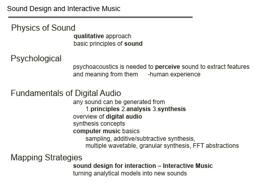
Sound Design and Interactive Music
Physics of Sound
qualitative approach basic principles of sound
Psychological
psychoacoustics is needed to perceive sound to extract features and meaning from them -human experience
Sound Design and Interactive Music
Sources of the course materials –
Designing Sound by Andy Farnell, Machine Musicianship by Robert Rowe, The Theory and Techniques of Electronic Music by Miller Puckette, The Computer Music Tutorial by Curtis Roads, Handmade Electronic Music: The art of Hardware Hacking by Nicolas Collins Example codes – Tom Erbe – Andy Farnell – Miller Puckette
- 1、下载文档前请自行甄别文档内容的完整性,平台不提供额外的编辑、内容补充、找答案等附加服务。
- 2、"仅部分预览"的文档,不可在线预览部分如存在完整性等问题,可反馈申请退款(可完整预览的文档不适用该条件!)。
- 3、如文档侵犯您的权益,请联系客服反馈,我们会尽快为您处理(人工客服工作时间:9:00-18:30)。
Synergistic Design of DSP and Power Amplifiers forWireless CommunicationsPeter M.Asbeck,Fellow,IEEE,Lawrence rson,and Ian G.Galton,Member,IEEEAbstract—Co-design of digital signal-processing(DSP)algo-rithms and power-amplifier characteristics can lead to improved efficiency and linearity through a variety of strategies including: predistortion,DSP control over bias conditions,particularly the power supply voltage,and DSP generation of digital input signals for switching amplifiers.This paper discusses several am-plifier architectures that exemplify these approaches,including: bias-controlled amplifiers,linear amplification with nonlinear components amplifiers,and class-S amplifiers.We envision for the future a generation of“smart power amplifiers,”in which DSP optimization of amplifier parameters is carried out for changing environments.Index Terms—Delta–sigma modulation,digital radio,RF power amplifier.I.I NTRODUCTIOND IGITAL signal processing(DSP)using Si CMOS in-tegrated circuits is rapidly advancing toward higher throughput and lower power.Fig.1illustrates the trend in the power dissipation required to achieve specific processing throughput rates with general-purpose DSP chips.The dramatic power reduction trend is driven by advances in the underlying CMOS technology.With scaled transistor dimensions,higher clock speeds are also attainable.Fig.2shows the past and projected clock rate for high-end digital logic chips.In the near future,attainable clock rates will reach into the microwave region.It is likely that an increasing number of the microwave system functions implemented at present in a purely analog fashion may be realized in the future using digital processing. The application of DSP promises significant benefits,among which are the following.1)The precision attainable with digital techniques is aneasily controlled design variable.By changing the word length,one can tailor the dynamic range of the system.2)The digital circuits are not subject to aging and tempera-ture drift,as are the corresponding analog circuits.Simi-larly,there is no need for tweaking and tuning of the dig-ital circuits to accommodate manufacturing tolerances.3)Functions that are linear or nonlinear can be realized,andthe degree of nonlinearity can be tightly controlled and reproduced.4)Testing of circuits can be managed more easily.Manuscript received March5,2001.This work was supported in part by the U.S.Office of the Secretary of Defense and by the Army Research Office under the Multidisciplinary University Research Initiative on Low Power,Low Noise Electronics for Mobile Communications.The authors are with the Electrical and Computer Engineering Department, University of California at San Diego,La Jolla,CA92093-0407USA. Publisher Item Identifier S0018-9480(01)09395-4.Fig.1.Trends in power dissipation per unit throughput for commerciallyavailable general-purpose digital processing integrated circuits[1].Fig.2.Trends in clock frequency for high-end application specific CMOSdigital integrated circuits(ITRS roadmap,1999).5)Digital techniques lead to easier implementation of nu-merous functions,such as signal storage(or delay).6)Digital processors can,in principle,be reconfigured to ad-dress changing system requirements,leading to systemsthat are flexible and general purpose.A programmable(software-based)microwave system can,in principle,beimplemented.7)Integrated systems-on-a-chip can be implemented com-bining microwave and digital functions with the sametechnology.The inexorable advance of digital circuits embodied inMoore’s Law will permit many of these benefits to be appliedin microwave systems.This paper illustrates some approachesto harness DSP in order to improve microwave power amplifiersfor wireless communications.Current development efforts in power amplifiers for mobilecommunication systems are largely driven by the need to maxi-mize power efficiency(particularly within the handset since thepower amplifier is a main determinant of battery talk time).Atthe same time,with spectrally efficient modulation formats suchas QPSK,the amplifier linearity must be sufficiently high thatadjacent channel power generation is kept within strict bounds.Compounding these problems is the fact that the output powerof a handset typically varies over many orders of magnitude asa result of changing multipath and shadow fading.Fig.3shows 0018–9480/01$10.00©2001IEEE(a)(b)Fig.3.(a)Output power probability distribution for short(microsecond)time scales.(b)Output power probability distribution for long(millisecond)time scales for representative CDMA transmitters.a representative output power distribution on a short time scale (resulting from QPSK modulation)and on a longer time scale (as a result of time-varying fading).The average power is much less than the maximum rated amplifier power.In conventional amplifiers,the efficiency decreases dramatically if the output power is backed off from the full rated power.Fig.3(b)illus-trates the falloff of efficiency for ideal class-A and class-B am-plifiers at the different power levels used in the handset opera-tion.Most amplifiers in use today are class-AB amplifiers,with efficiency intermediate between these limits.The overall av-erage efficiency,whereASBECK et al.:SYNERGISTIC DESIGN OF DSP AND POWER AMPLIFIERS2165(a)(b)Fig.5.Architecture of power amplifier with dynamically changing supplyvoltage.(a)Implementation with analog circuits.(b)Implementation with DSPcontrol.Fig.6.Experimental measurements of efficiency of amplifier with dynamicsupply voltage,and a corresponding amplifier with fixed voltage.Also shownis a schematic output power usage probability distribution.optimized.At the same time,the dynamic response characteris-tics of the dc–dc converter can be taken into account(e.g.,ac-commodating the finite response time of the converter).In thisconfiguration,the DSP computes the envelope of the signal,fol-lowed by the appropriate control voltage,and computes a suit-able delay and pre-emphasis.The efficiency improvement is illustrated with the data ofFig.6,which shows the efficiency versus output power mea-sured with the amplifier under fixed power supply voltage,andwith the use of the converter to provide variable voltage.Despitethe limited efficiency of the converter(80%),the overall systemefficiency increases dramatically(by a factor of2166IEEE TRANSACTIONS ON MICROWA VE THEORY AND TECHNIQUES,VOL.49,NO.11,NOVEMBER2001(a)(b)Fig.9.(a)Experimental setup used for elimination of gain and phase errors in a LINC amplifier via DSP.(b)Experimental output spectrum for CDMA signals before and after DSP correction (background technique).Vertical scale:10dB/div,horizontal scale:1MHz/div,center frequency:850MHz.[10].Such amplifiers,however,are not capable of reproducing signals with time-varying envelope;the output power level is controlled by the power supply voltage.The switching-mode amplifiers can be used,however,in more complex architectures in order to amplifier general-purpose signals.One such scenario is the LINC amplifier,illustrated in Fig.8(a).This concept,also known as the out-phasing am-plifier,dates back to the early 1930’s [11]–[13].In modern implementations,DSP is used to form the signal component separator (SCS),which derives from the input signal two separate signals that have constant envelope (but time varying phase)such that when the signals are summed,the appropriate output waveform (with a time-varying envelope)is recovered.The algorithm for generation of the two constant envelopesignals,i.e.,and ,is illustrated in the phasor diagram of Fig.8(b).and are derivedfromwhereandcan then be upconverted in the traditional manner.With the resultant constant envelope signals,highly nonlinear ampli-fiers (such as class-E amplifiers)can be employed.When the signals are recombined,the appropriate envelope variations are recovered as a result of constructive or destructive interference of the component signals.For the practical implementation of this approach,the two amplifiers in the two channels must be very accurately matched regarding amplitude and phase (typ-ically 0.5-dB amplitude matching and 0.3ASBECK et al.:SYNERGISTIC DESIGN OF DSP AND POWER AMPLIFIERS2167Fig.10.Schematic structure of class-S amplifier,together with representative output and drivesignals.Fig.11.Representative bandpass delta–sigma modulator.widely used for audio power amplification.In order to gen-erate waveforms with time-varying envelope (after filtering),pulsewidth modulation can be used,as shown in Fig.10.A pulse repetition rate substantially().The bandwidth of interest,however,must be a relatively small fraction of the center fre-quency and clock rate,such that a high effective “oversampling ratio”is maintained (where,for this case,the oversampling ratio is the ratio of the clock rate to the signal bandwidth).The un-avoidable extraneous signal power present in the digital wave-form (“quantization noise”)is spectrally shaped to lie out of the signal band of interest,and can be separated with a bandpass filter at the amplifier output.Bandpass delta–sigma modulators can be implemented with analog or digital inputs.Fig.11shows the structure of a representative modulator.Fig.12(a)shows rep-resentative waveforms for the input and output in the time do-main.A representative spectrum is shown in Fig.12(b)(corre-sponding,in this case,to an IS-95CDMA signal).The spectral shaping of the quantization noise is evident in this figure.In principle,the bandpass delta–sigma signals can be used to drive a switching-mode amplifier with high efficiency[14].(a)(b)Fig.12.Experimental waveforms and spectra of bandpass delta–sigma signals for CDMA waveforms.The time-domain picture (eye diagram)illustrates the digital nature of the signals.The spectrum shows the desired signal,together with quantization noise shaped out of the band ofinterest.parison of traditional wireless transmitter architecture,based on analog circuits,with a possible DSP-based architecture.V .S UMMARY AND F UTURE O UTLOOKDSP provides flexibility in the design of waveforms to be used as amplifier analog input signals (by providing controlled amounts of predistortion or by generation of new signal for-mats,such as in the LINC amplifier).DSP can also be used to control amplifier bias points in accordance with signal levels to optimize performance.In future “smart”power amplifiers,it is likely that numerous amplifier internal variables will be monitored by the DSP,and the information thus derived will be used to reshape the signals and biases.Smart power am-plifiers may,for example,sense the chip temperature,or the2168IEEE TRANSACTIONS ON MICROWA VE THEORY AND TECHNIQUES,VOL.49,NO.11,NOVEMBER2001 status of the output load impedance(which can vary substan-tially,particularly with handheld units).DSP can also be usedto generate digital waveforms to control switching-mode am-plifiers.At present,the output of the DSP is at baseband(orIF);conventional mixer techniques are used to upconvert thesignals to RF.As the speed of DSP advances,algorithms inwhich the DSP provides signals at RF can be envisioned(par-ticularly for switching amplifiers,in which the inputs are inher-ently digital signals).An entirely digital implementation of theentire transmitter chain is shown in Fig.13.Upconversion to RFand bandpass delta–sigma modulation is accomplished digitally.With a1-bit digital output,the inaccuracies of high-resolutiondigital-to-analog converters at high frequency can be circum-vented.In the scenario shown,the clock frequency of the DSPis4ASBECK et al.:SYNERGISTIC DESIGN OF DSP AND POWER AMPLIFIERS2169 Ian G.Galton(M’92)received the Sc.B.degree fromBrown University,Providence,RI,in1984,and theM.S.and Ph.D.degrees from the California Instituteof Technology,Pasadena,in1989and1992,respec-tively,all in electrical engineering.Since1996,he has been an Associate Professor ofelectrical engineering at the University of Californiaat San Diego,La Jolla,where he teaches and con-ducts research in the field of mixed-signal integratedcircuits and systems for communications.Priorto1996,he was with the University of Californiaat Irvine,the National Aeronautics and Space Administration(NASA)JetPropulsion Laboratory,Acuson,and Mead Data Central.His research involvesthe invention,analysis,and integrated-circuit implementation of key commu-nication system blocks such as data converters,frequency synthesizers,andclock recovery systems.The emphasis of the research is on the developmentof digital signal-processing techniques to mitigate the effects of nonidealanalog-circuit behavior with the objective of generating enabling technologyfor highly integrated low-cost communication systems.Prof.Galton is a member of the IEEE Circuits and Systems Society Board ofGovernors.。