20150728_bdti_adreno_white_paper_final
实测高通Adreno GPU控制面板 手机也可以像PC一样调游戏参数
实测高通Adreno GPU控制面板手机也可以像PC一样调游戏参数作者:来源:《电脑报》2020年第36期近日,小米10至尊纪念版已经适配Game Turbo 4.0,首次内置了Game Tuner功能,可定制游戏画面参数,提供标准、省电、均衡、高质量、自定义五个模式,可针对不同玩家、不同游戏的需求,给予最适合的图形参数设置。
而且,它还开放了抗锯齿、各向异性过滤、纹理过滤质量等详细的参数设置,熟悉PC游戏的玩家是不是突然就坐不住了?这些PC大作上才有的设置,对于那些深度游戏玩家来说,其实是一直在等待的功能。
虽然是小米10系列都将支持Game Turbo 4.0,但是目前仅有小米10至尊纪念版开放了该功能,我们本次体验的机型,自然也是这款机型。
而小米的其他机型,以及其他搭载了高通骁龙865平台的用户也别太心急,官方虽然没有明确表示,但是也透露了一个消息:作为上游供应商,高通也专门为这个新功能发微博站台。
显然,这个全新的功能,其实是高通骁龙865平台的特性,小米10系列,也只是“率先支持”,其他机型应该已经在进行适配,正式上线的日子应该不会太远。
其实回想高通骁龙865平台发布的时候,就已经提到过,骁龙865支持全新的Adreno可更新图形驱动技术,也就是说,用户可以像更新APP一样更新GPU驱动。
这也是此前在PC 平台上的特性,而用户可以升级驱动程序,让硬件随时保持最佳的性能,通过软件就能提升图形性能。
而此前的小米10 Pro也是最早支持该技术的机型之一,看得出来高通和小米在这方面的合作,不仅仅是简单的芯片供应商,还在技术上提供了非常多的支持,比如高端游戏的稳定性、Vulkan驱动性能提升等。
所以,建議使用高通骁龙865机型的用户,都看看自己的系统设置或者游戏空间,有没有相关的选项,将GPU驱动升级到最新版本,以体验最佳的游戏性能。
这次的Game Tuner,高通仍然选择小米的产品作为首发机型,可以看到,在“游戏加速”(也就是大家熟悉的游戏空间)功能中,新增了GPU设置(高级设置)的按钮,点击它就可以看到一个全新的控制台。
nvidia常用桌面显卡核心参数

GTX580GPU 引擎规格:CUDA处理器核心512显卡频率(MHz) 772 MHz核心频率(MHz) 1544 MHz纹理填充率(10亿/秒)) 49.4显存规格:显存频率(MHz) 2004标配显存配置1536 MB GDDR5显存位宽384-bit显存带宽(GB/秒) 192.4支持的特性:NVIDIA SLI®-ready¹ 三路NVIDIA 3D立体幻镜™NVIDIA PureVideo® 技术³ HD NVIDIA PhysX™-readyMicrosoft DirectX 11 OpenGL 4.0支持的总线PCI-E 2.0 x 16 Windows 7认证HDCPGPU 最高温度(摄氏) 97 C显卡最大功率(瓦) 244 W系统电源最低要求(瓦) 600 W辅助电源连接器一个6针,一个8针GTX570GPU 引擎规格:CUDA处理器核心480显卡频率(MHz) 732核心频率(MHz) 1464纹理填充率(10亿/秒)) 43.9显存规格:显存频率(MHz) 1900标配显存配置1280 MB GDDR5显存位宽320-bit显存带宽(GB/秒) 152.0支持的特性:NVIDIA SLI®-ready¹ 三路NVIDIA 3D立体幻镜™NVIDIA PureVideo® 技术³ HD NVIDIA PhysX™-readyMicrosoft DirectX 11 OpenGL 4.1支持的总线PCI-E 2.0 x 16 Windows 7认证HDCP标准显卡尺寸:高度 4.376英寸(111 mm) 长度10.5英寸(267 mm) 宽度双槽宽散热器以及电源规格:GPU 最高温度(摄氏) 97 C显卡最大功率(瓦) 219系统电源最低要求(瓦) 550辅助电源连接器两个6针连接器GTX480GPU 引擎规格:CUDA处理器核心480显卡频率(MHz) 700 MHz核心频率(MHz) 1401 MHz纹理填充率(10亿/秒) 42显存规格:显存频率(MHz) 1848标配显存配置1536 MB GDDR5显存位宽384-bit显存带宽(GB/秒) 177.4支持的特性:支持NVIDIA SLI®技术2-way/3-Way支持GeForce®(精视™)3D立体幻镜™NVIDIA 3D Vision Surround ReadyNVIDIA CUDA™ 技术Two Dual Link DVI 多显示器HDMIGTX470GPU 引擎规格:CUDA处理器核心448显卡频率(MHz) 607 MHz核心频率(MHz) 1215 MHz纹理填充率(10亿/秒) 34.0显存规格:显存频率(MHz) 1674标配显存配置1280 MB GDDR5 显存位宽320-bit显存带宽(GB/秒) 133.9支持的特性:支持NVIDIA SLI®技术2-way/3-Way支持GeForce®(精视™)3D立体幻镜™NVIDIA PureVideo® 技术HD支持NVIDIA PhysX™Microsoft DirectX 11OpenGL 4.1支持的总线PCI-E 2.0 x 16Windows Vista认证HDMIGTX460GPU 引擎规格:显卡版本GTX 460 1GB GDDR5 GTX 460 768MB GDDR5 GTX 460 SE CUDA处理器核心336 336 288显卡频率(MHz) 675 MHz 675 MHz 650 MHz 核心频率(MHz) 1350 MHz 1350 MHz 1300 MHz 纹理填充率(10亿/秒)) 37.8 37.8 31.2显存规格:显卡版本GTX 460 1GB GDDR5 GTX 460 768MB GDDR5 GTX 460 SE 显存频率(MHz) 1800 1800 1700标配显存配置 1 GB GDDR5 768MB GDDR5 1 GB GDDR5 显存位宽256-bit 192-bit 256-bit显存带宽(GB/秒) 115.2 86.4 108.8 支持的特性:NVIDIA SLI®-ready* 2-WayNVIDIA 3D立体幻镜™NVIDIA PureVideo® 技术** HDNVIDIA PhysX™-readyMicrosoft DirectX 11OpenGL 4.1支持的总线PCI-E 2.0 x 16Windows 7认证HDCP纹理填充率(10亿/秒)) 25.1显存规格:显存频率(MHz) 1804 标配显存配置 1 GB GDDR5 显存位宽 128-bit 显存带宽(GB/秒)57.7支持的特性:NVIDIA SLI®-ready* 双路NVIDIA 3D 立体幻镜™NVIDIA CUDA™ 技术支持的显示器:最大数字分辨率 2560x1600 最大VGA 分辨率 2048x1536 标准显示器接口 两个双链路DVI 迷你 HDMI多显示器HDMI*** HDMI 音频输入内部 标准显卡尺寸:高度 4.376英寸 (111 mm) 长度 8.25英寸 (210 mm)宽度双槽宽散热器散热器以及电源规格以及电源规格:GPU 最高温度(摄氏) 100 C 显卡最大功率(瓦) 106 W 系统电源最低要求(瓦) 400 W 辅助电源连接器6针GTS250GPU 引擎规格:CUDA处理器核心128显卡频率(MHz) 738 MHz核心频率(MHz) 1836 MHz纹理填充率(10亿/秒) 47.2显存规格:显存频率(MHz) 1100标配显存配置512MB or 1 GB GDDR3 显存位宽256-bit显存带宽(GB/秒) 70.4支持的特性:支持NVIDIA SLI®技术2-way/3-Way支持GeForce®(精视™)3D立体幻镜™NVIDIA CUDA™ 技术支持的显示器:最大数字分辨率2560x1600最大VGA分辨率2048x1536标准显示器接口Two Dual Link DVI 多显示器HDMI辅助电源连接器6-pinUnified ArchitectureGT240GPU 引擎规格:CUDA处理器核心96显卡频率(MHz) 550 MHz核心频率(MHz) 1340 MHz显存规格:显存频率(MHz) 1700 MHz GDDR5, 1000MHz GDDR3, 900MHz DDR3 标配显存配置512 MB or 1 GB显存位宽128-bit显存带宽(GB/秒) 54.4 GB/sec支持的特性:支持GeForce®(精视™)3D立体幻镜™NVIDIA CUDA™ 技术支持的显示器:最大数字分辨率2560x1600最大VGA分辨率2048x1536标准显示器接口DVI VGA HDMI多显示器HDMI宽度 Single-slot散热器以及电源规格:GPU 最高温度(摄氏) 105C C 显卡最大功率(瓦) 69 W 系统电源系统电源最低要求最低要求(瓦)300 WGT220GPU 引擎规格:CUDA 处理器核心 48 显卡频率(MHz) 625 MHz 核心频率(MHz)1360 MHz显存规格:显存频率(MHz) 790 标配显存配置 1 GB DDR3 显存位宽 128-bit 显存带宽(GB/秒)25.3支持的特性:NVIDIA PureVideo® 技术NVIDIA CUDA™ 技术HDCPHDMI 音频输入SPDIF, HDA标准显卡尺寸:高度 4.376 inches 长度6.6 inches宽度Single-slot散热器以及电源规格:GPU 最高温度(摄氏) 105 C显卡最大功率(瓦) 58 W系统电源最低要求(瓦) 300 WGT210GPU 引擎规格:CUDA处理器核心16显卡频率(MHz) 589 MHz核心频率(MHz) 1402 MHz显存规格:显存频率(MHz) 500标配显存配置512MB or 1 GB DDR2 显存位宽64-bit显存带宽(GB/秒) 8.0支持的特性:NVIDIA PureVideo® 技术Microsoft DirectX 10.1 OpenGL 3.1支持的总线PCI-E 2.0支持的显示器:最大数字分辨率2560x1600最大VGA分辨率2048x1536标准显示器接口VGADVI DisplayPort多显示器HDMI Via adapter HDMI音频输入Internal标准显卡尺寸:高度 2.731 inches 长度 6.60 inches 宽度Single-slot 散热器以及电源规格:GPU 最高温度(摄氏) 105 C显卡最大功率(瓦) 30.5 W系统电源最低要求(瓦) 300 WUnified ArchitectureNVIDIA CUDA™ 技术GeForce Boost(GeForce加速)Microsoft DirectX 10OpenGL 2.1总线支持PCI-E 2.0 x16Windows Vista认证显示器支持:最大数字分辨率2560 X 1600最大VGA分辨率2048 X 1536标准显示器接口两个双链路DVI接口以及一个模拟HDTV-out接口多显示器HDMI 6 需使用适配器HDMI 音频输入 SPDIF标准显卡尺寸:高 4.736 英寸 长 9 英寸 宽 单槽散热器以及电源技术参数:GPU (图形处理器)最高温度 105C 显卡最大功率 105W 系统电源最低要求 400W 辅助电源连接器1个6针310MGPU 引擎规格:CUDA 处理器核心 16 Gigaflops 73 核心频率(MHz)1530 MHz显存规格:显存频率(MHz) Up to 800 (DDR3), Up to 800 (GDDR3)标配显存配置 Up to 1 GB 显存位宽64-bit支持的特性:NVIDIA PureVideo® 技术 HDNVIDIA CUDA™ 技术HybridPower™ (混合动力) 技术PowerMizer 功率管理8.0支持支持的显示器的显示器:最大数字分辨率 2560x1600 最大VGA 分辨率2048x1536标准显示器接口Dual Link DVI DisplayPortHDMI Single Link DVIVGA多显示器HDMI305MGPU 引擎规格:CUDA处理器核心16Gigaflops 55核心频率(MHz) 1150 MHz显存规格:显存频率(MHz) Up to 700 (DDR3), Up to 700 (GDDR3) 标配显存配置Up to 512 MB显存位宽64-bit支持的特性:NVIDIA PureVideo® 技术HDNVIDIA CUDA™ 技术OpenCLGeForce Boost(GeForce加速加速))PowerMizer功率管理8.0支持的显示器:最大数字分辨率2560x1600最大VGA分辨率2048x1536标准显示器接口DisplayPortHDMIVGA Dual Link DVI Single Link DVI多显示器HDMIHybridPower™ (混合动力) 技术Microsoft DirectX 10 OpenGL 2.1支持的总线PCI-E 2.0 Windows Vista认证HDCP。
NVIDIA RTX A5000 说明书

NVIDIA RTX A5000PERFECTLY BALANCED. BLAZING PERFORMANCE.Amplified Performance for ProfessionalsThe NVIDIA RTX ™ A5000 delivers the power, performance, capabilities, and reliability professionals need to bring their boldest ideas to life. Built on the NVIDIA Ampere architecture, the RTX A5000 combines 64 second-generation RT Cores, 256 third-generation Tensor Cores, and 8,192 CUDA ® cores with 24 GB of graphics memory to supercharge rendering, AI, graphics, and compute tasks. Connect two RTX A5000s with NVIDIA NVLink 1 to scale memory and performance with multi-GPU configurations 2, allowing professionals to work with memory intensive tasks such as large models, ultra-high resolution rendering, and complex compute workloads. Support for NVIDIA virtual GPU software increases the versatility for enterprise deployments.NVIDIA RTX professional graphics cards are certified with a broad range of professional applications, tested by leading independent software vendors (ISVs) and workstation manufacturers, and backed by a global team of support specialists. Get the peace of mind needed to focus on what matters with the premier visual computing solution for mission-critical business.SPECIFICATIONSGPU memory 24 GB GDDR6Memory interface 384-bit Memory bandwidth768 GB/s Error-correcting code (ECC)Yes NVIDIA Ampere architecture-based CUDA Cores 8,192NVIDIA third-generation Tensor Cores256NVIDIA second-generation RT Cores64Single-precision performance 27.8 TFLOPS 5RT Core performance 54.2 TFLOPS 5Tensor performance 222.2 TFLOPS 6NVIDIA NVLinkLow profile bridges connect two NVIDIA RTX A5000 GPUs 1NVIDIA NVLink bandwidth 112.5 GB/s (bidirectional)System interface PCI Express 4.0 x16Power consumptionTotal board power: 230 W Thermal solution ActiveForm factor 4.4” H x 10.5” L, dual slot, full height Display connectors 4x DisplayPort 1.4a 7Max simultaneous displays4x 4096 x 2160 @ 120 Hz, 4x 5120 x 2880 @ 60 Hz, 2x 7680 x 4320 @ 60 Hz Power connector 1x 8-pin PCIeEncode/decode engines 1x encode, 2x decode (+AV1 decode) VR readyYesvGPU software support 7NVIDIA vPC/vApps, NVIDIA RTX Virtual Workstation, NVIDIA Virtual Compute ServervGPU profiles supported See the Virtual GPU Licensing Guide Graphics APIs DirectX 12.078, Shader Model 5.178, OpenGL 4.689, Vulkan 1.29Compute APIsCUDA, DirectCompute, OpenCL ™Features>PCI Express Gen 4>Four DisplayPort 1.4a connectors >AV1 decode support >DisplayPort with audio >3D stereo support with stereo connector >NVIDIA GPUDirect ®for Video support>NVIDIA virtual GPU (vGPU) software support >NVIDIA Quadro ® Sync II 3 compatibility >NVIDIA RTX Experience ™>NVIDIA RTX Desktop Manager software >NVIDIA RTX IO support >HDCP 2.2 support>NVIDIA Mosaic 4 technologyNVIDIA RTX A5000 | DATASHEET | APR21To learn more about the NVIDIA RTX A5000, visit /nvidia-rtx-a50001 NVIDIA NVLink sold separately. |2 Connecting two RTX A5000 cards with NVLink to scale performance and memorycapacity to 48GB is only possible if your application supports NVLink technology. Please contact your application provider to confirm their support for NVLink. | 3 Quadro Sync II card sold separately. | 4 Windows 10 and Linux. | 5 Peak rates based on GPU Boost Clock. | 6 Effective teraFLOPS (TFLOPS) using the new sparsity feature. | 7 Display ports are on by default for RTX A5000. Display ports are not active when using vGPU software. | 8 GPU supports DX 12.0 API, hardware feature level 12 + 1. | 9 Product is based on a published Khronos specification and is expected to pass the Khronos conformance testing process when available. Current conformance status can be found at /conformance© 2021 NVIDIA Corporation. All rights reserved. NVIDIA, the NVIDIA logo, CUDA, GPUDirect, NVLink, Quadro, RTX Experience, and RTX are trademarks and/or registered trademarks of NVIDIA Corporation in the U.S. and other countries. Other company and product names may be trademarks of the respective companies with which they are associated. All other trademarks are property of their respective owners.PNY Part Number VCNRTXA5000-PB。
NVIDIA显卡架构简介
An Introduction to Modern GPU ArchitectureAshu RegeDirector of Developer TechnologyAgenda•Evolution of GPUs•Computing Revolution•Stream Processing•Architecture details of modern GPUsEvolution of GPUs(1995-1999)•1995 –NV1•1997 –Riva 128 (NV3), DX3•1998 –Riva TNT (NV4), DX5•32 bit color, 24 bit Z, 8 bit stencil •Dual texture, bilinear filtering•2 pixels per clock (ppc)•1999 –Riva TNT2 (NV5), DX6•Faster TNT•128b memory interface•32 MB memory•The chip that would not die☺Virtua Fighter (SEGA Corporation)NV150K triangles/sec 1M pixel ops/sec 1M transistors16-bit color Nearest filtering1995(Fixed Function)•GeForce 256 (NV10)•DirectX 7.0•Hardware T&L •Cubemaps•DOT3 –bump mapping •Register combiners•2x Anisotropic filtering •Trilinear filtering•DXT texture compression • 4 ppc•Term “GPU”introducedDeus Ex(Eidos/Ion Storm)NV1015M triangles/sec 480M pixel ops/sec 23M transistors32-bit color Trilinear filtering1999NV10 –Register CombinersInput RGB, AlphaRegisters Input Alpha, BlueRegistersInputMappingsInputMappingsABCDA op1BC op2DAB op3CDRGB FunctionABCDABCDAB op4CDAlphaFunctionRGBScale/BiasAlphaScale/BiasNext Combiner’sRGB RegistersNext Combiner’sAlpha RegistersRGB Portion Alpha Portion(Shader Model 1.0)•GeForce 3 (NV20)•NV2A –Xbox GPU •DirectX 8.0•Vertex and Pixel Shaders•3D Textures •Hardware Shadow Maps •8x Anisotropic filtering •Multisample AA (MSAA)• 4 ppcRagnarok Online (Atari/Gravity)NV20100M triangles/sec 1G pixel ops/sec 57M transistors Vertex/Pixel shadersMSAA2001(Shader Model 2.0)•GeForce FX Series (NV3x)•DirectX 9.0•Floating Point and “Long”Vertex and Pixel Shaders•Shader Model 2.0•256 vertex ops•32 tex+ 64 arith pixel ops •Shader Model 2.0a•256 vertex ops•Up to 512 ops •Shading Languages •HLSL, Cg, GLSLDawn Demo(NVIDIA)NV30200M triangles/sec 2G pixel ops/sec 125M transistors Shader Model 2.0a2003(Shader Model 3.0)•GeForce 6 Series (NV4x)•DirectX 9.0c•Shader Model 3.0•Dynamic Flow Control inVertex and Pixel Shaders1•Branching, Looping, Predication, …•Vertex Texture Fetch•High Dynamic Range (HDR)•64 bit render target•FP16x4 Texture Filtering and Blending 1Some flow control first introduced in SM2.0aFar Cry HDR(Ubisoft/Crytek)NV40600M triangles/sec 12.8G pixel ops/sec 220M transistors Shader Model 3.0 Rotated Grid MSAA 16x Aniso, SLI2004Far Cry –No HDR/HDR ComparisonEvolution of GPUs (Shader Model 4.0)• GeForce 8 Series (G8x) • DirectX 10.0• • • • Shader Model 4.0 Geometry Shaders No “caps bits” Unified ShadersCrysis(EA/Crytek)• New Driver Model in Vista • CUDA based GPU computing • GPUs become true computing processors measured in GFLOPSG80 Unified Shader Cores w/ Stream Processors 681M transistorsShader Model 4.0 8x MSAA, CSAA2006Crysis. Images courtesy of Crytek.As Of Today…• • • • GeForce GTX 280 (GT200) DX10 1.4 billion transistors 576 mm2 in 65nm CMOS• 240 stream processors • 933 GFLOPS peak • 1.3GHz processor clock • 1GB DRAM • 512 pin DRAM interface • 142 GB/s peakStunning Graphics RealismLush, Rich WorldsCrysis © 2006 Crytek / Electronic ArtsHellgate: London © 2005-2006 Flagship Studios, Inc. Licensed by NAMCO BANDAI Games America, Inc.Incredible Physics EffectsCore of the Definitive Gaming PlatformWhat Is Behind This Computing Revolution?• Unified Scalar Shader Architecture• Highly Data Parallel Stream Processing • Next, let’s try to understand what these terms mean…Unified Scalar Shader ArchitectureGraphics Pipelines For Last 20 YearsProcessor per functionVertex Triangle Pixel ROP MemoryT&L evolved to vertex shadingTriangle, point, line – setupFlat shading, texturing, eventually pixel shading Blending, Z-buffering, antialiasingWider and faster over the yearsShaders in Direct3D• DirectX 9: Vertex Shader, Pixel Shader • DirectX 10: Vertex Shader, Geometry Shader, Pixel Shader • DirectX 11: Vertex Shader, Hull Shader, Domain Shader, Geometry Shader, Pixel Shader, Compute Shader • Observation: All of these shaders require the same basic functionality: Texturing (or Data Loads) and Math Ops.Unified PipelineGeometry(new in DX10)Physics VertexFutureTexture + Floating Point ProcessorROP MemoryPixelCompute(CUDA, DX11 Compute, OpenCL)Why Unify?Vertex ShaderPixel ShaderIdle hardwareVertex ShaderIdle hardwareUnbalanced and inefficient utilization in nonunified architectureHeavy Geometry Workload Perf = 4Pixel Shader Heavy Pixel Workload Perf = 8Why Unify?Unified ShaderVertex WorkloadPixelOptimal utilization In unified architectureUnified ShaderPixel WorkloadVertexHeavy Geometry Workload Perf = 11Heavy Pixel Workload Perf = 11Why Scalar Instruction Shader (1)• Vector ALU – efficiency varies • • 4 MAD r2.xyzw, r0.xyzw, r1.xyzw – 100% utilization • • 3 DP3 r2.w, r0.xyz, r1.xyz – 75% • • 2 MUL r2.xy, r0.xy, r1.xy – 50% • • 1 ADD r2.w, r0.x, r1.x – 25%Why Scalar Instruction Shader (2)• Vector ALU with co-issue – better but not perfect • DP3 r2.x, r0.xyz, r1.xyz } 100% • 4 ADD r2.w, r0.w, r1.w • • 3 DP3 r2.w, r0.xyz, r1.xyz • Cannot co-issue • 1 ADD r2.w, r0.w, r2.w • Vector/VLIW architecture – More compiler work required • G8x, GT200: scalar – always 100% efficient, simple to compile • Up to 2x effective throughput advantage relative to vectorComplex Shader Performance on Scalar Arch.Procedural Perlin Noise FireProcedural Fire5 4.5 4 3.5 3 2.5 2 1.5 1 0.5 0 7900GTX 8800GTXConclusion• Build a unified architecture with scalar cores where all shader operations are done on the same processorsStream ProcessingThe Supercomputing Revolution (1)The Supercomputing Revolution (2)What Accounts For This Difference?• Need to understand how CPUs and GPUs differ• Latency Intolerance versus Latency Tolerance • Task Parallelism versus Data Parallelism • Multi-threaded Cores versus SIMT (Single Instruction Multiple Thread) Cores • 10s of Threads versus 10,000s of ThreadsLatency and Throughput• “Latency is a time delay between the moment something is initiated, and the moment one of its effects begins or becomes detectable”• For example, the time delay between a request for texture reading and texture data returns• Throughput is the amount of work done in a given amount of time• For example, how many triangles processed per second• CPUs are low latency low throughput processors • GPUs are high latency high throughput processors•GPUs are designed for tasks that can tolerate latency•Example: Graphics in a game (simplified scenario):•To be efficient, GPUs must have high throughput , i.e. processing millions of pixels in a single frame CPUGenerateFrame 0Generate Frame 1Generate Frame 2GPU Idle RenderFrame 0Render Frame 1Latency between frame generation and rendering (order of milliseconds)•CPUs are designed to minimize latency•Example: Mouse or keyboard input•Caches are needed to minimize latency•CPUs are designed to maximize running operations out of cache •Instruction pre-fetch•Out-of-order execution, flow control• CPUs need a large cache, GPUs do not•GPUs can dedicate more of the transistor area to computation horsepowerCPU versus GPU Transistor Allocation•GPUs can have more ALUs for the same sized chip and therefore run many more threads of computation•Modern GPUs run 10,000s of threads concurrentlyDRAM Cache ALU Control ALUALUALUDRAM CPU GPUManaging Threads On A GPU•How do we:•Avoid synchronization issues between so many threads?•Dispatch, schedule, cache, and context switch 10,000s of threads?•Program 10,000s of threads?•Design GPUs to run specific types of threads:•Independent of each other –no synchronization issues•SIMD (Single Instruction Multiple Data) threads –minimize thread management •Reduce hardware overhead for scheduling, caching etc.•Program blocks of threads (e.g. one pixel shader per draw call, or group of pixels)•Any problems which can be solved with this type of computation?Data Parallel Problems•Plenty of problems fall into this category (luckily ☺)•Graphics, image & video processing, physics, scientific computing, …•This type of parallelism is called data parallelism•And GPUs are the perfect solution for them!•In fact the more the data, the more efficient GPUs become at these algorithms •Bonus: You can relatively easily add more processing cores to a GPU andincrease the throughputParallelism in CPUs v. GPUs•CPUs use task parallelism•Multiple tasks map to multiplethreads•Tasks run different instructions•10s of relatively heavyweight threadsrun on 10s of cores•Each thread managed and scheduledexplicitly•Each thread has to be individuallyprogrammed •GPUs use data parallelism•SIMD model (Single InstructionMultiple Data)•Same instruction on different data•10,000s of lightweight threads on 100sof cores•Threads are managed and scheduledby hardware•Programming done for batches ofthreads (e.g. one pixel shader pergroup of pixels, or draw call)Stream Processing•What we just described:•Given a (typically large) set of data (“stream”)•Run the same series of operations (“kernel”or“shader”) on all of the data (SIMD)•GPUs use various optimizations to improve throughput:•Some on-chip memory and local caches to reduce bandwidth to external memory •Batch groups of threads to minimize incoherent memory access•Bad access patterns will lead to higher latency and/or thread stalls.•Eliminate unnecessary operations by exiting or killing threads•Example: Z-Culling and Early-Z to kill pixels which will not be displayedTo Summarize•GPUs use stream processing to achieve high throughput •GPUs designed to solve problems that tolerate high latencies•High latency tolerance Lower cache requirements•Less transistor area for cache More area for computing units•More computing units 10,000s of SIMD threads and high throughput•GPUs win ☺•Additionally:•Threads managed by hardware You are not required to write code for each thread and manage them yourself•Easier to increase parallelism by adding more processors•So, fundamental unit of a modern GPU is a stream processor…G80 and GT200 Streaming ProcessorArchitectureBuilding a Programmable GPU•The future of high throughput computing is programmable stream processing•So build the architecture around the unified scalar stream processing cores•GeForce 8800 GTX (G80) was the first GPU architecture built with this new paradigmG80 Replaces The Pipeline ModelHost Input Assembler Setup / Rstr / ZCull Geom Thread Issue Pixel Thread Issue128 Unified Streaming ProcessorsSP SP SP SPVtx Thread IssueSPSPSPSPSPSPSPSPSPSPSPSPTFTFTFTFTFTFTFTFL1L1L1L1L1L1L1L1L2 FB FBL2 FBL2 FBL2 FBL2 FBL2Thread ProcessorGT200 Adds More Processing PowerHost CPU System MemoryHost Interface Input Assemble Vertex Work Distribution Geometry Work Distribution Viewport / Clip / Setup / Raster / ZCull Pixel Work Distribution Compute Work DistributionGPUInterconnection Network ROP L2 ROP L2 ROP L2 ROP L2 ROP L2 ROP L2 ROP L2 ROP L2DRAMDRAMDRAMDRAMDRAMDRAMDRAMDRAM8800GTX (high-end G80)16 Stream Multiprocessors• Each one contains 8 unified streaming processors – 128 in totalGTX280 (high-end GT200)24 Stream Multiprocessors• Each one contains 8 unified streaming processors – 240 in totalInside a Stream Multiprocessor (SM)• Scalar register-based ISA • Multithreaded Instruction Unit• Up to 1024 concurrent threads • Hardware thread scheduling • In-order issueTPC I-Cache MT Issue C-CacheSP SP SP SP SP SP SP SPSFU SFU• 8 SP: Thread Processors• IEEE 754 32-bit floating point • 32-bit and 64-bit integer • 16K 32-bit registers• 2 SFU: Special Function Units• sin, cos, log, exp• Double Precision Unit• IEEE 754 64-bit floating point • Fused multiply-add DPShared Memory• 16KB Shared MemoryMultiprocessor Programming Model• Workloads are partitioned into blocks of threads among multiprocessors• a block runs to completion • a block doesn’t run until resources are available• Allocation of hardware resources• shared memory is partitioned among blocks • registers are partitioned among threads• Hardware thread scheduling• any thread not waiting for something can run • context switching is free – every cycleMemory Hierarchy of G80 and GT200• SM can directly access device memory (video memory)• Not cached • Read & write • GT200: 140 GB/s peak• SM can access device memory via texture unit• Cached • Read-only, for textures and constants • GT200: 48 GTexels/s peak• On-chip shared memory shared among threads in an SM• important for communication amongst threads • provides low-latency temporary storage • G80 & GT200: 16KB per SMPerformance Per Millimeter• For GPU, performance == throughput• Cache are limited in the memory hierarchy• Strategy: hide latency with computation, not cache• Heavy multithreading • Switch to another group of threads when the current group is waiting for memory access• Implication: need large number of threads to hide latency• Occupancy: typically 128 threads/SM minimum • Maximum 1024 threads/SM on GT200 (total 1024 * 24 = 24,576 threads)• Strategy: Single Instruction Multiple Thread (SIMT)SIMT Thread Execution• Group 32 threads (vertices, pixels or primitives) into warps• Threads in warp execute same instruction at a time • Shared instruction fetch/dispatch • Hardware automatically handles divergence (branches)TPC I-Cache MT Issue C-CacheSP SP SP SP SP SP SP SPSFU SFU• Warps are the primitive unit of scheduling• Pick 1 of 24 warps for each instruction slot• SIMT execution is an implementation choice• Shared control logic leaves more space for ALUs • Largely invisible to programmerDPShared MemoryShader Branching Performance• G8x/G9x/GT200 branch efficiency is 32 threads (1 warp) • If threads diverge, both sides of branch will execute on all 32 • More efficient compared to architecture with branch efficiency of 48 threadsG80 – 32 pixel coherence 48 pixel coherence 16 14 number of coherent 4x4 tiles 12 10 8 6 4 2 0% 20% 40% 60% 80% 100% 120% PS Branching EfficiencyConclusion:G80 and GT200 Streaming Processor Architecture• Execute in blocks can maximally exploits data parallelism• Minimize incoherent memory access • Adding more ALU yields better performance• Performs data processing in SIMT fashion• Group 32 threads into warps • Threads in warp execute same instruction at a time• Thread scheduling is automatically handled by hardware• Context switching is free (every cycle) • Transparent scalability. Easy for programming• Memory latency is covered by large number of in-flight threads• Cache is mainly used for read-only memory access (texture, constants).。
jvc说明书

ENGLISHGR-D290GR-D270L YT1383-001AENTERMS Dear Customer,Thank you for purchasing this digital video camera. Before use, please read the safety information and precautions contained in the pages 3–4 and 10 to ensure safe use of this product.Please visit our Homepage on the World Wide Web for Digital Video Camera:For Accessories :INSTRUCTIONSDIGITAL VIDEO CAMERAGETTING STARTED6VIDEO RECORDING & PLAYBACK18DIGITAL STILL CAMERA (D.S.C.) RECORDING & PLAYBACK25ADVANCED FEATURES31REFERENCES47To deactivate the demonstration, set “DEMO MODE” to “OFF”. (੬pg.31,33)Back cover4 ENDo not point the lens or the viewfinder directly into the sun. This can cause eye injuries, as well as lead to the malfunctioning of internal circuitry. There is also a risk of fire or electric shock. CAUTION!The following notes concern possible physical damage to the camcorder and to the user.When carrying, be sure to always securely attach and use the provided strap. Carrying or holding the camcorder by the viewfinder and/or the LCD monitor can result in dropping the unit, or in a malfunction.Take care not to get your finger caught in the cassette holder cover. Do not let children operate the camcorder, as they are particularly susceptible to this type of injury.Do not use a tripod on unsteady or unlevel surfaces. It could tip over, causing serious damage to the camcorder.CAUTION!Connecting cables (Audio/Video, S-Video, etc.) to the camcorder and leaving it on top of the TV is not recommended, as tripping on the cables will cause the camcorder to fall, resulting in damage.EN5CONTENTSGETTING STARTED 6Index.................................................................6Provided Accessories.....................................11Power..............................................................13Operation Mode..............................................14Date/Time Settings.........................................15Grip Adjustment..............................................15Viewfinder Adjustment....................................16Brightness Adjustment Of The Display...........16Tripod Mounting..............................................16Loading/Unloading A Cassette.......................16Loading/Unloading A Memory Card. (17)VIDEO RECORDING & PLAYBACK 18VIDEO RECORDING (18)Basic Recording..............................................18Tape Remaining Time................................18LCD Monitor And Viewfinder......................18Zooming......................................................19Journalistic Shooting ..................................19Time Code..................................................19Quick Review..............................................20Recording From The Middle Of A Tape (20)VIDEO PLAYBACK (20)Normal Playback.............................................20Still Playback..............................................20Shuttle Search............................................21Blank Search..............................................21Connections To A TV Or VCR........................22Playback Using The Remote Control.. (23)DIGITAL STILL CAMERA (D.S.C.) RECORDING & PLAYBACK 25D.S.C. RECORDING............................................25Basic Shooting (D.S.C. Snapshot)..................25Interval Shooting.........................................25D.S.C. PLAYBACK. (26)Normal Playback Of Images...........................26Auto Playback Of Images...............................27Index Playback Of Files..................................27Removing On-Screen Display (27)ADDITIONAL FEATURES FOR D.S.C (28)Dubbing Still Images Recorded On A Tape To A Memory Card..............................................28Resetting The File Name................................28Protecting Files...............................................28Deleting Files..................................................29Setting Print Information (DPOF Setting)........29Initialising A Memory Card (30)ADVANCED FEATURES 31MENUS FOR DETAILED ADJUSTMENT (31)Changing The Menu Settings.........................31Recording Menus............................................32Playback Menus (35)FEATURES FOR RECORDING (37)LED Light........................................................37Live Slow........................................................375-Second Recording.......................................37Night-Scope....................................................38Snapshot (For Video Recording)....................38Manual Focus.................................................38Exposure Control............................................39Iris Lock..........................................................39Backlight Compensation.................................40Spot Exposure Control....................................40White Balance Adjustment..............................40Manual White Balance Adjustment.................41Wipe Or Fader Effects....................................41Program AE With Special Effects. (42)EDITING (43)Dubbing To Or From A VCR...........................43Dubbing To Or From A Video Unit Equipped With A DV Connector (Digital Dubbing)..............44Connection To A Personal Computer.............45Audio Dubbing................................................46Insert Editing (46)REFERENCES 47TROUBLESHOOTING..........................................47USER MAINTENANCE.........................................51CAUTIONS........................................................52SPECIFICATIONS (55)TERMS Back cover6 EN GETTING STARTED IndexEN7GETTING STARTEDG E T T I N G S T A R T E DControlsA Stop Button [8] (੬pg.20)Index Button [INDEX] (੬pg.27)Backlight Compensation Button [BACK LIGHT] (੬pg.40)B Play/Pause Button [4/9] (੬pg.20)Manual Focus Button [FOCUS] (੬pg.38)C Rewind Button [3] (੬pg.20)Menu select Button [pg.15)੬pg.20)D ੬pg.20)Menu select Button [+] (੬pg.15)Night Button [NIGHT] (੬pg.38)E Menu Button [MENU] (੬pg.31)Data Battery Button [DA T A] (੬pg.14)F VIDEO/MEMORY Switch (੬pg.14)G LED Light Button [LIGHT] (੬pg.37)H Dioptre Adjustment Control (੬pg.16)I Snapshot Button [SNAPSHOT] (੬pg.25,38)Live Slow Button [SLOW] (੬pg.31,37)J Power Zoom Lever [T/W] (੬pg.19)Speaker Volume Control [VOL. +,–] (੬pg.20)K Battery Release Button [PUSH BA TT.] (੬pg.13)L Recording Start/Stop Button (੬pg.18)M Power Switch [A , M , PLAY, OFF] (੬pg.14)N Lock Button (੬pg.14)O Cassette Open/Eject Switch [OPEN/EJECT] (੬pg.16)ConnectorsThe connectors are located beneath the covers.P USB (Universal Serial Bus) Connector (੬pg.45)Q S-Video/Audio/Video Input/Output Connector [S/AV] (੬pg.22,43)R DC Input Connector [DC] (੬pg.13)S Digital Video Connector [DV IN/OUT] (i.Link*) (੬pg.44,45)T Microphone connector [MIC] (੬pg.34,46)(An optional microphone can be used during video recording and audio dubbing. T ostabilise the microphone, use of an optional shoe adapter is recommended.)*i.Link refers to the IEEE1394-1995 industryspecification and extensions thereof. The logo is used for products compliant with the i.Link standard.IndicatorsU POWER/CHARGE Lamp (੬pg.13,18)Other PartsV Monitor Latch (੬pg.18)W LCD Monitor (੬pg.18,19)X Viewfinder (੬pg.16)Y Card Cover [MEMORY CARD] (੬pg.17)Z Battery Pack Mount (੬pg.13)a Shoulder Strap Eyelet (੬pg.11)b Speaker (੬pg.20)c Grip Strap (੬pg.15)d Lense LED Light (੬pg.37)(When using an optional conversion lens, it may cover this area and block the light.)f Remote Sensor (੬pg.23)g Camera Sensor(Be careful not to cover this area, a sensor necessary for shooting is built-in here.)h Stereo Microphone (੬pg.46)i Stud Hole (੬pg.16)j T ripod Mounting Socket (੬pg.16)k Cassette Holder Cover (੬pg.16)GETTING STARTED8 EN LCD Monitor/Viewfinder Indications(੬pg.41)B Tape Running Indicator (੬pg.18)(Rotates while tape is running.)੬pg.33)੬pg.37)੬pg.38)੬pg.32)F Tape Remaining Time (੬pg.18)G REC: (Appears during recording.) (੬pg.18)PAUSE: (Appears during Record-Standby mode.) (੬pg.18)H Insert Editing/Insert Editing Pause Mode (੬pg.46)I 5S/Anim.: Displays the 5-Second Recording mode or Animation recording mode. (੬pg.33)J Wind Cut Indicator (੬pg.33)K Time Code (੬pg.34,36)L Digital Image Stabiliser (“DIS”) (੬pg.32)M SOUND 12BIT/16BIT: Sound Mode Indicator (੬pg.32) (Appears for approx. 5 seconds Auxiliary Microphone Level Indicatorconnected. ੬pg.36, “AUX MIC” )(640x 480) (੬pg.34)B Interval Shooting Icon (੬pg.25)C Shooting Icon (੬pg.25)(Appears and blinks during shooting.)D Card Icon (੬pg.25): Appears during shooting.: Blinks in white when a memory card is not loaded.: Blinks in yellow while the camcorder is reading the data in the memory card.E Picture Quality: (FINE) and(STANDARD) (in order of quality) (੬pg.34)F Remaining Number Of Shots (੬pg.25)(Displays the approximate remaining number of shots that can be stored during D.S.C. recording.)G Clock Icon (੬pg.25)੬pg.14)੬pg.38)੬pg.32)੬pg.37)੬pg.41)40)40)±: Exposure Adjustment Indicator (੬pg.39)F Selected Program AE With Special Effects Indicator (੬pg.42)G Iris Lock Indicator (੬pg.39)EN9GETTING STARTEDG E T T I N G S T A R T E DH Approximate Zoom Ratio (੬pg.19)I Zoom Indicator (੬pg.19)J O : (Appears when taking Snapshot.) (੬pg.25,38)SLOW : (Appears when using Live Slow.) (੬pg.37)K Brightness Control Indicator (LCD monitor/Viewfinder) (੬pg.16)L Battery Remaining Power Indicator (੬pg.49)M Date/Time (੬pg.15)N Manual Focus Adjustment Indicator (੬pg.38)B Blank Search Indicator (੬pg.21)੬pg.37)੬pg.35,38)੬pg.32)E 4: Playback5: Fast-Forward/Shuttle Search 3: Rewind/Shuttle Search9: Pause9 U : Forward Frame-By-Frame Playback/Slow-MotionY 9: Reverse Frame-By-Frame Playback/Slow-MotionD : Audio Dubbing9D : Audio Dubbing Pause(Appear while a tape is running.)FSound Input For Audio Dubbing (੬pg.46)G Battery Remaining Power Indicator (੬pg.49)H Date/Time (੬pg.34,36)I VOLUME: Volume Level Indicator (੬pg.20)BRIGHT: Brightness Control Indicator (LCD monitor/Viewfinder) (੬pg.16)੬pg.34,36)Auxiliary Microphone Level Indicatorconnected during Audio Dubbing. ੬pg.46)B Folder/File Number (੬pg.27)C Battery Remaining Power Indicator (੬pg.49)D Brightness Control Indicator (LCD monitor/Viewfinder) (੬pg.16)GETTING STARTED 10 ENBefore Using This CamcorderMake sure you only use cassettes with the Mini DV mark .markThis camcorder is designed exclusively for the digital video cassette, SD Memory Card and MultiMediaCard. Only cassettes marked “” and memory cards marked “” or” can be used with this unit. Remember that this camcorder is notcompatible with other digital video formats. Remember that this camcorder is intended for private consumer use only.Any commercial use without proper permission is prohibited. (Even if you record an event such as a show, performance or exhibition for personal enjoyment, it is strongly recommended that you obtain permission beforehand.)Before recording important video, be sure to make a trial recording.Play back your trial recording to make sure the video and audio have been recorded properly.We recommend cleaning your video heads before use.If you haven’t used your camcorder for a while, the heads may be dirty. We recommend periodically cleaning the video heads with a cleaning cassette (optional).Be sure to store your cassette tapes and camcorder in the proper environment.Video heads can become dirty more easily if your cassette tapes and camcorder are stored in a dusty area. Cassette tapes should be removed from the camcorder and stored in cassette cases. Store the camcorder in a bag or other container.Use SP (Standard) mode for important video recordings.LP (Long Play) mode lets you record 50% more video than SP (Standard) mode, but you may experience mosaic-like noise during playback depending on the tape characteristics and the usage environment.So, for important recordings, we recommend using SP mode.It is recommended that you use JVC brand cassette tapes.Y our camcorder is compatible with all brands of commercially available cassette tapes complying with the MiniDV standard, but JVC brand cassette tapes are designed and optimized to maximize the performance of your camcorder.Also read “CAUTIONS” on pages 52–54.●Microsoft® and Windows® are either registered trademarks or trademarks of Microsoft Corporation in the United States and/or other countries.●Macintosh is a registered trademark of Apple Computer, Inc.●QuickTime is a registered trademark of Apple Computer, Inc.EN11GETTING STARTEDG E T T I N G S T A R T E Db Power Cord (only for AP-V14E)c Battery Pack BN-VF707Ud S/AV Cable e USB Cablef Core Filter (for USB cable, ੬pg.12 for attachment)g CD-ROMh Remote Control Unit RM-V720Ui Lithium Battery CR2025* (for remote control unit)j Memory Card 8MB (Already inserted in the camcorder) (GR-D290 only)k Shoulder Strap (see the right column for attachment)lLens Cap (see the right column for attachment)*the insulation sheet.NOTES:●In order to maintain optimum performance of the camcorder, provided cables may be equipped with one or more core filter. If a cable has only one core filter, the end that is closest to the filter should be connected to the camcorder.●Make sure to use the provided cables for connections. Do not use any other cables.How To Attach The Shoulder StrapFollow the illustration.1Thread the strap through the eyelet.2Fold it back and thread it through the strapguide and the buckle.●To adjust the length of the strap, loosen and then tighten the strap in the buckle.3Slide the strap guide fully towards the eyelet.Provided AccessoriesGETTING STARTED12 ENHow To Attach The Core FilterAttach the core filters to the cables. The core filter reduces interference.1Release the stoppers on both ends of thecore filter.2Run the cable through the core filter, leavingapprox. 3cm of cable between the cable plug and the core filter.Wind the cable once around the outside of the core filter as shown in the illustration.Close the core filter until it clicks shut.NOTES:●Take care not to damage the cable.●When connecting a cable, attach the end with the core filter to the camcorder.Core filterEN13GETTING STARTEDG E T T I N G S T A R T E DThis camcorder’s 2-way power supply system lets you choose the most appropriate source of power. Do not use provided power supply units with other equipment.1Set the Power Switch to “OFF”.2With the arrow on the battery pack pointing downward, push the battery pack slightly against the battery pack mount a .3Slide down the battery pack until it locks inplace b .4Connect the AC Adapter to the camcorder.5Connect the Power Cord to the AC Adapter.(AP-V14E only)6Plug the AC Adapter into an AC outlet. ThePOWER/CHARGE lamp on the camcorder blinks to indicate charging has started.7When the POWER/CHARGE lamp goes out,charging is finished. Unplug the AC Adapter from the AC outlet. Disconnect the AC Adapter from the camcorder.To detach the battery packSlide the battery pack upward while pressing PUSH BATT. to detach it.*ProvidedNOTES:●It is recommended that only genuine JVC batteries are used in this camcorder. Usinggeneric non-JVC batteries can cause damage to the internal charging circuitry.●If the protective cap is attached to the battery pack, remove it first.●During charging, the camcorder cannot be operated.●Charging is not possible if the wrong type of battery is used.●When charging the battery pack for the first time or after a long storage period, the POWER/CHARGE lamp may not light. In this case, remove the battery pack from the camcorder, then try charging again.●If the battery operation time remains extremely short even after having been fully charged, the battery is worn out and needs to be replaced. Please purchase a new one.●Since the AC Adapter processes electricityinternally, it becomes warm during use. Be sure to use it only in well-ventilated areas.●Using the optional AA-VF7 Battery Charger, you can charge the BN-VF707U/VF714U/VF733U battery pack without the camcorder.●After 5 minutes has elapsed in Record-Standby mode with the cassette inserted, the camcorder will automatically turn off its power supplied from the AC adapter. In this case, the battery charge starts if the battery is attached to the camcorder.Using The Battery PackPerform steps 2 – 3 in “Charging The Battery Pack”.Maximum continuous recording time*ProvidedPowerBattery pack Charging time BN-VF707U*Approx.1hr.30min.BN-VF714U Approx.2hr.40min.BN-VF733U Approx.5hr.40min.Battery pack LCD monitoron Viewfinder on BN-VF707U*1hr.5min.1hr.25min.BN-VF714U 2hr.20min.3hr.BN-VF733U 5hr.25min.7hr.5min.CONTINUED ON NEXT PAGEGETTING STARTED14 ENNOTES:●Recording time is reduced significantly under the following conditions:•Zoom or Record-Standby mode is engaged repeatedly.•The LCD monitor is used repeatedly.•The playback mode is engaged repeatedly.•The LED Light is used.●Before extended use, it is recommended that you prepare enough battery packs to cover 3times the planned shooting time.ATTENTION:Before detaching the power source, make sure that the camcorder’s power is turned off. Failure to do so can result in a camcorder malfunction.Data Battery SystemY ou can check the remaining battery power and the recordable time.1)Make sure the battery is attached and the Power Switch is set to “OFF”.2)Open the LCD monitor fully.3)Press DATA , and the battery status screen appears.●It can be displayed on the viewfinder when the LCD monitor is closed.●It is displayed for 5 seconds if the button is pressed and released quickly, and for 15 seconds if the button is pressed and hold forseveral seconds.●If “COMMUNICATION ERROR” appearsinstead of the battery status even though you tried to press DATA several times, there may be a problem on the battery. In such a case, consult your nearest JVC dealer.Using AC PowerPerform steps 4 – 5 in “Charging The Battery Pack”.NOTE:The provided AC Adapter features automatic voltage selection in the AC range from 110V to 240V .About BatteriesDANGER! Do not attempt to take the batteries apart, or expose them to flame or excessive heat, as it may cause a fire or explosion.WARNING! Do not allow the battery or itsterminals to come in contact with metals, as this can result in a short circuit and possibly start a fire.To resume the original function of the accurate battery power indicationIf the battery power indication differs from the actual operating time, fully charge the battery, and then run it down. However this function may not turn back if the battery was used for a long period of time under extremely high/low temperature condition or charged too many times.T o turn on the camcorder, set the Power Switch to any operation mode except “OFF” while pressing down the Lock Button located on the switch.Choose the appropriate operation modeaccording to your preference using the Power Switch and VIDEO/MEMORY Switch.Operation ModePower Switch PositionA (Full Auto Recording):Allows you to record using NO special effects or manual adjustments. Suitable for standard recording.The “A ” indicator appears on the display.M (Manual Recording):Allows you to set various recording functions using the Menus. (੬pg.31)If you want more creative capabilities than Full Auto Recording, try this mode.OFF :Allows you to switch off the camcorder.PLAY:●Allows you to play back a recording on the tape.●Allows you to display a still image stored in the memory card or to transfer a still image stored in the memory card to a PC.●Allows you to set various playback functions using the Menus. (੬pg.31)EN15GETTING STARTEDG E T T I N G S T A R T E DPower-Linked OperationWhen the Power Switch is set to “A ” or “M ”, you can also turn on/off the camcorder by opening/closing the LCD monitor or pulling out/pushing in the viewfinder.INFORMATION:The following explanations in this manual supposes the use of LCD monitor in your operation. If you want to use the viewfinder, close the LCD monitor and pull out the viewfinder fully.The language on the display can be changed. (੬pg.31,34,36)1Set the Power Switch to “M ” while pressingdown the Lock Button located on the switch.2Open the LCD monitor fully. (੬pg.18)3Press MENU . The Menu Screen appears.4Press + or – to select“n ”, and press MENU .The CAMERA DISPLAY Menu appears.5Press + or – to select “LANGUAGE”, and press MENU .6Press + or – to selectpress MENU .7Press + or – to select“B RETURN”, and press MENU twice. The Menu Screen closes.The date/time is recorded onto the tape at all times, but its display can be turned on or off during playback. (੬pg.31,36)1Perform steps 1–4 in “Language Settings”on the left column.2Press + or – to select “CLOCK ADJ.”, andpress MENU . The parameter for “Day” is highlighted.3Press + or – to inputthe day, and press MENU . Repeat to input the month, year, hour and minute.4Press + or – to select“B RETURN”, and press MENU twice. The Menu Screen closes.1Adjust the velcro strip.2Pass your right handthrough the loop and grasp the grip.3Adjust your thumb andfingers through the grip to easily operate the Recording Start/StopButton, Power Switch and Power Zoom Lever. Besure to fasten the velcro strip to your preference.Language SettingsDate/Time SettingsGrip AdjustmentGETTING STARTED16 EN1Set the Power Switch to “A” or “M” while pressing down the Lock Button located on theswitch.2Make sure the LCD monitor is closed and locked. Pull out the viewfinder fully and adjust it manually for best viewability.3T urn the Dioptre Adjustment Control until the indications in the viewfinder are clearly focused.1to “Mswitch.2fully. (੬pg.18)●(੬pg.31,34).3Press MENU4Press + or – to select “n”, and press MENU. The CAMERA DISPLAY Menu appears.5Press + or – to select “BRIGHT”, and press MENU. The Menu Screen closes and the brightness control indicator appears.6Press + or – until the appropriate brightness is reached.7Press MENU to clear the brightness control indicator from the display.T o attach the camcorderto a tripod, align thedirection stud and screwto the mounting socketand stud hole on thecamcorder. Then tightenthe screw clockwise.●Some tripods are notequipped with studs.The camcorder needs to be powered up to load or eject a cassette.OPEN/EJECT in the direction●Once the cassette holder is closed, it recedes automatically. Wait until it recedes completely before closing the cassette holder cover.Viewfinder AdjustmentTripod MountingLoading/Unloading A CassetteEN17GETTING STARTEDG E T T I N●When the battery pack’s charge is low, you may not be able to close the cassette holder cover. Do not apply force. Replace the battery pack with a fully charged one or use AC power before continuing.3Close the cassette holder cover firmly until itlocks into place.To protect valuable recordingsSlide the erase protection tab on the back of the tape in the direction of “SAVE”. This prevents the tape from being recorded over. T o record on this tape, slide the tab back to “REC” before loading it.NOTES:●If you wait a few seconds and the cassette holder does not open, close the cassette holder cover and try again. If the cassette holder still does not open, turn the camcorder off then on again.●If the tape does not load properly, open the cassette holder cover fully and remove the cassette. A few minutes later, insert it again.●When the camcorder is suddenly moved from a cold place to a warm environment, wait a short time before opening the cassette holder cover.The provided memory card is already inserted in the camcorder at the time of purchase. (GR-D290 only)1Make sure the camcorder’s power is off.2Open the card cover (MEMORY CARD).3To load a memory card , firmly insert it withits clipped edge first.To unload a memory card , push it once. After the memory card comes out of the camcorder, pull it out.●Do not touch the terminal on the reverse side of the label.4Close the card cover.To protect valuable files (available only for SD Memory Card)Slide the write/erase protection tab on the side of the memory card in the direction of “LOCK”. This prevents the memory card from being recorded over. T o record on this memory card, slide the tab back to the position opposite to “LOCK” before loading it.NOTES:●Some brands of memory cards are not compatible with this camcorder. Before purchasing a memory card, consult its manufacturer or dealer.●Before using a new memory card, it is necessary to format the card. (੬pg.30)ATTENTION:Do not insert or remove the memory card while the camcorder is turned on, as this may cause the memory card to be corrupted or cause thecamcorder to become unable to recognise whether or not the card is installed.Loading/Unloading A Memory CardClipped edge18 EN VIDEO RECORDINGNOTE:Before continuing, perform the procedures listed below:●Power (੬pg.13)●Loading A Cassette (੬pg.16)੬pg.11)2Open the LCD monitor fully.3Set the VIDEO/MEMORY Switch to “VIDEO”. 4Set the Power Switch to “A” or “M” whilepressing down the Lock Button located on theswitch.●The POWER/CHARGE lamp lights and the camcorder enters the Record-Standby mode. “P AUSE” is displayed.●To record in LP (Long Play) mode, ੬pg.32.5T o start recording, press the Recording Start/ Stop Button. “T REC” appears on the display while recording is in progress.6T o stop recording, press the Recording Start/ Stop Button again. The camcorder re-enters the Record-Standby mode.Approximate recording timeNOTES:●If the Record-Standby mode continues for5minutes, the camcorder’s power shuts off automatically. To turn the camcorder on again, push back and pull out the viewfinder again or close and re-open the LCD monitor.●When a blank portion is left between recorded scenes on the tape, the time code is interrupted and errors may occur when editing the tape. To avoid this, refer to “Recording From The Middle OfA T ape” (੬pg.20).●To turn the beep sounds off, ੬pg.31,33.starts blinking.●The time required to calculate and display the remaining tape length, and the accuracy of the calculation, may vary according to the type of tape used.LCD Monitor And ViewfinderWhile using the LCD monitor:downward, 180° upward).While using the viewfinder:Make sure the LCD monitor is closed andLCD monitor and the viewfinder. When the viewfinder is pulled out while the LCD monitor is opened, you can select which one to use. Set “PRIORITY” to the desired mode in SYSTEM Menu. (੬pg.31,34)●Coloured bright spots may appear all over the LCD monitor or the viewfinder. However, this is not a malfunction. (੬pg.48)Basic RecordingTapeRecording mode SP LP30min.30min.45min. 60min.60min.90min. 80min.80min.120min.。
fdsfdsfdsafd

DotA2地图编辑简易指南翻译:[阿哈利姆魔法隐修会]TAT1/6/2014原文链接目前没有官方的Dota2地图编辑器,不过目前已经有很多人用不同的办法来使编辑Dota2地图变成可能.安装Alien Swarm SDK先看一下Cyborgmatt’s的模型查看教程(Model Viewer Guide) 的第一步到第六步下载AlienSwarm SDK到SteamApps\Common\alien swarm\swarm\ 路径下打开gameinfo.txt,把你想要提取的内容放到搜索路径里(和Cyborgatt’s的教程的第六步很像).安装Hammer目前,想要制作一个Dota2地图需要以下几个工具·Penguinwizzard的UpVersion.exe·FGD下载并把它们解压缩打开Hammer,选择Tools->Options…删除AlienSwarm.fgd文件并且把之前解压缩的Dota2 fgd加进去.建立一个新的地图.选择'Run Map'.点击'Expert'.建立一个新的配置方案’Dot a 2’.第一个指令,我们想运行BSP,所以点击New,然后'cmds'然后选择’BSP Program’,之后从把BSP默认参数赋值下来.第二个命令我们想运行’UpVersion’,所以点击新的'New’然后'Cmds'.选择'Executable’然后在文件目录里找到'UpVersion.exe’.把'$path\$file.bsp'加入参数.最后我们需要复制最后一个.bsp文件到Dota2地图的目录里,点击New,然后在Cmds选择Copy File’. Params的参数是'$path\$file.bsp "path\to\dota2\maps"'制作地图须知·Dota2地图的尺寸比其他起源引擎游戏更大.单位体积是48单位宽,塔体积是128*128*320单位高·如果任何物体超出了地图的边界,这将使游戏直接崩溃,并且不会出现错误提示.·AlienSwarm把所有brushwork(绘画风格)归类为func_detail,所以你需要用func_brush下的structure_seal来封装地图. the brush(笔刷)应当是nodraw(无有效纹理)·必须的东西有:Info_player_start_goodguys,info_player_start_badguys,ent_dota_game_events,env_global_light.·Hammer没有提供模型所需要的着色器。
MIPI_DSI_Specification_v1b_8320061508

MIPI Alliance Standard for Display Serial InterfaceV1.0MIPI Board approved 5 April 2006* Caution to Implementers *This document is a MIPI Specification formally approved by the MIPI Alliance Board of Directors per the process defined in the MIPI Alliance Bylaws. However, the Display Working Group has identified certain technical issues in this approved version of the specification that are pending further review and which may require revisions of or corrections to this document in the near future. Such revisions, if any, will be handled via the formal specification revision process as defined in the Bylaws.A Release Notes document has been prepared by the Display Working Group and is available to all members. The intent of the Release Notes is to provide a list of known technical issues under further discussion with the working group. This may not be an exhaustive list; its purpose is to simply catalog known issues as of this release date. Implementers of this specification should be aware of these facts, and take them into consideration as they work with the specification.Release Notes for the Display Serial Interface Specification can be found at the following direct, permanent link:https:///members/file.asp?id=4844MIPI Alliance Standard for Display Serial InterfaceVersion 1.00a – 19 April 2006MIPI Board Approved 5-Apr-2006Further technical changes to DSI are expected as work continues in the Display Working GroupNOTICE OF DISCLAIMER12The material contained herein is not a license, either expressly or impliedly, to any IPR owned or controlled 3by any of the authors or developers of this material or MIPI. The material contained herein is provided on 4an “AS IS” basis and to the maximum extent permitted by applicable law, this material is provided AS IS 5AND WITH ALL FAULTS, and the authors and developers of this material and MIPI hereby disclaim all 6other warranties and conditions, either express, implied or statutory, including, but not limited to, any (if7any) implied warranties, duties or conditions of merchantability, of fitness for a particular purpose, of8accuracy or completeness of responses, of results, of workmanlike effort, of lack of viruses, and of lack of 9negligence.10ALSO, THERE IS NO WARRANTY OF CONDITION OF TITLE, QUIET ENJOYMENT, QUIET11POSSESSION, CORRESPONDENCE TO DESCRIPTION OR NON-INFRINGEMENT WITH REGARD 12TO THIS MATERIAL OR THE CONTENTS OF THIS DOCUMENT. IN NO EVENT WILL ANY13AUTHOR OR DEVELOPER OF THIS MATERIAL OR THE CONTENTS OF THIS DOCUMENT OR 14MIPI BE LIABLE TO ANY OTHER PARTY FOR THE COST OF PROCURING SUBSTITUTE15GOODS OR SERVICES, LOST PROFITS, LOSS OF USE, LOSS OF DATA, OR ANY INCIDENTAL, 16CONSEQUENTIAL, DIRECT, INDIRECT, OR SPECIAL DAMAGES WHETHER UNDER17CONTRACT, TORT, WARRANTY, OR OTHERWISE, ARISING IN ANY WAY OUT OF THIS OR18ANY OTHER AGREEMENT, SPECIFICATION OR DOCUMENT RELATING TO THIS MATERIAL, WHETHER OR NOT SUCH PARTY HAD ADVANCE NOTICE OF THE POSSIBILITY OF SUCH1920DAMAGES.21Without limiting the generality of this Disclaimer stated above, the user of the contents of this Document is further notified that MIPI: (a) does not evaluate, test or verify the accuracy, soundness or credibility of the2223contents of this Document; (b) does not monitor or enforce compliance with the contents of this Document;24and (c) does not certify, test, or in any manner investigate products or services or any claims of compliance 25with the contents of this Document. The use or implementation of the contents of this Document may26involve or require the use of intellectual property rights ("IPR") including (but not limited to) patents,27patent applications, or copyrights owned by one or more parties, whether or not Members of MIPI. MIPI does not make any search or investigation for IPR, nor does MIPI require or request the disclosure of any2829IPR or claims of IPR as respects the contents of this Document or otherwise.30Questions pertaining to this document, or the terms or conditions of its provision, should be addressed to: 31MIPI Alliance, Inc.32c/o IEEE-ISTO33445 Hoes Lane34Piscataway, NJ 0885435Attn: Board SecretaryContents3637Version 1.00 – 13 April 2006 (i)381Overview (8)391.1Scope (8)401.2Purpose (8)412Terminology (Informational) (9)422.1Definitions (9)432.2Abbreviations (10)442.3Acronyms (10)453References (Informational) (13)463.1DBI and DBI-2 (Display Bus Interface Standards for Parallel Signaling) (13)473.2DPI and DPI-2 (Display Pixel Interface Standards for Parallel Signaling) (13)3.3DCS (Display Command Set) (14)48493.4CSI-2 (Camera Serial Interface 2) (14)503.5D-PHY (MIPI Alliance Standard for Physical Layer) (14)514DSI Introduction (15)524.1DSI Layer Definitions (16)534.2Command and Video Modes (17)4.2.1Command Mode (17)54554.2.2Video Mode Operation (17)564.2.3Virtual Channel Capability (18)5DSI Physical Layer (19)57585.1Data Flow Control (19)595.2Bidirectionality and Low Power Signaling Policy (19)605.3Command Mode Interfaces (20)615.4Video Mode Interfaces (20)625.5Bidirectional Control Mechanism (20)5.6.1Clock Requirements (21)64655.6.2Clock Power and Timing (22)666Multi-Lane Distribution and Merging (23)676.1Multi-Lane Interoperability and Lane-number Mismatch (24)686.1.1Clock Considerations with Multi-Lane (25)696.1.2Bi-directionality and Multi-Lane Capability (25)706.1.3SoT and EoT in Multi-Lane Configurations (25)717Low-Level Protocol Errors and Contention (28)727.1Low-Level Protocol Errors (28)737.1.1SoT Error (28)747.1.2SoT Sync Error (29)757.1.3EoT Sync Error (29)7.1.4Escape Mode Entry Command Error (30)76777.1.5LP Transmission Sync Error (30)787.1.6False Control Error (31)797.2Contention Detection and Recovery (31)807.2.1Contention Detection in LP Mode (32)817.2.2Contention Recovery Using Timers (32)7.3Additional Timers (34)82837.3.1Turnaround Acknowledge Timeout (TA_TO) (34)847.3.2Peripheral Reset Timeout (PR_TO) (35)7.4Acknowledge and Error Reporting Mechanism (35)85868DSI Protocol (37)878.1Multiple Packets per Transmission (37)888.2Packet Composition (37)898.3Endian Policy (38)908.4General Packet Structure (38)8.4.2Short Packet Format (40)92938.5Common Packet Elements (40)948.5.1Data Identifier Byte (40)958.5.2Error Correction Code (41)968.6Interleaved Data Streams (41)978.6.1Interleaved Data Streams and Bi-directionality (42)988.7Processor to Peripheral Direction (Processor-Sourced) Packet Data Types (42)998.8Processor-to-Peripheral Transactions – Detailed Format Description (43)1008.8.1Sync Event (H Start, H End, V Start, V End), Data Type = xx 0001 (x1h) (43)1018.8.2Color Mode On Command, Data Type = 00 0010 (02h) (44)1028.8.3Color Mode Off Command, Data Type = 01 0010 (12h) (44)1038.8.4Shutdown Peripheral Command, Data Type = 10 0010 (22h) (44)8.8.5Turn On Peripheral Command, Data Type = 11 0010 (32h) (44)1041058.8.6Generic Short WRITE Packet, 0 to 7 Parameters, Data Type = xx x011 (x3h and xBh) (44)1068.8.7Generic READ Request, 0 to 7 Parameters, Data Type = xx x100 (x4h and xCh) (44)1078.8.8DCS Commands (45)1088.8.9Set Maximum Return Packet Size, Data Type = 11 0111 (37h) (46)1098.8.10Null Packet (Long), Data Type = 00 1001 (09h) (46)8.8.11Blanking Packet (Long), Data Type = 01 1001 (19h) (46)1101118.8.12Generic Non-Image Data (Long), Data Type = 10 1001 (29h) (47)1128.8.13Packed Pixel Stream, 16-bit Format, Long packet, Data Type 00 1110 (0Eh) (47)8.8.14Packed Pixel Stream, 18-bit Format, Long packet, Data type = 01 1110 (1Eh) (48)1131148.8.15Pixel Stream, 18-bit Format in Three Bytes, Long packet, Data Type = 10 1110 (2Eh) (49)1158.8.16Packed Pixel Stream, 24-bit Format, Long packet, Data Type = 11 1110 (3Eh) (50)1168.8.17DO NOT USE and Reserved Data Types (50)1178.9Peripheral-to-Processor (Reverse Direction) LP Transmissions (51)1188.9.1Packet Structure for Peripheral-to-Processor LP Transmissions (51)1198.9.2System Requirements for ECC and Checksum and Packet Format (51)1208.9.3Appropriate Responses to Commands and ACK Requests (52)1218.9.4Format of Acknowledge with Error Report and Read Response Data Types (53)1228.9.5Error-Reporting Format (53)8.10Peripheral-to-Processor Transactions – Detailed Format Description (54)1231248.10.1Acknowledge with Error Report, Data Type 00 0010 (02h) (55)1258.10.2Generic Short Read Response with Optional ECC, Data Type 01 0xxx (10h – 17h) (55)8.10.3Generic Long Read Response with Optional ECC and Checksum, Data Type = 01 1010 126127(1Ah) 551288.10.4DCS Long Read Response with Optional ECC and Checksum, Data Type 01 1100 (1Ch)..56 1298.10.5DCS Short Read Response with Optional ECC, Data Type 10 0xxx (20h – 27h) (56)1308.10.6Multiple-packet Transmission and Error Reporting (56)1318.10.7Clearing Error Bits (56)1328.11Video Mode Interface Timing (56)1338.11.1Traffic Sequences (57)1348.11.2Non-Burst Mode with Sync Pulses (58)1358.11.3Non-Burst Mode with Sync Events (58)1368.11.4Burst Mode (59)1378.11.5Parameters (60)1388.12TE Signaling in DSI (61)1399Error-Correcting Code (ECC) and Checksum (63)1409.1Hamming Code for Packet Header Error Detection/Correction (63)1419.2Hamming-modified Code for DSI (63)9.3ECC Generation on the Transmitter and Byte-Padding (67)1421439.4Applying ECC and Byte-Padding on the Receiver (67)9.5Checksum Generation for Long Packet Payloads (68)14414510Compliance, Interoperability, and Optional Capabilities (70)14610.1Display Resolutions (70)14710.2Pixel Formats (71)14810.3Number of Lanes (71)14910.4Maximum Lane Frequency (71)15010.5Bidirectional Communication (71)15110.6ECC and Checksum Capabilities (72)15210.7Display Architecture (72)15310.8Multiple Peripheral Support (72)154Annex A (Informative) Contention Detection and Recovery Mechanisms (73)A.1PHY Detected Contention (73)155156A.1.1Protocol Response to PHY Detected Faults (73)MIPI Alliance Standard for Display Serial Interface 1571 Overview158The Display Serial Interface (DSI) specification defines protocols between a host processor and peripheral 159160devices that adhere to MIPI Alliance specifications for mobile device interfaces. The DSI specification 161builds on existing standards by adopting pixel formats and command set defined in MIPI Alliance 162standards for DBI-2 [2], DPI-2 [3], and DCS [1].1.1 Scope163Interface protocols as well as a description of signal timing relationships are within the scope of this 164165specification.166Electrical specifications and physical specifications are out of scope for this document. In addition, legacy interfaces such as DPI-2 and DBI-2 are also out of scope for this specification. Furthermore, device usage 167168of auxiliary buses such as I2C or SPI, while not precluded by this specification, are also not within its 169scope.1.2 Purpose170171The Display Serial Interface specification defines a standard high-speed serial interface between a 172peripheral, such as an active-matrix display module, and a host processor in a mobile device. By 173standardizing this interface, components may be developed that provide higher performance, lower power, 174less EMI and fewer pins than current devices, while maintaining compatibility across products from 175multiple vendors.2 Terminology (Informational)176177The MIPI Alliance has adopted Section 13.1 of the IEEE Standards Style Manual, which dictates use of the 178words “shall”, “should”, “may”, and “can” in the development of documentation, as follows:179The word shall is used to indicate mandatory requirements strictly to be followed in order to conform to the standard and from which no deviation is permitted (shall equals is required to).180181The use of the word must is deprecated and shall not be used when stating mandatory requirements; must is 182used only to describe unavoidable situations.183The use of the word will is deprecated and shall not be used when stating mandatory requirements; will is 184only used in statements of fact.185The word should is used to indicate that among several possibilities one is recommended as particularly 186suitable, without mentioning or excluding others; or that a certain course of action is preferred but not 187necessarily required; or that (in the negative form) a certain course of action is deprecated but not 188prohibited (should equals is recommended that).189The word may is used to indicate a course of action permissible within the limits of the standard (may 190equals is permitted).191The word can is used for statements of possibility and capability, whether material, physical, or causal (can 192equals is able to).193All sections are normative, unless they are explicitly indicated to be informative.2.1 Definitions194195Forward Direction: The signal direction is defined relative to the direction of the high-speed serial clock. 196Transmission from the side sending the clock to the side receiving the clock is the forward direction.197Half duplex: Bidirectional data transmission over a Lane allowing both transmission and reception but 198only in one direction at a time.199HS Transmission: Sending one or more packets in the forward direction in HS Mode. A HS Transmission 200is delimited before and after packet transmission by LP-11 states.201Host Processor: Hardware and software that provides the core functionality of a mobile device.Lane: Consists of two complementary Lane Modules communicating via two-line, point-to-point Lane 202203Interconnects. A Lane is used for either Data or Clock signal transmission.204Lane Interconnect: Two-line point-to-point interconnect used for both differential high-speed signaling 205and low-power single ended signaling.206Lane Module: Module at each side of the Lane for driving and/or receiving signals on the Lane.207Link: A complete connection between two devices containing one Clock Lane and at least one Data Lane. 208LP Transmission: Sending one or more packets in either direction in LP Mode or Escape Mode. A LP 209Transmission is delimited before and after packet transmission by LP-11 states.Packet: A group of two or more bytes organized in a specified way to transfer data across the interface. All 210211packets have a minimum specified set of components. The byte is the fundamental unit of data from which 212packets are made.213Payload: Application data only – with all Link synchronization, header, ECC and checksum and other 214protocol-related information removed. This is the “core” of transmissions between host processor and 215peripheral.216PHY: The set of Lane Modules on one side of a Link.217PHY Configuration: A set of Lanes that represent a possible Link. A PHY configuration consists of a 218minimum of two Lanes: one Clock Lane and one or more Data Lanes.219Reverse Direction: Reverse direction is the opposite of the forward direction. See the description for 220Forward Direction.221Transmission: Refers to either HS or LP Transmission. See the HS Transmission and LP Transmission 222definitions for descriptions of the different transmission modes.223Virtual Channel: Multiple independent data streams for up to four peripherals are supported by this 224specification. The data stream for each peripheral is a Virtual Channel. These data streams may be 225interleaved and sent as sequential packets, with each packet dedicated to a particular peripheral or channel. 226Packet protocol includes information that directs each packet to its intended peripheral.227Word Count: Number of bytes.2.2 Abbreviations228229e.g. Forexample2.3 Acronyms230231AM Active matrix (display technology)232ProtocolAIP ApplicationIndependent233ASP Application Specific Protocol234BLLP Blanking or Low Power intervalPixel235perBPP Bits236Turn-AroundBTA Bus237InterfaceCSI CameraSerial238DBI Display Bus InterfaceDI Data239Identifier240DMA Direct Memory Access241DPI Display Pixel InterfaceDSIDisplay Serial Interface242 DT Data Type243 ECC Error-Correcting Code 244 EMI Electro Magnetic interference 245 EoTEnd of Transmission246 ESD Electrostatic Discharge 247 FpsFrames per second248 HS High Speed 249 ISTOIndustry Standards and Technology Organization250 LLP Low-Level Protocol 251 LP Low Power 252 LPI Low Power Interval 253 LPS Low Power State (state of serial data line when not transferring high-speed serial data) 254 LSBLeast Significant Bit255 Mbps Megabits per second256 MIPI Mobile Industry Processor Interface 257 MSBMost Significant Bit258 PE Packet End 259 PF Packet Footer 260 PH Packet Header 261 PHY Physical Layer 262 PI Packet Identifier 263 PPI PHY-Protocol Interface 264 PS Packet Start 265 PT Packet Type 266 PWB Printed Wired Board267 QCIFQuarter-size CIF (resolution 176x144 pixels or 144x176 pixels)268 QVGA Quarter-size Video Graphics Array (resolution 320x240 pixels or 240x320 pixels)269RAM Random Access Memory270271RGB Color presentation (Red, Green, Blue)272SLVS Scalable Low Voltage Signaling273SoT Start of Transmission274SVGA Super Video Graphics Array (resolution 800x600 pixels or 600x800 pixels) 275VGA Video Graphics Array (resolution 640x480 pixels or 480x640 pixels)VSA Vertical276ActiveSync277WVGA Wide VGA (resolution 800x480 pixels or 480x800 pixels)278CountWC Word3 References (Informational)279280[1] MIPI Alliance Standard for Display Command Set, version 1.00, April 2006281[2] MIPI Alliance Standard for Display Bus Interface, version 2.00, November 2005[3] MIPI Alliance Standard for Display Parallel Interface, version 2.00, September 2005282283[4] MIPI Alliance Standard for D-PHY, version 0.65, November 2005284Design and Analysis of Fault Tolerant Digital System by Barry W. Johnson285Error Correcting Codes: Hamming Distance by Don Johnson paper286Intel 8206 error detection and correction unit datasheet287National DP8400-2 Expandable Error Checker/Corrector datasheetMuch of DSI is based on existing MIPI Alliance standards as well as several MIPI Alliance standards in 288289simultaneous development. In the Application Layer, DSI duplicates pixel formats used in MIPI Alliance 290Standard for Display Parallel Interface [3] when it is in Video Mode operation. For display modules with a 291display controller and frame buffer, DSI shares a common command set with MIPI Alliance Standard for 292Display Bus Interface [2]. The command set is documented in MIPI Alliance Standard for Display 293Command Set [1].3.1 DBI and DBI-2 (Display Bus Interface Standards for Parallel Signaling)294295DBI and DBI-2 are MIPI Alliance specifications for parallel interfaces to display modules having display 296controllers and frame buffers. For systems based on these specifications, the host processor loads images to 297the on-panel frame buffer through the display processor. Once loaded, the display controller manages all 298display refresh functions on the display module without further intervention from the host processor. Image 299updates require the host processor to write new data into the frame buffer.300DBI and DBI-2 specify a parallel interface; that is, data is sent to the peripheral over an 8-, 9- or 16-bit-301wide parallel data bus, with additional control signals.302The DSI specification supports a Command Mode of operation. Like the parallel DBI, a DSI-compliant 303interface sends commands and parameters to the display. However, all information in DSI is first serialized 304before transmission to the display module. At the display, serial information is transformed back to parallel 305data and control signals for the on-panel display controller. Similarly, the display module can return status 306information and requested memory data to the host processor, using the same serial data path.3.2 DPI and DPI-2 (Display Pixel Interface Standards for Parallel Signaling)307DPI and DPI-2 are MIPI Alliance specifications for parallel interfaces to display modules without on-panel 308309display controller or frame buffer. These display modules rely on a steady flow of pixel data from host 310processor to the display, to maintain an image without flicker or other visual artifacts. MIPI Alliance 311specifications document several pixel formats for Active Matrix (AM) display modules.312Like DBI and DBI-2, DPI and DPI-2 are specifications for parallel interfaces. The data path may be 16-, 31318-, or 24-bits wide, depending on pixel format(s) supported by the display module. This specification 314refers to DPI mode of operation as Video Mode.Some display modules that use Video Mode in normal operation also make use of a simplified form of 315316Command Mode, when in low-power state. These display modules can shut down the streaming video 317interface and continue to refresh the screen from a small local frame buffer, at reduced resolution and pixel318depth. The local frame buffer shall be loaded, prior to interface shutdown, with image content to be319displayed when in low-power operation. These display modules can switch mode in response to power-320control commands.3.3 DCS (Display Command Set)321322DCS is a specification for the command set used by DSI and DBI-2 specifications. Commands are sent 323from the host processor to the display module. On the display module, a display controller receives andinterprets commands, then takes appropriate action. Commands fall into four broad categories: read 324325register, write register, read memory and write memory. A command may be accompanied by multiple 326parameters.3.4 CSI-2 (Camera Serial Interface 2)327CSI-2 is a MIPI Alliance standard for serial interface between a camera module and host processor. It is 328329based on the same physical layer technology and low-level protocols as DSI. Some significant differencesare:330331•CSI-2 uses unidirectional high-speed Link, whereas DSI is half-duplex bidirectional Link332•CSI-2 makes use of a secondary channel, based on I2C, for control and status functions333CSI-2 data direction is from peripheral (Camera Module) to host processor, while DSI’s primary data334direction is from host processor to peripheral (Display Module).3.5 D-PHY (MIPI Alliance Standard for Physical Layer)335MIPI Alliance Standard for D-PHY [4] provides the physical layer definition for DSI. The functionality 336337specified by the D-PHY standard covers all electrical and timing aspects, as well as low-level protocols, 338signaling, and message transmissions in various operating modes.4 DSI Introduction339340DSI specifies the interface between a host processor and a peripheral such as a display module. It builds on 341existing MIPI Alliance standards by adopting pixel formats and command set specified in DPI-2, DBI-2 342and DCS standards.343Figure 1 shows a simplified DSI interface. From a conceptual viewpoint, a DSI-compliant interface 344performs the same functions as interfaces based on DBI-2 and DPI-2 standards or similar parallel display 345interfaces. It sends pixels or commands to the peripheral, and can read back status or pixel information 346from the peripheral. The main difference is that DSI serializes all pixel data, commands, and events that, in 347traditional or legacy interfaces, are normally conveyed to and from the peripheral on a parallel data bus 348with additional control signals.349From a system or software point of view, the serialization and deserialization operations should be 350transparent. The most visible, and unavoidable, consequence of transformation to serial data and back to 351parallel is increased latency for transactions that require a response from the peripheral. For example, 352reading a pixel from the frame buffer on a display module will have a higher latency using DSI than DBI. 353Another fundamental difference is the host processor’s inability during a read transaction to throttle the 354rate, or size, of returned data.355356Figure 1 DSI Transmitter and Receiver Interface4.1 DSI Layer Definitions357Application Processor Peripheral358Figure 2 DSI Layers359360A conceptual view of DSI organizes the interface into several functional layers. A description of the layers 361follows and is also shown in Figure 2.362PHY Layer: The PHY Layer specifies transmission medium (electrical conductors), the input/output 363circuitry and the clocking mechanism that captures “ones” and “zeroes” from the serial bit stream. This part 364of the specification documents the characteristics of the transmission medium, electrical parameters for 365signaling and the timing relationship between clock and Data Lanes.366The mechanism for signaling Start of Transmission (SoT) and End of Transmission (EoT) is specified, as 367well as other “out of band” information that can be conveyed between transmitting and receiving PHYs. 368Bit-level and byte-level synchronization mechanisms are included as part of the PHY. Note that the 369electrical basis for DSI (SLVS) has two distinct modes of operation, each with its own set of electrical 370parameters.371The PHY layer is described in MIPI Alliance Standard for D-PHY [4].372Lane Management Layer: DSI is Lane-scalable for increased performance. The number of data signals 373may be 1, 2, 3, or 4 depending on the bandwidth requirements of the application. The transmitter side of the 374interface distributes the outgoing data stream to one or more Lanes (“distributor” function). On the receiving end, the interface collects bytes from the Lanes and merges them together into a recombined data 375376stream that restores the original stream sequence (“merger” function).Protocol Layer: At the lowest level, DSI protocol specifies the sequence and value of bits and bytes 377378traversing the interface. It specifies how bytes are organized into defined groups called packets. The 379protocol defines required headers for each packet, and how header information is generated and interpreted.The transmitting side of the interface appends header and error-checking information to data being 380381transmitted. On the receiving side, the header is stripped off and interpreted by corresponding logic in the 382receiver. Error-checking information may be used to test the integrity of incoming data. DSI protocol also383documents how packets may be tagged for interleaving multiple command or data streams to separate384destinations using a single DSI.385Application Layer: This layer describes higher-level encoding and interpretation of data contained in the386data stream. Depending on the display subsystem architecture, it may consist of pixels having a prescribed387format, or of commands that are interpreted by the display controller inside a display module. The DSI 388specification describes the mapping of pixel values, commands and command parameters to bytes in the389packet assembly. See MIPI Alliance Standard for Display Command Set [1].4.2 Command and Video Modes390391DSI-compliant peripherals support either of two basic modes of operation: Command Mode and Video392Mode. Which mode is used depends on the architecture and capabilities of the peripheral. The mode393definitions reflect the primary intended use of DSI for display interconnect, but are not intended to restrict 394DSI from operating in other applications.Typically, a peripheral is capable of Command Mode operation or Video Mode operation. Some Video 395396Mode displays also include a simplified form of Command Mode operation in which the display may 397refresh its screen from a reduced-size, or partial, frame buffer, and the interface (DSI) to the host processor398may be shut down to reduce power consumption.Mode3994.2.1 Command400Command Mode refers to operation in which transactions primarily take the form of sending commands401and data to a peripheral, such as a display module, that incorporates a display controller. The display 402controller may include local registers and a frame buffer. Systems using Command Mode write to, and readfrom, the registers and frame buffer memory. The host processor indirectly controls activity at the 403404peripheral by sending commands, parameters and data to the display controller. The host processor can also 405read display module status information or the contents of the frame memory. Command Mode operationrequires a bidirectional interface.406407Operation4.2.2 VideoMode408Video Mode refers to operation in which transfers from the host processor to the peripheral take the form of409a real-time pixel stream. In normal operation, the display module relies on the host processor to provide410image data at sufficient bandwidth to avoid flicker or other visible artifacts in the displayed image. Video 411information should only be transmitted using High Speed Mode.412Some Video Mode architectures may include a simple timing controller and partial frame buffer, used to413maintain a partial-screen or lower-resolution image in standby or low-power mode. This permits the 414interface to be shut down to reduce power consumption.415To reduce complexity and cost, systems that only operate in Video Mode may use a unidirectional data416path.。
高通Adreno图形处理器解析
手机GPU:高通Adreno图形处理器解析高通(Qualcomm)不只是一家在移动SoC芯片和3G通信技术上造诣颇深的公司,而且是一家拥有移动GPU自主设计能力和生产能力的公司。
移动GPU是SoC 芯片的一部分,与ARM架构的通用处理器(CPU)一起构成SoC芯片体现应用性能的两个重要部分。
美国高通公司目前除高通公司对应用在手机和平板电脑领域的GPU进行设计和生产以外,另外还有两家公司也从事这方面的开发,它们是Imagination公司和ARM公司,他们对应的产品分别是PowerVR SGX系列和Mali系列(移动GPU:ARM Mali图形处理单元全解析)。
高通GPU历史:高通公司的GPU业务发展时间较短,但是如果追溯它的根源,却可以说由来已久。
2004年,高通与加拿大图形芯片设计公司ATI Technologies达成合作计划,决定把该公司的3D图形技术集成到高通Qualcomm的下一代芯片中去。
之后,高通引进ATI的Imageon图形平台,并将Imageon技术集成到Qualcomm的7000系列移动站点调制解调器手机芯片中。
高通收购AMD相关图形芯片部门在以后的数年时间里,高通与ATI展开了手机芯片的密切合作。
2006年,ATI 被AMD收购。
直至2009年初,高通传出收购AMD包括绘图芯片技术在内的掌上设备资产,将这部分技术包括产权收于囊中。
至此,高通不必再为绘图核心技术的授权买单。
高通是否收购了AMD的Imageon部门?我们知道,高通收购了AMD的绘图芯片技术相关资源。
但是AMD表示,高通收购的部分是“向量绘图(vectorgraphics)与3D绘图技术和知识产权(IP)”,这部分特定的资产技术是AMD之前未曾揭露过的,而不包括Imageon处理器产品、Imageon 品牌。
QUALCOMM高通除了出售给高通的图形技术产权以外,AMD自家依然保留Imageon处理器品牌,AMD的掌上型绘图技术集中在“unified shader architecture”技术,这项技术已授权给微软Xbox及其他厂商使用,与售给高通的技术并无太大关系。
CP8310_Datasheet_Release_1.0_WOTX_kr

Use of this specification for product design requires an executed license agreement from the ClairPixel. The ClairPixel shall not be liable for technical or editorial errors or omissions contained herein; nor for incidental or consequential damages resulting from the furnishing, performance, or use of this material. All parts of the ClairPixel Specification are protected by copyright law and all rights are reserved. This documentation may not, in whole or in part, be copied, photocopied, reproduced, translated, or reduced to any electronic medium or machine readable form without prior consent, in writing, from the ClairPixel.
6. MCU interface ................................................................................................................................................19 7. EEPROM Boot Sequence .............................................................................................................................20 8. TG(Timing Generator) ...................................................................................................................................21
x264宏块模式选择

x264宏块模式选择2009-11-08 21:55选择模式前,先把mb模块的类型列举出来。
enum mb_class_e{//以I_表示的是I帧内的宏块模式,采用帧内预测I_4x4 = 0,I_8x8 = 1,I_16x16 = 2,I_PCM = 3,//P帧的宏块模式P_L0 = 4,P_8x8 = 5,P_SKIP = 6,//B帧的宏块模式B_DIRECT = 7,B_L0_L0 = 8,B_L0_L1 = 9,B_L0_BI = 10,B_L1_L0 = 11,B_L1_L1 = 12,B_L1_BI = 13,B_BI_L0 = 14,B_BI_L1 = 15,B_BI_BI = 16,B_8x8 = 17,B_SKIP = 18,X264_MBTYPE_MAX = 19};1.p/b_skip,一种宏块类型,当图像采用帧间预测编码时,在图像平坦的区域使用“跳跃”块,“跳跃”块本身不携带任何数据,在解码端是通过 direct方式预测出MV或者直接周围已重建的宏块来恢复。
对于B片中的skip宏块是采用direct模式,有时间和空间的direct预测方式。
对于P片的skip宏块采用利用周围已重建的宏块copy而来。
(/viewthread.php?tid=994&highlight=direct)2.b_direct, 一种宏块类型,采用direct的预测模式。
3.其他参数代表的含义在<新一代视频压缩标准>中有对应的解释,见7.3.9节“宏块层的语义”.下面是将Mb分割的块列举:enum mb_partition_e{/* sub partition type for P_8x8 and B_8x8 */D_L0_4x4 = 0,D_L0_8x4 = 1,D_L0_4x8 = 2,D_L0_8x8 = 3,/* sub partition type for B_8x8 only */D_L1_4x4 = 4,D_L1_8x4 = 5,D_L1_4x8 = 6,D_L1_8x8 = 7,D_BI_4x4 = 8,D_BI_8x4 = 9,D_BI_4x8 = 10,D_BI_8x8 = 11,D_DIRECT_8x8 = 12,/* partition */D_8x8 = 13,D_16x8 = 14,D_8x16 = 15,D_16x16 = 16,X264_PARTTYPE_MAX = 17,};模式选择:A. 帧内预测:根据H.264标准规定的9种帧内4x4亮度分量预测、4种帧内16xl6亮度分量预测以及4种帧内8x8色差分量预测模式,针对宏块左邻和上邻宏块存在或缺失的不同情况,分别直接调用不同的预测函数,以节约逻辑判断的时间。
斑马技术公司DS8108数字扫描仪产品参考指南说明书

3GPP TS 36.331 V13.2.0 (2016-06)

3GPP TS 36.331 V13.2.0 (2016-06)Technical Specification3rd Generation Partnership Project;Technical Specification Group Radio Access Network;Evolved Universal Terrestrial Radio Access (E-UTRA);Radio Resource Control (RRC);Protocol specification(Release 13)The present document has been developed within the 3rd Generation Partnership Project (3GPP TM) and may be further elaborated for the purposes of 3GPP. The present document has not been subject to any approval process by the 3GPP Organizational Partners and shall not be implemented.This Specification is provided for future development work within 3GPP only. The Organizational Partners accept no liability for any use of this Specification. Specifications and reports for implementation of the 3GPP TM system should be obtained via the 3GPP Organizational Partners' Publications Offices.KeywordsUMTS, radio3GPPPostal address3GPP support office address650 Route des Lucioles - Sophia AntipolisValbonne - FRANCETel.: +33 4 92 94 42 00 Fax: +33 4 93 65 47 16InternetCopyright NotificationNo part may be reproduced except as authorized by written permission.The copyright and the foregoing restriction extend to reproduction in all media.© 2016, 3GPP Organizational Partners (ARIB, ATIS, CCSA, ETSI, TSDSI, TTA, TTC).All rights reserved.UMTS™ is a Trade Mark of ETSI registered for the benefit of its members3GPP™ is a Trade Mark of ETSI registered for the benefit of its Members and of the 3GPP Organizational PartnersLTE™ is a Trade Mark of ETSI currently being registered for the benefit of its Members and of the 3GPP Organizational Partners GSM® and the GSM logo are registered and owned by the GSM AssociationBluetooth® is a Trade Mark of the Bluetooth SIG registered for the benefit of its membersContentsForeword (18)1Scope (19)2References (19)3Definitions, symbols and abbreviations (22)3.1Definitions (22)3.2Abbreviations (24)4General (27)4.1Introduction (27)4.2Architecture (28)4.2.1UE states and state transitions including inter RAT (28)4.2.2Signalling radio bearers (29)4.3Services (30)4.3.1Services provided to upper layers (30)4.3.2Services expected from lower layers (30)4.4Functions (30)5Procedures (32)5.1General (32)5.1.1Introduction (32)5.1.2General requirements (32)5.2System information (33)5.2.1Introduction (33)5.2.1.1General (33)5.2.1.2Scheduling (34)5.2.1.2a Scheduling for NB-IoT (34)5.2.1.3System information validity and notification of changes (35)5.2.1.4Indication of ETWS notification (36)5.2.1.5Indication of CMAS notification (37)5.2.1.6Notification of EAB parameters change (37)5.2.1.7Access Barring parameters change in NB-IoT (37)5.2.2System information acquisition (38)5.2.2.1General (38)5.2.2.2Initiation (38)5.2.2.3System information required by the UE (38)5.2.2.4System information acquisition by the UE (39)5.2.2.5Essential system information missing (42)5.2.2.6Actions upon reception of the MasterInformationBlock message (42)5.2.2.7Actions upon reception of the SystemInformationBlockType1 message (42)5.2.2.8Actions upon reception of SystemInformation messages (44)5.2.2.9Actions upon reception of SystemInformationBlockType2 (44)5.2.2.10Actions upon reception of SystemInformationBlockType3 (45)5.2.2.11Actions upon reception of SystemInformationBlockType4 (45)5.2.2.12Actions upon reception of SystemInformationBlockType5 (45)5.2.2.13Actions upon reception of SystemInformationBlockType6 (45)5.2.2.14Actions upon reception of SystemInformationBlockType7 (45)5.2.2.15Actions upon reception of SystemInformationBlockType8 (45)5.2.2.16Actions upon reception of SystemInformationBlockType9 (46)5.2.2.17Actions upon reception of SystemInformationBlockType10 (46)5.2.2.18Actions upon reception of SystemInformationBlockType11 (46)5.2.2.19Actions upon reception of SystemInformationBlockType12 (47)5.2.2.20Actions upon reception of SystemInformationBlockType13 (48)5.2.2.21Actions upon reception of SystemInformationBlockType14 (48)5.2.2.22Actions upon reception of SystemInformationBlockType15 (48)5.2.2.23Actions upon reception of SystemInformationBlockType16 (48)5.2.2.24Actions upon reception of SystemInformationBlockType17 (48)5.2.2.25Actions upon reception of SystemInformationBlockType18 (48)5.2.2.26Actions upon reception of SystemInformationBlockType19 (49)5.2.3Acquisition of an SI message (49)5.2.3a Acquisition of an SI message by BL UE or UE in CE or a NB-IoT UE (50)5.3Connection control (50)5.3.1Introduction (50)5.3.1.1RRC connection control (50)5.3.1.2Security (52)5.3.1.2a RN security (53)5.3.1.3Connected mode mobility (53)5.3.1.4Connection control in NB-IoT (54)5.3.2Paging (55)5.3.2.1General (55)5.3.2.2Initiation (55)5.3.2.3Reception of the Paging message by the UE (55)5.3.3RRC connection establishment (56)5.3.3.1General (56)5.3.3.1a Conditions for establishing RRC Connection for sidelink communication/ discovery (58)5.3.3.2Initiation (59)5.3.3.3Actions related to transmission of RRCConnectionRequest message (63)5.3.3.3a Actions related to transmission of RRCConnectionResumeRequest message (64)5.3.3.4Reception of the RRCConnectionSetup by the UE (64)5.3.3.4a Reception of the RRCConnectionResume by the UE (66)5.3.3.5Cell re-selection while T300, T302, T303, T305, T306, or T308 is running (68)5.3.3.6T300 expiry (68)5.3.3.7T302, T303, T305, T306, or T308 expiry or stop (69)5.3.3.8Reception of the RRCConnectionReject by the UE (70)5.3.3.9Abortion of RRC connection establishment (71)5.3.3.10Handling of SSAC related parameters (71)5.3.3.11Access barring check (72)5.3.3.12EAB check (73)5.3.3.13Access barring check for ACDC (73)5.3.3.14Access Barring check for NB-IoT (74)5.3.4Initial security activation (75)5.3.4.1General (75)5.3.4.2Initiation (76)5.3.4.3Reception of the SecurityModeCommand by the UE (76)5.3.5RRC connection reconfiguration (77)5.3.5.1General (77)5.3.5.2Initiation (77)5.3.5.3Reception of an RRCConnectionReconfiguration not including the mobilityControlInfo by theUE (77)5.3.5.4Reception of an RRCConnectionReconfiguration including the mobilityControlInfo by the UE(handover) (79)5.3.5.5Reconfiguration failure (83)5.3.5.6T304 expiry (handover failure) (83)5.3.5.7Void (84)5.3.5.7a T307 expiry (SCG change failure) (84)5.3.5.8Radio Configuration involving full configuration option (84)5.3.6Counter check (86)5.3.6.1General (86)5.3.6.2Initiation (86)5.3.6.3Reception of the CounterCheck message by the UE (86)5.3.7RRC connection re-establishment (87)5.3.7.1General (87)5.3.7.2Initiation (87)5.3.7.3Actions following cell selection while T311 is running (88)5.3.7.4Actions related to transmission of RRCConnectionReestablishmentRequest message (89)5.3.7.5Reception of the RRCConnectionReestablishment by the UE (89)5.3.7.6T311 expiry (91)5.3.7.7T301 expiry or selected cell no longer suitable (91)5.3.7.8Reception of RRCConnectionReestablishmentReject by the UE (91)5.3.8RRC connection release (92)5.3.8.1General (92)5.3.8.2Initiation (92)5.3.8.3Reception of the RRCConnectionRelease by the UE (92)5.3.8.4T320 expiry (93)5.3.9RRC connection release requested by upper layers (93)5.3.9.1General (93)5.3.9.2Initiation (93)5.3.10Radio resource configuration (93)5.3.10.0General (93)5.3.10.1SRB addition/ modification (94)5.3.10.2DRB release (95)5.3.10.3DRB addition/ modification (95)5.3.10.3a1DC specific DRB addition or reconfiguration (96)5.3.10.3a2LWA specific DRB addition or reconfiguration (98)5.3.10.3a3LWIP specific DRB addition or reconfiguration (98)5.3.10.3a SCell release (99)5.3.10.3b SCell addition/ modification (99)5.3.10.3c PSCell addition or modification (99)5.3.10.4MAC main reconfiguration (99)5.3.10.5Semi-persistent scheduling reconfiguration (100)5.3.10.6Physical channel reconfiguration (100)5.3.10.7Radio Link Failure Timers and Constants reconfiguration (101)5.3.10.8Time domain measurement resource restriction for serving cell (101)5.3.10.9Other configuration (102)5.3.10.10SCG reconfiguration (103)5.3.10.11SCG dedicated resource configuration (104)5.3.10.12Reconfiguration SCG or split DRB by drb-ToAddModList (105)5.3.10.13Neighbour cell information reconfiguration (105)5.3.10.14Void (105)5.3.10.15Sidelink dedicated configuration (105)5.3.10.16T370 expiry (106)5.3.11Radio link failure related actions (107)5.3.11.1Detection of physical layer problems in RRC_CONNECTED (107)5.3.11.2Recovery of physical layer problems (107)5.3.11.3Detection of radio link failure (107)5.3.12UE actions upon leaving RRC_CONNECTED (109)5.3.13UE actions upon PUCCH/ SRS release request (110)5.3.14Proximity indication (110)5.3.14.1General (110)5.3.14.2Initiation (111)5.3.14.3Actions related to transmission of ProximityIndication message (111)5.3.15Void (111)5.4Inter-RAT mobility (111)5.4.1Introduction (111)5.4.2Handover to E-UTRA (112)5.4.2.1General (112)5.4.2.2Initiation (112)5.4.2.3Reception of the RRCConnectionReconfiguration by the UE (112)5.4.2.4Reconfiguration failure (114)5.4.2.5T304 expiry (handover to E-UTRA failure) (114)5.4.3Mobility from E-UTRA (114)5.4.3.1General (114)5.4.3.2Initiation (115)5.4.3.3Reception of the MobilityFromEUTRACommand by the UE (115)5.4.3.4Successful completion of the mobility from E-UTRA (116)5.4.3.5Mobility from E-UTRA failure (117)5.4.4Handover from E-UTRA preparation request (CDMA2000) (117)5.4.4.1General (117)5.4.4.2Initiation (118)5.4.4.3Reception of the HandoverFromEUTRAPreparationRequest by the UE (118)5.4.5UL handover preparation transfer (CDMA2000) (118)5.4.5.1General (118)5.4.5.2Initiation (118)5.4.5.3Actions related to transmission of the ULHandoverPreparationTransfer message (119)5.4.5.4Failure to deliver the ULHandoverPreparationTransfer message (119)5.4.6Inter-RAT cell change order to E-UTRAN (119)5.4.6.1General (119)5.4.6.2Initiation (119)5.4.6.3UE fails to complete an inter-RAT cell change order (119)5.5Measurements (120)5.5.1Introduction (120)5.5.2Measurement configuration (121)5.5.2.1General (121)5.5.2.2Measurement identity removal (122)5.5.2.2a Measurement identity autonomous removal (122)5.5.2.3Measurement identity addition/ modification (123)5.5.2.4Measurement object removal (124)5.5.2.5Measurement object addition/ modification (124)5.5.2.6Reporting configuration removal (126)5.5.2.7Reporting configuration addition/ modification (127)5.5.2.8Quantity configuration (127)5.5.2.9Measurement gap configuration (127)5.5.2.10Discovery signals measurement timing configuration (128)5.5.2.11RSSI measurement timing configuration (128)5.5.3Performing measurements (128)5.5.3.1General (128)5.5.3.2Layer 3 filtering (131)5.5.4Measurement report triggering (131)5.5.4.1General (131)5.5.4.2Event A1 (Serving becomes better than threshold) (135)5.5.4.3Event A2 (Serving becomes worse than threshold) (136)5.5.4.4Event A3 (Neighbour becomes offset better than PCell/ PSCell) (136)5.5.4.5Event A4 (Neighbour becomes better than threshold) (137)5.5.4.6Event A5 (PCell/ PSCell becomes worse than threshold1 and neighbour becomes better thanthreshold2) (138)5.5.4.6a Event A6 (Neighbour becomes offset better than SCell) (139)5.5.4.7Event B1 (Inter RAT neighbour becomes better than threshold) (139)5.5.4.8Event B2 (PCell becomes worse than threshold1 and inter RAT neighbour becomes better thanthreshold2) (140)5.5.4.9Event C1 (CSI-RS resource becomes better than threshold) (141)5.5.4.10Event C2 (CSI-RS resource becomes offset better than reference CSI-RS resource) (141)5.5.4.11Event W1 (WLAN becomes better than a threshold) (142)5.5.4.12Event W2 (All WLAN inside WLAN mobility set becomes worse than threshold1 and a WLANoutside WLAN mobility set becomes better than threshold2) (142)5.5.4.13Event W3 (All WLAN inside WLAN mobility set becomes worse than a threshold) (143)5.5.5Measurement reporting (144)5.5.6Measurement related actions (148)5.5.6.1Actions upon handover and re-establishment (148)5.5.6.2Speed dependant scaling of measurement related parameters (149)5.5.7Inter-frequency RSTD measurement indication (149)5.5.7.1General (149)5.5.7.2Initiation (150)5.5.7.3Actions related to transmission of InterFreqRSTDMeasurementIndication message (150)5.6Other (150)5.6.0General (150)5.6.1DL information transfer (151)5.6.1.1General (151)5.6.1.2Initiation (151)5.6.1.3Reception of the DLInformationTransfer by the UE (151)5.6.2UL information transfer (151)5.6.2.1General (151)5.6.2.2Initiation (151)5.6.2.3Actions related to transmission of ULInformationTransfer message (152)5.6.2.4Failure to deliver ULInformationTransfer message (152)5.6.3UE capability transfer (152)5.6.3.1General (152)5.6.3.2Initiation (153)5.6.3.3Reception of the UECapabilityEnquiry by the UE (153)5.6.4CSFB to 1x Parameter transfer (157)5.6.4.1General (157)5.6.4.2Initiation (157)5.6.4.3Actions related to transmission of CSFBParametersRequestCDMA2000 message (157)5.6.4.4Reception of the CSFBParametersResponseCDMA2000 message (157)5.6.5UE Information (158)5.6.5.1General (158)5.6.5.2Initiation (158)5.6.5.3Reception of the UEInformationRequest message (158)5.6.6 Logged Measurement Configuration (159)5.6.6.1General (159)5.6.6.2Initiation (160)5.6.6.3Reception of the LoggedMeasurementConfiguration by the UE (160)5.6.6.4T330 expiry (160)5.6.7 Release of Logged Measurement Configuration (160)5.6.7.1General (160)5.6.7.2Initiation (160)5.6.8 Measurements logging (161)5.6.8.1General (161)5.6.8.2Initiation (161)5.6.9In-device coexistence indication (163)5.6.9.1General (163)5.6.9.2Initiation (164)5.6.9.3Actions related to transmission of InDeviceCoexIndication message (164)5.6.10UE Assistance Information (165)5.6.10.1General (165)5.6.10.2Initiation (166)5.6.10.3Actions related to transmission of UEAssistanceInformation message (166)5.6.11 Mobility history information (166)5.6.11.1General (166)5.6.11.2Initiation (166)5.6.12RAN-assisted WLAN interworking (167)5.6.12.1General (167)5.6.12.2Dedicated WLAN offload configuration (167)5.6.12.3WLAN offload RAN evaluation (167)5.6.12.4T350 expiry or stop (167)5.6.12.5Cell selection/ re-selection while T350 is running (168)5.6.13SCG failure information (168)5.6.13.1General (168)5.6.13.2Initiation (168)5.6.13.3Actions related to transmission of SCGFailureInformation message (168)5.6.14LTE-WLAN Aggregation (169)5.6.14.1Introduction (169)5.6.14.2Reception of LWA configuration (169)5.6.14.3Release of LWA configuration (170)5.6.15WLAN connection management (170)5.6.15.1Introduction (170)5.6.15.2WLAN connection status reporting (170)5.6.15.2.1General (170)5.6.15.2.2Initiation (171)5.6.15.2.3Actions related to transmission of WLANConnectionStatusReport message (171)5.6.15.3T351 Expiry (WLAN connection attempt timeout) (171)5.6.15.4WLAN status monitoring (171)5.6.16RAN controlled LTE-WLAN interworking (172)5.6.16.1General (172)5.6.16.2WLAN traffic steering command (172)5.6.17LTE-WLAN aggregation with IPsec tunnel (173)5.6.17.1General (173)5.7Generic error handling (174)5.7.1General (174)5.7.2ASN.1 violation or encoding error (174)5.7.3Field set to a not comprehended value (174)5.7.4Mandatory field missing (174)5.7.5Not comprehended field (176)5.8MBMS (176)5.8.1Introduction (176)5.8.1.1General (176)5.8.1.2Scheduling (176)5.8.1.3MCCH information validity and notification of changes (176)5.8.2MCCH information acquisition (178)5.8.2.1General (178)5.8.2.2Initiation (178)5.8.2.3MCCH information acquisition by the UE (178)5.8.2.4Actions upon reception of the MBSFNAreaConfiguration message (178)5.8.2.5Actions upon reception of the MBMSCountingRequest message (179)5.8.3MBMS PTM radio bearer configuration (179)5.8.3.1General (179)5.8.3.2Initiation (179)5.8.3.3MRB establishment (179)5.8.3.4MRB release (179)5.8.4MBMS Counting Procedure (179)5.8.4.1General (179)5.8.4.2Initiation (180)5.8.4.3Reception of the MBMSCountingRequest message by the UE (180)5.8.5MBMS interest indication (181)5.8.5.1General (181)5.8.5.2Initiation (181)5.8.5.3Determine MBMS frequencies of interest (182)5.8.5.4Actions related to transmission of MBMSInterestIndication message (183)5.8a SC-PTM (183)5.8a.1Introduction (183)5.8a.1.1General (183)5.8a.1.2SC-MCCH scheduling (183)5.8a.1.3SC-MCCH information validity and notification of changes (183)5.8a.1.4Procedures (184)5.8a.2SC-MCCH information acquisition (184)5.8a.2.1General (184)5.8a.2.2Initiation (184)5.8a.2.3SC-MCCH information acquisition by the UE (184)5.8a.2.4Actions upon reception of the SCPTMConfiguration message (185)5.8a.3SC-PTM radio bearer configuration (185)5.8a.3.1General (185)5.8a.3.2Initiation (185)5.8a.3.3SC-MRB establishment (185)5.8a.3.4SC-MRB release (185)5.9RN procedures (186)5.9.1RN reconfiguration (186)5.9.1.1General (186)5.9.1.2Initiation (186)5.9.1.3Reception of the RNReconfiguration by the RN (186)5.10Sidelink (186)5.10.1Introduction (186)5.10.1a Conditions for sidelink communication operation (187)5.10.2Sidelink UE information (188)5.10.2.1General (188)5.10.2.2Initiation (189)5.10.2.3Actions related to transmission of SidelinkUEInformation message (193)5.10.3Sidelink communication monitoring (195)5.10.6Sidelink discovery announcement (198)5.10.6a Sidelink discovery announcement pool selection (201)5.10.6b Sidelink discovery announcement reference carrier selection (201)5.10.7Sidelink synchronisation information transmission (202)5.10.7.1General (202)5.10.7.2Initiation (203)5.10.7.3Transmission of SLSS (204)5.10.7.4Transmission of MasterInformationBlock-SL message (205)5.10.7.5Void (206)5.10.8Sidelink synchronisation reference (206)5.10.8.1General (206)5.10.8.2Selection and reselection of synchronisation reference UE (SyncRef UE) (206)5.10.9Sidelink common control information (207)5.10.9.1General (207)5.10.9.2Actions related to reception of MasterInformationBlock-SL message (207)5.10.10Sidelink relay UE operation (207)5.10.10.1General (207)5.10.10.2AS-conditions for relay related sidelink communication transmission by sidelink relay UE (207)5.10.10.3AS-conditions for relay PS related sidelink discovery transmission by sidelink relay UE (208)5.10.10.4Sidelink relay UE threshold conditions (208)5.10.11Sidelink remote UE operation (208)5.10.11.1General (208)5.10.11.2AS-conditions for relay related sidelink communication transmission by sidelink remote UE (208)5.10.11.3AS-conditions for relay PS related sidelink discovery transmission by sidelink remote UE (209)5.10.11.4Selection and reselection of sidelink relay UE (209)5.10.11.5Sidelink remote UE threshold conditions (210)6Protocol data units, formats and parameters (tabular & ASN.1) (210)6.1General (210)6.2RRC messages (212)6.2.1General message structure (212)–EUTRA-RRC-Definitions (212)–BCCH-BCH-Message (212)–BCCH-DL-SCH-Message (212)–BCCH-DL-SCH-Message-BR (213)–MCCH-Message (213)–PCCH-Message (213)–DL-CCCH-Message (214)–DL-DCCH-Message (214)–UL-CCCH-Message (214)–UL-DCCH-Message (215)–SC-MCCH-Message (215)6.2.2Message definitions (216)–CounterCheck (216)–CounterCheckResponse (217)–CSFBParametersRequestCDMA2000 (217)–CSFBParametersResponseCDMA2000 (218)–DLInformationTransfer (218)–HandoverFromEUTRAPreparationRequest (CDMA2000) (219)–InDeviceCoexIndication (220)–InterFreqRSTDMeasurementIndication (222)–LoggedMeasurementConfiguration (223)–MasterInformationBlock (225)–MBMSCountingRequest (226)–MBMSCountingResponse (226)–MBMSInterestIndication (227)–MBSFNAreaConfiguration (228)–MeasurementReport (228)–MobilityFromEUTRACommand (229)–Paging (232)–ProximityIndication (233)–RNReconfiguration (234)–RNReconfigurationComplete (234)–RRCConnectionReconfiguration (235)–RRCConnectionReconfigurationComplete (240)–RRCConnectionReestablishment (241)–RRCConnectionReestablishmentComplete (241)–RRCConnectionReestablishmentReject (242)–RRCConnectionReestablishmentRequest (243)–RRCConnectionReject (243)–RRCConnectionRelease (244)–RRCConnectionResume (248)–RRCConnectionResumeComplete (249)–RRCConnectionResumeRequest (250)–RRCConnectionRequest (250)–RRCConnectionSetup (251)–RRCConnectionSetupComplete (252)–SCGFailureInformation (253)–SCPTMConfiguration (254)–SecurityModeCommand (255)–SecurityModeComplete (255)–SecurityModeFailure (256)–SidelinkUEInformation (256)–SystemInformation (258)–SystemInformationBlockType1 (259)–UEAssistanceInformation (264)–UECapabilityEnquiry (265)–UECapabilityInformation (266)–UEInformationRequest (267)–UEInformationResponse (267)–ULHandoverPreparationTransfer (CDMA2000) (273)–ULInformationTransfer (274)–WLANConnectionStatusReport (274)6.3RRC information elements (275)6.3.1System information blocks (275)–SystemInformationBlockType2 (275)–SystemInformationBlockType3 (279)–SystemInformationBlockType4 (282)–SystemInformationBlockType5 (283)–SystemInformationBlockType6 (287)–SystemInformationBlockType7 (289)–SystemInformationBlockType8 (290)–SystemInformationBlockType9 (295)–SystemInformationBlockType10 (295)–SystemInformationBlockType11 (296)–SystemInformationBlockType12 (297)–SystemInformationBlockType13 (297)–SystemInformationBlockType14 (298)–SystemInformationBlockType15 (298)–SystemInformationBlockType16 (299)–SystemInformationBlockType17 (300)–SystemInformationBlockType18 (301)–SystemInformationBlockType19 (301)–SystemInformationBlockType20 (304)6.3.2Radio resource control information elements (304)–AntennaInfo (304)–AntennaInfoUL (306)–CQI-ReportConfig (307)–CQI-ReportPeriodicProcExtId (314)–CrossCarrierSchedulingConfig (314)–CSI-IM-Config (315)–CSI-IM-ConfigId (315)–CSI-RS-Config (317)–CSI-RS-ConfigEMIMO (318)–CSI-RS-ConfigNZP (319)–CSI-RS-ConfigNZPId (320)–CSI-RS-ConfigZP (321)–CSI-RS-ConfigZPId (321)–DMRS-Config (321)–DRB-Identity (322)–EPDCCH-Config (322)–EIMTA-MainConfig (324)–LogicalChannelConfig (325)–LWA-Configuration (326)–LWIP-Configuration (326)–RCLWI-Configuration (327)–MAC-MainConfig (327)–P-C-AndCBSR (332)–PDCCH-ConfigSCell (333)–PDCP-Config (334)–PDSCH-Config (337)–PDSCH-RE-MappingQCL-ConfigId (339)–PHICH-Config (339)–PhysicalConfigDedicated (339)–P-Max (344)–PRACH-Config (344)–PresenceAntennaPort1 (346)–PUCCH-Config (347)–PUSCH-Config (351)–RACH-ConfigCommon (355)–RACH-ConfigDedicated (357)–RadioResourceConfigCommon (358)–RadioResourceConfigDedicated (362)–RLC-Config (367)–RLF-TimersAndConstants (369)–RN-SubframeConfig (370)–SchedulingRequestConfig (371)–SoundingRS-UL-Config (372)–SPS-Config (375)–TDD-Config (376)–TimeAlignmentTimer (377)–TPC-PDCCH-Config (377)–TunnelConfigLWIP (378)–UplinkPowerControl (379)–WLAN-Id-List (382)–WLAN-MobilityConfig (382)6.3.3Security control information elements (382)–NextHopChainingCount (382)–SecurityAlgorithmConfig (383)–ShortMAC-I (383)6.3.4Mobility control information elements (383)–AdditionalSpectrumEmission (383)–ARFCN-ValueCDMA2000 (383)–ARFCN-ValueEUTRA (384)–ARFCN-ValueGERAN (384)–ARFCN-ValueUTRA (384)–BandclassCDMA2000 (384)–BandIndicatorGERAN (385)–CarrierFreqCDMA2000 (385)–CarrierFreqGERAN (385)–CellIndexList (387)–CellReselectionPriority (387)–CellSelectionInfoCE (387)–CellReselectionSubPriority (388)–CSFB-RegistrationParam1XRTT (388)–CellGlobalIdEUTRA (389)–CellGlobalIdUTRA (389)–CellGlobalIdGERAN (390)–CellGlobalIdCDMA2000 (390)–CellSelectionInfoNFreq (391)–CSG-Identity (391)–FreqBandIndicator (391)–MobilityControlInfo (391)–MobilityParametersCDMA2000 (1xRTT) (393)–MobilityStateParameters (394)–MultiBandInfoList (394)–NS-PmaxList (394)–PhysCellId (395)–PhysCellIdRange (395)–PhysCellIdRangeUTRA-FDDList (395)–PhysCellIdCDMA2000 (396)–PhysCellIdGERAN (396)–PhysCellIdUTRA-FDD (396)–PhysCellIdUTRA-TDD (396)–PLMN-Identity (397)–PLMN-IdentityList3 (397)–PreRegistrationInfoHRPD (397)–Q-QualMin (398)–Q-RxLevMin (398)–Q-OffsetRange (398)–Q-OffsetRangeInterRAT (399)–ReselectionThreshold (399)–ReselectionThresholdQ (399)–SCellIndex (399)–ServCellIndex (400)–SpeedStateScaleFactors (400)–SystemInfoListGERAN (400)–SystemTimeInfoCDMA2000 (401)–TrackingAreaCode (401)–T-Reselection (402)–T-ReselectionEUTRA-CE (402)6.3.5Measurement information elements (402)–AllowedMeasBandwidth (402)–CSI-RSRP-Range (402)–Hysteresis (402)–LocationInfo (403)–MBSFN-RSRQ-Range (403)–MeasConfig (404)–MeasDS-Config (405)–MeasGapConfig (406)–MeasId (407)–MeasIdToAddModList (407)–MeasObjectCDMA2000 (408)–MeasObjectEUTRA (408)–MeasObjectGERAN (412)–MeasObjectId (412)–MeasObjectToAddModList (412)–MeasObjectUTRA (413)–ReportConfigEUTRA (422)–ReportConfigId (425)–ReportConfigInterRAT (425)–ReportConfigToAddModList (428)–ReportInterval (429)–RSRP-Range (429)–RSRQ-Range (430)–RSRQ-Type (430)–RS-SINR-Range (430)–RSSI-Range-r13 (431)–TimeToTrigger (431)–UL-DelayConfig (431)–WLAN-CarrierInfo (431)–WLAN-RSSI-Range (432)–WLAN-Status (432)6.3.6Other information elements (433)–AbsoluteTimeInfo (433)–AreaConfiguration (433)–C-RNTI (433)–DedicatedInfoCDMA2000 (434)–DedicatedInfoNAS (434)–FilterCoefficient (434)–LoggingDuration (434)–LoggingInterval (435)–MeasSubframePattern (435)–MMEC (435)–NeighCellConfig (435)–OtherConfig (436)–RAND-CDMA2000 (1xRTT) (437)–RAT-Type (437)–ResumeIdentity (437)–RRC-TransactionIdentifier (438)–S-TMSI (438)–TraceReference (438)–UE-CapabilityRAT-ContainerList (438)–UE-EUTRA-Capability (439)–UE-RadioPagingInfo (469)–UE-TimersAndConstants (469)–VisitedCellInfoList (470)–WLAN-OffloadConfig (470)6.3.7MBMS information elements (472)–MBMS-NotificationConfig (472)–MBMS-ServiceList (473)–MBSFN-AreaId (473)–MBSFN-AreaInfoList (473)–MBSFN-SubframeConfig (474)–PMCH-InfoList (475)6.3.7a SC-PTM information elements (476)–SC-MTCH-InfoList (476)–SCPTM-NeighbourCellList (478)6.3.8Sidelink information elements (478)–SL-CommConfig (478)–SL-CommResourcePool (479)–SL-CP-Len (480)–SL-DiscConfig (481)–SL-DiscResourcePool (483)–SL-DiscTxPowerInfo (485)–SL-GapConfig (485)。
PNY 极力力量 GEFORCE RTX 3070 8GB 双风扇图形处理器:逼格再升级说明书

ver. 03-21-22PNY GEFORCE RTX™ 3070 8GBDual FanGRAPHICS REINVENTEDThe GeForce RTX™ 3070 is powered by Ampere—NVIDIA’s 2nd gen RTX architecture. Built with enhanced RT Cores and Tensor Cores, new streaming multiprocessors, and high-speed G6 memory, it gives you the power you need to rip through the most demanding games.The all-new NVIDIA Ampere architecture features new 2nd generation Ray Tracing Cores and 3rd generation Tensor Cores with greater throughput. The NVIDIA Ampere streaming multiprocessors are the building blocks for the world’s fastest, most efficient GPU for gamers and creators.GeForce RTX™ 30 Series GPUs are powered by NVIDIA’s 2nd gen RTX architecture, delivering the ultimate performance, ray-traced graphics, and AI acceleration for gamers and creators.NVIDIA Ampere Streaming MultiprocessorsThe building blocks for the world’s fastest, most efficient GPU, the all-new Ampere SM brings 2X the FP32 throughput and improved power efficiency.2nd Generation RT CoresExperience 2X the throughput of 1st gen RT Cores, plus concurrent RT and shading for a whole new level of ray tracing performance.3rd Generation Tensor CoresGet up to 2X the throughput with structural sparsity and advanced AI algorithms such as DLSS. Now with support for up to 8K resolution, these cores deliver a massive boost in game performance and all-new AI capabilities.PNY Technologies, Inc. 100 Jefferson Road, Parsippany, NJ 07054 | Tel 973-515-9700 | Fax 973-560-5590 | Features and specifications subject to change without notice. The PNY logo is a registered trademark of PNY Technologies, Inc. All other trademarks are the property of their respective owners. © 2022 PNY Technologies, Inc. All rights reserved.KEY FEATURES• 2nd Gen Ray Tracing Cores • 3rd Gen Tensor Cores • PCI Express ® Gen 4• Microsoft DirectX ® 12 Ultimate • GDDR6 Graphics Memory • NVIDIA DLSS• NVIDIA ® GeForce Experience™• NVIDIA G-SYNC ®• NVIDIA GPU Boost™• Game Ready Drivers• Vulkan RT API, OpenGL 4.6• HDCP 2.3• VR Ready• Supports 4k 120Hz HDR, 8K 60Hz HDR and Variable Refresh Rate as specified in HDMI 2.1SYSTEM REQUIREMENTS• PCI Express-compliant mother -board with one triple-width x16 graphics slot• Two 8-pin supplementary power connectors• 650 W or greater system power supply• Microsoft Windows ® 11 64-bit, Windows 10 (November 2018 or later) 64-bit, Linux 64-bit • Internet connection¹1 Graphics Card driver is not included in the box; GeForce Experience will download the latestGeForce driver from the Internet after install.PRODUCT SPECIFICATIONSNVIDIA ® CUDA Cores 5888Clock Speed 1500 MHz Boost Speed 1725 MHzMemory Speed (Gbps) 14Memory Size 8GB GDDR6Memory Interface 256-bitMemory Bandwidth (Gbps) 448TDP 220 WNVLink Not SupportedOutputs DisplayPort 1.4 (x3), HDMI 2.1Multi-Screen 4Resolution 7680 x 4320 @60Hz (Digital)Power Input One 12-PinBus Type PCI-Express 4.0 x16PRODUCT INFORMATIONPNY Part Number VCG30708DFMPB UPC Code 751492639833Card Dimensions 10.43" x 5.51" x 2.24"; 3-SlotBox Dimensions 7.48" x 14.96" x 3.54"。
LaCie 120 显示器用户手册说明书

How To Use This Manual LaCie 120 MonitorUser’s ManualHow To Use This ManualIn the toolbar:Printing:While optimized for onscreen viewing, the pages of this manual are formatted for printing on 8 1/2” x 11” and A4 sized paper, giving you the option to print the entire manual or just a specific page or section.To Exit:From the Menu bar at the top of your screen, select: File > Quit.Icons Used In This ManualThese icons describe the type of information being given:Previous Page / Next Page Go to Contents Page / Go to Precautions PageImportant Info:This icon refers to an important step that must be followed.Tech Note:This icon refers to tips to help maximize performance.Caution!This icon indicates a potential hazard, and gives tips on how to avoid them.Table of ContentsForeword3 Precautions7 Notes81. Introduction92. Your LaCie 120 Monitor102.1 Package Contents102.2 Rear View113. Setting up Your LaCie 120 Monitor123.1. Height, Tilt, Pivot and Swivel Adjustment 124. External Controls135. How to Adjust a Setting145.1. Descriptions for function control LEDs146. Troubleshooting167. Preset Display Modes188. Connector Pin Assignment199. Contacting Customer Support2010. Warranty22Forewordpage 3LaCie 120 Monitor User’s ManualCopyrightsCopyright © 2005 LaCie. All rights reserved. No part of this publication may be reproduced, stored in a retrieval system, or transmitted in any form or by any means, electronic, mechanical, photocopying, recording or otherwise, without the prior written consent of LaCie.ChangesThe material in this document is for information only and subject to change without notice. While reasonable efforts have been made in the preparation of this document to assure its accuracy , LaCie assumes no liability resulting from errors or omissions in this document, or from the use of the information contained herein. LaCie reserves the right to make changes or revisions in the product design or the product manual without reservation and without obligation to notify any person of such revisions and changes.FCC Statement:NOTE: This equipment has been tested and found to comply with the limits for a Class B digital device, pursuant to Part 15 of the FCC Rules. These limits are designed to provide reasonable protection against harmful interference in a residential installation. This equipment generates, uses and can radiate radio frequency energy and, if not installed and used in accordance with the instructions, may cause harmful interference to radio communications. However , there is no guarantee that interference will not occur in a particular installation. If this equipment does cause harmful interference to radio or television reception, which can be determined by turning the equipment off and on, the user is encouraged to try and correct the interference by one or more of the following measures:• Reorient or relocate the receiving antenna.• Increase the separation between the equipment and receiver .• Connect the equipment into an outlet on a circuit different from that to which the receiver is connected.• Consult the dealer or an experienced radio/TV technician for e only shielded cables to connect I/O devices to this equipment.Tested To ComplyWith FCC standardsFOR HOME OR OFFICE USELaCie 120Monitor Caution!A shielded-type power cord is required in order to meet FCC emission limits and also to preventinterference to the nearby radio and television reception. It is essential that only the supplied power cord be used.Cadmium**Cadmium is present in rechargeable batteries and in the colour generating layers of certain computer displays. Cadmium damages the nervous system and is toxic in high doses.TCO’99 requirement states that batteries, the colourgenerating layers of display screens and the electrical or electronics components must not contain any cadmium.Mercury**Mercury is sometimes found in batteries, relays and switches, Mercury damages the nervous system and is toxic in high doses.TCO’99 requirement states that batteries may not contain any Mercury. It also demands that no mercury is present in any of the electrical or electronics components associated with the display unit. CFCs (freons) CFCs (freons) are sometimes used for washing printed circuit boards. CFCs break down ozone and thereby damage the ozone layer in the stratosphere, causing increased reception on Earth of ultraviolet light with consequent increased risks of skin cancer (malignant melanoma).The relevant TCO’99 requirement; Neither CFCs nor HCFCs may be used during the manufacturing and assembly of the product or its packaging.*Bio-accumulative is defined as substances which accumulate within living organisms.**Lead, Cadmium and Mercury are heavy metals which are Bio-accumulative.To obtain complete information on the environmental criteriadocument, order from:TCO Development UnitSE-114 94 StockholmSWEDENFAX Number: +46 8 782 92 07E-mail(Internet):******************You may also obtain current information on TCO’99 approvedand labeled products by visiting their website at:Precautionspage 7LaCie 120 Monitor User’s ManualPRECAUTIONSTo prevent fire or shock hazard, do not expose the monitor to rain or moisture. Dangerously high voltages are present inside the monitor. Do not open the cabinet. Refer servicing to qualified personnel only.• Do not use the monitor near water, e.g. near a bathtub, washbowl, kitchen sink, laundry tub, swimming pool or in a wet basement.• Do not place the monitor on an unstable cart, stand, or table. If the monitor falls, it can injure a person and cause serious damage to the appliance.• Slots and openings in the back and bottom of the cabinet are provided for ventilation. To ensure reliable operation of the monitor and to protect it from overheating, be sure these openings are not blocked or covered. Do not place the monitor on a bed, sofa, rug, or similar surface. Do not place the monitor near or over a radiator or heat register. Do not place the monitor in a bookcase or cabinet unless proper ventilation is provided.• Do not install the monitor in a location near heat sources such as radiators or air ducts, or in a place subject to direct sun-light, or excessive dust or mechanical vibration or shock.• The monitor is equipped with a three-pronged grounded plug, a plug with a third (grounding) pin. This plug will fit only into a grounded power outlet as a safety feature. If your outlet does not accommodate the three-wire plug, have an electrician install the correct outlet or ground the appliance safely. Do not defeat the safety purpose of the grounded plug.• Unplug the unit during a lightning storm or when it will not be used for long period of time. This will protect the monitor from damage due to power surges.• Do not overload power strips and extension cords. Overloading can result in fire or electric shock.• Never push any object into the slot on the monitor cabinet. It could short circuit parts causing a fire or electric shock. Never spill liquids on the monitor.• Do not attempt to service the monitor by yourself. Opening or removing covers can expose you to dangerous voltages and other hazards. Please refer all servicing to qualified service personnel.• To ensure satisfactory operation, use the monitor only with UL listed computers which have appropriate configured recepta-cles marked between 100 - 240V AC, Min. 5A.• The wall socket shall be installed near the equipment and shall be easily accessible.• Operating temperature 0°- 35°C, 32°- 96°F , storage temperature -20°- 60°C, -4°- 140°F • Operating humidity 10% to 85%Caution!The LaCie 120 Monitor's warranty may be void as a result of the failure to respect the precautions listed above.1. IntroductionThank you for choosing the LaCie 120 monitor. We hopeyou'll be pleased by your purchase. Your LaCie 120presents an ideal combination of high 700:1 contrastand 250 cd/m2 maximum brightness for your viewingcomfort.. We recommend that you use your monitor in itsnative 1600x1200 resolution.If you are planning on calibrating your monitor, pleaserefer to the controls presented in this User’s Manual. Ifyou haven't invested in a calibration tool yet, LaCie blueeye 2, a combination of hardware calibration softwareand colorimeter may also be of interest to you. Pleaserefer to our website at for details.SpecificationsDiagonal size :20’’ / 50. cmResolution :1600x1200 (UXGA) @ 75 Hz (Analog) 1600x1200 (UXGA) @ 60 Hz (Digital) Pixel Pitch :0,255Active Area :408x306 mmColors : 16.7 MillionContrast Ratio :700:1Brightness : 250 cd/m2Response Time :16 msViewing Angles :170°/ 170°Technology :Vertical Alignment TFTConnections :1 x DVI-D, 1 x VGA D-SubPower saving mode :less than 2W83. Using Your LaCie 120 Monitorpage 12LaCie 120 Monitor User’s Manual3. Setting Up Your LaCie 120 Monitor3.1. Height, Tilt, and Swivel AdjustmentFor optimal viewing it is recommended to look at the full face of the monitor, then adjust the monitor's angle to your own preference.Hold the stand so you do not topple the monitor when you change the monitor's angle.1Important Info:• Do not touch the LCD screen when making the adjustments above. It may cause damage or break the LCD screen.• Careful attention is required not to catch your fingers or hands when making the adjustments above.4. External Controls4. External Controlspage 13LaCie 120 Monitor User’s Manual1567Important Info:To lock the OSD, press and hold the MENU button while the monitor is off and then press power button to turn the monitor on.To un-lock the OSD - press and hold the MENU button while the monitor is off and then press power button to turn the monitor on.342SOURCE - Select the VGA or DVI function.Auto - When OSD menu is in active status, this button will act as EXIT-KEY (EXIT OSD menu) or go back to the previous menu. When OSD menu is in off status, press this button for 2 seconds to activate the AutoAdjustment function. The Auto Adjustment function is used to set the HPos, VPos, Clock and Focus. (Precise auto adjustment available only in analog mode.)Brightness - adjust brightness or function adjust Contrast - adjust contrast or function adjust Menu - active OSD or function adjustPower Indicator - notes status of monitor: BLUE - on,ORANGE - standby , RED - off Power Button - press to power on or power off monitor5. How to Adjust a Settingpage 14LaCie 120 MonitorUser’s Manual5. How To Adjust a Setting1. Press the MENU-button to activate the OSD window.2. Pressor to navigate through the functions.Once the desired function is highlighted, press the MENU-button to activate it. If the function selected has a sub-menu, press or again to navigate through the sub-menu functions. Once the desired function is high-lighted, press MENU-button to activate it.3. Press or to change the settings of the selected function.4. To exit and save, select the exit function. If you want to adjust any other function, repeat steps 2-3.5.1 Descriptions for function control LEDSMain Menu Item Sub Menu Item DescriptionLuminanceImage setup Image position Contrast BrightnessFocus ClockH. position V . positionContrast from Digital-register.Backlight adjustmentAdjust picture phase to reduce horizontal line noiseAdjust picture phase to reduce vertical line noise.Adjust horizontal picture Adjust vertical pictureColor Temp.Input SelectH. Position OSD SetupInformationEXIT7. Preset Display ModesSTANDARD RESOLUTION HORIZONTAL FREQUENCY(KHZ)VERTICAL FREQUENCY(HZ)IBMDOS 720 _ 40031.4770.0VGA640 _ 48031.4760.0640 _ 48037.5075.0SVGA 800 _ 60037.87960.0800 _ 60046.87575.0VESA XGA 1024 _ 76848.36360.01024 _ 76856.47670.01024 x 76860.0275.01024 x 76848.78060.01024 x 76860.24175.0SXGA 1280 _ 102464.0060.01280 _ 102480.0075.0UXGA 1600 x 120075.0060.07. Preset Display Modespage 18LaCie 120 Monitor User’s ManualImportant Info:• LCD monitors have a fixed size & number of pixels. Due to this, an interpolation is necessary to operate the monitor in a resolution below it’s native resolution which may slightly degrade the display quality.Therefore, it is highly recommended to operate the monitor at it’s native resolution of 1600 x 1200 @ 60Hz.8. Connector Pin Assignmentpage 19LaCie 120 Monitor User’s Manual8. Connector Pin AssignmentPIN #DESCRIPTION PI N #DESCRIPTION 1.Video-Red 9.+5V2.Video-Green 10.Detect Cable3.Video-Blue 11.NC4.NC 12.DDC-Serial data5.Ground 13.H-sync6.GND-R 14.V-sync7.GND-G 15.DDC-Serial clock8.GND-BPIN #DESCRIPTION PI N #DESCRIPTION 1.TMDS Data 2-13.TMDS Data 3+2.TMDS Data 2+14.+5V Power3.TMDS Data 2/4 Shield 15.Ground(for+5V)4.TMDS Data 4-16.Hot Plug Detect5.TMDS Data 4+17.TMDS Data 0-6.DDC Clock 18.TMDS Data 0+7.DDC Data 19.TMDS Data 0/5 Shield 8.NC20.TMDS Data 5-9.TMDS Data 1-21.TMDS Data 5+10.TMDS Data 1+22.TMDS Clock Shield 11.TMDS Data 1/3 Shield 23.TMDS Clock +12.TMDS Data 3-24.TMDS Clock -24 - Pin Color Display Signal Cable 24 - Pin Color Display Signal Cable 15 - Pin Color Display Signal Cable15 - Pin Color Display Signal Cable10. Warrantypage 22LaCie 120 Monitor User’s Manual10. WarrantyLaCie warrants your LaCie 120 Monitor against any defect in material and workmanship, under normal use. In the event this product is found to be defective within the warranty period, LaCie will, at its option, repair or replace the defective LaCie 120Monitor.This warranty is void if:•The LaCie 120 Monitor was operated/stored in abnormal use or maintenance conditions;•The LaCie 120 Monitor is repaired, modified or altered, unless such repair, modification or alteration is expressly authorized in writing by LaCie;• The LaCie 120 Monitor was subjected to abuse, neglect, lightning strike, electrical fault, improper packaging or accident;• The LaCie 120Monitor was installed improperly;• The serial number of the LaCie 120 Monitor is defaced or missing;LaCie will not, under any circumstances, be liable for direct, special or consequential damages such as, but not limited to,damage or loss of property or equipment, loss of profits or revenues, cost of replacement goods, or expense or inconvenience caused by service interruptions.Under no circumstances will any person be entitled to any sum greater than the purchase price paid for the monitor.To obtain warranty service, call LaCie Technical Support. You will be asked to provide your LaCie product’s serial number, and you may be asked to furnish proof of purchase to confirm that the monitor is still under warranty.All monitor returned to LaCie must be securely packaged in their original box and shipped with postage prepaid.Important Info:Register online for free technical support: /register。
CG概论3 GPU

早期的图形绘制
渲染一个复杂的三维场景,需要在一秒内处理几 千万个三角形顶点和光栅化几十亿的像素 早期的3D游戏,显卡只是为屏幕上显示像素提 供一个缓存,所有的图形处理都是由CPU单独完 成 图形渲染适合并行处理,擅长于执行串行工作的 CPU实际上难以胜任这项任务 所以,那时在PC上实时生成的三维图像都很粗糙 不过在某种意义上,当时的图形绘制倒是完全可 编程的,只是由CPU来担纲此项重任,速度上实 在是达不到要求
增加流水线条数的方法
为了进一步提高并行度,可以增加流水线的条 数 在GeForce 6800 Ultra中,有多达16组像素 着色器流水线, 6组顶点着色器流水线 多条流水线可以在单一控制部件的集中控制下 运行,也可以独立运行 在单指令多数据流(SIMD)的结构中,单一 控制部件向每条流水线分派指令,同样的指令 被所有处理部件同时执行
GPU硬件结构与 硬件结构与CPU的不同 硬件结构与 的不同
CPU中大部分晶体管主要用于构建控制电路(象 分支预测等)和Cache,只有少部分的晶体管来 完成实际的运算工作 而GPU的控制相对简单,而且对Cache的需求小, 所以大部分晶体管可以组成各类专用电路、多条 流水线 使得GPU的计算速度有了突破性的飞跃,拥有了 惊人的处理浮点运算的能力 现在CPU的技术进步正在慢于摩尔定律,而GPU (视频卡上的图形处理器)的运行速度已超过摩 尔定律,每6个月其性能加倍
GPU正在被逐步用于通用计算 正在被逐步用于通用计算
虽然GPU最初专门是为图形渲染设计的,但是 GPU还可以有效地执行多种通用计算,从线性代 数和信号处理到数值仿真等 有的专家甚至认为GPU将进入计算的主流 过去计算机体系结构中涉及的各类并行计算机 仿佛这些东西都是科学家才使用的尖端产品 可大家是否曾想到,现在并行计算机(GPU) 就 在我们的普通PC电脑内,触手可及
RGMIIv2_0_final_hp
Reduced Gigabit Media Independent Interface(RGMII)4/1/2002Version 2.0Reduced Pin-count InterfaceForGigabit Ethernet Physical Layer DevicesRevision Level Date Revision Description1.0 June 1, 2000 Released for public review and comment1.1 August 1, 2000 a) Modified RXERR and TXERR coding to reduce transitions and powerin normal conditions.b) Removed CRS_COL pin and incorporated coding alternative for halfduplex implementation.c) Found and corrected some inconsistencies in which clock was specifiedfor timing. PHY generated signals are based on RXC and MACgenerated signals are based on TXC. Specified that RXC is derivedfrom TXC to eliminate need for FIFOs in the MAC.d) Modified timing diagram to incorporate PC board load conditions.e) Removed references to SMII due to broad concerns about IP exclusivityand added specification for 10/100 MII operation.f) Modified Intellectual Property statement to address incorporation of IPfrom multiple sources.g) Modified document formatting.1.2 Sept 11, 2000 a) Changed TD[4]/TXEN_TXERR signal name to TX_CTLb) Changed RD[4]/RXEN_RXERR signal name to RX_CTLc) Removed 100ps jitter requirement from TXCd) Changed RXC derivation to received data streame) Clarified Table 1 description of TX_CTL and RX_CTL logicalfunctionsf) Required CRS assertion/deassertion to be synchronous for all speeds.g) Returned timing numbers to absolute from percentages.h) Relaxed 10/100 Duty cycle requirements to 40/60i) Added verbage to allow clock cycle stretching during speed changesand receive data and clock acquistion.j) Modified Table 4 to incorporate optional in-band signaling of linkstatus, speed, and duplex.k) Slight wording change on IP statements to limit scope and indemnify.1.2a Sept 22, 2000 a) Clarified 3.4.2 statement to eliminate suggestion that in-band status wasonly required for half-duplex.b) Modified Table 2 to from "Clock to Data skew" to "Data to Clockskew" to clarify the fact that clock is delayed relative to data.c) Modified section 4.0 to clarify that MDIO/MDC are also operating at2.5v CMOS levels.1.3 Dec 10, 2000 a) Clarified RX_CTL and TX_CTL functionality by modifying Figure 4and adding Figure 5 and Figure 6.b) Modified Table 3 to include the value of FF as reserved whenTX_CTL=0,1.c) Reduced TskewR in Table 2 to a value of 2.6ns maximum for Gigabitoperation and relaxed it in note #1 for 10/100 operation.d) Put maximum delay in note #1 of Table 2 of 2ns to ensure minimumsetup time for subsequent edges.2.0 April 1, 2002 a) Changed I/O specification to HSTL Class 1 per JESD 8-6 and removedtable 5.b) Changed timing specification to allow transmitter to integrate delaypreviously allocated to PC layout; modified figure 2, added figure 3,and modified table 2 to address these changes.1.0 PurposeThe RGMII is intended to be an alternative to the IEEE802.3u MII, the IEEE802.3z GMII and the TBI. The principle objective is to reduce the number of pins required to interconnect the MAC and the PHY from a maximum of 28 pins (TBI) to 12 pins in a cost effective and technology independent manner. In order to accomplish this objective, the data paths and all associated control signals will be reduced and control signals will be multiplexed together and both edges of the clock will be used. For Gigabit operation, the clocks will operate at 125MHz, and for 10/100 operation, the clocks will operate at 2.5MHz or 25MHz respectively.2.0 System Diagram3.0 Signal DefinitionsThe RGMII will share four data path signals with the Reduced Ten Bit Interface (RTBI) and share control functionality with the fifth data signal. With the inclusion of the MDIO/MDC serial management signals, the RTBI will not require independent control signals like LK_REF, BYTE_EN, etc. Register assignment of SERDES control bits is left to the implementer.Signal Name RTBI RGMII Description TXC MAC MAC The transmit reference clock will be 125Mhz, 25Mhz, or2.5Mhz +- 50ppm depending on speed.TD[3:0] PCS MAC In RTBI mode, contains bits 3:0 on Ç of TXC and bits8:5 on È of TXC. In RGMII mode, bits 3:0 on Ç ofTXC, bits7:4 on È of TXCTX_CTL PCS MAC In RTBI mode, contains the fifth bit on Ç of TXC andtenth bit on È of TXC. In RGMII mode, TXEN on Ç ofTXC, and a logical derivative of TXEN and TXERR onÈ of TXC as described in section 3.4RXC PHY PHY The continuous receive reference clock will be 125Mhz,25Mhz, or 2.5Mhz +- 50ppm. and shall be derived fromthe received data streamRD[3:0] PHY PHY In RTBI mode, contains bits 3:0 on Ç of RXC and bits8:5 on È of RXC. In RGMII mode, bits 3:0 on Ç ofRXC, bits7:4 on È of RXCRX_CTL PHY PHY In RTBI mode, contains the fifth bit on Ç of RXC andtenth bit on È of RXC. In RGMII mode, RXDV on Çof RXC, and a derivative of RXDV and RXERR on Èof RXC as described in section 3.4TABLE 1 (Signal Definitions)3.1 Signal Logic ConventionsAll signals shall be conveyed with positive logic except as specified differently. For descriptive purposes, a signal shall be at a logic "high" when it is at a valid voltage level greater than V OH_MIN, and logic "low" when it is at a valid voltage level less than V OL_MAX.3.2 Multiplexing of Data and ControlMultiplexing of data and control information is done by taking advantage of both edges of the reference clocks and sending the lower 4 bits on the Ç edge and the upper 4 bits on the È edge. Control signals can be multiplexed into a single clock cycle using the same technique.3.3 Timing Specifics (Measured as defined in EIA/JESD 8-6 1995 with a timing threshold voltage of VDDQ/2)Timing for this interface will be such that the clock and data are generated simultaneously by the source of the signals and therefore skew between the clock and data is critical to proper operation. This approach is being used to provide tighter control of skew. Duty Cycle values are defined in percentages of the nominal clock period so to make this table speed independent.Symbol Parameter Min Typical Max UnitsTskewT Data to Clock output Skew (at Transmitter) *note 1 -500 0 500 psTskewR Data to Clock input Skew (at Receiver) *note 1 1 1.8 2.6nsTsetupT Data to Clock output Setup (at Transmitter –integrated delay ) *note 4 1.2 2.0nsTholdT Clock to Data output Hold (at Transmitter –integrated delay ) *note 4 1.2 2.0nsTsetupR Data to Clock input setup Setup (at Receiver –integrated delay ) *note 4 1.0 2.0nsTholdR Data to Clock input setup Setup (at Receiver –integrated delay ) *note 4 1.0 2.0nsTcyc Clock Cycle Duration *note 2 7.2 8 8.8ns Duty_G Duty Cycle for Gigabit *note 3 45 50 55% Duty_T Duty Cycle for 10/100T *note 3 40 50 60% Tr / Tf Rise / Fall Time (20-80%).75ns note 1: For all versions of RGMII prior to 2.0; This implies that PC board design will require clocks to be routed such that an additional trace delayof greater than 1.5ns and less than 2.0ns will be added to the associated clock signal. For 10/100 the Max value is unspecified.note 2: For 10Mbps and 100Mbps, Tcyc will scale to 400ns+-40ns and 40ns+-4ns respectively.note 3: Duty cycle may be stretched/shrunk during speed changes or while transitioning to a received packet's clock domainas long as minimum duty cycle is not violated and stretching occurs for no more than three Tcyc of the lowest speed transitioned between.Note 4: TsetupT / TholdT allows implementation of a delay on TXC or RXC inside the transmitter. Devices which implement internal delay shall be referred to as RGMII-ID. Devices may offer an option to operate with/without internal delay and still remain compliant with this spec.TABLE 23.4 TXERR and RXERR CodingTo reduce power of this interface, TXERR and RXERR, will be encoded in a manner that minimizes transitions during normal network operation. This is done by the following encoding method. Note that the value of GMII_TX_ER and GMII_TX_EN are valid at the rising edge of the clock while TXERR is presented on the falling edge of the clock. RXERR coding behaves in the same way. TXERR <= GMII_TX_ER (XOR) GMII_TX_ENRXERR <= GMII_RX_ER (XOR) GMII_RX_DVWhen receiving a valid frame with no errors, RXDV=true is generated as a logic high on the Ç edge of RXC and RXERR=false is generated as a logic high the È edge of RXC. When no frame is being received, RXDV=false is generated as a logic low on the Çedge of RXC and RXERR=false is generated as a logic low on the È edge of RXC.When receiving a valid frame with errors, RXDV=true is generated as logic high on the Ç edge of RXC and RXERR=true is generated as a logic low on the È edge of RXC.TXERR is treated in a similar manner. During normal frame transmission, the signal stays at a logic high for both edges of TXC and during the period between frames where no errors are to be indicated, the signal stays low for both edges.TX_CTL GMII_TX_EN GMII_TX_ER TXD[7:0] Description PLS_DATA.request parameter 0,0 0 0 00 through FF Normal inter-frame TRANSMIT_COMPLETE0,1 0 1 00 through 0E Reserved —0,1 0 1 0F Carrier Extend EXTEND (eight bits)0,1 0 1 10 through 1E Reserved —0,1 0 1 1F Carrier Extend Error EXTEND_ERROR (eight bits)0,1 0 1 20 through F F Reserved —1,1 1 0 00 through FF Normal data transmission ZERO, ONE (eight bits)1,0 1 1 00 through FF Transmit error propagation No applicable parameterNOTE—Values in TXD[7:0] column are in hexadecimalRX_CTL GMII_RX_DV GMII_RX_ER RXD[7:0] Description PLS_DATA.indicateorPHY_ status parameter 0,0 0 0 # xxx1 or xxx0 Normal inter-frame Indicates link status0=down, 1=up0,0 0 0 # x00x or x01xx10x or x11x Normal inter-frame Indicates RXC clock speed00=2.5Mhz, 01=25Mhz, and10=125Mhz, 11=reserved0,0 0 0 # 1xxx or 0xxx Normal inter-frame Indicates duplex status0=half-duplex, 1=full duplex 0,1 0 1 * 00 Reserved —0,10 1 *01through0DReserved — 0,1 0 1 * 0E False Carrier indication False Carrier Present0,1 0 1 * 0F Carrier Extend EXTEND (eight bits)0,10 1 *10through1EReserved — 0,1 0 1 * 1F Carrier Extend Error ZERO, ONE (eight bits)0,10 1 *20throughFEReserved — 0,10 1 *FF CarrierSensePLS_Carrier.Indicate 1,1 1 0 * 00 through FF Normal data reception ZERO, ONE (eight bits)1,0 1 1 * 00 through FF Data reception error ZERO, ONE(eight bits)* NOTE— (Required Function) Values in RXD[7:0] column are in hexadecimal.# NOTE— (Optional) Values in RXD[7:0] column are in binary; nibbles are repeated on Ç edge and È edge.TABLE 4 (Allowable Encoding of RXD, RXDV and RXERR)3.4.1 In-Band Status (Optional)In order to ease detection of the link status, speed and duplex mode of the PHY, inter-frame signals will be placed onto the RXD[3:0] signals as indicated in table 4. The status of the PHY shall be indicated whenever Normal Data, Data Error, Carrier Extend, Carrier Sense, or False Carrier are not present. When link status is down, PHY speed and duplex are defined by the PHY's internal setting.3.4.2 In-Band Status (Required)CRS is indicated by the case where RXDV is true, or the case where RXDV is false, RXERR is true, and a value of FF exists on the RXD[7:0] bits simultaneously or in the case where a Carrier Extend, Carrier Extend Error or False Carrier are occurring as defined in Table 4. Carrier Extend and Carrier Extend Error are applicable to Gigabit speeds only.Collision is determined at the MAC by the assertion of TXEN being true while either CRS or RXDV are true. The PHY will not assert CRS as a result of TXEN being true.4.0 Electrical CharacteristicsThe RGMII and RTBI signals (including MDIO/MDC) will be based upon 1.5v HSTL interface voltages as defined by JEDECEIA/JESD8-6. Please refer to that specification for details on the Class 1 drivers and receivers.5.0 10/100 FunctionalityThis interface can be used to implement the 10/100 Mbps Ethernet Media Independent Interface (MII) by reducing the clock rate to 25MHz for 100Mbps operation and 2.5MHz for 10Mbps. The TXC will always be generated by the MAC and RXC will be generated by the PHY. During packet reception, the RXC may be stretched on either the positive or negative pulse to accommodate the transition from the free running clock to a data-synchronous clock domain. When the speed of the PHY changes, a similar stretching of the positive or negative pulses is allowed. No glitching of the clocks are allowed during speed transitions.This interface will operate at 10 and 100Mbps speeds exactly the same way it does at Gigabit speed with the exception that the data may be duplicated on the È edge of the appropriate clock.The MAC will hold TX_CTL low until it has ensured that it is operating at the same speed as the PHY.6.0 Mode SelectionThe decision about which mode of operation this interface will use is left to the implementers. It may be done with hard-wired pins, or through register bits that are controlled by software.7.0 Hewlett Packard Intellectual PropertyThe Hewlett-Packard Company has released its proprietary rights to information contained in this document for the express purpose of implementation of this specification to encourage others to adopt this interface as an industry standard. Any company wishing to use this specification may do so if they will in turn relinquish their proprietary rights to information contained or referenced herein. Any questions concerning this release should be directed to the Director of Intellectual Property, Hewlett-Packard Company, 3000 Hanover Street, Palo Alto, CA.7.1 Contributions of Intellectual PropertyAll contributing companies incorporating their logo on this document have relinquished their proprietary rights to information contained in this document for the express purpose of implementation of this specification to encourage others to adopt this interface as an industry standard. Any questions concerning their contributions should be directed to their corporate headquarters.7.2 DisclaimerThis RGMII Specification is provided "as is" with no warranties whatsoever, including any warranty of merchantability, non-infringement, fitness for any particular purpose, or any warranty otherwise arising out of any proposal, specification, or sample.All contributing companies incorporating their logo on this document disclaim all liability for infringement of proprietary rights, relating to use of information in this specification.。
Cisco IP电话7970G、7905G和7912G说明书

Q & ACISCO IP PHONE 7970G—NEW!CISCO IP PHONE 7905G AND 7912G—XMLGENERAL QUESTIONSQ.What is the Cisco® IP Phone 7970G?A.The Cisco IP Phone 7970G is our latest state-of-the-art IP phone, which includes a large color, touch-sensitive, pixel-base display screen for easy access to communication information, timesaving applications, and feature usage.Q.Who are the target customers for the Cisco IP Phone 7970G?A.The Cisco IP Phone 7970G not only addresses the needs of the titled executive or major decision-maker but also brings network data and graphics-intensive applications to PC-less users. The Cisco IP Phone 7970G is designed for companies who want to deliver high productivity and high impact user experiences, with quick network-based information access without the labor and cost required for PCs. By delivering more powerful applications and network data to the desktop, the Cisco IP Phone 7970G enables higher employee productivity and enhanced customer satisfaction. Applications displayed by Cisco IP Phones can access real time business data through the IP network, allowing employees to take the most informed actions for the enterprise.Q.Will the Cisco IP Phone 7970G support XML services?A.Yes! With an advanced user interaction model combining color display & touch screen, the Cisco IP Phone 7970G delivers more powerful applications and network data to the desktop. This impressive capability allows creation of more sophisticated applications to be available at any desktop, counter or location where the Cisco IP Phone 7970G is deployed.Q.Is the color, touch-sensitive screen on the Cisco IP Phone 7970G larger than the screens on other Cisco IP Phones?A.Yes. The Cisco IP Phone 7970G has a 5.6" diagonal color, touch-sensitive screen, versus a 5" diagonal monochrome screen on the CiscoIP Phones 7940G and 7960G, and the 3.5" diagonal monochrome screen on the Cisco IP Phones 7905G and 7912G.Q.What is the resolution of the color display?A.The resolution of the display is x 234 pixels, supporting a 12 bit color depth. The 12 bit color depth provides 4096 colors and is what many Pocket PC devices are capable of displaying.Q.Are there additional line keys on the Cisco IP Phone 7970G?A.Yes. There are 8 line keys. These can be programmed for extensions or speed dials. Two calls can be handled simultaneously during call waiting. In addition, you can place an active call on hold and dial another number to consult, transfer, or conference.Q.Does the Cisco IP Phone 7970G provide backlighting of the screen?A.Yes. The Cisco IP Phone 7970G has adjustable backlighting of the color, touch sensitive screen.Q.Is there a new navigation key?A.Yes. The Cisco IP Phone 7970G has a round navigation key that allows up, down, left and right movement within the color, touch-sensitive screen.Q.What are you announcing about the Cisco IP Phones 7912G and 7905G?A.We are announcing XML support for those phones. Their monochrome display will now support text-based applications.Q.When will the enhanced versions of the Cisco IP Phones 7905G and 7912G be available?A.XML support for the Cisco IP Phones 7905G and 7912G will be available on phones when customers have installed the latest release of Cisco CallManager Software, Release 3.3.(3). There is no need to change any physical attributes of the phones; the current firmware will automatically be pushed to the phone when the Cisco CallManager upgrade occurs. The Cisco CallManager upgrade to 3.3.(3) will be available this quarter.Q.How does the Cisco IP Phone 7970G compare with the Cisco IP Phone portfolio?A.Table 1 provides a comparison.Table 1. Comparison of Cisco IP Phones 7902G, 7905G, 7912G, 7910G, 7910G+SW, 7940G, 7960G and 7970GCisco IP Phone 7902G Cisco IP Phones7905G and7912GCisco IP Phones7910G and7910G+SWCisco IP Phone7940GCisco IP Phone7960GCisco IP Phone7970GDisplay No Yes, pixel, small Yes, character Yes, pixel, large Yes, pixel, large Yes, pixel, largerDynamic SoftKeysNo Yes—4 No Yes—4 Yes—4 Yes—5Lines(maximum calls)1 (2) 1 (2) 1 (2)2 (4) 6 (12+) 8 (16+)Protocol Support SCCP SCCPSIP(H.323 also on7905G) SCCP SCCPSIPMGCPSCCPSIPMGCPSCCPCodec Support G.711G.729 G.711G.729G.711G.729G.711G.729G.711G.729G.711G.729Speaker Phone No Monitor only Monitor only Yes Yes Yes Headset Jack No No No Yes Yes YesEthernet Switch No 7905G No,7912G yes 7910G No,7910G+SW YesYes Yes YesInline Power Yes Yes Yes Yes Yes Yes*3rd Party XML No Yes No Yes Yes YesCisco IP PhoneExpansionModule 7914No No No No Yes Planned*For the Cisco IP Phone 7970G to have full display brightness, the external power adapter is required. The Cisco IP Phone 7970G can receive power down the LAN from any of the Cisco inline power-capable blades and boxes; however, for full brightness of the display screen, it is not the recommended mode of operation.Q.What Cisco CallManager release is required for the Cisco IP Phone 7970G?A.The Cisco IP Phone 7970G requires Cisco CallManager Release 3.3(3), SR2.Q.I am running a Cisco CallManager earlier than the 3.3(2) release; can it support the new Cisco IP Phone 7970G?A.No. There are no plans to support the Cisco IP Phone 7970G in Cisco CallManager releases prior to 3.3(2).CISCO IP PHONE 7970G FEATURES AND FUNCTIONALITYQ.What new features are supported?A.Here are just a few of the new features available with the Cisco IP Phone 7970G:•High resolution color display•Touchscreen access to features and applications•Five soft keys for additional access to features•Access to eight telephone lines (or combination of lines and/or direct access to telephony features)•Backlit display with variable brightness controlQ.Is Survivable Remote Site Telephony (SRST) supported?A.SRST is planned to be supported 1QCY04.Q.Is inline power supported?A.Yes. The Cisco IP Phone 7970G supports Cisco inline power.Q.What is the recommended powering option, local power or inline power?A.Local Power is recommended. For the Cisco IP Phone 7970G to have full display brightness, the external power adapter is required. For this reason, local power is the recommended powering option. The phone will also function if power is provided via Cisco inline power.Q.What protocols will be supported?A.The Cisco IP Phone 7970G will support Cisco CallManager Station Call Control Protocol (SCCP) at initial shipment.AVAILABILITYQ.When will the Cisco IP Phone7970G be available?A.Planned availability for the Cisco IP Phone 7970G is first quarter of 2004.Q.What items are included in the Cisco IP Phone 7970G list prices?A.The Cisco IP Phone 7970G box ships with the base unit, a handset, a handset cord, a stand, an Ethernet cord, a quick-start guide, Regulatory Compliance and Safety Information (RSCI), and a Cisco One-Year Limited Hardware Warranty card.Q.When will the enhanced versions of the Cisco IP Phones 7905G and 7912G be available?A.XML support for the Cisco IP Phones 7905G and 7912G will be available on phones when customers have installed the latest release of Cisco CallManager Software, Release 3.3.(3). There is no need to change any physical attributes of the phones; the current firmware will automatically be pushed to the phone when the Cisco CallManager upgrade occurs. The Cisco CallManager upgrade to 3.3.(3) will be available this quarter.MISCELLANEOUSQ.Where can I find out more about the new Cisco IP Phone 7970G?A.More information about Cisco IP phones can be found at:/en/US/products/hw/phones/ps379/index.htmlCorporate Headquarters Cisco Systems, Inc.170 West Tasman Drive San Jose, CA 95134-1706 USATel: 408 526-4000800 553-NETS (6387) Fax: 408 526-4100 European HeadquartersCisco Systems International BVHaarlerbergparkHaarlerbergweg 13-191101 CH AmsterdamThe NetherlandsTel: 31 0 20 357 1000Fax: 31 0 20 357 1100Americas HeadquartersCisco Systems, Inc.170 West Tasman DriveSan Jose, CA 95134-1706USATel: 408 526-7660Fax: 408 527-0883Asia Pacific HeadquartersCisco Systems, Inc.168 Robinson Road#28-01 Capital TowerSingapore 068912Tel: +65 6317 7777Fax: +65 6317 7799Cisco Systems has more than 200 offices in the following countries and regions. Addresses, phone numbers, and fax numbers are listed onthe Cisco Web site at /go/offices.Argentina • Australia • Austria • Belgium • Brazil • Bulgaria • Canada • Chile • China PRC • Colombia • Costa Rica • Croatia • Cyprus Czech Republic • Denmark • Dubai, UAE • Finland • France • Germany • Greece • Hong Kong SAR • Hungary • India • Indonesia • Ireland Israel • Italy • Japan • Korea • Luxembourg • Malaysia • Mexico • The Netherlands • New Zealand • Norway • Peru • Philippines • Poland Portugal • Puerto Rico • Romania • Russia • Saudi Arabia • Scotland • Singapore • Slovakia • Slovenia • South Africa • Spain • Sweden Switzerland • Taiwan • Thailand • Turkey • Ukraine • United Kingdom • United States • Venezuela • Vietnam • ZimbabweCopyright 2004 Cisco Systems, Inc. All rights reserved. Cisco, Cisco Systems, and the Cisco Systems logo are registered trademarks of Cisco Systems, Inc. and/or its affiliates in the United States and certain other countries.。
SP3072EEN中文资料
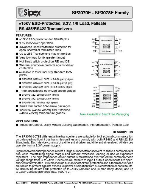
■ Three applications-optimized speed grades
■ SP3070-72E: 250kbps slew-limited
■ SP3073-75E: 500kbps slew-limited
5 GND
8 Pin Half Duplex: SP3072E, 250kbps slew limited SP3075E, 500kbps slew limited SP3078E, 16Mbps
Date: 03/28/05
SP3070E - SP3078E Family, ±15kV ESD-Protected, Failsafe RS-485/RS422 Transceivers
Operating Temperature Ranges SP307_EMN.................................................................-40ºC to +125ºC SP307_EEN ...............................................................-40ºC to +85ºC
High receiver input impedance allows a large number of transceivers to share a common data bus while maintaining signal margin and without excessive loading or use of expensive repeaters. The high impedance driver output is maintained over the entire common-mode voltage range from -7 to +12V. Receivers will failsafe to logic 1 output when inputs are open, shorted or terminated. Drivers include built-in short-circuit protection and a thermal-overload shutdown to protect against excessive power dissipation from bus contention or cable faults. All RS485 inputs are ESD protected up to ±15kV (Air-Gap and Human Body Model) and up to ±8kV Contact discharge (IEC 1000-4-2).
MTK-校准常见问题说明

WCDMA常见校准错误代码及解决措施
WCDMA FAIL 错误代码
WCDMA_FHC_AGC_CHECK_FAILED = 325,326,327,328 可能原因:WCDMA AGC异常 1. CFG中WCDMA的Path loss范围较窄 2. 接收通路异常 解决措施: 1. CFG中WCDMA的Path loss范围较窄,与研发确认调整范围 BAND1_MAX_RX_LOSS = 7.000,7.000,7.000,7.000,7.000,7.000,7.000,7.000,7.000,7.000,7.000,7.000,7.000,7.000,7.000
GSM常见校准错误代码及解决措施
GMS FAIL 错误代码
GSM_NSFT_TX_MEASURE_FAILED = 1731 GSM_EDGE_NSFT_TX_MEASURE_FAILED = 1746 可能原因: 1. GSM/EDGE TX 指标异常 GSM:Burst Match, Avg Ferr, Max Peak Perr,Switching Spectrum, Modulation Spectrum EDGE:EDGE 95P EVM,EDGE EVM PK,EDGE MAGERR PK,EDGE MAGERR RMS ,EDGE PhaseErr PK ,EDGE PhaseErr RMSPerr,Switching Spectrum, Modulation Spectrum ) 1. CFG中GSM/EDGE的指标范围较窄 解决措施: 1. 主板GSM TX 通路异常,需要维修 2. CFG中GSM/EDGE的TX指标范围较窄,与研发确认调整范围
WCDMA常见校准错误代码及解决措施
WCDMA FAIL 错误代码
- 1、下载文档前请自行甄别文档内容的完整性,平台不提供额外的编辑、内容补充、找答案等附加服务。
- 2、"仅部分预览"的文档,不可在线预览部分如存在完整性等问题,可反馈申请退款(可完整预览的文档不适用该条件!)。
- 3、如文档侵犯您的权益,请联系客服反馈,我们会尽快为您处理(人工客服工作时间:9:00-18:30)。
An Independent EvaluationofImplementing Computer Vision Functions with OpenCL on theQualcomm Adreno 420By the staff ofBerkeley Design Technology, Inc.July 2015Contents1.Introduction (2)2.Algorithm Overview (2)3.Implementation Overview (4)4.Adreno GPU OpenCL-AcceleratedImplementation (5)5.ARM CPU NEON-AcceleratedImplementation (8)6.Benefits of OpenCL Acceleration on theAdreno GPU (8)7.Conclusions (9)8.References (9)1.IntroductionComputer vision promises to bring exciting new features and user experiences to mobile devices such as smart phones, tablets and wearables. Many vision-enabled applications are already commonplace: photo-stitching techniques enable automatic generation of panoramic views from a series of images, feature detection and tracking techniques enable augmented reality experiences, and so on. And computer vision algorithms and techniques are advancing rapidly, promising to deliver many new features and applications. But computer vision algorithms tend to be very compute-intensive, threatening to bog down mobile devices’ CPU cores and memory bandwidth, and to drain their batteries.Mobile application processors increasingly include general-purpose graphics processing units: graphics processors (GPUs) capable of massively-parallel general-purpose computing. These specialized processing engines are often a great fit for computer vision algorithms, which are typically characterized by very high data parallelism (”Data parallelism” refers to the ability to distribute data among many parallel compute resources such as those available in a GPU). To implement computer vision applications, GPUs can be programmed using the open standard OpenCL language and API from the Khronos Group. For example, the Qualcomm’s Snapdragon 805 application processor includes the Adreno 420 GPU. The Adreno 420 can be programmed with OpenCL to offload vision algorithms from the CPU cores, increasing performance and reducing power consumption. In this paper we explore how BDTI used OpenCL to offload vision algorithms from the CPU to the GPU in a demonstration application, and discuss the improvements in performance and power consumption obtained using the Qualcomm Adreno GPU in this way.The BDTI Background Blur OpenCL Android application was designed to run on the Snapdragon 805 MDP tablet reference design from Intrinsyc. The application detects the largest foreground object in the camera’s view—usually the user—and displays the video with the foreground object shown unaltered, and the background shown with severe blurring applied. This functionality could be useful, for example, in a video conference call where we may want to obscure confidential information on a whiteboard behind the user, while the image of the user is seen clearly.The BDTI Background Blur OpenCL application includes two modes of operation: in the default “GPU” mode, the computationally-intensive portions of the algorithm are offloaded to the GPU using OpenCL. For comparison, a “CPU” mode is provided in which the computationally-intensive portions of the algorithm are executed on a single CPU core. This demo therefore clearly illustrates the capabilities of the Qualcomm Adreno GPU for computer vision applications.2.Algorithm OverviewThe BDTI Background Blur OpenCL application employs cutting-edge background subtraction techniques to separate foreground objects from background. The algorithm is illustrated in Figure 1.The algorithm begins with a background subtraction kernel. This kernel employs a modified version of the background subtraction algorithm described in [1]. This kernel continuously updates a model of the background, and compares each pixel in the current frame to the background model to estimate the background/foreground classification of the pixel. The background model contains multiple samples of pixel intensity and local binary pattern descriptors for each color component at each pixel position. At each pixel position, the kernel searches the samples in the background model for samples that match the color intensities and local binary pattern descriptors for the pixel position in the current frame. If sufficient matches are found, the pixel is estimated to be in the background. Otherwise it is estimated as foreground. In addition to the background/foregroundsegmentation mask, the background subtraction kernel outputs an estimated background image. When areas of the foreground closely match the background in both color and intensity, the background subtraction kernel can sometimes misclassify an entire region of foreground pixels as background. To greatly reduce this artifact, the application refines the estimated foreground mask using a proprietary method developed by BDTI and inspired by k-means clustering. The refinement compares pixels that are marked as background in the estimated mask to nearby pixels marked as foreground in the estimated mask; it marks a background pixel as foreground if it is more similar to nearby foreground pixels than it is similar to the estimated background image. This refinement procedure fills in portions of the foreground mask where the foreground pixels are too close to the background model to be correctly marked as foreground by the backgroundsubtraction kernel. The refinement method is performed in three stages:Preprocessing: in this stage the estimated foreground mask is eroded with a 3×3 structuring element to reduce false positives, and a dynamic threshold is computed for each pixel position. The dynamic threshold is used in the following stages. First-pass refinement search: in this stage, for each pixel marked as background in the estimated mask, the algorithm searches for nearby foreground pixel matches, and marks the background pixel as foreground if enough matches are found.Second-pass refinement search: this stage is identical to the previous stage, further refining the estimated foreground mask output by the previous refinement pass.Finally, the algorithm applies morphological operations, finds the contours of foreground objects, selects the largest contour, and removes all other contours from the foreground mask. TheInput FrameBlurred FrameBlurRender to DisplayCameraDisplayBackground SubtractionRefinement Preprocess Refinement Pass #1 Refinement Pass #2Contour ProcessingBlend MaskEst. Background FrameRefined MaskMaskFigure 1 BDTI Background Blur Algorithmresulting mask is used to blend the original video frame with a blurred version of the same video frame. The final refined and contour-processed mask is also passed to the background subtraction kernel along with the next video frame, where the processed mask is used to control thresholds and background model updates.To reduce computational requirements, the background subtraction and refinement kernels downsample the input frame by a factor of two horizontally, and by a factor of four vertically. This downsampling is performed by simply accessing a subset of the input pixels—a downsampled image is never physically generated in memory. Due to this downsampling of the input, the blend mask is generated at the downsampled resolution. The blend mask is passed to OpenGL-ES as a texture, and is automatically upsampled by the GPU to the original frame size during texture mapping. Because the original input image is never physically downsampled, the sharpness of the rendered foreground pixels is not impacted. Therefore, downsampling dramatically reduces computational demand with negligible impact on output quality.3.Implementation OverviewThe BDTI Background Blur OpenCL demo application is architected to realistically portray the advantages of the Adreno GPU in vision-enabled applications. The background subtraction and refinement kernels are very computationally intensive and comprise the bulk of the processing in the application. Therefore, optimizations focus on these kernels. To ensure representative performance in both the default GPU mode and in the CPU mode, thorough and reasonable optimizations are employed in both modes. Optimizations of the application’s software architecture are discussed in this section, and optimizations of the GPU and CPU implementations of the kernels are discussed in Section 4 and Section 5, respectively.When offloading computation from a CPU to a GPU, a key consideration on most hardware platforms is the need to copy data between CPU and GPU memory spaces. Memory copies introduce latency and consume power, especially for large buffers such as video frames. The BDTI Background Blur OpenCL demo application is therefore designed to minimize the need to move data between CPU and GPU memory spaces.The input video frame is needed by the GPU in both the CPU and GPU modes of operation, since the GPU renders the output in both modes. The input video is also needed by the CPU in CPU mode, but isn’t needed by the CPU when operating in GPU mode. Video frames are fetched from the camera directly into GPU memory space, eliminating the need to copy input frames in GPU mode.Figure 2 depicts the partitioning of the algorithm among processors and APIs on the Snapdragon application processor. The background subtraction and refinement kernels are implemented in OpenCL in the GPU mode, and in C using ARM NEON compiler intrinsics in the CPU mode.The contour processing portion of the algorithm is implemented on the CPU using Qualcomm’s FastCV library. Contour tracing kernels are difficult to parallelize efficiently, and therefore are not an attractive target for GPU optimization. Qualcomm’s FastCV library includes a highly optimized CPU implementation of contour tracing. In GPU mode, the refined foreground mask must be copied from GPU memory to CPU memory for contour processing. In both modes, after contour processing the resulting blend mask must be copied to GPU memory for rendering. Because the subsampled masks are only a fraction of the size of a video frame, these copies have a relatively small impact on speed and power consumption.In the GPU mode of the application, the CPU can perform contour processing in parallel with the background subtraction and refinement kernels running on the GPU. To enable this parallel operation of the CPU and GPU, the application is pipelined as illustrated in Figure 3. For each frame, background subtraction and refinement consume the frame directly from the camera, while the contour processing and rendering to the display consume a mask, an input frame, and a blurred frame from the previous frame period.The application uses OpenGL-ES to render output to the display. In addition, the application uses OpenGL-ES to render the input video frame to two textures. One is a low-resolution texture, which results in blurring of the background when this texture is interpolated back to full resolution during rendering to the display. The other texture is a full-resolution texture, which implements aone-frame delay needed due to the software pipelining of the application.4. Adreno GPU OpenCL-Accelerated ImplementationIn OpenCL, data-parallel algorithm kernels are broken down into a large number of very small “work items.” A work item typically represents the set of operations for processing a single pixel or small group of pixels. The implementation is designed to minimize —and hopefully eliminate —any dependencies between work items so that work items can execute in parallel. Programmers generally think of work items as independent parallel threads, and GPGPUs typically execute many work items in parallel. Spinning off hundreds or in some cases even thousands of work-items enables the GPU to hide memory latency.OpenCL also provides Single Instruction Multiple Data (SIMD) capabilities, with explicit support for two-, four-, eight-, and sixteen-element vectors. This enables programmers to take advantage of additional data parallelism within a work item.In the GPU mode of the BDTI Background Blur OpenCL application, background subtraction and refinement are offloaded to the Adreno GPU via OpenCL. The OpenCL code comprises three kernels: background subtraction with local binary patterns, refinement pre-process, and refinement search. The refinement search kernel is executed twice per frame. All of the OpenCL kernels are carefully refactored 1 and SIMD-optimized to expose the inherent parallelism of the algorithms and efficiently utilize the resources of the Adreno 420 GPU architecture. All three kernels operate1Code refactoring is the process of restructuring existing code without changing its external behavior.GPU/OpenGL-ESCPU/Qualcomm FastCVGPU/OpenCL Or CPU/NEONBackground Subtraction Refinement PreprocessRefinement Pass #1 Refinement Pass #2 Contour Processing Input FrameBlend Mask Delayed FrameBlurred FrameRender to TextureRender to DisplayEst.BG Frame Refined MaskCameraDisplayFigure 2 BDTI Background Blur implementation partitioningon one pixel position per work-item. Additional OpenCL implementation and optimization considerations are discussed below.Memory Footprint and Local MemoryData-intensive algorithms usually require efficient use of fast local memories for optimal performance. On a CPU, for example, algorithms can be refactored to optimize utilization of L1 caches. On a GPU, fast local memory must be explicitly managed, or else performance suffers dramatically. A collection of work-items is referred to in OpenCL parlance as a work-group, and each work-group has access to a pool of fast local memory.To minimize the impact of long DDR access latencies, each work-item copies the state and input data it needs from DDR into variables and arrays residing in local memory. The work-item then operates on this data locally. This idiom is utilized for all three OpenCL kernels in the BDTI Background Blur OpenCL application, with some important differences among the kernels described below.In the background subtraction kernel (unlike most computer vision kernel functions), each work-item accesses only a minimal amount of datafrom neighboring pixel positions. Although the background model includes many background samples per pixel position, there is little overlap in state and input data among the kernel’s work -items. Therefore, each work-item can copy its state and input data into local variables and arrays without duplicating the copies performed for neighboring pixels –thus avoiding overflowing the local memory and/or causing redundant accesses to slow DDR memory.The OpenCL code for the background subtraction kernel copies state and data from DDR into local variables, but it does not explicitly declare its local copies of input and state data as residing in local memory. For this kernel it was not necessary to manage local memory more explicitly, probably because most local variables and arrays fit in GPU registers for this kernel, and the minimal overlap with neighboring pixels means that even without more explicit techniques few DDR memory access conflicts occur. This is in contrast to the refinement pre-processing and search kernels, where more explicit memory management is required.The refinement pre-process and refinement search kernels both process a neighborhood of pixels centered on each pixel position. Therefore,BG Subtract & RefineContour ProcessingInput FrameRender to TextureRender to DisplayDelayed Frame Blurred Frame Refined MaskCameraDisplayFrame N-1BG Subtract & RefineContour ProcessingInput FrameRender to TextureRender to DisplayDelayed Frame Blurred Frame Refined Mask CameraDisplayFrame NFigure 3 Pipelining of Background Blur Implementationmost of the input data for each pixel position overlaps with the input data of neighboring pixel positions in these kernels. Explicit management of GPU local memory is needed to avoid redundant copies as each work-item copies its input into local variables and arrays.Work-items in these kernels are grouped into an eight-by-eight tile of pixel positions per work-group. Local arrays are used to store the input data required for an entire eight-by-eight tile, and are shared by all of the work-items in the respective work-group. Each work-item copies a small portion of the input data for the entire work group into the local array, and the portions fetched by work items do not overlap. After copying the data, work-items within a work-group synchronize using OpenCL’s “barrier” mechanism to ensure that all input data has been loaded before work-items proceed to perform their computations. The work-items thus cooperate to fetch overlapping inputs from slow DDR memory. This implementation technique eliminates redundant copies of data in local memory, reduces redundant accesses to DDR, and helps the GPU hide the latency of slow DDR memory accesses.Per-Pixel Pseudo-Random Number GenerationTo achieve desirable statistical properties, updates of the background model are randomized in the background subtraction kernel. Because a pseudo-random number generator updates its state with each invocation, calling a single random number generator from each work item would create a dependency as all work items attempt to access and update the same state. This dependency would block the work items from executing in parallel. Therefore, each work item includes an independent random number generator with its own state. To ensure that the random number generators for all of the work items are uncorrelated, each random number generator must be randomly seeded at initialization. The OpenCL random number generator code is based on [2].Conditional Operations and Branches GPU architectures typically require that many OpenCL work items share a single instruction stream. Multiple execution paths due to data-dependent branches or conditional operations within a work item can therefore reduce performance, oftentimes drastically. OpenCL kernels (and OpenGL shaders) are often refactored to eliminate branches.The background subtraction kernel includes many branches per pixel. However, this kernel’s performance on the Adreno GPU was about twice the performance of the CPU version without requiring refactoring to eliminate the branches. This may be due to very good correlation between the execution paths for the work items at neighboring pixel positions—when a certain branch is taken for one pixel position, it is likely for the same branch to be taken for neighboring pixels. Therefore it is likely that many work items naturally execute the same instruction stream despite the presence of branches. However, this is not always the case, and it may be possible to further improve the performance of this kernel with refactoring to eliminate some of the branches. However, in order to eliminate a branch, the refactored kernel must sometimes perform the work of both branch-taken and branch-not-taken execution paths, thus increasing the computational workload. Optimizing the background subtraction kernel further would therefore require laborious statistical analysis to balance the increase in parallelism gained from eliminating each branch against the resulting increase in computation.The refinement search kernel is explicitly refactored to eliminate branches. This kernel attempts to match each background pixel against foreground pixels in a neighborhood centered on the background pixel position. The CPU implementation of this kernel includes a branch in the kernel’s inner loop: for each pixel position the search is stopped once enough matches are found. On the GPU, however, eliminating branches is more efficient than reducing the workload by terminating the search. Therefore, the OpenCL implementation does not include the stopping condition, and always iterates through the entire inner loop.Byte-Wide Fixed-Point and Logical OperationsThe Adreno 420 GPU includes native support for 16-bit fixed-point data. To support 8-bit data, 16-bit operations are performed by the hardware, with additional operations such as sign extension sometimes added by the compiler in order to guarantee correct functionality. To minimize unnecessary operations, the OpenCL code for allthree kernels promotes some 8-bit data to 16-bit fixed-point or 32-bit floating-point data types.Additionally, the background subtraction OpenCL kernel uses a 256-entry lookup table to perform a population-count operation (the population-count operation counts the number of bits in the input word that have a value of one). 5.ARM CPU NEON-AcceleratedImplementationIn the CPU mode of the BDTI Background Blur OpenCL application, background subtraction and refinement are implemented on the CPU and refactored to efficiently utilize the CPU caches. The refinement pre-process step is split into independent operations: the erosion operation is implemented with a call to Qualcomm’s FastCV library, and the threshold computation is interleaved with the refinement search as described below.The threshold computation and two refinement search passes are pipelined on a scan-line basis, with a five scan-line delay between the first and second refinement search passes. Pipelining these functions greatly improves cache utilization and is paramount to achieving good performance on the CPU.Background subtraction and all refinement steps are carefully optimized using ARM NEON instructions to perform SIMD-parallelized operations. NEON optimizations make use of NEON’s native support for eight-bit data and native population-count instruction.6. Benefits of OpenCL Accelerationon the Adreno GPUThe BDTI Background Blur OpenCL Android application illustrates the advantages of the Adreno 420 GPU over the ARM CPU, for massively parallel algorithms programmed in OpenCL. Comp aring the application’s behavior in the GPU and CPU modes of operation reveals the performance benefit of the GPU.The computational workloads of the background subtraction and refinement kernels are data dependent. Furthermore, the computational workload’s dependencies on input data vary somewhat between the ARM NEON-optimized code and the OpenCL code. Therefore, precise comparisons of performance of the two modes can be made only for precisely defined operating conditions.BDTI has not attempted extensive, rigorous performance and power measurements on the application under carefully controlled conditions. Therefore, results measured by BDTI and presented below do not represent a comprehensive range of operating conditions and should be considered as a coarse estimate. However, BDTI has observed the performance of both the CPU and GPU modes under conditions that can be considered typical. The typical difference in performance between the GPU and CPU is striking, as discussed below.GPU vs. CPU Speed ComparisonA comparison of video display frame rates achieved under typical operating conditions in the GPU and CPU modes, respectively, is shown in Table 1. Overall, the GPU mode typically achieves a frame rate nearly two times higher than that of the CPU mode.Table 1 Frame rate comparison of GPU and CPU modesTable 2 shows the approximate time in milliseconds per invocation of the compute-intensive background subtraction and refinement kernels on the GPU and CPU. As described in Section 5 above, the two refinement search passes are tightly interleaved on the CPU, along with part of the refinement pre-processing. Therefore, it is not practical to individually profile these processing steps on the CPU. The background subtraction kernel appears to be slightly more than two times faster on the GPU compared to the CPU, although significant data-dependent timing variations occur on both the CPU and GPU. The three refinement steps combined are likewise roughly twice as fast on the GPU compared to the CPU.Contour processing requires several additional milliseconds of computation on the CPU. In GPU mode, contour processing still executes on the CPU but occurs in parallel with the OpenCL kernels running on the GPU. However, theapplication incurs some additional overhead in both modes for rendering, synchronization, and housekeeping, reducing the overall speedup of the application to slightly less than a factor of two.Table 2 Kernel duration comparison of GPU and CPU implementations, under typical conditionsNote that the CPU mode of the application uses only one of the Snapdragon processor’s ARM cores. Using two CPU cores instead of one, it is possible to achieve a frame rate roughly equivalent to that of the GPU, at the cost of slightly higher code complexity, and greatly increased power consumption.7.ConclusionsAs new computer-vision-enabled user experiences emerge in mobile, embedded, and wearable devices, computational demands will continue to rise, while size, cost, and power constraints will become more stringent. In many products, massively-parallel GPGPU implementations of key algorithm kernels will be critical to meeting application requirements. Qualcomm’s support for OpenCL on the Adreno GPU makes this possible on Snapdragon application processors.As illustrated by the BDTI Background Blur OpenCL demo application, offloading compute-intensive kernels to the Adreno 420 GPU can dramatically reduce CPU utilization in a computer-vision-enabled application, freeing CPU resources to tackle additional applications and features. Additionally, offloading compute-intensive tasks from the CPU can dramatically improve power consumption. Because of their specialized massively-parallel architectures and lower clock rates, GPUs tend to be more power-efficient than CPUs. Although BDTI did not independently measure the power consumption of the BDTI Background Blur OpenCL demo application, Qualcomm has reported that the GPU mode of the demo consumes half as much power as the CPU mode when throttling the frame rate of the GPU mode to match the highest frame rate achieved in the CPU mode.However, effective GPU programming and code optimization can be tricky. Algorithm implementations must be refactored to maximize parallelism, and conform to the memory system and core architectures of the GPU, as exemplified by the considerations discussed in this paper:∙The application must be architected to minimize memory copies between GPUand CPU memory spaces.∙GPU code must carefully manage limited fast local memory.∙Programmers must be aware of GPU core architectural characteristics, even whenprogramming in a high-level language suchas OpenCL. For example, code mustminimize the use of branches and take careto utilize the most appropriate SIMD datatypes.When implemented with best practices, computer-vision functions run efficiently on the GPU. Qualcomm’s Adreno GPU with support for OpenCL will enable vision functions in a wide range of mobile devices and applications.8.References[1] P.-L. St-Charles and G.-A. Bilodeau. Improving background subtraction using local binary similarity patterns. In Applications of Computer Vision (WACV), 2014 IEEE Computer Society Winter Conference on, 2014. 1[2] David B. Thomas. The MWC64X Random Number Generator. Retrieved from /people/dt10/research/rngs-gpu-mwc64x.htm。