Dessler_HRM12e_PPT_17
蓝色数字背景的人工智能主题PPT模板

点击输入内容点击 点击输入内容点击 点击输入内容点击 点击输入内容点击
点击输入内容点击 点击输入内容点击 点击输入内容点击 点击输入内容点击
行业ppt模板 :// . /hangye/
点击输入内容点击 点击输入内容点击 点击输入内容点击 点击输入内容点击
点击输入内容点击输入内容点击输入内容点击输入 点击输入内容点击输入内容点击输入内容点击输入 点击输入内容点击输入内容点击输入内容点击输入 点击输入内容点击输入内容点击输入内容点击输入 点击输入内容点击输入内容点击输入内容点击输入 点击输入内容点击输入内容点击输入内容点击输入 点击输入内容点击输入内容点击输入内容点击输入 点击输入内容点击输入内容点击输入内容点击输入
输入标题 TITLE HERE
点击输入内容点击输入 点击输入内容点击输入内容点击输入 点击输入内容点击输入内容点击输入
点击输入内容 点击输入内容点击输入内容 点击输入内容点击输入内容
点击输入内容 点击输入内容点击输入内容 点击输入内容点击输入内容
点击输入内容 点击输入内容点击输入内容 点击输入内容点击输入内容
点击输入内容点击输入 点击输入内容点击输入
2024
点击输入内容点击输入 点击输入内容点击输入
2026
点击输入内容点击输入 点击输入内容点击输入
2028
输入标题 TITLE H E R E
点击输入内容点击输入 点击输入内容点击输入内容点击输入 点击输入内容点击输入内容点击输入
输入标题 TITLE H E R E
R
点
O
N
击
部 E 输 入
分内 容
输入标题
TITLE HERE
点击输入内容点击输入内容点击输入内容点击输入内容点击输入内容点击输入内容 点击输入内容点击输入内容点击输入内容点击输入内容点击输入内容点击输入内容点击输入内容
思肯德测厚仪培训讲义.ppt [兼容模式]
![思肯德测厚仪培训讲义.ppt [兼容模式]](https://img.taocdn.com/s3/m/5606ccd776a20029bd642d89.png)
17
PDF 文件使用 "pdfFactory Pro" 试用版本创建
测厚仪操作及维护培训讲义
八. 机械校正完成后应将修改的参数还原 机械校正完成后应将修改的参数还原,即将下图中的红线框 内的三个勾勾上,然后点击该界面中的 然后点击该界面中的“发送参数”按钮
注意:机械校正是在没有薄膜的情况下进行的 机械校正是在没有薄膜的情况下进行的,机械校正过程中不 应让测厚仪机架移动。 18
测厚仪操作及维护培训讲义
Ø 软件界面说明
3
PDF 文件使用 "pdfFactory Pro" 试用版本创建
测厚仪操作及维护培训讲义
一. 在主界面中点击“维护” 菜单 ,出来如下界面 出来如下界面
在做mapping表前,我们需要在这里记录几个数据在该界面中可以计算出 我们需要在这里记录几个数据在该界面中可以计算出“薄膜宽度”和“偏 4 移量”的值,我们要多观察几次,确定左边和右边的值没有大的变化 确定左边和右边的值没有大的变化,膜宽已经稳定
弹出如下对话框,在“熔体宽度”栏 输入模头的宽度;在“限制宽度”栏 输入堵住的模头宽度(此模式适应于 左右堵住的模头个数一样),如果没 有堵住模头,则该值为0;在“膜宽” ” 栏输入测量薄膜的实际宽度。点击确 认。
PDF 文件使用 "pdfFactory Pro" 试用版本创建
测厚仪操作及维护培训讲义
四. 在“操作者”菜单界面下,输入测厚仪的测量值和机械卡尺的 输入测厚仪的测量值和机械卡尺的 测量值,计算薄膜的校正系数 计算薄膜的校正系数,点击“应用”投入使用
22
PDF 文件使用 "pdfFactory Pro" 试用版本创建
罗盘HIMS演示PPT

强大的在线营销工具
广州白天鹅宾馆官网 杭州布丁连锁官网 京成138连锁官网
- Hotel Information Management Solutions 酒店信息管理全面解决方案
罗盘卡酒店会员共享云联服务
Luopan Card - Hotel Membership Sharing Cloud Service
罗盘HIMS:专业管理、权限管理、个人 vs. 法人
过去数年来,针对系统灾难恢复、数据泄露控制、数据隔离和加密管理、黑客攻击、 电脑病毒等课题,罗盘实施了众多有效的技术或管理方面的措施。 譬如: 控制内部人员泄漏数据库的方法 监控内部人员的所有互联网通信 限制内部人员携带任何便携U盘 接触服务器时必须有多人在场 不允许通过网络远程访问数据库,必须去酒店机房 数据库直接由精通IT的酒店总经理控制 没有几家酒店(包括连锁酒店)可以做到上述几点! 罗盘科技可以做到! - Hotel Information Management Solutions 酒店信息管理全面解决方案
为酒店管理者节流
Cut Cost for Hoteliers
酒店完全省去运行服务器的耗电 酒店完全省去本地酒管系统维护 有效降低系统使用者的培训成本 酒店不再需要服务器的硬件投入 年节省 年节省 总节省 总节省 数千元 ~ 数万元 数千元 ~ 数万元 数千元 ~ 数十万元 数万元 ~ 数十万元
- Hotel Information Management Solutions 酒店信息管理全面解决方案
部分成功应用案例
Successful Applications
Chain Hotels 连锁酒店案例
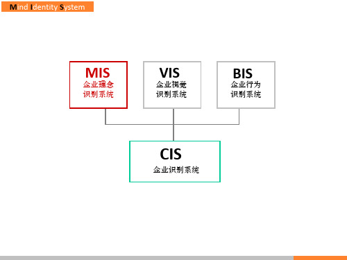
企业理念识别系统的策划MISppt课件
1、人才观 英才成就伟业、伟业造就英才。 著名的泰罗定理告诉我们:最好的管理等于最好的制度加最好的人 才。
如:海尔集团的人才观:要“赛马”而不要“相马”。 海尔认为,是不是真正的人才,不是靠上级主观即“相马”来确认 的,而是在企业经营的竞争赛场上去比赛即“赛马”脱颖而出的。 用人所长,容人所短,功不掩过。
业是没有希望的企业。美国行为学家吉格勒指出:设定一个高目标 就等于达到了目标的一部分。气魄大,方可成大业,起点高,方能 入高境界。在激烈的市场经济时代,优胜劣汰是唯一的法则,企业 不进则退,只有那些具有远大目标的企业,才能长盛不衰。
Mind Identity System
3、企业理念识别系统设计的内容
正道企业集团把自己的企业的危机观定为:兴于忧患,衰于自满。
Mind Identity System
3、企业理念识别系统设计的内容
八、 企业的文化系列价值观
6、管理观 企业文化在一定意义上讲也是一种管理文化。管理内涵丰富,涉及 企业的方方面面以及管理制度的各个方面。 华强集团的管理观:责任为大,绩效为天。表明企业以责任为中心, 以绩效为核心作为管理价值理念。责任为大,体现管理的要旨是以 责任为基础、以责任为核心。要求管理者和员工烙尽职守,尽职尽 责,做好自己的事,未尽职尽责就要承担责任,体现了管理工作的 责、权、利相结合的过程;绩效为天,体现企业的一切工作都以体 现提高绩效为核心,企业存在的目的就是要达到永续经营的目标, 就是要创造价值和价值增值。绩效为天表明管理以绩效为核心,建 立评估体系、考核制度,并以绩效为标准聘岗、晋升、计酬,让绩 效成为员工所求,进而达到永续经营的目标。
Mind ty System
3、企业理念识别系统设计的内容
霍尼韦尔SM系统ppt课件

SIS系统的结构
目前SIS的主流系统结构主要有TMR(三重化)、2oo4D(四重化) 2种。 (1)TMR结构:它将三路隔离、并行的控制系统(每路称为一个 分电路)和广泛的诊断集成在一个系统中,用三取二表决提供高 度完善、无差错,不会中断的控制。TRICON、ICS均是采用TMR结 构的系统。
(2)2oo4D结构:2oo4D系统是有2套独立并行运行的系统组成, 通讯模块负责其同步运行,当系统自诊断发现一个模块发生故障 时,CPU将强制其失效,确保其输出的正确性。同时,安全输出模 块中SMOD功能(辅助去磁方法),确保在两套系统同时故障或电 源故障时,系统输出一个故障安全信号。一个输出电路实际上是 通过四个输出电路及自诊断功能实现的。这样确保了系统的高可 靠性,高安全性及高可用性。HONEYWELL、HIMA的SIS均采用了 2004D结构。
DMR实行非冗余控制结构,每一个非冗余结构只 包含一个QPP控制单元,QPP含有冗余的处理器, 处理器与内存均为1oo2D的表决机制。
在IO配置里,每一条通路由控制器和独立的 Watchdog控制。
14
四重冗余QMR
为连续运转的过程控制提供安全防护 QMR是基于2oo4D表决机制,每一个QPP中含有双处理器
32
Watchdog看门狗
Watchdog功能 1.监视处理器运行 2.紧急停车输入(SD Input) 3.故障复位Reset
33
Watchdog结构特点
1.1oo2D结构配置 a.除对处理器等硬件进行测试外,Watchdog也要对其本身
做测试。为实现这个功能,Watchdog结构做了1oo2D结构配 置。
每一个IO Chassis最多放置18块IO卡件。
44
Dessler_HRM12e_PPT_05人力资源管理第五章

生产 规划
财务 规划
人力资源
规划
销售规划
规划
人员 人员
培训开发 规划
薪酬 规划
劳资关系 规划
安全保障 规划
规划 规划
人员 预测
招募 规划
员工甄选 规划
5–6
Copyright © 2011 Pearson Education, Inc. publishing as Prentice Hall
计划和预测
• 人员预测
确定企业需要找人填补哪些职位以及如何去
填补这些职位空缺的一个过程
• 继任计划
确定如何填补那些对于公司来说最为重要的
管职位的过程
• 预测什么?
整体人员需求 内部候选人的供给
外部候选人的供给
Copyright © 2011 Pearson Education, Inc. publishing as Prentice Hall
有效的互联网招募广告 (不必考虑空间位置) 你想帮助我们一起使这个世 界变得更加美好吗? 我们是全世界最顶级的废水 处理公司之一,从迈阿密到伦 敦再到北京,都有我们的污水 处理设施。我们正在快速成长, 需要寻找一位经验丰富的水处 理工程师加入我们的团队。如 果您有至少4至7年为废水处理 厂设计流程的工作经验,并且 致力于让我们的世界变得更加 美好,我们非常愿意收到您的 来信。该职位的薪酬水平将根 据工作经验而定,薪酬范围为 每年6.5万美元至8.5万美元之 间。有意者请密送: KimGD@。
5–7
人员需求预测
预测工具
趋势分析
比率分析
散点图
Copyright © 2011 Pearson Education, Inc. publishing as Prentice Hall
DesslerHRM12e09

主要的绩效期望: 职责或目标及绩效标准
目标1:
年中进 度
记录
对期末工作完成情
况及其有效性的评
价:通过在评价尺
度上打X来进行评
价
不强
非常
强
目标2:
目标3: 目标4
目标5:
为下一个绩效评价周期设定并 共同认可的目标:
各种问题
运用正确的绩 效评价工具
记录工作日志
达成双方认同 的绩效改进计
划
公平
表 9–3 各种绩效评价工具的主要优缺点
绩效评价工具
优点
缺点
图评价尺度法
使用简便;能为每一位员工提供一 评价标准可能会比较模糊;晕
种量化的评价结果
轮效应、居中趋势、宽大或严
格倾向、个人偏见等都可能会
成为问题
行为锚定等级评价法 能够为评价者提供一种“行为锚”;开发设计难度较大
建立行为锚定等级评价 尺度
1. 编写关键事件
2. 开发绩效维度
3. 重新分配关键事件
4. 对关键事件进行等级 评价
5. 建立最终的绩效评价 工具
行为锚定等级评价法的优 点
➢ 更精确的测量 ➢ 更清晰的标准 ➢ 反馈 ➢ 各维度相互独立 ➢ 一致性
图9–8 行为锚定等级评价尺 度的销售技能示例
销售技能 杂货店收银员:责任感 仔细且准确地完成顾客所购买物品的结账工作。在确 保按照价格精确收银以及把优惠券信息输入机器方面一丝不苟。 极其出色的绩效 9——非常仔细而迅速地检查每张优惠券的日期以确保它们是有效的。 8——在收到未挂价签的商品后,把商品装入袋子,去货架上找到相同的7商 品核对价格。 7——当顾客指出某种商品正在降价销售时能够核对促销单。 6——能够对商品准确称重,但是没有核对价签上标注的每磅价格,而是仅凭 记忆结账。 5——遇到缺价签的商品向隔壁收银台的员工询问商品的价格。 4——注意到有的商品缺了价签,向顾客询问商品的价格应该是多少。 3——没有确认价签,将属于“奢侈品”的东西当成“普通商品”出售,结果 少收40%的货款。 2——在给顾客结账时接打手机、发短信,结果导致未能对六件商品收费。 极其糟糕的绩效
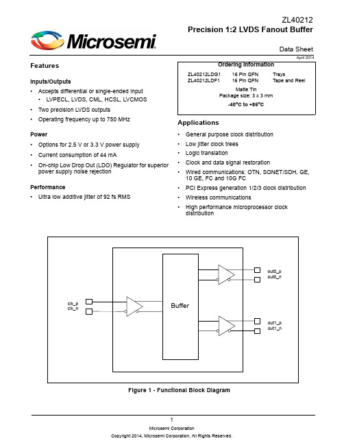
微赛米精密LVDS双倍输出缓冲器数据手册说明书
1FeaturesInputs/Outputs •Accepts differential or single-ended input •LVPECL, LVDS, CML, HCSL, LVCMOS •Two precision LVDS outputs •Operating frequency up to 750 MHzPower •Options for 2.5 V or 3.3 V power supply •Current consumption of 44 mA•On-chip Low Drop Out (LDO) Regulator for superior power supply noise rejectionPerformance •Ultra low additive jitter of 92 fs RMSApplications•General purpose clock distribution •Low jitter clock trees •Logic translation•Clock and data signal restoration•Wired communications: OTN, SONET/SDH, GE, 10 GE, FC and 10G FC•PCI Express generation 1/2/3 clock distribution •Wireless communications•High performance microprocessor clock distributionApril 2014Figure 1 - Functional Block DiagramZL40212Precision 1:2 LVDS Fanout BufferData SheetOrdering InformationZL40212LDG1 16 Pin QFN TraysZL40212LDF116 Pin QFNTape and ReelMatte TinPackage size: 3 x 3 mm-40o C to +85o CTable of ContentsFeatures . . . . . . . . . . . . . . . . . . . . . . . . . . . . . . . . . . . . . . . . . . . . . . . . . . . . . . . . . . . . . . . . . . . . . . . . . . . . . . . . . 1 Inputs/Outputs . . . . . . . . . . . . . . . . . . . . . . . . . . . . . . . . . . . . . . . . . . . . . . . . . . . . . . . . . . . . . . . . . . . . . . . . .1 Power . . . . . . . . . . . . . . . . . . . . . . . . . . . . . . . . . . . . . . . . . . . . . . . . . . . . . . . . . . . . . . . . . . . . . . . . . . . . . . . .1 Performance . . . . . . . . . . . . . . . . . . . . . . . . . . . . . . . . . . . . . . . . . . . . . . . . . . . . . . . . . . . . . . . . . . . . . . . . . . .1 Applications . . . . . . . . . . . . . . . . . . . . . . . . . . . . . . . . . . . . . . . . . . . . . . . . . . . . . . . . . . . . . . . . . . . . . . . . . . . . . 1 Change Summary . . . . . . . . . . . . . . . . . . . . . . . . . . . . . . . . . . . . . . . . . . . . . . . . . . . . . . . . . . . . . . . . . . . . . . . . . 41.0 Package Description . . . . . . . . . . . . . . . . . . . . . . . . . . . . . . . . . . . . . . . . . . . . . . . . . . . . . . . . . . . . . . . . . . . .52.0 Pin Description. . . . . . . . . . . . . . . . . . . . . . . . . . . . . . . . . . . . . . . . . . . . . . . . . . . . . . . . . . . . . . . . . . . . . . . . .53.0 Functional Description . . . . . . . . . . . . . . . . . . . . . . . . . . . . . . . . . . . . . . . . . . . . . . . . . . . . . . . . . . . . . . . . . .63.1 Clock Inputs. . . . . . . . . . . . . . . . . . . . . . . . . . . . . . . . . . . . . . . . . . . . . . . . . . . . . . . . . . . . . . . . . . . . . . . . .63.2 Clock Outputs . . . . . . . . . . . . . . . . . . . . . . . . . . . . . . . . . . . . . . . . . . . . . . . . . . . . . . . . . . . . . . . . . . . . . .113.3 Device Additive Jitter. . . . . . . . . . . . . . . . . . . . . . . . . . . . . . . . . . . . . . . . . . . . . . . . . . . . . . . . . . . . . . . . .143.4 Power Supply . . . . . . . . . . . . . . . . . . . . . . . . . . . . . . . . . . . . . . . . . . . . . . . . . . . . . . . . . . . . . . . . . . . . . .153.4.1 Sensitivity to power supply noise. . . . . . . . . . . . . . . . . . . . . . . . . . . . . . . . . . . . . . . . . . . . . . . . . . .153.4.2 Power supply filtering. . . . . . . . . . . . . . . . . . . . . . . . . . . . . . . . . . . . . . . . . . . . . . . . . . . . . . . . . . . .153.4.3 PCB layout considerations. . . . . . . . . . . . . . . . . . . . . . . . . . . . . . . . . . . . . . . . . . . . . . . . . . . . . . . .154.0 AC and DC Electrical Characteristics . . . . . . . . . . . . . . . . . . . . . . . . . . . . . . . . . . . . . . . . . . . . . . . . . . . . .165.0 Performance Characterization . . . . . . . . . . . . . . . . . . . . . . . . . . . . . . . . . . . . . . . . . . . . . . . . . . . . . . . . . . .186.0 Typical Behavior . . . . . . . . . . . . . . . . . . . . . . . . . . . . . . . . . . . . . . . . . . . . . . . . . . . . . . . . . . . . . . . . . . . . . .197.0 Package Thermal Characteristics . . . . . . . . . . . . . . . . . . . . . . . . . . . . . . . . . . . . . . . . . . . . . . . . . . . . . . . .208.0 Mechanical Drawing . . . . . . . . . . . . . . . . . . . . . . . . . . . . . . . . . . . . . . . . . . . . . . . . . . . . . . . . . . . . . . . . . . .21List of FiguresFigure 1 - Functional Block Diagram . . . . . . . . . . . . . . . . . . . . . . . . . . . . . . . . . . . . . . . . . . . . . . . . . . . . . . . . . . . . 1 Figure 2 - Pin Connections . . . . . . . . . . . . . . . . . . . . . . . . . . . . . . . . . . . . . . . . . . . . . . . . . . . . . . . . . . . . . . . . . . . 5 Figure 3 - LVPECL Input DC Coupled Thevenin Equivalent . . . . . . . . . . . . . . . . . . . . . . . . . . . . . . . . . . . . . . . . . . 6 Figure 4 - LVPECL Input DC Coupled Parallel Termination. . . . . . . . . . . . . . . . . . . . . . . . . . . . . . . . . . . . . . . . . . . 7 Figure 5 - LVPECL Input AC Coupled Termination . . . . . . . . . . . . . . . . . . . . . . . . . . . . . . . . . . . . . . . . . . . . . . . . . 7 Figure 6 - LVDS Input DC Coupled . . . . . . . . . . . . . . . . . . . . . . . . . . . . . . . . . . . . . . . . . . . . . . . . . . . . . . . . . . . . . 8 Figure 7 - LVDS Input AC Coupled . . . . . . . . . . . . . . . . . . . . . . . . . . . . . . . . . . . . . . . . . . . . . . . . . . . . . . . . . . . . . 8 Figure 8 - CML Input AC Coupled . . . . . . . . . . . . . . . . . . . . . . . . . . . . . . . . . . . . . . . . . . . . . . . . . . . . . . . . . . . . . . 9 Figure 9 - HCSL Input AC Coupled . . . . . . . . . . . . . . . . . . . . . . . . . . . . . . . . . . . . . . . . . . . . . . . . . . . . . . . . . . . . . 9 Figure 10 - CMOS Input DC Coupled Referenced to VDD/2. . . . . . . . . . . . . . . . . . . . . . . . . . . . . . . . . . . . . . . . . 10 Figure 11 - CMOS Input DC Coupled Referenced to Ground . . . . . . . . . . . . . . . . . . . . . . . . . . . . . . . . . . . . . . . . 10 Figure 12 - Simplified LVDS Output Driver. . . . . . . . . . . . . . . . . . . . . . . . . . . . . . . . . . . . . . . . . . . . . . . . . . . . . . . 11 Figure 13 - LVDS DC Coupled Termination (Internal Receiver Termination). . . . . . . . . . . . . . . . . . . . . . . . . . . . . 11 Figure 14 - LVDS DC Coupled Termination (External Receiver Termination) . . . . . . . . . . . . . . . . . . . . . . . . . . . . 12 Figure 15 - LVDS AC Coupled Termination . . . . . . . . . . . . . . . . . . . . . . . . . . . . . . . . . . . . . . . . . . . . . . . . . . . . . . 12 Figure 16 - LVDS AC Output Termination for CML Inputs . . . . . . . . . . . . . . . . . . . . . . . . . . . . . . . . . . . . . . . . . . . 13 Figure 17 - Additive Jitter. . . . . . . . . . . . . . . . . . . . . . . . . . . . . . . . . . . . . . . . . . . . . . . . . . . . . . . . . . . . . . . . . . . . 14 Figure 18 - Decoupling Connections for Power Pins. . . . . . . . . . . . . . . . . . . . . . . . . . . . . . . . . . . . . . . . . . . . . . . 15 Figure 19 - Differential Voltage Parameter. . . . . . . . . . . . . . . . . . . . . . . . . . . . . . . . . . . . . . . . . . . . . . . . . . . . . . . 17 Figure 20 - Input To Output Timing . . . . . . . . . . . . . . . . . . . . . . . . . . . . . . . . . . . . . . . . . . . . . . . . . . . . . . . . . . . . 17Change SummaryBelow are the changes from the February 2013 issue to the April 2014 issue:Page Item Change1Applications Added PCI Express clock distribution.5Pin Description Added exposed pad to Pin Description.6, 7Figure 3 and Figure 4Removed 22 ohm series resistors from Figure 3 and 4. Theseresistors are not required; however, there is no impact toperformance if the resistors are included.17Figure 19Clarification of V ID and V OD.Below are the changes from the November 2012 issue to the February 2013 issue:Page Item Change7Figure 4Changed text to indicate the circuit is not recommended forVDD_driver=2.5V.7Figure 5Changed pull-up and pull-down resistors from 2kOhm to100Ohm.11Figure 12Changed gate values to +/+ on the left and -/- on the right.The device is packaged in a 16 pin QFN1416642NCvddNCN Cc l k _pvddgndNCo u t 1_no u t 1_po u t 0_n81210o u t 0_pc l k _nN CNCgndFigure 2 - Pin Connections2.0 Pin DescriptionPin # Name Description1, 4clk_p, clk_n,Differential Input (Analog Input). Differential (or singled ended) input signals. For all input signal configuration see “Clock Inputs” on page 612, 11, 10, 9out0_p, out0_n out1_p, out1_n Differential Output (Analog Output). Differential outputs.8, 13vdd Positive Supply Voltage. 2.5 V DC or 3.3 V DC nominal.5, 16gnd Ground. 0 V.2, 3, 6, 7, 14, 15NCNo Connection. Leave unconnected.Exposed Pad Device GND.The ZL40212 is an LVDS clock fanout buffer with two identical output clock drivers capable of operating at frequencies up to 750MHz.Inputs to the ZL40212 are externally terminated to allow use of precision termination components and to allow full flexibility of input termination. The ZL40212 can accept DC coupled LVPECL or LVDS and AC coupled LVPECL, LVDS, CML or HCSL input signals; single ended input signals can also be accepted. A pin compatible device with internal termination is also available.The ZL40212 is designed to fan out low-jitter reference clocks for wired or optical communications applications while adding minimal jitter to the clock signal. An internal linear power supply regulator and bulk capacitors minimize additive jitter due to power supply noise. The device operates from 2.5V+/-5% or 3.3V+/-5% supply. Its operation is guaranteed over the industrial temperature range -40°C to +85°C.The device block diagram is shown in Figure 1; its operation is described in the following sections.3.1 Clock InputsThe ZL40212 is adaptable to support different types of differential and single-ended input signals depending on the passive components used in the input termination. The application diagrams in the following figures allow the ZL40212 to accept LVPECL, LVDS, CML, HCSL and single-ended inputs.Figure 3 - LVPECL Input DC Coupled Thevenin EquivalentFigure 4 - LVPECL Input DC Coupled Parallel TerminationFigure 5 - LVPECL Input AC Coupled TerminationFigure 6 - LVDS Input DC CoupledFigure 7 - LVDS Input AC CoupledFigure 8 - CML Input AC CoupledFigure 9 - HCSL Input AC CoupledFigure 10 - CMOS Input DC Coupled Referenced to VDD/2Figure 11 - CMOS Input DC Coupled Referenced to GroundVDD_driver R1 (kΩ)R2 (kΩ)R3 (kΩ)RA (kΩ) C (pF) 1.5 1.25 3.075open10101.81 3.8open10102.50.33 4.2open10103.30.75open4.21010Table 1 - Component Values for Single Ended Input Reference to Ground * For frequencies below 100 MHz, increase C to avoid signal integrity issues.3.2 Clock OutputsLVDS has lower signal swing than LVPECL which results in a low power consumption. A simplified diagram for the LVDS output stage is shown in Figure 12.Figure 12 - Simplified LVDS Output DriverThe methods to terminate the ZL40212 drivers are shown in the following figures.Figure 15 - LVDS AC Coupled TerminationFigure 16 - LVDS AC Output Termination for CML Inputs3.3 Device Additive JitterThe ZL40212 clock fanout buffer is not intended to filter clock jitter. The jitter performance of this type of device is characterized by its additive jitter. Additive jitter is the jitter the device would add to a hypothetical jitter-free clock as it passes through the device. The additive jitter of the ZL40212 is random and as such it is not correlated to the jitter of the input clock signal.The square of the resultant random RMS jitter at the output of the ZL40212 is equal to the sum of the squares of the various random RMS jitter sources including: input clock jitter; additive jitter of the buffer; and additive jitter due to power supply noise. There may be additional deterministic jitter sources, but they are not shown in Figure 17.Figure 17 - Additive Jitter3.4 Power SupplyThis device operates with either a 2.5V supply or 3.3V supply.3.4.1 Sensitivity to power supply noisePower supply noise from sources such as switching power supplies and high-power digital components such as FPGAs can induce additive jitter on clock buffer outputs. The ZL40212 is equipped with a low drop out (LDO) power regulator and on-chip bulk capacitors to minimize additive jitter due to power supply noise. The LDO regulator on the ZL40212 allows this device to have superior performance even in the presence of external noise sources. The on-chip regulation, recommended power supply filtering, and good PCB layout all work together to minimize the additive jitter from power supply noise.The performance of these clock buffers in the presence of power supply noise is detailed in ZLAN-403, “Power Supply Rejection in Clock Buffers” which is available from Applications Engineering.3.4.2 Power supply filteringFor optimal jitter performance, the device should be isolated from the power planes connected to its power supply pins as shown in Figure 18.•10 µF capacitors should be size 0603 or size 0805 X5R or X7R ceramic, 6.3 V minimum rating•0.1 µF capacitors should be size 0402 X5R ceramic, 6.3 V minimum rating•Capacitors should be placed next to the connected device power pins• a 0.3 Ohm resistor is recommended for the filter shown in Figure 18Figure 18 - Decoupling Connections for Power Pins3.4.3 PCB layout considerationsThe power nets in Figure 18 can be implemented either as a plane island or routed power topology without changing the overall jitter performance of the device.4.0 AC and DC Electrical CharacteristicsAbsolute Maximum Ratings*Parameter Sym.Min.Max.Units 1Supply voltage V DD_R-0.5 4.6V 2Voltage on any digital pin V PIN-0.5V DD V 3Soldering temperature T260 °C 4Storage temperature T ST-55125 °C 5Junction temperature T j125 °C 6Voltage on input pin V input V DD V 7Input capacitance each pin C p500fF * Exceeding these values may cause permanent damage. Functional operation under these conditions is not implied.* Voltages are with respect to ground (GND) unless otherwise statedRecommended Operating Conditions*Characteristics Sym.Min.Typ.Max.Units 1Supply voltage 2.5 V mode V DD25 2.375 2.5 2.625V 2Supply voltage 3.3 V mode V DD33 3.135 3.3 3.465V 3Operating temperature T A-402585°C* Voltages are with respect to ground (GND) unless otherwise statedDC Electrical Characteristics - Current ConsumptionCharacteristics Sym.Min.Typ.Max.Units Notes 1Supply current LVDS drivers - loadedI dd_load44mA(all outputs are active)DC Electrical Characteristics - Inputs and Outputs - for 2.5/3.3 V SupplyCharacteristics Sym.Min.Typ.Max.Units Notes1Differential input common modeV ICM 1.1 1.6V for 2.5 V voltageV ICM 1.1 2.0V for 3.3 V2Differential input common modevoltage3Differential input voltage V ID0.251V4LVDS output differential voltage*V OD0.250.300.40V5LVDS output common mode voltage V CM 1.1 1.25 1.375V* The VOD parameter was measured from 125 to 750 MHz.AC Electrical Characteristics* - Inputs and Outputs (see Figure 20) - for 2.5/3.3 V supply.Characteristics Sym.Min.Typ.Max.Units Notes 1Maximum Operating Frequency1/t p750MHz2Input to output clock propagation delay t pd012ns3Output to output skew t out2out50100ps4Part to part output skew t part2part80300ps5Output clock Duty Cycle degradation t PWH/ t PWL-505Percent6LVDS Output clock slew rate r sl0.55V/nsFigure 19 - Differential Voltage Parameter* Supply voltage and operating temperature are as per Recommended Operating ConditionsInputt Pt PWL t pdt PWHOutputFigure 20 - Input To Output TimingAdditive Jitter at 2.5 V*Output Frequency (MHz)Jitter MeasurementFilterTypical (fs)Notes112512 kHz - 20 MHz 1342212.512 kHz - 20 MHz 1203311.0412 kHz - 20 MHz 104442512 kHz - 20 MHz 105550012 kHz - 20 MHz 916622.0812 kHz - 20 MHz 91775012 kHz - 20 MHz92Additive Jitter at 3.3 V*Output Frequency (MHz)Jitter MeasurementFilterTypical (fs)Notes112512 kHz - 20 MHz 1352212.512 kHz - 20 MHz 1223311.0412 kHz - 20 MHz 106442512 kHz - 20 MHz 106550012 kHz - 20 MHz 946622.0812 kHz - 20 MHz 92775012 kHz - 20 MHz935.0 Performance Characterization*The values in this table were taken with an approximate input slew rate of 0.8 V/ns*The values in this table were taken with an approximate input slew rate of 0.8 V/nsAdditive Jitter from a Power Supply Tone*Carrier frequency Parameter Typical Units Notes125MHz 25 mV at 100 kHz 48fs RMS 750MHz25 mV at 100 kHz53fs RMS* The values in this table are the additive periodic jitter caused by an interfering tone typically caused by a switching power supply. For this test, measurements were taken over the full temperature and voltage range for V DD = 3.3 V. The magnitude of the interfering tone is measured at the DUT.6.0 Typical BehaviorTypical Waveform at 155.52 MHzV OD versus FrequencyPower Supply Tone Frequency versus PSRRPower Supply Tone Magnitude versus PSRRPropagation Delay versus TemperatureNote:This is for a single device. For more details see the characterization section.7.0 Package Thermal Characteristics* Proper thermal management must be practiced to ensure that T jmax is not exceeded.Thermal DataParameterSymbol Test ConditionValue UnitJunction to Ambient Thermal ResistanceΘJAStill Air 1 m/s 2 m/s 67.961.658.1oC/WJunction to Case Thermal Resistance ΘJC Still Air 44.1o C/W Junction to Board Thermal Resistance ΘJB Still Air23.2oC/WMaximum Junction Temperature*T jmax 125o C Maximum Ambient TemperatureT A85oCZL40212 Data Sheet 8.0 Mechanical Drawing21Microsemi Corporation© 2014 Microsemi Corporation. All rights reserved. Microsemi and the Microsemi logo are trademarks of Microsemi Corporation. All other trademarks and service marks are the property of their respective owners.Microsemi Corporation (NASDAQ: MSCC) offers a comprehensive portfolio of semiconductor and system solutions for communications, defense and security, aerospace and industrial markets. Products include high-performance and radiation-hardened analog mixed-signal integrated circuits, FPGAs, SoCs and ASICs; power management products; timing and synchronization devices and precise time solutions, setting the world’s standard for time; voice processing devices; RF solutions; discrete components; security technologies and scalable anti-tamper products; Power-over-Ethernet ICs and midspans; as well as custom design capabilities and services. Microsemi is headquartered in Aliso Viejo, Calif. and has approximately 3,400 employees globally. Learn more at .Microsemi Corporate Headquarters OneOne Enterprise, Aliso Viejo CA 92656 USAWithin the USA: +1 (800) 713-4113Outside the USA: +1 (949) 380-6100Sales: +1 (949) 380-6136Fax: +1 (949) 215-4996E-mail: ***************************ZL40212Information relating to products and services furnished herein by Microsemi Corporation or its subsidiaries (collectively “Microsemi”) is believed to be reliable. However, Microsemi assumes no liability for errors that may appear in this publication, or for liability otherwise arising from the application or use of any such information, product or service or for any infringement of patents or other intellectual property rights owned by third parties which may result from such application or use. Neither the supply of such information or purchase of product or service conveys any license, either express or implied, under patents or other intellectual property rights owned by Microsemi or licensed from third parties by Microsemi, whatsoever. Purchasers of products are also hereby notified that the use of product in certain ways or in combination with Microsemi, or non-Microsemi furnished goods or services may infringe patents or other intellectual property rights owned by Microsemi.This publication is issued to provide information only and (unless agreed by Microsemi in writing) may not be used, applied or reproduced for any purpose nor form part of any order or contract nor to be regarded as a representation relating to the products or services concerned. The products, their specifications, services and other information appearing in this publication are subject to change by Microsemi without notice. No warranty or guarantee express or implied is made regarding the capability, performance or suitability of any product or service. Information concerning possible methods of use is provided as a guide only and does not constitute any guarantee that such methods of use will be satisfactory in a specific piece of equipment. It is the user’s responsibility to fully determine the performance and suitability of any equipment using such information and to ensure that any publication or data used is up to date and has not been superseded. Manufacturing does not necessarily include testing of all functions or parameters. These products are not suitable for use in any medical and other products whose failure to perform may result in significant injury or death to the user. All products and materials are sold and services provided subject to Microsemi’s conditions of sale which are available on request.For more information about all Microsemi productsvisit our website atTECHNICAL DOCUMENTATION – NOT FOR RESALE。
朴素+福斯Switch Amplifier、定时器接触器区域2分类2区域0、1、2分类1、2说明书

R e l e a s e d a t e 2018-05-08 08:06D a t e o f i s s u e 2018-05-08231212_e n g .x m lZone 2Div. 23-1+101112I13+14-24 V DC23+24-II20-ConnectionAssembly•1-channel isolated barrier •24 V DC supply (Power Rail)•Dry contact or NAMUR inputs•Relay contact and transistor output•Adjustable output timer functions from 10 ms ... 60 min •Input frequency up to 80 Hz; pulse divider up to 1 kHz •Reset function•Configurable by keypad •Line fault detection (LFD)FunctionThis isolated barrier is used for intrinsic safety applications. It is a highly configurable timer that accepts a digital signal (NAMUR sensor/mechanical contact) from a hazardous area and is commonly used in applications requiring on-delay, off-delay, one-shot, or pulse lengthening.The output relay switch duration is easily adjusted, and a pulse divider function allows step-down ratios from 1:1 to 9999:1. A reset can be activated via dry contact switch and used to terminate a particular time function.The unit is easily programmed by the use of a keypad located on the front of the unit. Line fault detection of the field circuit is indicated by a red LED and through the collective error output via Power Rail.For additional information, refer to the manual and .FeaturesR e l e a s e d a t e 2018-05-08 08:06D a t e o f i s s u e 2018-05-08231212_e n g .x mlGeneral specifications Signal type Digital InputSupply Connection Power Rail or terminals 23+, 24-Rated voltage U r 20 ... 30 V DC Rated current I rapprox. 100 mA Power consumption 1.8 W InputConnection side field sideConnection Input I: terminals 1+, 3- ; input II: terminals 13+, 14-Input Iacc. to EN 60947-5-6 (NAMUR), see system description for electrical data Open circuit voltage/short-circuit current8.2 V / 10 mASwitching point/switching hysteresis 1.2 ... 2.1 mA / approx. 0.2 mAPulse duration ≥ 75 µs / 1 ms see instruction manuals; the maximum input frequency has to be observed.Input frequency 0 ... 80 Hz , pulse divider 0 ... 1 kHzLine fault detection breakage I ≤ 0.15 mA; short-circuit I > 6.5 mA Input IIresetActive/PassiveI > 4 mA/I < 1.5 mA Open circuit voltage/short-circuit current 18 V / 5 mA Pulse duration ≥ 10 ms OutputConnection side control sideConnection output I: terminals 10, 11, 12 ; output II: terminals 19+, 20-Output Isignal , Relay outputContact loading 253 V AC/ 2 A / cos φ ≥ 0.7 ; 40 V DC/ 2 A Mechanical life5 x 107 switching cycles Energized/De-energized delay approx. 20 ms / approx. 20 ms Output IIsignal , electronic unit, isolated Contact loading40 V / 50 mAEnergized/De-energized delay after rising input flank 3 ms ; after falling input flank 2 ms Signal level1-signal: (L+) -2.5 V (50 mA, short-circuit/overload proof) 0-signal: blocked output (off-state current ≤ 10 µA)Transfer characteristics Input IResolution < 0.1 % of the set value, min. 10 ms Accuracy2 msInfluence of ambient temperature 0.003 %/K (50 ppm)Galvanic isolation Input I/other circuitsreinforced insulation according to IEC/EN 61010-1, rated insulation voltage 300 V eff Output I/power supply and reset reinforced insulation according to IEC/EN 61010-1, rated insulation voltage 300 V effOutput I, II against eachother reinforced insulation according to IEC/EN 61010-1, rated insulation voltage 300 V eff Output II/power supply and collective error basic insulation according to IEC/EN 61010-1, rated insulation voltage 50 V eff Output II/resetbasic insulation according to IEC/EN 61010-1, rated insulation voltage 50 V eff Reset/power supply and collective errorfunctional insulation acc. to IEC 62103, rated insulation voltage 50 V eff Indicators/settings Display elements LEDs , display Control elements Control panel Configuration via operating buttons Labelingspace for labeling at the front Directive conformity Electromagnetic compatibilityDirective 2014/30/EU EN 61326-1:2013 (industrial locations)Low voltageDirective 2014/35/EU EN 61010-1:2010ConformityElectromagnetic compatibility NE 21:2006Degree of protection IEC 60529:2001Ambient conditions Ambient temperature -20 ... 60 °C (-4 ... 140 °F)Mechanical specifications Degree of protection IP20Connectionscrew terminalsR e l e a s e d a t e 2018-05-08 08:06D a t e o f i s s u e 2018-05-08231212_e n g .x mlMass approx. 300 gDimensions 40 x 119 x 115 mm (1.6 x 4.7 x 4.5 inch) , housing type C3Mountingon 35 mm DIN mounting rail acc. to EN 60715:2001Data for application in connection with hazardous areasEU-Type Examination Certificate TÜV 99 ATEX 1408Marking¬ II (1)G [Ex ia Ga] IIC ¬ II (1)D [Ex ia Da] IIIC ¬ I (M1) [Ex ia Ma] ISupply Maximum safe voltage U m 40 V DC (Attention! The rated voltage can be lower.)Input I terminals 1+, 3-: Ex ia Voltage U o 10.1 VCurrent I o 13.5 mAPower P o34 mW (linear characteristic)Input IIterminals 13+, 14- non-intrinsically safeMaximum safe voltage U m40 V (Attention! The rated voltage can be lower.)Output Iterminals 10, 11, 12 non-intrinsically safeContact loading 253 V AC/2 A/cos φ > 0.7; 40 V DC/2 A resistive load (TÜV 99 ATEX 1408) 50 V AC/2 A/cos φ > 0.7; 40 V DC/2 A resistive load (TÜV 02 ATEX 1885 X)Maximum safe voltage U m 253 V (Attention! The rated voltage can be lower.)Output IIterminals 19+, 20- non-intrinsically safeMaximum safe voltage U m 40 V (Attention! The rated voltage can be lower.)Certificate TÜV 02 ATEX 1885 X Marking ¬ II 3G Ex nA nC IIC T4 Gc Output IContact loading 50 V AC/2 A/cos φ > 0.7; 40 V DC/1 A resistive load Galvanic isolationInput I/other circuits safe electrical isolation acc. to IEC/EN 60079-11, voltage peak value 375 V Directive conformityDirective 2014/34/EU EN 60079-0:2012+A11:2013 , EN 60079-11:2012 , EN 60079-15:2010International approvals FM approval Control drawing 116-0305UL approval E223772IECEx approval IECEx TUN 03.0000Approved for [Ex ia Ga] IIC, [Ex ia Da] IIIC, [Ex ia Ma] IGeneral information Supplementary informationObserve the certificates, declarations of conformity, instruction manuals, and manuals where applicable. For information see .Resistive load DC Resistive load AC1max. 105 switching cyclesMaximum Switching Power of Output ContactsR e l e a s e d a t e 2018-05-08 08:06D a t e o f i s s u e 2018-05-08231212_e n g .x mlPower feed module KFD2-EB2The power feed module is used to supply the devices with 24 V DC via the Power Rail. The fuse-protected power feed module can supply up to 150individual devices depending on the power consumption of the devices. Collective error messages received from the Power Rail activate a galvanically-isolated mechanical contact.Power Rail UPR-03The Power Rail UPR-03 is a complete unit consisting of the electrical insert and an aluminium profile rail 35mm x 15mm. To make electrical contact, the devices are simply engaged.Profile Rail K-DUCT with Power RailThe profile rail K-DUCT is an aluminum profile rail with Power Rail insert and two integral cable ducts for system and field cables. Due to this assembly no additional cable guides are necessary.Power Rail and Profile Rail must not be fed via the device terminals of the individual devices!Accessories。
DEMOQE128UM

Purchase AgreementP&E Microcomputer Systems, Inc. reserves the right to make changes without further notice to any products herein to improve reliability, function, or design. P&E Microcomputer Systems, Inc. does not assume any liability arising out of the application or use of any product or circuit described herein. This software and accompanying documentation are protected by United States Copyright law and also by International Treaty provisions. Any use of this software in violation of copyright law or the terms of this agreement will be prosecuted.All the software described in this document is copyrighted by P&E Microcomputer Systems, Inc. Copyright notices have been included in the software.P&E Microcomputer Systems authorizes you to make archival copies of the software and documentation for the sole purpose of back-up and protecting your investment from loss. Under no circumstances may you copy this software or documentation for the purpose of distribution to others. Under no conditions may you remove the copyright notices from this software or documentation.This software may be used by one person on as many computers as that person uses, provided that the software is never used on two computers at the same time. P&E expects that group programming projects making use of this software will purchase a copy of the software and documentation for each user in the group. Contact P&E for volume discounts and site licensing agreements.P&E Microcomputer Systems does not assume any liability for the use of this software beyond the original purchase price of the software. In no event will P&E Microcomputer Systems be liable for additional damages, including any lost profits, lost savings or other incidental or consequential damages arising out of the use or inability to use these programs, even if P&E Microcomputer Systems has been advised of the possibility of such damage.By using this software, you accept the terms of this agreement.© 2007 P&E Microcomputer Systems, Inc. “MS-DOS” and “Windows” are registered trademarks of Microsoft Corporation. “Freescale” and “ColdFire” are registered trademarks of Freescale, Inc. “IBM” and “PowerPC” are registered trademarks of IBM corporation.P&E Microcomputer Systems, Inc.P.O. Box 2044Woburn, MA 01888617-923-0053Manual version 1.03DEMOQE User Manualii 1INTRODUCTION (1)1.1Overview ........................................................................................................11.2Package Contents..........................................................................................11.3Supported Devices.........................................................................................11.4Recommended Materials On Breaking Bit Boundaries DVD-ROM................21.5Handling Precautions . (2)2HARDWARE FEATURES...............................................................................22.1DEMOQE Base Board Features .. (2)2.2On-Board Logic Analyzer (4)2.3On-Board Virtual Serial Port (4)2.4DEMOQE Daughter Card Features (5)3SYSTEM SETUP ............................................................................................53.1Overview .. (5)3.2Operating System Requirements (5)3.3Software Setup (5)3.4Quick Startup (6)3.5Changing MCU derivative in a project under Codewarrior IDE (7)3.6Hardware Setup (9)4OPERATING MODES...................................................................................124.1Overview (12)4.2Debug Mode (12)4.3Run Mode (13)4.4External BDM Mode (13)5DEMOQE TOOLKIT PC APPLICATIONS ....................................................135.1DEMOQE Logic Analyzer Application . (13)5.2DEMOQE Terminal Application (14)5.3DEMOQE Unsecure Application (15)5.4DEMOQE Accelerometer Demo Application (16)5.5DEMOQE Serial Grapher Application (17)6DEMONSTRATION MICROCONTROLLER APPLICATIONS......................206.1Quick Start Application (20)iiiDEMOQE User Manual6.2Serial Accelerometer Application (21)7JUMPER SETTINGS....................................................................................217.1System Power.. (21)7.2RS232 Communications (23)7.3LED Display Port (25)7.4Input and Reset Switches (25)7.53-Axis Accelerometer Jumper Settings (27)7.6Buzzer (29)7.7IIC Pull-up (29)7.8Analog Input Potentiometer (30)7.9Optional External Crystal Circuitry Jumper Enable (30)7.10Optional Jumpers For Various VDD And VSS (30)8DEMOQE128 CODE DEVELOPMENT SOFTWARE...................................308.1Using CodeWarrior With The DEMOQE128. (31)8.2Using P&E Software With The DEMOQE128 (31)9TRANSITIONING TO YOUR OWN TARGET...............................................329.1Hardware Solutions At A Glance (32)9.2Working With P&E’s USB Multilink (33)9.3Working With P&E’s Cyclone PRO (34)10TROUBLESHOOTING..................................................................................3510.1DEMOQE128 Is Undetected.........................................................................3510.2CodeWarrior Installation Fails (WinDriver Error) (36)DEMOQE128 User Manual11INTRODUCTION 1.1OverviewThe DEMOQE128 is a low-cost development system designed fordemonstrating, evaluating, and debugging the Freescale MC9S08QE128 and MCF51QE128 microcontrollers. P&E’s Embedded Multilink circuitry on the DEMOQE128 board allows the processor on the DEMOQE128 to bedebugged and programmed via USB from the PC. In addition, the demo board can be powered using the USB bus.1.2Package ContentsThe DEMOQE128 package includes the following items:•DEMOQE Base Board with a MC9S08QE128 Daughter Card installed •MCF51QE128 Daughter Card •DVD Breaking Bit Boundaries - Getting Started With QE128•2-cell AAA battery package •USB Cable •Quick Start Guide •Freescale Warranty Card1.3Supported DevicesThe DEMOQE128 supports the following devices:•MC9S08QE128CLH •MCF51QE128CLH2DEMOQE128 User Manual1.4Recommended Materials On Breaking Bit Boundaries DVD-ROM•Freescale MC9S08QE128 reference manual and datasheet •Freescale MCF51QE128 reference manual and datasheet •DEMOQE Base Board Schematic •DEMOQE128 Daughter Card Schematic •DEMOQE Toolkit Applications •P&E Embedded Multilink driver installation guide and resources1.5Handling PrecautionsTake care to handle the package contents, including the DEMOQE baseboard, MC9S08QE128 daughter card, and MCF51QE128 daughter card, in a manner such as to prevent electrostatic discharge.2HARDWARE FEATURESThe DEMOQE128 is a demonstration and development system forFreescale’s MC9S08QE128 and MCF51QE128 microcontrollers. Application development is quick and easy using P&E’s Embedded Multilink circuitry and the included software tools and examples. An optional BDM port is provided to allow use of an external BDM interface such as P&E’s Cyclone PROautomated programmer or USB Multilink. The USB Multilink is functionally comparable to the DEMOQE128’s Embedded Multilink circuitry.2.1DEMOQE Base Board Features•On-board Logic Analyzer •On-board Virtual Serial Port •Asymmetrically positioned 4 8x2 male connectors for interchangeable daughter cards •P&E’s Embedded Multilink circuitry populated on the bottom •RS-232 Serial Port w/ DB9-F Connector •SCI signals connected to P&E’s Embedded Multilink through jumpers •ON/OFF Power Switch w/ LED indicatorDEMOQE128 User Manual3•A 5VDC to 12VDC power supply input barrel connector •Power Input Selection Jumpers for selecting the input voltage source:•Power Input from Embedded Multilink to LDO regulator•Power Input from DC Power Jack to LDO regulator•Regulated VDD Output at 3.0V•Regulated VDD Output at 2.1V•Power Input from Battery•Power Input from MCU_PORT connector•RESET Push Button and LED indicator w/ Enable•Optional External Crystal Circuitry Layout (not populated)•User Features:•3-axis Accelerometer w/Enable•8 User LED’s w/ Enable• 4 User Push Buttons w/ Enable• 1 Piezzo Buzzer w/ Enable•IIC Pullups w/ Enable•10K Ohm POT w/ Enable•Option Jumpers:•COM_EN for 1.8V to 4.25V RS232 Transceiver•TXD_EN for SCI_TXD to Embedded Multilink•RXD_EN for SCI_RXD to Embedded Multilink•INPUT_EN for two input channels to Embedded Multilink•Specifications:•Board Size 3.5 x 4.0•Power Input:•USB Cable: 5VDC, 500mA max•DC Power Jack: 2.5/5.5mm barrel connector, 5VDC to12VDC Center Positive4DEMOQE128 User Manual•Two AAA Battery CellsFigure 2-1: DEMOQE128 Top Component Placement2.2On-Board Logic AnalyzerThe DEMOQE board has a built-in 2-channel logic analyzer which may be used to display captured data in real-time on a host PC. The logic analyzer channels (IN0/IN1) are connected to the PTC0 and PTC1 signals on the DEMOQE board by default via the J11 jumpers. The channels may be connected to any of the processor pins by wire jumpers (not included).The DEMOQE Logic Analyzer Utility, included in the DEMOQE Toolkit on the accompanying DVD-ROM, displays the logic analyzer signals on a PC.2.3On-Board Virtual Serial PortThe DEMOQE board has a built-in virtual serial port which may be connected to the QE processor’s SCI RXD/TXD. This allows certain PC applications to be able to connect in a serial fashion to the microcontroller without the actual use of serial port hardware.The DEMOQE Terminal Window Utility, included in the DEMOQE Toolkit on the accompanying DVD-ROM, is a generic serial port utility which works withthe DEMOQE virtual serial port or actual serial port hardware.DEMOQE128 User Manual52.4DEMOQE Daughter Card Features•Four bottom-mounted asymmetrically positioned 8x2 female connectors to mate with the DEMOQE Base Board • A top-mounted MC9S08QE128CLH or MCF51QE128CLH chip3SYSTEM SETUP 3.1OverviewP&E’s Embedded Multilink driver is required to operate the DEMOQE128 using a PC. The Embedded Multilink driver should be installed with theCodeWarrior Development Studio software or from the DEMOQE Resources in the DVD-ROM before the PC is connected to the DEMOQE128.3.2Operating System RequirementsThe following are the resources required to run the CodeWarriorDevelopment Studio and the DEMOQE128:•A PC-compatible system running Windows 2000, Windows XP, or Windows Vista •128MB of available system RAM, and 1GB of available hard disk space •A DVD-ROM drive for software installation • A USB port3.3Software Setup 3.3.1Installing CodeWarrior Development StudioTo install the CodeWarrior Development Studio, insert the Breaking BitBoundaries DVD into your computer’s DVD-ROM drive. A start-up window will automatically appear. Select CodeWarrior Installation and follow the on-screen instructions.3.3.2Installing P&E ResourcesUse the DEMOQE Resources in the DVD-ROM to access and install P&E6DEMOQE128 User Manual resources for the DEMOQE128. These materials are not required foroperation. The DEMOQE Resources in the Breaking Bit Boundaries DVD-ROM contains the following supporting materials:•DEMOQE128 Embedded Multilink hardware interface driver •DEMOQE128 User Manual (this document)•DEMOQE128 Quick Start Guide •DEMOQE128 Quick Start Application Source Code •DEMOQE128 Base Board and Daughter Cards Schematics •DEMOQE128 Component Breakdown List •DEMOQE Toolkit Applications •Links to P&E Evaluation Software •Links to Freescale documentation, P&E Discussion Forums, andDEMOQE128 FAQs.3.4Quick StartupOnly a few steps are required to get the DEMOQE128 up and running:Step 1.If you do not have CodeWarrior Development Studio version 6.0installed on your computer, please install it using theaccompanying DVD-ROM. Additional information regardingCodeWarrior can be found at .Step 2.Remove the DEMOQE128 demonstration board from its anti-static pouch. The green MC9S08QE128 daughter card should beplugged into the header on the base board.Step 3.Connect the USB cable from your computer to the DEMOQE128 demonstration board. Depending on your operating system, youmay need to follow steps to install the USB driver from theDEMOQE Resources in the Breaking Bit Boundaries DVD-ROM. Once the USB cable is connected properly the green USB LED on the DEMOQE128 should illuminate.Step 4.Turn on the DEMOQE128 power switch (K6). The red Power LED should illuminate.Step 5.Press the buttons labelled PTA2, PTA3, PTD2, and PTD3. Adifferent tone should be emitted when each button is pressed, andthe corresponding LEDs labelled PTC1, PTC2, PTC3, and PTC4should illuminate. In addition, the light intensity of the LEDslabeled PTC0 and PTC5 should vary as the potentiometer isrotated.Step 6.Optionally, you may run the DEMOQE Logic Analyzer Applicationavailable in the DEMOQE toolkit on the DVD. This PC-basedapplication graphs the IN0 and IN1 signals on the DEMOQEboard. If both J11 jumpers are installed, IN0 shows PTC0 and IN1shows PTC1. Push button PTA2 and turn the potentiometer tochange these signals. This application may also be found at:/fixedlinks/demoQEtoolkit.html.Figure 3-1: DEMOQE Logic Analyzer Application3.5Changing MCU derivative in a project under Codewarrior IDE.P&E has created a sample DEMOQE128_Quick_Start firmware project. Itallows the user to utilize such DEMOQE128 peripherals as push buttons,potentiometer, LEDs and data input capture via the supplied code base.Furthermore, the same project can be used on the 9S08QE128/96/64 as wellas the MCF51QE128/96/64 by utilizing the “Change MCU/Connection”feature inside of the Codewarrior IDE. Please follow the steps below tochange the MCU type of your project. The project can then be re-compiledand programmed into the FLASH of the derivative residing on a plug-indaughter card:1.Open DEMOQE128_Quick_Start project by double clicking on .mcpfile inside of the project folder.2.Under “Project” drop down menu choose “Change MCU/Connection”option3.Under “Flexis”-> “QE128 Family”choose derivative that you areworking with. Under Connections please ensure that “P&E Multilink/ Cyclone Pro” is selected. Once desired derivative is selected click “Finish”.Figure 3-2: Device And Connection Dialog3.6Hardware Setup3.6.1First-Time ConnectionThe DEMOQE128 may be connected to a PC through a USB port.Connection steps are listed below in typical order:1.Install the required software, as described in the previous section.2.Make sure the jumpers for USB_PWR, 3V for VOLT_EN, andREG_VDD for VDD_SELECT are installed.3.Plug the USB cable A-M connector into a free USB port of the PC.4.Plug the USB cable B-M connector into the USB connector on theDEMOQE Base Board.5.The operating system will recognize P&E’s Embedded Multilink cir-cuitry and P&E’s USB to Serial circuitry. Depending on the operatingsystem, you may see the “Found New Hardware Wizard”dialog, help-ing you to install software for “PEMicro USB Multilink (i0). On Win-dows XP (SP2), the following dialog will appear:Figure 3-3: Found New Hardware Wizard Dialog (1 of 4)Select the “Install the software automatically (Recommended)” optionand click the “Next” button.6.Windows will install the driver files to your system. At the end of theinstallation, the following dialog box will appear:Figure 3-4: Found New Hardware Wizard Dialog (2 of 4) Click the “Finish” button to exit the current “Found New Hardware Wizard”.7.Depending on the operating system, you may see the “Found NewHardware Wizard”dialog again, helping you to install software for “PEMicro USB Serial Port (i1). On Windows XP (SP2), the following dialog will appear:Figure 3-5: Found New Hardware Wizard Dialog (3 of 4)Select the “Install the software automatically (Recommended)” option and click the “Next”button.8.Windows will install the driver files to your system. At the end of theinstallation, the following dialog box will appear:Figure 3-6: Found New Hardware Wizard Dialog (4 of 4)Click the “Finish” button to exit the “Found New Hardware Wizard”.If the DEMOQE128 hardware interface driver is now properly installed on yoursystem, the green USB LED on the DEMOQE Base Board should beilluminated. In addition, if you turn on the system power of the DEMOQE128you will see the red Power LED illuminate.4OPERATING MODES4.1OverviewThe DEMOQE128’s Embedded Multilink circuitry, featured hardwarecomponents, and optional external BDM header make it a versatiledevelopment tool. Below are some of the featured operating modes of theDEMOQE128.4.2Debug ModeA host communicates with the DEMOQE128 through the Embedded Multilinkcircuitry. Either the CodeWarrior Development Studio or P&E’s HCS08/CFV1software tools will work with the DEMOQE128. Please refer to Section 8 -DEMOQE128 CODE DEVELOPMENT SOFTWARE for more information.4.3Run ModeThe DEMOQE128’s rich component list empowers it to perform a variety oftasks. Once an application is developed, debugged, and programmedproperly into the QE128 internal flash memory, it can run with or withoutconnecting to a host.4.4External BDM ModeThe DEMOQE128 has an optional BDM header for debugging andprogramming the on-board QE128 device using an external BDM hardwaretool, such as P&E’s USB Multilink or Cyclone PRO. Please refer to Section 9- TRANSITIONING TO YOUR OWN TARGET for more information. A usercan take advantage of this mode to develop a target-specific QE128 systemand compare it with the DEMOQE128 when necessary.5DEMOQE TOOLKIT PC APPLICATIONSP&E provides several Windows PC-based applications which work with theDEMOQE128 board. These applications are collectively referred to as theDEMOQE Toolkit. The following applications are included in the toolkit:5.1DEMOQE Logic Analyzer ApplicationThe DEMOQE board has a built-in two-channel logic analyzer. This analyzerallows the IN0 and IN1 signals to be captured by the PC and displayed for theuser. The IN0 and IN1 signals may be connected to any of the MCU signalswhich the user would like to view. By default, they are connected to the PTC0and PTC1 pins of the MCU by jumper J11. At the time of this release, the logicanalyzer runs at a capture rate of 10khz.Figure 5-1: Logic Analyzer ApplicationThis PC-based application is used to display the logic analyzer data on thePC. The logic analyzer data is displayed in real-time and each waveform maybe paused, zoomed, and printed.If the microcontroller-based Quick Start Application is programmed into theMCU, the IN0 channel will show the PWM output on pin PTC0 whose dutycycle is controlled by the potentiometer (W1). The IN1 channel shows thePWM output on channel PTC1 which drivers the buzzer.This PC-based application is included on the DVD-ROM that accompanys theDEMOQE, and may also be found at:/fixedlinks/demoQEtoolkit.html.5.2DEMOQE Terminal ApplicationThis PC-based application acts as a standard serial port terminal applicationon the PC. It works with standard serial ports as well as the virtual serial porton the DEMOQE board. The application includes settings to adjust the COMport number, baud rate, parity, and number of data bits. There is a button totake a file on the PC and transmit it out of the serial port. There are alsodelays which are automatically inserted in the transmission output to preventoverruns. It is recommended that these defaults not be changed.Figure 5-2: DEMOQE Terminal ApplicationThe terminal window may be set for full duplex or half duplex. In full duplexmode, only received characters are displayed in the terminal window. In halfduplex mode, both transmitted and received characters are displayed.This PC-based application is included on the DVD-ROM that accompanys theDEMOQE, and may also be found at:/fixedlinks/demoQEtoolkit.html.5.3DEMOQE Unsecure ApplicationThis application allows secure CFV1 and HCS08 microcontrollers to beunsecured. The Unsecure application will erase a secure device to make itunsecure. This application works with the DEMOQE board as well as otheruser hardware connected to the PC via the USB Multilink or Cyclone PROhardware interfaces.Figure 5-3: DEMOQE Unsecure ApplicationThis PC-based application is included on the DVD-ROM that accompanys theDEMOQE, and may also be found at:/fixedlinks/demoQEtoolkit.html.5.4DEMOQE Accelerometer Demo ApplicationThis PC-based application will graph serial data output from themicrocontroller-based serial accelerometer application documented inSection 6.2 - Serial Accelerometer Application. The graphed data includesthe magnitude of the X, Y, and Z accelerometer signals, as well as the currentprocessor loading. For this application to work properly, the microcontroller-based serial accelerometer application must be programmed into themicrocontroller which is plugged into the DEMOQE board.Figure 5-4: Accelererometer Demo ApplicationThe data that is graphed may come from either the PC serial port or the virtualserial port on the DEMOQE board. The serial port of the microcontroller onthe DEMOQE board is routed to either serial port hardware or the virtual COMport based upon the setting of jumpers J6 and J7.This PC-based application is included on the DVD-ROM that accompanys theDEMOQE, and may also be found at:/fixedlinks/demoQEtoolkit.html.5.5DEMOQE Serial Grapher ApplicationThis PC-based application is a more generalized version of the accelerometerdemo application. It may be used with the microcontroller based serialaccelerometer application or customer microcontroller code which transmitsdata in the correct format. The serial graphing utility allows incoming data onthe PC serial port, or one of P&E’s virtual serial ports, to be automaticallygraphed in time or displayed upon a series of bar graphs. The virtual serialport exists on several of P&E’s embedded USB multilink designs including theDEMOQE board.This PC-based application is included on the DVD-ROM that accompanys theDEMOQE and may also be found at:/fixedlinks/demoQEtoolkit.html.All data to be displayed must be in hexadecimal format. The data can beaccepted and displayed either as incoming byte values ($00-$FF) or wordvalues ($0000-$FFFF). The data format indicates whether the data is byte orword data. The graphical components automatically size their rangedepending upon the incoming data.5.5.1Visual ComponentsThe Bar Graph has four separate bars A, B, C, and D. On each bar apercentage value is displayed which indicates the current value relative to thefull range. A byte value of $7F (max is $FF) would show up as approximately50% as would a word value of $7FFF (max is $FFFF). As can be seen in thedata formatting section, all four bars must be written at the same time. Thebars are shown here:Figure 5-5: Serial Grapher Bar GraphThe graphing component shows four waveforms X, Y, Z, and W. Themagnitude axis either has a range of $00-$FF (if byte values are incoming onthe serial port) or $0000-$FFFF (if word values are incoming). Each new setof values which comes through the serial port is added to the far right side ofthe graph and the rest of the data values move to the left. The vertical axisdisplays the incoming data as the magnitude of each waveform, and thehorizontal axis displays the number of samples. The graph has a limited size,so older samples will eventually fall off the left part of the graph. As can beseen in Section 5.5.2 - Data Format, each incoming data command affectingthe graphing component must have new data for all four waveforms. Anexample graph is shown here:Figure 5-6: Serial Grapher Graphing Component5.5.2Data FormatThe data format is broken into two sections depending upon whether theincoming data is in byte format or word format.5.5.2.1Byte Formatted DataThere are two commands which may be accepted. Both commands must endin the special characters #$0D and #$0A which are CR (carriage return) andLF (line feed). The accepted commands are:WnnZnnYnnXnnThe nn values are 00-FF and correspond in order to the data displayed on thefollowing graph lines : W, Z, Y, X.AnnBnnCnnDnnThe nn values are 00-FF and correspond in order to the data displayed on thefollowing bar graphs lines : A, B, C, D.5.5.2.2Word Formatted DataThere are three commands which may be accepted. All commands must endin the special characters #$0D and #$0A which are CR (carriage return) andLF (line feed). The accepted commands are:nnnn,nnnn,nnnn,nnnnThe nnnn values are 0000-FFFF and correspond in order to the datadisplayed on both the graph and bar graphs as follows: X/A, Y/B, Z/C, W/D.nnnn:nnnn:nnnn:nnnnThe nnnn values are 0000-FFFF and correspond in order to the datadisplayed the graphing component as follows: X, Y, Z, W.nnnn=nnnn=nnnn=nnnnThe nnnn values are 0000-FFFF and correspond in order to the datadisplayed on the bar graph component as follows: A, B, C, D.6DEMONSTRATION MICROCONTROLLER APPLICATIONS The following microcontroller applications are designed to run on the QE128processors.6.1Quick Start ApplicationThe function of the Quick Start microcontroller application is to play a differenttone and illuminate a different LED for each of the buttons which may bepressed on the DEMOQE128 board. The potentiometer controls the intensityof two LEDs on the DEMOQE128 board, via PWM signals. This applicationcomes pre-programmed into the memory of the QE128 processor.The source code for this Quick Start Application is included on the DVD-ROMincluded with the DEMOQE, and may also be found at:/fixedlinks/demoQEtoolkit.html.6.2Serial Accelerometer ApplicationThis microcontroller application samples the state of the on-board three-axisaccelerometer using on-chip A/D converter channels. This data is convertedinto ASCII characters and sent out using the serial pins of the QE128processor. These serial pins may be connected to either serial port hardwareor to P&E’s virtual serial port (which is part of the Embedded Multilink design).This connection is controlled by jumpers J6 and J7.P&E has two PC-based DEMOQE Toolkit applications which allow the serialport data generated by this application to be graphed. These are documentedin Section 5.4 - DEMOQE Accelerometer Demo Application and Section5.5 - DEMOQE Serial Grapher Application.The source code for this microcontroller based Serial AccelerometerApplication is included on the DVD-ROM included with the DEMOQE and alsomay be found at /fixedlinks/demoQEtoolkit.html.7JUMPER SETTINGS7.1System PowerThe QE128 processor may obtain its power from either the on-boardregulator, a 2-cell battery pack, or through MCU_PORT J1. The on-boardregulator obtains its input from either the Embedded Multilink circuitry or a2.5mm barrel connector. The on-board regulator can regulate the output toeither 2.1V or 3V. The DEMOQE128 is fully functional at both voltages. Powerinput and voltage selection are achieved by using 3 option headers.7.1.1J3 - Regulator Input Selection JumperJumper 3 determines whether the DEMOQE128’s on-board regulator obtainsits power from the DC power jack or from the Embedded Multilink circuitry.The regulator input selection is mutually exclusive. It prevents power inputcontention from damaging the board and the host. Figure 7-1 shows theregulator input selection details.。
德莱赛安全阀技术ppt课件

弹簧压力 F1
A2
阀瓣
A1
蒸汽压力 P2
上 调 节 环
下 调 节 环
Valve & Controls
2D2RESSER
德莱赛工业公司 阀门分部
第二代弹簧动力安全阀 (反动力安全阀)
蒸汽压力继续 升高,当蒸汽 压力大于弹簧 压力时阀门为 全开状态排量 达到最大值
全开状态: F2 = P2拻 x A2 >> F1
阀杆头球轴承与阀瓣接触点为 阀瓣承压腔最低点以上1/3R处 的 360度 承压带,使密封面承 压均匀
所有1700系列安全阀阀芯结构 完全相同,使维修备件更简单
Valve & Controls
2D5RESSER
德莱赛工业公司 阀门分部
排量和压力的关系
49,083 磅/时
97,518 磅/时
1 喷嘴
A1
弹簧压力 蒸汽反作用力
全开状态: F2 = P2拻 x A2 > F1
蒸汽压力
Valve & Controls
2D4RESSER
德莱赛工业公司 阀门分部
第三代弹簧动力安全阀
三组可调节部件,使安全阀整 定更加精确
所有1700系列安全阀均采用可 调节背压辅助回座,使回座比 压差降低到3%
真正的热适应阀瓣,使正常工 作值提高到95%整定值
德莱赛工业公司 阀门分部
再热器系统
RHO: >15% 再热器总流量
最先打开,保证足够蒸汽流过再热器,冷 却管道。
RHI+RHO:>100% 再热器总流量
采用1700系列安全阀,同汽包和过热器安 全阀结构相同。拆装方便,备件、维修经 济简单。
Valve & Controls
迅达培训ppt课件

印板间通过总线相连接 同一硬件平台实现 Miconic 10-GC 和 Miconic TX-GC 两种控制逻辑 轿顶布线由 ICE 印板完成, 轿厢信号 通过标准的通讯总线系统(LON)与控 制柜相连接
新的 Z- 系列呼梯装置 采用开关电源,实现宽电源工作范围, 并支持 4 线制和 5 线制供电 对门系统广泛支持:
T3 : ( 轿顶) DREC-U/D, ETSL, JHC, JHCT, JREC, KF,KNA, KNE, KSSC(井道及底坑) KBV, KBVG, KNE-U/D, KP, KPG
T4:机房: JRH,JHM,DRH-U/D; 厅门 KTS
T5 : 轿厢 KTC
控制柜 AS 内的印板 - BPL
用于 Miconic TX/10-GC 控制 的印板
在控制柜( AS)内的印板
ASILOG3: 是Application Specific Interface LOGic 的缩写,在本母板上装有 下列印板
•
在轿顶接线箱 OKR内的印板
– ICE : 轿厢接口板
层楼呼梯钮
层楼开关与灯
选层信号 AS 中的接点与开关
LONDAG.QD 印板
LON总线的输出印板 LONIOS16 印板有8 个 高有效的输出信号, 用于输出格雷码或连 续运行方向:
S300P Miconic TX / 10-GC概述 T-S300P 迅达中国培训中 心 02/2002
GC产品的设计理念
GC:Global Control 将是迅达电梯各个档次控制系统实现标准化和模块化的基础
H12012 低成本的OEM级和流程解决方案说明书

WITH BUILT-IN STILLING WELL
LVCN-80
$410
A sound wave is pulsed 5 times per second from the base of the transducer. The sound wave travels down the measurement tube and reflects against the process medium before returning to the receiver. The electronics measure the time of flight between the sound generation and the receipt, and translates this figure into the distance between the transmitter and the process medium below.
-20 to 60°C (-4 to 140°F) Temperature Compensation: Automatic over entire range Pressure Rating: Atmospheric Pipe Interface: 1⁄2"
Non-Conductive ˘ Conductivity Contact Non-Contact Clean Dirty
ZZZRPHJDFRXN
81,7(' 67$7(6 ZZZRPHJDFRP 7&20(*$
6WDPIRUG &7
&$1$'$ ZZZRPHJDFD /DYDO 4XHEHF 7&20(*$
德斯勒人力资源管理第14版PPT英文版 Dessler_hrm14_ ppt_04

• Conducting a job analysis • Job analysis guidelines
Copyright © 2015 Pearson Education, Inc.
4-13
Explain how to use at least three methods of collecting job analysis information, inclu4- ding interviews, questionnaires, and observation.
• Recruitment and selection
• EEO compliance 4-
• Performance appraisal
• Compensation • Training
Copyright © 2015 Pearson Education, Inc.
4-9
Conducting a Job Analysis
Copyright © 2015 Pearson Education, Inc.
4-5
Review
• Thought of as linear process
• Definition 4-
• Managing talent effectively
Copyright © 2015 Pearson Education, Inc.
Copyright © 2015 Pearson Education, Inc.
4-2
Learning Objectives
4. Explain how you would write a job description.
5. Explain how to write a job specification. 4-
- 1、下载文档前请自行甄别文档内容的完整性,平台不提供额外的编辑、内容补充、找答案等附加服务。
- 2、"仅部分预览"的文档,不可在线预览部分如存在完整性等问题,可反馈申请退款(可完整预览的文档不适用该条件!)。
- 3、如文档侵犯您的权益,请联系客服反馈,我们会尽快为您处理(人工客服工作时间:9:00-18:30)。
目分别包含哪些内容,同时还要确认这些员工到东道 国去工作时需要承担的这四类消费项目分别是什么情 况
然后企业补齐起两者之间的薪酬差距就行了——比如
员工需要额外承担的个人收入所得税或者住房开支等 等
Copyright © 2011 Pearson Education, Inc. publishing as Prentice Hall
设计全球薪酬体系的步骤
1
确定全球薪酬哲学框架 识别现有报酬体系中存在的差距 将薪酬体系系统化 根据当地薪酬情况调整薪酬政策
2
3 4 5
持续对薪酬系统进行评估
Copyright © 2011 Pearson Education, Inc. publishing as Prentice Hall
17–19
17–14
外派员工培训的趋势
• 利用外派归来的管理人员作为资源,帮助那些即将赴任的 人培养“全球性思维” • 使用软件和网络来进行这种跨文化培训 • 通过工作轮换来使海外管理人员在专业方面迅速成长 • 建立了管理技能开发中心,公司的海外高层管理人员可以 在那里进一步提高他们自己的外派技能 • 课堂培训计划为海外高层管理人员提供受教育的机会,这 些教育培训项目与他们在美国本土工作的同事所能够得到 的培训是类似的 • 持续性的、东道国国内的跨文化培训
外派管理人员的绩效评价
• 挑战
应当由谁来对外派人员的工作绩效进行评价 用什么标准来对外派人员的绩效进行衡量
• 关于改善外派管理人员绩效评价的一些建议:
1. 把握不同外派工作任务的难度等级,使绩效标准适用于不同的
情况。
2. 在对外派人员实施绩效评价的过程中,在国外当地工作的管理 3. 如果必须由母国总部的管理人员来填写书面绩效评价结果,那
Copyright © 2011 Pearson Education, Inc. publishing as Prentice Hall
17–15
外派人员的薪酬管理
• 资产负债表法
员工在母国工作时的四种主要消费项目是被关注的焦
点,即个人收入所得税、住房、商品和服务以及其他 一些自由支配的费用
企业通常要估计出员工在母国工作时消费的这四种项
进行评估 外派工作测试题库
这项测试能够鉴别出外派候选人是否具备从事海外 工作所要求的那些特征和态度。
• 现实预览
包括在未来的新工作中可能遇到的问题(例如大量的
旅行)、东道国文化的优点和问题以及东道国的国家 特征等。
Copyright © 2011 Pearson Education, Inc. publishing as Prentice Hall
• 离岸经营
让国外当地的员工去做那些原本由母国员工在公司内
完成的工作
• 离岸经营的问题
针对当地员工的有效的监督/管理机制
筛选当地员工所需的培训内容 当地的薪酬政策和用工条件
Copyright © 2011 Pearson Education, Inc. publishing as Prentice Hall 17–8
全球团队的一部分
记住,与具体方法的标准化相比,结果和胜任能
力的标准化更为重要
Copyright © 2011 Pearson Education, Inc. publishing as Prentice Hall
补贴 $32,600 3,500 33,600 0 $69,700
Copyright © 2011 Pearson Education, Inc. publishing as Prentice Hall
17–17
奖励性薪酬
• 国外服务补贴
是在正常的基本薪酬基础之上额外增加的一
部分经济补偿,其金额一般在基本薪酬的 10%到30%之内
17–10
图 17–2
有利于国际员工取得成功的五个因素及其组成部分
I. 工作知识和动机
管理能力 组织能力 想象力 创造力 行政管理技能 警觉性 责任心 勤奋刻苦 主动性和精力 强烈的动机 真诚坦率 对使命和工作的信念 持之以恒 II. 关系技能 尊重 礼貌和机智 表达敬意 善良 同情心 不武断 正直 自信
文化差异对经营结果所产生的影响
态度(包括积极的和消极的态度)是如何形成的以及态
度是如何对人的行为产生影响的
有关拟派驻国家的一些实际情况的知识
语言以及调整和适应能力
Copyright © 2011 Pearson Education, Inc. publishing as Prentice Hall
我们学到哪了…
第3 章 公司战略规划 · 我们处在什么样的行业中? · 我们的竞争基础是什么? · 为了实现我们的战略目标,我们的员工需要具备哪些特征和技能?
第4章 人力资源 规划和职 位描述
第5章 员工招募
第6,7章 面试和员 工甄选
第8 章 基于职位 要求的员 工培训
第9,10章 员工评价
第11,12,13 章 员工报酬
17–3
人力资源与企业经营国际化
• 管理者在全球化经营中面临的挑战
在全球化的基础上整合市场、产品和生产
计划
创造一种能够平衡总部集中控制与当地充
分自治之间的关系组织架构
扩展人力资源政策和系统来为海外的员工
服务
Copyright © 2011 Pearson Education, Inc. publishing as Prentice Hall
第17,18 章 全球化和 创业企业 中的人力 资源管理
第2,14,15,16章 遵守伦理道德标准、公平就业机会法律、安全规章及其他人力资源相关法律
Copyright © 2011 Pearson Education, Inc. publishing as Prentice Hall
17–2
本章学习目标
危机情况
绑架:直到雇主支付赎金之前,员工都会被扣押 为人质 敲诈勒索:威胁造成人身伤害 拘留:在没有赎金要求的情况下扣留员工 威胁破坏财产或者产品除非雇主付钱
Copyright © 2011 Pearson Education, Inc. publishing as Prentice Hall
17–4
国际人力资源管理面临的挑战
• 员工发展
赋予员工最需要的技能,不管他们身在何处
• 知识与创新思想的传播
在组织中传播最先进的知识和技能
• 在全球化的基础上识别和发展员工的才能
发现那些能够在全球化组织中高效工作的员工,并且开
发他们的能力
Copyright © 2011 Pearson Education, Inc. publishing as Prentice Hall
17–5
国家间差异如何影响人力资源管理
文化因素和伦理 道德因素
政治/法律 制度
全球化人力资源管理
经济制度
劳工关系因素
Copyright © 2011 Pearson Education, Inc. publishing as Prentice Hall
17–6
全球化人力资源实践中的异同
甄选的过程
工资和其他激励手段
全球化人力资源 管理
绩效评价的目的
培训和员工发展
Copyright © 2011 Pearson Education, Inc. publishing as Prentice Hall
17–7
国际性组织的员工配置
• 国际员工配置:母国员工还是当地员工?
外派员工
母国员工
第三国员工
• 艰苦补贴
是针对员工被派驻国外某地后,由于不得不
在一种较为艰苦的生活和工作条件下开展工 作而提供的一种补偿
• 迁移补贴
是一种典型的一次性报酬,其目的是奖励那
些从一个工作地点迁移到另外一个工作地点 去的员工
Copyright © 2011 Pearson Education, Inc. publishing as Prentice Hall 17–18
17–22
外派归国:问题及其解决思路
• 问题
确保外派员工及其家庭成员不会觉得公司不再关心他
们了
• 解决思路
为每一位外派人员及其家庭成员都配备了一名心理学
家,这些心理学家都受过归国问题方面的训练
确保外派员工感觉到他们对公司总部发生的各种事情
仍然保持着一种“在圈内”的状态
当外派人员及其家庭成员该回国时,提供正式的归国
管理价值观和国际员工配置政策
高层管理人员的价值观
民族中心主义
多国中心主义
全球中心主义
Copyright © 2011 Pearson Education, Inc. publishing as Prentice Hall
17–9
外派管理人员的甄选
• 适应性甄选
对外派人员(及其配偶)成功适应外派工作的可能性
17–11
Copyright © 2011 Pearson Education, Inc. publishing as Prentice Haபைடு நூலகம்l
外派人员的性格
配偶无法适应
个人意向
为什么外派任务 失败
很难承担海外工作 中的重大责任
家庭压力
缺乏文化适应力
Copyright © 2011 Pearson Education, Inc. publishing as Prentice Hall
1. 列举国际经营中面临的人力资源管理挑战。 2. 阐述国家间的差异会怎样对人力资源管理活动产 生影响。 3. 列举并简要描述为国际性组织配备人员的主要方 法。 4. 讨论在培训、考核国际员工以及支付薪酬时需要 牢记的一些重要问题。