Programmable cells Interfacing natural and engineered gene networks
高性能CMOS数字电路芯片说明书
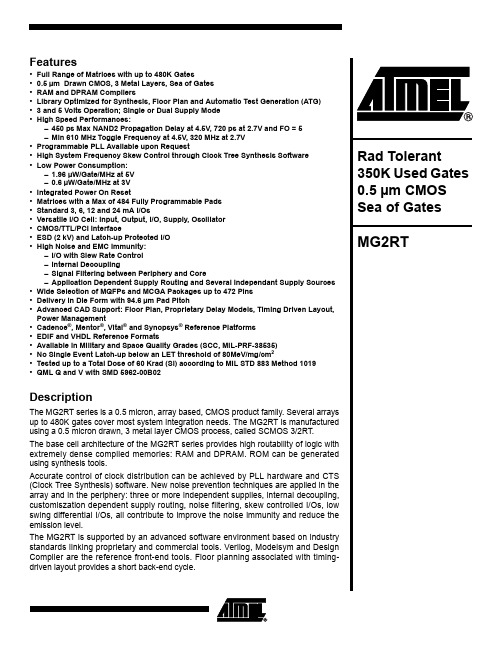
Features Array•Full Range of Matrices with up to 480K Gates•0.5 µm Drawn CMOS, 3 Metal Layers, Sea of Gates•RAM and DPRAM Compilers•Library Optimized for Synthesis, Floor Plan and Automatic Test Generation (ATG)• 3 and 5 Volts Operation; Single or Dual Supply Mode•High Speed Performances:–450 ps Max NAND2 Propagation Delay at 4.5V, 720 ps at 2.7V and FO = 5–Min 610 MHz Toggle Frequency at 4.5V, 320 MHz at 2.7V•Programmable PLL Available upon Request•High System Frequency Skew Control through Clock Tree Synthesis Software•Low Power Consumption:–1.96 µW/Gate/MHz at 5V–0.6 µW/Gate/MHz at 3V•Integrated Power On Reset•Matrices with a Max of 484 Fully Programmable Pads•Standard 3, 6, 12 and 24 mA I/Os•Versatile I/O Cell: Input, Output, I/O, Supply, Oscillator•CMOS/TTL/PCI Interface•ESD (2 kV) and Latch-up Protected I/O•High Noise and EMC Immunity:–I/O with Slew Rate Control–Internal Decoupling–Signal Filtering between Periphery and Core–Application Dependent Supply Routing and Several Independant Supply Sources •Wide Selection of MQFPs and MCGA Packages up to 472 Pins•Delivery in Die Form with 94.6 µm Pad Pitch•Advanced CAD Support: Floor Plan, Proprietary Delay Models, Timing Driven Layout, Power Management•Cadence®, Mentor®, Vital® and Synopsys® Reference Platforms•EDIF and VHDL Reference Formats•Available in Military and Space Quality Grades (SCC, MIL-PRF-38535)•No Single Event Latch-up below an LET threshold of 80MeV/mg/cm2•Tested up to a Total Dose of 60 Krad (Si) according to MIL STD 883 Method 1019•QML Q and V with SMD 5962-00B02DescriptionThe MG2RT series is a 0.5 micron, array based, CMOS product family. Several arrays up to 480K gates cover most system integration needs. The MG2RT is manufactured using a 0.5 micron drawn, 3 metal layer CMOS process, called SCMOS 3/2RT.The base cell architecture of the MG2RT series provides high routability of logic with extremely dense compiled memories: RAM and DPRAM. ROM can be generated using synthesis tools.Accurate control of clock distribution can be achieved by PLL hardware and CTS (Clock Tree Synthesis) software. New noise prevention techniques are applied in the array and in the periphery: three or more independent supplies, internal decoupling, customiszation dependent supply routing, noise filtering, skew controlled I/Os, low swing differential I/Os, all contribute to improve the noise immunity and reduce the emission level.The MG2RT is supported by an advanced software environment based on industry standards linking proprietary and commercial tools. Verilog, Modelsym and Design Compiler are the reference front-end tools. Floor planning associated with timing-driven layout provides a short back-end cycle.24115L–AERO–06/05MG2RTThe MG2RT library allows straight forward migration from the MG1RT and MG1 Sea of Gates.A netlist based on this library can be simulated as either MG2RT or MG2RTP. It can also be sim-ulated as MG2 provided there are no SEU hardened cells.Note:Not available for new designs.LibrariesThe MG2RT cell library has been designed to take full advantage of the features offered by both logic and test synthesis tools.Design testability is assured by the full support of SCAN, JTAG (IEEE 1149) and BIST methodologies.More complex macro functions are available in VHDL, such as Two-wire Interface (TWI), UART,Timer.Block GeneratorsBlock generators are used to create a customer specific simulation model and metallisation pat-tern for regular functions like RAM and DPRAM. The basic cell architecture allows one bit per cell for RAM and DPRAM. The main characteristics of these generators are summarised below.Table 1. List of Available MG2RT MatricesType Total Gates Typical UsableGatesTotal PadsMaximum Programmable I/OMG2044E (1)4461631200173150MG2091E 9146464000237214MG2194E (1)193800135600333310MG2265E 264375185000385362MG2360E (1)361680253100445422MG2480E481143336800507484Function Maximum Size (bits)Bits/WordTypical Characteristics (16 Kbits) at 5VAccess Time (ns)Used CellsRAM 32K 1-368.620K DPRAM32K1-369.223K34115L–AERO–06/05MG2RTI/O Buffer InterfacingI/O Flexibility All I/O buffers may be configured as input, output, bi-directional, oscillator or supply. A level translator is located close to each buffer.InputsInput buffers with CMOS or TTL thresholds are non-inverting and feature versions with and with-out hysteresis. The CMOS and TTL input buffers may incorporate pull-up or pull down terminators. For special purposes, a buffer allowing direct input to the matrix core is available. OutputsSeveral kinds of CMOS and TTL output drivers are offered: fast buffers with 3, 6, 12 and 24 mA drive at 5V, low noise buffers with 12 mA drive at 5V.Clock Generation and PLLClock GenerationAtmel offers 6 different types of oscillators: 4 high frequency crystal oscillators and 2 RC oscilla-tors. For all devices, the mark-space ratio is better than 40/60 and the start-up time less than 10ms.PLLContact factory.Oscillators Frequency (MHz)Typical Consumption (mA)Max 5V Max 3V5V 3V Xtal 7M 127 1.20.4Xtal 20M 2817 2.50.8Xtal 50M 704072Xtal 100M 13075165RC 10M 101021RC 32M323231.544115L–AERO–06/05MG2RTPower Supply and Noise ProtectionThe speed and density of the SCMOS3/2RT technology cause large switching current spikes for example when: •either 16 high current output buffers switch simultaneously,•or 10% of the 480,000 gates are switching within a window of 1 ns.Sharp edges and high currents cause some parisitic elements in the packaging to become sig-nificant. In this frequency range, the package inductance and series resistance should be taken into account. It is known that an inductor slows down the settling time of the current and causes voltage drops on the power supply lines. These drops can affect the behavior of the circuit itself or disturb the external application (ground bounce).In order to improve the noise immunity of the MG core matrix, several mechanisms have been implemented inside the MG arrays. Two kinds of protection have been added: one to limit the I/O buffer switching noise and the other to protect the I/O buffers against the switching noise coming from the matrix.I/O Buffers Switching ProtectionThree features are implemented to limit the noise generated by the switching current: •The power supplies of the input and output buffers are separated.•The rise and fall times of the output buffers can be controlled by an internal regulator. •A design rule concerning the number of buffers connected on the same power supply line has been imposed.Matrix Switching Current Protection This noise disturbance is caused by a large number of gates switching simultaneously. To allow this without impacting the functionality of the circuit, three new features have been added:•Decoupling capacitors are integrated directly on the silicon to reduce the power supply drop.•A power supply network has been implemented in the matrix. This solution reduces the number of parasitic elements such as inductance and resistance and constitutes an artificial VDD and Ground plane. One mesh of the network supplies approximately 150 cells. •A low pass filter has been added between the matrix and the input to the output buffer. This limits the transmission of the noise coming from the ground or the VDD supply of the matrix to the external world via the output buffers.54115L–AERO–06/05MG2RTPackagingAtmel offers a wide range of packaging options which are listed below:Note: 1.Contact Atmel local design centers to check the availability of the matrix/package combination.Package Type (1)Pinsmin/max Lead Spacing(mils)MQFP100132196256352252525202064115L–AERO–06/05MG2RTDesign Flows and ToolsDesign Flows and Modes A generic design flow for an MG2RT array is illustrated below.A top down design methodology is proposed which starts with high level system description andis refined in successive design steps. At each step, structural verification is performed whichincludes the following tasks: •Gate level logic simulation and comparison with high level simulation results.•Design and test rules check.•Power consumption analysis.•Timing analysis (only after floor plan).The main design stages are:•System specification, preferably in VHDL form.•Functional description at RTL level.•Logic synthesis.•Floor planning and bonding diagram generation.•Test/Scan insertion, ATG and/or fault simulation.•Physical cell placement, JTAG insertion and clock tree synthesis.•Routing.To meet the various requirements of designers, several interface levels between the customer and Atmel are possible.For each of the possible design modes a review meeting is required for data transfer from the user to Atmel. In all cases the final routing and verifications are performed by Atmel.The design acceptance is formalized by a design review which authorizes Atmel to proceed with sample manufacturing.74115L–AERO–06/05MG2RTFigure 1. MG2RT Design FlowGate Level System SpecificationsRTL SimulationLogic synthesisFloor Plan Bonding diagramScan insertionATG and Fault SimulationJTAG insertion Clock Tree SynthesisRouting + ExtractBackannotated SimulationSign-off Samples Manufacturing and TestPlacementSimulation84115L–AERO–06/05MG2RTDesign Tool and Design Kits (DK)The basic content of a design kit is described in the table below.The interface formats to and from Atmel rely on IEEE or industry standard: •VHDL for functional descriptions •VHDL or EDIF for netlists•Tabular, log or .VCD for simulation results •SDF (VITAL format) and SPF for back annotation •LEF and DEF for physical floor plan informationThe design kits supported for several commercial tools are listed below.Design Kit Support•Cadence/Verilog (RTL and gate), Logic Design Planner•Mentor/Modelsim (RTL and gate), Velocity, BSD Architect, Flex Test •Synopsys, Design Compiler, PrimeTime •VitalTable 2. Design Kit DescriptionDesign Tool or library Atmel Software Name Third Party ToolsDesign manual and libraries (1)Synthesis library(1)Gate level simulation library (1)Design rules analyser STAR Power consumption analyser COMETFloor plan library (1)Timing analyser library (1)Package and bonding software PIMScan path and JTAG insertion (1)ATG and fault simulation library(1)Note: 1.Refer to “Design kits cross reference tables” ATD-TS-WF-R018194115L–AERO–06/05MG2RTElectrical CharacteristicsAbsolute Maximum RatingsDC CharacteristicsAmbient temperature under bias (TA)Military......................................................-55 to +125°C Junction temperature....................................TJ < 175°C Storage temperature.................................-65 to +150°C TTL/CMOS:Supply voltage VDD...................................-0.5V to +7V I/O voltage......................................-0.5V to VDD + 0.5VNote:Stresses above those listed may cause permanent damage to the device. Exposure to absolute maxi-mum rating conditions for extended period may affect device reliability.Table 3. DC Characteristics - Specified at VDD = +5V ± 10%SymbolParameterMinTypMax UnitConditionsVILInput LOW voltage (3)CMOS input TTL input001.50.8VVIHInput HIGH voltage (3)CMOS input TTL input3.52.2VDD VDD V VOL Output LOW voltage 0.4V IOL =24, 12, 6, 3 mA (1)VOHOutput HIGH voltage3.9VIOL =-24, -12, -6, -3 mA (1)VT+Schmitt trigger positive threshold CMOS input TTL input3.61.8VVT-Schmitt trigger negative threshold CMOS input TTL input1.21.0VDelta V CMOS hysteresis 25°C/5V TTL hysteresis 25°C/5V 1.90.6VILInput leakage No pull up/down Pull up Pull down-5-5579-69125+5-120330µA µA µA IOZ3-State Output Leakage current -5+5µAIOSOutput Short circuit currentIOSN IOSP90180270540mABOUT3BOUT6BOUT12BOUT24ICCSB Leakage current per cell 1.010.0nA ICCOPOperating current per cell0.390.58µA/MHz/gateNotes:1.According buffer: Bout24, Bout12, Bout6, Bout3.2.Supplied as a design limit but not guaranteed or tested. No more than one output at a time may be shorted for a maximumduration of 10 seconds.3.Without Schmitt trigger.104115L–AERO–06/05MG2RTTable 4. DC Characteristics - Specified at VDD = +3V ± 0.3VSymbolParameterMinTypMax UnitConditionsVILInput LOW voltage (3)LVCMOS input LVTTL input 000.3 VDD 0.8VVIH Input HIGH voltage (3)LVCMOS input LVTTL input 0.7 VDD 2.0VDD VDDVVOLOutput LOW voltage LVTTL0.4VIOL=12, 6, 3, 1.5 mA (1)VOHOutput high voltage LVTTL2.4VIOH= -8, -4, -2, -1 mA (1)VT+Schmitt trigger positive threshold LVCMOS input LVTTL input2.21.2VVT-Schmitt trigger negative threshold LVCMOS input LVTTL input0.90.8VDelta V CMOS hysteresis 25°C/3V TTL hysteresis 25°C/3V 0.80.2VILInput leakage No pull up/down Pull up Pull down-1-20322442+1-60150µA µA µA IOZ3-State Output Leakage current ±1µAIOSOutput Short circuit currentIOSN IOSP90180270540mABOUT3BOUT6BOUT12BOUT24ICCSB Leakage current per cell 0.65nA ICCOPOperating current per cell0.20.25µA/MHz/gateNotes:1.According buffer: Bout24, Bout12, Bout6, Bout3.2.Supplied as a design limit but not guaranteed or tested. No more than one output at a time may be shorted for a maximumduration of 10 seconds.3.Without Schmitt trigger.114115L–AERO–06/05MG2RTAC CharacteristicsTable 5. AC Characteristics - TJ = 25°C, Process typical (all values in ns)Buffer DescriptionLoad TransitionVDD5V 3V BOUT12Output buffer with 12 mA drive60 pfTplh2.533.91Tphl 2.76 3.64BOUT3Output buffer with 3 mA drive60 pfTplh4.637.22Tphl 4.86 6.36BOUTQLow noise output buffer with 12 mA drive60 pfTplh2.974.48Tphl 4.36 6.24B3STA33-state output buffer with 3 mA drive60 pfTplh4.737.35Tphl 4.89 6.44B3STA123-state output buffer with 12 mA drive60 pfTplh2.644.07Tphl 2.79 3.72B3STAQLow noise 3-state output buffer with 12 mA drive60 pfTplh3.014.61Tphl4.426.34124115L–AERO–06/05MG2RTTable 6. AC Characteristics - TJ = 25°C, Process typical (all values in ns)Cell Description Load TransitionVDD5V 3V BINCMOSCMOS input buffer15 fanTplh0.771.14Tphl 0.75 1.06BINTTLTTL input buffer16 fanTplh0.91.31Tphl 0.7 1.1INVInverter12 fanTplh0.520.8Tphl 0.420.53NAND22 - input NAND12 fanTplh0.731.11Tphl 0.660.9FDFFD flip-flop, Clk to Q8 fanTplh 0.8 1.21Tphl0.681.02Ts 0.330.44Th -0.12-0.24BUF4XHigh drive internal buffer51 fanTplh0.761.1Tphl 0.580.81NOR22-Input NOR gate8 fanTplh0.651.08Tphl 0.370.45OAI224-input OR AND INVERT gate8 fanTplh0.681.14Tphl 0.420.54 OSFFD flip-flop with scan input, Clk to Q8 fanTplh 0.83 1.23Tphl1.001.38Ts 0.560.8Th-0.34-0.64115L–AERO–06/05© Atmel Corporation 2005. All rights reserved. Atmel ®, logo and combinations thereof, are registered trademarks, and Everywhere You Are ®are the trademarks of Atmel Corporation or its subsidiaries. Other terms and product names may be trademarks of others.Disclaimer: The information in this document is provided in connection with Atmel products. No license, express or implied, by estoppel or otherwise,to any intellectual property right is granted by this document or in connection with the sale of Atmel products. EXCEPT AS SET FORTH IN ATMEL’S TERMS AND CONDI-TIONS OF SALE LOCATED ON ATMEL’S WEB SITE, ATMEL ASSUMES NO LIABILITY WHATSOEVER AND DISCLAIMS ANY EXPRESS, IMPLIED OR STATUTORY WARRANTY RELATING TO ITS PRODUCTS INCLUDING, BUT NOT LIMITED TO, THE IMPLIED WARRANTY OF MERCHANTABILITY, FITNESS FOR A PARTICULAR PURPOSE, OR NON-INFRINGEMENT. IN NO EVENT SHALL ATMEL BE LIABLE FOR ANY DIRECT, INDIRECT, CONSEQUENTIAL, PUNITIVE, SPECIAL OR INCIDEN-TAL DAMAGES (INCLUDING, WITHOUT LIMITATION, DAMAGES FOR LOSS OF PROFITS, BUSINESS INTERRUPTION, OR LOSS OF INFORMATION) ARISING OUT OF THE USE OR INABILITY TO USE THIS DOCUMENT, EVEN IF ATMEL HAS BEEN ADVISED OF THE POSSIBILITY OF SUCH DAMAGES. Atmel makes no representations or warranties with respect to the accuracy or completeness of the contents of this document and reserves the right to make changes to specifications and product descriptions at any time without notice. Atmel does not make any commitment to update the information contained herein. Unless specifically provided otherwise, Atmel products are not suitable for, and shall not be used in, automotive applications. Atmel’s products are not intended, authorized, or warranted for use as components in applications intended to support or sustain life.Atmel CorporationAtmel Operations2325 Orchard Parkway San Jose, CA 95131, USA Tel: 1(408) 441-0311Fax: 1(408) 487-2600Regional HeadquartersEuropeAtmel SarlRoute des Arsenaux 41Case Postale 80CH-1705 Fribourg SwitzerlandTel: (41) 26-426-5555Fax: (41) 26-426-5500AsiaRoom 1219Chinachem Golden Plaza 77 Mody Road Tsimshatsui East Kowloon Hong KongTel: (852) 2721-9778Fax: (852) 2722-1369Japan9F, Tonetsu Shinkawa Bldg.1-24-8 ShinkawaChuo-ku, Tokyo 104-0033JapanTel: (81) 3-3523-3551Fax: (81) 3-3523-7581Memory2325 Orchard Parkway San Jose, CA 95131, USA Tel: 1(408) 441-0311Fax: 1(408) 436-4314Microcontrollers2325 Orchard Parkway San Jose, CA 95131, USA Tel: 1(408) 441-0311Fax: 1(408) 436-4314La Chantrerie BP 7060244306 Nantes Cedex 3, France Tel: (33) 2-40-18-18-18Fax: (33) 2-40-18-19-60ASIC/ASSP/Smart CardsZone Industrielle13106 Rousset Cedex, France Tel: (33) 4-42-53-60-00Fax: (33) 4-42-53-60-011150 East Cheyenne Mtn. Blvd.Colorado Springs, CO 80906, USA Tel: 1(719) 576-3300Fax: 1(719) 540-1759Scottish Enterprise Technology Park Maxwell BuildingEast Kilbride G75 0QR, Scotland Tel: (44) 1355-803-000Fax: (44) 1355-242-743RF/AutomotiveTheresienstrasse 2Postfach 353574025 Heilbronn, Germany Tel: (49) 71-31-67-0Fax: (49) 71-31-67-23401150 East Cheyenne Mtn. Blvd.Colorado Springs, CO 80906, USA Tel: 1(719) 576-3300Fax: 1(719) 540-1759Biometrics/Imaging/Hi-Rel MPU/High Speed Converters/RF DatacomAvenue de Rochepleine BP 12338521 Saint-Egreve Cedex, France Tel: (33) 4-76-58-30-00Fax: (33) 4-76-58-34-80Literature Requests/literature。
电子信息工程专业英语专业术语速查表5.0
AA/D abbr. Analog-to-Digital 模数转换16, 17AC abbr. alternating current 交流电5AC analysis 交流分析5 accumulator [ə'kjuːmjʊleɪtə] n.累加器17 accuracy [ˈækjʊrəsi] n.精度6 acquisition time 采集时间16 activate [ˈæktɪveɪt] vt. 激活3active [ˈæktɪv] adj.有源的4, 18 actuator [ˈæktjʊeɪtə] n.激励器4ADC abbr. analog-to-digital converter 模数转换器6, 18 addition [əˈdɪʃən] n. 加法3 address generator 地址产生器17 address latch 地址锁存器3 address pointer 地址指针2 addressing mode 寻址模式26 ADSL abbr. Asymmetrical Digital Subscriber Loop 非对称数字用户线21AFG abbr. Arbitrary Function Generator 任意函数发生器28 algorithm ['ælgərɪðəm] n. 算法27 aliasing ['eɪlɪəsiŋ] n.混叠16ALU abbr. Arithmetic Logic Unit 算术逻辑单元3 amplifier [ˈæmplɪˌfaɪə] n. 放大器4 analog interfacing模拟接口(技术)6 angular [ˈæŋɡjələ] adj.角度的5 angular frequency 角频率5 annotation [ænə'teɪʃən] n.标注15 antenna [ænˈtenə] n.天线10anti-aliasing filter 抗混叠滤波器6, 16 array [ə'reɪ] n.数组26ASIC abbr. Application-Specific Integrated Circuit 专用集成电路13, 14, 15, 16, 25专用集成电路assembler [əˈsemblə] n. 汇编器3 assembly language 汇编语言3 ASSP abbr. Application-Specific Standard Part 专用标准部件14, 25 asynchronous [ə'sɪŋkrənəs] adj.异步的13 attenuator [ə'tenjʊeɪtə] n. 衰减器29 audio [ˈɔːdiəʊ] adj.音频的6 automatic variable 自动变量26AWG abbr. Arbitrary Waveform Generator 任意波形发生器28axis [ˈæksɪs] n. 坐标轴5Bbackplane [ˈbækˌpleɪn] n. 背板;底板9 backward compatible 向下兼容21 bandwidth ['bændˌwɪdθ] n.带宽6第 1 页共15 页bar graph 柱图22base band 基带6base station 基站10, 21battery [ˈbætəri] n. 电池7, 12baud [bɔːd] n.波特21Bessel filter 贝塞耳滤波器19biased [ˈbaɪəst] adj.加偏压的7bill of materials 材料单25binary number 二进制数3BIOS [ˈbaɪɒs] abbr. Basic Input Output System 基本输入输出系统3bipolar [baɪˈpəʊlə] adj.双极性的2bit pattern 位模式3bit vector 位向量26block diagram 方框图6block diagram 框图19BNC abbr. bayonet Neill–Concelman BNC连接器9Bode plot 伯德图5bond [bɒnd] n.接头9boot sector 引导扇区3branch instruction 分支指令26缓存器;;缓存区3, 10 buffer [ˈbʌfə] n. 缓存器bunching ['bʌntʃiŋ] n.聚束19bus interface 总线接口16Ccable ['keɪbl] n.电缆12cache [kæʃ] n.高速缓存2CAD abbr. Computer Aided Design 计算机辅助设计13, 18calculation-intensive algorithm 运算密集型算法17CAM [kæm] abbr. Content Addressable Memory 内容寻址存储器2capacitance [kəˈpæsɪtəns] n. 电容(值)5capacitive [kəˈpæsɪtɪv] adj. 容性的9capacitor [kəˈpæsɪtə] n.电容器2, 5capacity [kə'pæsɪtɪ ] n.容量10capture ['kæptʃə] vt. 输入,记录13carrier wave 载波24carry bit 进位位3cascade [kæsˈkeɪd] n.级联5cathode ['kæθəʊd] n. 阴极29CB abbr. Citizen's Band 民用波段10CCD abbr. Charge Coupled Device 电荷耦合器件18, 23CD abbr. Compact Disc 光盘12, 13cellular [ˈseljʊlə] n.使用蜂窝技术的6channel [ˈtʃænəl] n.信道6第 2 页共15 页characteristic frequency 特征频率5 charge pump 电荷泵8 Chebyshev Type 1 filter 契比雪夫I型滤波器18 chip [tʃɪp] n. 芯片1 chip rate 码片速率21 chrominance [ˈkrəʊmɪnəns] n.色度24 circuit [ˈsɜːkɪt] n. 电路1 circuit board 电路板1 circuitry [ˈsɜːkɪtri] n. 电路2, 4, 6 circular [ˈsɜːkjʊlə] adj. 圆形的5 circular buffer 循环缓冲区17 class [klɑːs] n.类26 clock cycle 时钟周期3 clock generator 时钟发生器8 clock rate 时钟速率9 CMOS abbr. complementary metal-oxide-semiconductor 互补金属氧化物半导体2, 9, 12, 23 coding theory 编码理论11 comparator [kəmˈpærətə] n.比较器2, 6 compatibility [kəmˌpætɪ'bɪlɪtɪ] n. 兼容性16 compiler [kəmˈpaɪlə] n.编译器3, 26 complex plane 复平面5 component [kəmˈpəʊnənt] n. 元器件;组件;部件1 concurrent [kən'kʌrənt] adj.并发的15 concurrent process 并发进程26 conductivity [kɒndʌkˈtɪvɪti] n.导电性7 conjugate [ˈkɒndʒʊɡeɪt] adj.共轭的5 converter [kənˈvɜːtə] n. 整流器7 converter resolution 转换器分辨率6 coordinate [kəʊˈɔːdɪnət] n. 坐标5 cordless phone 无绳电话10 counter [ˈkaʊntə] n. 计数器3 coupling [ˈkʌplɪŋ] n.耦合9 CPU abbr. central processing unit中央处理器1, 12程序))25, 27交叉编译器((程序cross-compiler 交叉编译器crosstalk [ˈkrɒsˌtɔːk] n.串扰9 crowbar [ˈkrəʊˌbɑː] n. 短路器7 CRT abbr. Cathode Ray Tube 阴极射线管29 cryptography [krɪp'tɒgrəfɪ] n. 密码学14 crystal [ˈkrɪstəl] n.晶体8, 18 CT abbr. Computed Tomography 计算机层析成像22 current source 电流源4 cutoff [ˈkʌtɒf] n.截止7 cutoff frequency 截止频率18第 3 页共15 页DD/A abbr. Digital-to-Analog 数模转换16, 17 DAC abbr. Digital-to-Analog Converter 数模转换器18 damping [ˈdæmpɪŋ] n.幅度衰减5 data acquisition 数据采集30 data compression 数据压缩18 data converter 数据转换器6 data processing 数据处理14 data rate 数据率19 data sheet 数据手册4, 6 dB abbr. decibel [ˈdesɪˌbel] 分贝5 DC abbr. direct current 直流电5 DCT abbr. Discrete Cosine Transform 离散余弦变换22 debug [diː'bʌg] vt.调试28 debugger [diː'bʌgə] n. 调试程序27 decimation [desɪ'meɪʃən] n.抽取6 declaration [deklə'reɪʃən] n.声明15 decoder [diːˈkəʊdə] n. 译码器3 delta modulation 增量调制(∆调制)11 denominator [dɪˈnɒmɪˌneɪtə] n.分母5 density [ˈdensəti] n. 密度2 design flow 设计流程13 design specification 设计规格28 desired signal 期望信号28 detector [dɪˈtektə] n.检波器8 deviation [ˌdiːviˈeɪʃən] n. 偏差8 device driver 设备驱动程序27 DG abbr. Data Generator 数据发生器28 dial tone 拨号音10 differentiation [ˌdɪfərenʃiˈeɪʃən] n. 微分4 digital [ˈdɪdʒɪtəl] adj.数字的1 digital cellular phone 数字蜂窝电话6 digital circuit 数字电路2 digital filtering 数字滤波6 digitization [ˌdɪdʒɪtɪ'zeʃən] n. 数字化16 diode [ˈdaɪəʊd] n. 二极管7 discrete [dɪ'skriːt] adj.离散的,分立的1, 13 discrete component 分立元件3 disk drive head 磁盘驱动器磁头18 dissipate [ˈdɪsɪˌpeɪt] vi.耗散7 distortion [dɪ'stɔːʃən] n.畸变28 division [dɪˈvɪʒən] n. 除法3 DMM abbr. digital multimeter 数字多用表28第 4 页共15 页Dolby Stereo 杜比立体声19 don't care 无关项15 downstream ['daʊn'striːm] n.下行比特流11 DRAM abbr. Dynamic Random Access Memory 动态随机存取存储器2 drive [draɪv] n.驱动器2, 12 DSP abbr. Digital Signal Processing 数字信号处理14, 18 DSP abbr. Digital Signal Processor 数字信号处理器16, 17 DSSS abbr. Direct Sequence Spread Spectrum 直序扩频21 duty cycle 占空比7, 8 DVD abbr. Digital Video Disk 数字视盘12 DVI abbr. Digital Video Interactive 交互式数字视频系统12 dynamic range 动态范围16 E合逻辑2, 9 ECL abbr. emitter coupled logic 射极耦射极耦合逻辑EDA abbr. Electronic Design Automation 电子设计自动化13, 15 edge detection 边缘检测22 EEPROM [ˈi:prɒm] abbr. Electrically Erasable Programmable ROM 电可擦除可编程只读存储器2 electrical power 电能7 electricity [ˌilekˈtrɪsəti] n. 电1 electron beam 电子束29 electronics [ˌilekˈtrɒnɪks] n. 电子学, 电子电路1, 7 embedded system 嵌入式系统13 emulation [ˌemjʊ'leɪʃən] n. 仿真16 encoding [ɪn'kəʊdɪŋ] n.编码19 end office 端局10 end product 最终产品16 erasable [ɪˈreɪzəbl] adj.可擦除的2 ethernet[ˈiːθənet] n. 以太网9, 12 even field 偶数场24 execute [ˈeksɪˌkjuːt] vt. 执行3 execution time 执行时间27 exponent [ɪk'spəʊnənt] n.指数17 exponential [ˌekspəˈnenʃəl] adj. 指数的5 expression [ɪk'spreʃən] n. 表达式26 external compensation 外部补偿4 FFCC abbr. Federal Communications Commission 联邦通信委员会10 FDM abbr. Frequency-division multiplexing 频分复用11 feature size 特征尺寸19 feedback [ˈfiːdbæk] n.反馈4 feedback component 反馈元件4 ferroelectric [ˌferəʊɪˈlektrɪk] adj.铁电的2 FFT abbr. Fast Fourier Transform 快速傅里叶变换6, 18第 5 页共15 页field [fiːld] n. 字段26 field operation 现场运行4 filter ['fɪltə] n.滤波器6 filtering [ˈfɪltərɪŋ] n.滤波9, 18 flash memory 闪存23 flip flop 触发器2 floating point processor 浮点处理器3 flux [flʌks] n.通量7 flyback [ˈflaɪbæk] n.回扫7 foundry ['faʊndri] n. 晶圆代工厂16 FPGA abbr. Field Programmable Gate Array 现场可编程门阵列13, 15, 16 frame grabber 帧采集器24 frequency conflict 频率冲突11 frequency masking 频率掩蔽20 frequency response 频率响应9 frequency reuse 频率复用10 frequency synthesizer 频率合成器8full range 满量程28 full scale 满幅度;满量程6full scale range 满量程范围16 functional accelerator 性能加速器16 fundamental frequency 基频29Ggain drift 增益漂移4 GBW abbr. Gain × Bandwidth 增益带宽积4 global data 全局数据26 GPP abbr. General Purpose Processor 通用处理器16 gray scale level 灰度级22 GSM abbr. Global System for Mobile communications 全球移动通信系统6 guided missile 导弹28 gyro ['dʒaɪrəʊ] n.陀螺仪28 handoff [hændɒf] n. 越区切换21 handset ['hænset] n. 手持设备10 Harvard architecture 哈佛结构17 HDL abbr. Hardware Description Language 硬件描述语言13, 15 HDMI abbr. High-Definition Multimedia Interface 高清晰度多媒体接口12 headroom [ˈhedˌruːm] n.净空,活动空间7 heatsink [ˈhiːt ˈsɪŋk] n.散热片7, 12 high impedance 高阻15 high-powered [ˌhaɪ ˈpaʊəd] adj. 大功率的10 histogram ['hɪstəgræm] n.直方图22 histogram equalization 直方图均衡22 Huffman encoding 哈夫曼编码22第 6 页共15 页IIC abbr. integrated circuit 集成电路1, 4 IDE [aɪd] abbr. Integrated Drive Electronics 集成驱动器电路12 IEEE abbr. Institute of Electrical and Electronic Engineers 电气与电子工程师学会15 image contrast 图像对比度22 image sensor 图像传感器23 imaginary part 虚部5 impedance [ɪmˈpiːdəns] n. 阻抗5, 15, 30 inbound ['ɪnbaʊnd] adj.输入的10 inductance [ɪnˈdʌktəns] n. 电感(值)5 inductive [ɪnˈdʌktɪv] adj.感性的9 inductor [ɪnˈdʌktə] n. 电感器5, 7 infinity [ɪnˈfɪnəti] n.无穷大5in-phase 同相28 input offset voltage 输入偏置电压4 instruction [ɪnˈstrʌkʃən] n. 指令3 instruction decoder 地址译码器3 instrumentation [ˌɪnstrʊmen'teɪʃən] n.仪器28 insulate [ˈɪnsjuleɪt] vt.绝缘1 integrated development tool 集成开发工具27集成;;积分4, 7 integration [ˌɪntəˈɡreɪʃən] n. 集成integrator [ˈɪntɪgreɪtə] n. 积分器5 interconnect [ˌɪntəkəˈnekt] n. 互连9 interface [ˈɪntəˌfeɪs] n. 接口电路2, 4 interference [ɪntə'fɪərəns] n. 干扰10 interpolation [ɪntɜːpəʊ'leɪʃən] n.插值6 interrupt latency 中断等待时间27 interval [ˈɪntəvəl] n. 间歇2IP abbr. Intellectual Property 知识产权25 IP abbr. Internet Protocol 互联网协议21 IP packet IP分组21 ISO abbr. International Organization for Standardization 国际标准化组织26 ISP abbr. in-system programmable 在系统可编程14 ISR abbr. Interrupt Service Routine 中断服务程序27Jjack [dʒæk] n.音频插口12 jitter ['dʒɪtə] n.抖动28 jitters [ˈdʒɪtəz] n. 时钟抖动8 JPEG abbr. Joint Photographic Experts Group 联合图象专家组23 JTAG abbr. Joint Test Action Group 联合测试行动组25Kkernel ['kɜːnəl] n.内核程序27 lagging [ˈlæɡɪŋ] adj.滞后的8第7 页共15 页laptop ['læptɒp] n.膝上型轻便电脑12 laser ['leɪzə] abbr. light amplification by stimulated emission of radiation 激光19 latency ['leɪtənsɪ] n. 反应时间27 LLCD abbr. Liquid Crystal Display 液晶显示器23 lead [liːd] n.引线9 leading [ˈliːdɪŋ] adj.超前的8 leakage [ˈli:kɪdʒ] n.泄露2 learning curve 学习曲线15 licensing agreement 专利使用权转让协定17 linear ramp 线性斜坡5 linear regulator 线性稳压器7 linearity [ˌlɪnɪˈærɪtɪ] n. 线性28 lithographic [ˌlɪθəˈɡræfɪk] adj. 平版印刷的2 load [ləʊd] n. 负载7 load current 负载电流7 loading ['ləʊdɪŋ] n.负载30 log [lɒɡ] abbr. logarithm [ˈlɒɡərɪðəm] 对数4 logic [ˈlɒdʒɪk] n. 逻辑1 logic analyzer 逻辑分析仪28 logical channel 逻辑通道21 look-up table 查找表2, 19 loop filter 环路滤波器8 looping scheme 循环机制17 loss [lɒs] n. 损耗7 LP abbr. Long Playing 密纹唱片13 LSI abbr. large-scale integration 大规模集成1 luminance ['luːmɪnəns] n.亮度24 MMAC abbr. Multiplication and Accumulation 乘法累加运算18 machine instruction 机器指令3 magnetic [mæɡˈnetɪk] adj.有磁性的2, 7 magnitude spectrum 幅度谱22 mantissa [mæn'tɪsə ] n.尾数17 m-commerce 移动商务21 memory [ˈmeməri] n.存储器2 memory location 存储器位置3 metallization [ˌmetəlaɪ'zeɪʃən] n.金属化13 microcell [ˈmaɪkrəʊˌsel] n.微蜂窝10 microcontroller [maɪkrəkən'trəʊlə] n.微控器2 micron [ˈmaɪkrɒn] n. 微米;10-6米3 microphone ['maɪkrəfəʊn] n.扩音器18 microprocessor [maɪkrəʊ'prəʊsesə] n. 微处理器1, 3第8 页共15 页miniaturization [ˈmɪnɪətʃəˌraɪˈzeɪʃən] n. 缩微化1 MIPS [mɪps] abbr. Million Instructions Per Second 每秒百万条指令数3, 18 MMX abbr. Multi-Media Extension多媒体增强指令集17 mnemonics [nɪ'mɒnɪks] n. 助记符30 modem ['məʊdem] n.调制解调器12 monotonicity [mɒnətəˈnɪsɪtɪ] n. 单调性28µP abbr. microprocessor 微处理器14 MPEG abbr. Motion Picture Experts Group 运动图象专家组20 MRI abbr. Magnetic Resonance Imaging 核磁共振成像22 MSC abbr. Mobile Switching Center 移动电话交换中心10 MSPS abbr. million samples per second 每秒百万样本数6 MTSO abbr. Mobile Telephone Switching Office 移动电话交换局10 multiframe n.复帧11 multiplexer ['mʌltɪˌpleksə] n.多路复用器28 multiplication [ˌmʌltəplɪˈkeɪʃən] n. 乘法3 multiplier [ˈmʌltɪˌplaɪə] n.乘法器3, 17 Nnetwork operator 网络运营商21 network router 网络路由器2 next state 次态13 noise shaping 噪声整形6 nominal [ˈnɒmɪnəl] adj.标称的8 NRE abbr. nonrecurring engineering 一次性工程14 NTSC abbr. National Television Systems Committee 国家电视系统委员会24 Nyquist theorem 奈奎斯特定理16 Oobject recognition 目标识别22 odd field 奇数场24 one's complement 二进制反码11 op amp abbr. operational amplifier 运算放大器4, 18 opcode [ˈɒpkəʊd] abbr. operation code 操作码3 open loop gain 开环增益4 operand ['ɒpərænd] n.操作数26 operating system 操作系统3 optical [ˈɒptɪkəl] adj.光学的2 order of magnitude 数量级10 OS abbr. Operating System 操作系统12 oscillation [ˌɒsɪˈleɪʃən] n. 振荡4 oscillator [ˈɒsɪˌleɪtə] n.振荡器8 oscilloscope [əˈsɪləˌskəʊp] n.示波器20, 28 OTP abbr. one-time programmable 一次性编程14 outbound ['aʊtbaʊnd] adj.输出的10 outlet ['aʊtlet] n.电源插座12第9 页共15 页overload [ˌəʊvəˈləʊd] n.过载10 overvoltage [ˈəʊvəˈvəʊltɪdʒ] n.过压7Ppackage ['pækɪdʒ] n.封装形式; 程序包4, 15 packet ['pækɪt] n.信息分组21 packet switching 分组交换10 pad [pæd] n.焊盘9 PAL [pæl] abbr. Phase Alternation by Line 逐行倒相24 parallel [ˈpærəlel] adj.并联的8 parallel architecture 并行结构17 parallel resonant 并联谐振8 parallelism ['pærəlelɪzəm] n. 并行度14 passband ['pæsbænd] n.通带5, 18 passive [ˈpæsɪv] adj.无源的4, 7, 18 payload [ˈpeɪˌləʊd] n.有效载荷11 PCB abbr. printed circuit board 印制电路板9, 18 PCM abbr. Pulse Code Modulation 脉冲编码调制11 PCS abbr. Personal Communication Service 个人通信业务11 perceptual coding 知觉编码20 performance specification 性能指标6 peripheral [pə'rɪfərəl] n.外设12 PGA abbr. Programmable Gain Amplifier 可编程增益放大器18 phase spectrum 相位谱22 phone service 电话业务4 piezoelectric [ɪˈlektrɪk] adj.压电的piezoelectric [paɪzəʊɪˈlektrɪk] adj.压电的8, 18 piezoelectric crystal 压电晶体18 pipelining [ˈpaɪpˌlaɪnɪŋ] n. 流水线技术3 pixel ['pɪksəl] n.像素22 PLA abbr. Programmable Logic Array 可编程逻辑阵列13 playback ['pleɪbæk] n.重放19 PLCC abbr. plastic leadless chip carrier 塑料无引线芯片承载封装9 PLD abbr. Programmable Logic Device 可编程逻辑器件13, 14, 15 PLL abbr. phase locked loop 锁相环8 pointer ['pɒɪntə] n.指针26 pole [pəʊl] n. 极点5 pole [pəʊl] n.极点18 POST [pəʊst] abbr. power-on self-test 开机自检12 power [ˈpaʊə] n. 功率1 power consumption 功耗1, 6 power dissipation 功耗16 power loss 功率损耗9 power supply voltage 电源电压4第10 页共15 页power supply 电源12 ppm abbr. parts per million 百万分之一8 predictive encoding 预测编码11 present state 现态13 price/performance ratio 性价比16 probe [prəʊb] n.探头30 processing gain 处理增益6 program call 程序调用26 program counter 程序计数器3, 26 programmable [ˈprəʊɡræməbl] adj.可编程的2 propagate [ˈprɒpəɡeɪt] vi.传播8 propagation delay 传输延迟8, 30 prototype ['prəʊtətaɪp] n. 样机14 PSTN abbr. Public Switched Telephone Network 公共交换电话网10 psychoacoustics [ˌsaɪkəʊə'kuːstɪks] n.心理声学20 PTT abbr. Post Telephone and Telegraph Administration 邮政电话电报管理局10 pulse [pʌls] n.脉冲3 pulse width 脉冲宽度30 QoS abbr. quality-of-service 服务质量21 quality factor 品质因数5 quantization error (noise) 量化误差(噪声)6 quantization level 量化电平16 quartz [kwɒts] n. 石英8 RRAM [ræm] abbr. random-access memory 随机存取存储器3, 12 random noise 随机噪声11 raster ['ræstə] n.光栅29 RC abbr. Reconfigurable Computing 可重配计算14 RC abbr. resistor capacitor 电阻电容5 RCA abbr. Radio Corporation of America 美国无线电公司12 real part 实部5 real time 实时16 rectifier [ˈrektɪfaɪə]n.整流器7 redundancy [rɪ'dʌndənsɪ] n.冗余20 Reed-Solomon coding 里德-索罗蒙编码(RS编码)19 reference voltage 参考电压6 refresh [rɪˈfreʃ] vt.刷新2 register [ˈredʒɪstə] n.寄存器2 regulator [ˈreɡjʊˌleɪtə] n.稳压器7 resistor [rɪˈzɪstə] n. 电阻器6 resolution [rezə'luːʃən] n.分辨率6, 23 resolution function 判决函数26 resonant [ˈrezənənt] adj. 谐振的8第11 页共15 页resonating frequency 谐振频率8 ribbon cable 带状电缆;扁平柔性电缆9 ringing [ˈrɪŋɪŋ] n. 振铃振荡5 ripple ['rɪpl] n.波纹18 RISC abbr. Reduced Instruction-Set Computer 精简指令集计算机25 roll off 滚降18 ROM [rɒm] abbr. read-only memory 只读存储器3 router [ˈruːtə] n. 路由器2 rpm abbr. revolutions per minute 每分钟转数19 RTL abbr. Register Transfer Level 寄存器传输级13 RTOS abbr. Real-Time Operating System 实时操作系统26, 27 run-length encoding 行程编码22Ssample and hold circuit 采样保持电路16 sampling interval 采样间隔16 sampling rate 采样率6 SATA abbr.. Serial Advanced Technology Attachment 串行高级技术附件12 scanning velocity 扫描速度19 scheduler ['ʃedjuːələ] n. 调度程序27 schematic [skiːˈmætɪk] n.原理图7, 13 scientific notation 科学记数法17 SCR abbr. silicon controlled rectifier 可控硅整流器7 SDR abbr. Software-defined Radio 软件无线电14 SECAM ['siːkæm] abbr. SEquential Couleur Avec Memoire 顺序与存储彩色电视系统24 selective [sɪˈlektɪv] adj. 选择性的5 semiconductor [ˌsemɪkənˈdʌktə] n. 半导体1, 7 sequence[ˈsiːkwəns] n. 序列3 sequential [sɪ'kwenʃəl] adj.时序的13 series [ˈsɪəriːz] n. 串联7, 8 series resonant 串联谐振8 shade [ʃeɪd] n.明暗度22 shielding [ˈʃiːldɪŋ] n.屏蔽9 shifter ['ʃɪftə] n. 移位器17 signal conditioning 信号调理4 signal conditioning circuit 信号调理电路18 signal integrity 信号完整性9 signal-to-noise ratio 信噪比16, 20 silicon [ˈsɪlɪkən] n.硅1 simplex ['sɪmpleks] n.单工,单向通信11 simulation [ˌsɪmjʊˈleɪʃən] n.模拟9, 13, 16 sinc correction 抽样函数校正19 sine wave 正弦波6 single-shot 单脉冲29第12 页共15 页skew[skjuː] n.相位偏移8 slew [sluː] n. 摆率8 slope [sləʊp] n. 斜率5 smallest resolvable difference 最小可分辨值17 smoothing ['smu:ðiŋ] n. 平滑(滤波)16 SMS abbr. Short Message Service 短信业务21 SNR abbr. signal to noise ratio 信噪比6 SoC abbr. System-on-Chip 片上系统14 socket [ˈsɒkɪt] n.插座9 soldering [ˈsɒldərɪŋ] n.焊接9 solid state 固态1 sound card 声卡20 source [sɔːs] n. 信号源2 source and load impedances 源阻抗和负载阻抗9 source code 源代码27 spec [spek] abbr. specification 性能指标; 规格8, 12 specification [ˌspesɪfɪˈkeɪʃən] n. 性能指标; 规格4 spectral inversion 频谱反转16 spectral resolution 频率分辨率20 spectrum ['spektrəm] n.频谱6, 16 spread spectrum communication 扩频通信11 SPS abbr. Sample Per Second 每秒样本数18 SRAM abbr. Static Random Access Memory 静态随机存取存储器2 stability [stə'bɪlɪti] n. 稳定性4 stack [stæk] n.堆栈26 startup cost 启动成本27 state machine 状态机14 statement ['steɪtmənt] n.语句15 steady state 稳态8 step function 阶跃函数5 stimuli ['stɪmjʊlaɪ] n.激励源15 stimulus signal 激励信号28 stopband ['stɒpbænd] n.阻带18 strain gage 应力计18 string [strɪŋ] n. 字符串26 structure ['strʌktʃə] n. 结构体26 subassembly [ˌsʌbəˈsembli] n.部件9 subsystem ['sʌbsɪstəm] n.子系统28 subtraction [səbˈtrækʃən] n. 减法3 SUT abbr. System Under Test 被测系统30 switch [swɪtʃ] n. 开关1 switched-capacitor filter 开关电容滤波器5 switching [ˈswɪtʃɪŋ] n.交换,切换7第13 页共15 页synchronization [ˌsɪŋkrənaɪ'zeɪʃən] n.同步11, 21 synchronous ['sɪŋkrənəs] adj.同步的13 synthesis ['sɪnθɪsɪs] n. 综合13 synthesizer [ˈsɪnθəsaɪzə] n.合成器8 system call 系统调用27 TTCXO abbr. temperature compensated crystal oscillator 温度补偿晶体振荡器8 TDM abbr. Time Division Multiplexing 时分复用11 telepresence [ˈtelɪˌprezəns] n. 远程在位21 template ['templeɪt] n. 模板26 temporal masking 暂时掩蔽20 termination [ˌtɜːmɪˈneɪʃən] n.端接9 termination characteristics 端接特性9 test bench 测试台15 test register 测试寄存器3 thermocouple [θɜːməʊˈkʌpəl] n.热电偶18 third party developer 第三方开发商17 thread [θred] n.线程26 TIFF abbr. Tagged Image File Format 标签图像文件格式23 time base 时基30 time constant 时间常数5 time slot 时隙21 time to market 上市时间16 timing [ˈtaɪmɪŋ] n.时序9, 15 timing diagram 时序图30 top-down approach “自顶而下”设计法15 transducer [trænzˈdjuːsə] n. 传感器4, 29 transfer function 传递函数4, 5 transient ['trænzɪənt] n.暂态过程28 transient response 暂态响应5 transistor [trænˈsɪstə] n. 晶体管1 transmission bandwidth 传输带宽20 transmission power 发射功率11 trench capacitor 沟道式电容器2 trigger ['trɪgə] vt.触发13 truth table 真值表26 TTL abbr. transisitor-transisitor logic晶体管晶体管逻辑9 tuning ['tjuːnɪŋ] n.调谐8 type conversion 类型转换15 Uupstream ['ʌpstriːm] n.上行比特流11 USB abbr. Universal Serial Bus 通用串行总线12 UUT abbr. Unit Under Test 被测单元28第14 页共15 页UV abbr. ultraviolet 紫外线2 Vvacuum tube 真空管4 VCO abbr. voltage controlled oscillator 压控振荡器8 vector [ˈvektə] n. 向量5 vertical resolution 垂直分辨率28 VGA abbr. Video Graphics Array 视频图形阵列12 VHS abbr. Video Home System 家用录像系统21 video conference 视频会议21 viewfinder ['vjuːfaɪndə] n. 取景器23 virtual memory 虚拟内存3 VLSI abbr. very large-scale integration 超大规模集成1 vocoder ['vəʊˌkəʊdə ] n.声码器11 volt[vəʊlt] n. 伏特8 voltage [ˈvəʊltɪdʒ] n. 电压;伏特数7 voltage reference 参考电压18 voltage swing 电压摆幅8 volume [ˈvɒljuːm] n. 音量4 Von Neumann architecture 冯·诺依曼结构17 VSWR abbr. voltage standing wave ratio 电压驻波比9 Wwatt [wɒt] n.瓦特10 waveform [ˈweɪvˌfɔːm] n.信号波形7 waveform coding 波形编码20 webcam ['webkæm] n.网络摄像头12 wideband ['waɪd'bænd] adj.宽频带的21 wild card 通配符15 wireless infrastructure 无线基础设施16 XYZzero order hold 零阶保持器16第15 页共15 页。
科技英语外文翻译之英文篇
Microcontroller Based System for theMeasurement of Dielectric Constant inLiquidsCh.V.V.Ramana and K.MalakondaiahDepartment of Instrumentation and University Science InstrumentationCentre,Sri Krishnaevaraya University,Anantapur,IndiaAbstract:A microcontroller based system using 89c51microcontroller for the measurement of dielectric constant in liquids has been designed and developed.It is based on the principle that the change in frequency of an XR–2206function generator,when the liquid forms the dielectric medium of the dielectric cell,is measured with a microcontroller.Atmel’s AT89C51microcontroller is used in the present study.Further,an LCD module is interfaced with the microcontroller in 4-bit mode,which reduces the hardware complexity.Software is developed in C using Ride’s C-cross compiler.The instrument system covers a wide range of dielectric constants for various liquids at various concentrations and at different temperatures.The system is quite successful in the measurement of dielectric constant in liquids with an accuracy of +0.2%.The paper deals with the hardware and software details.Keywords:Dielectric constant,XR-2206Function generator,Frequency measure-ment,C using Ride’s C-cross compiler and 89C51MicrocontrollerINTRODUCTIONThe dielectric constant is a property of major concern in understanding acid-base behaviour in various solvents.A “dielectric”is a substance that can sustain an electric field and acts as an insulator.Some liquids and gases can serve as good dielectric materials,having a special property of storing and dis-sipating electrical energy when subjected to electromagnetic fields.Dry air is Address correspondence to K.Malakondaiah,Department of Instrumentation and University Science Instrumentation Centre,Sri Krishnaevaraya University,Anantapur 515003,India.E-mail:ramana6@Instrumentation Science and Technology ,35:599–608,2007Copyright #Taylor &Francis Group,LLCISSN 1073-9149print /1525-6030onlineDOI:10.1080/10739140701651581599an excellent dielectric.Dielectric measurements are useful for detecting explosives,plastic and metal weapons,drugs,chemical agents,and biological agents.The dielectric constant 1of a liquid is defined as the ratio of the electrical capacitance of a cell when the liquid /solution forms the dielec-tric medium (C s )to the capacitance of the cell when air forms the dielectric medium (C 0)at a given temperature,which is represented by the following equation:1¼ðC s Þ=ðC 0Þð1ÞThe dielectric cell consists of two parallel metallic plates which act as electrodes.The cell acts as a capacitor,while the liquid acts as a dielectric medium.The cell has to be first standardized to measure the dielectric constants of unknown solutions.This is accomplished by considering a pure liquid,such as benzene,as the reference liquid.The dielectric constant of an unknown liquid (1x )can be determined by measuring the capacitance of the cell in air (C 0),the capacitance of cell in the reference liquid (C r ),such as benzene,and the capacitance of the cell in the liquid whose dielectric constant has to be measured (C x ),using the relationship:1x ¼1þ½ðC 0ÀC x Þ=ðC 0ÀC r Þ Âð1r À1Þð2Þwhere 1r is the dielectric constant of the reference liquid.The dielectric constant of a material contains detailed information about the physical and chemical composition and structure.[1]Nowadays,the popularity of microcon-trollers is increasing,due to the fact that they are being used in all types of instruments and in embedded environments.In the present study,the technique utilizes frequency measurement for determination of capacitance using the microcontroller as a tool,while most of the conventional techniques measure the capacitance using bridge methods.PRINCIPLEThe IC XR–2206is a function generator chip.It acts as an RC oscillator.The frequency of oscillations depends on the values of timing resistor R and timing capacitor C.The value of R is kept constant.The dielectric cell acts as a capacitor C that varies with the dielectric medium.Consequently,the frequency of the oscillator also changes.The measurement of the frequency of the oscillator enables one to measure the value of the capacitance of the cell and,thus,the dielectric constant of the medium.In the present study,with suitable interface of the oscillator circuit with a 89C51microcontroller,the frequency of the oscillator is measured.The dielectric constant of the medium is computed using Eq.(2)and is displayed on the LCD.Ch.V.V.Ramana and K.Malakondaiah 600EXPERIMENTALInstrumentationHardware DesignThe block diagram of the microcontroller based system for the measurement of dielectric constant in liquids is shown in Fig.1.A schematic diagram which contains more details is shown in Fig.2.The designed cell is connected between pins 5and 6of THE XR-2206using A BNC connector.The dielectric cell acts as a capacitor C whose capacitance can be measured in terms of frequency.The block A of Fig.2consists of the XR-2206function generator.The output of the RC oscillator (the square wave output (pin 11)is an open collector and,hence,it needs a pull up resistor to V cc .Connecting a 10K resistor between pins 11and V cc ,makes the square wave output to be TTL compatible.In the present study,the XR-2206function generator generally operates at 1MHz frequency.But,the 8051microcontroller can measure the frequency accurately up to a few hundred kilohertz frequency.Hence,the divide counter shown in block B of Fig.2is used.The output of the RC oscillator is given to the clock input of the 74LS90IC [3]decade counter;(which acts as a divide counter (410,412,and a 4-bit binary counter)that divides the RC oscillator output by 10times.The output of the 74LS90is given to the timer 0external input,which is available on the micro-controller (port 3).The microcontroller counts the clock pulses that are given from the 74LS90over an interval of 1sec,which gives the frequency of the oscillator.Block C of Fig.2consists of an LM335[4]which is used as a sensor to measure the temperature of the solution.It also consists ofthe Figure 1.Block diagram of microcontroller based system for the measurement of dielectric constant in liquids.Microcontroller Based System 601hardware that amplifies the signal from the temperature sensor.The output of the temperature unit is given to the analog-to-digital converter (IC 0809)which is shown in block D of Fig.2.The IC 0809is a monolithic CMOS device with an 8-bit analog-to-digital converter,8-channel multiplexer,and microprocessor compatible control logic.[5]The 8-bit A /D converter uses suc-cessive approximation,which can make 100conversions per microsecond at a clock rate 120KHz.The 0809operates 0to 5V input range with single 5V power supply.It is used to convert the analog temperature into digital values.Block E of Fig.2is an AT89C51microcontroller from the Atmel Company.[6]It is a low-power,high-performance CMOS 8-bit microcomputer with 4K bytes of flash programmable and erasable read only memory (PEROM).It has four parallel ports,two 16-bit timers /counters,six interrupt sources,and one programmable serial port,with low powerideal Figure 2.Schematic diagram of microcontroller based system for the measurement of dielectric constant in liquids.(continued )Ch.V.V.Ramana and K.Malakondaiah 602and power down modes;it has the facility of three-program memory lock.The on-chip flash allows the program memory to be reprogrammed in-system or by a conventional nonvolatile memory programmer.All ports are used (port 1is used for LCD display,port 2is for ADC,port 0is used for control signals (that are RS,RW,and EN for LCD display,and SC,ALE and EOC for ADC),port 3(one line is used)is used for frequency measurement.Block F of Fig.2is a two-row 16characters LCD display from ODM;[7]it is interfaced with the microcontroller through port 1to display the measured data and results.The interfacing of the ADC with the microcontroller is shown in Fig.2(a)[continu-ation of Fig.2].Interfacing of the Oscillator with the MicrocontrollerThe frequency of oscillation f 0is determined by the external timing capacitor C (across pins 5and 6)and the timing resistor R (connected to either pin 7or8).The frequency is given by:f 0¼1=R ÃC ð3ÞThe frequency f 0can be adjusted by varying either R or C.In the present study,the timing resistor R is kept constant.Since the timing capacitor C is to be maintained at a minimum of 100pf,a capacitor of value 100pf is connected in parallel with the dielectric cell.TheFigure 2.Continued.Microcontroller Based System 603designed cell is connected between pins5and6of the XR-2206using a BNC connector.The dielectric cell acts as a capacitor C whose capacitance can be measured in terms of frequency using the following equation:C¼1=RÃf0ð4ÞSoftwareSoftware is developed in C using Ride’s(Raisonance Integrated Develop-ment Environment)C-cross compiler to initialize the LCD display and measure the frequency,capacitance,dielectric constant,and temperature. After development,the codes are stored in the program memory(flash EPROM)of the AT89C51microcontroller by using the Atmel programmer and the program is executed.Theflow chart of the program is presentedFig.3.Calibration and MeasurementThe instrument is calibrated and measured following the procedure mentioned below.1.Clean the dielectric cell,dry it,and keep it in a beaker containing air.2.Connect the cell to the circuit as shown in Fig.2.3.Switch on the system and activate the software.4.The system measures and displays the frequency,along with tempera-ture and,in turn,the capacitance of the cell using Eq.(4).Make a note of the values.5.Keep the reference liquid (benzene in the present study)in the cell.6.Repeat the steps from (2)to (4).7.Place the unknown liquid in the cell.8.Repeat the steps from (2)to (4).9.Then,calculate the dielectric constant of the unknown liquid using Eq.(2).10.Note the readings of the dielectric constant of unknown liquids along with temperature.RESULTS AND DISCUSSIONThe performance of the microcontroller-based system for the measurement of dielectric constant in liquids is tested with some liquids at 308C.The samples are selected to cover a wide range.The results are presented in Table 1.The results of the present study are in good agreement with the literature values.The dielectric constant measurements for the binary liquid mixtures(1)benzene þnitrobenzene;(2)nitrobenzene þchlorobenzene;and (3)nitrobenzene þcyclohexanone for various concentrations (mole /L)at 308C were made.The results are graphically represented in Fig.4.Table I.Dielectric constants of pure liquids at 308CSamplePresent work Literature Reference Toulene2.46 2.40[9]Chlorobenzene5.96 5.91[10]5.90[9]Cyclohexanone17.9618.2[9]Acetone20.3020.35[9]Methanol32.5632.6[9]Nitrobenzene 34.8934.81[12]34.80[11]Ch.V.V.Ramana and K.Malakondaiah 606CONCLUSIONThe hardware and software features of a microcontroller based system for the measurement of dielectric constant in liquids are described.The necessary software is developed in C,using Ride’s C-cross compiler.The system is quite successful for the measurement of dielectric constants in liquids with an accuracy of +0.2%.The measurement of dielectric constant,over a wide range,is a special feature of the present study.ACKNOWLEDGMENTSThe authors are thankful to M /S Mittal Enterprises,New Delhi for providing the necessary help to carry out this work.REFERENCES1.Hoppe,W.Bio Physics ;Springer-Verlag:New York,1983.2.XR-2206function generator chip Datasheet,Exar ;the Analog Plus Company,1997.3.IC 74LS90Decade Counter Datasheet ;Motorola,1999.4.Data Acquisition Data Book ;National Semiconductor,1993.5.IC 08098-Bit Analog to Digital Converter Datasheet ;National Semiconductor,1999.6.IC AT89C518-Bit Microcontroller with 4K Bytes Flash Datasheet ;Atmel Company,2000.7.ODM LCD User Manual ;1998.8.Rajendran,A.;Neelamegam,K.An instrument for measurement of dielectric constant of liquids using 8031Microcontroller.Bull.Electrochem.2004,20(2),59–62..This site is for dielectric constanttables.Figure 4.Concentration versus dielectric constant for three binary liquid mixtures.Microcontroller Based System 60710.International Critical Tables of Numerical Data in Physics,Chemistry and Tech-nology ;USA,1933.11.Weissberger,A Ed.,Technique of Organic Chemistry .Vol.III;Interscience:New York,1967.12.Hand Book of Chemistry and Physics ,76th Edn.;The Chemical Rubber Co:Cleveland,Ohio,1995.Received November 17,2006Accepted March 13,2007Manuscript 1605Ch.V.V.Ramana and K.Malakondaiah608。
T8105中文资料
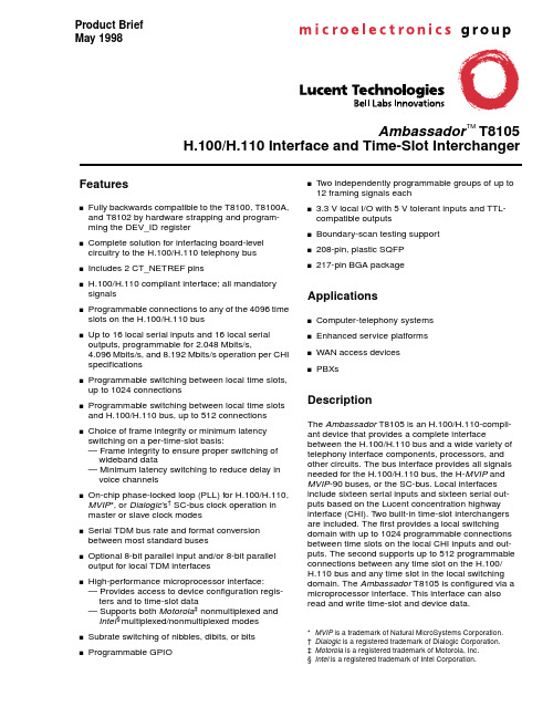
Product BriefMay 1998Ambassador TM T8105H.100/H.110 Interface and Time-Slot InterchangerFeaturess Fully backwards compatible to the T8100, T8100A, and T8102 by hardware strapping and program-ming the DEV_ID registers Complete solution for interfacing board-level circuitry to the H.100/H.110 telephony buss Includes 2 CT_NETREF pinss H.100/H.110 compliant interface; all mandatory signalss Programmable connections to any of the 4096 time slots on the H.100/H.110 buss Up to 16 local serial inputs and 16 local serial outputs, programmable for 2.048 Mbits/s,4.096 Mbits/s, and 8.192 Mbits/s operation per CHI specificationss Programmable switching between local time slots, up to 1024 connectionss Programmable switching between local time slots and H.100/H.110 bus, up to 512 connectionss Choice of frame integrity or minimum latency switching on a per-time-slot basis:— Frame integrity to ensure proper switching of wideband data— Minimum latency switching to reduce delay in voice channelss On-chip phase-locked loop (PLL) for H.100/H.110, MVIP*, or Dialogic’s† SC-bus clock operation in master or slave clock modess Serial TDM bus rate and format conversion between most standard busess Optional 8-bit parallel input and/or 8-bit parallel output for local TDM interfacess High-performance microprocessor interface:— Provides access to device configuration regis-ters and to time-slot data— Supports both Motorola‡ nonmultiplexed and Intel§ multiplexed/nonmultiplexed modess Subrate switching of nibbles, dibits, or bitss Programmable GPIO s T wo independently programmable groups of up to 12 framing signals eachs 3.3 V local I/O with 5 V tolerant inputs and TTL-compatible outputss Boundary-scan testing supports208-pin, plastic SQFPs217-pin BGA packageApplicationss Computer-telephony systemss Enhanced service platformss WAN access devicess PBXsDescriptionThe Ambassador T8105 is an H.100/H.110-compli-ant device that provides a complete interface between the H.100/H.110 bus and a wide variety of telephony interface components, processors, and other circuits. The bus interface provides all signals needed for the H.100/H.110 bus, the H-MVIP and MVIP-90 buses, or the SC-bus. Local interfaces include sixteen serial inputs and sixteen serial out-puts based on the Lucent concentration highway interface (CHI). T wo built-in time-slot interchangers are included. The first provides a local switching domain with up to 1024 programmable connections between time slots on the local CHI inputs and out-puts. The second supports up to 512 programmable connections between any time slot on the H.100/ H.110 bus and any time slot in the local switching domain. The Ambassador T8105 is configured via a microprocessor interface. This interface can also read and write time-slot and device data.*MVIP is a trademark of Natural MicroSystems Corporation.†Dialogic is a registered trademark of Dialogic Corporation.‡Motorola is a registered trademark of Motorola, Inc.§Intel is a registered trademark of Intel Corporation.2Lucent Technologies Inc.Product BriefMay 1998H.100/H.110 Interface and Time-Slot InterchangerAmbassador T8105Description (continued)Onboard clock circuitry , including a digital phase-locked loop, supports all H.100/H.110 clock modes including MVIP and SC-bus compatibility clocks. The local CHI interfaces support PCM rates of 2.048 Mbits/s,4.096 Mbits/s, and 8.192 Mbits/s. The Ambassador T8105 has internal circuitry to support either minimum latency or multi-time-slot frame integrity. Frame integrity is a requisite feature for applications that switch wideband data (ISDN H-channels). Minimum latency is advantageous in voice applications.5-6101(F)cFigure 1. Block Diagram of the Ambassador………H.100, H.110, H-MVIPINTERNAL CLOCKS ANDSTATE COUNTERS/P AND P/S CONVERTERS512LOCATION DATA SRAMTHREE 512LOCATION CONNECTIONCAMs1024LOCATION DATA MEMORY OUTPUT LOGIC AND P/S CONVERTINPUT LOGIC AND S/P CONVERT 1024LOCATION CONNECTION MEMORYTIMING AND CONTROLMICROPROCESSORINTERFACEFRAME GROUP INTERFACE LOGICFRAME GROUPSADDR[1:0]DATA[7:0]µP CONTROLSMISC. I/OCLOCKS AND REFSINTERNAL DATAINTERNAL ADDRESS AND CONTROLLOCAL OUTLOCAL INProduct BriefMay 1998H.100/H.110 Interface and Time-Slot InterchangerAmbassador T8105Application OverviewThe integration of computers and telecommunications has enabled a wide range of new communications applications and has fueled an enormous growth in communications markets. A key element in the devel-opment of computer-based communications equipment has been the addition of an auxiliary telecom bus to existing computer systems. Most manufacturers of high-capacity, computer-based telecommunications equipment have incorporated some such telecom bus in their systems. T ypically, these buses and bus inter-faces are designed to transport and switch Nx64 kbits/s low-latency telecom traffic between boards within the computer, independent of the computer’s I/O and mem-ory buses. At least a half dozen of these PC-based telecom buses emerged in the early 1990s for use within equipment based on ISA/EISA and MCA com-puters.With the advent of the H.100/H.110 bus specification by the Enterprise Computer T elephony Forum, the com-puter-telephony industry has agreed on a single tele-com bus for use with PCI and compact PCI computers.H.100/H.110 facilitates interoperation of components, thus providing maximum flexibility to equipment manu-facturers, value-added resellers, system integrators, and others building computer-based telecommunica-tions applications.Subrate switching is the ability to switch part(s) of one byte from one stream/time slot to another stream/time slot. The parts are the following:s Nibbles (4 bits)—representing a 32 kbits/s subrates Dibits (2 bits)—representing a 16 kbits/s subrates Bits—representing an 8 kbits/s subrateH.100/H.110 data transfers are always bytes. If subrate switching is used, the T8100A constructs a byte con-sisting of the subrate samples. The constructed byte may contain any combination of nibbles, dibits, or bits. In addition, individual data bits can be placed within a byte along with don’t care bits.5-6099FFigure 2. CTI Call Center Application DATABASEETHERNETCTI SERVERUSER EXTENSIONSASRFAXT1/E1ISDNPCIBUSH.100/H.110 BUSTO PSTNT1E1ISDNLucent Technologies Inc.3Lucent T echnologies Inc. reserves the right to make changes to the product(s) or information contained herein without notice. No liability is assumed as a result of their use or application. No rights under any patent accompany the sale of any such product(s) or information. Ambassador is a trademark of Lucent T echnologies Inc.Copyright © 1998 Lucent T echnologies Inc.All Rights Reserved Printed in U.S.A.May 1998PN98-141NTNBPrinted On Recycled PaperFor additional information, contact your Microelectronics Group Account Manager or the following:INTERNET:/micro E-MAIL:docmaster@ N. AMERICA:Microelectronics Group, Lucent T echnologies Inc., 555 Union Boulevard, Room 30L-15P-BA, Allentown, P A 181031-800-372-2447, FAX 610-712-4106 (In CANADA: 1-800-553-2448, FAX 610-712-4106)ASIA P ACIFIC:Microelectronics Group, Lucent T echnologies Singapore Pte. Ltd., 77 Science Park Drive, #03-18 Cintech III, Singapore 118256Tel. (65) 778 8833, FAX (65) 777 7495CHINA:Microelectronics Group, Lucent T echnologies (China) Co., Ltd., A-F2, 23/F , Zao Fong Universe Building, 1800 Zhong Shan Xi Road,Shanghai 200233 P . R. China Tel. (86) 21 6440 0468, ext. 316, FAX (86) 21 6440 0652JAP AN:Microelectronics Group, Lucent T echnologies Japan Ltd., 7-18, Higashi-Gotanda 2-chome, Shinagawa-ku, T okyo 141, JapanTel. (81) 3 5421 1600, FAX (81) 3 5421 1700EUROPE:Data Requests: MICROELECTRONICS GROUP DA T ALINE: Tel. (44) 1189 324 299, FAX (44) 1189 328 148T echnical Inquiries:GERMANY: (49) 89 95086 0 (Munich), UNITED KINGDOM: (44) 1344 865 900 (Bracknell),FRANCE: (33) 1 48 83 68 00 (Paris), SWEDEN: (46) 8 600 7070 (Stockholm), FINLAND: (358) 9 4354 2800 (Helsinki), IT AL Y: (39) 2 6608131 (Milan), SP AIN: (34) 1 807 1441 (Madrid)Product BriefMay 1998H.100/H.110 Interface and Time-Slot InterchangerAmbassador T8105T8105 Selection GuideFeaturesT8100T8100A T8102T8105Subrate switching —√√√Local-to-local connections 1,0241,024—1,024Local-to-H.100 connections256256512512CT_NETREFs1222。
超导磁体电源

M o d e l 430 P o w e r S u p p l y P r o g r a m m e r S p e c i f i c a t i o n s f o r A M I ’s S t a n d a r d S y s t e m s @ 25o CStandard Model 430 Configurations: Programmable LimitsMagnet Current Control Parameter±5 A±10 A +100 A ±125 A +200 A ±250 A +300 A +500 AAccuracy a (A) with Standard Shunt System: 0.002 0.004 0.04 0.05 0.08 0.1 n/a bn/a bAccuracy c(A) - High Stability System: 0.000250.0005 0.005 0.0063 0.01 0.0125 0.015 0.025Stability a(A) with Standard Shunt System: 0.001d0.002d0.02d0.025d0.04d0.05dn/a bn/a bStability c(A) - High Stability System: 0.000050.0001 0.001 0.001250.002 0.0025 0.003 0.005 Minimum Ramp Rate (mA/min): 0.01 0.01 0.01 0.1 0.1 0.1 0.1 0.1 Maximum Ramp Rate (A/sec):1111020203030aAfter 20 minutes; stability and accuracy of systems 250 A and less bare improved more than a factor of 10 with the optional high-stability (flux-gate) system.bSystems larger than 250 A include the high stability (flux-gate) option as the standard configuration. c After 10 minutes; d Drift is further reduced to half that shown after 60 minutes.Model 430 Power Supply ProgrammerandIntegrated Magnet Power Supply SystemsShown here: AMI’s most popular Magnet Power Supply System, the Model 4Q06125PS-430Model 430 ProgrammerIntegrated Power Supply SystemsThe AMI Model 430 Power Supply Programmer is a sophisticated digital power supply controller that allows an operator to manage a superconducting magnet system with unprecedented accuracy and ease. The Model 430 is designed to control a wide range of single, dual, and four-quadrant linear and switching power supplies. The most frequently used functions are accessible via single keystroke or shift plus keystroke. For other functions, a menu driven format guides the user to enter inputs using the push button front panel interface.AMI Integrated Magnet Power Supply Systems incorporate the digitally based Model 430 Power Supply Programmer which provides simplified, flexible operation with precise low drift magnet current control. Standard systems are mounted in rugged 19” rack-style cabinets. Standard 4-quadrant systems range from 5 A to 250 A, while the standard bipolar current ratings range from 100 A to 500 A. Bipolar systems incorporate the AMI Model 601 Energy Absorber to achieve bipolar operation and allow fast ramp down with a unipolar power supply.Multi-axis SystemsMultiple Model 430 Power Supply Programmers can control a multi-axis magnet system for virtual rotation of the magnetic field. An infinite combination of field vectors is possible when the coils of the multi-axis magnet system are energized and controlled independently and simultaneously.Model 430 Features•Parameter for setting persistent switch cool time1•Ultrahigh resolution and accuracy•Intuitive user operation and comprehensive manual2•Upper current limit and voltage limit settings•Easy to read digital V m/V s (magnet and supply voltage) display meter•Can automatically determine inductance of load•Drivers for LabView•User-adjustable threshold quench detection with detection I/O••Galvanically isolated Program Output signal to prevent ground loops•Multifunction vacuum fluorescent display (VFD)•Menu driven user interface and keypad – logical and intuitive•One touch Ramp/Pause button•Digital readout in Field (kilogauss or Tesla) or Current (Amperes)•Control multiple parallel or series configured supplies•Front panel indication that current is flowing in magnet leads•Velocity sensitive encoder dial for fine adjustments•Programmable piecewise-continuous ramping with 10 current-dependent rates•I ntegrated DB-25 magnetstation connector with wiredDB-25 output signals availablefor other system devices•Built-in Ethernet and RS-2323 communication interfaces•Ethernet port allows access to the Programmer across a local network or via the Internet•Operating software is stored in flash memory and can easily be updated via the Ethernet or RS-232 ports1Important for conduction-cooled magnets (dry switch) when a relatively long time is required to cool as compared with wet switches.2Manual is conveniently available in the Model 430 firmware (pdf format) - just access the instrument’s IP address via a web browser.3An optional external conversion unit is available for interfacing the RS-232 serial port to a GPIB bus.Simplified OperationMost frequently used functions are accessible via single keystroke or shift plus keystroke. The front panel velocity-accelerated rotary encoder dial also allows the operator to make fine adjustments to operating parameters of the magnet system. Magnet system signal wiring, such as magnet voltage/current, helium levels, and temperatures, connect to the rear panel through a single DB-25 connector. Multiple connectors on the rear panel allow the user to route the signals to the appropriate instruments at the control station; the need for complicated wiring between the cryostat and magnet control station is thus eliminated.Digital ControlThe digitally-based Model 430 incorporates very high resolution analog <> digital converters and digital signal processing (DSP) to achieve excellent stability, precise control, and superior current resolution of the programmed magnetic field. An internal microcomputer manages all computations, analog data conversion, display/keypad functions, communications I/O, and analog power supply programming signals.High Resolution and StabilityPrecision instrumentation techniques and potentiometer-free designs are employed throughout the instrument to ensure accurate signal translation for a wide range of conditions. The magnet current is sampled at a resolution of 15.6 µA (for a 125 A supply) and is front-panel programmable in 0.1 mA increments. A further order of magnitude in accuracy and stability can be achieved by choosing the optional fluxgate based current measurement system in place of the standard resistive shunt.Magnet Control and ProtectionThe Model 430 protects the magnet from runaway supply voltage/current or operator error. The quench detect function, with user-adjustable quench sensitivity, is designed to detect a magnet quench and quickly stop power from being delivered to the resistive magnet. The system can optionally incorporate an AMI Liquid Helium (LHe) Level Instrument to prevent magnet quenching due to low LHe level; automatic ramp down of the magnet (even in persistent mode) is initiated if the LHe level drops to a preset level.A system administrator can program the instrument (from the front panel or remotely) with password protected operational limits or any other parameter(s) which can thereafter not be exceeded or changed without the password. During operation of the system, if the operator inadvertently attempts to take the magnet system to an excessive magnetic field strength or excessive voltage, the Programmer will not accept the parameter and will alert the operator that the value exceed the limits.The Model 430 automatically determines and sets the proper persistent switch heater current (range: 0 to 100 mA; compliance 13.5 V). The persistent switch heater circuit is continually monitored and the user is notified of circuit problems. The Model 430 Programmer automatically controls the power supply and persistent switch heater to aid the user in safe and quick transitions in and out of persistent mode.For single quadrant operation (I+, V+) the Model 430Programmer can control various unipolar switching or linearsupplies. Shown here is the AMI Model 08150PS-430 1200 wattswitching supply combination. This system offers great value,small size, and minimum heat generation. The Model 430Programmer has also been tested on older supplies such as theHP6260B linear power supply; it can breathe new life into yoursystem by offering state of the art control capability.Bipolar operation (I+, V-/+) is obtained by adding a Model 601Energy Absorber unit to take full advantage of programmedmagnetic field profiles, and other situations requiring fast rampdown rates.AMI’s lowest-power standard bipolar power supply system, designated 05100PS-430-601, has the Model 08150PS configured at 100 A/ 10 V, and in conjunction with the Model 601, supplies 100 A at 5 V to the load. The system comes mounted in a 19” rack style cabinet. Specifications for this and other standard AMI bipolar systems are outlined below. AMI’s highest-power standard bipolar power supply system, the Model 05500PS-430-601, is pictured on the last page of this brochure. Other ratings and configurations are available.Specifications – Standard Cabinet Mounted Bipolar Power Supply Systems SystemMaximumCurrentMaximumVoltageOutputPowerMaximumInput Power aTypicalNoiseDimensions bh x w x dApproximateWeight c 05100PS-430-601: +100 A ±5 Vdc 500 VA 1500 VA 75 mV p-p 12.5" x 21.0" x 24.5" 70 lb (32 kg)05200PS-430-601: +200 A ±5 Vdc 1000 VA 3000 VA 75 mV p-p 25.0" x 23.6" x 23.6" 165 lb (75 kg) 05300PS-430-601: +300 A ±5 Vdc 1500 VA 4500 VA 75 mV p-p 30.3" x 23.6" x 23.6" 215 lb (98 kg) 05500PS-430-601: +500 A ±5 Vdc 2500 VA 7250 VA 75 mV p-p 47.2" x 21.3" x 24.5" 330 lb (150 kg)a Includes Model 430 and Model 601 bRack/cabinet dimensions; h = height; w = width; d = depth c Includes rack/cabinetFor true high-current four-quadrant operation (I+/-, V+/-) the Model430 is configured with the Model 4Q06125PS Power Supply toprovide smooth, linear sweeps through zero current with constantramp rates across the entire operating range. The magnet systemcan easily be fine tuned by making precise adjustments to the currentthrough the use of the convenient velocity sensitive encoder dial. Thissystem, designated 4Q06125PS-430, comes standard in a 19” rackstyle cabinet, and is depicted on the cover page of this brochure.For higher voltage or current, series and parallel configurations of the4Q06125PS are available (designated 4Q12125PS-430 and4Q06250PS-430). For smaller magnets, four quadrant power supplysystems (designated 4Q1005PS-430 and 4Q1010PS-430)incorporate the smaller Kepco BOP supplies and are offered forsmaller magnet requirements. Specifications for standard AMI fourquadrant systems are outlined below.Other ratings and configurations are available.Specifications – Standard Cabinet Mounted Four Quadrant Power Supply Systems SystemMaximumCurrentMaximumVoltageOutputPowerMaximumInput Power aTypicalNoiseDimensions bh x w x dApproximateWeight c 4Q06125PS-430: ±125 A ±6 Vdc 750 VA 2000 VA 120 mV p-p 12.5" x 21.0" x 24.5" 100 lb (46 kg)4Q06250PS-430: ±250 A ±6 Vdc 1500 VA3800 VA 120 mV p-p 19.5" x 21.0" x 24.5" 200 lb (91 kg)4Q12125PS-430: ±125 A ±12 Vdc 1500 VA3800 VA 240 mV p-p 19.5" x 21.0" x 24.5" 200 lb (91 kg)4Q1005PS-430: ±5 A ±10 Vdc 50 VA 700 VA 10 mV p-p 12.5" x 21.0" x 24.5" 85 lb (39 kg)4Q1010PS-430: ±10 A ±10 Vdc 100 VA 1200 VA 10 mV p-p 12.5" x 21.0" x 24.5" 85 lb (39 kg)a Includes Model 430 bRack/cabinet dimensions; h = height; w = width; d = depth c Includes rack/cabinetThe Internet Protocol Model 430IP Power Supply ProgrammerWith no front panel controls except the power On/Off switch, the Model 430IP is designed for fully functional magnet system control via the rear panel Ethernet connection using TCP/IP with a web browser.Control can be established through a locally connected computer or remotely through a network or even the Internet; the human/machine interface is a web browser depiction of the Model 430. This is especially useful for multi-axis systems where a computer is an inherent part of the system. The IP-capable firmware can also be applied to the standard Model 430 with front panel controls – in this case the computer-displayed Model 430 mirrors and controls all hardware front panel devices with theexception of the ac input power switch. The following is a screen-shot of the Model 430IP being controlled with a web browser.Selecting an AMI Power Supply SystemModel 05500PS-430-601 SystemBipolar (Magnet Voltage -5 V 1to +5 V)05500PS-430-60105300PS-430-60105200PS-430-60105100PS-430-6010 A 100 A 200 A 300 A 400 A 500 A1Available for fast discharge of magnet.Four Quadrant High Current (Magnet Voltage -6 V to +6 V)4Q06250PS-4304Q06125PS-430-300 A -200 A-100 A 0 A 100 A 200 A 300 AFour Quadrant High Current (Magnet Voltage -12 V to +12 V)4Q12125PS-430 4Q12125PS-430-200 A -100 A 0 A 100 A 200 AFour Quadrant Low Current (Magnet Voltage -10 V to +10 V)4Q1010PS-430 4Q06125PS4Q1005PS-430-10 A -5 A 0 A 5 A 10 A。
外泌体之家---笔记
外泌体之家笔记外泌体简介Exosome ,中文名外泌体,是一种能被大多数细胞分泌的微小膜泡,具有脂质双层膜结构,直径大约40-100 nm 。
尽管外泌体最初在1983 年就被发现,但人们一直认为它只是一种细胞的废弃物。
然而最近几年,人们发现这种微小膜泡中含有细胞特异的蛋白、脂质和核酸,能作为信号分子传递给其他细胞从而改变其他细胞的功能。
这些发现点燃了人们对细胞分泌膜泡的兴趣。
最近的研究发现外泌体在很多生理病理上起着重要的作用,如免疫中抗原呈递、肿瘤的生长与迁移、组织损伤的修复等。
不同细胞分泌的外泌体具有不用的组成成分和功能,可作为疾病诊断的生物标志物。
外泌体具有脂质双层膜结构,能很好的保护其包被的物质,且能靶向特定)。
细胞或组织,因此是一种很好靶向给药系统(targeted delivery system2015 年,随着精准医学概念的提出,越来越多的人开始关注如何能做到疾病的精确诊断和治疗。
外泌体作为一个新型的研究热点,由于它在体内存在的广泛性和获取的便捷性,已经成为了疾病诊断治疗的潜在有效方式,在精准医学发展上有着光明的前景。
综述虽然,已有初步研究结果解释外泌体在体内的运输途径。
4)外泌体对肿瘤免疫的影响,以及对肿瘤抗放疗、抗化疗的影响。
Cell :外泌体的研究现状与未来方向--CQ号传导的功能研究仍需要一些实质性的研究来解释。
在这篇综述中,作者以肿瘤细胞及其微 环境为背景,认为癌细胞分泌的外泌体对癌症的发生及恶化起着重要的媒介调控作用。
:as-,。
・』蓄] IMF*tj 趨勰矍:魁趣 EV ZIdT dl 価n 1 niZ pKilitatiDO Dh ml[ nDLIiLvrind'Inhidupodiu Inr —■I'cp -R d ■■ H I M X U I L M■ C 石l-rr.t&J ■■«UJ - 2 lllv IsIMF DP fCU ruiPr>>rTHlActK rwclicifeliiblrVwwnli 一合尹丫AgP 二帀 flf F£i ・[i,z 号flfUiTT'F = ji-Jllff. u- J ui' iJiiJy- ^dbidlunH'al'fairrw Vniliiv e ■ EI J圭 c lU HHI 5 J I 二心ft*____常《(■ kr\.i|yb ・n —“…y一營V”厂百炉L '弦f 盘*莎Hp .!?■ !;;" j “ Ilk Cl*: i-TR. Illi- mi Fl i —I rr : ■:r«・rF*<Kf尸9在这篇Cell 文章中,作者首先总结了目前外泌体最引人注目的功能研究: 1)外泌体携带的 蛋白促进了肿瘤进展和转移;2)外泌体的分泌、运输途径等传递信号通路;3)外泌体中的但关于,其介导的细胞间的信小RNA 具有什么作用;从物理、 生化上区分开, 比如说不同类型的外泌体存在哪些不同的生物标志物, 学功能上区分不同类型的外泌体仍存在很多难题。
PCB专业术语翻译(英语)

PCB专业术语(英语)PCBprinted circuitboard 印刷电路板,指空得线路板PCBA printed circuit boardassembly印刷电路板组件,指完成元件焊接得线路板组件PWA PrintedWire Assembly,Aperturelist Editor:光圈表编辑器。
Aperturelistwindows:光圈表窗口.Annular ring:焊环。
Array:拼版或陈列.Acid trip:蚀刻死角。
Assemby:安装.Bare Bxnel:光板,未进行插件工序得PCB板。
Bad Badsize:工作台,工作台有效尺寸.BlindBuried via:盲孔,埋孔。
Chamfer:倒角。
Circuit:线路。
Circuitlayer:线路层。
Clamshell tester:双面测试机.Coordinates Area:坐标区域.Copy—protect key:软件狗。
Coutour:轮廓。
Draw:一种圆形得光圈,但只就是用于创建线路,不用于创建焊盘。
Drill Rack:铅头表。
Drill Rack Editor:铅头表编辑器。
DrillRackwindow:铅头表窗口。
DCode:Gerber格式中用不着于表达光圈得代码。
Double—sided Biard:双面板。
Endof Block character(EOB):块结束符。
Extract Netlist:提取网络.Firdacial:对位标记.Flash:焊盘,来源于早期矢量光绘机,在矢量光绘机中,焊盘就是光通过光圈“闪出”(Fla sh)而形成得。
Gerber Data:从PCBCAD系统到PCB生产过程中最常用得数据格式.Grid:栅格。
GraphicalEditor:图形编辑器.Incremental Data:增量数据。
Land:接地层。
Layer list window:层列表窗口.Layer setup Area:层设置窗口.Multilayer Board:多层板。
英文翻译——精选推荐
英⽂翻译英⽂翻译(English translation)INTRODUCTION1.0INTRODUCTIONThe AS language reference manual is designed to assist the user whose primary responsibility includes programming and operating Kawasaki industrial robots on a daily basis. AS language is a computer control language designed specifically for use with Kawasaki robot controllers. This text provides information on creating programs, running programs, and editing programs using AS language commands. AS language is relatively easy to learn with many keywords, syntax sequences, and interface commands being intuitive.AS language provides the programmer with the ability to precisely define the task a robot is to perform .Programming the robot with a computer control language (AS) also provides the ability to integrate peripheral components into the program. Typical component interfacing with AS language programs includes: programmable logic controllers (PLCs),lasers, weld controllers, gray scale vision, and remote sensing systems.AS language programs provide outstanding performance in terms of robot trajectory control. Program location points can be stored and played back as either joint angles representing the manipulator (precision points) or geometrically defined locations in the work envelope (transformations). Transformations locations can also be defined based on their relative position to one another (compound transformations).These capabilities allow program locations to be shifted and moved based on parameters and variables and identified in the AS language program.简介1.0简介由于语⾔参考⼿册的⽬睹是帮助⽤户,其主要职责包括编程和操纵川崎⼯业机器⼈的⽇常⼯作。
自动化专业-外文文献-英文文献-外文翻译-plc方面

1、外文原文(复印件)A: Fundamentals of Single-chip MicrocomputerTh e si ng le-ch i p mi cr oc om pu ter is t he c ul mi nat i on o f bo th t h e d ev el op me nt o f th e d ig it al com p ut er an d t he int e gr at ed ci rc ui ta r gu ab ly th e t ow m os t s i gn if ic ant i nv en ti on s o f t h e 20t h c en tu ry[1].Th es e to w t ype s o f a rc hi te ct ur e a re fo un d i n s i ng le—ch ip m i cr oc om pu te r。
S o me em pl oy th e s p li t p ro gr am/d at a me mo ry of t he H a rv ar d ar ch it ect u re, sh ow n in Fi g.3-5A—1,ot he r s fo ll ow t hep h il os op hy, wi del y a da pt ed f or ge n er al—pu rp os e c o mp ut er s an dm i cr op ro ce ss or s, of ma ki ng no lo gi c al di st in ct io n be tw ee n p ro gr am a n d da ta m em or y a s i n th e Pr in cet o n ar ch it ec tu re,sh ow n in F ig。
3-5A-2.In g en er al te r ms a s in gl e—ch i p mi cr oc om pu ter isc h ar ac te ri zed b y the i nc or po ra tio n of al l t he uni t s o f a co mp ut er i n to a s in gl e de v i ce,as s ho wn i n F ig3—5A—3。
毕业设计英文翻译-智能热能表控制器外文翻译-中英文文献对照翻译

外文资料与中文翻译外文资料:Intelligent thermal energy meter controllerAbstractA microcontroller based, thermal energy meter cum controller (TEMC) suitable for solar thermal systems has been developed. It monitors solar radiation, ambient temperature,fluid flow rate, and temperature of fluid at various locations of the system and computes the energy transfer rate. It also controls the operation of the fluid-circulating pumpdepending on the temperature difference across the solar collector field. The accuracyof energy measurement is ±1.5%. The instrument has been tested in a solar water heatingsystem. Its operation became automatic with savings in electrical energy consumption ofpump by 30% on cloudy days.1 IntroductionSolar water heating systems find wide applications in industry to conserve fossil fuel like oil, coal etc. They employ motor driven pumps for circulating water with on-offcontrollers and calls for automatic operation. Reliability and performance of the system depend on the instrumentation and controls employed. Multi-channel temperature recorders, flow meters, thermal energy meters are the essential instruments for monitoring andevaluating the performance of these systems. A differential temperature controller (DTC) is required in a solar water heating system for an automatic and efficient operation ofthe system. To meet all these requirements, a microcontroller based instrument wasdeveloped. Shoji Kusui and Tetsuo Nagai [1] developed an electronic heat meter formeasuring thermal energy using thermistors as temperature sensors and turbine flow meter as flow sensor.2 Instrument detailsThe block diagram of the microcontroller (Intel 80C31) based thermal energy meter cum controller is shown in Fig. 1. RTD (PT100, 4-wire) sensors are used for the temperaturemeasurement of water at the collector field inlet, outlet and in the tank with appropriate signal conditioners designed with low-drift operational amplifiers. A precision semiconductor temperature sensor (LM335) is used for ambient temperature measurement. A pyranometer, having an output voltage of 8.33 mV/kW/m2, is used for measuring the incident solar radiation. To monitor the circulating fluid pressure, a sensor with 4–20 mA output is used. This output is converted into voltage using an I-V converter. All these outputsignals are fed to an 8-channel analog multiplexer (CD4051). Its output is fed to adual-slope 12-bit A/D converter (ICL7109). It is controlled by the microcontroller through the Programmable Peripheral Interface (PPI-82C55).Fig. 1. Block diagram of thermal energy meter cum controller.A flow sensor (turbine type) is used with a signal conditioner to measure the flowrate. Its output is fed to the counter input of the microcontroller. It is programmed tomonitor all the multiplexed signals every minute, compute the temperature difference,energy transfer rate and integrated energy. A real-time clock with MM58167 is interfacedto the microcontroller to time-stamp the logged data. An analog output (0–2 V) is provided using D/A converter (DAC-08) to plot both the measured and computed parameters. A 4×4 matrix keyboard is interfaced to the microcontroller to enter the parameters like specificheat of liquid, data log rate etc. An alphanumeric LCD display (24-character) is alsointerfaced with the microcontroller to display the measured variables. The serialcommunication port of the microcontroller is fed to the serial line driver and receiver(MAX232). It enables the instrument to interface with the computer for down-loading thelogged data. A battery-backed static memory of 56K bytes is provided to store the measured parameters. Besides data logging, the instrument serves as a DTC. This has been achievedby interfacing a relay to the PPI. The system software is developed to accept thedifferential temperature set points (ΔT on and ΔT off) from the keyboard. An algorithmsuitable for on-off control having two set-points is implemented to control the relays.3 Instrument calibrationThe amount of energy transferred (Q) is :Where = mass flows rate of liquid kg/s ; V = volumetric flow rate (l/h) ; ρ= density of water (kg/l) ; Cp = specific heat (kJ/kg°C); and ΔT = temperature difference between hot and cold (°C).The accuracy in energy measurement depends on the measurement accuracy of individual parameters. Temperature measurement accuracy depends on the initial error in the sensorand the error introduced due to temperature drifts in the signal conditioners and the A/D converter. The temperature sensor is immersed in a constant temperature bath (HAAKE B ath-K, German), whose temperature can be var ied in steps of 0.1°C. A mercury glass thermometer (ARNO A MARELL, Germany) with a resolution of 0.05°C is also placed along with PT100 sensor in the bath. This is compared with the instrument readings. The accuracy of the instrument in temperature measurem ent is ±0.1°C. Hence, the accuracy in differential temperature measurement is ±0.2°C.The flow sensor having a maximum flow rate of 1250 l/h is used for flow measurement.It is calibrated by fixing it in the upstream of a pipeline of length 8 m. The sensor output is connected to a digital frequency counter to monitor the number of pulses generated withdifferent flow rates. Water collected at the sensor outlet over a period is used forestimating the flow rate. The K-factor of the sensor is 3975 pulses/l. The uncertaintyin flow measurement is ±0.25% at 675 l/h. Uncertainties in density and specific heat ofwater are ±0.006 kg/l and ±0.011 kJ/kg°C respectively.Maximum amount of energy collection (Q) = 675×0.98×4.184×15/3600 = 11.53kW. Uncertainty in energy measurementωq/Q = [(ωv/V)2 + (ωρ/ρ)2 + (ωcp/Cp)2+(ωt/T )2]1/2.Inaccuracy in electronic circuitry is ±0.03 kW.The net inaccuracy in energy measurement is ±1.5%4 Field testThe instrument is incorporated in a solar water heating system as shown in Fig. 2.It consists of five solar flat plate collectors having an absorber area of 1.6 m2 each. The absorber is a fin and tube extruded from aluminium and painted with matt black paint. The collectors are mounted on a rigid frame facing south at an angle equal to the latitude of Bangalore (13°N). They are arranged in parallel configuration and connected to athermally insulated 500 l capacity storage tank. A 0.25 hp pump is used for circulatingthe water through the collector field. All the pipelines are thermally insulated. Thetemperature sensors and the flow sensor are incorporated in the system as shown in Fig.2. The data on solar radiation, ambient temperature, water flow rate, solar collector inlet and outlet temperatures and the system heat output are monitored at regular intervals.Fig. 2. Solar water heating system with thermal energy meter cum controller.The performance of the solar water heating system with TEMC on a partial cloudy dayis shown in Fig. 3. It is observed that DTC switched OFF the pump around 14:40 h as thereis no further energy gain by the collector field. This in turn reduced the heat lossesfrom the collector to ambient. Experiments are conducted with and without DTC o n both sunny and cloudy days. The DTC operated system shows the savings in electrical energy by 30%on a partial cloudy day and 8% on a sunny day. The variation in system output with andwithout DTC i s around 3%. Thus the controller has not only served as an energy conservation device, but also switches ON/OFF the system automatically depending on the availabilityof solar radiation. The collector field output (shown in Fig. 3) is calculated by measuring the fluid flow rate using volumetric method and the temperature difference with anotherpair of standard thermometers. It is 16.86 kWh. It is compared with the instrument reading 17.18 kWh. Thus, the deviation is 1.9%. Fig. 3 shows that the solar collector fieldefficiency is 54% when the incident solar irradiation is 31.75 kWh.Fig. 3. Performance of SWH system with TEMC on a partial cloudy day.5 Concluding remarksTEMC is used as on-line instrument in solar water heating systems for the measurement of thermal energy, temperature, flow rate with simultaneous control on the operation ofthe pump t o save electrical energy and enhance the thermal energy collection. Since several options are provided in the instrument, it can be used for monitoring the energy transfer rate in other thermal systems.AcknowledgementsThe authors are thankful to Department of Science and Technology, Govt. of India forproviding the financial assistance to carry out the above work.References1. Shoji Kusui, Tetsuo Nagai. An electronic integrating heat meter. IEEE Trans. onInstrumentation and Measurement, 1990;39(5):785-789.中文翻译:智能热能表控制器摘要适用于太阳能热系统的单片机热能表控制器(TEMC)已经研制成功。
卡洛·加茨智能组件Dupline系列产品说明说明书

Building Automation FieldbusesOverviewOverview The systemIntroductionCarlo Gavazzi’s Dupline® is a fieldbus that offers unique solutions for a wide range of applications such as mining, irrigation, elevators and energy management. The system transmits multiple digital and analog signals over several km, via an ordinary 2-wire cable. The modular design and simple operation enable it to be used easily in new or existing applications. Solutions are engineered by combining productsfrom the wide range of Dupline® modules, including digitaland analog I/O modules, PLC and PC interfaces, HMIs and modems. All modules are connect to the same 2-wire cable, which is used to exchange data between modules and between a central controller and modules.Flexible and modular remote I/O-systemDupline® is typically used as a remote I/O system, creating a link between field devices, such as sensors, contactors, valves, push buttons etc. and a central Monitoring Controller, which may be a PLC, PC or the Dupline® Controller. Dupline® can also be used as a simple wire replacement system where signals are transmitted peer-to-peer without involving a controller or other intelligent unit. The Dupline® signals can be transmitted not only on copper wire, butalso on fibre optic cable, via radio modem, on leased telephonelines or via GSM Modem. Dupline® has proven its performance inmore than 150,000 installations worldwide since 1986. And even though the latest ASIC technology is used today, the new Dupline®modules are still compatible with those installed 20 years ago.Unique set of featuresMany criteria have to be considered when selecting a fieldbus system. These include transmission distance capabilities, easy operation, noise immunity, topology, response-time and of course cost-effectiveness. Therefore, it is important to define the key application requirements in order to optimize the bus system for the specific task.The strength of the Dupline® system lies in a unique set of features that enable smart, flexible and cost-effective solutions for a wide rangeof applications. The efficiency of the protocol allows a low carrier frequency of 1 kHz, providing a long transmission distance and superior noise immunity. Hence, Dupline® is capable of transmitting multiple digital and analog signals over distances up to 10 km, viaa non-shielded, non-twisted 2-wire cable, without using repeaters.Flexible cabling and easy handlingThese unique Dupline® features provide considerable cost savings, especially where existing cables are available for use. Another important Dupline® characteristic is its easy in use in all project phases.No PC is required, since the coding of addresses and testing is carriedout by means of simple handheld devices. There is no need for special cables and terminations, and there are no cable routing restrictions. Many customers do their own installation, trouble-shooting and maintenance, thus eliminating the need for costly installation and service contracts. Dupline® is an independent and open system for interfacingwith basically any kind of controller. Serial interfaces with Modbusand dedicated PLC protocols, together with gateways for Profibus-DPand Devicenet, enable easy and flexible interfacing to PLCs, PCs and dedicated controllers.Applications and benefitsWater distributionControl and monitoring of pumps, valves, levels and flow over long distances, with or without wires.• Up to 10 km transmission distance without Repeaters • No special cable requirements: existing cable can be used • Easy handling• All signals can be controlled and monitored from any point in the system• Transmission via GSM Modem, Radio Modem or Fibre Optics possible• Flexible interfacing to PLCs,PCs and RTUs• Cost-effectiveLong conveyorsSafe monitoring of pull-wire emergency stop switches with DuplineSafe precise diagnostic information.• Immediate and precise diagnostics• Safer than traditional emergency stop systems• Approved by TÜV according to EN/I EC61508-SI L3 and EN954-1 Cat.4• Up to 5 km transmission distance without repeater• High noise immunity – false trips avoided• Easy to design, install and commission a system• Several safety relays can read the same input modules Elevators3-wire bus solution for power and transmission of signals from push-buttons, lamps and floor indicators.• Provides significant reduction in installation and commisioning time• Simple to handle and easy to apply• Industrial grade and noise immune• Cost-effectiveIrrigationControl and powering of multiple values, monitoring of flow, valve position and water consumption.• Reduced installation time• Reduced cable cost• Easy to expand or change an installation• Extremely user-friendly• Free topology• Robust, reliable and proven technology• Flexible interfacing to irrigation controllers• Cost-effectiveOverviewFieldbuses - IndustrialG38000016230• Programmable channel generator• Supports various protocols for PLC such as Modbus RTU, Allan Bradley, Mitsubishi, Omron, Schneider and Matsushita • Automatic data exchange between multiple networked Master Generators, allowing systems with up to 4096 I/O points• Real-time, timer and logic functions• Alarm monitoring • RS232 and 485 ports• Possibility of 3’rd wire operation with DC-power on the 3’rd wireControllersG34900000230• Generates 8, 16, 24, 32, 40, 48, 56, 64, 96 or 128 channels• Number of channels selectable by rotary switch • Number of sequences (1 or 2) selectable • cULus approved• Quartz-controlled oscillator • Cable compensation• LED-indication for supply and Dupline ® carrier• AC or DC power supplyChannelgeneratorG38910020230• Built-in Dupline ® channel generator• Gateways for Profibus-DP, Devicenet, Modbus RTU, Modbus/TCP• Split-I/O mode selectable • AC and DC power supply • DIN-rail mountingGatewaysD38920000230• Repeaters make anytransmission-distance possible (cascading of repeaters)• Power-booster for applications with several Dupline ®-supplied units• Minimized delay (max. 1 Dupline ® scan)• Number of channels adjusted automatically • H8-housing• LED-indication for power supply, primary Dupline ® OK and secondary Dupline ® (follows Dupline ® carrier)• Built-in channel generator function for secondary Dupline ®RepeatersG34920000230• Converts Dupline ® for transmission on optical fibre • Runs on optical multimode fibre pairs(50/125, 62.5/125)• ST type connector • Up to 5 km opticaltransmission distance with 62.5/125 fibre • DIN-rail mounting• LED-indications for supply and fibre connectionConvertersG34910040230• Long distance connection of two Dupline ® networks • Approved according to EU standard TBR 15• Watchdog output• LED-indications for Supply, Dupline ® and FailPrivate linemodemG34296470230• 4 isolated analog inputs• Inputs individually configurable for 0-20 mA, 4-20 mA or 0-10 VDC• Selectable resolution: 1/1999 or 1/255 of full scale• Selectable data format: 8-bit, Analink or 3 ½ digit BCD • Address-selection through rotary-switches• LED-indication for supply and Dupline ® carrier• LED-indication for invalid switch setting and 4-20 mA underflowAnalogue inputmodules DIN-rail G34396470230• 4 analog outputs • Outputs individually configurable for 0-20 mA, 4-20 mA or 0-10 VDC• Selectable resolution: 1/1999 or 1/255 of full scale• Selectable data format : 8-bit, AnaLink or 3 ½ digit BCD • Address-selection through rotary switches• LED-indication for supply and Dupline ® carrier• LED-indication for invalid switch setting and faulty received data• Watchdog output for faulty received dataAnalogue outputmodules DIN-rail G8810 6265• 0-10 VDC analog inputs • Analink protocol (8-bit resolution)• Uses one Dupline ® address per used input• DC-powered (15-30 VDC)• Small dimension housing for decentralizedinstallation inside wall-box or environmental sensor housings• Address programming via GAP1605Analogue inputmodules de-centralG3*******• Monostable transmitter • Optoisolated contact or NPN or PNP transistor inputs • Dupline ® powered• LED-indications for supply, input activated and Dupline ® carrier• Channel coding by GAP 1605Digital inputmodules DIN-railFieldbuses - IndustrialG34304443230• 1-, 2- or 4-channel receiver • Galvanically separated SPDT or SPST relay outputs • Load:1 x 10 A/250 VAC2 x 10 A/250 VAC 4 x 5 A/250 VAC• LED-indications for supply, outputs and Dupline ® carrier • Channel coding by GAP 1605Digital outputmodules DIN-railG8810 2201• Compact monostable transmitter• Contact inputs for pushbuttons• Input pulse prolongation • Compact housing • Dupline ® supplied• Address coding by GAP 1605• cULus approvedDigital inputmodules de-centralG8830 1143• Small sized single relay output• Load: 13 A/250 VAC • Withstands 130A inrush current• Powered via Dupline ®• Address coding by GAP 1605Digital ouputmodules de-centralG8910 1101• Inductive or Magnetic Proximity Switch • ABS housing cylindrical • Ø11, M14 or M18 housing • Supplied by Dupline ®• IP67• 1.5 m cable• Channel coding by GAP 1605 with ADAPT 1605DigitalsensorsG8911 1010• AnaLink temperature transmitter with built-in Pt 1000 sensor• Temperature range: -30°C to +60°C (-22° to +140°F)• Uses only 1 channel• Channel coding by GAP 1605• M12 connection • Easily mountable • Supplied by Dupline ®AnaloguesensorsG54606606230• 16 channel status LED indicator• Label slide for LED descriptions• Individual address coding of LED’s• Normal or inverted LED operation per 8 channel group• AC/DC power supply• NPN transistor output for loss of Dupline carrier• Horizontal panel mounting, 96 x 96 mm• Channel coding by GAP 1605Displaymodules GAP1605• Portable programming unit • Individual coding of every input or output• Group coding of an entire module• Reading of codes• Editing of channel codes • On/off-line coding ofDupline ® modules type G ....• LED display 4 x 8 LEDs • Battery powered• Easy-to-handle plug-type connectionCodingunit GTU8• Portable test unit • Monitoring of Dupline ® channel status • LCD-display• 12-key tactile keyboard • Supplied by Dupline ®• Transmission latch • Dual-group reading • Analog BCD reading • Split I/O channel readingTestunit DT01• Removes distortion caused by reflections on the Dupline ® or High-Dupline ® bus • H1-housing• For mounting on DIN-rail (EN 50022)• No power supply neededTerminationunitFieldbuses - Elevator and IrrigationG2120• Open PCB 72.3 x 59 mm • Snap locks or DIN-rail (vertical or horizontal)• 3-wire operation with DC-power on wire 3• Power supply 10-30 VDC • Operating temperature: -20°C to +50°C • Channels : 8• 8 contact inputs for push buttons or transistors • LED indications for supply and carrierInputmoduleG2130• Open PCB 74 x 59 mm • Snap locks or DIN-rail (vertical or horizontal)• 3-wire operation with DC-power on wire 3• Power supply 10-30 VDC • Operating temperature: -20°C to +50°C • Channels: 8• 8 outputs for control of floor indicators and lamps • LED indications for supply and carrierOutputmoduleG2*******• Open PCB 54 x 40 mm • Snap locks or DIN-rail (vertical or horizontal)• 3-wire operation with DC-power on wire 3• Power supply 10-30 VDC • Operating temperature: -20°C to +50°C • Channels: 4• 2 push button inputs • 2 PNP-transistor outputs • LED indications for supply and carrierInput /outputmoduleG214055.0• Open PCB 74 x 59 mm • Snap locks or DIN-rail (vertical or horizontal)• 3-wire operation with DC-power on wire 3• Power supply 10-30 VDC • Operating temperature: -20°C to +50°C • Channels: 8• 4 push-button inputs • 4 transistor outputs • LED indications for supply and carrierInput /outputmoduleG2196• Open PCB 86 x 54 mm • Snap locks or DIN-rail (vertical or horizontal)• 3-wire operation with DC-power on wire 3• Power supply 20-30 VDC • Operating temperature: -20°C to +60°C• Channels: 128 inputs and 128 outputs • 128 signals• RS 485/RS 232 interface to control system• LED indications for supply, carrier and RS485TxMastermoduleG3496• Dimensions: 77 x 72 x 70 mm • DIN-Rail, H4• Possibility for 3-wire operation with DC-power on 3 wires • Power supply 20-30 VDC • Operating temperature: 0°C to +50°C• Storage temperature: -50°C to +85°C• Channels: selectable• Plug & Play RS232/RS485• Interface with built-in protocols for specific PLC brands and Modbus• Protection degree IP20• Built-in protocol for specific PLC brands for easy interfacingMastermodule GH3440 4412• Dimensions: 77 x 72 x 70 mm • DIN-Rail, H4• I/O module for irrigation valve control• Powered through Hi-Line signal (see GH34850000)• Operating temperature: 0°C to +50°C• Storage temperature: -50°C to +85°C • Channels: 4• 2 outputs for control of 3-wire 12 VDC latching valve • 2 contact inputs • Protection degree IP20Digital I/Omodule GH6440 4412• Dimensions: 80 x 77 x 50 mm • Fully molded housing for under ground installation• I/O module for irrigation valve control• Powered through Hi-Line signal (see GH34850000)• Operating temperature: 0°C to +50°C• Storage temperature: -50°C to +85°C • Channels: 4• 2 outputs for control of 3-wire 12 VDC latching valve • 2 contact inputs • Protection degree IP67Digital I/Omodule GH3485 0000• Dimensions: 77 x 72 x 70 mm • DIN-Rail, H4• Dupline ® to Hi-Line converter • Power supply 20-30 VDC • Operating temperature: 0°C to +50°C• Storage temperature: -50°C to +85°C• Channels: Automatic adjustment •Converts the Dupline ® signal to Hi-Line 28 VDC level for control of irrigation valves (see GH3440 4412 and GH6440 4412)•Protection degree IP20Convertermodule GHTU8• Dimensions: 145 x 90 x 28 mm • Handheld• Monitoring and control of Dupline ® channels. Used for Hi-line modules• Powered through the Dupline ® network• Operating temperature: 0°C to +50°C• Storage temperature: -20°C to +85°C• Channels: Automatic adjustment • Digital, multiplexed BCD and 8-bit analogue signals• Options for latching digital signals and for reading multiplexed BCD values• Protection degree IP40TestunitDuplineSafeGS3492 / GS3493• Dimensions: 77 x 72 x 70 mm• Runs on optical multimode fibre pairs (50/125, 62.5/125)• ST type connector• For mounting on DIN-rail (EN50022)• AC power supply• Up to 5 km / 3.1 miles optical transmission distance with 62.5/125 fibre• Converts DuplineSafe for transmissionon optical fibreOpticalconverters GSTI50• Dimensions: 55 x 70 x 15 mm• Enables monitoring of safety signals from text displays, touchscreens, PLCs and PCs• Power supply from bus and text display • Approvals/Marks: cULus approved • Small dimension housing for mounting directly at text display• Several GSTI50s can be connected tothe same busModbus RS485 gateway GS3891• Dimensions: 77 x 144 x 70 mm • Profibus-DP slave according to EN50170 • For mounting on DIN-rail (EN50022)• 230 VAC power supply • Approvals/Marks: cULus approved• Makes DuplineSafe diagnostics available on Profibus-DP• Several gateways can be connected to the same bus•Useful for interfacing to PLCs and PCs Profibus DP gatewayGS7510• Dimensions: 36 x 57.5 x 16.4 mm • Powered by the bus • IP67 rating• Approvals/Marks: cULus approved• Approved by TÜV Rheinland Group according to EC/EN 61508-SIL3, IEC/EN 62061-SIL3 and ISO/EN 13849-1 PL e• Easy coding and testing with handheld programming tool•Small dimensions (57.5 x 36.0 x 16.4 mm) for decentralized installation at theactual location of the safety switchInput modulesGS7380• Dimensions: 145 x 90 x 28 mm• Used for address coding of GS75102101 and configuration of GS38300143230• Battery-powered• Can be connected at any point on the bus to read out status of all safety signals •Easy-to-useHandheld programmingand test toolGS3830• Dimensions: 77 x 144 x 70 mm • Monitors up to 63 safety input modules • For mounting on DIN-rail (EN50022)• 230 VAC power supply• Approvals/Marks: cULus approved•Approved by TÜV Rheinland Group according to IEC/EN 61508-SIL3, IEC/EN 62061-SIL3 and ISO/EN 13849-1 PL e • Automatic or manual restart• Status output for external equipment • Easy configuration and testing with handheld programming toolSafety relayoutput moduleGS3391• Dimensions: 90 x 35 x 58.5 mm• 24 VDC power supply• For mounting on DIN-Rail• Profinet-DP slave•Makes DuplineSafe diagnosticsavailable on Profinet-DP• Up to 7 master generators can be connected via the HS RS485 bus (side connector)• Built-in mini-webserver • Interfacing with PLCs and PCsDupline ® profinetgateway GS3390• Dimensions: 90 x 35 x 58.5 mm • 24 VDC power supply • For mounting on DIN-Rail• Module that generates 128 Dupline ® channels and power to the bus modules • Extended digital output mode for Profinet•Generates Dupline ® carrier signal• Supports digital I/O, Analink I/O, Mux BCD I/O, 8-digit I/ODupline ® masterchannel generatorF I E L D B U S E S O V E R V I E W E NG 05/2018S p e c i fi c a t i o n s a r e s u b j e c t t o c h a n g e w i t h o u t n o t i c e . I l l u s t r a t i o n s a r e f o r e x a m p l e o n l y .Printed on 100% recycled paperproduced usingpost consumer de-inked waste.Carlo Gavazzi Automation SpA Via Milano, 13I-20020 - Lainate (MI) - ITALY Tel: +39 02 931 761**************************DENMARKCarlo Gavazzi Industri A/S HadstenCHINACarlo Gavazzi Automation (Kunshan) Co., Ltd.KunshanITALYCarlo Gavazzi Controls SpA BellunoMALTACarlo Gavazzi Ltd ZejtunLITHUANIAUab Carlo Gavazzi Industri Kaunas KaunasAUSTRIACarlo Gavazzi GmbH Ketzergasse 374,A-1230 WienTel: +43 1 888 4112Fax: +43 1 889 10 53**********************BELGIUMCarlo Gavazzi NV/SA Mechelsesteenweg 311,B-1800 VilvoordeTel: +32 2 257 4120Fax: +32 2 257 41 25*********************DENMARKCarlo Gavazzi Handel A/S Over Hadstenvej 40,DK-8370 HadstenTel: +45 89 60 6100Fax: +45 86 98 15 30*****************FINLANDCarlo Gavazzi OY AB Ahventie, 4 B FI-02170 EspooTel: +358 9 756 2000*****************ITALYCarlo Gavazzi SpA Via Milano 13,I-20020 LainateTel: +39 02 931 761Fax: +39 02 931 763 01*******************NETHERLANDS Carlo Gavazzi BV Wijkermeerweg 23,NL-1948 NT Beverwijk Tel: +31 251 22 9345Fax: +31 251 22 60 55********************NORWAYCarlo Gavazzi AS Melkeveien 13,N-3919 Porsgrunn Tel: +47 35 93 0800Fax: +47 35 93 08 01***************PORTUGALCarlo Gavazzi LdaRua dos Jerónimos 38-B,P-1400-212 LisboaTel: +351 21 361 7060Fax: +351 21 362 13 73****************************FRANCECarlo Gavazzi SarlZac de Paris Nord II, 69, rue de la Belle Etoile,F-95956 Roissy CDG Cedex Tel: +33 1 49 38 98 60Fax: +33 1 48 63 27 43***************************GERMANYCarlo Gavazzi GmbH Pfnorstr. 10-14D-64293 Darmstadt Tel: +49 6151 81000Fax: +49 6151 81 00 40***************GREAT BRITAINCarlo Gavazzi UK Ltd 4.4 Frimley Business Park,Frimley, Camberley, Surrey GU16 7SG Tel: +44 1 276 854 110Fax: +44 1 276 682 140*********************.ukSPAINCarlo Gavazzi SAAvda. Iparraguirre, 80-82,E-48940 Leioa (Bizkaia)Tel: +34 94 480 4037Fax: +34 94 431 6081******************SWEDENCarlo Gavazzi AB V:a Kyrkogatan 1,S-652 24 Karlstad Tel: +46 54 85 1125Fax: +46 54 85 11 77********************SWITZERLAND Carlo Gavazzi AGVerkauf Schweiz/Vente Suisse Sumpfstrasse 3,CH-6312 Steinhausen Tel: +41 41 747 4535Fax: +41 41 740 45 40********************USACarlo Gavazzi Inc.750 Hastings Lane,Buffalo Grove, IL 60089, USA Tel: +1 847 465 6100Fax: +1 847 465 7373**********************MEXICOCarlo Gavazzi Mexico S.A. de C.V.Calle La Montaña no. 28, Fracc. Los Pastores Naucalpan de Juárez, EDOMEX CP 53340Tel & Fax: +52.55.5373.7042****************************CANADACarlo Gavazzi Inc.2660 Meadowvale Boulevard,Mississauga, ON L5N 6M6, Canada Tel: +1 905 542 0979Fax: +1 905 542 22 48************************BRAZILCarlo Gavazzi Automação Ltda. Av. Francisco Matarazzo, 1752Conj 2108 - Barra Funda - São Paulo/SP Tel: +55 11 3052 0832Fax: +55 11 3057 1753*********************.brSINGAPORECarlo Gavazzi Automation Singapore Pte. Ltd.61 Tai Seng Avenue #05-06Print Media Hub @ Paya Lebar iPark Singapore 534167Tel: +65 67 466 990Fax: +65 67 461 980*********************.sgCHINACarlo Gavazzi Automation (China) Co. Ltd.Unit 2308, 23/F .,News Building, Block 1,1002Middle Shennan Zhong Road,Shenzhen, ChinaTel: +86 755 83699500Fax: +86 755 83699300*********************MALAYSIACarlo Gavazzi Automation (M) SDN. BHD.D12-06-G, Block D12,Pusat Perdagangan Dana 1,Jalan PJU 1A/46, 47301 Petaling Jaya,Selangor, Malaysia.Tel: +60 3 7842 7299Fax: +60 3 7842 7399**********************HONG KONGCarlo Gavazzi Automation Hong Kong Ltd.Unit 3 12/F Crown Industrial Bldg.,106 How Ming St., Kwun Tong,Kowloon, Hong Kong Tel: +852 ********Fax: +852 ********。
OMEGA用户手册 (5)

Step 30. Select the Deviation Control Type Submenu Press d . If flashing _DEV Deviation is displayed press a ,otherwise press b until flashing _DEV is shown. Now press d to store and go to next menu item.Step 31. Select the Latched Type SubmenuPress d . If flashing UNLT Unlatched is displayed press a ,otherwise press b until UNLT is displayed.Press d to store and advance to next menu item.Step 32. Select the Normally Open Type of Contact Closure SubmenuPress d . If flashing N.o.Normally Open is displayed,press a , otherwise press b until N.o.is displayed. Press d to store and advance to next menu item.Step 33. Select the Above Type of Active Submenu Press d . If flashing ABoV Above is displayed, press a ,otherwise press b until ABoV is displayed. Press d to store and advance to next menu item.Step 34. Enable Alarm 1 at Power On (A.P.oN )Press d . If flashing ENBL is displayed, press a , otherwise press b until ENBL is displayed. Press d to store and advance to next menu item.Step 35. Enter Alarm 1 High SubmenuPress a twice to skip ALR.L Alarm 1 Low value. ALR.L is for below & ALR.H for above.Step 36. Set the Alarm 1 High value (ALR.H )Press d . Press b or c until value to set the display to 002.0. Press d to save.Step 37. Enter the Alarm 2 MenuThe display will show ALR2the top menu for Alarm 2.Repeat steps from 28 to 36 to set for Alarm 2 the same conditions as for Alarm 1.Step 38. Skip the Loop Break Time Menu (LOOP )Press a to go to the OUT1Output 1 Menu item.Step 39. Configuration the Output 1 MenuSet Alarm 1 Disabled (Step 29) to be able to Enable Output 1.Configure Out 1 as CTRL / PID , ACTN / RVRS , AUTO /DSBL , ANTL / ENBL , PRoP / 000.5, REST / 0180, RATE /018.0, CYCL / 0010and DPNG / 0003. Please refer to the operator’s manual if needed. Press d to save and go to the next menu item.Step 40. Configuration of Display Color Selection Press a until the COLR Display Color Selection Menu appears on the Display. Configure COLR as N.CLR / GRN (green), 1.CLR / RED (red), 2.CLR / AMBR (amber). Please refer to the operator’s manual if needed.Step 41. Run a TestPress a until reset the controller and return to RUN Mode to display 075.0(Ambient Temperature). Now you are ready to observe temperature as it rises 10°F higher thandisplayed. Touch the tip of the Thermocouple to raise the temperature above the Alarm 2 High value 082.0, and AL2will turn on, and Display Color will change from Green to Amber. Continue touching the tip to raise the temperature above the Alarm 1 High value 087.0and Display Color will change from Amber to Red. Annunciator “1” is turning on and off displaying output 1.Step 11. Enter to the Thermocouple Type Input Submenu Press d to display flashing, previously selected Thermocouple type.Step 12. Scroll through available selection of TC types Press b to sequence thru flashing Thermocouple types,(select k -for type "K" CHROMEGA ®/ALOMEGA ®)J K T E N DIN J R S B C - TC types J k t E N dN J R S b C - DisplayStep 13. Store TC typeAfter you have selected the Thermocouple type press d to store your selection, the instrument automatically advances to the next menu item.Step 14. Enter to Reading Configuration MenuThe display shows RDG Reading Configuration, which is the top menu for 4 submenus: Decimal Point, Degree Units,Filter Constant and Input/Reading Submenus.Step 15. Enter to Decimal Point submenu Press d to show DEC Decimal Point.Step 16. Display the Decimal Point positionPress d again to display the flashing Decimal Point position.Step 17. Select the Decimal Point position Press b to select FFF.F Decimal Point position.Step 18. Store selected Decimal Point positionBy pressing d momentarily the Decimal Point position will be stored and the instrument will go to the next menu item.Step 19. Enter to Temperature Unit Submenu Display shows TEMP Temperature Unit.Step 20. Display available Temperature Units Press d to display the flashing Degree °F or °C .Step 21. Scroll through Temperature Units selection Press b to select °F Degree.Step 22. Store the Temperature UnitPress d to display momentarily that the Degree Unit has been stored and the instrument will go automatically to the next menu item.Step 23. Enter the Filter Constant Submenu Display shows FLTR Filter Constant Submenu.Step 24. Display the Filter Constant value Submenu Press d to display the flashing, previously selected Filter Constant.Step 25. Scroll through available Filter Constants Press b to sequence thru Filter Constants 0001, 0002,0004, 0008, 0016, 0032, 0064and 0128.Step 26. Store the Filter ConstantPress d momentarily to store 0004Filter Constant and the instrument will automatically go to the next menu item.Step 27. Enter Alarm 1 MenuThe display will show ALR1the top menu for Alarm 1. In the following steps we are going to enable Alarm 1, Deviation,Unlatch, Normally Open, Active Above, Enable at power on and +2°F High Alarm i.e. Process Value > Setpoint 1 Value +2°F will activate Alarm 1.If Analog Output Option is installed and enabled, the controller will skip Alarm 1 Menu item to Analog Output.Step 28. Enter Alarm 1 Enable/Disable Submenu Press d to display flashing DSBL / ENBL .Step 29. Enable Alarm 1 SubmenuIf flashing ENBL is displayed, press a , if DSBL is displayed,press b until ENBL is displayed, then press d to store and go to the next menu item.MQS3353/1204SPECIFICATIONAccuracy:+0.5°C temp;0.03% rdg. process typical Resolution:1°/0.1°; 10 µV process Temperature Stability:0.04°C/°C RTD;0.05°C/°C TC @ 25°C (77°F); 50 ppm/°C process Display:4-digits, 9-segments LED,10.2 mm (0.40") with red, green and amber programmable colors Input Types:Thermocouple, RTD, Analog Voltage and Current TC: (ITS 90)J, K, T, E, R, S, B, C, N, L RTD: (ITS 68)100/500/1000 ohm Pt sensor2-, 3-, or 4-wire; 0.00385 or 0.00392curve Voltage:0 to 100 mV, 0 to 1 V, 0 to 10 Vdc Current:0 to 20 mA (4 to 20 mA)Output 1:Relay 250 Vac @ 3 A Resistive Load,SSR, Pulse, Analog Voltage and Current Output 2:Relay 250 Vac @ 3 A Resistive Load,SSR, PulseOptions:Communication RS-232 / RS-485 orExcitation:24 Vdc @ 25 mAExc. not available for Low Power OptionLine Voltage/Power:90 - 240 Vac ±10%,50 - 400 Hz*, or 110 - 375 Vdc, 4 W* No CE compliance above 60 HzLow Voltage Power Option:12 - 36 Vdc, 3 W****Units can be powered safely with 24 Vac but No Certification for CE/UL are claimed.Dimensions:25.4 H x 48 W x 126.3 D mm (1.0 x 1.89 x 5")Weight:127 g (0.28 lb)Approvals:UL, UL-C, CE per EN61010-1:2001It is the policy of OMEGA to comply with all worldwide safety and EMC/EMI regulations that apply.OEMGA is constantly pursuing certification of its products to the European New Approach Directives.OMEGA will add the CE mark to every appropriate device upon certification.The information contained in this document is believed to be correct, but OMEGA Engineering,Inc.accepts no liability for any errors it contains, and reserves the right to alter specifications without notice.TRADEMARK NOTICE:®,®,, and are Trademarks ofOMEGA ENGINEERING, INC.®This Quick Start Reference provides informationon setting up your instrument for basic operation.The latest complete Communication and OperationalManual as well as free Software and ActiveX Controlsare available at /specs/iseries oron the CD-ROM enclosed with your shipment. SAFETY CONSIDERATIONThe instrument is a panel mount device protected in accordance with EN61010-1:2001. Remember that the unit has no power-on switch. Building installation should include a switch or circuit-breaker that must be compliant to IEC 947-1 and 947-3.SAFETY:•Do not exceed voltage rating on the label located onthe top of the instrument housing.•Always disconnect power before changing signal andpower connections.•Do not use this instrument on a work bench withoutits case for safety reason.•Do not operate this instrument in flammable orexplosive atmospheres.•Do not expose this instrument to rain or moisture. EMC:•Whenever EMC is an issue, always use shielded cables.•Never run signal and power wires in the same conduit.•Use signal wire connections with twisted-pair cables.•Install Ferrite Bead(s) on signal wire close to theinstrument if EMC problems persist.Panel Mounting Instruction:ing the dimensions from the panel cutout diagramshown above, cut an opening in the panel.2.Insert the unit into the opening from the front of thepanel, so the gasket seals between the bezel and thefront of the panel.3.Slide the retainer over the rear of the case and tightenagainst the backside of the mounting panel.ST ART HERE。
系名和专业
College of Electric Power and Automation Engineering电力与自动化工程学院Electric power Engineering 电力工程系Automation Control 自动控制系Majors:Electric Engineering and its Automation电气工程及其自动化Industrial Automation工业自动化Measure and Control Technology and Instrumentation测控技术与仪器Power-driven Engineering and Management电力工程与管理Courses:Theoretical Mechanics理论力学,Material Mechanics材料力学,Engineering Fluid Mechanics工程流体力学,Fundamentals of Mechanical Design机械设计基础,Heat and Mass Transfer传热传质学,Metallic Material金属材料,Electrotechnics and Electronics Technology电工与电子技术,Pumps and Fans泵与风机,Principles of Boilers锅炉原理,Principles of Steam Turbine气轮机原理,Refrigeration Principles and Equipment制冷原理与设备College of Computer and Information Engineering计算机与信息工程学院Computer Science and on Engineering Department计算机科学与工程系Communication Engineering Department通信工程系Electron and Information Engineering Department电自与信息工程系Majors:Computer Science and Technology 计算机科学与技术Communication Engineering 通信工程Electronic Information Engineering 电子信息工程Electronic Science and Technology 电自科学与技术Low-frequency Electronic Circuits低频电子线路,C Language Programming C程序与编程技术,Computer Construction and Logic Design计算机结构与逻辑设计,Modern Digital System Design现代数字系统设计,Digital System Labs数字系统实验,Electromagnetic Field and Waves电磁场与波,Microprocessor and Interfacing微机处理原理和接口技术,Microprocessor and Programmable Interfacing Labs微机处理器与可编程接口实验, Principle of Communications and Digital Communication通信原理与数字通信,VLSI Application大规模集成电路应用,Information Communication Network信息通信网络,Image Engineering图像工程,Optical Fiber and Mobile Communications光纤通信与移动通信,Modern Electronic Technology Labs近代电子实验,Computer Basic Skills计算机基础,Programming程序设计,Computer Network计算机网络College of Management and Humanity管理与人文学院Economy Management Department 经济管理系Social Science Department 社会科学系Majors:Business Administration 工商管理Information Management and Information System 信息管理何信息系统International Trade 国际贸易Public Affairs Management 公共事业管理Courses:Operating Research运筹学,Accounting会计学, Microeconomics微观经济学, Development and Management of Human Resources人力资源开发与管理, Macroeconomics宏观经济学, Enterprise Strategy Management企业战略管理, Production and Operations Management生产与运作管理, Introduction to Civil engineering土木工程概论, Engineering Economics工程经济学, Construction Project Management工程项目管理, Cost Estimation and Control工程估价与管理College of Energy and Environmental Engineering能源与环境工程学院Power Engineering Department动力工程系Environment Engineering Department环境工程系Majors:Thermal Energy and Power Engineering 热能动力工程Mechanics Engineering and Automation 机械工程及自动化Chemistry Technology and Water Treatment 化学工业及水处理Environment Engineering 环境工程Material Chemistry 材料化学Courses:Inorganic Chemistry无机化学, Mechanical Drawing机械制图, Organic Chemistry有机化学, Analytic Chemistry分析化学, Physical Chemistry物理化学, Principle of Chemical Engineering 化学工程原理, Environmental Monitoring环境检测, Water Pollution Control Engineering水污染控制工程, Air Pollution Control Engineering空气污染控制工程, Solid Wastes Disposal Engineering固体废弃物处置工程Department of Foreign Language直属外语系Majors:Business 商务Scientific Translation 科技翻译Travel 旅游Literature 文学Courses:Comprehensive English综合英语, Extensive English英语泛读, Spoken English英语口语, Audio-Visual English英语视听, Practical English Grammar实用英语语法, English Composition 英语写作, Business English Correspondence外贸函电, Advanced English高级英语, Advanced Spoken English高级英语口语, Business English Interpretation商务英语口译, Translation Theories and Practice翻译理论与实践。
FPGA可编程逻辑器件芯片XCVU13P-L2FLGA2577E中文规格书

General DescriptionXilinx® UltraScale™ architecture comprises high-performance FPGA, MPSoC, and RFSoC families that address a vast spectrum of system requirements with a focus on lowering total power consumption through numerous innovative technological advancements.Kintex® UltraScale FPGAs: High-performance FPGAs with a focus on price/performance, using both monolithic andnext-generation stacked silicon interconnect (SSI) technology. High DSP and block RAM-to-logic ratios and next-generation transceivers, combined with low-cost packaging, enable an optimum blend of capability and cost.Kintex UltraScale+™ FPGAs: Increased performance and on-chip UltraRAM memory to reduce BOM cost. The ideal mix of high-performance peripherals and cost-effective system implementation. Kintex UltraScale+ FPGAs have numerous power options that deliver the optimal balance between the required system performance and the smallest power envelope.Virtex® UltraScale FPGAs: High-capacity, high-performance FPGAs enabled using both monolithic and next-generation SSI technology. Virtex UltraScale devices achieve the highest system capacity, bandwidth, and performance to address key market and application requirements through integration of various system-level functions.Virtex UltraScale+ FPGAs: The highest transceiver bandwidth, highest DSP count, and highest on-chip and in-package memory available in the UltraScale architecture. Virtex UltraScale+ FPGAs also provide numerous power options that deliver the optimal balance between the required system performance and the smallest power envelope.Zynq® UltraScale+ MPSoCs: Combine the Arm® v8-based Cortex®-A53 high-performance energy-efficient 64-bit application processor with the Arm Cortex-R5F real-time processor and the UltraScale architecture to create the industry's first programmable MPSoCs. Provide unprecedented power savings, heterogeneous processing, and programmable acceleration. Zynq® UltraScale+ RFSoCs: Combine RF data converter subsystem and forward error correction with industry-leading programmable logic and heterogeneous processing capability. Integrated RF-ADCs, RF-DACs, and soft-decision FECs (SD-FEC) provide the key subsystems for multiband, multi-mode cellular radios and cable infrastructure.Family ComparisonsDS890 (v3.13) July 21, 2020Product Specification Table 1:Device ResourcesKintex UltraScale FPGAKintexUltraScale+FPGAVirtexUltraScaleFPGAVirtexUltraScale+FPGAZynqUltraScale+MPSoCZynqUltraScale+RFSoCMPSoC Processing System✓✓RF-ADC/DAC✓SD-FEC✓System Logic Cells (K)318–1,451356–1,843783–5,541862–8,938103–1,143678–930 Block Memory (Mb)12.7–75.912.7–60.844.3–132.923.6–94.5 4.5–34.627.8–38.0 UltraRAM (Mb)0–8190–3600–3613.5–22.5 HBM DRAM (GB)0–16DSP (Slices)768–5,5201,368–3,528600–2,8801,320–12,288240–3,5283,145–4,272 DSP Performance (GMAC/s)8,1806,2874,26821,8976,2877,613 Transceivers12–6416–7636–12032–1280–728–16 Max. Transceiver Speed (Gb/s)16.332.7530.558.032.7532.75 Max. Serial Bandwidth (full duplex) (Gb/s)2,0863,2685,6168,3843,2681,048 Memory Interface Performance (Mb/s)2,4002,6662,4002,6662,6662,666I/O Pins312–832280–668338–1,456208–2,07282–668280–408RF Data Converter SubsystemZynq UltraScale+ RFSoCs contain an RF data converter subsystem consisting of multiple RF-ADCs and RF-DACs.RF-ADCsThe RF-ADCs can be configured individually for real input signals. RF-ADCs in all devices other than the XCZU43DR can also be configured as a pair for I/Q input signals. The RF-ADC tile has one PLL and a clocking instance. Decimation filters in the RF-ADCs can operate in varying decimation modes at 80% of Nyquist bandwidth with 89dB stop-band attenuation. Each RF-ADC contains a 48-bit numerically controlled oscillator (NCO) and a dedicated high-speed, high-performance, differential input buffer with on-chip calibrated 100Ω termination.RF-DACsThe RF-DACs can be configured individually for real outputs. RF-DACs in all devices other than the XCZU43DR can also be configured as a pair for I/Q output signal generation. The RF-DAC tile has one PLL and a clocking instance. Interpolation filters in the RF-DACs can operate in varying interpolation modes at 80% of Nyquist bandwidth with 89dB stop-band attenuation. Each RF-DAC contains a 48-bit NCO.Soft-Decision Forward Error Correction (SD-FEC)Some members of the Zynq UltraScale+ RFSoC family contain integrated SD-FEC blocks capable of encoding and decoding using LDPC codes and decoding using Turbo codes.LDPC Decoding/EncodingA range of quasi-cyclic codes can be configured over an AXI4-Lite interface. Code parameter memory can be shared across up to 128 codes. Codes can be selected on a block-by-block basis with the encoder able to reuse suitable decoder codes. The SD-FEC uses a normalized min-sum decoding algorithm with a normalization factor programmable from 0.0625 to 1 in increments of 0.0625. There can be between 1 and 63 iterations for each codeword. Early termination is specified for each codeword to be none, one, or both of the following:∙Parity check passes∙No change in hard information or parity bits since last operationSoft or hard outputs are specified for each codeword to include information and optional parity with 6-bit soft log-likelihood ratio (LLR) on inputs and 8-bit LLR on outputs.Clock DistributionClocks are distributed throughout UltraScale devices via buffers that drive a number of vertical and horizontal tracks. There are 24 horizontal clock routes per clock region and 24 vertical clock routes per clock region with 24 additional vertical clock routes adjacent to the MMCM and PLL. Within a clock region, clock signals are routed to the device logic (CLBs, etc.) via 16 gateable leaf clocks.Several types of clock buffers are available. The BUFGCE and BUFCE_LEAF buffers provide clock gating at the global and leaf levels, respectively. BUFGCTRL provides glitchless clock muxing and gating capability. BUFGCE_DIV has clock gating capability and can divide a clock by 1 to 8. BUFG_GT performs clock division from 1 to 8 for the transceiver clocks. In MPSoCs and RFSoCs, clocks can be transferred from the PS to the PL using dedicated buffers.Memory InterfacesMemory interface data rates continue to increase, driving the need for dedicated circuitry that enables high performance, reliable interfacing to current and next-generation memory technologies. Every UltraScale device includes dedicated physical interfaces (PHY) blocks located between the CMT and I/O columns that support implementation of high-performance PHY blocks to external memories such as DDR4, DDR3, QDRII+, and RLDRAM3. The PHY blocks in each I/O bank generate the address/control and data bus signaling protocols as well as the precision clock/data alignment required to reliably communicate with a variety of high-performance memory standards. Multiple I/O banks can be used to create wider memory interfaces.As well as external parallel memory interfaces, UltraScale architecture-based devices can communicate to external serial memories, such as Hybrid Memory Cube (HMC), via the high-speed serial transceivers. All transceivers in the UltraScale architecture support the HMC protocol, up to 15Gb/s line rates. UltraScale devices support the highest bandwidth HMC configuration of 64lanes with a single FPGA.Block RAMEvery UltraScale architecture-based device contains a number of 36Kb block RAMs, each with two completely independent ports that share only the stored data. Each block RAM can be configured as one 36Kb RAM or two independent 18Kb RAMs. Each memory access, read or write, is controlled by the clock. Connections in every block RAM column enable signals to be cascaded between vertically adjacent block RAMs, providing an easy method to create large, fast memory arrays, and FIFOs with greatly reduced power consumption.All inputs, data, address, clock enables, and write enables are registered. The input address is always clocked (unless address latching is turned off), retaining data until the next operation. An optional output data pipeline register allows higher clock rates at the cost of an extra cycle of latency. During a write operation, the data output can reflect either the previously stored data or the newly written data, or it can remain unchanged. Block RAM sites that remain unused in the user design are automatically poweredPackagingThe UltraScale devices are available in a variety of organic flip-chip and lidless flip-chip packages supporting different quantities of I/Os and transceivers. Maximum supported performance can depend on the style of package and its material. Always refer to the specific device data sheet for performance specifications by package type.In flip-chip packages, the silicon device is attached to the package substrate using a high-performance flip-chip process. Decoupling capacitors are mounted on the package substrate to optimize signal integrity under simultaneous switching of outputs (SSO) conditions.。
在细胞壁上构筑的纳米结构sio-2c2-赋予植物抗逆的作用机制

华中农业大学博士学位论文在细胞壁上构筑的纳米结构SiO<,2>赋予植物抗逆的作用机制姓名:***申请学位级别:博士专业:植物营养学指导教师:王运华;李铁津2002.11.1在细胞肇上构筑的纳米结构SiOz赋予植物抗逆的作用机制摘要si是地壳中含营极为丰富的元素,在单子叶植物体内,si的含母高于任何其他无机组分,如水稻为5%一20%,燕麦、小麦和大麦等为2%_4%,却很难用一般植物营养生理学方法证明它是植物的必需营养元素,迄今仍将它列入植物的有茄营养元素。
但是,许多研究结果都证明si对植物生K发育具有有茄作用,它能明显提高植物对非生物和生物胁迫的抗性。
芥。
借助海洋生物如硅藻和海绵的生物硅化机制,从植物体矿化纳米结构Si02的形态发生、结构和功能分析入手,运用植物营养学、植物病理学、纳米化学、生物矿化的原理和技术,重点研究了以植物细胞壁为模板构筑有机/无机二元协同纳米结构s的2,以及它mj具有的特殊结构所赋予植物抵抗各种环境胁迫的可能作用.f获得的土要结果如r:l初步阐明了檀糖体内SiOl生长是团聚基妇ggregation-based)的徽结构发育机制:通常认为晶体和微结构的生长是离子在无机表面或有机模板上粘附。
借助高分辨电镜研究水稻叶外表皮系统中的si02和细胞壁基质作用时发现在硅细胞、泡状细胞和外表皮艮细胞腔中Si02是以K=2.0.3.0¨m宽o.2-0.5岬的微杆(microrods)状结构团聚而成。
微杆状结构最小微粒单元是直径为1-2m的siQ纳米球。
因此,Si02微结构的生长可以认为是大单元,微杆的组装过程,此过稗类似于从宦径儿个纳米的粒子纽装形成直径为儿目个纳米的粒子过程。
2借助SEM和TEM观察到水稻叶外表皮哑铃形硅质体的发育过程是细胞壁模板诱导的过程:在水稻叶外表皮细胞中,哑铃形袢细胞的形成是与叶片的成熟过程有芙。
在砖细胞早期的发育过程中,外表皮短细胞(shortcell)分化形成木栓.硅细胞对(cork.silicacellpairs)之后,硅细胞鼙已经构建完成,从而作为哑铃形硅质体形成的模板。
自动化课程英文描述

自动化课程英文描述Automation Course DescriptionIntroduction:The Automation Course is designed to provide students with a comprehensive understanding of automation technologies and their applications in various industries. This course aims to equip students with the necessary knowledge and skills to design, develop, and implement automated systems.Course Objectives:1. Understand the fundamentals of automation: Students will learn about the basic principles and concepts of automation, including control systems, sensors, actuators, and feedback mechanisms.2. Explore different automation technologies: Students will be introduced to a wide range of automation technologies, such as programmable logic controllers (PLCs), human-machine interfaces (HMIs), robotics, and industrial networks.3. Learn programming languages for automation: Students will gain proficiency in programming languages commonly used in automation, such as ladder logic, structured text, and function block diagram.4. Develop skills in system integration: Students will learn how to integrate various components of an automated system, including sensors, actuators, controllers, and communication networks.5. Understand safety considerations in automation: Students will be educated on safety protocols and standards in automation to ensure the safe operation of automated systems.6. Gain hands-on experience: The course will provide students with opportunities to apply their knowledge and skills through practical exercises and projects, allowing them to design, simulate, and implement automated systems.Course Outline:1. Introduction to Automation- Definition and significance of automation- Evolution of automation technologies- Applications of automation in different industries2. Control Systems- Open-loop and closed-loop control systems- Feedback and feedforward control- PID control algorithms3. Sensors and Actuators- Types and principles of sensors- Actuators and their applications- Signal conditioning and interfacing4. Programmable Logic Controllers (PLCs)- Architecture and components of PLCs- Programming languages for PLCs (ladder logic, structured text, function block diagram)- PLC programming techniques and best practices5. Human-Machine Interfaces (HMIs)- HMI design principles- HMI programming and configuration- Data visualization and user interaction6. Robotics- Introduction to industrial robots- Robot kinematics and dynamics- Robot programming and control7. Industrial Networks- Communication protocols in automation (Ethernet/IP, Modbus, Profibus) - Network topologies and architectures- Troubleshooting and maintenance of industrial networks8. System Integration- Integration of sensors, actuators, controllers, and networks- Data acquisition and processing- Real-time control and synchronization9. Safety in Automation- Risk assessment and hazard analysis- Safety standards and regulations- Emergency stop systems and safety interlocks10. Practical Projects- Design and implementation of automated systems- Simulation and testing of automated processes- Troubleshooting and optimization of automated systemsAssessment Methods:- Written examinations to evaluate theoretical knowledge- Practical assignments and projects to assess practical skills- Group discussions and presentations to encourage collaboration and communication skillsConclusion:The Automation Course provides students with a comprehensive understanding of automation technologies and their applications. By the end of this course, students will be equipped with the necessary knowledge and skills to design, develop, and implement automated systems in various industries. This course aims to prepare students for careers in automation engineering, control systems, robotics, and other related fields.。
Cypress
Cypress. EZ-USB FX2 Technical Reference ManualThe Universal Serial Bus(USB)has gained wide acceptance as the connection method of choice for low and medium speed PC peripherals. Equally successful in Windows and Macintosh worlds, USB delivered on its promises of easy attachment, an end to configuration hassles, and true plug-and-play operation.The second generation of the USB specification,”USB2.0”, extends the original specification to include:●480 Mbits/sec signaling rate, a 40x improvement over theUSB 1.1 rate of 12 Mbits/sec.●Full backward and forward compatibility with USB 1.1devices and cables.●A new hub architecture that can provide multiple 12Mbits/sec downstream ports for USB 1.1 devices.The Cypress Semiconductor EZ-USB FX2 is a single chip USB 2.0 peripheral whose architecture is similar to that of the Cypress Semiconductor EZ-USB FX family. Although much of the FX architecture is preserved, certain elements have been redesigned to accommodate the higher data rates offered by USB 2.0.Host Is MasterThis is a fundamental USB concept. There is exactly one master in a USB system: the host computer. USB devices respond to host requests. USB devices cannot send information among themselves, as they could if USB were a peer-to-peer topology.However, there is one case where a USB device can initiate signaling without prompting from the host. After being put into a low-power ”suspend” mode by the host, a device can signal a “remote wakeup”. This is the only case in which the USB device is the initiator, in all other cases, the host makes device requests and the device responds to them.There’s an excellent reason for this host-centric model. The USB architects were keenly mindful of cost, and the best way to make low-cost peripherals is to put most of the “smarts”into the host side, the PC . If USB had defined as peer-to-peer, every USB device would have required more intelligence, raising cost.1.5USB DirectionBecause the host is always the bus master, it’s easy to remember USB direction:OUT means from the host to the device, and IN means from the device to the host. FX2nomenclature uses this naming convention. For example, an endpoint that sends data to the host is an IN endpoint. This can be confusing at first, because the FX2 sends data to the host by loading an IN endpoint buffer. Likewise, the FX2 receives host data from an OUT endpoint buffer.1.7USB FramesThe USB host provides a time base to all USB devices by transmitting an SOF(start of frame)packet every millisecond. SOF packets include an 11-bit number which increments once per frame; the current frame number(0-2047)may be read from internal FX2 registers at any time.AT high speed (480 M/s),each one-millisecond frame is divided into eight 125-microsecond microframes, each of which is preceded by an SOF packet. The frame number still increments only once per millisecond, so each of those SOF packets contains the same frame number. To keep track of the current microframe number(0-7),the FX2 provides a readable microframe counter.The FX2 can generate an interrupt request whenever it receives an SOF(once every millisecond at fullspeed,or once every 125 microsecond at high speed).This SOF interrupt can be used,for example,to serviceisochronous endpoint data.1.12 EZ-USB FX2 ArchitectureThe FX2 packs all the intelligence required by a USB peripheral interface into a compact integrated circuit. As Figure 1-7 illustrates, an integrated USB transceiver connect to the USB bus pins D+ and D-. A Serial interface Engine(SIE)decodes and encodes the serial data and performs error correction, bit stuffing, and the other signaling-level tasks required by USB. Ultimately, the SIE transfers parallel data to and from the USB interface.The FX2 SIE operates at Full Speed(12M/s)and High Speed(480M/s)rates. To accommodate the increased bandwidth of USB2.0, the FX2 endpoint FIFOs and slave FIFOs(which interface to external logic or processors)are unified to eliminate internal data transfer times.The CPU is an enhanced 8051 with fast execution time and added features. It uses internal RAM for program and data storage.The role of the CPU in typical FX2-based USB peripheral is twofold:It implements the high-level USB protocol by servicing host requests over the control endpoint. However, the data rates offered by USB2.0 are too high for the CPU to process the USB data directly. For this reason, the CPU is not usually in the high bandwidth data path between endpoint FIFOs and the external interface. Instead, the CPU simply configures the interface, then “gets out of the way” while the unified FX2 FIFOs move the data directly between the USB and the external interface.The FIFOs can be controlled by an external master, which either supplies a clock and clock enable signals to operates synchronously, or strobe signals to operate asynchronously.Alternately, the FIFOs can be controlled by an internal FX2 timing generator called the General Programmable interface(GPIF). The GPIF serves as an internal master., interfacing directly to the FIFOs and generating user-programmed control signals for the interface to external logic. Additionally, the GPIF can be made to wait for external events by sampling external signals on its RDY pins. The GPIF runs much faster than the FIFOs data to give good programmable resolution for the timing signals.It can be clocked from either the internal FX2 clock or an externally supplied clock.The FX2’s CPU is rich in features. Up to five I/O ports are available, as well as two USARTs, three counter/timer, and an extensive interrupt system. It runs at a clock rate of up to 48 MHz and uses four clocks per instruction cycle instead of the twelve required by a standard 8051.The FX2 chip family uses an enhanced SIE/USB interface which simplifies FX2 code by implementing much of the USB protocol. In fact, the FX2 can function as a full USB device even without firmware.Like all EZ-USB family chips, FX2 operates at 3.3v. This simplifies FX2 code by implementing much of the USB protocol. In fact, the FX2 can function as full USB device even without firmware.Like all EZ-USB family chips, FX2 operates at3.3v. This simplifies the design of bus-powered USB devices, since the 5V power available at the USB connector(which the USB specification allows to be as low as 4.4v)can dirve a 3.3v regulator to deliver clean, isolated power to the FX2 chip.FX2 is available in a 128-pin package which brings out the8051 address bus, data bus, and control signals to allow connection of external memory and/or memory-mapped I/O. Figure 1-8 is a block diagram for this package;1.13 FX Feature SummaryFX2 includes the following features;●On-chip 480 mbits/s transceiver, PLL and SIE-the entire USB2.0 physical layer(PHY)●Double-,triple-,and quad-buffered endpoint FIFOsaccommodate the 480Mbits/s USB 2.0 data rate●Built-in, enhanced 8051 running at up to 48MHz.●Fully featured:256 bytes of register RAM, two USARTs,three timers, two data pointers.●Fast: four clocks(83.3 nanoseconds at 48Mhz)perinstruction cycle.●SFR access to control registers(including I/O ports)thatrequire high speed.●USB-vectored interrupts for low ISR latency.●Used for USB housekeeping and control, not to move highspeed data.●Soft operation—USB firmware can be downloaded overUSB, eliminating the need for hard-coded memory.●Four interface FIFOs that can be internally or externallyclocked. The endpoint and interface FIFOs are unified to eliminate data transfer time between USB and external logic.General Programmable interface(GPIF), a microcoded state machine which serves as a timing master for glueless interface to the FX2 FIFOs.FX2 is a single-chip USB2.0 peripheral solution. Unlike designs that use an external PHY, the FX2 integrates everything on one chip, eliminating costly high pin-count packages and the need to route high-speed signals between chip.1.9.1 Full-speed/high-Speed DetectionThe USB 2.0 Specification requires that high-speed(480Mbit/sec)devices begin the enumeration process in full-speed mode; devices switch to high-speed operation only after the host and device have agreed to operate at high speed. The high-speed negotiation process occurs during USB reset.When connection to a full-speed host, the FX2 will enumerate as a full-speed device. When connection to a high-speed host, the FX2 automatically switches to high-speed mode.1.9.2 EnumerationYour computer is ON. You plug in a USB device, and the Windows TM cursor switches to an hourglass and then back to a cursor. Magically, your device is connected and its Windows TM driver is loaded! Anyone who has installed a sound card into a PC and has had to configure countless jumpers, drivers, and IO/interrupt/DMA settings knows that a USB connection is miraculous. We’re all heard about Plug and play, but USB delivers the real thing.How does all this happen automatically? Inside every USB device is a table of descriptors. This table is the sum total of the device’s requirements and capabilities. When you plug into USB, the host goes through a sign-on sequence:1.The host sends a Get Descriptor-Device request to address zero(all USB devices must respond to address zero when first attached).2.T he device responds to the request by sending ID data back to the host to identify itself.3.T he host sends a Set Address request, which assigns a unique address to the just-attached device so it may be distinguished from the other devices connected to the bus. 4.T he host sends more Get Descriptor requests, asking for additional device information. From this, it learn everythingelse about the device: number of endpoints, power requirements, required bus bandwidth, what driver to load,etc.。
中医药学与合成生物学(二):toggle switch中的阴阳相互作用机制
中医药学与合成生物学(二):toggle switch中的阴阳相互作用机制冯前进【期刊名称】《山西中医学院学报》【年(卷),期】2012(013)006【总页数】2页(P封2,75)【作者】冯前进【作者单位】【正文语种】中文传统中医药学与最新发展的合成生物学(synthetic biology)之间存在有许多奇妙的联系,这是一个生动、有趣且引人入胜的话题。
关于中医药学与合成生物学的研究,前文以合成“抑制振动子(repressilator)”为例,讨论了“抑制振动子及其作用与“方-证对应相关”理论和新一代基因网络药物设计”的问题[1-2]。
本文讨论存在于toggle switch(一种协作结合的基因开关)中的阴阳相互作用机制。
随着基因组、转录组以及“后基因组时代”系统和网络生物学(system&network biology)研究的快速发展,生物学家逐步地阐明了基因组作为“预装整套生命活动共有信息”的“共有信息池(common pool of information)”的作用及其遗传信息的表达调控机制,这为人工仿生合成特定的基因调控网络提供了思维方式、理论依据和技术路径。
目前,合成生物学的研究已经取得了许多重要进展,展现出了极其广阔的开发前景。
可以预计,在不远的将来,合成生物学产业(Synthetic biology industry)或者产业化的合成生物学(Industrialized synthetic biology)将是一个可实现重新组装生命或改变生命历程,设计和合成全新的网络药物(network drug),更具前沿性、高端性和极具技术竞争性的高新生物技术产业,其带给人类的影响和世界的改变将是具有“爆炸性”的。
在许多合成生物学的研究中,2000年由美国波士顿大学Tim Gardner等人利用生物零件(biobrick)在大肠杆菌(E.coli)成功的合成基因开关toggle switch [3]是一个颇具标志性的成果。
金属镀膜技术系列ㄧ金属蒸镀

17
基板温度与偏压的影响
➢对于镀厚膜的工业应用而言,当基板温度加热至被蒸镀材 料熔点的一半或 三分之一时,蒸镀物的正常體(normal bulk)性质可以得到.
➢当沉积速率增加時,被给定的压力,对被气体及其他污染物 的损伤影响将降 低
➢沉积物的微结构及张力性质可以藉著控制温度而改善 ➢最近在基板加偏压促使基板表面被離子轰击,此趋势會降低 柱狀颗粒成长
Base Unit
STIH-270-2CK Turret Source
7
Reduced Beam Curl Magnetics
Improved Source Magnetics Reduce Beam Curl
Traditional Magnetic Melt Inventory Usage
Enhanced Magnetics Melt Inventory Usage
20
真空在蒸镀中的影响
➢因为低压下(10-6Torr)作業,可得最高纯度 ➢在10-5Torr压力下,可能从真空环境中得到小 于百万分之 ㄧ不纯度的沉积物
21
The Vacuum vs Pumping Time (New Unloading)
Time(Min) Pressure(torr)
0.5
➢电子束蒸发源的结構:设计与操作 ➢基板温度与偏压的影响
10
热平衡关係(Heat Balance)
经过蒸镀制程的整体制程的热平衡
Qi =Qv+Qr+Ql+Qn+Qx+Qc
whereQi:在被加速到阳极的电子束发展出的功率. Qv:在灯丝被加速到阳极的电子束撞击所损失功率.(可被忽略) Qr:从液态被蒸镀材料表面借着热輻射所损失的功率. (依赖着蒸镀温度;对顽抗性金属W,Mo,Qr大;相对室温下Zn,Al Qr小) Ql:对被蒸镀材料蒸镀的潜熱(latent heat). Qn:对被蒸镀材料因游離及二次电子产生所造成的功率损失.(max 20%) Qx:起因于x-ray产生损造成的功率损失. Qc :坩埚藉传导所损失的功率.(坩埚的热传导主要依赖接触面積, 表面张力,表面粗糙度,及流体静力學)
ads1115
ads1115ADS1115IntroductionThe ADS1115 is a 16-bit analog-to-digital converter (ADC) developed by Texas Instruments. It is designed to provide accurate and high-resolution digital conversion of analog signals. The ADS1115 can be used in a variety of applications, including industrial process control, data acquisition systems, and sensor interfacing.FeaturesThe ADS1115 offers several key features that make it an attractive choice for analog-to-digital conversion:1. High-Resolution: With a resolution of up to 16 bits, the ADS1115 provides precise conversion of analog signals into digital values. This high-resolution capability ensures accurate measurement and analysis of signals with low noise and distortion.2. Programmable Gain Amplifier (PGA): The ADS1115 includesa PGA that allows the user to select the desired gain level. This feature enables the ADC to amplify low-level signals, improving the overall signal-to-noise ratio.3. Four Input Channels: The ADS1115 has four input channels, which can be configured independently for single-ended or differential measurements. This flexibility allows for the simultaneous monitoring of multiple signals or the differential measurement of a single signal.4. Low Power Consumption: The ADS1115 operates at low power, making it suitable for battery-powered applications. It has multiple power modes to optimize power consumption based on the application's requirements.5. I2C Interface: The ADS1115 uses the I2C communication protocol for interfacing with microcontrollers or other devices. This widely-used serial interface simplifies the integration of the ADS1115 into existing system designs.In-depth Technical SpecificationsThe ADS1115 offers a suite of technical specifications that further enhance its performance and usability:1. Input Voltage Range: The ADS1115 can accept analog input voltages from 0V to VDD, where VDD is the supply voltage of the ADC. This wide input voltage range allows for the measurement of various signal levels.2. Programmable Data Rate: The ADS1115 supports eight different programmable data rates, ranging from 8 to 860 samples per second. This flexibility enables the user to select the appropriate data rate based on the specific application's needs.3. Internal Reference Voltage: The ADS1115 includes an internal reference voltage of 2.048V. This built-in reference voltage ensures consistent and accurate digital conversion, eliminating the need for an external reference voltage source.4. Alert Function: The ADS1115 has a programmable alert function that can generate an interrupt when a specific threshold is crossed. This feature is useful in applications where real-time monitoring or triggering of events based on analog signal levels is required.5. Operating Temperature Range: The ADS1115 can operate reliably in a temperature range from -40°C to +125°C. This wide operating temperature range makes it suitable for use in harsh environmental conditions.Application ExamplesThe ADS1115's versatility enables its use in a wide range of applications. Some common application examples include:1. Industrial Process Control: The ADS1115 can accurately measure and monitor analog signals from various sensors, such as temperature sensors, pressure sensors, and flow sensors. It is widely used in industrial process control systems to ensure precise measurement and control of critical parameters.2. Data Acquisition Systems: The high-resolution and low-power features of the ADS1115 make it an ideal choice for data acquisition systems. It can effectively convert analog signals from multiple sensors into digital values for further analysis and storage.3. Sensor Interfacing: The ADS1115 can interface with various sensors that output analog signals, such as strain gauges, accelerometers, and load cells. Its programmable gain amplifier allows for amplification of weak sensor signals, ensuring accurate measurement.ConclusionThe ADS1115 is a highly capable and versatile analog-to-digital converter that offers high resolution, low power consumption, and flexible input configurations. Its wide range of features makes it suitable for a variety of applications where accurate measurement and conversion of analog signals are essential. With its programmable gain amplifier, internal reference voltage, and I2C interface, the ADS1115 provides a seamless integration solution for both professional and hobbyist projects.。
- 1、下载文档前请自行甄别文档内容的完整性,平台不提供额外的编辑、内容补充、找答案等附加服务。
- 2、"仅部分预览"的文档,不可在线预览部分如存在完整性等问题,可反馈申请退款(可完整预览的文档不适用该条件!)。
- 3、如文档侵犯您的权益,请联系客服反馈,我们会尽快为您处理(人工客服工作时间:9:00-18:30)。
Programmable cells:Interfacing natural and engineered gene networksHideki Kobayashi†,Mads Kærn†,Michihiro Araki,Kristy Chung,Timothy S.Gardner,Charles R.Cantor,and James J.Collins‡Department of Biomedical Engineering,Center for BioDynamics,and Center for Advanced Biotechnology,Boston University,44Cummington Street, Boston,MA02215Contributed by Charles R.Cantor,April26,2004Novel cellular behaviors and characteristics can be obtained bycoupling engineered gene networks to the cell’s natural regulatorycircuitry through appropriately designed input and output inter-faces.Here,we demonstrate how an engineered genetic circuit canbe used to construct cells that respond to biological signals in apredetermined and programmable fashion.We employ a modulardesign strategy to create Escherichia coli strains where a genetictoggle switch is interfaced with:(i)the SOS signaling pathwayresponding to DNA damage,and(ii)a transgenic quorum sensingsignaling pathway from Vibriofischeri.The genetic toggle switchendows these strains with binary response dynamics and anepigenetic inheritance that supports a persistent phenotypic alter-ation in response to transient signals.These features are exploitedto engineer cells that form biofilms in response to DNA-damaging agents and cells that activate protein synthesis when the cell population reaches a critical density.Our work represents a step toward the development of‘‘plug-and-play’’genetic circuitry that can be used to create cells with programmable behaviors. heterologous gene expression͉synthetic biology͉Escherichia coliT he engineering of gene regulatory networks is a cornerstone of synthetic biology(1,2)and has been instrumental in elucidating basic principles that govern the dynamics of small gene networks(3–14)and the origins and consequences of stochasticity in gene expression(13–18).In addition,gene cir-cuits designed to perform sophisticated computational tasks, such as memory storage and logical operations,may support biotechnological and biomedical applications where they‘‘pro-gram’’cellular behaviors(19–22).However,most networks of this type are designed to respond to nonendogenous,externally applied stimuli.To make full use of the customizable computa-tional capabilities of engineered gene networks in programmable cells,such networks must be designed to respond to endoge-nously generated signals and be coupled directly to the regula-tory circuitry of the cell.Many cell regulatory systems are organized as modules(23–25)and a similar design strategy may allow the construction of cells with desired behaviors and characteristics.We envision that engineered gene networks can be used as regulatory modules and interfaced with the cell’s genetic circuitry as‘‘plug-and-play’’devices to execute specific programs in response to particular biological signals.The simplest programmable cell obtained with this design strategy would be comprised of three distinct modules (Fig.1):(i)a signaling pathway(the biosensor module)that detects relevant signals and interfaces these signals to a regula-tory circuit,(ii)an artificial genetic module(the regulatory circuit)capable of responding to the signals transmitted by the biosensor module,and directing output signals according to its engineered properties,and(iii)an output interface that converts the signals transmitted by the regulatory circuit into a biological response.The behavior of the programmed cell is then deter-mined by the dynamical and logical properties of the regulatory module and by the signaling pathways that are used as input and output interfaces.As concrete demonstrations of this modular design strategy, we have created the four Escherichia coli strains listed in Table 1.In these strains,a genetic toggle switch(4)is interfaced with two different signaling pathways:(i)the SOS signaling pathway (strains A1and A2),which detects single-stranded DNA after DNA damage(26–28),and(ii)a transgenic quorum sensing signaling pathway from Vibrio fischeri(29–31)that detects acyl-homoserine lactone(AHL)molecules(strains B1and B2). The V.fischeri signaling pathway,which has been exploited to engineer whole-cell biosensors(32,33)and cell–cell communi-cation(5,10,34)systems in E.coli,is used to program a strain (B2)that synthesizes a target protein when the cell population reaches a critical density.We mainly employ GFP as a quanti-fiable biological response,but also demonstrate that the design strategy can be used to control a natural phenotype by creating a strain(A2)that enters a biofilm-forming state in response to transient activation of the SOS pathway.Although the engineer-ing of cellular behavior is not novel,most existing programmed cells are designed for specific purposes,such as whole-cell biosensing(35–39),programmed self-destruction(40–43),and protein synthesis controlled by excess glucolytic flux(44)or cell density(33,45).The modular approach that we propose would facilitate a standardization of genetic circuits that,in analogy to electronic circuit modules,could be used as general components in the construction of programmable cells for a variety of biotechnological and bioengineering applications. Experimental ProceduresStrains,Plasmids,and Genes.The four strains listed in Table1were obtained by transforming parental E.coli strains(JM2.300for strains A1,B1,and B1)with the indicated plasmids.The A2 strain was obtained by using a modified K-12parental strain(see supporting information,which is published on the PNAS web site).All plasmids were derived from the published pTAK plasmids(4)and pZ expression vectors(46)by using standardAbbreviations:IPTG,isopropyl--thiogalactopyranoside;MMC,mitomycin C;AHL,acyl-homoserine lactone.†H.K.and M.K.contributed equally to this work.‡To whom correspondence should be addressed.E-mail:jcollins@.©2004by The National Academy of Sciences of theUSAFig.1.The modular structure of a simple programmable cell.8414–8419͉PNAS͉June1,2004͉vol.101͉͞cgi͞doi͞10.1073͞pnas.0402940101cloning techniques.A full description of plasmids and genes is given in the supporting information.Fluorescence Measurements.GFP expression was quantified by using a FACSCalibur flow cytometer.Samples were prepared by pelleting cells from1ml of culture followed by resuspension in phosphate-buffered saline.DNA Damage.Cells were grown aerobically in LB medium con-taining the appropriate antibiotics at37°C and300rpm.Colonies were picked from selective plates and grown for17–24h, followed by an additional16h in medium containing2mM isopropyl--thiogalactopyranoside(IPTG).DNA damage was induced with mitomycin C(MMC)or UV irradiation.In the experiments with MMC treatment,the IPTG-containing culture was used to inoculate fresh LB medium with different MMC concentrations and grown for15h.The MMC-treated cells were grown for3–56h with dilutions every12h to keep the cells in the logarithmic growth phase.In the experiments with UV treatment,cells were plated and incubated for2h at30°C before being exposed to irradiation(Stratalinker2400)for1–10s.Cells were subsequently collected and grown in fresh medium for4h before being filtered(0.22-m Millipore Millex-GV membrane filter)and assayed.Biofilm Formation.Cells were grown aerobically in M63minimal medium[1.052g/liter KH2PO4͞5.613g/liter K2HPO4͞2.0g/liter (NH4)2SO4͞0.50mg FeSO4(H2O)7͞1.0mmol MgSO4,pH7.2] containing0.2%glucose and appropriate antibiotics at37°C and 300rpm.After exposure to MMC or UV irradiation,a small number of cells were used to inoculate100-l fresh M63loaded into96-well polystyrene plates.The plates were incubated for 24h before the level of biofilm was quantified by using a crystal violet staining assay(47).Absorbance at600nm was measured by using a TECAN SPECTRAfluor Plus plate reader.Micro-fermentor experiments were carried out by using20-ml contin-uous-flow fermentors(flow rate,13ml͞h),stirred by aeration with sterile air and containing submerged Corning glass plates as the substratum for the biofilm.The fermentors were inoculated with10l of culture treated with MMC as described above. Digital pictures were taken48h later.AHL-Dependent Expression.All experiments involving the strains B1and B2were carried out in LB medium at30°C unless otherwise stated.Cells were kept in the logarithmic growth phase by dilutions at appropriate intervals.AHL used to induce strain B1[N-(-ketocaproyl)-L-homoserine lactone]was ob-tained from Sigma.Cells with high and low initial GFP expres-sion were obtained by growth in medium containing2mM IPTG for12h and growth at42°C for12h,respectively.The cells were subsequently washed and used to inoculate fresh medium.The density-dependent expression experiment was carried out by growing the transformed cells on selective plates containing2 mM IPTG,followed by growth at very low cell densities for8h in LB containing2mM IPTG.Cells were subsequently pelleted, washed three times,and used to inoculate batch cultures at various initial cell densities.The absorbance(cell density)of the cultures at600nm(A600)was determined with a SPECTRAfluor Plus plate reader.ResultsRational Design of Interface Modules.When interfacing an engi-neered gene network into the genetic circuitry of the cell,the first step is to achieve an in-depth understanding of the network’s dynamic properties.In our case,the regulatory circuit(a genetic toggle switch)is comprised of two genes,lacI andcI,that encode the transcriptional regulator proteins,LacR andCI. The lacI gene is expressed from a modified P L promoter,P L*, which is repressed byCI.ThecI gene is expressed from a promoter,P trc,which is repressed by LacR.This design endows cells with two distinct phenotypic states(4):one where theCI activity is high and the expression of lacI is low,and one where the activity of LacR is high and the expression ofcI is low (Fig.2A).There are two ways perturbations can cause a transition from one stable expression state to the other:(i)the activity of the protein that is highly expressed can be decreased,or(ii)the activity of the protein whose expression is repressed can be increased.These transitions are illustrated in Fig.2A for the cases where the perturbations cause a transition from the highCI͞low LacR state to the high LacR͞lowCI state.WhenCI activity is decreased,lacI expression is derepressed and LacR activity increases.This repressescI expression,which decreases CI activity and further increases LacR activity.The same result can be achieved with a perturbation that increases the activity of LacR.In both cases,a transition from one stable state to the other occurs if the perturbation is sufficiently large to bring the system across a certain threshold(see supporting information). Transitions from one stable state to the other can be induced by high-amplitude random fluctuations,referred to as noise-induced transitions(48),or by signals that temporarily change the parameters of the system.In bistable gene circuits,noise-induced transitions can cause individual cells to change expres-sion state at random(49).The result is the emergence of a mixed population consisting of cells in different expression states, which appears as a bimodal population distribution when protein levels are measured in single cells(7,13,50).The genetic toggle switch is a robust bistable system,and noise-induced transitions are rare(4).In such systems,transi-tions from one stable state to the other can be induced by a signalTable1.The circuit components and characteristics of the four E.coli strains constructed for this studyStrain Circuit components CharacteristicsA1Sensor:the SOS pathway Detects and retains memory of DNA damage Regulator:toggle switch plasmid pTSM aOutput:GFP reporter plasmid pCIR aA2Sensor:the SOS pathway Forms biofilm in response to DNA damage Regulator:toggle switch plasmid pTSM aOutput:biofilm plasmid pBFRB1Sensor:AHL inducible plasmid pAHL a Detects and retains memory of quorum sensing molecules Regulator:toggle switch plasmid pTSM b1Output:polycistronic GFP expressionB2Sensor:AHL self-inducible plasmid pAHL b Density dependent protein synthesisRegulator:toggle switch plasmid pTSM b2Output:GFP reporter plasmid pCIR bKobayashi et al.PNAS͉June1,2004͉vol.101͉no.22͉8415G E N E T I C Sthat temporarily brings the system out of the region of bistability.A mathematical analysis (see supporting information)indicates that transitions from the high CI state to the high LacR state can be induced by a signal that temporarily increases (i )the CI decay rate or (ii )the LacR basal synthesis rate.The simulated response of a single cell to such signals is shown in Fig.2B .It illustrates how a cell initially in the high CI state switches to the high LacR state as a result of a transient increase in CI proteolysis.Increasing the basal LacR synthesis rate gives a similar response (see supporting information).In both cases,a transition to the high LacR state occurs when the signal reaches a threshold value where the high CI state is destabilized.Because individual cells have slightly different threshold values,due,for instance,to variability in plasmid copy number,and because the probability of a noise-induced transition increases as the bifurcation parameter approaches the threshold value (48),it is expected that intermediate signals will give rise to bimodal population distributions.Guided by the mathematical analysis,we interfaced the toggle switch with a natural signaling pathway that increases the rate of CI decay and an engineered signaling pathway that increases the rate of LacR synthesis,respectively.The signaling pathway that degrades CI in strains A1and A2(Table 1)is the SOS-response pathway,where the RecA coprotease is activated in the presence of single-stranded DNA (24).Activated RecA cleaves the CI repressor protein,causing derepression of the P L promoter (51).The signaling pathway that increases the basal expression of the lacI gene in strains B1and B2(Table 1)is based on the quorum sensing pathway V.fischeri (29–31).In this pathway,the regulator protein of the lux operon,LuxR,is induced by AHL,and the induced LuxR protein activates expression from the lux promoter,P luxI .By placing the lacI gene downstream of P luxI ,the rate of LacR synthesis is increased when AHL molecules are present in the environment.Strain A1:Interfacing the SOS Pathway.Interfacing the genetictoggle switch (the regulatory circuit)with the SOS network (the biosensor module)required a series of alterations of the original pTAK plasmid (4).The toggle switch plasmid (pTSM a ,see Fig.3A )was made by replacing the cI857gene,which encodes a CI variant that is cleaved inefficiently by RecA (52),with wild-typecI ,and by changing the origin of replication to decrease the plasmid copy number.This was required to achieve compatibility between the biosensor module and the regulatory circuit (see below).As the output interface,we used a medium-copy number reporter plasmid (pCIR a ),carrying a fusion of P L *and the gfp gene (Fig.3A ).To evaluate the ability of the modified toggle switch to respond to activation of the SOS pathway,we quantified GFP expression in single cells 3–6h after exposure to various concentrations of MMC for 15h.In the absence of MMC,all cells exhibited little or no GFP expression (Fig.3B ).Nearly all of the cells expressed GFP after treatment with 500ng ͞ml MMC.The high and low GFP expression states remained unchanged after 48h of additional growth without MMC (see Fig.3B Insets ).These findings confirm that the two expression states coexist in the modified toggle switch and that these states are robust against noise-induced transitions.Bimodal distributions were observed at intermediate MMC concentrations (Fig.3B ),prob-ably because of variability in plasmid copy number and the resultant differences in cellular CI concentrations giving rise to variability in induction threshold.The A1strain can also detect brief exposures (Ͻ10s)to UV irradiation (Fig.3C ).As in the experiment with MMC,UV irradiation at intermediate intensities induces a binary cellular response,resulting in bimodal population distributions.In both MMC-and UV-treated cells,the feedback architecture of the toggle switch module prevents expression of the cI gene,even after the damaged DNA has been repaired and cells resume their pretreatment activities (see Fig.2B ).This allows cells to retain memory of DNA damage over successive generations,as dem-onstrated by the high expression state Ͼ48h (corresponding to 50–60generations)after the removal of MMC (see Fig.3B ).Detecting DNA Damage with Strain A1.Strain A1is a highlysensitive sensor of DNA damaging agents.Treatment with 1ng ͞ml and 10ng ͞ml MMC (Fig.3B )gave a 1.9-fold and 19-fold increase in the population-averaged fluorescence signal (geo-metric mean),respectively.For comparison,the two sensor strains developed by Vollmer et al.(36)showed a 1.8-foldandFig.2.Transitions in the genetic toggle switch.(A )The network has two stable expression states (indicated by gray boxes)where CI represses lacI expression and LacR represses cI expression,respectively.Transition from the high CI state can be induced by degrading CI or by introducing additional LacR molecules.(B )Simulated transition induced when the rate of CI pro-teolysis is temporarily increased under inducingconditions.Fig.3.Interfacing the SOS signaling pathway in strain A1.(A )Diagram of the engineered genetic circuitry.The genetic toggle switch module (pTSM a )controls the expression of GFP from plasmid pCIR b in response to DNA damage.(B )Induction of GFP expression after exposure to MMC.(C )Induction of GFP expression after 1–10s of UV irradiation.8416͉ ͞cgi ͞doi ͞10.1073͞pnas.0402940101Kobayashi et al.5.0-fold increase in the detected signal in response to10ng͞ml MMC,whereas Kostrzynska et al.(37)reported a minimum detection limit of4ng͞ml MMC(0.012M).In addition,the response of the A1strain to UV irradiation at6J͞m2and12J͞m2 was a44-fold and250-fold increase in average fluorescence(Fig. 3C).This represents a significant improvement in yield com-pared to previous reports of4-to5-fold increases in signal intensity at10J͞m2(37,38).To evaluate how the architecture of the regulatory circuit affects the ability of the A1strain to detect DNA damage,we tested the response to MMC treatment of a strain that contains a regulatory circuit identical to the pTSM a toggle switch,except that it lacks the lacI feedback gene(plasmid pCIE).Fluorescence could not be detected after15-h treatments at concentrations Ͻ1,000ng͞ml.A relatively weak fluorescence signal was de-tected when pCIE͞pCIR a cells were assayed30–60min after the removal of MMC at concentrations between1,000and4,000 ng͞ml.The poor sensitivity and yield are probably due to the cellular activity of RecA being unable to cleaveCI at a sufficient rate(see supporting information for further discus-sion).However,GFP expression could not be detected in cells assayed3h after the removal of MMC.This indicates that the P L*promoter is active only for a limited time period after DNA damage in the circuit lacking the lacI paring these results with those obtained from the A1strain demonstrates that the feedback architecture of the genetic toggle switch provides at least a1,000-fold improvement in sensitivity and enables readout of a detection event long after the DNA-damaging agentis removed.The latter could significantly improve the signal-to-noise ratio,because this feature allows for long signal integra-tion.The disadvantages of a toggle switch-based biosensor include a loss of temporal information and a requirement of resetting,i.e.,application of IPTG(4),between detection events.Strain A2:Permanent Phenotypic Alteration.The above experiments indicate that the epigenetic inheritance capabilities of the ge-netic toggle switch might enable a permanent phenotypic change in response to a transient signal.To demonstrate this feature,we transferred the control of biofilm formation from the cell’s natural circuitry to the genetic toggle switch in strain A2.This was done by deleting the traA gene(53)from the genome of the host strain and by constructing a biofilm-forming output plasmid (pBFR)where the expression of the traA gene is controlled by the P L*promoter.The engineered regulatory circuits of the A2 strain are illustrated in Fig.4A.In this strain,the traA gene is constitutively expressed when the cells are in the high LacR͞low CI state.As a result,the strain is programmed to produce biofilm only when it has been subjected to DNA damage. Biofilm formation experiments were carried out by using a strain that has the traA gene and a strain that lacks the traA gene as the positive and negative controls,respectively.The level of biofilm was measured quantitatively by using a crystal violet microtiter absorbance assay(see Experimental Procedures)for untreated cells,cells treated with100ng͞ml MMC for15h,and cells exposed to8J͞m2UV irradiation before inoculation of the microplate.The strain lacking the traA gene(the negative control)and the strain with the traA gene(the positive control) gave low and high absorbance signals,respectively,regardless of DNA damage(Fig.4B).The A2strain with the toggle switch-controlled traA gene generated a high signal indicative of biofilm formation only after exposure to MMC or UV irradiation(Fig. 4B).We confirmed this observation by using microfermentor experiments(Fig.4C and D)where the biofilm formed after MMC treatment can be detected visually(Fig.4D).We also confirmed that prolonged traA expression,i.e.,a persistent phenotypic alteration,is necessary for biofilm formation.In separate control experiments,biofilm was only observed if traA was expressed forϾ4h(see supporting information).Such sustained expression after a brief signal,e.g.,a2-s UV pulse,is enabled by the memory property of the genetic toggle switch.Strain B1:Interfacing General Input Signals.The experiments de-scribed above demonstrate that a natural signaling pathway can be interfaced with an engineered gene network.However,those studies exploit a preexisting molecular compatibility:theCI protein is naturally cleaved upon the activation of the SOS pathway.As indicated by the mathematical analysis(supporting information),a transition between stable expression states in the genetic toggle switch can also occur if the expression of the repressed transcription factor protein is increased in response to an incoming signal.Thus,in principle,any cellular signal that activates the expression from a bacterial promoter might be used to couple the genetic toggle switch to natural regulatory circuits. To demonstrate the generality of the input interface,and the plug-and-play features of the design strategy,we created a strain (B1)where a biosensor of AHL molecules interacts with the genetic toggle switch via the lacI gene.The engineered regula-tory circuitry in the B1strain(Fig.5A)consists of a low-copy number AHL sensor plasmid(pAHL a),carrying a fusion of the lacI gene and the luxR-P luxI fragment from the V.fischeri lux operon,and a medium-copy number toggle switch plasmid (pTSM b1).In this strain,the toggle switch plasmid carries a copy of the gfp gene,such that cells fluoresce in the highCI͞low LacR state.The architecture of the regulatory circuitry in strain B1(Fig. 5A)means that GFP expression should be activated by transient treatment with IPTG and deactivated by transient exposure to AHL.Fig.5B shows the result of repeated treatments with IPTG or AHL for12h followed by a12-h period(corresponding to 12–15generations)where the inducing signals were absent.Over a72-h time period,the cells were successfully switched back and forth between expression states three times,confirming that the engineered circuits remain functional over many cell genera-tions.The partial decrease in fluorescence observed12h after removal of IPTG(Fig.5B)reflects the relaxation from a state where LacR is completely inactive to a stable state whereCI is the dominant repressor,but LacR still has some basalactivity. Fig.4.Example of programmed phenotype in strain A2.(A)Diagram of the engineered genetic circuitry.The genetic toggle switch module(pTSM a) controls the expression of traA from plasmid pBFR in response to DNA dam-age.(B)Biofilm formation quantified by crystal violet staining in cultures of strain K12͞AK4(positive control),strain K12͞AK3(negative control),and strain A2(programmed E.coli).(C and D)Pictures of microfermentors incu-bated with untreated cells(C)or cells treated with MMC(D).Kobayashi et al.PNAS͉June1,2004͉vol.101͉no.22͉8417G E N E T I C SThe stability of the distinct expression states was confirmed in a separate control experiment where stable expression was ob-served for up to 50h (corresponding to 50–60generations)after the removal of the inducing factor (see supporting information).To evaluate the switching dynamics and the sensitivity of the B1strain,we conducted a series of experiments where cells initially in the high or low GFP expression states were exposed to AHL at various concentrations for 24h (Fig.5C ).Regardless of the concentration of AHL,cells that were initially in the high LacR state (low GFP expression,open circles in Fig.5C )remained in this state.Cells initially in the high CI state (high GFP expression,closed circles in Fig.5C )remained in that state at AHL concentrations Ͻ20nM.All cells switched to the low GFP state when treated with AHL at 50nM concentration or higher.Bimodal population distributions (Fig.5C Inset )were observed at AHL concentrations between 20and 50nM.It is clear from Fig.5B and C that the long-term stability of the two expression states and the switching properties of the A1strain (see Fig.3B )are preserved in the B1strain.Strain B2:Density-Dependent Gene Activation.AHL is a naturalbiological signal secreted by Gram-negative bacteria as a means of coordinating cellular activity with the cell population density (29–31).To enable the E.coli population to measure its own density through AHL,we created the plasmid pAHL b where the luxI gene from V.fischeri is expressed polycistronically with the luxR gene and lacI is expressed from the P luxI promoter (Fig.6A ).The protein encoded by luxI is a synthetase that converts common precursor metabolites into AHL signaling molecules (29–31),and the extracellular concentration of AHL correlateswith the cell density in cultures of cells that carry the luxI gene.As a result,LuxR should be activated,and lacI expression from the pAHL b plasmid increased,when the cell density increases.To construct a strain where the expression of a target gene is induced at a critical cell density,we cotransformed three dif-ferent plasmids to create the B2strain (Table 1):the low-copy pAHL b plasmid regulating lacI expression,the medium-copy toggle switch plasmid pTSM b2,and the high-copy reporter plasmid pCIR b (Fig.6A ).A strain lacking the luxI gene (plasmid pAHL a )was used as a negative control.To evaluate the depen-dence of GFP expression on cell density,we inoculated cultures with different numbers of cells,and assayed them after 14h of growth.In cultures with low or high densities (A 600ϭ0.06and A 600ϭ0.56),all cells were observed to express GFP at very low or very high levels,respectively (Fig.6B ).At intermediate cell densities (A 600ϭ0.10and A 600ϭ0.22),the population distri-bution contains two peaks (i.e.,a bimodal response).Negative control experiments showed that GFP synthesis remained re-pressed at all densities in cultures of cells lacking the luxI gene (Fig.6C ).The high GFP expression observed in Fig.6B can thus be attributed to the engineered circuit sensing that the cell population has reached a critical density.Experiments where cultures were inoculated with equal numbers of cells but incu-bated for different time periods gave similar results (data not shown).Because of the modular design of this system,density-dependent synthesis of any protein can be achieved simply by replacing the gfp gene on the high-copy number reporter plasmid with a gene of interest.For example,programmed population control could be achieved by replacing gfp with a killer gene,as it was recently shown (34),by fusing the ccdB gene to the P luxI promoter and synthesizing LuxR and LuxI constitutively inside E.coli cells.Moreover,the sharp switching threshold of our system might be useful in industrial-scale production ofproteinsFig.5.Interfacing an AHL biosensor module in strain B1.(A )Diagram of the engineered genetic circuitry.(B )Repeated activation and deactivation of GFP expression by using IPTG and AHL,respectively.Cultures were induced for 12h,as indicated,followed by growth for 12h without inducers.(C )Popula-tion-averaged fluorescence signal in the presence of AHL.The cell population is partially induced (bimodal response,see Inset )at intermediate AHL con-centrations.Open and closed circles in B and C indicate fluorescence measured in populations initially grown at 42°C and treated with IPTG,respectively.Fig.6.Density-dependent gene activation in strain B2.(A )Diagram of the engineered genetic circuitry.The luxI and luxR genes are expressed constitu-tively.(B )Cell density-dependent expression of GFP.(C )The expression of GFP in cells that lack luxI and are unable to produce AHL.8418͉ ͞cgi ͞doi ͞10.1073͞pnas.0402940101Kobayashi et al.。