NRLR333M100V35X30F中文资料
三菱PLC各型号功能说明

三菱PLC各型号功能说明型号功能说明FX1N-60MR-001 输入点:36,24点继电器输出FX1N-40MR-001 输入点:24,16点继电器输出FX1N-24MR-001 输入点:14,10点继电器输出FX1N-14MR-001 输入点:8,6点继电器输出FX1N-60MR-D 输入点:36,24点继电器输出(直流供电)FX1N-40MR-D 输入点:24,16点继电器输出(直流供电)FX1N-24MR-D 输入点:14,10点继电器输出(直流供电)FX1N-60MT-001 输入点:36,24点晶体管输出FX1N-40MT-001 输入点:24,16点晶体管输出FX1N-24MT-001 输入点:14,10点晶体管输出FX1N-14MT-001 输入点:8,6点晶体管输出FX1N-60MT-D 输入点:36,24点晶体管输出(直流供电)FX1N-40MT-D 输入点:24,16点晶体管输出(直流供电)FX1N-24MT-D 输入点:14,10点晶体管输出(直流供电)FX1NC-16MT 输入点:8,8点晶体管输出FX1NC-32MT 输入点:16,16点晶体管输出FX1S-30MR-001 输入点:16,14点继电器输出FX1S-20MR-001 输入点:12,8点继电器输出FX1S-14MR-001 输入点:8,6点继电器输出FX1S-10MR-001 输入点:6,4点继电器输出FX1S-30MR-D 输入点:16,14点继电器输出(直流供电)FX1S-20MR-D 输入点:12,8点继电器输出(直流供电)FX1S-14MR-D 输入点:8,6点继电器输出(直流供电)FX1S-10MR-D 输入点:6,4点继电器输出(直流供电)FX1S-30MT-001 输入点:16,14点晶体管输出FX1S-20MT-001 输入点:12,8点晶体管输出FX1S-14MT-001 输入点:8,6点晶体管输出FX1S-10MT-001 输入点:6,4点晶体管输出FX1S-30MT-D 输入点:16,14点晶体管输出(直流供电)FX1S-20MT-D 输入点:12,8点晶体管输出(直流供电)FX1S-14MT-D 输入点:8,6点晶体管输出(直流供电)FX1S-10MT-D 输入点:6,4点晶体管输出(直流供电)FX1N-1DA-BD 1路D/AFX1N-2AD-BD 2路A/DFX1N-2EYT-BD 扩展板,2点晶体管输出FX1N-4EX-BD 扩展板,3点输入FX1N-8AV-BD 扩展板,8路电位器FX1N-232-BD RS-232通讯板(1CH)FX1N-422-BD RS-422通讯板(1CH)FX1N-485-BD RS-485通讯板(1CH)FX1N-CNV-BD 转换用接头FX1N-EEPROM-8L PLC存储盒----------------------------------------型号功能说明FX2N-128MR-001 输入点: 64,64 继电器输出FX2N-80MR-001 输入点: 40,40 继电器输出FX2N-64MR-001 输入点: 32,32 继电器输出FX2N-48MR-001 输入点: 24,24 继电器输出FX2N-32MR-001 输入点: 16,16 继电器输出FX2N-16MR-001 输入点: 8,8 继电器输出FX2N-80MR-D 输入点: 40,40 继电器输出(直流供电)FX2N-64MR-D 输入点: 32,32 继电器输出(直流供电)FX2N-48MR-D 输入点: 24,24 继电器输出(直流供电)FX2N-32MR-D 输入点: 16,16 继电器输出(直流供电)FX2N-128MT-001 输入点: 64,64点晶体管输出FX2N-80MT-001 输入点: 40,40点晶体管输出FX2N-64MT-001 输入点: 32,32点晶体管输出FX2N-48MT-001 输入点: 24,24点晶体管输出FX2N-32MT-001 输入点: 16,16点晶体管输出FX2N-16MT-001 输入点: 8,8点晶体管输出FX2N-80MT-D 输入点: 40,40点晶体管输出(直流供电)FX2N-64MT-D 输入点: 32,32点晶体管输出(直流供电)FX2N-48MT-D 输入点: 24,24点晶体管输出(直流供电)FX2N-32MT-D 输入点: 16,16点晶体管输出(直流供电)FX2NC-96MT 输入点: 48,48点晶体管输出FX2NC-64MT 输入点: 32,32点晶体管输出FX2NC-32MT 输入点: 16,16点晶体管输出FX2NC-16MT 输入点: 8,8点晶体管输出FX2N-48ER 输入点:24,24 继电器输出FX2N-48ET 输入点:24,24点晶体管输出FX2N-32ER 输入点:16,16 继电器输出FX2N-32ET 输入点:16,16点晶体管输出FX2N-16EX 输入点:16FX2N-16EYR 输入点:16 继电器输出FX2N-16EYT 输入点:16点晶体管输出FX2N-8ER 输入点:4,4 继电器输出FX2N-8EX 输入点:8FX2N-8EYR 输入点:8 继电器输出FX2N-8EYT 输入点:8点晶体管输出FX2NC-32EX 输入点:32FX2NC-32EYT 输入点:32点晶体管输出FX2NC-16EX 输入点:16FX2NC-16EYT 输入点:16点晶体管输出FX2NC-16EX-T 输入点:16FX2NC-16EYR-T 输入点:8 继电器输出。
RA55H3340M资料

MITSUBISHI RF MOSFET MODULERA55H3340M330-400MHz 55W 12.5V, 3 Stage Amp. For MOBILE RADIOELECTROSTATIC SENSITIVE DEVICEOBSERVE HANDLING PRECAUTIONSDESCRIPTIONThe RA55H3340M is a 55-watt RF MOSFET Amplifier Module for 12.5-volt mobile radios that operate in the 330- to 400-MHz range.The battery can be connected directly to the drain of the enhancement-mode MOSFET transistors. Without the gate voltage (V GG =0V), only a small leakage current flows into the drain and the RF input signal attenuates up to 60 dB. The output power and drain current increase as the gate voltage increases. With a gate voltage around 4V (minimum), output power and drain current increases substantially. The nominal output power becomes available at 4.5V (typical) and 5V (maximum). At V GG =5V, the typical gate current is 1 mA.This module is designed for non-linear FM modulation, but may also be used for linear modulation by setting the drain quiescent current with the gate voltage and controlling the output power with the input power.FEATURES• Enhancement-Mode MOSFET Transistors (I DD ≅0 @ V DD =12.5V, V GG =0V)• P out >55W, ηT >35% @ V DD =12.5V, V GG =5V, P in =50mW • Broadband Frequency Range: 330-400MHz• Low-Power Control Current I GG =1mA (typ) at V GG =5V • Module Size: 66 x 21 x 9.88 mm• Linear operation is possible by setting the quiescent drain current with the gate voltage and controlling the output power with the input powerORDERING INFORMATION:ORDER NUMBER SUPPLY FORM RA55H3340M-101Antistatic tray, 10 modules/trayMAXIMUM RATINGS (T case =+25°C, unless otherwise specified)SYMBOL PARAMETER CONDITIONSRATINGUNITV DD Drain Voltage V GG <5V 17 V V GG Gate Voltage V DD <12.5V, P in =0mW 6 VP in Input Power 100 mW P out Output Powerf=330-400MHz,Z G =Z L =50Ω 65 WT case(OP) Operation Case Temperature Range -30 to +110 °C T stgStorage Temperature Range-40 to +110°CNote.1.The above parameters are independently guaranteed.Note.2.In order to keep high reliability of the equipment, it is better to keep the module temperature of the module is recommended to keep lower than 90°C under all conditions, and to keep lower than 60°C under standard conditions.ELECTRICAL CHARACTERISTICS (T case =+25°C, Z G =Z L =50Ω, unless otherwise specified) SYMBOL PARAMETERCONDITIONSMIN TYP MAXUNITf Frequency Range 330 400 MHzP out Output Power 55 W ηT Total Efficiency 35 % 2f o 2ndHarmonic-50dBcρinInput VSWR3:1 — I GG Gate Current V DD =12.5VV GG =5V P in =50mW1 mA — Stability V DD =10.0-15.2V, P in =25-70mW,P out <65W (V GG control), Load VSWR=3:1No parasitic oscillation — —Load VSWR ToleranceV DD =15.2V, P in =50mW, P out =55W (V GG control), Load VSWR=20:1No degradation ordestroy—Note. All parameters, conditions, ratings, and limits are subject to change without notice.OUTPUT POWER, TOTAL EFFICIENCY,2nd , 3rd HARMONICS versus FREQUENCY and INPUT VSWR versus FREQUENCYOUTPUT POWER, POWER GAIN and OUTPUT POWER, POWER GAIN and DRAIN CURRENT versus INPUT POWERDRAIN CURRENT versus INPUT POWEROUTPUT POWER, POWER GAIN andDRAIN CURRENT versus INPUT POWER320330340350360370380390400410FREQUENCY f(MHz)O U T P U T P O W E R P o u t (W )I N P U T V S W R ρi n (-)E F F I C I E N C Y ηT (%)0102030405060-10-505101520INPUT POWER P in (dBm)O U T P U T P O W E R P o u t (d B m )P O W E R G A I N G p (d B )4812162024D R A I N C U R R E N T I D D (A )0102030405060-10-55101520INPUT POWER P in (dBm)O U T P U T P O W E R P o u t (d B m )P O W E R G A I N G p (d B )4812162024D R A I N C U R R E N T I D D (A )320330340350360370380390400410FREQUENCY f(MHz)H A R M O N I C S (d B c )0102030405060-10-55101520INPUT POWER P in (dBm)O U T P U T P O W E R P o u t (d B m )P O W E R G A I N G p (d B )04812162024D R A I N C U R R E N T I D D (A )OUTPUT POWER and DRAIN CURRENTOUTPUT POWER and DRAIN CURRENTversus DRAIN VOLTAGEversus DRAIN VOLTAGE102030405060708090100110120246810121416DRAIN VOLTAGE V DD (V)O U T P U T P O W E R P o u t (W )24681012141618202224D R A I N C U R R E N T I D D (A )102030405060708090100110120246810121416DRAIN VOLTAGE V DD (V)O U T P U T P O W E R P o u t (W )024681012141618202224D R A I N C U R R E N T I D D (A )OUTPUT POWER and DRAIN CURRENTversus DRAIN VOLTAGE102030405060708090100110120246810121416DRAIN VOLTAGE V DD (V)O U T P U T P O W E R P o u t (W )024681012141618202224D R A I N C U R R E N T I D D (A )OUTPUT POWER and DRAIN CURRENTOUTPUT POWER and DRAIN CURRENTversus GATE VOLTAGEversus GATE VOLTAGEOUTPUT POWER and DRAIN CURRENTversus GATE VOLTAGE2.533.544.555.5GATE VOLTAGE V GG (V)O U T P U T P O W E R P o u t (W )D R A I N C U R RE N T I D D (A )2.533.544.555.5GATE VOLTAGE V GG (V)O U T P U T P O W E R P o u t (W )D R A I N C U R RE N T I D D (A )2.533.544.555.5GATE VOLTAGE V GG (V)O U T P U T P O W E R P o u t (W )D R A I N C U R RE N T I D D (A )OUTLINE DRAWING(mm)1 RF Input (P in)2 Gate Voltage (V GG)3 Drain Voltage (V DD)4 RF Output (P out)5 RF Ground (Case)PRECAUTIONS, RECOMMENDATIONS, and APPLICATION INFORMATION:Construction:This module consists of an alumina substrate soldered onto a copper flange. For mechanical protection, a plastic cap is attached with silicone. The MOSFET transistor chips are die bonded onto metal, wire bonded to the substrate, and coated with resin. Lines on the substrate (eventually inductors), chip capacitors, and resistors form the bias and matching circuits. Wire leads soldered onto the alumina substrate provide the DC and RF connection.Following conditions must be avoided:a) Bending forces on the alumina substrate (for example, by driving screws or from fast thermal changes)b) Mechanical stress on the wire leads (for example, by first soldering then driving screws or by thermal expansion)c) Defluxing solvents reacting with the resin coating on the MOSFET chips (for example, Trichlorethylene)d) Frequent on/off switching that causes thermal expansion of the resine) ESD, surge, overvoltage in combination with load VSWR, and oscillationESD:This MOSFET module is sensitive to ESD voltages down to 1000V. Appropriate ESD precautions are required. Mounting:Heat sink flatness must be less than 50 µm (a heat sink that is not flat or particles between module and heat sink may cause the ceramic substrate in the module to crack by bending forces, either immediately when driving screws or later when thermal expansion forces are added).A thermal compound between module and heat sink is recommended for low thermal contact resistance and to reduce the bending stress on the ceramic substrate caused by the temperature difference to the heat sink.The module must first be screwed to the heat sink, then the leads can be soldered to the printed circuit board.M3 screws are recommended with a tightening torque of 0.4 to 0.6 Nm.Soldering and Defluxing:This module is designed for manual soldering.The leads must be soldered after the module is screwed onto the heat sink.The soldering temperature must be lower than 260°C for a maximum of 10 seconds, or lower than 350°C for a maximum of three seconds.Ethyl Alcohol is recommend for removing flux. Trichlorethylene solvents must not be used (they may cause bubbles in the coating of the transistor chips which can lift off the bond wires).Thermal Design of the Heat Sink:At P out=55W, V DD=12.5V and P in=50mW each stage transistor operating conditions are:Stage P in(W)P out(W)R th(ch-case)(°C/W)I DD@ ηT=35%(A)V DD(V)1st 0.05 1.5 23.0 0.262nd 1.0 13.0 2.4 3.103rd 13.0 55.0 1.2 8.1512.5The channel temperatures of each stage transistor T ch = T case + (V DD x I DD - P out + P in) x R th(ch-case) are: T ch1 = T case + (12.5V x 0.26A – 1.5W + 0.05W) x 23.0°C/W = T case + 41.4 °CT ch2 = T case + (12.5V x 3.10A - 13.0W + 1.5W) x 2.4°C/W = T case + 65.4 °CT ch3 = T case + (12.5V x 8.15A - 55.0W + 13.0W) x 1.2°C/W = T case + 71.9 °CFor long-term reliability, it is best to keep the module case temperature (T case) below 90°C. For an ambient temperature T air=60°C and P out=55W, the required thermal resistance R th (case-air) = ( T case - T air) / ( (P out / ηT ) - P out + P in ) of the heat sink, including the contact resistance, is:R th(case-air) = (90°C - 60°C) / (55W/38% – 55W + 0.05W) = 0.33 °C/WWhen mounting the module with the thermal resistance of 0.33 °C/W, the channel temperature of each stage transistor is:T ch1 = T air + 71.4 °CT ch2 = T air + 95.4 °CT ch3 = T air + 101.9 °CThe 175°C maximum rating for the channel temperature ensures application under derated conditions.Output Power Control:Depending on linearity, the following two methods are recommended to control the output power:a) Non-linear FM modulation:By the gate voltage (V GG).When the gate voltage is close to zero, the RF input signal is attenuated up to 60 dB and only a small leakage current flows from the battery into the drain.Around V GG=4V, the output power and drain current increases substantially.Around V GG=4.5V (typical) to V GG=5V (maximum), the nominal output power becomes available.b) Linear AM modulation:By RF input power P in.The gate voltage is used to set the drain’s quiescent current for the required linearity.Oscillation:To test RF characteristics, this module is put on a fixture with two bias decoupling capacitors each on gate and drain, a 4.700 pF chip capacitor, located close to the module, and a 22 µF (or more) electrolytic capacitor.When an amplifier circuit around this module shows oscillation, the following may be checked:a) Do the bias decoupling capacitors have a low inductance pass to the case of the module?b) Is the load impedance Z L=50Ω?c) Is the source impedance Z G=50Ω?Frequent on/off switching:In base stations, frequent on/off switching can cause thermal expansion of the resin that coats the transistor chips and can result in reduced or no output power. The bond wires in the resin will break after long-term thermally induced mechanical stress.Quality:Mitsubishi Electric is not liable for failures resulting from base station operation time or operating conditions exceeding those of mobile radios.This module technology results from more than 20 years of experience, field proven in tens of millions of mobile radios. Currently, most returned modules show failures such as ESD, substrate crack, and transistor burnout, which are caused by improper handling or exceeding recommended operating conditions. Few degradation failures are found.Keep safety first in your circuit designs!Mitsubishi Electric Corporation puts the maximum effort into making semiconductor products better and more reliable, but there is always the possibility that trouble may occur. Trouble with semiconductors may lead to personal injury, fire or property damage. Remember to give due consideration to safety when making your circuit designs, with appropriate measures such as (i) placement of substitutive, auxiliary circuits, (ii) use of non-flammable material, or (iii) prevention against any malfunction or mishap.SALES CONTACTJAPAN:Mitsubishi Electric Corporation Semiconductor Sales Promotion Department 2-2-3 Marunouchi, Chiyoda-kuTokyo, Japan 100Email: sod.sophp@hq.melco.co.jp Phone: +81-3-3218-4854Fax: +81-3-3218-4861GERMANY:Mitsubishi Electric Europe B.V. SemiconductorGothaer Strasse 8D-40880 Ratingen, GermanyEmail: @ Phone: +49-2102-486-0Fax: +49-2102-486-4140HONG KONG:Mitsubishi Electric Hong Kong Ltd. Semiconductor Division41/F. Manulife Tower, 169 Electric Road North Point, Hong KongEmail: scdinfo@ Phone: +852 2510-0555Fax: +8522510-9822 FRANCE:Mitsubishi Electric Europe B.V. Semiconductor25 Boulevard des BouvetsF-92741 Nanterre Cedex, France Email: @ Phone: +33-1-55685-668Fax: +33-1-55685-739SINGAPORE:Mitsubishi Electric Asia PTE Ltd Semiconductor Division307 Alexandra Road#3-01/02 Mitsubishi Electric Building, Singapore 159943Email: semicon@ Phone: +65 64 732 308Fax: +65 64 738 984 ITALY:Mitsubishi Electric Europe B.V. SemiconductorCentro Direzionale Colleoni,Palazzo Perseo 2, Via ParacelsoI-20041 Agrate Brianza, Milano, Italy Email: @ Phone: +39-039-6053-10Fax: +39-039-6053-212TAIWAN:Mitsubishi Electric Taiwan Company, Ltd., Semiconductor Department9F, No. 88, Sec. 6Chung Shan N. RoadTaipei, Taiwan, R.O.C.Email: metwnssi@ Phone: +886-2-2836-5288Fax: +886-2-2833-9793 U.K.:Mitsubishi Electric Europe B.V. SemiconductorTravellers Lane, Hatfield Hertfordshire, AL10 8XB, England Email: @ Phone: +44-1707-278-900Fax: +44-1707-278-837U.S.A.:Mitsubishi Electric & Electronics USA, Inc. Electronic Device Group1050 East Arques AvenueSunnyvale, CA 94085Email: customerservice@ Phone: 408-730-5900Fax: 408-737-1129CANADA:Mitsubishi Electric Sales Canada, Inc.4299 14th AvenueMarkham, Ontario, Canada L3R OJ2 Phone: 905-475-7728Fax: 905-475-1918AUSTRALIA:Mitsubishi Electric Australia, Semiconductor Division348 Victoria RoadRydalmere, NSW 2116 Sydney, AustraliaEmail: semis@ Phone: +61 2 9684-7210+61 2 9684 7212+61 2 9684 7214+61 3 9262 9898 Fax: +61 2 9684-7208+61 2 9684 7245。
nRF401中文手册

表 1. nRF401 主要技术特性
*PWR_UP 管脚间歇供电 占空比 2% 周期 200ms
单位
MHZ
KHz dBm dBm kbit/s
V uA mA uA
定购信息
型号
nRF401-IC nRF401-EVKIT
特性
20pin SSOIC Evaluation kit with nRF401 IC
Sensitivity
@400
.BR=20kbit/s,BER<10-3
Bit rate
ZI
Recommended antenna
port differential impedance
Spurious emission
to +85
最小
典型
最大 单位
2.7
3
5.25
V
0
V
11
mA
8
mA
8
uA
10
DBm
名称 tTR tRT tST tSR tVT tVR
最大延时
3ms 1ms 2ms 3ms 4ms 5ms
条件 连续工作
上电
COPYRIGHT ©2001 ALL RIGHTS RESERVED 迅通科技 TEL: (0451)6349363 6332356 4
433MHZ 单片无线收发芯片
功能描述
真正的单片 FSK 收发芯片 非常少的外围元件 无需进行初始化和配置 不需要对数据进行曼彻斯特编码 最高速率 20Kbps 2 个工作频道 宽工作电压范围 低功耗 待机模式
nRF401
应用领域
报警和安全系统 自动测试系统 家庭自动化控制 遥控装置 车辆安全系统 工业控制 无线通信 电信终端
NRLM333M200V35X30F中文资料

Large Can Aluminum Electrolytic CapacitorsFEATURES• NEW SIZES FOR LOW PROFILE AND HIGH DENSITY DESIGN OPTIONS • EXPANDED CV VALUE RANGE• HIGH RIPPLE CURRENT• LONG LIFE • CAN-TOP SAFETY VENT• DESIGNED AS INPUT FILTER OF SMPS • STANDARD 10mm (.400") SNAP-IN SPACING NRLM SeriesSPECIFICATIONS(* 47,000µF add 0.14, 68,000µF add 0.35.)Notice for MountingThe space from the top of the can shall be more than (3mm) from chassis or other construction materials so that safety vent has room to expand in case of emer g en c y.Sleeve Color: DarkBlueCan Top Safety VentInsulation Sleeve and Minus Polarity Marking(4.0mm Leads Available As Option)D+1Max.L ± 26.3 ± 10.810(-)(+)MAXIMUM EX P AN S IONFOR SAFETY VENT Approx. 3.0mmRecommended PC Board Mounting Holes:10 ± .1∅= 2 ± 0.1D ∅ ± 0.5ChassisPC BoardPRECAUTIONSPlease review the notes on correct use, safety and precautions found on pages T10 & T11of NIC’s Electrolytic Capacitor catalog . Operating Temperature Range-40 ~ +85°C-25 ~ +85°C Rated Voltage Range 16 ~ 250Vdc 350 ~ 450Vdc Rated Capacitance Range 180 ~ 68,000µF56 ~ 680µFCapacitance Tolerance ±20% (M)Max. Leakage Current (µA)After 5 minutes (20°C)3 x C(µF)VMax. Tan δat 120Hz/20°C W.V. (Vdc)162535506380100160~450Tan δ max.0.50*0.40*0.350.300.250.200.200.15Surge VoltageW.V. (Vdc)162535506380100160S.V. (Vdc)2032446379100125200W.V. (Vdc)180200250350400450--S.V. (Vdc)220250300400450500--Ripple CurrentCorrection Factors Frequency (Hz)50601001205001K 10K ~ 50K -Multiplier at 85°C0.750.800.95 1.00 1.05 1.08 1.15-Low TemperatureStability (10 to 250Vdc)Temperature (°C)0-25-40-----Capacitance Change-5%-15%-30%-----Impedance Ratio 1.539-----Load Life Test2,000 hours at +85°CCapacitance ChangeWithin ±20% of initial measured value Tan δLess than 200% of specifi ed maximum valueLeakage Current Less than specifi ed maximum value Shelf Life Test1,000 hours at +85°C (no load)Capacitance Change Within ±20% of initial measured value Tan δLess than 200% of specifi ed maximum valueLeakage Current Less than specifi ed maximum value Surge Voltage Test Per JIS-C-5141 (table #6, #4)Surge voltage applied: 30 seconds"On" and 5.5 minutes no voltage "Off"Capacitance Change Within ±20% of initial measured value Tan δLess than 200% of specifi ed maximum valueLeakage Current Less than specifi ed maximum value Soldering EffectRefer to MIL-STD-202F Method 210A Capacitance Change Within ±10% of initial measured valueTan δLess than specifi ed maximum value Leakage CurrentLess than specifi ed maximum valueRoHS Compliantincludes all homogeneous materials*See Part Number System for DetailsLarge Can Aluminum Electrolytic CapacitorsNRLM SeriesNRLM 222 M 50V 20X25 FRoHS compliant Case Size (mm) Voltage Rating Tolerance Code PART NUMBER SYSTEMLarge Can Aluminum Electrolytic Capacitors NRLM Series STANDARD PRODUCT LIST, CASE SIZE AND SPECIFICATIONS。
施耐德电气技术答疑系列大全

施耐德电气技术答疑系列大全1,问:施耐德母线的保质期是多久?施耐德母线的保质期为验货后12个月。
2,问:国产母线的地线需要搭接,为什么我们的母线不需要?施耐德的母线内部铝板及铜板都是连贯的,地线在内部均是连贯的,所以不需要搭接地线。
3,问:NS断路器上的CD、CE有什么作用,如何使用?NS断路器上的CD、CE的作用与MT上的CD、CE作用是一样的,主要是指示断路器在抽架中的位置状态。
这个接点只能用于抽屉式断路器。
4,问:NS400HMA320是否可以更换MA320脱扣器为配电型脱扣器?不可以,因为NS400HMA320为电磁脱扣器,其内部无电流互感器。
5,问:INS负荷开关是否可以安装在导轨上?对于INS40-160壳架可以安装在35mm导轨上,对于INS250,INS320/630壳架不可以安装在35mm导轨上,只能通过螺钉安装在底板或横梁上6,问:NS400/630开关选配带接地故障保护的STR53UE电子脱扣器,是否需要加装外部电流互感器?对4P开关而言,不需要加装外部电流互感器,因其互感器已内置于开关本体。
对3P 开关而言,如果仅实现三极接地故障保护,则不需加装外部电流互感器,在定电子脱扣器时只需定带接地故障保护功能的STR53UEFT(订货号: 32425); 如果要实现四极接地故障保护,则中性线需加装外部电流互感器; 但需特别注意的是:此时在定电子脱扣器时需定带外部互感器的接地故障保护功能的STR53UEFT(订货号:32429)及外部中性线电流互感器CT(订货号:150A 36950; 250A 36951; 400A 36952; 630A 32440)7,问:NSC系列与EZC是如何替换的NSC160D/250D被EZC160S/250S替代,其主要性能不变,部分性能更优附件不能通用,尺寸和安装方式不同。
NSC60E/100B仅外包装和标签改变,型号、尺寸、安装方式等均不变。
NSC100D型号变为NSC100S,性能、尺寸、安装方式不变。
M-System R3-NC3远程I O通信模块规格书说明书
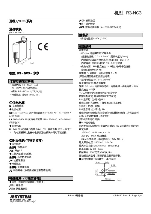
远程 I/O R3 系列通信模块机型: R3-NC3-①② ①、②在下列代码中选择。
(例如: R3-NC3-N/CE/W/Q)・特殊规格(例如: /C01/SET)①供电电源N: 无供电电源◆交流电源K3: 100~120V AC (允许电压范围 85~132V AC、47~66Hz)*(不符合CE)L3: 200~240V AC (允许电压范围 170~264V AC、47~66Hz)*(不符合CE)◆直流电源R:24V DC (允许电压范围 24V±10%、纹波系数 10%p-p以下)**、与电源模块以及备有电源的通信模块并用时不能选择。
②附加代码 (可指定多项)◆适用标准未填写: 不符合CE/CE: 符合CE◆三菱产双重PLC系统未填写: 不支持该系统/W: 支持该系统◆特殊规格未填写: 无特殊规格/Q: 特殊规格(从特殊规格之项另请选择)/C01: 硅涂层/C02: 聚氨酯涂层/C03: 橡胶涂层◆出厂时的设定/SET: 按照订购表格 (No: ESU-8422) 设定・CC-Link: 连接器型欧式端子盘 (适用电缆线: 0.2~2.5mm2、露线长度为7mm)・内部通信总线: 连接到底座 (机型: R3-BS□) 上・内部电源: 由底座 (机型: R3-BS□) 提供・供电电源、RUN接点输出: M3螺丝2块端子盘连接 (紧固扭矩为0.5N·m)压接端子: 请参照「适用压接端子」图(不能使用带绝缘套的压接端子)・适用电缆线: 0.75~1.25mm2端子螺丝材质: 铁表面镀镍隔离: CC-Link-内部通信总线・内部电源-供电电源-RUN接点输出-FG间主/从切换设定: 用侧面的DIP开关设定数据分配设定: 用侧面的DIP开关设定RUN显示灯: 红/绿2色LED通信正常时亮绿色灯;接收数据时亮红色灯(用DIP开关进行切换)ERR显示灯: 红/绿2色LED通信异常时绿色灯亮灯/闪烁 (电缆断线时熄灯,异常设定时闪烁);发送数据时,亮红色灯(用DIP开关进行切换)■RUN接点输出RUN接点: RUN显示灯亮绿色灯时ON (CC-Link通信正常时ON)额定负载: 250V AC 0.5A (cos ø = 1) 30V DC 0.5A (电阻负载) (满足EU指令时,额定负载小于50V AC。
SP333资料

s +5V Only, Single Supply Operation s Low Power Shutdown s 28-Pin SOIC Packagings 3 Drivers, 5 Receivers – RS-232s Complete AppleTalk™ Interface s High Data Rates10Mbps Differential Transceivers 460kbps Single-Ended TransceiversDESCRIPTION…The SP333 is a monolithic device that supports both Macintosh™ and PC serial interfaces.RS-232 mode offers three (3) RS-232 drivers and five (5) RS-232 receivers. Mac mode includes a differential driver and a single-ended inverting driver. Receivers in Mac mode include one differential receiver, one non-inverting single-ended receiver and one inverting single-ended receiver. An on-chip charge pump allows +5V-only operation, and a low power Shutdown mode makes the SP333 ideal for battery powered applications. The interface mode can be changed at any time by a mode select pin.These are stress ratings only and functional operation of the device at these ratings or any other above those indicated in the operation sections of the specifications below is not implied. Exposure to absolute maximum rating conditions for extended periods of time may affect reliability.V CC ...................................................................................................+12V Input VoltagesLogic........................................................-0.3V to (V CC +0.5V)Drivers..................................................-0.3V to (V CC +0.5V)Receivers..................................................................±15VDriver Outputs......................................................................................±14V Storage Temperature..................................................-65˚C to +150˚C Power Dissipation..........................................................................1000mWSPECIFICATIONS元器件交易网SPECIFICATIONS (CONTINUED)to T and V = 5V±5% unless otherwise noted.TC i r c u i tC i r c u i tFigure 5. Receiver Propagation DelaysTHEORY OF OPERATION...The SP333 is a single chip device that can be configured via software for either RS-232 or AppleTalk™ interface modes at any time. The SP333 is made up of three basic circuit ele-ments: single-ended drivers and receivers, dif-ferential drivers and receivers, and charge pump.APPLETALK™ DRIVERS/RECEIVERS...To program the SP333 for MacMode, Pin 25should be connected to a logic HIGH. In MacMode, the SP333 offers a complete AppleTalk serial interface.The driver section of the AppleTalk interface is made up of a differential driver and a single-ended inverting driver. The differential driver has voltage swings that are typically ±5V on each output pin under loaded conditions, and typically ±8V under no-load conditions. The differential driver can maintain ±3.6V (mini-mum) swings (per pin) under worst case load conditions of 450Ω between the differential output.The differential driver is equipped with a tri-state control pin. When TXEN is a logic LOW,the differential driver is active. When the TXEN pin is a logic HIGH, the differential driver functions in MacMode. The differential AppleTalk driver can support data rates up to 10Mbps.The single-ended AppleTalk driver also has typical voltage output swings of ±5V under loaded conditions, and ±8V under no-load con-ditions. The single-ended AppleTalk driver can maintain ±3.6V (minimum) swings under worst case conditions of 450Ω to ground. The single-ended AppleTalk driver can support data rates over 400kbps.The receiver section of the SP333 is made up of a differential receiver, a single-ended non-in-verting receiver , and a single-ended inverting receiver. The differential receiver has an input sensitivity of ±200mV over a common mode range of ±7V. The receivers have a typical input resistance of 15k Ω (12k Ω minimum). The differential receiver can receive data up to 10Mbps.The single-ended non-inverting receiver has a ±200mV input threshold, however, the input voltage can vary between ±7V. The typical input resistance of the single-ended non-invert-ing receiver is 15k Ω (12k Ω minimum). The single-ended non-inverting receiver can also receive data up to 10Mbps.The SP333 also has a single-ended inverting receiver input. This receiver is basically an RS-232 receiver (R5 receiver) and is typically used as a GPI (General Purpose Input) in the AppleTalk interface. The GPI input has TTL-compatible input thresholds that can receiveFigure 6. Receiver Enable and Disable Timesreceivers features 500mV of hysteresis margin to minimize the affects of noisy tranmission lines. The inputs also have a 5k Ω resistor to ground, in an open circuit situation the input of the receiver will be forced low, committing the output to a logic HIGH state. The input resis-tance will maintain 3k Ω-7k Ω over a ±15V range.The maximum operating voltage range for the receiver is ±30V, under these conditions the input current to the receiver must be limited to less than 100mA. Due to the on-chip ESD pro-tection circuitry, the receiver inputs will be clamped to ±15V levels; this should not affect operation at ±30Volts. The RS-232 receivers can operate over 400kbps.CHARGE PUMP...The charge pump is a Sipex-patented design (5,306,954) and uses a unique approach com-pared to older less-efficient designs. The charge pump still requires four external capacitors, but uses a four-phase voltage shifting technique to attain symmetrical 10V power supplies. The capacitor values of the SP333 can be as low as 0.1µF. Figure 11a shows the waveform found on the positive side of capacitor C2, and Figure 11b shows the negative side of capacitor C2.There is a free-running oscillator that controls the four phases of the voltage shifting. A de-scription of each phase follows.signals up to ±15V. The input resistance of the single-ended inverting receiver is typically 5k Ω(3k Ω to 7k Ω). The GPI receiver can operate up to 10Mbps.SINGLE ENDED DRIVERS/RECEIVERS...RS-232 (V.28) Drivers...The single-ended drivers and receivers comply the with the RS-232E and V.28 standards. The drivers are inverting transmitters which accept either TTL or CMOS inputs and output the RS-232 signals with an inverted sense relative to the input logic levels. Typically, the RS-232 driver output voltage swing is ±9V with no load and is guaranteed to be greater than ±5V under full load. The drivers rely on the V+ and V- voltages generated by the on-chip charge pump to main-tain proper RS-232 output levels. With worst case load conditions of 3k Ω and 2500pF, the four RS-232 drivers can still maintain ±5V output levels. The drivers can operate over 400kbps; the propagation delay from input to output is typically 1.5µs. During shutdown, the driver outputs will be put into a high impedance tri-state mode.RS-232 (V.28) Receivers...The RS-232 receivers convert RS-232 input signals to inverted TTL signals. Each of the fourFigure 9. Charge Pump Phase 3Figure 10. Charge Pump Phase 4元器件交易网Phase 1-Vss charge storage- During this phase of the clock cycle, the positive side of capacitors C1and C2 are initially charged to +5V. C1+ is then switched to ground and charge in C1- is trans-ferred to C2-. Since C2+ is connected to +5V,the voltage potential across capacitor C2 is now 10V.Phase 2-Vss transfer- Phase two of the clock connects the negative terminal of C2 to the Vss storage capacitor and the positive terminal of C2 to ground, and transfers the generated -10V to C3.Simultaneously, the positive side of capacitor C1 is switched to +5V and the negative side is connected to ground.Phase 3-Vdd charge storage- The third phase of the clock is identical to the first phase- the trans-ferred charge in C1 produces -5V in the negative terminal of C1, which is applied to the negative side of capacitor C2. Since C2+ is at +5V, the voltage potential across C2 is 10V.Phase 4-Vdd transfer- The fourth phase of the clock connects the negative terminal of C2 to ground the Vdd storage capacitor. Simultaneously with this, the positive side of capacitor C1 is switched to +5V and the negative side is connected to ground, and the cycle begins again.Since both V+ and V- are separately generated from Vcc in a no load condition, V+ and V- will be symmetrical. Older charge pump approaches that generate V- from V+ will show a decrease in the magnitude of V- compared to V+ due to the inherent inefficiencies in the design.The clock rate for the charge pump typically operates at 15kHz. The external capacitors should be 0.1µF with a 16V breakdown rating.External Power SuppliesFor applications that do not require +5V only,external supplies can be applied at the V+ and V- pins. The value of the external supply volt-ages must be no greater than ±10V. The current drain from the ±10V supplies is used for the RS-232 drivers. For the RS-232 driver, the current requirement is 3.5mA per driver. The external power supplies should provide a power supply sequence of either: +10V, –10V, and then +5V;or –10V, +10V, and then +5V. It is critical that the ±10V supplies are on before V CC.Figure 11. Charge Pump WaveformsShutdown ModeThe SP333 can be put into a low power shut-down mode by connecting the Shutdown pin (SD, Pin 26) to a logic HIGH. During Shut-down, the driver outputs are put into a high impedance tri-state, and the charge pump is put into stand-by mode. The supply current drops to less than 10µA during shutdown and can be activated in either RS-232 or AppleTalk mode. For normal operation, the SD pin should be connected to a logic LOW.Receiver EnableThe SP333 has a control line to enable or disable the receiver outputs. Pin 3 (RXEN) is active LOW; a logic LOW on Pin 3 will enable the receiver outputs. A logic HIGH on Pin 3 will disable the receiver outputs. The receiver en-able function can be initiated in either RS-232 or AppleTalk mode.Wake-UpThe SP333 also features a "wake-up" function. The wake up function allows the RS-232 receiv-ers to remain active during Shutdown mode unless they are disabled by the Receiver Enable control pin (Pin 3). The wake-up feature allows users to take advantage of the low power Shut-down mode and keep the receivers active to accept an incoming "ring indicator" signal.ORDERING INFORMATIONModel Temperature Range Package Types SP333CT..............................................................................0˚C to +70˚C.........................................................................................28-Pin SOIC SP333ET.............................................................................-40˚C to +85˚C........................................................................................28-Pin SOIC。
MC33035中文

0.1
0.2
0.3
电源电流
ICC
--
12
16
mA
管脚 17 (VCC = VC = 20 V)
IC
--
14
20 0
管脚 17 ( VCC = 20 V, VC = 30 V)
--
3.5
6.0
管脚 18 ( VCC = VC = 20 V)
--
5.0
10
管脚 18 (VCC = 20 V, VC = 30 V)
ISC
40
75
–
mA
基准欠电压锁定阈值
Vth
4.0
4.5
5.0
V
误差放大器
输入偏移电压 (TA = –40° ~ +85°C)
VIO
--
0.4
10
mV
输入偏移电流 (TA = –40°∼+85°C)
IIO
--
8.0
500
nA
输入偏置电流 (TA = –40° ~ +85°C)
IIB
--
-46
-1000 nA
tHl ,低速驱 动响应 时间
图11,低速驱动响应时间 VS电流感应输入电压
250
VCC=20V
VC=20V
200
RL=∞
CT=10nF
150
TA=25℃
100
50
0 1.0
2.0 3.0 4.0 5.0 6.07.0 10 电流感应输入电压(标称为 Vth)
V sa t,输出饱 和电压 (V)
图12,fault输出饱和电压 VS陷电流
Vsat,输出饱和电压(V)
GR100使用说明书.
GR100电力监控仪操作手册珠海格锐电子有限公司目录简介 2 电量测量 4 开关量监测 6 控制输出7 电气接线8 操作说明10 通讯连接18 外形\开孔尺寸19 技术参数21G R100电力监控仪是一种简单可靠的测控装置,可以广泛应用于电力系统、环境监控、低压配电等自动化领域。
GR100具有如下优点:电力参数采集GR100可以满足各种场合下对电力参数采集的需求,具有极佳的性能价格比。
通过一台装置可以完全代替所有的传统电量变送器。
GR100可以实时提供三相电压、三相电流、三相功率及总计、三相功率因数、频率、电度等许多参量,完全符合用户对现场电力参数采集的需求。
开关节点状态监测GR100提供灵活的可配置的四路节点输入,适用于监测断路器位置信号、刀闸、开关位置信号等状态信息。
在低压配电网络中,基本可以实现一回线路状态量监测的需求。
节点输入电压可选择,即可选用仪表内部开出的低压电源,也可以适用外部高压电源的输入要求。
灵活的继电器控制模式GR100可以提供4路继电器输出信号,支持最高可达250Vac/10A或30Vdc/10A的节点容量。
继电器输出脉冲可整定,动作时间可整定。
有就地监控和远方遥控两种模式。
数据查询功能GR100提供两种方式供用户查询实时监测的数据量:·显示通过独立单元的显示模块,用户可以任意查询所关心的数据;并且可以进行现场的编程,调整仪表的工作参数·通讯采用RS485通讯接口,方便用户进行网络通讯;与MODBUS-RTU标准完全兼容,并且提供开放式的协议标准,方便第三方进行开发界面友好该功能在用户配置显示单元时有效,用户可以方便的通过显示单元查询数据或者是进行现场设置参数并进行编程运行方便全部的测量值、整定值都可以通过本地或者是通过RS485通讯口存取稳定可靠采用了多种抗干扰和保护措施,保证设备长期工作的稳定性、可靠性说明GR100按操作要求来显示测量值,显示一次回路的电量参数为:电压·测量相电压Va,Vb和Vc以及平均值·测量或计算线电压Uab,Ubc和Uca以及平均值电流·测量电流Ia,Ib和Ic以及平均值有功功率·计算三相有功功率Pa,Pb,Pc以及总和无功功率·计算三相无功功率Qa,Qb,Qc以及总和功率因数·计算三相功率因数PFa,PFb,PFc以及三相总值视在功率·计算三相视在功率Sa,Sb,Sc以及总和频率·测量并计算三相频率电度·计算三相总输入、输出有功电度以及净值·计算三相总输入、输出无功电度以及净值·计算三相总视在电度其它·可以接受用户定制需要计算的电参量,有关具体细节内容请与公司联系电压测量当系统电压等级小于347V(相)/600V(线)时,GR100电压测量回路可以直接接入系统。
松下A5电机样本
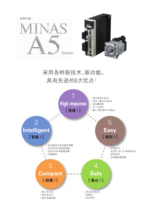
ĿӬᄰ7ಪҮ٧ʿၸnj ŀឯҫॸࠃᬄᜈᎵᆷᝢࠪ̅'ᅮᫍϢႂಪᄉ
ͤnj
ቿՋ SNJO .4.& ۋႂ 8 ̾ʽ
ᄉణᰳᣀᤳ SNJOnj
NJǏ8 ளேඊǐ
ᣀᅽ </eN>
" ጆѴNJ.4.%ὉὉὉ
ͮᎵૈ̽ᤳऎ<SNJO> Ժԟஜ
Ԫఝథௐᫍ
ႂ
ᤁᣀ
Ϣൢ
ᤳ
ऎ
ኃܘᄝ
ኃܘᄝ ኃܘᄝ
థ
థ
థ
ܰᦉ࣯ҩᑞ
ѽၸܰᦉ࣯٧࠱ਆᄉܰᦉ࣯ᣀᅽਆϘҪڙ ˀᣀᅽૈ̽ᄰક๖ᄉழՓʼὋђ࠵࣯ᦉܰځᣀᅽᏪ࠭ ᒰᄉॕֽὋ̯ᏪᬋͯᤳऎNjђ࠵Үᄉҩᑞnj
ʿၸܰᦉ࣯
nj
4
MSMA 2kW MSME 2kW
〈例:MSM、MDM 时〉 系列 A4 A5 轻量化
MSM 1kW 4.5kg 3.5kg ▲1kg MSM 2kW 6.5kg 5.3kg ▲1.2kg MDM 1kW 6.8kg 5.2kg ▲1.6kg MDM 2kW 10.6kg 8.0kg ▲2.6kg
ႂຸуѣႂึં҃ҩᑞ Dž˝ൢଋႂຸௐځуѣႂึᤴᄉႂຸறᡸ٧Ѭ
றὋЮᎵ˿уѣႂึં҃ႂ٧nj
表1 适用线性标尺
并用
Sony Manufacturing Systems 株式会社制造
串行式(绝对值)
株式会社三丰制造
Sony Manufacturing Systems 株式会社制造
ൣݝὀ
$PNQBDU
ǗᣏΦ ǘ
ளࢹͺழก ளधԦᔆ ளधԦᎃᆉ٧
睿英电气RM系列数字式电动机综合保护装置
RM030
RM050
RM100
RM150
RM200
型号
工作电压 频率 三相
功率因数保护
谐波测量保护
温度测量保护
功率保护
欠/过电流保护
保护功能
缺相保护 不平衡保护
逆相保护
堵转保护
短路保护
接地保护
失速保护
通讯MODBUS 4~20mA输出
产品概述,功能与特点·······················································································2 型号选择················································································································3 安装尺寸················································································································5 接线端子,指示灯说明·······················································································6 接线图····················································································································6 技术指标················································································································7
DPR330L系列数字式线路保护装置说明书6

4.1 DPR331L数字式线路保护装置定值...................................................... 32
7 使用说明.............................................................................. 63
7.1 按键功能介绍....................................................................... 63 7.2 面板布置说明....................................................................... 63 7.3 命令菜单使用说明................................................................... 64
电压切换回路
√
√
√
─
注:√:表示具有本项功能;─ :表示无此项功能。 DPR331L、DPR332L 数字式线路保护装置适用于大电流接地系统的配电线路。 DPR333L 数字式线路保护装置适用于小电流接地系统的配电线路。 DPR321L 数字式线路保护装置适用于选择性要求高的重要联络线路、重要负荷线路。
6 背板端子图............................................................................ 52
朗睿 LR035AR F系列彩色工业液晶显示器 说明书

LR035AR/F系列 彩色工业液晶显示器使用说明书上海朗睿电子科技有限公司本说明书仅适用于朗睿科技公司生产的LR035AR/F系列液晶显示器本公司产品已经通过ISO9001:2000质量体系认证!亲爱的用户:感谢您购买朗睿科技研制生产的LR035AR/F系列工业彩色液晶显示器!在您使用本产品前,请务必仔细阅读本使用说明书。
您能成为我们的用户,是我们莫大的荣幸。
为了使您尽快掌握朗睿液晶显示器的使用方法,我们特别为您编写了此说明书。
我们对产品说明书的编排力求全面而简捷。
从中您可以获得有关朗睿科技公司LR系列 3.5英寸工业彩色液晶显示器产品的配置、性能、操作的基本使用方法等方面的一些知识。
我们强烈建议您在使用本显示器之前,务必先仔细阅读,这会有助于您更好地使用本显示器。
如果您未按本说明书的要求操作显示器而由此引起的任何损失,朗睿科技公司将不承担责任。
我们已经尽我们最大的努力尽量避免人为的失误,以确保本说明书中所提供的信息是正确可靠的,但我们不能完全保证:不会有在印刷之前未曾发现或检查出的差错,以及那些我们无法控制环节上的疏漏,请您多加包涵!有时,我们为了提高显示器的整机性能和可靠性,可能会对产品的硬件和软件做一些小的调整,这样有可能会导致机器的实际情况与说明书有某些不一样的地方,但这不会实质性地影响您对显示器的使用,请您能够谅解!谢谢您的合作!朗睿科技公司目 录第一章简介 (3)1.1TFT LCD常用信号解释: (3)1.2特点 (3)1.3系统结构框图 (5)第二章性能与接口 (6)2.1性能参数 (6)2.2外部接口 (7)2.3拨码开关设置 (8)2.4通讯接口连线图 (9)第三章连接与通讯 (10)3.1连接方法 (10)3.2串行通讯 (10)3.3并行通讯 (13)第四章命令详解 (13)4.1命令详解 (13)4.2命令的位置 (33)第五章应用举例 (35)附录一、51汇编程序样例 (37)附录二、51汇编(并口)程序举例 (39)附录三、ASCII对照表 (41)第六章机械结构 (43)第七章其它 (44)一、售后支持说明 (44)二、运输损坏处理 (44)三、显示器的存储 (44)四、注意事项 (45)五、控制电路的注意事项 (46)第八章彩色LCD产品编码 (47)彩色LCD产品编码 (47)产品型号信息提取 (48)第一章简介本说明书提供了您所使用朗睿科技公司LR035AR/F系列工业液晶显示器的硬件和软件信息。
美特尔 AM-33 3 3 4 数字智能一键自动DMM操作手册安全规则说明书

AM-333 3/4 DIGITS INTELLIGENT ONESWITCH AUTO DMMOPERATION MANUALSAFETY RULESλThis meter is designed and tested in accordance with IEC publication 1010, pollution degree II and installation category (overvoltage category) III 600V.λThis meter has been tested according to the following EC Directives♦89/336/EEC (EMC of Nov., 1992, Electromagnetic Compatibility)♦73/23/EEC (Product safety law of June 11, 1979, Low Voltage Directive of February 19, 1973)λThis meter is designed to be indoor use at temperature 41°F to 104°F (5°C to 40°C) and altitude up to 2,000m.λTo ensure that the meter is used safely, follow all safety and operating instructions in this operation manual. If the meter is not used as described in this operation manual, the safety features of this meter might be impaired.λDo not use the meter if the meter or test leads look damaged, or if you suspect that the meter is not operating properly.λWhen using the probes, keep your fingers behind the finger guards on the probes.λDisconnect the live test lead before disconnecting the common test lead.λMake sure power is off before cutting, unsoldering, or breaking the circuit. Small amount of current can be dangerous.λDo not apply more than 600Vdc or 600Vac rms between a terminal and earth ground.λTo avoid electrical shock, use CAUTION when working above 60Vdc or 25Vac rms.Such voltages pose a shock hazard.λNever make measurements with the battery cover or bottom case off.λTo avoid electrical shock or damage to the meter, do not exceed the input limits. INTERNATIONAL SYMBOLSImportant informationsee manual ContinuityAC GroundDC Double insulation FEATURESλOne switch operation.λAuto polarity with engineering units annunciator.λDC volt, AC volt, Resistance(4V threshold voltage to determine V or R function)λContinuity testλAuto power off with power resumeλData holdλFull range 600V overload protectionλConform to IEC1010-1 CAT III 600V3.1 General SpecificationsDisplay: 3 3/4 digit LCD, 3999 counts with decimal point andengineering units annunciator displayPolarity:Automatic, (-) negative polarity indication.Zero adjustment:Automatic.Measuring Method:Dual slop integration A to D converter system.Over range indication:Only the “OL” is displayed.Power:Single, standard 9 volt battery NEDA 1604, JIS 006P,IEC6F22.Dimension:70 (H) x 144 (W) x 40 (D) mm.Weight:Approx. 270gm. (including batteries and packaging)3.2 Electrical SpecificationsPANEL DESCRIPTIONS1) 3 3/4 digit LCD display2) Power resume button3) ON/OFF switch4) Data hold button5) Case6) Input and common terminals WARNINGOPERATION1) When measuring voltage ensure that the instrument is not connected. Always ensure thatthe correct terminals are used for the type of measurement to be made.2) Use extreme care when measuring voltage above 50V, especially from sources wherehigh energy exists.3) Avoid making connections to “live” circuits whenever possible.4) When making current measurements ensure that the circuit is not “live” before opening itin order to connect the test leads.5) Before making resistance measurements or continuity test, ensure that the circuit undertest is de-energised.6) Extreme care should be taken when using the instrument to conjunction with a currenttransformer connected to the terminals. High voltage may be produced at the terminals if an open circuit occurs.7) Ensure that the test leads and prods are in good condition with no damage to theinsulation.8) Take care not to exceed the over-load limits as given in the specifications.9) Fuse for replacement must be of the correct type and rating.5.1 DC and AC Voltage measurement1)Connect the black test lead to the “COM” socket and red test lead to the “ ” socket.2) Connect the test prods across the source or load under measurement.5.2 Resistance measurement1) Connect the black test lead to the “COM” socket and red test lead to the “ ” socket.2) Connect the prods across the circuit to be tested.CAUTION: Ensure that the circuit to be tested is “dead”.Max. input over-load : 600V rms < 30sec.5.3 Continuity test1) Connect the black test lead to the “COM” socket and red test lead to the “ ” socket.2) Connect the prods across the circuit to be tested, if the resistance less than approx. 47Ω,buzzer will be activated.5.4 Data holdA push switch is used to hold data during measurement. Pressing the key, reading is heldand “H” appears on display. Pressing the switch again to release the hold data.Note : In auto AC/DC voltage selection, if the source under test is AC, hold function willoperative only when source under test is in continuous contact with the test probes.5.5 Auto power offThe meter will turn off automatically to extend the battery life after approx. 30 minutes withoutoperation. Resume power by pressing “P. Resume” button.6. MAINTENANCECAUTIONBEFORE ATTEMPTING BATTERY AND FUSE REMOVAL OR REPLACEMENT,DISCONNECT TEST LEADS FROM ANY ENERGISED CIRCUITS TO AVOID SHOCKHAZARD.6.1 Fitting and replacing the battery1) Ensure that the instrument is not connected to any external circuit, switch off the meterand remove the test leads from the terminals.2) Remove the screw of the back case.3) Replace the spent battery with the same type.4) Reinstate the back case, tighten and securing screw.6.2 CleaningPeriodically wipe the case with a soft damp cloth and mild household cleanser. Do not useabrasives or solvents. Ensure that no water gets inside the equipment to prevent possibleshorts and damage.FOR TECHNICAL ASSISTANCE,PLEASE CONTACT:AMPROBETel : 305-423-7500Fax : 305-423-7554Technical Support : 800-327-5060!!!。
INA333 微功耗、零漂移、轨到轨输出仪表放大器说明书

V OUTREFR GProduct FolderSample &BuyTechnical Documents Tools &SoftwareSupport &CommunityINA333ZHCSAK0C –JULY 2008–REVISED DECEMBER 2015INA333微功耗(50μA)、零漂移、轨到轨输出仪表放大器1特性•低偏移电压:25µV (最大值),G ≥100•低漂移:0.1μV/°C ,G ≥100•低噪声:50nV/√Hz ,G ≥100•高共模抑制比(CMRR):100dB (最小值),G ≥10•低输入偏置电流:200pA (最大值)•电源范围:1.8V 至5.5V•输入电压:(V–)+0.1V 至(V+)–0.1V •输出电压:(V–)+0.05V 至(V+)–0.05V •低静态电流:50μA•工作温度范围:-40°C 至+125°C •已过滤射频干扰(RFI)的输入•8引脚VSSOP 和8引脚WSON 封装2应用范围•桥式放大器•心电图(ECG)放大器•压力传感器•医疗仪表•便携式仪表•衡器•热电偶放大器•电阻式温度检测器(RTD)传感器放大器•数据采集3说明INA333器件是一款低功耗的精密仪表放大器,具有出色的精度。
该器件采用通用的三运算放大器设计,并且拥有小巧尺寸和低功耗特性,非常适合各类便携式应用。
可通过单个外部电阻在1到1000范围内设置增益。
INA333设计为采用符合行业标准的增益公式:G =1+(100k Ω/R G )。
INA333器件拥有超低的偏移电压(25μV ,G ≥100),出色的偏移电压漂移(0.1μV/°C ,G ≥100),以及较高的共模抑制比(100dB ,G ≥10)。
该器件可由低至1.8V (±0.9V)的电源供电运行,静态电流仅为50μA ,因此非常适合电池供电类系统。
上海朗睿电子 LR035AR F 工业彩色液晶显示器 说明书
3
GND
地
13
STB
选通信号
下降沿有效
(并 口 )
4
BUSY
忙信号 高电平有
14
RXD
接收数据
RS232
效 (并 口 )
5
DATA7
并口数据 并口
15
DTR
缓冲区满
RS232
6
DATA6
并口数据 并口
16
BLC
关背光显示 低电平有效
7
DATA5
并口数据 并口
17
RESET
复位
低电平有效
8
DATA4
并口数据 并口
LR035AR/F
工业彩色液晶显示器
使 用 说 明 书
上海朗睿电子科技有限公司
本 公 司 已 通 过 ISO9001: 2008质 量 体 系 认 证 !
LR035AR/F 系 列 工 业 液 晶 显 示 器 使 用 说 明 书 V3.3
L﹠ L 朗 睿
亲爱的用户:
感 谢 您 购 买 我 公 司 研 制 生 产 的 LR035AR/F彩 色 工 业 液 晶 显 示 器 ! 在您使用本产品前,请务必仔细阅读本使用说明书。
255 幅
190(+/- 10)mA/5V
关 闭 背 光 120(+/- 10)mA/5V
-20℃ ~ +70℃
-30℃ ~ +80℃
LED
/
模组安装方式
模组安装实物图
-5-
LR035AR/F 系 列 工 业 液 晶 显 示 器 使 用 说 明 书 V3.3
4、 产 品 结 构 尺 寸 图
L﹠ L 朗 睿
NCR-333航行警告仪操作指南

NCR-333航行警告仪操作说明按MENU键显示主菜单按上下方向键▲▼选择菜单,按ENT键或右方向键显示选择的菜单。
按CLR键显示前一个页面。
菜单说明如下:1.RX STA TION: 接收站台选择2.MESSAGE TYPE: 接收信息类型选择3.DISPLAY: 显示设置4.NA VTEX: NA VTEX接收设置5.MAINTENANCE: 维护菜单6.LANGUAGE: 语言选择[EXIT]: 退出菜单1、接收站台选择(RX STA TION)要选择接收站台,进入1.RX STATION菜单(1)接收模式选择(RX MODE){自动模式和手动模式}➢AUTO:自动模式在自动模式下自动确定位置和接收海区。
➢MANUAL:手动模式手动选择接受的站台(2)接受频道的选择(OPERA TING FREQ)三个频段:RX1(518KHZ)、RX2(490KHZ)、RX3(4209.5KHZ)(3)自动选择接受站台(AUTO MODE SETTING)在每个海区中选择对应频道的站台:➢选择接受的站台选择NA V AREA,按下ENT键,再按▲▼键选择NA V AREA的数目;然后选择FREQUENCY按下ENT键选定频率;最后选择要接受的站台按ENT键。
➢取消设置按下CLR/MENU/DISP/USER键,再弹出的对话框中选择OK就取消了设置➢设置下个频道或海区与选择接受站台的步骤类同。
➢保存设置按下*键,在弹出对话框中选择OK按ENT键(4)手动选择接受站台(MANUAL MODE SETTING)手动中没有了NA V AREA选项,其他的操作与自动类同。
2、接收信息类型选择(MESSAGE TYPE)要选择接受信息类型,进入2. MESSAGE TPYE SETTING根据自己的情况在列表中选择所需的信息类型,具体的操作与AUTO MODE SETTING 一致。
3、显示设置(DISPLAY)要对显示进行调整,进入3.DISPLAYa)对比度的设置(CONTRAST)当选择CONTRAST后,按▲▼键选择对比度1~13,然后按ENT键确认。
- 1、下载文档前请自行甄别文档内容的完整性,平台不提供额外的编辑、内容补充、找答案等附加服务。
- 2、"仅部分预览"的文档,不可在线预览部分如存在完整性等问题,可反馈申请退款(可完整预览的文档不适用该条件!)。
- 3、如文档侵犯您的权益,请联系客服反馈,我们会尽快为您处理(人工客服工作时间:9:00-18:30)。
Operating Temperature Range-40 ~ +85°C-25 ~ +85°C Rated Voltage Range10 ~ 250Vdc315 ~ 450Vdc Rated Capacitance Range180 ~ 82,000µF56 ~ 1,000µF Capacitance Tolerance±20% (M)
Max. Leakage Current (µA)
After 5 minutes (20°C)
3 x C(µF)V
Max. Tan δat 120Hz/20°C W.V. (Vdc)10162535506380100160~400420~450 Tan δ max.0.550.500.450.400.350.300.250.200.150.25
Surge Voltage W.V. (Vdc)1016
2535506380100160180 S.V. (Vdc)132032446379100125200220 W.V. (Vdc)200220250315350385400420450-S.V. (Vdc)250270300365400435450470500-
Ripple Current Correction Factors
Frequency (Hz)50 (60)1205001K10K>-----Multiplier
at 85°C
10 ~ 100Vdc0.90 1.00 1.05 1.10 1.15-----
160 ~ 250Vdc0.80 1.00 1.20 1.30 1.50-----
315 ~ 450Vdc0.80 1.00 1.20 1.25 1.40-----
Low Temperature Stability (10 to 250Vdc)
Temperature (°C)0-25-40-------Capacitance Change-5%-15%-30%-------Impedance Ratio 1.5312-------
Load Life Test 3,000 hours at +85°C Capacitance Change Within ±20% of initial measured value Tan δLess than 200% of specifi ed maximum value Leakage Current Less than specifi ed maximum value
Shelf Life Test 1,000 hours at +85°C
(no load)Capacitance Change Within ±20% of initial measured value Tan δLess than 200% of specifi ed maximum value Leakage Current Less than specifi ed maximum value
Surge Voltage Test
Per JIS-C-5141 (table #6, #4) Surge voltage applied: 30 seconds "On" and 5.5 minutes no voltage "Off"Capacitance Change Within ±20% of initial measured value Tan δLess than 200% of specifi ed maximum value Leakage Current Less than specifi ed maximum value
Soldering Effect Refer to JISC5102.8.5Capacitance Change Within ±10% of initial measured value Tan δLess than specifi ed maximum value Leakage Current Less than specifi
ed maximum value
Large Can Aluminum Electrolytic Capacitors NRLR Series FEATURES
• EXPANDED VALUE RANGE
• LONG LIFE AT +85°C (3,000 HOURS)
• HIGH RIPPLE CURRENT
• LOW PROFILE, HIGH DENSITY DESIGN
• SUITABLE FOR SWITCHING POWER SUPPLIES
SPECIFICATIONS
MECHANICAL CHARACTERISTICS:
1. Safety Vent:
The capacitors are provided with a pressure sensitive safety vent on the top of can. The vent is designed to rupture in the event that high internal gas pressure is developed by circuit mal f unc t ion or mis-use like reverse voltage.
2. Terminal Strength:
Each terminal of the capacitor shall withstand an axial pull force of 4.5Kg for a period 10 seconds or a radial bent force of 2.5Kg for a period
of 30 seconds.
NRLR 222 M 50V 20X25 S F
RoHS compliant
Lead Length (S=4mm, L=6mm)
Case Size (mm)
Voltage Rating
Tolerance Code
Capacitance Code
Series
PART NUMBER SYSTEM
PRECAUTIONS
Please review the notes on correct use, safety and precautions found on pages T10 & T11
of NIC’s Electrolytic Capacitor catalog.
Notice for Mounting
The space from the top of the can shall be more than (3mm) from chassis or
Recommended PC Board Mounting Holes: Sleeve Color: Dark Blue
Can Top Safety Vent
Insulation Sleeve and Minus
Polarity Marking
D+1
Max.
L ± 2 4.0 ± 1
or
6.3 ± 1
10
(-)
(+)
SAFETY VENT
∅= 2
Chassis
RoHS
Compliant
includes all homogeneous materials
*See Part Number System for Details
Large Can Aluminum Electrolytic Capacitors NRLR Series
Large Can Aluminum Electrolytic Capacitors NRLR Series
Large Can Aluminum Electrolytic Capacitors NRLR Series
Large Can Aluminum Electrolytic Capacitors NRLR Series
Large Can Aluminum Electrolytic Capacitors NRLR Series
Large Can Aluminum Electrolytic Capacitors NRLR Series
Large Can Aluminum Electrolytic Capacitors NRLR Series
Large Can Aluminum Electrolytic Capacitors NRLR Series
Large Can Aluminum Electrolytic Capacitors NRLR Series STANDARD PRODUCT LIST, CASE SIZE AND SPECIFICATIONS
160
Large Can Aluminum Electrolytic Capacitors
NRLR Series
6.0mm - Optional Lead Length
元器件交易网。