Synaptic Plasticity of Feeding Circuits Hormones and Hysteresis
生物工程生物技术专业英语翻译(二)

第二章生长与代谢的生物化学2.1 前言一个微生物以生产另一个微生物为目的。
在某些情况下,利用微生物的生物学家们希望这样的情况能够快速频繁的发生。
在另外一些产物不是生物体自身的情况下,生物学家必须对它进行操纵使微生物的目标发生变化,这样以来,微生物就要努力的挣脱对它们繁殖能力的限制,生产出生物学家希望得到的产物。
生物体的生长过程及其生产出的各种产物与微生物代谢的本质特点是密不可分的。
代谢过程是两种互相紧密联系又以相反方向进行的活动过程。
合成代谢过程主要是细胞物质的生成,不仅包括构成细胞的主要组成物质(蛋白质、核酸、脂质、碳水化合物等等),同时也包括它们的前提物质——氨基酸、嘌呤与嘧啶、脂肪酸、各种糖与糖苷。
合成代谢不是自发进行的,必须由能量所推动,对大多数微生物来说,是通过一系列的产能分解代谢过程来供给能量。
碳水化合物分解为CO2和水的过程是最为常见的分解代谢反应,然而微生物以这样的方式还能够利用更大范围的还原性含碳化合物。
分解代谢与合成代谢所有微生物生物化学的基础,可以从两者的平衡关系或者分别对它们进行讨论。
实际中,我们要有效的区分那些需要空气中的氧进行需氧代谢的生物与那些进行厌氧代谢的生物。
还原性含碳化合物与O2反应生成水和CO2,这是一个高效的放热反应过程。
因此,一个进行需氧代谢的生物要使用一小部分底物进行分解代谢以维持某一水平的合成代谢,即成长过程。
对于厌氧型生物,其底物的转化的过程基本上是一个不匀称的反应(氧化还原反应),产生很少的能量,因此,大部分底物都要被分解从而维持一定水平的合成代谢。
在生物体中这种差别能够明显的体现出来,比如酵母,它属于兼性厌氧生物,即它可在有氧条件下生长也可在无氧环境下生存。
需氧酵母使糖以同样的速度转化为CO 2和水,相对产生高产量的新酵母。
而厌氧条件下,酵母菌生长缓慢,此时酵母被有效的转化为酒精和CO 2。
2.2 代谢与能量分解代谢与合成代谢间的有效联系在于,各种分解代谢过程促进少量反应物的合成,而后又被用来促进全面的合成代谢反应。
7衰老动物模型

SAM种系寿命及老化病态特征 ( )
二、鱼类衰老动物模型
虹鳚鱼(guppy) 斑马鱼(zebrafish) 鱂鱼(killifish)
3.γ射线辐照的衰老大鼠模型
让大鼠辐照γ射线能使机体内产生多种自由基,与生物膜中 不饱和脂肪酸的弱键和不饱和键有高度的亲和力,启动脂质 过氧化物反应链;辐射能使氧化酶和非氧化酶活性系统的防 御机制减弱,白细胞总数和血红蛋白明显降低。 大鼠的辐照吸收剂量为3Gy较为理想,辐照面积为25× 25 cm2,辐照源距动物高度为80cm,每次辐照为4min 53s, 连续辐照5d能快速有效的建立衰老动物模型。 基于衰老自由基学说,把SOD和MDA作为衰老的生物学指标, 辐射后大鼠可作为理想的测定衰老生化指标变化的动物模型。 该法操作较简单,时间较D-半乳糖致衰老模型短,是一种快 速有效建立衰老动物模型的方法。
快速老化模型鼠的分类及特点
SAM系统以老化为主要特征,根据老化的速度分为快速 老化系(senescence accelerated mouse/prone, SAM-P)及抗快速老化系(se-nescence accelerated mouse/resistance,SAM-R)。
SAM-R系统:包括3个亚系SAM-R/1、SAM-R/2、 SAM-R/4。
复习思考题
大鼠衰老模型有哪几种?简述其与衰老学说的关系。
简述臭氧损伤衰老模型的理论基础和检测指标。 简述快速老化模型鼠的分类与应用。
半导体制造技术
Semiconductor Manufacturing Technology半导体制造技术Instructor’s ManualMichael QuirkJulian SerdaCopyright Prentice HallTable of Contents目录OverviewI. Chapter1. Semiconductor industry overview2. Semiconductor materials3. Device technologies—IC families4. Silicon and wafer preparation5. Chemicals in the industry6. Contamination control7. Process metrology8. Process gas controls9. IC fabrication overview10. Oxidation11. Deposition12. Metallization13. Photoresist14. Exposure15. Develop16. Etch17. Ion implant18. Polish19. Test20. Assembly and packagingII. Answers to End-of-Chapter Review QuestionsIII. Test Bank (supplied on diskette)IV. Chapter illustrations, tables, bulleted lists and major topics (supplied on CD-ROM)Notes to Instructors:1)The chapter overview provides a concise summary of the main topics in each chapter.2)The correct answer for each test bank question is highlighted in bold. Test bankquestions are based on the end-of-chapter questions. If a student studies the end-of-chapter questions (which are linked to the italicized words in each chapter), then they will be successful on the test bank questions.2Chapter 1Introduction to the Semiconductor Industry Die:管芯 defective:有缺陷的Development of an Industry•The roots of the electronic industry are based on the vacuum tube and early use of silicon for signal transmission prior to World War II. The first electronic computer, the ENIAC, wasdeveloped at the University of Pennsylvania during World War II.•William Shockley, John Bardeen and Walter Brattain invented the solid-state transistor at Bell Telephone Laboratories on December 16, 1947. The semiconductor industry grew rapidly in the 1950s to commercialize the new transistor technology, with many early pioneers working inSilicon Valley in Northern California.Circuit Integration•The first integrated circuit, or IC, was independently co-invented by Jack Kilby at Texas Instruments and Robert Noyce at Fairchild Semiconductor in 1959. An IC integrates multiple electronic components on one substrate of silicon.•Circuit integration eras are: small scale integration (SSI) with 2 - 50 components, medium scale integration (MSI) with 50 – 5k components, large scale integration (LSI) with 5k to 100kcomponents, very large scale integration (VLSI) with 100k to 1M components, and ultra large scale integration (ULSI) with > 1M components.1IC Fabrication•Chips (or die) are fabricated on a thin slice of silicon, known as a wafer (or substrate). Wafers are fabricated in a facility known as a wafer fab, or simply fab.•The five stages of IC fabrication are:Wafer preparation: silicon is purified and prepared into wafers.Wafer fabrication: microchips are fabricated in a wafer fab by either a merchant chip supplier, captive chip producer, fabless company or foundry.Wafer test: Each individual die is probed and electrically tested to sort for good or bad chips.Assembly and packaging: Each individual die is assembled into its electronic package.Final test: Each packaged IC undergoes final electrical test.•Key semiconductor trends are:Increase in chip performance through reduced critical dimensions (CD), more components per chip (Moore’s law, which predicts the doubling of components every 18-24 months) andreduced power consumption.Increase in chip reliability during usage.Reduction in chip price, with an estimated price reduction of 100 million times for the 50 years prior to 1996.The Electronic Era•The 1950s saw the development of many different types of transistor technology, and lead to the development of the silicon age.•The 1960s were an era of process development to begin the integration of ICs, with many new chip-manufacturing companies.•The 1970s were the era of medium-scale integration and saw increased competition in the industry, the development of the microprocessor and the development of equipment technology. •The 1980s introduced automation into the wafer fab and improvements in manufacturing efficiency and product quality.•The 1990s were the ULSI integration era with the volume production of a wide range of ICs with sub-micron geometries.Career paths•There are a wide range of career paths in semiconductor manufacturing, including technician, engineer and management.2Chapter 2 Characteristics of Semiconductor MaterialsAtomic Structure•The atomic model has three types of particles: neutral neutrons(不带电的中子), positively charged protons(带正电的质子)in the nucleus and negatively charged electrons(带负电的核外电子) that orbit the nucleus. Outermost electrons are in the valence shell, and influence the chemical and physical properties of the atom. Ions form when an atom gains or loses one or more electrons.The Periodic Table•The periodic table lists all known elements. The group number of the periodic table represents the number of valence shell electrons of the element. We are primarily concerned with group numbers IA through VIIIA.•Ionic bonds are formed when valence shell electrons are transferred from the atoms of one element to another. Unstable atoms (e.g., group VIIIA atoms because they lack one electron) easily form ionic bonds.•Covalent bonds have atoms of different elements that share valence shell electrons.3Classifying Materials•There are three difference classes of materials:ConductorsInsulatorsSemiconductors•Conductor materials have low resistance to current flow, such as copper. Insulators have high resistance to current flow. Capacitance is the storage of electrical charge on two conductive plates separated by a dielectric material. The quality of the insulation material between the plates is the dielectric constant. Semiconductor materials can function as either a conductor or insulator.Silicon•Silicon is an elemental semiconductor material because of four valence shell electrons. It occurs in nature as silica and is refined and purified to make wafers.•Pure silicon is intrinsic silicon. The silicon atoms bond together in covalent bonds, which defines many of silicon’s properties. Silicon atoms bond together in set, repeatable patterns, referred to asa crystal.•Germanium was the first semiconductor material used to make chips, but it was soon replaced by silicon. The reasons for this change are:Abundance of siliconHigher melting temperature for wider processing rangeWide temperature range during semiconductor usageNatural growth of silicon dioxide•Silicon dioxide (SiO2) is a high quality, stable electrical insulator material that also serves as a good chemical barrier to protect silicon from external contaminants. The ability to grow stable, thin SiO2 is fundamental to the fabrication of Metal-Oxide-Semiconductor (MOS) devices. •Doping increases silicon conductivity by adding small amounts of other elements. Common dopant elements are from trivalent, p-type Group IIIA (boron) and pentavalent, n-type Group VA (phosphorus, arsenic and antimony).•It is the junction between the n-type and p-type doped regions (referred to as a pn junction) that permit silicon to function as a semiconductor.4Alternative Semiconductor Materials•The alternative semiconductor materials are primarily the compound semiconductors. They are formed from Group IIIA and Group VA (referred to as III-V compounds). An example is gallium arsenide (GaAs).•Some alternative semiconductors come from Group IIA and VIA, referred to as II-VI compounds. •GaAs is the most common III-V compound semiconductor material. GaAs ICs have greater electron mobility, and therefore are faster than ICs made with silicon. GaAs ICs also have higher radiation hardness than silicon, which is better for space and military applications. The primary disadvantage of GaAs is the lack of a natural oxide.5Chapter 3Device TechnologiesCircuit Types•There are two basic types of circuits: analog and digital. Analog circuits have electrical data that varies continuously over a range of voltage, current and power values. Digital circuits have operating signals that vary about two distinct voltage levels – a high and a low.Passive Component Structures•Passive components such as resistors and capacitors conduct electrical current regardless of how the component is connected. IC resistors are a passive component. They can have unwanted resistance known as parasitic resistance. IC capacitor structures can also have unintentional capacitanceActive Component Structures•Active components, such as diodes and transistors can be used to control the direction of current flow. PN junction diodes are formed when there is a region of n-type semiconductor adjacent to a region of p-type semiconductor. A difference in charge at the pn junction creates a depletion region that results in a barrier voltage that must be overcome before a diode can be operated. A bias voltage can be configured to have a reverse bias, with little or no conduction through the diode, or with a forward bias, which permits current flow.•The bipolar junction transistor (BJT) has three electrodes and two pn junctions. A BJT is configured as an npn or pnp transistor and biased for conduction mode. It is a current-amplifying device.6• A schottky diode is formed when metal is brought in contact with a lightly doped n-type semiconductor material. This diode is used in faster and more power efficient BJT circuits.•The field-effect transistor (FET), a voltage-amplifying device, is more compact and power efficient than BJT devices. A thin gate oxide located between the other two electrodes of the transistor insulates the gate on the MOSFET. There are two categories of MOSFETs, nMOS (n-channel) and pMOS (p-channel), each which is defined by its majority current carriers. There is a biasing scheme for operating each type of MOSFET in conduction mode.•For many years, nMOS transistors have been the choice of most IC manufacturers. CMOS, with both nMOS and pMOS transistors in the same IC, has been the most popular device technology since the early 1980s.•BiCMOS technology makes use of the best features of both CMOS and bipolar technology in the same IC device.•Another way to categorize FETs is in terms of enhancement mode and depletion mode. The major different is in the way the channels are doped: enhancement-mode channels are doped opposite in polarity to the source and drain regions, whereas depletion mode channels are doped the same as their respective source and drain regions.Latchup in CMOS Devices•Parasitic transistors can create a latchup condition(???????) in CMOS ICs that causes transistors to unintentionally(无心的) turn on. To control latchup, an epitaxial layer is grown on the wafer surface and an isolation barrier(隔离阻障)is placed between the transistors. An isolation layer can also be buried deep below the transistors.Integrated Circuit Productsz There are a wide range of semiconductor ICs found in electrical and electronic products. This includes the linear IC family, which operates primarily with anal3og circuit applications, and the digital IC family, which includes devices that operate with binary bits of data signals.7Chapter 4Silicon and Wafer Preparation8z Semiconductor-Grade Silicon•The highly refined silicon used for wafer fabrication is termed semiconductor-grade silicon (SGS), and sometimes referred to as electronic-grade silicon. The ultra-high purity of semiconductor-grade silicon is obtained from a multi-step process referred to as the Siemens process.Crystal Structure• A crystal is a solid material with an ordered, 3-dimensional pattern over a long range. This is different from an amorphous material that lacks a repetitive structure.•The unit cell is the most fundamental entity for the long-range order found in crystals. The silicon unit cell is a face-centered cubic diamond structure. Unit cells can be organized in a non-regular arrangement, known as a polycrystal. A monocrystal are neatly arranged unit cells.Crystal Orientation•The orientation of unit cells in a crystal is described by a set of numbers known as Miller indices.The most common crystal planes on a wafer are (100), (110), and (111). Wafers with a (100) crystal plane orientation are most common for MOS devices, whereas (111) is most common for bipolar devices.Monocrystal Silicon Growth•Silicon monocrystal ingots are grown with the Czochralski (CZ) method to achieve the correct crystal orientation and doping. A CZ crystal puller is used to grow the silicon ingots. Chunks of silicon are heated in a crucible in the furnace of the puller, while a perfect silicon crystal seed is used to start the new crystal structure.• A pull process serves to precisely replicate the seed structure. The main parameters during the ingot growth are pull rate and crystal rotation. More homogeneous crystals are achieved with a magnetic field around the silicon melt, known as magnetic CZ.•Dopant material is added to the melt to dope the silicon ingot to the desired electrical resistivity.Impurities are controlled during ingot growth. A float-zone crystal growth method is used toachieve high-purity silicon with lower oxygen content.•Large-diameter ingots are grown today, with a transition underway to produce 300-mm ingot diameters. There are cost benefits for larger diameter wafers, including more die produced on a single wafer.Crystal Defects in Silicon•Crystal defects are interruptions in the repetitive nature of the unit cell. Defect density is the number of defects per square centimeter of wafer surface.•Three general types of crystal defects are: 1) point defects, 2) dislocations, and 3) gross defects.Point defects are vacancies (or voids), interstitial (an atom located in a void) and Frenkel defects, where an atom leaves its lattice site and positions itself in a void. A form of dislocation is astacking fault, which is due to layer stacking errors. Oxygen-induced stacking faults are induced following thermal oxidation. Gross defects are related to the crystal structure (often occurring during crystal growth).Wafer Preparation•The cylindrical, single-crystal ingot undergoes a series of process steps to create wafers, including machining operations, chemical operations, surface polishing and quality checks.•The first wafer preparation steps are the shaping operations: end removal, diameter grinding, and wafer flat or notch. Once these are complete, the ingot undergoes wafer slicing, followed by wafer lapping to remove mechanical damage and an edge contour. Wafer etching is done to chemically remove damage and contamination, followed by polishing. The final steps are cleaning, wafer evaluation and packaging.Quality Measures•Wafer suppliers must produce wafers to stringent quality requirements, including: Physical dimensions: actual dimensions of the wafer (e.g., thickness, etc.).Flatness: linear thickness variation across the wafer.Microroughness: peaks and valleys found on the wafer surface.Oxygen content: excessive oxygen can affect mechanical and electrical properties.Crystal defects: must be minimized for optimum wafer quality.Particles: controlled to minimize yield loss during wafer fabrication.Bulk resistivity(电阻系数): uniform resistivity from doping during crystal growth is critical. Epitaxial Layer•An epitaxial layer (or epi layer) is grown on the wafer surface to achieve the same single crystal structure of the wafer with control over doping type of the epi layer. Epitaxy minimizes latch-up problems as device geometries continue to shrink.Chapter 5Chemicals in Semiconductor FabricationEquipment Service Chase Production BayChemical Supply Room Chemical Distribution Center Holding tank Chemical drumsProcess equipmentControl unit Pump Filter Raised and perforated floorElectronic control cablesSupply air ductDual-wall piping for leak confinement PumpFilterChemical control and leak detection Valve boxes for leak containment Exhaust air ductStates of Matter• Matter in the universe exists in 3 basic states (宇宙万物存在着三种基本形态): solid, liquid andgas. A fourth state is plasma.Properties of Materials• Material properties are the physical and chemical characteristics that describe its unique identity.• Different properties for chemicals in semiconductor manufacturing are: temperature, pressure andvacuum, condensation, vapor pressure, sublimation and deposition, density, surface tension, thermal expansion and stress.Temperature is a measure of how hot or cold a substance is relative to another substance. Pressure is the force exerted per unit area. Vacuum is the removal of gas molecules.Condensation is the process of changing a gas into a liquid. Vaporization is changing a liquidinto a gas.Vapor pressure is the pressure exerted by a vapor in a closed container at equilibrium.Sublimation is the process of changing a solid directly into a gas. Deposition is changing a gas into a solid.Density is the mass of a substance divided by its volume.Surface tension of a liquid is the energy required to increase the surface area of contact.Thermal expansion is the increase in an object’s dimension due to heating.Stress occurs when an object is exposed to a force.Process Chemicals•Semiconductor manufacturing requires extensive chemicals.• A chemical solution is a chemical mixture. The solvent is the component of the solution present in larger amount. The dissolved substances are the solutes.•Acids are solutions that contain hydrogen and dissociate in water to yield hydronium ions. A base is a substance that contains the OH chemical group and dissociates in water to yield the hydroxide ion, OH-.•The pH scale is used to assess the strength of a solution as an acid or base. The pH scale varies from 0 to 14, with 7 being the neutral point. Acids have pH below 7 and bases have pH values above 7.• A solvent is a substance capable of dissolving another substance to form a solution.• A bulk chemical distribution (BCD) system is often used to deliver liquid chemicals to the process tools. Some chemicals are not suitable for BCD and instead use point-of-use (POU) delivery, which means they are stored and used at the process station.•Gases are generally categorized as bulk gases or specialty gases. Bulk gases are the relatively simple gases to manufacture and are traditionally oxygen, nitrogen, hydrogen, helium and argon.The specialty gases, or process gases, are other important gases used in a wafer fab, and usually supplied in low volume.•Specialty gases are usually transported to the fab in metal cylinders.•The local gas distribution system requires a gas purge to flush out undesirable residual gas. Gas delivery systems have special piping and connections systems. A gas stick controls the incoming gas at the process tool.•Specialty gases may be classified as hydrides, fluorinated compounds or acid gases.Chapter 6Contamination Control in Wafer FabsIntroduction•Modern semiconductor manufacturing is performed in a cleanroom, isolated from the outside environment and contaminants.Types of contamination•Cleanroom contamination has five categories: particles, metallic impurities, organic contamination, native oxides and electrostatic discharge. Killer defects are those causes of failure where the chip fails during electrical test.Particles: objects that adhere to a wafer surface and cause yield loss. A particle is a killer defect if it is greater than one-half the minimum device feature size.Metallic impurities: the alkali metals found in common chemicals. Metallic ions are highly mobile and referred to as mobile ionic contaminants (MICs).Organic contamination: contains carbon, such as lubricants and bacteria.Native oxides: thin layer of oxide growth on the wafer surface due to exposure to air.Electrostatic discharge (ESD): uncontrolled transfer of static charge that can damage the microchip.Sources and Control of Contamination•The sources of contamination in a wafer fab are: air, humans, facility, water, process chemicals, process gases and production equipment.Air: class number designates the air quality inside a cleanroom by defining the particle size and density.Humans: a human is a particle generator. Humans wear a cleanroom garment and follow cleanroom protocol to minimize contamination.Facility: the layout is generally done as a ballroom (open space) or bay and chase design.Laminar airflow with air filtering is used to minimize particles. Electrostatic discharge iscontrolled by static-dissipative materials, grounding and air ionization.Ultrapure deiniozed (DI) water: Unacceptable contaminants are removed from DI water through filtration to maintain a resistivity of 18 megohm-cm. The zeta potential represents a charge on fine particles in water, which are trapped by a special filter. UV lamps are used for bacterial sterilization.Process chemicals: filtered to be free of contamination, either by particle filtration, microfiltration (membrane filter), ultrafiltration and reverse osmosis (or hyperfiltration).Process gases: filtered to achieve ultraclean gas.Production equipment: a significant source of particles in a fab.Workstation design: a common layout is bulkhead equipment, where the major equipment is located behind the production bay in the service chase. Wafer handling is done with robotic wafer handlers. A minienvironment is a localized environment where wafers are transferred on a pod and isolated from contamination.Wafer Wet Cleaning•The predominant wafer surface cleaning process is with wet chemistry. The industry standard wet-clean process is the RCA clean, consisting of standard clean 1 (SC-1) and standard clean 2 (SC-2).•SC-1 is a mixture of ammonium hydroxide, hydrogen peroxide and DI water and capable of removing particles and organic materials. For particles, removal is primarily through oxidation of the particle or electric repulsion.•SC-2 is a mixture of hydrochloric acid, hydrogen peroxide and DI water and used to remove metals from the wafer surface.•RCA clean has been modified with diluted cleaning chemistries. The piranha cleaning mixture combines sulfuric acid and hydrogen peroxide to remove organic and metallic impurities. Many cleaning steps include an HF last step to remove native oxide.•Megasonics(兆声清洗) is widely used for wet cleaning. It has ultrasonic energy with frequencies near 1 MHz. Spray cleaning will spray wet-cleaning chemicals onto the wafer. Scrubbing is an effective method for removing particles from the wafer surface.•Wafer rinse is done with overflow rinse, dump rinse and spray rinse. Wafer drying is done with spin dryer or IPA(异丙醇) vapor dry (isopropyl alcohol).•Some alternatives to RCA clean are dry cleaning, such as with plasma-based cleaning, ozone and cryogenic aerosol cleaning.Chapter 7Metrology and Defect InspectionIC Metrology•In a wafer fab, metrology refers to the techniques and procedures for determining physical and electrical properties of the wafer.•In-process data has traditionally been collected on monitor wafers. Measurement equipment is either stand-alone or integrated.•Yield is the percent of good parts produced out of the total group of parts started. It is an indicator of the health of the fabrication process.Quality Measures•Semiconductor quality measures define the requirements for specific aspects of wafer fabrication to ensure acceptable device performance.•Film thickness is generally divided into the measurement of opaque film or transparent film. Sheet resistance measured with a four-point probe is a common method of measuring opaque films (e.g., metal film). A contour map shows sheet resistance deviations across the wafer surface.•Ellipsometry is a nondestructive, noncontact measurement technique for transparent films. It works based on linearly polarized light that reflects off the sample and is elliptically polarized.•Reflectometry is used to measure a film thickness based on how light reflects off the top and bottom surface of the film layer. X-ray and photoacoustic technology are also used to measure film thickness.•Film stress is measured by analyzing changes in the radius of curvature of the wafer. Variations in the refractive index are used to highlight contamination in the film.•Dopant concentration is traditionally measured with a four-point probe. The latest technology is the thermal-wave system, which measures the lattice damage in the implanted wafer after ion implantation. Another method for measuring dopant concentration is spreading resistance probe. •Brightfield detection is the traditional light source for microscope equipment. An optical microscope uses light reflection to detect surface defects. Darkfield detection examines light scattered off defects on the wafer surface. Light scattering uses darkfield detection to detectsurface particles by illuminating the surface with laser light and then using optical imaging.•Critical dimensions (CDs) are measured to achieve precise control over feature size dimensions.The scanning electron microscope is often used to measure CDs.•Conformal step coverage is measured with a surface profiler that has a stylus tip.•Overlay registration measures the ability to accurately print photoresist patterns over a previously etched pattern.•Capacitance-voltage (C-V) test is used to verify acceptable charge conditions and cleanliness at the gate structure in a MOS device.Analytical Equipment•The secondary-ion mass spectrometry (SIMS) is a method of eroding a wafer surface with accelerated ions in a magnetic field to analyze the surface material composition.•The atomic force microscope (AFM) is a surface profiler that scans a small, counterbalanced tip probe over the wafer to create a 3-D surface map.•Auger electron spectroscopy (AES) measures composition on the wafer surface by measuring the energy of the auger electrons. It identifies elements to a depth of about 2 nm. Another instrument used to identify surface chemical species is X-ray photoelectron spectroscopy (XPS).•Transmission electron microscopy (TEM) uses a beam of electrons that is transmitted through a thin slice of the wafer. It is capable of quantifying very small features on a wafer, such as silicon crystal point defects.•Energy-dispersive spectrometer (EDX) is a widely used X-ray detection method for identifying elements. It is often used in conjunction with the SEM.• A focused ion beam (FIB) system is a destructive technique that focuses a beam of ions on the wafer to carve a thin cross section from any wafer area. This permits analysis of the wafermaterial.Chapter 8Gas Control in Process ChambersEtch process chambers••The process chamber is a controlled vacuum environment where intended chemical reactions take place under controlled conditions. Process chambers are often configured as a cluster tool. Vacuum•Vacuum ranges are low (rough) vacuum, medium vacuum, high vacuum and ultrahigh vacuum (UHV). When pressure is lowered in a vacuum, the mean free path(平均自由行程) increases, which is important for how gases flow through the system and for creating a plasma.Vacuum Pumps•Roughing pumps are used to achieve a low to medium vacuum and to exhaust a high vacuum pump. High vacuum pumps achieve a high to ultrahigh vacuum.•Roughing pumps are dry mechanical pumps or a blower pump (also referred to as a booster). Two common high vacuum pumps are a turbomolecular (turbo) pump and cryopump. The turbo pump is a reliable, clean pump that works on the principle of mechanical compression. The cryopump isa capture pump that removes gases from the process chamber by freezing them.。
细胞生物学名词解释
细胞生物学名词解释1、双亲性分子(amphipathic molecule):是指由磷脂的磷脂酰碱基构成亲水极性头部和脂肪酸链构成疏水非极性尾部的分子,是膜脂的主体。
2、内在膜蛋白(intrinsic membrane protein):它贯穿膜脂双层,以非极性氨基酸与脂双层分子的非极性疏水区,相互作用而结合在质膜上,内在膜蛋白不溶于水,占膜蛋白总量的70%-80%,如膜上的受体蛋白与通道蛋白。
3、外在膜蛋白(extrinsic membrane protein):外在膜蛋白约占膜蛋白的20%~30%,分布在膜的内外表面,主要在内表面,为水溶性蛋白,靠离子键或其它弱键与能够暂时与膜或内在膜蛋白结合的蛋白质,易分离。
4、脂锚定蛋白(lipid anchored protein):质膜外侧的蛋白质通过糖链连接到磷脂酰肌醇上,形成“蛋白质—糖—磷脂”复合物,或质膜胞质侧的蛋白质通过脂肪酸链共价结合在脂双层上,这种蛋白即称为脂锚定蛋白(GPI)。
包括:细胞粘附分子、免疫球蛋白超家族、Src、Ras蛋白。
5、被动运输(passive transport):通过简单扩散或协助扩散方式实现物质由高浓度向低浓度方向的跨膜转运,顺物质浓度梯度,不需消耗能量。
6、简单扩散(simple diffusion):质膜转运小分子物质时,不需膜蛋白的帮助,可以顺物质浓度梯度从高浓度一侧到低浓度方向进行,它不需消耗能量,属于被动扩散。
以简单扩散方式运输的物质为:脂溶性小分子、非极性的小分子。
7、载体蛋白介导的易化扩散(Facilitated diffusion):物质穿越膜时在膜上载体蛋白的介导下,不消耗细胞的代谢能量,将溶质顺着浓度梯度或电化学势梯度进行转运,这种运输方式称易化扩散。
部分载体蛋白; 非脂溶性物质。
属于被动运输的范畴。
8、主动运输(active transport):指由载体蛋白介导的物质逆浓度梯度(或化学梯度)的由低浓度一侧向高浓度一侧消耗能量的跨膜运输方式。
了解动物体内的锌通路
了解动物体内的锌通路作者:贾良梁等来源:《国外畜牧学·猪与禽》2015年第09期锌是动物营养中的必需微量元素,在机体的多项生物学功能中起着重要的作用。
但其在肠道中是如何被吸收的?主导吸收的物质有哪些?我们将在本文中阐明锌通路是如何运作的。
中图分类号:S816.72 文献标识码:C 文章编号:1001-0769(2015)09-0069-02根据O’Dell(1997)所述,元素的生物利用率(bioavailability)是指:某一元素在被摄入体内后,用于生化或生理功能的那部占该元素总摄入量的比率。
作为第一步,生物可吸收率(bioaccessibility)可以被定义为摄入的元素中溶解于肠道环境并能够被肠上皮细胞吸收的部分所占的比率。
不可吸收(non-bioaccessible)微量元素经粪便排出。
因此,生物可吸收率(bioaccessibility)是必需营养物质生物利用率的关键一步,日粮中生物可吸收(bioaccessible)元素含量低,意味着体循环中生物可利用(bioavailable)元素含量不高(图1)。
一些微量矿物质,如锌的生物利用率有待进一步研究。
锌在生物体内的代谢途径正日益得到深入理解,尤其受益于各种锌转运载体的发现。
1 小肠内的吸收小肠被认为是锌的主要吸收部位。
生物可吸收元素通常在胃期后溶解于肠腔中,并离子化,随后锌可以络合到其他日粮组分中,或以Zn2+的形式在肠道中转运。
吸收金属元素的主要场所是十二指肠,对于某些物种来说(如鼠),该段具有最强的吸收能力。
虽然回肠及空肠的总长远超过十二指肠的长度,十二指肠被认为是吸收锌元素的主要吸收场所。
2 转运蛋白基因过去的20年间,从分子水平认识锌元在素肠道中的转运取得了显著进步。
1995年以前,人们认为锌的转运是通过结合阴离子或氨基酸复合物与铁传递蛋白受体进行的。
1995年,第一个转运蛋白基因——ZnT1被发现。
该ZnT蛋白能够减少细胞质内锌元素流出细胞或流入细胞器内。
基于肠道菌群探究贻贝提取物对食物诱导的系统低度炎症的干预作用

基于肠道菌群探究贻贝提取物对食物诱导的系统低度炎症的干预作用摘要部分人群过量食用荔枝、辣椒和食品添加剂可以引起系统低度炎性“上火”,但机制尚不明确,且高效控制方法缺乏。
现有合成抗炎药物具有明显不良反应,而贻贝作为天然安全的海洋源抗炎活性物质,应用于系统炎症的控制潜力巨大,但其抗炎效果及其控制机制尚待探明。
本研究通过构建肠道菌群人源化小鼠模型,筛选出食物致炎人源化菌群小鼠模型并探讨其机制;并以贻贝提取物对致炎模型小鼠进行干预。
通过生物化学、组织化学及生物信息学等手段测定小鼠血浆中LPS、炎性因子水平、肠道菌群谱和肠壁通透性水平,探究“上火”食物致炎及贻贝提取物抑炎作用及其机制。
结果如下:1、构建肠道菌群人源化小鼠(HFA)模型可一定程度模拟志愿者肠道菌群通过给小鼠灌胃志愿者粪便菌悬液,其肠道菌群在门水平上各组分丰度比例接近于志愿者;在属水平上两组在UPGMA聚类分析可聚为一类;在种水平上志愿者特有的21种菌可以在模型小鼠肠道内定植成功,说明肠道菌群人源化小鼠在一定程度上模拟了志愿者肠道菌群,模型构建成功。
2、高剂量荔枝诱发菌群紊乱改变肠道屏障完整性导致人源化小鼠系统低度炎症辣椒和双乙酸钠诱发小鼠机体产生低度系统炎症反应的程度都不如高剂量荔枝诱发的炎症反应显著。
当小鼠服用了高剂量荔枝提取物后血清中典型促炎因子TNF-α超过了空白对照组的2倍,表明可以产生显著的系统性低度炎症,由高剂量荔枝提取物可以成功构建人源化系统低度炎症小鼠模型。
实验结果显示,高剂量荔枝干预下会使得小鼠肠道的物种丰富程度有明显提高;在门水平上,梭菌门丰度降低较为显著;在属水平上,和其它组间存在显著差异的是巨单胞菌属丰度比例极显著降低了99.32倍、嗜胆菌属丰度比例显著升高了3.43倍。
综合发现,梭菌门、巨单胞菌属和嗜胆菌属可能是过量食用荔枝诱发全身性低度炎症的关键驱动菌群。
此外,高剂量荔枝提取物可导致肠上皮细胞连接复合体增加、肠隐窝增生、杯状细胞耗损等肠粘膜屏障减弱的现象。
颜相根翻译
4 - 甲基-2 - 吡啶基 - 嘧啶铜(I)配合物的环反转引起的异构化引起的双发射摘要:我们开发了一种新的可换亞铜( I)使用2 - 吡啶基-4 - 甲基嘧啶和双膦作为配体。
这体现在复杂的机械双稳态的基础上,通过嘧啶环的反转运动,从而导致双LUMINES - cenc行为。
反转动力学强烈依赖于温度和溶剂。
环反转在溶液中相互转化,并且运动被冻结在200 K的复杂环境中,表现出特征性的CT吸收和发射带。
发光寿命的测量表明,该发射可以被卷积成两个部分。
快速和慢速分量被分配到两种异构体,激发态的特点是拥有不同的结构弛豫过程和/或额外的溶剂配位性能。
两种异构体不仅仅在发射特性的寿命和波长上不同,而且在热敏感性上不同。
两种异构体的摩尔比变化与溶剂的极性以及通过与阴离子的静电相互作用的抗衡有关。
反演的利率受溶剂影响,暗示反演由溶剂协调促进。
过渡金属配合物照片处理引起人们感兴趣是因他们在染料敏化,太阳能电池,light 发光的设备的潜在使用上,与光触媒3D 对高热量的组合稳定、可逆的氧化还原活动、激烈的可见吸收,和长寿命电荷转移 (CT) 形成激发态。
最近,照片功能分子被综合了使用简单陈列作为双重磷光的金属配合物,存在两个独立的准备状态,有选择性地准备两种状态之一的方法到目前为止一直有限。
状态选择一个特点是通过一种可逆化学定义明确双稳态的过程。
最近,我们描述新的分子机械系统通过利用反演运动运作的电子门嘧啶对铜给内部( I- )或外部( O-)异构体研究,这对嘧啶的取代基是分别近端或远端的铜。
目前的工作,我们开发一个用 4 - 甲基-2 - (2'-吡啶基)嘧啶新的铜( I)配合物( Mepypm )和双[2 - (二苯基膦基)苯基]醚( DPEphos )作为配体。
这种复杂的几何表现出双稳态基于嘧啶,导致双发光的反转行为。
反转的动力是对温度敏感和溶剂,利用反演过程。
表明激发过程可以被调整。
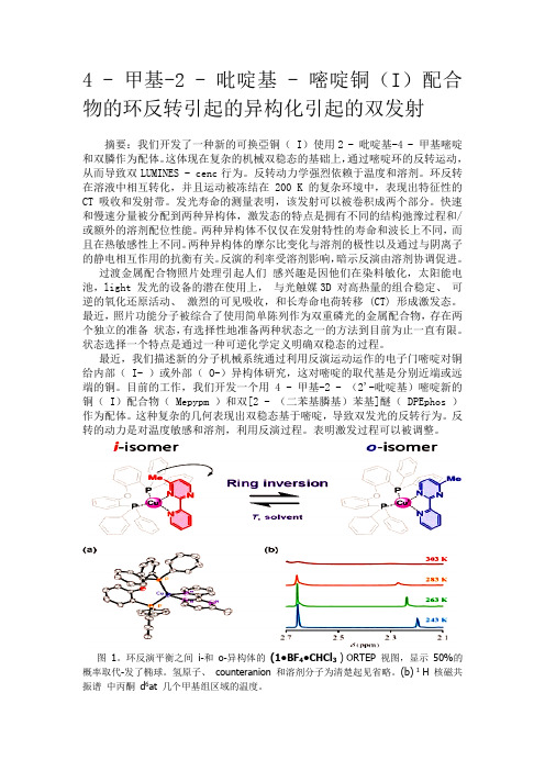
图1。
环反演平衡之间i-和o-异构体的(1•BF4•CHCl3) ORTEP 视图,显示50%的概率取代-发了椭球。
果胶与多酚相互作用机制及其对食品加工特性影响的研究进展

张璇,赵文,高哲,等. 果胶与多酚相互作用机制及其对食品加工特性影响的研究进展[J]. 食品工业科技,2024,45(1):378−386.doi: 10.13386/j.issn1002-0306.2023030201ZHANG Xuan, ZHAO Wen, GAO Zhe, et al. Research Progress on the Interaction Mechanism of Pectin and Polyphenol and Their Effect on Food Processing Characteristics[J]. Science and Technology of Food Industry, 2024, 45(1): 378−386. (in Chinese with English abstract). doi: 10.13386/j.issn1002-0306.2023030201· 专题综述 ·果胶与多酚相互作用机制及其对食品加工特性影响的研究进展张 璇1,赵 文1,2,高 哲1,李美娇1,吴梦颖1,周 茜1,*(1.河北农业大学食品科技学院,河北保定 071000;2.河北省农产品加工工程技术研究中心,河北保定 071000)摘 要:果胶和多酚共存于植物性食品体系中。
除天然存在的果胶-多酚复合物外,在受到加热、高压、干燥等外力作用的食品加工过程中,两者会快速且自发地进行相互作用。
果胶与多酚之间的相互作用会影响食品的理化性质和功能特性。
本文总结了果胶与多酚相互作用的机制、内部和外部多重影响因素、主要的研究方法并结合 Langmuir 和Freundlich 常见的等温吸附模型对果胶与多酚之间的吸附行为进行描述和定量表征。
此外还探讨了两者相互作用对食品加工特性及多酚生物可利用性的影响,分析了该领域的研究方向和发展趋势。
关键词:果胶,多酚,相互作用,等温吸附模型,生物可利用性本文网刊:中图分类号:TS255.1 文献标识码:A 文章编号:1002−0306(2024)01−0378−09DOI: 10.13386/j.issn1002-0306.2023030201Research Progress on the Interaction Mechanism of Pectin and Polyphenol and Their Effect on Food Processing CharacteristicsZHANG Xuan 1,ZHAO Wen 1,2,GAO Zhe 1,LI Meijiao 1,WU Mengying 1,ZHOU Qian 1, *(1.College of Food Science and Technology, Hebei Agricultural University, Baoding 071000, China ;2.Engineering Technology Research Center for Agricultural Product Processing of Hebei, Baoding 071000, China )Abstract :The pectin and polyphenols that co-exist in plant-based food systems form complexes in natural conditions and interact quickly and spontaneously during food processing due to external forces, such as heating, high pressure, and drying.The interaction can affect the physicochemical properties and functional properties of foods. This review summarizes the mechanisms, multiple internal and external influencing factors, and main research methods involved in pectin and polyphenol interaction, while their adsorption behavior is described and quantitatively characterized using the isothermal adsorption model commonly used by Langmuir and Freundlich. In addition, the impact of pectin and polyphenol interaction on food processing characteristics and polyphenol bioavailability is also discussed, and the future research prospects and development trends in this field are analyzed.Key words :pectin ;polyphenol ;interactions ;isothermal adsorption models ;bioavailability果胶是一种酸性杂多糖,广泛存在于蔬菜、水果和谷物等植物细胞壁中,在人类健康中发挥着重要的作用[1]。
合成生物学

谢谢观看
理论背景
理论背景
合成生物学的研究依据自组织系统结构理论 -泛进化论(structurity, structure theory, panevolution theory),从实证到综合(synthetic )探讨天然与人工进化的生物系统理论,阐述了结构整合 (integrative)、调适稳态与建构(constructive)层级等规律;因此,系统(systems)生物学也称为“整 合(integrative biology)生物学”,合成(synthetic)生物学又叫“建构生物学(constructive biology)”(Zeng BJ.中译)。系统与合成生物学的系统结构、发生动力与砖块建构、工程设计等基于结构理 论原理,从电脑技术的系统科学理论到遗传工程的系统科学方法,是将物理科学、工程技术原理与方法贯彻到细 胞、遗传机器与细胞通讯技术等纳米层次的生物分子系统分析与设计。
自2000年《自然》(Nature)杂志报道了人工合成基因线路研究成果以来,合成生物学研究在全世界范围 引起了广泛的**与重视,被公认为在医学、制药、化工、能源、材料、农业等领域都有广阔的应用前景。国际上 的合成生物学研究发展飞速,在短短几年内就已经设计了多种基因控制模块,包括开关、脉冲发生器、振荡器等, 可以有效调节基因表达、蛋白质功能、细胞代谢或细胞间相互作用。
合成生物学(synthetic biology),也可翻译成综合生物学,即综合集成,“synthetic”在不同地方翻 译成不同中文,比如综合哲学(synthetic philosophy)、“社会-心理-生物医学模式”的综合(synthetic) 医学(genbrain biosystem network -中科院曾邦哲1999年建于德国,探讨生物系统分析学“biosystem analysis”与人工生物系统“artificial biosystem”,包括实验、计算、系统、工程研究与应用),同时也 被归属为人工生物系统研究的系统生物工程技术范畴,包括生物反应器与生物计算机开发。
生物传感器
(4)高精度血糖分析仪。高精度血糖分析仪是采用固定化酶的生物传感分析仪。其分精度可以达到 0. 5~2% ,比家用保健类生物传感器几乎高一个数量级,比目前医用生化分析仪的精度也高 2~3个百分点。这在血糖分析领域是非常重要的,它们可以用作血糖分析的标准方法。尤其是在市场销售的手掌型血糖分析仪出现质量事故时,需要另一种有说服力的分析方法证明其分析结果时,固定化酶葡萄糖生物传感分析仪可以作为一种理想的仲裁工具。它们既可作为医用类型的分析仪,还可用作生物技术产业的过程监控、 食品分析、 和科研工具。多种酶传感器研究开发比较成熟,已形成商品。
(2)按照传感器器件检测的原理分类,可分为:热敏生物传感器、 场效应管生物传感器、 压电生物传感器、 光学生物传感器、 声波道生物传感器、酶电极生物传感器、 介体生物传感器等。
(3)按照生物敏感物质相互作用的类型分类,可分为亲和型和代谢型两种。
四、 生物传感器的特点
(1)采用固定化生物活性物质作催化剂,价值昂贵的Байду номын сангаас剂可以重复多次使用,克服了过去酶法分析试剂费用高和化学分析繁琐复杂的缺点。
二、 生物传感器的原理
待测物质经扩散作用进入生物活性材料,经分子识别,发生生物学反应,产生的信息继而被相应的物理或化学换能器转变成可定量和可处理的电信号,再经二次仪表放大并输出,便可知道待测物浓度。
三、 生物传感器的种类
(1)按照其感受器中所采用的生命物质分类,可分为:微生物传感器、免疫传感器、 组织传感器、 细胞传感器、 酶传感器、 DNA传感器等。
可生物降解聚氨酯
可 生 物 降 解 聚 氨 酯张子鹏 顾利霞(中国纺织大学材料学院 上海 200051) 摘 要 本文综述了目前开发的可生物降解聚氨酯的合成及其降解机理,并对可生物降解聚氨酯的发展前景作了评述。
关键词 可生物降解 聚氨酯 降解机理BIODEGRADAB L E POLY URETHANEZhang Z ipeng G u Lixia(China T extile University,Shanghai,200051) Abstract The synthesis and biodegradation mechanism of biodegradable polyurethane are reviewed,and its development prospects are als o discussed in this article.K ey w ords biodegradable polyurethane biodegradation mechanism 聚氨酯(PU)材料是一类性能优异的高分子材料,广泛地应用于交通运输、冶金、建筑、轻工、印刷等工业领域。
到了90年代,聚氨酯越来越多地进入航空、航天、汽车等领域,市场正持续向高峰发展[1]。
预计到2000年,世界聚氨酯年消费量将达到870万t,年均增长率为9%,其中亚太地区年消费平均增长率为10%~20%,超过了世界的的年平均增长率。
而我国是聚氨酯最有潜力、最有希望的市场,年均增长率约为15%[2]。
但是,聚氨酯有不能自然降解的缺点,所以聚氨酯的蓬勃发展也带来了其废弃物污染环境的问题,开发可生物降解聚氨酯材料被认为是解决这一难题的理想途径之一。
1 可生物降解聚氨酯的合成利用聚氨酯的异氰酸酯组分的异氰酸酯基团(-NC O)的高活性和天然高分子化合物的可生物降解性能,把含有多个羟基(-OH)的天然高分子化合物作为聚氨酯多元醇组分之一,制成各种聚氨酯材料,既可以减少多元醇的用量,降低成本,又能赋予制品生物降解性能。
名词委审定 汉英生理学名词
强度-时间曲线 strength-duration curve
顺应 accommodation
适应 adaptation
不应期 refractory period
绝对不应期 absolute refractory period
相对不应期 relative refractory period
最大刺激 maximal stimulus
阈下刺激 subthreshold stimulus
反应 response, reaction
阈下反应 subthreshold response
局部反应 local response
基强度 rheobase
利用时 utilization time
超常期 supranormal period
低常期 subnormal period
极化 polarization
细胞膜两侧电荷不均匀分布的状态。
去极化 depolarization
复极化 repolarization
超极化 hyperpolarization
超射 overshoot
肌电图 electromyogram,EMG
神经生理学 neurophysiology
神经科学 neuroscience
神经生物学 neurobiology
协调 coordination
本能 instinct
组构 organization
整合作用 integration
回荡 reverberation
膜电流 membrane current
膜电阻 membrane resistance
益生素的作用机理及其在饲料中的应用
料添加剂促进动物生长,而且还能明显提高动物
抗病能力,在畜禽饲养中的运用越来越广泛。
21311 反刍动物中的应用 在法国犊牛出生后
立刻投喂健康犊牛的肠道微生物群落,腹泻发病
率由82 %降至35 % ,死亡率由1012 %降至218
%。加拿大研究人员于犊牛出生当日便喂给乳
明的EM微生物制剂,就是由光合细菌、放线菌、
乳酸菌及发酵型丝状真菌5 个科属的多种微生物
复合培养而成的微生物群,具有除粪臭、促生长、
抗病、改善畜禽产品品质等作用。国内四川农业
大学研制的微生态制剂多为芽孢杆菌类。
212 益生素的研制及保藏 在益生素制剂的研
制中,活菌量是衡量产品质量的一个关键指标,但
菌混合物,对鸡进行饲喂试验,结果均对鸡的生长
十分有益。Bibby 公司在0~21 日龄肉仔鸡日粮
中添加益生素,增重提高412 %~619 % ,饲料利
用率提高315 %~415 %。李庆珍报道,用益生
素喂雏鸡比喂抗生素组提高成活率313 %。
[通迅地址:江苏省无锡市惠河路170 号,邮
编:214036 ]
211 菌种的筛选 菌种筛选是益生素研制的关
键。但由于益生素作用机理还不完全清楚,所以
益生素组成菌种的筛选,缺少统一的规范标准。
美国食品与药物管理局曾发表过一张被认为可以
直接饲喂且安全的微生物品种名单,共42 种。日
本的科研工作者在筛选益生素菌种时,并未完全
采用美国的标准。例如日本琉球大学比嘉照夫发
的含菌量应达到108 ~ 109cfu/ g , 或者为106 ~
美国开发出利用生物质生产塑料的新方法
美国开发出利用生物质生产塑料的新方法
佚名
【期刊名称】《国外塑料》
【年(卷),期】2012(000)005
【摘要】美国马萨诸塞州阿默斯特(Amherst)大学和特拉华大学的化学工程师团队已经发现了一种新的方式,利用生物质而不是利用石油来制取塑料瓶。
这是一种高效率、利用可再生资源的方法,用于生产化学品对二甲苯。
这项研究已在美国化学学会杂志"催化(Catalysis)"上发表。
二甲苯化学品被用来制造PET塑料,目前这在许多产品中被使用,
【总页数】1页(P66-66)
【正文语种】中文
【中图分类】TQ517
【相关文献】
1.美科学家发现高收率生产生物质塑料新方法 [J], 金宝珍
2.日本研发出利用糖和细菌合成塑料的新方法 [J], 王兵;
3.荷兰Utrecht大学开发出由生物质生产塑料的催化剂 [J],
4.美国研发出一种高收率生产生物质塑料新方法 [J],
5.日本Yokohama橡胶有限公司研发出世界首例利用生物质生产丁二烯的新技术[J],
因版权原因,仅展示原文概要,查看原文内容请购买。
关于生物名词解释汇总动态部分)
名词解释(动态部分)生物氧化1、底物水平磷酸化(substrate-level phosphorylatio)n : .在底物被氧化的过程中,底物分子内部能量重新分布产生高能磷酸键(或高能硫酯键),由此高能键提供能量使ADP (或GDP )磷酸化生成ATP (或GTP )的过程称为底物水平磷酸化。
此过程与呼吸链的作用无关,以底物水平磷酸化方式只产生少量ATP 。
2、发酵(fermentation)泛指通过微生物的工业培养,利用其新陈代谢实现积累发酵产品的过程,包括有氧和无氧过程3、呼吸链(respiratory chain有机物在生物体内氧化过程中所脱下的氢原子,经过一系列有严格排列顺序的传递体组成的传递体系进行传递,最终与氧结合生成水,这样的电子或氢原子的传递体系称为呼吸链或电子传递链。
电子在逐步的传递过程中释放出能量被用于合成ATP,以作为生物体的能量来源。
4、氧化磷酸化(oxidative phosphorylation)在底物脱氢被氧化时,电子或氢原子在呼吸链上的传递过程中伴随ADP 磷酸化生成ATP 的作用,称为氧化磷酸化。
氧化磷酸化是生物体内的糖、脂肪、蛋白质氧化分解合成ATP 的主要方式。
5、磷氧比P/O(P/O )电子经过呼吸链的传递作用最终与氧结合生成水,在此过程中所释放的能量用于ADP磷酸化生成ATP。
经此过程消耗一个原子的氧所要消耗的无机磷酸的分子数(也是生成ATP的分子数)称为磷氧比值(P/0)。
女口NADH的磷氧比值是3,FADH2 的磷氧比值是2。
糖代谢1、磷酸戊糖途径(pentose phosphate pathway磷酸戊糖途径指机体某些组织(如肝、脂肪组织等)以6-磷酸葡萄糖为起始物在6-磷酸葡萄糖脱氢酶催化下形成6-磷酸葡萄糖酸进而代谢生成磷酸戊糖为中间代谢物的过程,又称为磷酸已糖旁路。
2、糖原异生(gluconeogenesis 非糖物质(如丙酮酸乳酸甘油生糖氨基酸等)转变为葡萄糖的过程。
突触蛋白在学习记忆过程中的作用
突触蛋白在学习记忆过程中的作用
陈菁菁;印大中
【期刊名称】《生命的化学》
【年(卷),期】2006(26)4
【摘要】学习和记忆是脑的高级功能。
学习指人和动物获得外界知识的神经过程;记忆指将获得的知识储存和读出的神经过程。
突触蛋白(synapsin)是一种与突触结构和功能密切相关的膜蛋白,在突触的可塑性以及长时程增强(long-timepotentiation,LTP)中起着重要作用。
而突触可塑性是突触对内外环境变化作出反应的能力,是学习记忆的神经生物学基础。
LTP一直被认为是学习记忆的神经基础之一,是突触可塑性的功能指标,也是研究学习记忆的理想模型。
该文介绍突触蛋白在学习记忆过程中的作用及机制、突触蛋白在学习记忆研究中的应用。
【总页数】3页(P334-336)
【关键词】学习记忆;突触蛋白;突触可塑性;长时程增强
【作者】陈菁菁;印大中
【作者单位】湖南师范大学生命科学学院衰老生化实验室
【正文语种】中文
【中图分类】Q189;Q73
【相关文献】
1.神经肽在学习记忆过程中的作用 [J], 郑元林;吴馥梅
2.PKA-CREB信号通路在大鼠纹状体边缘区及海马空间学习记忆过程中的作用 [J],
常铉;舒斯云;包新民;江刚
3.内源性noggin对学习记忆过程中海马神经发生的调控作用 [J], 范晓棠;徐海伟;罗峻;蔡文琴
4.记忆力在英语学习过程中的作用探究 [J], 杨上杭
5.肉苁蓉多糖对衰老过程中学习记忆影响的体内外作用 [J], 邢海燕;赵璐璐;王胜男;李刚
因版权原因,仅展示原文概要,查看原文内容请购买。
- 1、下载文档前请自行甄别文档内容的完整性,平台不提供额外的编辑、内容补充、找答案等附加服务。
- 2、"仅部分预览"的文档,不可在线预览部分如存在完整性等问题,可反馈申请退款(可完整预览的文档不适用该条件!)。
- 3、如文档侵犯您的权益,请联系客服反馈,我们会尽快为您处理(人工客服工作时间:9:00-18:30)。
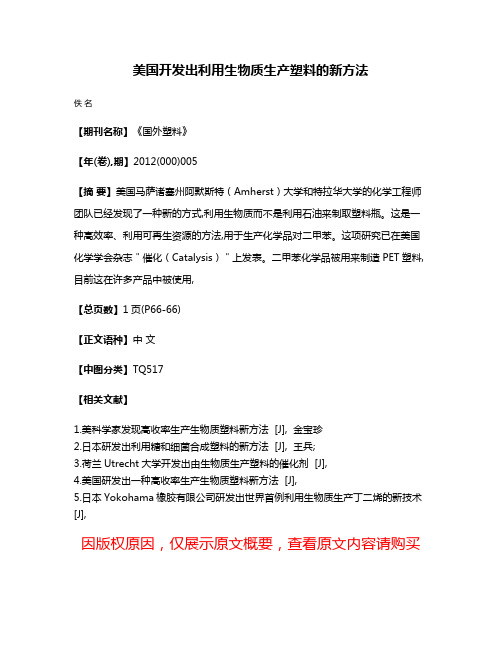
Leading EdgePreviewsSynaptic Plasticity of Feeding Circuits: Hormones and HysteresisMarcelo O.Dietrich1,4and Tamas L.Horvath1,2,3,*1Section of Comparative Medicine2Department of Obstetrics,Gynecology and Reproductive Sciences3Department of NeurobiologyYale University School of Medicine,New Haven,CT06520,USA4Programa de Po´s-graduac¸a˜o em Bioquı´mica,Department of Biochemistry,Universidade Federal do Rio Grande do Sul,Porto Alegre RS90035,Brazil*Correspondence:tamas.horvath@DOI10.1016/j.cell.2011.08.031The drive to eat is controlled by neuronal circuits in the hypothalamus that respond to hormones signaling hunger or satiety.In this issue of Cell,Yang et al.(2011)reveal an AMPK-dependent synaptic pathway that sustains excitatory stimulation of the NPY/AgRP neurons that promote feeding behavior until satiety signals kick in.Metabolic hormones such a ghrelin,sig-naling food deprivation,and leptin,sig-naling satiety,stimulate synaptic activity and plasticity within the neuronal circuits in the hypothalamus that control feeding behavior(Pinto et al.,2004).This process was suggested to play an important role in regulating metabolism(Horvath and Diano,2004).However,the mechanisms that bring about these rapid changes in synaptic connectivity and activity and how long they persist remain ill defined. In this issue of Cell,Yang et al.(2011) provide a remarkable set of novelfindings pinpointing intracellular and intercellular substrates of synaptic plasticity on the orexigenic NPY/AgRP neurons.Their findings demonstrate why the response to a pulse of the appetite-stimulating hor-mone ghrelin can persist for hours,and how it can be turned off in response to a pulse of ing in vitro electro-physiological approaches to record from neurons marked by the expression of the neuropeptide NPY,most of which also synthesize the neuropeptide AgRP,the authors found that food deprivation in-creases the frequency of action potentials in the these neurons(referred to as AgRP neurons by Yang et al.).The increased activity occurs through an AMPA-medi-ated increase in frequency of miniature excitatory postsynaptic currents(mEPSCs) onto these cells.This increase in excitatory inputs is driven by AMPK-and ryanodine re-ceptor-mediated calcium release frominternal stores in presynaptic sites.Ad-ministration of ghrelin mimicked theeffect of food deprivation on mEPSCs inin vitro experiments,consistent withghrelin’s previously identified action onmidbrain dopamine neurons(Abizaidet al.,2006).The authors demonstratethat calcium/calmodulin-dependent pro-tein kinase kinase(CAMKK)activatesAMPK in response to ghrelin to unleashsynaptic activity that exhibits hysteresis,i.e.,it can persist for hours.The hyster-etic nature of this signaling is likely dueto the positive feedback loop betweencalcium release triggered by AMPKactivity,which in turn leads to additionalAMPK activity promoted by CAMKK.The enhanced synaptic transmissionwas switched off by the appetite-sup-pressing hormone leptin,which activatesthe pro-opiomelanocortin(POMC)neu-rons.Intriguingly,the authors show thatopiods derived from these neurons,most likely b-endorphin,reverse theAMPK-mediated upregulation of excit-atory inputs onto AgRP neurons(Fig-ure1A).Thefindings thus provide a puta-tive physiological explanation for whymammals no longer feel the drive to eatonce satiety is reached.Changes in synaptic transmission oc-cur within a very short period of time inresponse to the changing metabolic envi-ronment.One of the ingenious aspects ofthe work of Yang et al.is that the authorsrecognized that such a physiologicalphenomenon is virtually impossible tothoroughly investigate with any availabletransgenic or knockout technology.Thus,the authors used elegantly appliedpharmacological tools to test and answer,in a manner not previously attempted,fundamental questions about synaptictransmission governed by metabolicsignals.Conceptually,the work of Yang et al.(2011)builds on previous reports thathave proposed mechanisms related toAgRP neuronal plasticity,but the authorsexcel in providing a refined and unifyingframework for synaptic regulation,main-tenance,and resetting by metabolic al-terations.The AgRP neurons have beenconsidered the primary responders togut-derived metabolic hormones such asghrelin.This notion is left in the dust bythe study of Yang et al.,whosefindingspoint to an AMPK-dependent presynapticmechanism that kicks off adaptationto ghrelin.This presynaptic mechanismlikely acts in synergy with autonomouscell adaptations that occur within theAgRP neurons,allowing them to increasefiring rate in a sustained way in responseto food deprivation(Takahashi andCone,2005)or ghrelin(Kohno et al.,2008)in the absence of synaptic inputs.This cell-autonomous mechanism is alsodependent upon AMPK,as well as ondownstream mitochondrial factors andSirtuin1activation in AgRP neuronsCell146,September16,2011ª2011Elsevier Inc.863(Andrews et al.,2008;Kohno et al.,2008;Dietrich et al.,2010)(Figure 1B).Yang et al.did not identify the presyn-aptic cells that undergo AMPK-depen-dent calcium release to stimulate AgRP neurons.The presynaptic nature of the effect was concluded based in part upon comparing the effects of AMPK inhibitors when permitted to affect all cells versus when restricted to AgRP neurons by direct intracellular delivery.Thus the iden-tities of the cells that are mediating the responses to food deprivation and ghrelin remain in question.The data presented by Yang et al.indicate that presynaptic boutons in direct contact with the AgRP neurons might be the site where the intra-cellular events involving AMPK,calcium mobilization,and opioid action take place to affect release probabilities.This is a very reasonable assumption,and the cells of origin of these terminals will be of interest to pursue.However,other mech-anisms may also be in place in support of this process.For example,astrocytes that surround glutamatergic synapses could also contain the AMPK-dependent machinery to modulate synaptic plasticity and neurotransmitter release probability by regulating the synaptic bioenergetics and/or neurotransmitter uptake (Fig-ure 1B).Alternatively,in line with the conclusions of the current study,the opioid factor released by the POMC neurons could diffuse into the arcuate nucleus,a cluster of hypothalamic neu-rons that are involved in neuroendocrine responses,resulting in local modulatory activity.In addition,although the current report focused on the role of the excit-atory projections onto the AgRP neurons,it is also possible that inhibitory synapses may be involved in regulating AgRP neu-ronal excitability.Finally,it is worth noting that the exper-iments performed by Yang et al.were in vitro recordings.In such settings,the milieu is different from physiological situa-tions in which AgRP neurons are active.For example,the media used for record-ings contained an 11mM concentration of glucose.This level of glucose is at least a magnitude above that which occurs during a food-deprived state,and it is substantially higher than that of the fed state.Lower,more physiological levels of glucose in such in vitro conditions were shown to have differential effects on AgRP neurons depending on postsyn-aptic AMPK content (Claret et al.,2007).Additionally,the effect of the AMPK activator AICAR (used by Yang and colleagues as well)on feeding behavior was blunted in mice lacking mitochondrial uncoupling protein 2(Andrews et al.,2008),suggesting that AMPK’s role in hypothalamic circuit regulation may be more complex.In summary,the tour-de-force study by Yang et al.highlights a fundamentally novel mechanism that depicts regulatory principles of hypothalamic AgRP neurons in a paradigm-shifting manner.The paper indicates that the current dogma that AgRP neurons represent the first-order neurons in brain sensing peripheral meta-bolic status may need to be revised.REFERENCESAbizaid,A.,Liu,Z.-W.,Andrews,Z.B.,Shanab-rough,M.,Borok,E.,Elsworth,J.D.,Roth,R.H.,Sleeman,M.W.,Picciotto,M.R.,Tscho¨p,M.H.,et al.(2006).J.Clin.Invest.116,3229–3239.Andrews,Z.B.,Liu,Z.W.,Walllingford,N.,Erion,D.M.,Borok,E.,Friedman,J.M.,Tscho¨p,M.H.,Shanabrough,M.,Cline,G.,Shulman,G.I.,et al.(2008).Nature 454,846–851.Claret,M.,Smith,M.A.,Batterham,R.L.,Selman,C.,Choudhury,A.I.,Fryer,L.G.D.,Clements,M.,Figure 1.AgRP Neurons Respond to Changing Metabolic States(A)In response to food deprivation and the ghrelin hormone,a presynaptic pathway involving a positive feedback loop of AMPK-mediated calcium release stimulates the activity of AgRP neurons.The activity of these neurons is known to drive feeding behavior.The hormone leptin signals satiety and induces the POMC neurons to release opioids that turn off the AMPK pathway and,consequently,AgRP neuronal activity.POMC neurons are also known to have an inhibitory synaptic connection with AgRP neurons mediated by GABA,NPY,and/or AgRP.(B)Under in vivo conditions,a combination of mechanisms likely contributes to the regulation of AgRP neuronal activity.In addition to the presynaptic signaling pathway uncovered by Yang et al.,there may be postsynaptic and cell-autonomous intracellular signaling cascades.In addition,the AMPK-dependent presynaptic mechanism could also be located in other cell types,such as the POMC neurons and astrocytes (yellow).Ghrsr1is the ghrelin receptor.864Cell 146,September 16,2011ª2011Elsevier Inc.Al-Qassab,H.,Heffron,H.,Xu,A.W.,et al.(2007). J.Clin.Invest.117,2325–2336.Dietrich,M.O.,Antunes,C.,Geliang,G.,Liu,Z.W., Borok,E.,Nie,Y.,Xu,A.W.,Souza,D.O.,Gao,Q., Diano,S.,et al.(2010).J.Neurosci.30,11815–11825.Horvath,T.L.,and Diano,S.(2004).Nat.Rev.Neurosci.5,662–667.Kohno,D.,Sone,H.,Minokoshi,Y.,and Yada,T.(2008)mun.366,388–392.Pinto,S.,Roseberry, A.G.,Liu,H.,Diano,S.,Shanabrough,M.,Cai,X.,Friedman,J.M.,andHorvath,T.L.(2004).Science304,110–115.Takahashi,K.A.,and Cone,R.D.(2005).Endocri-nology146,1043–1047.Yang,Y.,Atasoy,D.,Su,H.H.,and Sternson,S.M.(2011).Cell146,this issue,992–1003.Cell146,September16,2011ª2011Elsevier Inc.865。