Ultrathin epitaxial graphite 2D electron gas properties and a route toward graphene-based n
石墨烯的制备及其在铅酸电池中的应用
石墨烯的制备及其在铅酸电池中的应用石沫;杨新新;周明明;吴亮;柯娃;李厚训;戴贵平【摘要】添加炭材料能够明显地提高铅酸电池的性能。
石墨烯是具有独特平面二维结构的炭材料,具有很多优异的性能,如良好的导电性和很高的比表面积。
本文综述了石墨烯的制备方法,并对目前石墨烯在铅酸电池中的应用情况进行了研究和总结。
%Carbon materials can significantly improve the performance of lead-acid batteries. Graphene is a kind of carbon materials with unique two-dimensional structure, which has a lot of excellent performance, such as good electrical conductivity and high speciifc surface area. This paper reviews the preparation methods of graphene, and its application in lead-acid batteries.【期刊名称】《蓄电池》【年(卷),期】2015(000)003【总页数】4页(P142-145)【关键词】炭材料;石墨烯;导电性;铅酸电池【作者】石沫;杨新新;周明明;吴亮;柯娃;李厚训;戴贵平【作者单位】超威电源有限公司研究院,浙江湖州313100;超威电源有限公司研究院,浙江湖州313100;超威电源有限公司研究院,浙江湖州313100;超威电源有限公司研究院,浙江湖州313100;超威电源有限公司研究院,浙江湖州313100;超威电源有限公司研究院,浙江湖州313100;超威电源有限公司研究院,浙江湖州313100【正文语种】中文【中图分类】TM912.1石墨烯是碳原子紧密堆积的二维蜂窝状晶格结构的碳质材料,碳原子排列呈平面六边形结构,在二维平面上每个碳原子以 sp2杂化轨道相连接[1]。
半导体制造技术
Semiconductor Manufacturing Technology半导体制造技术Instructor’s ManualMichael QuirkJulian SerdaCopyright Prentice HallTable of Contents目录OverviewI. Chapter1. Semiconductor industry overview2. Semiconductor materials3. Device technologies—IC families4. Silicon and wafer preparation5. Chemicals in the industry6. Contamination control7. Process metrology8. Process gas controls9. IC fabrication overview10. Oxidation11. Deposition12. Metallization13. Photoresist14. Exposure15. Develop16. Etch17. Ion implant18. Polish19. Test20. Assembly and packagingII. Answers to End-of-Chapter Review QuestionsIII. Test Bank (supplied on diskette)IV. Chapter illustrations, tables, bulleted lists and major topics (supplied on CD-ROM)Notes to Instructors:1)The chapter overview provides a concise summary of the main topics in each chapter.2)The correct answer for each test bank question is highlighted in bold. Test bankquestions are based on the end-of-chapter questions. If a student studies the end-of-chapter questions (which are linked to the italicized words in each chapter), then they will be successful on the test bank questions.2Chapter 1Introduction to the Semiconductor Industry Die:管芯 defective:有缺陷的Development of an Industry•The roots of the electronic industry are based on the vacuum tube and early use of silicon for signal transmission prior to World War II. The first electronic computer, the ENIAC, wasdeveloped at the University of Pennsylvania during World War II.•William Shockley, John Bardeen and Walter Brattain invented the solid-state transistor at Bell Telephone Laboratories on December 16, 1947. The semiconductor industry grew rapidly in the 1950s to commercialize the new transistor technology, with many early pioneers working inSilicon Valley in Northern California.Circuit Integration•The first integrated circuit, or IC, was independently co-invented by Jack Kilby at Texas Instruments and Robert Noyce at Fairchild Semiconductor in 1959. An IC integrates multiple electronic components on one substrate of silicon.•Circuit integration eras are: small scale integration (SSI) with 2 - 50 components, medium scale integration (MSI) with 50 – 5k components, large scale integration (LSI) with 5k to 100kcomponents, very large scale integration (VLSI) with 100k to 1M components, and ultra large scale integration (ULSI) with > 1M components.1IC Fabrication•Chips (or die) are fabricated on a thin slice of silicon, known as a wafer (or substrate). Wafers are fabricated in a facility known as a wafer fab, or simply fab.•The five stages of IC fabrication are:Wafer preparation: silicon is purified and prepared into wafers.Wafer fabrication: microchips are fabricated in a wafer fab by either a merchant chip supplier, captive chip producer, fabless company or foundry.Wafer test: Each individual die is probed and electrically tested to sort for good or bad chips.Assembly and packaging: Each individual die is assembled into its electronic package.Final test: Each packaged IC undergoes final electrical test.•Key semiconductor trends are:Increase in chip performance through reduced critical dimensions (CD), more components per chip (Moore’s law, which predicts the doubling of components every 18-24 months) andreduced power consumption.Increase in chip reliability during usage.Reduction in chip price, with an estimated price reduction of 100 million times for the 50 years prior to 1996.The Electronic Era•The 1950s saw the development of many different types of transistor technology, and lead to the development of the silicon age.•The 1960s were an era of process development to begin the integration of ICs, with many new chip-manufacturing companies.•The 1970s were the era of medium-scale integration and saw increased competition in the industry, the development of the microprocessor and the development of equipment technology. •The 1980s introduced automation into the wafer fab and improvements in manufacturing efficiency and product quality.•The 1990s were the ULSI integration era with the volume production of a wide range of ICs with sub-micron geometries.Career paths•There are a wide range of career paths in semiconductor manufacturing, including technician, engineer and management.2Chapter 2 Characteristics of Semiconductor MaterialsAtomic Structure•The atomic model has three types of particles: neutral neutrons(不带电的中子), positively charged protons(带正电的质子)in the nucleus and negatively charged electrons(带负电的核外电子) that orbit the nucleus. Outermost electrons are in the valence shell, and influence the chemical and physical properties of the atom. Ions form when an atom gains or loses one or more electrons.The Periodic Table•The periodic table lists all known elements. The group number of the periodic table represents the number of valence shell electrons of the element. We are primarily concerned with group numbers IA through VIIIA.•Ionic bonds are formed when valence shell electrons are transferred from the atoms of one element to another. Unstable atoms (e.g., group VIIIA atoms because they lack one electron) easily form ionic bonds.•Covalent bonds have atoms of different elements that share valence shell electrons.3Classifying Materials•There are three difference classes of materials:ConductorsInsulatorsSemiconductors•Conductor materials have low resistance to current flow, such as copper. Insulators have high resistance to current flow. Capacitance is the storage of electrical charge on two conductive plates separated by a dielectric material. The quality of the insulation material between the plates is the dielectric constant. Semiconductor materials can function as either a conductor or insulator.Silicon•Silicon is an elemental semiconductor material because of four valence shell electrons. It occurs in nature as silica and is refined and purified to make wafers.•Pure silicon is intrinsic silicon. The silicon atoms bond together in covalent bonds, which defines many of silicon’s properties. Silicon atoms bond together in set, repeatable patterns, referred to asa crystal.•Germanium was the first semiconductor material used to make chips, but it was soon replaced by silicon. The reasons for this change are:Abundance of siliconHigher melting temperature for wider processing rangeWide temperature range during semiconductor usageNatural growth of silicon dioxide•Silicon dioxide (SiO2) is a high quality, stable electrical insulator material that also serves as a good chemical barrier to protect silicon from external contaminants. The ability to grow stable, thin SiO2 is fundamental to the fabrication of Metal-Oxide-Semiconductor (MOS) devices. •Doping increases silicon conductivity by adding small amounts of other elements. Common dopant elements are from trivalent, p-type Group IIIA (boron) and pentavalent, n-type Group VA (phosphorus, arsenic and antimony).•It is the junction between the n-type and p-type doped regions (referred to as a pn junction) that permit silicon to function as a semiconductor.4Alternative Semiconductor Materials•The alternative semiconductor materials are primarily the compound semiconductors. They are formed from Group IIIA and Group VA (referred to as III-V compounds). An example is gallium arsenide (GaAs).•Some alternative semiconductors come from Group IIA and VIA, referred to as II-VI compounds. •GaAs is the most common III-V compound semiconductor material. GaAs ICs have greater electron mobility, and therefore are faster than ICs made with silicon. GaAs ICs also have higher radiation hardness than silicon, which is better for space and military applications. The primary disadvantage of GaAs is the lack of a natural oxide.5Chapter 3Device TechnologiesCircuit Types•There are two basic types of circuits: analog and digital. Analog circuits have electrical data that varies continuously over a range of voltage, current and power values. Digital circuits have operating signals that vary about two distinct voltage levels – a high and a low.Passive Component Structures•Passive components such as resistors and capacitors conduct electrical current regardless of how the component is connected. IC resistors are a passive component. They can have unwanted resistance known as parasitic resistance. IC capacitor structures can also have unintentional capacitanceActive Component Structures•Active components, such as diodes and transistors can be used to control the direction of current flow. PN junction diodes are formed when there is a region of n-type semiconductor adjacent to a region of p-type semiconductor. A difference in charge at the pn junction creates a depletion region that results in a barrier voltage that must be overcome before a diode can be operated. A bias voltage can be configured to have a reverse bias, with little or no conduction through the diode, or with a forward bias, which permits current flow.•The bipolar junction transistor (BJT) has three electrodes and two pn junctions. A BJT is configured as an npn or pnp transistor and biased for conduction mode. It is a current-amplifying device.6• A schottky diode is formed when metal is brought in contact with a lightly doped n-type semiconductor material. This diode is used in faster and more power efficient BJT circuits.•The field-effect transistor (FET), a voltage-amplifying device, is more compact and power efficient than BJT devices. A thin gate oxide located between the other two electrodes of the transistor insulates the gate on the MOSFET. There are two categories of MOSFETs, nMOS (n-channel) and pMOS (p-channel), each which is defined by its majority current carriers. There is a biasing scheme for operating each type of MOSFET in conduction mode.•For many years, nMOS transistors have been the choice of most IC manufacturers. CMOS, with both nMOS and pMOS transistors in the same IC, has been the most popular device technology since the early 1980s.•BiCMOS technology makes use of the best features of both CMOS and bipolar technology in the same IC device.•Another way to categorize FETs is in terms of enhancement mode and depletion mode. The major different is in the way the channels are doped: enhancement-mode channels are doped opposite in polarity to the source and drain regions, whereas depletion mode channels are doped the same as their respective source and drain regions.Latchup in CMOS Devices•Parasitic transistors can create a latchup condition(???????) in CMOS ICs that causes transistors to unintentionally(无心的) turn on. To control latchup, an epitaxial layer is grown on the wafer surface and an isolation barrier(隔离阻障)is placed between the transistors. An isolation layer can also be buried deep below the transistors.Integrated Circuit Productsz There are a wide range of semiconductor ICs found in electrical and electronic products. This includes the linear IC family, which operates primarily with anal3og circuit applications, and the digital IC family, which includes devices that operate with binary bits of data signals.7Chapter 4Silicon and Wafer Preparation8z Semiconductor-Grade Silicon•The highly refined silicon used for wafer fabrication is termed semiconductor-grade silicon (SGS), and sometimes referred to as electronic-grade silicon. The ultra-high purity of semiconductor-grade silicon is obtained from a multi-step process referred to as the Siemens process.Crystal Structure• A crystal is a solid material with an ordered, 3-dimensional pattern over a long range. This is different from an amorphous material that lacks a repetitive structure.•The unit cell is the most fundamental entity for the long-range order found in crystals. The silicon unit cell is a face-centered cubic diamond structure. Unit cells can be organized in a non-regular arrangement, known as a polycrystal. A monocrystal are neatly arranged unit cells.Crystal Orientation•The orientation of unit cells in a crystal is described by a set of numbers known as Miller indices.The most common crystal planes on a wafer are (100), (110), and (111). Wafers with a (100) crystal plane orientation are most common for MOS devices, whereas (111) is most common for bipolar devices.Monocrystal Silicon Growth•Silicon monocrystal ingots are grown with the Czochralski (CZ) method to achieve the correct crystal orientation and doping. A CZ crystal puller is used to grow the silicon ingots. Chunks of silicon are heated in a crucible in the furnace of the puller, while a perfect silicon crystal seed is used to start the new crystal structure.• A pull process serves to precisely replicate the seed structure. The main parameters during the ingot growth are pull rate and crystal rotation. More homogeneous crystals are achieved with a magnetic field around the silicon melt, known as magnetic CZ.•Dopant material is added to the melt to dope the silicon ingot to the desired electrical resistivity.Impurities are controlled during ingot growth. A float-zone crystal growth method is used toachieve high-purity silicon with lower oxygen content.•Large-diameter ingots are grown today, with a transition underway to produce 300-mm ingot diameters. There are cost benefits for larger diameter wafers, including more die produced on a single wafer.Crystal Defects in Silicon•Crystal defects are interruptions in the repetitive nature of the unit cell. Defect density is the number of defects per square centimeter of wafer surface.•Three general types of crystal defects are: 1) point defects, 2) dislocations, and 3) gross defects.Point defects are vacancies (or voids), interstitial (an atom located in a void) and Frenkel defects, where an atom leaves its lattice site and positions itself in a void. A form of dislocation is astacking fault, which is due to layer stacking errors. Oxygen-induced stacking faults are induced following thermal oxidation. Gross defects are related to the crystal structure (often occurring during crystal growth).Wafer Preparation•The cylindrical, single-crystal ingot undergoes a series of process steps to create wafers, including machining operations, chemical operations, surface polishing and quality checks.•The first wafer preparation steps are the shaping operations: end removal, diameter grinding, and wafer flat or notch. Once these are complete, the ingot undergoes wafer slicing, followed by wafer lapping to remove mechanical damage and an edge contour. Wafer etching is done to chemically remove damage and contamination, followed by polishing. The final steps are cleaning, wafer evaluation and packaging.Quality Measures•Wafer suppliers must produce wafers to stringent quality requirements, including: Physical dimensions: actual dimensions of the wafer (e.g., thickness, etc.).Flatness: linear thickness variation across the wafer.Microroughness: peaks and valleys found on the wafer surface.Oxygen content: excessive oxygen can affect mechanical and electrical properties.Crystal defects: must be minimized for optimum wafer quality.Particles: controlled to minimize yield loss during wafer fabrication.Bulk resistivity(电阻系数): uniform resistivity from doping during crystal growth is critical. Epitaxial Layer•An epitaxial layer (or epi layer) is grown on the wafer surface to achieve the same single crystal structure of the wafer with control over doping type of the epi layer. Epitaxy minimizes latch-up problems as device geometries continue to shrink.Chapter 5Chemicals in Semiconductor FabricationEquipment Service Chase Production BayChemical Supply Room Chemical Distribution Center Holding tank Chemical drumsProcess equipmentControl unit Pump Filter Raised and perforated floorElectronic control cablesSupply air ductDual-wall piping for leak confinement PumpFilterChemical control and leak detection Valve boxes for leak containment Exhaust air ductStates of Matter• Matter in the universe exists in 3 basic states (宇宙万物存在着三种基本形态): solid, liquid andgas. A fourth state is plasma.Properties of Materials• Material properties are the physical and chemical characteristics that describe its unique identity.• Different properties for chemicals in semiconductor manufacturing are: temperature, pressure andvacuum, condensation, vapor pressure, sublimation and deposition, density, surface tension, thermal expansion and stress.Temperature is a measure of how hot or cold a substance is relative to another substance. Pressure is the force exerted per unit area. Vacuum is the removal of gas molecules.Condensation is the process of changing a gas into a liquid. Vaporization is changing a liquidinto a gas.Vapor pressure is the pressure exerted by a vapor in a closed container at equilibrium.Sublimation is the process of changing a solid directly into a gas. Deposition is changing a gas into a solid.Density is the mass of a substance divided by its volume.Surface tension of a liquid is the energy required to increase the surface area of contact.Thermal expansion is the increase in an object’s dimension due to heating.Stress occurs when an object is exposed to a force.Process Chemicals•Semiconductor manufacturing requires extensive chemicals.• A chemical solution is a chemical mixture. The solvent is the component of the solution present in larger amount. The dissolved substances are the solutes.•Acids are solutions that contain hydrogen and dissociate in water to yield hydronium ions. A base is a substance that contains the OH chemical group and dissociates in water to yield the hydroxide ion, OH-.•The pH scale is used to assess the strength of a solution as an acid or base. The pH scale varies from 0 to 14, with 7 being the neutral point. Acids have pH below 7 and bases have pH values above 7.• A solvent is a substance capable of dissolving another substance to form a solution.• A bulk chemical distribution (BCD) system is often used to deliver liquid chemicals to the process tools. Some chemicals are not suitable for BCD and instead use point-of-use (POU) delivery, which means they are stored and used at the process station.•Gases are generally categorized as bulk gases or specialty gases. Bulk gases are the relatively simple gases to manufacture and are traditionally oxygen, nitrogen, hydrogen, helium and argon.The specialty gases, or process gases, are other important gases used in a wafer fab, and usually supplied in low volume.•Specialty gases are usually transported to the fab in metal cylinders.•The local gas distribution system requires a gas purge to flush out undesirable residual gas. Gas delivery systems have special piping and connections systems. A gas stick controls the incoming gas at the process tool.•Specialty gases may be classified as hydrides, fluorinated compounds or acid gases.Chapter 6Contamination Control in Wafer FabsIntroduction•Modern semiconductor manufacturing is performed in a cleanroom, isolated from the outside environment and contaminants.Types of contamination•Cleanroom contamination has five categories: particles, metallic impurities, organic contamination, native oxides and electrostatic discharge. Killer defects are those causes of failure where the chip fails during electrical test.Particles: objects that adhere to a wafer surface and cause yield loss. A particle is a killer defect if it is greater than one-half the minimum device feature size.Metallic impurities: the alkali metals found in common chemicals. Metallic ions are highly mobile and referred to as mobile ionic contaminants (MICs).Organic contamination: contains carbon, such as lubricants and bacteria.Native oxides: thin layer of oxide growth on the wafer surface due to exposure to air.Electrostatic discharge (ESD): uncontrolled transfer of static charge that can damage the microchip.Sources and Control of Contamination•The sources of contamination in a wafer fab are: air, humans, facility, water, process chemicals, process gases and production equipment.Air: class number designates the air quality inside a cleanroom by defining the particle size and density.Humans: a human is a particle generator. Humans wear a cleanroom garment and follow cleanroom protocol to minimize contamination.Facility: the layout is generally done as a ballroom (open space) or bay and chase design.Laminar airflow with air filtering is used to minimize particles. Electrostatic discharge iscontrolled by static-dissipative materials, grounding and air ionization.Ultrapure deiniozed (DI) water: Unacceptable contaminants are removed from DI water through filtration to maintain a resistivity of 18 megohm-cm. The zeta potential represents a charge on fine particles in water, which are trapped by a special filter. UV lamps are used for bacterial sterilization.Process chemicals: filtered to be free of contamination, either by particle filtration, microfiltration (membrane filter), ultrafiltration and reverse osmosis (or hyperfiltration).Process gases: filtered to achieve ultraclean gas.Production equipment: a significant source of particles in a fab.Workstation design: a common layout is bulkhead equipment, where the major equipment is located behind the production bay in the service chase. Wafer handling is done with robotic wafer handlers. A minienvironment is a localized environment where wafers are transferred on a pod and isolated from contamination.Wafer Wet Cleaning•The predominant wafer surface cleaning process is with wet chemistry. The industry standard wet-clean process is the RCA clean, consisting of standard clean 1 (SC-1) and standard clean 2 (SC-2).•SC-1 is a mixture of ammonium hydroxide, hydrogen peroxide and DI water and capable of removing particles and organic materials. For particles, removal is primarily through oxidation of the particle or electric repulsion.•SC-2 is a mixture of hydrochloric acid, hydrogen peroxide and DI water and used to remove metals from the wafer surface.•RCA clean has been modified with diluted cleaning chemistries. The piranha cleaning mixture combines sulfuric acid and hydrogen peroxide to remove organic and metallic impurities. Many cleaning steps include an HF last step to remove native oxide.•Megasonics(兆声清洗) is widely used for wet cleaning. It has ultrasonic energy with frequencies near 1 MHz. Spray cleaning will spray wet-cleaning chemicals onto the wafer. Scrubbing is an effective method for removing particles from the wafer surface.•Wafer rinse is done with overflow rinse, dump rinse and spray rinse. Wafer drying is done with spin dryer or IPA(异丙醇) vapor dry (isopropyl alcohol).•Some alternatives to RCA clean are dry cleaning, such as with plasma-based cleaning, ozone and cryogenic aerosol cleaning.Chapter 7Metrology and Defect InspectionIC Metrology•In a wafer fab, metrology refers to the techniques and procedures for determining physical and electrical properties of the wafer.•In-process data has traditionally been collected on monitor wafers. Measurement equipment is either stand-alone or integrated.•Yield is the percent of good parts produced out of the total group of parts started. It is an indicator of the health of the fabrication process.Quality Measures•Semiconductor quality measures define the requirements for specific aspects of wafer fabrication to ensure acceptable device performance.•Film thickness is generally divided into the measurement of opaque film or transparent film. Sheet resistance measured with a four-point probe is a common method of measuring opaque films (e.g., metal film). A contour map shows sheet resistance deviations across the wafer surface.•Ellipsometry is a nondestructive, noncontact measurement technique for transparent films. It works based on linearly polarized light that reflects off the sample and is elliptically polarized.•Reflectometry is used to measure a film thickness based on how light reflects off the top and bottom surface of the film layer. X-ray and photoacoustic technology are also used to measure film thickness.•Film stress is measured by analyzing changes in the radius of curvature of the wafer. Variations in the refractive index are used to highlight contamination in the film.•Dopant concentration is traditionally measured with a four-point probe. The latest technology is the thermal-wave system, which measures the lattice damage in the implanted wafer after ion implantation. Another method for measuring dopant concentration is spreading resistance probe. •Brightfield detection is the traditional light source for microscope equipment. An optical microscope uses light reflection to detect surface defects. Darkfield detection examines light scattered off defects on the wafer surface. Light scattering uses darkfield detection to detectsurface particles by illuminating the surface with laser light and then using optical imaging.•Critical dimensions (CDs) are measured to achieve precise control over feature size dimensions.The scanning electron microscope is often used to measure CDs.•Conformal step coverage is measured with a surface profiler that has a stylus tip.•Overlay registration measures the ability to accurately print photoresist patterns over a previously etched pattern.•Capacitance-voltage (C-V) test is used to verify acceptable charge conditions and cleanliness at the gate structure in a MOS device.Analytical Equipment•The secondary-ion mass spectrometry (SIMS) is a method of eroding a wafer surface with accelerated ions in a magnetic field to analyze the surface material composition.•The atomic force microscope (AFM) is a surface profiler that scans a small, counterbalanced tip probe over the wafer to create a 3-D surface map.•Auger electron spectroscopy (AES) measures composition on the wafer surface by measuring the energy of the auger electrons. It identifies elements to a depth of about 2 nm. Another instrument used to identify surface chemical species is X-ray photoelectron spectroscopy (XPS).•Transmission electron microscopy (TEM) uses a beam of electrons that is transmitted through a thin slice of the wafer. It is capable of quantifying very small features on a wafer, such as silicon crystal point defects.•Energy-dispersive spectrometer (EDX) is a widely used X-ray detection method for identifying elements. It is often used in conjunction with the SEM.• A focused ion beam (FIB) system is a destructive technique that focuses a beam of ions on the wafer to carve a thin cross section from any wafer area. This permits analysis of the wafermaterial.Chapter 8Gas Control in Process ChambersEtch process chambers••The process chamber is a controlled vacuum environment where intended chemical reactions take place under controlled conditions. Process chambers are often configured as a cluster tool. Vacuum•Vacuum ranges are low (rough) vacuum, medium vacuum, high vacuum and ultrahigh vacuum (UHV). When pressure is lowered in a vacuum, the mean free path(平均自由行程) increases, which is important for how gases flow through the system and for creating a plasma.Vacuum Pumps•Roughing pumps are used to achieve a low to medium vacuum and to exhaust a high vacuum pump. High vacuum pumps achieve a high to ultrahigh vacuum.•Roughing pumps are dry mechanical pumps or a blower pump (also referred to as a booster). Two common high vacuum pumps are a turbomolecular (turbo) pump and cryopump. The turbo pump is a reliable, clean pump that works on the principle of mechanical compression. The cryopump isa capture pump that removes gases from the process chamber by freezing them.。
我国揭示锯齿形边缘石墨烯纳米带中的电声子耦合效应
^ A
l、 _ _
2 1 年 第 8 第6 ( 第 4 期 ) 0 1 )
_
-
A
_ ’ 。-
…
l ≤l
{
(o) V c和光 电转 换 效率(1相 比前者 分 别提 高 了 r )
96 .%和4 . 42 %,表 面 钝 化使 得 短 波长 和 长 波 长 光 的 响 应 明 显 提 高 。为 了使A , 化 效 果 充 I 钝 O
离 子 刻 蚀 技 术 , 首 次 实 现 了可 控 的石 墨烯 面 内各 向异 性 刻 蚀 技 术 ; 并 结 合 人 工 缺 陷 工 程 ,首 次 实现 了对 石 墨 烯 纳 米 结构 的精 确 加 工 和 剪 裁 ,制 备 出 了尺 寸 可 控 ( 小 线 宽达 最 5 米 以下 )、边 缘 可 控 ( 有 原 子级 平 整 的 纳 具 锯 齿 形边 缘 结构 )的石 墨烯 纳米 结构 。 最近 ,张广 宇研 究组 的杨 蓉博 士等在 先前 的 工 作 基 础 上 ,利 用 拉 曼 散 射 光 谱 技 术 ,研 究 了具 有 锯 齿 形 边 缘 结 构 的石 墨 烯 纳 米 带 的 电声 子 耦 合 特 性 。他 们 首 次 在 这 种 结构 中观 察 到 了G 的 劈裂 ( 一1 8 软化 的E g 式 ; 峰 G 53 2模 G+ 1 9 本 征 的E g 式 ) 。这 种 非 应 力 效 应 一5 4 2模 导致 的G 劈 裂可 归因于 锯 齿 形边 缘 结构 独特 峰
1 扁置 场 。
’ ■ 《 I ●
纳 米 尺 度 的Al 膜 ,并 在 一 定 的气 氛和 温 ,薄 O
度 下 进 行激 活 处 理 ,形 成 良好 的 复合 钝 化 薄 膜 结构 。 系 统 实验 表 明 ,不 使 用A , 使 用 1 和 O A , 电池 差 别 十 分 明 显 , 后 者 的 开 路 电 压 l 的 O
基于锐钛矿型TiO2纳米棒的新型无机液晶
象证实了这点。本工作为锐钛矿型 TO 纳米棒作 i: 基元 的无机液晶的相关研究 和应用提供 了依据。
半 ,浓缩后的试样主要为油酸包裹的 TO 纳米 i
棒 的 溶 液 ,将 处 理 后 的溶 液 取 一 滴 滴 在 载 玻 片 上 ,盖 上 盖玻 片 ,并 用胶 进行 密 封处 理 ,以 防止
p e a e y mi r e li n me h d a n q e a n lss r u e As p e a e i a o o swe e d s e s d i l i cd r p r d b c o mu so t o tu iu mi oy i o t . — r p r d T O2 n r d r ip re n o ec a i n d rn h y t e i p o e s n h l s r s r m u i g t e s n h ss r c s , d t e Ma t e C o s f a e o OA— u c in l e i a o o s wa b e v d b o aie f n t a i d T 02n n r d s o s r e y a p l r d o z z o t a c o c p . h s r s l d mo sr t st e OA— u c in l e i a o o s f r n mai r a , i h i a h v l p i lmi r s o e T i e u t e n t e h c a f n t ai d T O2n n r d o m e t a r y wh c s o e o z c i o g nc l t p c l u d c y t l. i EM ma e l sr t i i d fl u d c s lo d I d p a e o me y O n r a i yr i i i r sas T l T o q e i g s i u t e sx k n s o i i r t r e℃ h s s f r d b A~ l a q y a f n t n l e i 2n n r d , u h a i b n s ci , ou a , o e c mb d mi o a d lmel r u e i ai d T O a o o s s c sr o , me t c l mn r h n y o , o n n a l . o z b c a Ke wo d:n r a i i ud c sa ; i a oo ; l s r s y r io g n c l i r tl T Oz n r d mat e c o s q y n e
电子信息类专业英语(西电第二版)Unit 4 Microel
Unit 4 Microelectronics
Integrated circuits are small, light, rugged, and reliable. They require less power and lower voltages than equivalent macroscopic circuits; consequently they operate at lower temperatures, and individual components may be close together without exceeding the operating temperature limit. Relatively little stray capacitance and short time delays are produced because of the short interconnections between the individual components in IC. Maintenance is simplified because if a component of the IC fails the complete IC is usually replaced. Mass production techniques of plane technology have reduced the cost of many IC so that they are almost as inexpensive as a single transistor. Eventually most conventional circuits will be replaced by IC.
[2] The reduction in power dissipation is particularly important where a complex circuit is to be concentrated into a small space. The problem of extracting the heat generated in the circuit may then be a difficult one.
二硫化钛纳米片材料用于光声成像指导下的肿瘤光热治疗研究

二硫化钛纳米片材料用于光声成像指导下的肿瘤光热治疗研究随着肿瘤的发病率不断增加,对于肿瘤的治疗研究也越来越受到重视。
近年来,光声成像指导下的肿瘤光热治疗逐渐成为一种被广泛研究的方法。
在这种治疗方法中,纳米材料被用作光热转换剂,以实现对肿瘤组织的精确灭活。
二硫化钛纳米片作为一种具有优良光热转换性能的纳米材料,近年来在肿瘤光热治疗研究中受到了广泛的关注。
首先,二硫化钛纳米片具有优异的光热转换性能。
作为一种二维纳米材料,二硫化钛纳米片具有高比表面积和特殊的电子结构,这使得它具有良好的光热转换效率。
在光照作用下,二硫化钛纳米片能够吸收光能并迅速转化为热能,从而产生高温。
这种光热效应可以被应用于肿瘤光热治疗中,将其置于肿瘤组织中,然后通过外部激光的照射来激活其光热效应,从而实现对肿瘤组织的灭活。
其次,二硫化钛纳米片具有较好的可控性。
二硫化钛纳米片的光热效应能够通过调节外部激光的功率、波长和持续时间来实现精确控制。
即使在低功率激光照射下,二硫化钛纳米片也能够产生足够的热量,从而实现对肿瘤组织的灭活。
此外,二硫化钛纳米片还可以通过改变其形态和尺寸来实现对光热效应的调控,以满足不同肿瘤组织的治疗需求。
此外,二硫化钛纳米片还具有良好的生物相容性。
二硫化钛纳米片的合成方法多种多样,可以通过化学气相沉积法、热蒸发法和溶液法等多种方法来制备。
这些方法可以得到具有良好生物相容性的纳米片材料。
此外,二硫化钛纳米片在体内能够被肿瘤组织选择性富集,从而减少了对正常组织的伤害。
这使得二硫化钛纳米片成为一种理想的纳米材料,用于光声成像指导下的肿瘤光热治疗。
综上所述,二硫化钛纳米片作为一种具有优异光热转换性能、可控性和生物相容性的纳米材料,有望在光声成像指导下的肿瘤光热治疗中发挥重要的作用。
未来的研究可以进一步探索二硫化钛纳米片的制备方法和生物效应,以期实现其在临床肿瘤治疗中的应用。
二维材料异质结高灵敏度红外探测器

二维材料异质结高灵敏度红外探测器近年来,随着纳米技术的快速发展,二维材料逐渐引起了科学家和工程师的广泛关注。
二维材料具有独特的物理和化学特性,使得其在红外探测器领域具有巨大的潜力。
特别是在二维材料异质结的构建方面,研究人员已经取得了一系列重要的突破,从而实现了红外探测器的高灵敏度。
首先,二维材料异质结的构建是实现高灵敏度红外探测器的关键。
二维材料的异质结由两种或多种不同的二维材料组成,通过垂直堆叠的方式形成。
这些不同材料之间存在着能带差异,从而形成了对红外光的敏感性。
通过选择合适的二维材料组合,可以实现对不同波长的红外光的探测。
其次,二维材料异质结的红外探测机制是其高灵敏度的关键。
目前,主要有两种机制用于解释二维材料异质结的红外探测性能。
第一种是界面电势差效应。
当红外光照射到二维材料异质结上时,会产生光生电荷对,从而在界面上产生电势差。
通过测量界面电势差的变化,可以实现对红外光的探测。
第二种机制是能带结构的调控。
由于二维材料的禁带宽度与结构参数的调控有关,因此可以通过调控结构参数来调整红外探测的波长范围和灵敏度。
然而,二维材料异质结的红外探测器还存在一些挑战。
首先,由于二维材料取向的不确定性,导致了二维材料稳定性的低下。
这影响了红外探测器的长期稳定性。
其次,由于二维材料异质结的能带高度的差异,使得红外探测器的响应时间较长。
这限制了其在高速探测方面的应用。
此外,二维材料异质结的制备工艺相对复杂,制备成本较高,且产量较低,限制了其规模化应用的发展。
为了解决这些挑战,研究人员采取了一系列改进措施。
首先,通过合适的表面修饰和外场调控等方法,可以提高二维材料异质结的稳定性。
其次,通过优化制备工艺,采用可控环境来控制异质结的形成,可以提高红外探测器的响应速度。
此外,研究人员还探索了其他具有高灵敏度的红外探测机制,如表面增强红外吸收(SEIRA)效应、界面电子效应等,以进一步提高红外探测器的性能。
总之,二维材料异质结红外探测器具有高灵敏度的潜力。
太赫兹波段超材料的制作、设计及应用
第6卷 第3期2013年6月 中国光学 Chinese Optics Vol.6 No.3June 2013 收稿日期:2013⁃02⁃17;修订日期:2013⁃04⁃15 基金项目:国家自然科学基金资助项目(No.10834015;No.61077082);陕西省科技新星资助项目(No.2012KJXX⁃27);陕西省光电技术与功能材料省部共建国家重点实验室培育基地基金资助项目(No.ZS12018)文章编号 1674⁃2915(2013)03⁃0283⁃14太赫兹波段超材料的制作、设计及应用潘学聪1,姚泽瀚2,徐新龙1,2∗,汪 力1(1.中国科学院物理研究所北京凝聚态物理国家实验室,北京100190;2.西北大学光子学与光子技术研究所光电技术与功能材料国家重点实验室培育基地,陕西西安710069)摘要:本文从制作方法、结构设计和材料选择几方面综述了超材料在太赫兹波段的电磁响应特性和潜在应用。
首先,介绍了获得不同维度、具有特异电磁响应以及结构可调超材料的各种微加工制作方法,进而分析和讨论了超材料的电磁响应特性。
文中指出,结构设计可以控制超材料的电磁响应特性,如各向异性、双各向异性、偏振调制、多频响应、宽带响应、不对称透射、旋光性和超吸收等。
超材料的电磁响应依赖于周围微环境的介电性质,因而可用于制作对环境敏感的传感器件。
此外,电光、磁光、相变、温度敏感等功能材料的引入可以获得光场、电场、磁场、温度等主动控制的太赫兹功能器件。
最后,简单介绍了超材料在太赫兹波段进一步发展所面临的机遇和挑战。
关 键 词:超材料;太赫兹技术;结构设计;调制;偏振中图分类号:O441;TB34 文献标识码:A doi:10.3788/CO.20130603.0283Fabrication ,design and application of THz metamaterialsPAN Xue⁃cong 1,YAO Ze⁃han 2,XU Xin⁃long 1,2∗,WANG Li 1(1.Beijing National Laboratory for Condensed Matter Physics ,Institute of Physics ,Chinese Academy of Sciences ,Beijing 100190,China ;2.State Key Laboratory Incubation Base of Photoelectric Technology and Functional Materials ,Institute of Photonics &Photon⁃Technology ,Northwest University ,Xi′an 710069,China )∗Corresponding author ,E⁃mail :xlxuphy@ Abstract :In this paper,the electromagnetic responses and potential applications of THz metamaterials are re⁃viewed through the focus on fabrication,unit structure design,and material selection,respectively.It de⁃scribes different kinds of fabrication technologies for obtaining metamaterials with special electromagnetic re⁃sponses such as magnetic resonance and reconfigurable tunability,which is helpful for further understanding of electromagnetic resonances in metamaterials.The paper analyzes the electromagnetic response characteristics in detail and points out that the unit structure design can be used to obtain desired electromagnetic characteris⁃tics,such as anisotropy,bianisotropy,polarization modulation,multiband response,broadband response,asymmetric transmission,optical activity,and perfect absorption,etc .The dependence of electromagnetic re⁃sponses upon surrounding dielectrics can be used not only to control resonant frequency by a proper substrateselection,but also for sensing applications.Furthermore,the introduction of functional materials with control⁃lable dielectric properties by external optical field,electrical field,magnetic field and temperature has the po⁃tential to achieve tunable metamaterials,which is highly desirable for THz functional devices.Finally,the op⁃portunities and challenges for further developments of THz metamaterials are briefly introduced.Key words:metamaterials;THz technology;structure design;modulation;polarization1 引 言 通过对自然材料的裁剪、加工和设计,从而实现对电子、光子以及其他一些元激发准粒子的人为调控,一直是光电科学研究的重点。
TiO2纳米半导体材料

在聚合物表面上产生 较大的双电层的同时, 通过导电聚合物在充 放电过程中的氧化、 还原反应,在聚合物 膜上快速生成n型或 p型掺杂,从而使聚 合物存储很高密度的 电荷,产生很大的法 拉第电容,具有很高 的电化学活性。
氧化钌复合电极材料的发展方向
优缺点: 无论是从比容量还是从充放电特性来讲,氧化钌的综合性 能都是最好的,但缺陷是氧化钌资源较为紧缺,且价格昂 贵,并且金属钌对环境有污染。
RuO2的比表面积随 着混合金属氧化物 的引入而提高,用 这些廉价材料可降 低成本,当然功能 也随之降低,但也 有因电化学性能上 的协同作用使材料 整体性能提高的情 况。
氧化钌与导 电聚合物 的复合
可用做电化学超级 电容器电极的碳材 料主要有活性炭粉 末、碳黑、碳纤维、 。 玻璃碳、碳气溶胶、 碳干溶胶、纳米碳 管等。对于碳材料, 采用高比表面积可 得到高电容。
超级电容器简介
双电层电容电极材料主要为高比表面积碳材料,以双 电层形式储存能量(图1);
法拉第准电容电极 材料为过渡金属氧 化物和导电聚合物, 以活性物质表面及 体相所发生的快速 可逆的氧化还原反 应形式储存能量。
氧化钌的化学制备方法
热分 解氧 化法 电化 学沉 积法 溶胶 凝胶 法
热分解氧化法制得的 RuO2不含结晶水, 属于晶体 结构, 其比容量一般不及溶胶凝胶法所合成的水合 氧化钌。
电化学沉积法便于直接制膜, 膜厚度也易控 制。一般以金箔、碳材料或镀金物质等为沉 积一种低温合成方式,制备的钌氧 化物通常为无定形水合物,已有超过 700 F/g 的比容量。
氧化钌形态结构及荷电机理
无水
RuO2
无水 RuO2为金红石形式晶体结构, 具有 d 键导电性, 用作电极 材料时, 电解液不易进入材料内部, 只在材料的表面发生反应, 比容量低。
陈徐博士Carbon发表关于石墨烯太赫兹超材料器件的最新研究成果
陈徐博士Carbon发表关于石墨烯太赫兹超材料器件
的最新研究成果
近日,中国科学院西安光学精密机械研究所瞬态光学与光子技术国家重点实验室研究员范文慧课题组,在太赫兹超材料功能器件方面的最新研究成果,以Multiple plasmonic resonance excitations on graphene metamaterials for ultrasensitive terahertz sensing为题,在线发表在Carbon上,论文第一作者为博士研究生陈徐。
论文提出并研究了一种利用石墨烯构建的三维太赫兹超材料结构,通过与太赫兹波的相互作用,可以实现多个等离子体共振模式激发;论文首次提出将这种具有多个等离子体共振模式的三维超材料结构应用于太赫兹传感,具有很高的传感灵敏度,可实现多频段太赫兹波超灵敏主动传感和多频带完美吸收功能,为太赫兹传感研究提供了一种创新方法。
太赫兹波主要指频率在0.1THz~10THz的电磁波,位于红外波与微波之间,处于宏观电子学与微观
光子学的过渡区域,具有很多独特特性,例如光子能量低、穿透性强、频谱覆盖有机分子和生物大分子的分子振动和转动能级等,有助于开发全新的光谱分析和无损检测技术,实现在材料特性检测、微电子测试、医学诊断、环境监控、化工和生物识别、军事国防等方面的应用。
然而,自然界的常规材料很难在太赫兹频段产生有效的电磁响应,在。
Graphene条带的热稳定性研究
Graphene条带的热稳定性研究李爱华【摘要】采用分子动力学模拟方法研究了锯齿型和扶手型graphene条带的熔化性质,依据Lindemann指数曲线的变化趋势得出锯齿型和扶手型graphene条带的整体熔化温度分别为5000K-5500K和4500K-5000K,锯齿型graphene条带的热稳定性比扶手型graphene条带相对要好些.Graphene条带通常是不平整的,随着模拟温度的增加,graphene条带在边缘先出现C键的断裂并从边缘处开始熔化.【期刊名称】《湖南科技学院学报》【年(卷),期】2010(031)004【总页数】4页(P38-41)【关键词】Graphene条带;Lindemann指数;熔化;分子动力学模拟【作者】李爱华【作者单位】湖南科技学院,电子工程系,湖南,永州,425100【正文语种】中文【中图分类】O552.60 引言Graphene是碳原子分布在二维蜂巢晶格点阵上的单原子层晶体,是一种理想的二维量子体系,成为当今凝聚态物理学和材料科学中最热门的研究课题之一。
人们发现graphene体系具有一些奇特的电子性质:Dirac点附近的载流子的有效静质量为零,呈现相对论性质的特征,出现反常的量子霍尔效应等[1-6]。
Graphene的电子性质与其几何构型有关,通过控制几何构型,可将其调制成金属和不同带隙的半导体。
利用传统的电子束刻蚀技术可将 graphene制成电路和加工成特定形状[6]。
Graphene对于高压、吸附、缺陷、掺杂等调制手段的响应与碳纳米管(CNT)有很多相似之处,在研究中可直接利用研究 CNT过程中所积累的经验,但graphene在应用性上优于 CNT,更容易与现代半导体工业结合,激起了人们对这种新型二维材料的广泛研究。
目前,实验上采用机械剥离[2,3]和外延生长[4,5]的方法已获得不同尺寸的graphene条带(GNRs),人们对边沿用氢(或者氧、铯)饱和的GNRs和纯GNRs体系做了广泛的理论研究[7-13]。
Hummers_方法氧化还原制备石墨烯.

第24卷第4期高校化学工程学报No.4 V ol.24 2010 年 8 月 Journal of Chemical Engineering of Chinese Universities Aug. 2010文章编号:1003-9015(201004-0719-04石墨烯的制备与表征马文石, 周俊文, 程顺喜(华南理工大学材料科学与工程学院, 广东广州 510640摘要:采用液相氧化法制备了氧化石墨,并通过水合肼还原氧化石墨制备了石墨烯。
采用傅里叶变换红外光谱(FT-IR、拉曼光谱(RS、X-射线衍射(XRD、热失重法(TG等测试方法对石墨、氧化石墨和石墨烯的结构与耐热性进行了对比分析。
研究结果表明,氧化石墨被水合肼还原成石墨烯后,氧化石墨的一部分sp3杂化碳原子被还原成石墨的sp2杂化碳原子,石墨烯sp2杂化碳层平面的平均尺寸比氧化石墨大,但结晶强度和规整度比石墨有所降低。
在本实验条件下,氧化石墨的还原状态结构不可能被完全恢复到原有的石墨状态,也就是说石墨烯的结构和石墨结构还是有差别的。
热分析结果表明,石墨烯具有比氧化石墨更为优异的热稳定性。
关键词:石墨烯;氧化石墨;结构;性能中图分类号:TB 383;TD 875.2 文献标识码:APreparation and Characterization of GrapheneMA Wen-shi, ZHOU Jun-wen, CHENG Shun-xi(College of Materials Science and Engineering, South China University of Technology, Guangzhou 510640, ChinaAbstract: Based on the Hummers method, the graphite oxide (GO was prepared from the flake graphite through liquid oxidation; and then the graphene was prepared by using hydrazine hydrate to reduce the exfoliated graphite oxide nanosheets in the aqueous colloidal suspension. The structure and the thermal stability of graphite, graphite oxide and graphene were characterized by Fourier transform infrared spectroscopy (FT-IR, Raman spectroscopy (RS, X-ray diffraction analysis (XRD and thermo-gravimetric analysis (TG, respectively. The results show that part of sp3-hybridized carbons in graphite oxide are reduced to sp2-hybridized carbons in graphene, and the average size of sp2-hybridized carbon layer surface of graphene is larger than that of graphite oxide, while the intensity of crystallization and the regularity of graphene are lower than that of graphite. Under our experimental conditions, the structure of the reduced graphite oxide can not be fully recovered to the original structure of the graphite before it forms graphite oxide; it means that the structure of graphene is different from that of graphite. The thermal analysis results indicate that the heat stability of graphene is much better than that of graphite oxide.Key words: graphene; graphite oxide; structure; properties1前言石墨烯(Graphene,又称单层石墨或二维石墨是单原子厚度的二维碳原子晶体,被认为是富勒烯、碳纳米管和石墨的基本结构单元[1]。
超薄超短物像距高分辨率检测成像系统设计与试验
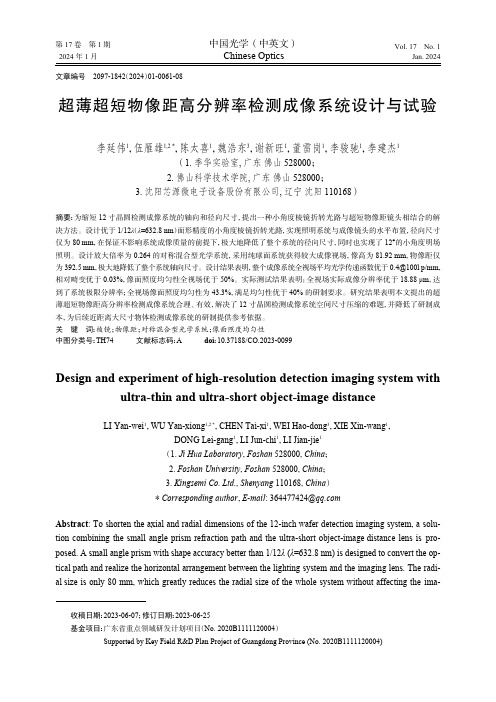
文章编号 2097-1842(2024)01-0061-08超薄超短物像距高分辨率检测成像系统设计与试验李延伟1,伍雁雄1,2 *,陈太喜1,魏浩东3,谢新旺1,董雷岗1,李骏驰1,李建杰1(1. 季华实验室, 广东 佛山 528000;2. 佛山科学技术学院, 广东 佛山 528000;3. 沈阳芯源微电子设备股份有限公司, 辽宁 沈阳 110168)摘要:为缩短12寸晶圆检测成像系统的轴向和径向尺寸,提出一种小角度棱镜折转光路与超短物像距镜头相结合的解决方法。
设计优于1/12λ(λ=632.8 nm )面形精度的小角度棱镜折转光路,实现照明系统与成像镜头的水平布置,径向尺寸仅为80 mm ,在保证不影响系统成像质量的前提下,极大地降低了整个系统的径向尺寸,同时也实现了12°的小角度明场照明。
设计放大倍率为0.264的对称混合型光学系统,采用纯球面系统获得较大成像视场,像高为81.92 mm ,物像距仅为392.5 mm ,极大地降低了整个系统轴向尺寸。
设计结果表明,整个成像系统全视场平均光学传递函数优于0.4@100l p/mm ,相对畸变优于0.03%,像面照度均匀性全视场优于50%。
实际测试结果表明:全视场实际成像分辨率优于18.88 μm ,达到了系统极限分辨率;全视场像面照度均匀性为43.3%,满足均匀性优于40%的研制要求。
研究结果表明本文提出的超薄超短物像距高分辨率检测成像系统合理、有效,解决了12寸晶圆检测成像系统空间尺寸压缩的难题,并降低了研制成本,为后续近距离大尺寸物体检测成像系统的研制提供参考依据。
关 键 词:棱镜;物像距;对称混合型光学系统;像面照度均匀性中图分类号:TH74 文献标志码:A doi :10.37188/CO.2023-0099Design and experiment of high-resolution detection imaging system withultra-thin and ultra-short object-image distanceLI Yan-wei 1,WU Yan-xiong 1,2 *,CHEN Tai-xi 1,WEI Hao-dong 3,XIE Xin-wang 1,DONG Lei-gang 1,LI Jun-chi 1,LI Jian-jie 1(1. Ji Hua Laboratory , Foshan 528000, China ;2. Foshan University , Foshan 528000, China ;3. Kingsemi Co. Ltd., Shenyang 110168, China )* Corresponding author ,E-mail : 364477424@Abstract : To shorten the axial and radial dimensions of the 12-inch wafer detection imaging system, a solu-tion combining the small angle prism refraction path and the ultra-short object-image distance lens is pro-posed. A small angle prism with shape accuracy better than 1/12λ (λ=632.8 nm) is designed to convert the op-tical path and realize the horizontal arrangement between the lighting system and the imaging lens. The radi-al size is only 80 mm, which greatly reduces the radial size of the whole system without affecting the ima-收稿日期:2023-06-07;修订日期:2023-06-25基金项目:广东省重点领域研发计划项目(No. 2020B1111120004)Supported by Key Field R&D Plan Project of Guangdong Province (No. 2020B1111120004)第 17 卷 第 1 期中国光学(中英文)Vol. 17 No. 12024年1月Chinese OpticsJan. 2024ging quality. At the same time, a small angle of 12° bright field lighting is realized. A symmetrical hybrid op-tical system with magnification of 0.264 is designed. A pure spherical system is used to obtain a large ima-ging field of view. The image height is 81.92 mm, and the object-image distance is only 392.5 mm, which greatly reduces the axial size of the whole system. The design results show that the average optical transfer function of the whole imaging system is better than 0.4@100 lp/mm, the relative distortion is better than 0.03%, and the uniformity of the image surface illuminance is better than 50%. The actual test results show that the actual imaging resolution is better than 18.88 μm, which reaches the ultimate resolution of the sys-tem. The uniformity of illumination of image surface is 43.3%, which meets the development requirement of uniformity better than 40%. The research results show that the ultra-thin and ultra-short object-image dis-tance imaging system is reasonable and effective, which solves the problem of space size compression of the 12-inch wafer detection imaging system and reduces the development cost. It provides a reference for the de-velopment of the imaging system for detecting large objects in short distance.Key words: prism;object-image distance;symmetric hybrid optical system;image surface illumination uni-formity1 引 言自动光学检测(AOI)系统[1-6]是半导体检测设备的重要组成部分,可用于实现对涂胶显影后的12寸晶圆表面缺陷的全范围检测(Full Scale Scan)。
丝素蛋白@二氧化钛复合光电忆阻器的构筑和性能研究

丝素蛋白@二氧化钛复合光电忆阻器的构筑和性能研究
赵飞翔;张艺;范苏娜;张耀鹏
【期刊名称】《合成技术及应用》
【年(卷),期】2022(37)4
【摘要】生物光电忆阻器可集成光学感知、非易失存储和突触模拟等功能,被认为是人工视觉系统的重要构建基元之一。
生物材料因具有良好的生物相容性、生物可降解性和可持续性,被广泛用于光学材料中。
本文采用共混的方式制备了丝素蛋白(SF)@二氧化钛(TiO_(2))复合忆阻功能层,以氧化铟锡玻璃(ITO)作为底电极,金属银阵列作为顶电极,构筑了SF基生物光电忆阻器。
研究发现,在SF中掺杂少量的TiO_(2)可显著提升忆阻器的循环稳定性。
同时,得益于SF@TiO_(2)忆阻功能层在300~380 nm之间较强的紫外光吸收,该复合器件在紫外光照射下具有明显的忆阻电流响应,启动电压(V SET)和置位电压(V RESET)显著降低。
这是由于光照作用导致的空穴-电子对分离,提高了薄膜中载流子的传输效率。
通过拟合I-V曲线可知,该复合器件的忆阻机制为Pool-Frenkel发射机制。
【总页数】7页(P32-38)
【作者】赵飞翔;张艺;范苏娜;张耀鹏
【作者单位】东华大学材料科学与工程学院
【正文语种】中文
【中图分类】TQ322.4
【相关文献】
1.仿生超疏水聚丙烯/二氧化钛复合薄膜的构筑及性能研究
2.石墨烯/二氧化钛复合催化剂制备及光电催化性能研究
3.蛋白质基忆阻器研究进展
4.镍-二氧化钛核壳复合微球的制备及其光电性能研究
5.丝素蛋白气凝胶/聚羟基聚氨酯类玻璃高分子复合材料的制备及其性能研究
因版权原因,仅展示原文概要,查看原文内容请购买。
- 1、下载文档前请自行甄别文档内容的完整性,平台不提供额外的编辑、内容补充、找答案等附加服务。
- 2、"仅部分预览"的文档,不可在线预览部分如存在完整性等问题,可反馈申请退款(可完整预览的文档不适用该条件!)。
- 3、如文档侵犯您的权益,请联系客服反馈,我们会尽快为您处理(人工客服工作时间:9:00-18:30)。
a r X i v :c o n d -m a t /0410240v 1 [c o n d -m a t .m t r l -s c i ] 10 O c t 2004Ultrathin epitaxial graphite:2D electron gas properties and a route toward graphene-basednanoelectronics.Claire Berger,∗Zhimin Song,Tianbo Li,Xuebin Li,Asmerom Y .Ogbazghi,Rui Feng,Zhenting Dai,Alexei N.Marchenkov,Edward H.Conrad,Phillip N.First,and Walt A.de HeerSchool of Physics,Georgia Institute of Technology,Atlanta,GA 30332-0430(Dated:October 7,2004)We have produced ultrathin epitaxial graphite films which show remarkable 2D electron gas (2DEG)behavior.The films,composed of typically 3graphene sheets,were grown by thermal decomposition on the (0001)surface of 6H-SiC,and characterized by surface-science techniques.The low-temperature conductance spans a range of localization regimes according to the structural state (square resistance 1.5k Ωto 225k Ωat 4K,with positive magnetoconductance).Low resistance samples show characteristics of weak-localization in two dimensions,from which we estimate elastic and inelastic mean free paths.At low field,the Hall resistance is linear up to 4.5T,which is well-explained by n -type carriers of density 1012cm −2per graphene sheet.The most highly-ordered sample exhibits Shubnikov -de Haas oscillations which correspond to nonlinearities observed in the Hall resistance,indicating a potential new quantum Hall system.We show that the high-mobility films can be patterned via conventional lithographic techniques,and we demonstrate modulation of the film conductance using a top-gate electrode.These key elements suggest electronic device applications based on nano-patterned epitaxial graphene (NPEG),with the potential for large-scale integration.The exceptional electronic transport properties of low-dimensional graphitic structures have been amply demon-strated in carbon nanotubes and nanotube-based transistors.Ballistic transport has been observed up to room temperature [1,2,3],and quantum interference e ffects at cryogenic tem-peratures [4,5,6].Simple nanotube transistors [7,8],and interconnected logic gates [9]have been demonstrated,which rely on the ability to control the nanotube conductance via an electrostatic gate.The basic transport parameters of these de-vices are so compelling that nanotubes are considered to be a candidate material system to eventually supplant silicon in many electronic devices.An under-appreciated fact is that most electronic proper-ties of carbon nanotubes are shared by other low-dimensional graphitic structures.For example,planar nanoscopic graphene ribbons (i.e.ribbons of a single sheet of graphite)have been studied theoretically [10,11],and they exhibit properties that are similar to nanotubes.Graphene ribbons with either metallic or semiconducting electronic structure are possible,depending on the crystallographic direction of the ribbon axis [10].Thus,if suitable methods were developed to support and align graphene sheets,it would be possible to combine the advantages of nanotube-like electronic proper-ties with high-resolution planar lithography to achieve large-scale integration of ballistic devices.An essential di fference between nanotubes and planar graphene ribbons is the pres-ence of dangling bonds at the edges.Normally these would be hydrogen-terminated,with little influence on the valence electronic properties.However,edge atoms could be passi-vated with donor or acceptor molecules,thus tuning the elec-tronic properties without a ffecting the graphitic backbone of the device.This Letter presents recent results [12]that show the two-dimensional nature of electrical transport in ultrathin graphite (multilayered graphene)grown epitaxially on SiC(0001).6H-SiC is a large bandgap (3eV)semiconductor,which providesan insulating substrate at temperatures below 50K for the n -type (nitrogen)doping employed here.We use magnetocon-ductance measurements and the physics of weak-localization to determine transport parameters of the graphite 2D electron gas (2DEG),and we show that the character of the magne-totransport /localization spans a wide range of behaviors,de-pending on the amount of disorder in the film or substrate.Quantum oscillations in the magnetoconductance and in the Hall resistance are found for the most ordered sample.The character of these features suggests that the quantum Hall ef-fect could be observed at lower temperatures,higher fields,or in ultrathin graphite films of only slightly higher mobility.To our knowledge,these are the first transport measurements on oriented and patterned graphite films of only a few monolay-ers thickness (hence “graphene”films),although related trans-port experiments have been done on thicker (65–100graphene layers)free-standing graphite microdisks,which were nano-patterned by focused-ion-beam (FIB)lithography [13].Given the large mean free paths measured in high-quality graphites [14],the unusual electronic dispersion of graphene,and the fact that the carriers lie near an air-exposed surface,this unique 2DEG system holds great scientific potential.Fur-thermore,with su fficiently high-quality material,ballistic and coherent devices analogous to nanotube designs [15]would be possible.This goal requires that the epitaxial graphene can survive the processing necessary for creation of submicron ribbons [10,11],and that the 2DEG can be gated electrostat-ically.Below we also demonstrate these critical elements for the realization of electronic devices based on nano-patterned epitaxial graphene (NPEG).Ultrathin epitaxial graphite films were produced on the Si-terminated (0001)face of single-crystal 6H-SiC by thermal desorption of Si [16,17,18,19].After surface preparation by oxidation [20]or H 2etching [21],samples were heated by electron bombardment in ultrahigh vacuum (UHV;base pres-sure 1×10⁻¹⁰Torr)to ∼1000◦C in order to remove the ox-2FIG.1:(a)-(d)LEED patterns from Graphite/SiC(0001).The sam-ple was heated several times to successively higher temperatures.(a) 1050◦C for10min.Immediately after oxide removal,showing SiC 1×1pattern at177eV.AES C:Si ratio1:2.(b)1100◦C,3min.The√3reconstruction is seen at171eV.AES ratio1:1.9.(c) 1250◦C,20min.109eV pattern showing diffracted beams from the 6√3unit cell.Examples offirst-order SiC and graphite spots are marked.Note the surrounding hexagons of“6×6”spots.AES C:Si ratio2:1(∼1ML graphite).(d)1400◦C,8min.98eV LEED pattern.AES ratio7.5:1(∼2.5ML graphite).(e)STM image of a surface region of the sample described in Fig.1d.Inset:Atomically-resolved region(different sample,similar preparation).(f):dI/dV spectra(log scale)acquired from the regions marked with corre-sponding line types in the image at top.The solid line is an aver-age of396spectra at different positions,the dashed line an average of105.With a few“glitchy”exceptions,individual spectra in each region showed negligible variation from the average dI/dV shown.ide(some samples were oxidized/de-oxidized several times to improve the surface quality).Scanning force microscopy im-ages showed that the best initial surface quality was obtained with H2etching(sample A).After verifying by Auger elec-tron spectroscopy(AES)that the oxide was removed,samples were heated to temperatures ranging from1250◦C to1450◦C for1–20min.Under these conditions,thin graphite layers are formed[16,17,18],with the layer thickness determined pre-dominantly by the temperature.Multilayered-graphenefilm thicknesses were estimated by modeling the ratio of measured intensities in the Si92-eV and C271-eV Auger peaks(3keV incident energy)[22,23,24].Figures1(a)–(d)show low energy electron diffraction pat-terns(LEED)at different stages during the growth of a2.5-monolayer(ML)graphitefilm grown in-situ.Figure1e dis-plays an STM image from the sample obtained after stage(d). The image reveals a distinct6×6corrugation of the over-layer[25]and a raised region along a step on the surface. This modulation has been previously attributed to variations of the interlayer interaction arising from Moirécoincidences between the graphite and SiC lattices within a fundamental 6√3surface unit cell[16,25,26,27].LEED confirms that the graphene sheets register epitaxially with the underly-ing SiC,as shown in Figs.1c and1d.The mean height dif-ference between terraces(0.25nm),indicates that the step in Fig.1e is a bilayer step in the SiC substrate.Terrace sizesSample C:Si Thickness R4K MobilityA103ML 1.5kΩ1100cm2/VsB∞>5 2.2C9322D1033315E93225F7 2.5TABLE I:Sample properties.Ratio of intensities in the C(271eV) and Si(92eV)AES peaks,calculated thickness in graphene mono-layers,square resistance at4K,and mobility(where measured). (corresponding to a single6×6domain)are found by STM to be up to several hundred nanometers in extent.Preliminary high-resolution LEED studies indicate that the graphene lay-ers are strained in-plane by0.3–0.5%,with a mean structural coherence length of greater than20nm.Also shown in Fig.1f are derivative tunneling spectra (dI/dV vs.V)acquired within the respective boxed regions of the image.The dI/dV spectrum obtained from the lower terrace(solid line)is consistent with that of a zero-gap semi-conductor,as found typically for bulk graphite.On the upper terrace,the6×6domain images somewhat differently,and the dI/dV spectrum(dashed line)displays a region of con-stant,finite conductance around the Fermi energy(zero bias). Spectral shapes are very uniform within each6×6domain. The dI/dV curves show that the electronic properties of the film are not entirely homogeneous.This may relate to dif-fering lateral registry(i.e.not orientational)of the graphite on the SiC substrate,or electron confinement within6×6 domains.dI/dV spectra acquired over the buckled region at the step edge are nearly identical to those found on the upper terrace,suggesting that the graphite layer remains continuous over the step.DC and low-frequency AC conductance measurements were made for temperatures T=0.3–50]K,and for mag-neticfields H from0–8T on graphitefilms with thicknesses of typically3graphene sheets(see Table I).For Hall-effect measurements,samples were defined using standard optical lithography(photoresist coating,plasma etching,photoresist removal via solvents).Four contacts were painted with sil-ver paste directly on the surface or on evaporated Pd-Au pads on mm-size samples.For samples B,C and E,the voltage probe distance d V is2mm.For the Hall bar samples A and D d V=600and300µm respectively(see photo inset,Fig.2a). Reported values below are the square conductance G.The2D nature of electrical transport in thefilm is vividly demonstrated in Fig.2a by the large anisotropy in the mag-netoconductance[MC=G(H)]:For H perpendicular to the graphene plane the differential magnetoconductance(dMC= dG/dH)is large and positive(3.0µS/T at4K),whereas there is essentially no response when H lies in the plane(in-plane MC was measured with H transverse to the current direction). This anisotropy is found in all of our samples,and indicates3Temperature (K)Conductance(µS)(b)FIG.2:(a)Magnetoconductance G(H)for samples E,C and A inperpendicularfield for temperatures as indicated.Also shown forsamples E and C,the in-plane magnetoconductance at5K.Note thestrong anisotropy between the perpendicular and in-planefield con-figuration.In sample C,the conductance goes through a maximumat about the same value offield and conductance for all T.In sampleA Shubnikov-de Haas oscillations develop at high magneticfield.Center-panel inset:G(H)−G(H=0)for sample B.Solid curvearefits to the weak localization theory with no spin-orbit,yieldingelastic scattering lengthℓe≈15nm and inelastic scattering lengthℓi(4K)≈100nm.Lower-panel inset:Hall resistance R xy=V xy/iand magnetoresistance R xx as a function of magneticfield at4K forsample A.Below4.5T,R xy is remarkably linear,indicative of n-typecarriers.At high magneticfield,the oscillations coincide with theoscillations in the magnetoresistance.(b)Square conductance as afunction of temperature for samples of various conductance(sam-ples A,B,C,D and E from top to bottom).Note that the conduc-tance scale is×4for samples D and E,compared to the scale forsample A-C.Samples A,B and C show a ln T form in this decade oftemperature,characteristic of2D weak localization.that the motion of charge carriers is confined to the grapheneplanes.The observed positive dMC is in contrast to bulkgraphite[28],which shows negative dMC for well-orderedsingle-crystals,and also a large anisotropy.However,car-bon foils fabricated from exfoliated graphite[29]and partiallygraphitic carbons[30]have positive MCs initially,which be-come negative at largefields.This behavior is a consequenceof disorder-induced localization in the sample.Figure2a shows systematic changes in the perpendicu-lar MC for samples of successively larger zero-field conduc-tance(i.e.decreasing disorder).For sample C the initial4K slope is larger,at30µS/T,and the MC attains an ap-proximately temperature-independent maximum of185µS atH≈3.5T.Sample A shows even more structure.Followinga large initial dMC(500µS/T at4K),the MC maximizes near1.5T,then decreases,followed by a series of(Shubnikov-deHaas)oscillations.A temperature-independent“fixed point”at G=680µS and H=7.4T is also observed.As a function of temperature,the conductance increasesproportional to ln T at low T,as shown in Fig.2b for samplesA–C.This is quite characteristic of a2D electron gas in theweak localization regime[31,32].The least conductive sam-ples(D and E;G<e2/h=38.8µS)deviate slightly from theln T dependence,which is indicative of a transition to stronglocalization[see for instance Ref.33].In a2D system,carriers will localize at low temperature dueto constructive quantum interference of time-reversed pathsfor carriers scattered elastically from static disorder[31].Theinterference is reduced(conductance increased)by breakingtime-reversal symmetry through the application of a magneticfield,or by increasing temperature.These coherent effects aremanifest when the elastic mean free pathℓe is smaller than theinelastic mean free pathℓi(T).For k Fℓe≫1(k F is the Fermiwave vector),the system is in the weak localization regime.Strong localization occurs for smaller k Fℓe[33,34].Shown in the center-panel inset of Fig.2a is the perpendic-ular MC of sample B forfive different temperatures(circles),andfits to the data according to2D weak-localization theory(lines)[32].The entire family of MC curves isfit by a singletemperature-dependent parameter,ℓi(T).Note that for trans-port in two dimensions,the mean free paths are obtained fromthe modeling without knowledge of either the Fermi velocityor the carrier effective mass.For sample B,wefindℓe=15nmandℓi=100nm at T=4K.Weak localization effects are ob-served over a much smaller range of magneticfield for sampleA,but a similar estimate givesℓe=20–30nm,and a muchlarger inelastic mean free pathℓi(4K)∼300nm.From thecarrier density n=1012cm−2per graphene sheet(see below),wefind for sample A k Fℓe∼5,in agreement with the weaklocalization regime.In two cases we have observed a reversal of the dMC.Atthe maximum MC for sample C(Fig.2a),the conductance pergraphene sheet(Table I)is1.5e2/h,parable to the con-ductance quantum.This behavior,and the large change in MCof this sample(550%)are reminiscent of disordered2DEGs,which have been explained in terms of a transition from anAnderson insulator to a quantum Hall liquid[35].The secondcase is that of sample A,which underwent an improved sub-strate preparation.For this sample,we also observe an initialmaximum in the MC,but at much lowerfield(1.5T).Appar-ently weak-localization dominates the MC behavior of sampleA in the low-field region,but the longer scattering paths aredephased by a smaller magneticfield.The subsequent appear-ance of Shubnikov-de Haas oscillations indicates quantizationof the electron energy spectrum,and wave function coherenceon a scale comparable to the cyclotron radius(∼30nm at5T),which is consistent with the elastic scattering lengthsestimated above.The significance of the quasi-temperature-independentfixed point at680µS and afield of7.4T is notyet fully understood.Note that1/H at the crossing point is4 equal to the mobility obtained from Hall measurements(seebelow).This correspondence would be an expected conse-quence of electron-electron interactions under weak localiza-tion[33,36],but the observed quantum oscillations show thatat highfields the system is beyond this regime.The Hall resistance R xy was measured for samples D andA in the Hall bar configuration(photo inset,Fig.2a)at abias current of100nA.For sample D at4K,R xy versus His linear from0to8T,with the slope corresponding to a den-sity n=1013cm−2n-type charge carriers,and a mobility of 15cm2/Vs.The Hall voltage is also linear up to4.5T in sam-ple A,from which we determine n=3.6×1012cm−2(n-type), and an enhanced mobility of1100cm2/Vs.The observation of a linear Hall effect is particularly remarkable,since single-crystal graphite samples display a substantial quadratic com-ponent at smallfields[29,37,38,39],due to three sub-bands (one electron,two hole).Apparently,our samples cannot be thus described.The carrier densities found here are compa-rable to those of other2DEG systems,although the density per graphene sheet(∼1012cm−2)is higher than that found in high-quality graphites[28,38,39].It remains to be deter-mined what effect substrate doping has on the carrier density and mobility in the graphitefilm.For the case of sample A,a carrier density can be obtained from the period(in1/H)of the Shubnikov-de Haas oscilla-tions.Assuming a circular2D Fermi surface,we estimate n=1012cm−2(k F=2.5×106cm−1).The carrier den-sity determined by the Hall effect is very nearly a factor3 larger,which is the number of graphene layers measured via AES.Clearly,the simplest explanation would be that each graphene sheet supports a2D electron gas which remains con-fined within the sheet.This would be consistent with the large anisotropy in conductivity for bulk graphite[28].The tem-perature dependences of samples A–C also support this inter-pretation:dG/d(ln T)falls between2.5e2/πh and3.5e2/πh, about a factor3larger than the predicted weak-localization contribution to the conductance,3.5(e2/πh)ln T[32]. Above4.5T in sample A,we observe nonlinearities in R xy vs.H,as shown in Fig.2a(lower-panel inset)for T=4K. These coincide with the Shubnikov-de Haas oscillations in the magnetoconductance,showing that they have the same origin: Either broadened quantum Hall plateaus,or bulk magneto-quantum oscillations in a metallic system.If the Hall con-ductance at the location of the local maximum(≈5.5T)is normalized with respect to the number of sheets,one obtains a conductance≈4e2/h which suggests a quantum Hall ef-fect(see also predictions in Ref.40).Experiments at lower temperatures and higherfields will be necessary to verify this conjecture.At0.3K,we also observe a pronounced zero-bias anomaly in the highly resistive sample D.The conductance is found to increase by about a factor10as the bias voltage is increased from0to25mV[41].For weak electron-electron interactions it can be understood in terms of enhanced scattering of carri-ers near the Fermi energy:the wavelengths of these carriers are commensurate with the Friedel oscillations surroundingGate Voltage (V)Conductance(µS)FIG.3:Conductance as a function of gate voltage for sample F at 4K.Inset,sketch of the sample showing the contacts and top-gate geometry(S,D,G=source,drain,gate).The top-gate is only par-tially effective due to the open geometry.Nevertheless,a2%change in conductance is observed.impurities,thus they scatter strongly.The coherence is lost at higher bias(higher kinetic energies).Zero-bias anomalies have also been observed in carbon nanotubes[42,43,44].It should be noted that the samples are remarkably stable over time.For instance,measurements in Figs.2a and2b were made4months earlier than those in the lower-panel in-set of Fig.2a,with no particular storage precautions.The features observed are essentially the same,except for a slight decrease in conductance and carrier density.The results pre-sented above for sample A also show that the multi-sheet epi-taxial graphenefilm survives conventional lithographic pro-cessing extraordinarily well.Finally,as a preliminary demonstration of the device po-tential of this new2DEG system,a large-area gated graphite-channelfield-effect transistor(FET)structure was assembled.A schematic of the“device”is shown in Fig.3,as well as the measured source-drain resistance as a function of gate volt-age.The top-gate structure consisted of a conductive coat-ing on a100-nm-thick insulating aluminum oxide layer.The gate covered only a portion of the graphitefilm between the source and drain electrodes,leaving large ungated leakage paths(see inset,Fig.3).Consequently,the resistance mod-ulation is rather small(2%),but these results show clearly that multi-sheet epitaxial graphenefilms can be gated,in dis-tinct contrast to thicker samples[45].Thus we anticipate that FET-type devices will be possible,particularly when the chan-nel electronic structure is controlled by patterning the graphite into a narrow strip[10,13,46].The experimental results presented here demonstrate the rich scientific promise of ultrathin epitaxial graphite (“graphene”)films.Several points should be appreciated: First,the production method allows graphiticfilms to be grown epitaxially,as evidenced by LEED and STM measure-ments.From Auger spectroscopy we further conclude that the layers involve only a few graphene sheets.Remarkably, thefilms are electrically continuous over several mm.Magne-toconductance measurements clearly reveal2D electron gas properties,including large anisotropy,high mobility,and2D localization,in samples patterned by conventional lithogra-5phy.Quantum oscillations observed in both the magneto-conductance and the Hall resistance indicate a potential new quantum Hall system.Finally,control of the2D electron gas carrier density via electrostatic gating was also demonstrated. Considered with prior research in graphitic systems,these results provide ample evidence that the graphite/SiC system could provide a platform for a new breed of seamlessly-integrated ballistic-carrier devices based on nano-patterned epitaxial graphene.Such an architecture could have many advantages for nanoelectronics,including potentially coher-ent devices,energy efficiency,and facile integration with molecular devices.This work was funded by Intel Research and by the De-partment of Energy(DE-FG02-02ER45956).Support from Georgia Tech,CNRS-France,and the NSF(ECS-0404084), is also gratefully acknowledged.We thank Drs.Thierry Klein,Jacques Marcus and Frédéric Gay,CNRS-LEPES, Grenoble-France,for their generosity in allowing us to use their cryostats,and Dr.P.G.Neudeck,NASA Glenn Research Center,for supplying the sample used in Fig.1.We are espe-cially grateful to Dr.Thierry Grenet for providing invaluable assistance in obtaining the data in Fig.3.∗Permanent address:CNRS-LEPES,BP166,38042Grenoble Cedex,France.[1]S.Frank,P.Poncharal,Z.Wang,and W.D.Heer,Science280,1744(1998).[2]P.Poncharal et al.,Journal of Physical Chemistry B106,12104(2002).[3]W.Liang et al.,Nature411,665(2001).[4]S.Tans et al.,Nature386,474(1997).[5]A.Bachtold et al.,Nature397,673(1999).[6]C.Schönenberger et al.,Applied Physics A(Materials ScienceProcessing)A69,283(1999).[7]S.Tans,R.Verschueren,and C.Dekker,Nature393,49(1998).[8]R.Martel et al.,Applied Physics Letters73,2447(1998).[9]A.Bachtold,P.Hadley,T.Nakanishi,and C.Dekker,Science294,1317(2001).[10]K.Wakabayashi,Phys.Rev.B64,125428(2001).[11]K.Nakada,M.Fujita,G.Dresselhaus,and M.Dresselhaus,Phys.Rev.B54,17954(1996).[12]C.Berger et al.,Bull.Am.Phys.Soc.49,A17.8(2004).[13]E.Dujardin,T.Thio,H.Lezec,and T.Ebbesen,Appl.Phys.Lett.79,2474(2001).[14]Y.Kaburagi,A.Yoshida,and Y.Hishiyama,J.Mat.Res.11,769(1996).[15]A.Javey et al.,Nature424,654(2003).[16]A.V.Bommel,J.Crombeen,and A.V.Tooren,Surf.Sci.48,463(1975).[17]A.Charrier et al.,J.Appl.Phys.92,2479(2002).[18]I.Forbeaux,J.-M.Themlin,and J.-M.Debever,Phys.Rev.B58,16396(1998).[19]Samples for transport measurements were obtained from Cree,Inc.,Durham,NC(research grade,n-doped,0.05Ω-cm).Fig-ures1and2show LEED and STM data from a sample with a1-µm CVD layer grown at the NASA Glenn Research Cen-ter.The CVD sample was initially much smoother than the as-received Cree sample.However,after oxidation/graphitization cycles samples were found via LEED and STM to be similar, although the CVD sample was still of higher overall surface quality.[20]M.-H.Cho et al.,J.Vac.Sci.Technol.A21,1004(2003).[21]V.Ramachandran et al.,J.Elec.Mater.27,308(1998).[22]T.Li,A.Y.Ogbazghi,and P.N.First,to be published(unpub-lished).[23]S.Tanuma,C.J.Powell,and D.R.Penn,Surface and InterfaceAnalysis17,911(1991).[24]S.Tanuma,C.J.Powell,and D.R.Penn,Surface and InterfaceAnalysis17,927(1991).[25]M.-H.Tsai,C.Chang,J.Dow,and I.Tsong,Phys.Rev.B45,1327(1992).[26]U.Starke et al.,Materials Science Forum264-268,321(1998).[27]F.Owman and P.Martensson,Surf.Sci.369,126(1996).[28]D.E.Soule,J.W.McClure,and L.B.Smith,Phys.Rev.134,A453(1964).[29]R.V.Schaijk et al.,Phys.Rev.B57,8900(1998).[30]V.Bayot et al.,Phys.Rev.B41,11770(1990).[31]E.Abrahams,P.Anderson,D.Licciardello,and T.Ramakrish-nan,Phys.Rev.Lett.42,673(1979).[32]G.Bergmann,Phys.Rep.107,1(1984).[33]G.Minkov et al.,Phys.Rev.B65,235322(2002).[34]The strong localization regime is not discussed in detail here,but we note that for samples D and E,measurements in the range0.3–2K show ln(G)∼T−1/3,a form that is consistent with theories of strong localization in2D[47].[35]H.Jiang,C.Johnson,K.Wang,and S.Hannahs,Phys.Rev.Lett.71,1439(1993).[36]B.Altshuler and A.Aronov,in Electron-electron interactions indisordered systems,edited by A.L.Efros and M.Pollak(North-Holland,Leningrad Nucl.Phys.Inst.,USSR,1985),pp.1–153.[37]T.G.Berlincourt and M.C.Steele,Phys.Rev.98,956(1955).[38]X.Du,S.-W.Tsai,D.L.Maslov,and A.F.Hebard,arXiv:cond-mat/0404725v191(2004).[39]T.Tokumoto et al.,m.129,599(2004).[40]Y.Zheng and T.Ando,Phys.Rev.B65,245420(2002).[41]Samples were carefully mounted with the connecting wiresthermally connected by stycast epoxy to the cooled copper plate.This mounting provided more than sufficient thermal cou-pling to assure that the maximum power into the sample(10 nW)did not cause significant heating.[42]M.Bockrath et al.,Nature397,598(1999).[43]R.Tarkiainen et al.,Phys.Rev.B64,195412(2001).[44]W.Yi et al.,Phys.Rev.Lett.91,076801(2003).[45]H.Kempa and E.Esquinazi,arXiv:cond-mat/03041051(2003).[46]L.Can˛cado et al.,Phys.Rev.Lett.93,047403(2004).[47]N.F.Mott,Conduction in Non-Crystalline Materials(OxfordUniversity Press,New York,1987).。