TXB0108ZXYR中文资料
产品介绍zxcvbn

18
针、纺织类 孚日清影双条毛巾礼盒
序号:19 中心总序号:193 产品编号:1500068 采购方式:原有保留定向 市场参考价:72.00元 淘宝参考价:25.92元 义乌交货价(含税): 23.20元 物流费率:1.8% 员工采购总价(含物流费):23.62 元 价格有效期:2012年7月31日 品牌:孚日 型号:FRTG-1013F 规格:34*75cm*2 产品说明: 1.透气性高:100%优质纯棉面料,良好的吸湿透 气性,轻便不黏身。2.亲肤性优:手感柔软,毛圈蓬 松,让肌肤时刻享受纯棉的柔软和舒适。3.色牢度好: 染色全部使用进口活性染料,耐洗涤。
7
日用品类 天堂高密聚酯银胶三折铅笔伞
序号:8 中心总序号:64 产品编号:2100047 采购方式:原有保留定向 市场参考价:65.00元 淘宝参考价:43.00元 义乌交货价(含税):20.80元 物流费率:1.8% 员工采购总价(含物流费):21.17 元 价格有效期:2012年7月31日 品牌:天堂 型号:3336E 规格:52cm/6k 产品说明: 三折铅笔伞,超细小,银胶面料遮阳效果极佳,伞面 图案时尚浪漫。
14
五金及电料类 维氏军刀套装
序号:15 中心总序号:159 产品编号:1600036 采购方式:原有保留定向 市场参考价:328.00元 淘宝参考价:199.00元 义乌交货价(含税): 169.00元 物流费率:1.8% 员工采购总价(含物流费):172.04 元 价格有效期:2012年7月31日 品牌:VICTORINOX 型号:VI-05GB03 规格:维氏1.3703瑞士军刀+皮套;包装尺寸 20.6*15.6*5.4cm 产品说明: 产品包括:大刀、小刀、拔木塞钻、开罐头器 (兼附)、开瓶器(兼附)、钻孔锥、钥匙圈、镊子、 牙签、剪刀、多用途勾、改锥(3毫米)、改锥(5毫米)、 电线剥皮槽。
txb0108pwr的用法
txb0108pwr的用法
"txb0108pwr"通常指的是一种集成电路芯片,用于逻辑电平转换。
这种芯片通常被用于将不同电平的信号进行转换,例如3.3V和5V之间的转换。
它可以用于连接不同电平的设备,如微控制器、传感器、存储器等,以确保它们能够正确地进行通信和交互。
在实际应用中,"txb0108pwr"通常具有以下用法:
1. 电平转换,将高电平转换为低电平或者将低电平转换为高电平,以适配不同设备之间的电平标准。
2. 信号隔离,在一些场合下,需要隔离不同电路之间的信号,以避免电气干扰或者保护电路。
3. 电压匹配,将不同电压的信号匹配到相应的电路中,以确保电路的正常工作。
"txb0108pwr"通常具有多个引脚,包括输入引脚、输出引脚、电源引脚等。
在使用时,需要根据具体的电路设计和要求正确连接这些引脚,以确保芯片能够正常工作。
总的来说,"txb0108pwr"是一种常用的逻辑电平转换芯片,用于解决不同电平设备之间的兼容性问题,具有广泛的应用场景。
RDS82580XXOO中文资料

FEATURES:Low On-State VoltageHermetic Ceramic Package Excellent Surge and I 2t RatingsAPPLICATIONS:DC Power Supplies ORDERING INFORMATIONInput Rectifiers Plating SuppliesSelect the complete 12 digit Part Number using the table below.EXAMPLE: RDS82280XXOO is a 2200V-8000A General Purpose DiodeRevised:916/2002Powerex General Purpose Rectifier Diodes are designed with high locking voltage capability and low forward voltage drop to minimize conduction losses. These are packaged in hermetic, ceramic Pow-R-Disc packages which can be mounted using commercially available clamps and heatsinks or fully assembled to a variety of air or water cooled heat exchangers.Absolute Maximum RatingsCharacteristic Symbol Rating UnitsRepetitive Peak Reverse Voltage V RRM2500VoltsNon-repetitive Transient Peak Reverse Voltage V RSM V RRM + 100VoltsAverage On-State Current, T C=90°C I F(Avg.)8000ARMS On-State Current, T C=90°C I F(RMS)12566APeak One Cycle Surge Current, 60Hz, V R=V RRM I FSM100,000AFuse Coordination I2t, 60Hz I2t 4.17E+07A2s Peak One Cycle Surge Current, 50Hz, V R=0V I FSM92,500AFuse Coordination I2t, 50Hz I2t 3.57E+07A2s Operating Temperature Tj-40 to+175°CStorage Temperature T Stg.-50 to+200°CApproximate Weight 6.5lb2.95KgMounting Force16,000 - 20,000lbs71.2 - 89.0KnewtonsElectrical Characteristics, Tj=25°C unless otherwise specifiedRatingCharacteristic Symbol Test Conditions min typ max Units Repetitive Peak ReverseLeakage Current ITj=175°C, V RRM=Rated150300maRRMPeak On-State Voltage V FM Tj=175°C, I FM=4000A0.82VV FM Model, Low Level V0Tj=175°C0.654V VFM = V O +r•I FM r15% I FM- π•I FM 3.82E-05ΩV FM Model, High Level V0Tj=175°C0.786V VFM = V O +r•I FM rπ•I FM - I FSM 3.27E-05ΩV FM Model, 4-Term A Tj=175°C0.218 V FM=A + B•Ln(I FM) +B15%I FM - I FSM 5.70E-02 C•(I FM) + D•(I FM)½C 3.14E-05D8.51E-05Reverse Recovery Time t RR Tj=25°C, I FM=400A25µsdi R/dt = 25 A/µsThermal CharacteristicsRatingCharacteristic Symbol Test Conditions min typ max Units Thermal ResistanceJunction to Case RΘjc Double side cooled0.0070.0075°C/WattCase to Sink RΘcs Double side cooled0.0010.0015°C/Watt Thermal Impedance Model ZΘjc Double side cooledZΘjc(t) =Σ(A(N)•(1-exp(-t/Tau(N))))where:N =1234A(N) = 1.426E-049.077E-04 2.373E-03 4.080E-03T au(N) = 2.622E-03 2.313E-02 3.049E-01 3.600E+00。
txb0108 8位双向电压电平转换器
A inputs B inputs
Input clamp current Output clamp current Continuous output current
VI < 0 VO < 0
Continuous current through VCCA, VCCB, or GND
Copyright © 2006–2007, Texas Instruments Incorporated
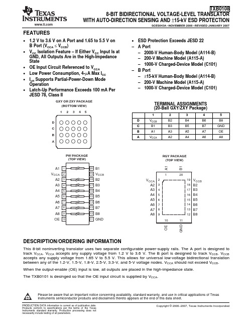
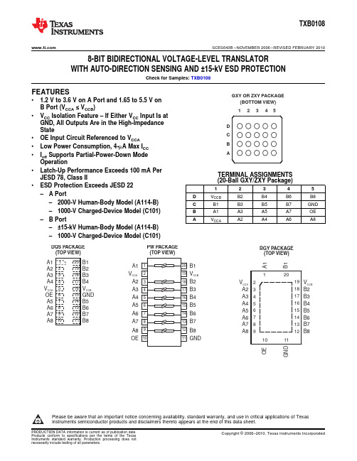
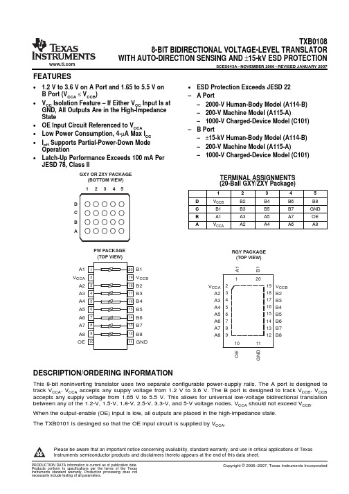
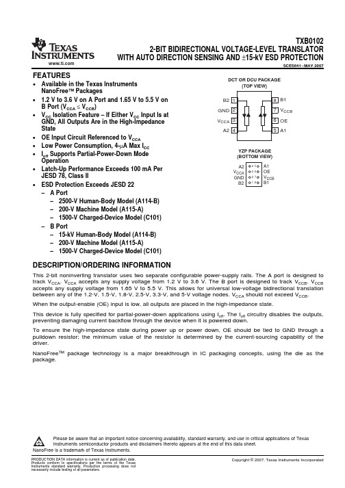
TXB0108 8-BIT BIDIRECTIONAL VOLTAGE-LEVEL TRANSLATOR WITH AUTO-DIRECTION SENSING AND ±15-kV ESD PROTECTION
• OE Input Circuit Referenced to VCCA • Low Power Consumption, 4-µA Max ICC • Ioff Supports Partial-Power-Down Mode
Operation
• Latch-Up Performance Exceeds 100 mA Per JESD 78, Class II
20
B1
Input/output 1. Referenced to VCCB.
2
Submit Documentation Feedback
TXB0108 8-BIT BIDIRECTIONAL VOLTAGE-LEVEL TRANSLATOR WITH AUTO-DIRECTION SENSING AND ±15-kV ESD PROTECTION
PIN DESCRIPTION
NO.
NAME
FUNCTION
1
A1
BTB08中文资料
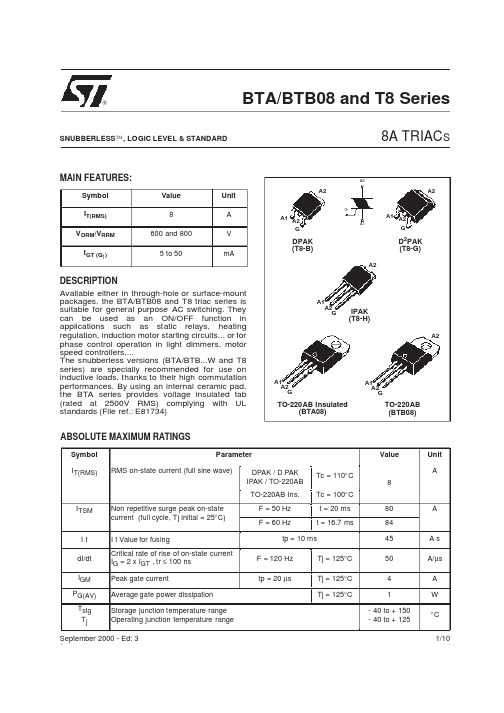
VD = VDRM RL = 3.3 kΩ Tj = 125°C IT = 100 mA IG = 1.2 IGT
■
STANDARD (4 Quadrants)
Symbol Test Conditions Quadrant BTA/BTB08 C IGT (1) V D = 12 V VGT VGD IH (2) IL dV/dt (2) V D = VDRM RL = 3.3 kΩ Tj = 125°C IT = 500 mA IG = 1.2 IGT V D = 67 %VDRM gate open Tj = 125°C Tj = 125°C I - III - IV II MIN. MIN. RL = 30 Ω I - II - III IV ALL ALL MAX. MAX. MIN. MAX. MAX. 25 40 80 200 5 25 50 1.3 0.2 50 50 100 400 10 V/µs V/µs B 50 100 mA V V mA mA Unit
(dV/dt)c (2) (dI/dt)c = 3.5 A/ms
STATIC CHARACTERISTICS
Symbol VTM (2) Vto (2) Rd (2) I DRM I RRM
Note 1: minimum IGT is guaranted at 5% of IGT max. Note 2: for both polarities of A2 referenced to A1
Type Standard Snubberless Standard Snubberless Logic level Logic level Logic level Logic level Snubberless Snubberless Snubberless
sjzl20081074-ZXSDR B8200 C100 技术手册

法律声明
本资料著作权属中兴通讯股份有限公司所有。未经著作权人书面许可,任何单位或个人不得以任何方 式摘录、复制或翻译。
侵权必究。
“ZTE”和“ZTE中兴”是中兴通讯股份有限公司的注册商标。中兴通讯产品的名称和标志是中兴通 讯的专有标志或注册商标。在本手册中提及的其他产品或公司的名称可能是其各自所有者的商标或商 名。在未经中兴通讯或第三方商标或商名所有者事先书面同意的情况下,本手册不以任何方式授予阅 读者任何使用本手册上出现的任何标记的许可或权利。
2.2.4 信道处理模块(CH) ...............................................................................2-7 2.2.5 网络交换模块(FS) ............................................................................... 2-11 2.2.6 环境告警模块(SA) .............................................................................. 2-14 2.2.7 风扇阵列模块(FA) .............................................................................. 2-17 2.2.8 电源模块(PM) .................................................................................... 2-18 2.3 外部线缆及部件................................................................................................ 2-20 2.3.1 GPS天馈系统电缆及部件 ......................................................................... 2-20 2.3.2 以太网线 ................................................................................................ 2-28 2.3.3 光纤 ....................................................................................................... 2-28 2.3.4 数据电缆 ................................................................................................ 2-29 2.3.5 电源系统电缆 ......................................................................................... 2-30 2.3.6 接地系统电缆 .........................................................................................................................................................................2-1
电平转换芯片
Reel of 2000
TXB0108PWR
VFBGA – GXY
Reel of 2500
TXB0108GXYR
VFBGA – ZXY (Pb-free) Reel of 2500
TXB0108ZXYR
TOP-SIDE MARKING YE08 5MR YE08 YE08 YE08
(1) For the most current package and ordering information, see the Package Option Addendum at the end of this document, or see the TI web site at .
To ensure the high-impedance state during power up or power down, OE should be tied to GND through a pulldown resistor; the minimum value of the resistor is determined by the current-sourcing capability of the driver.
TXB0108RGYR中文资料
GXY OR ZXY PACKAGE (BOTTOM VIEW) 1 2 3 45
D C B A
TERMINAL ASSIGNMENTS (20-Ball GXY/ZXY Package)
1
2
3
4
5
D
VCCB
B2
B4
B6
B8
C
B1
B3
B5
B7
GND
B
A1
A3
A5
A7
OE
A
VCCA
A2
A4
A6
A8
PW PACKAGE (TOP VIEW)
PIN DESCRIPTION
NO.
NAME
FUNCTION
1
A1
Input/output 1. Referenced to VCCA.
2
VCCA
A-port supply voltage. 1.1 V ≤ VCCA ≤ 3.6 V, VCCA ≤ VCCB.
3
A2
Input/output 2. Referenced to VCCA.
SCES643A – NOVEMBER 2006 – REVISED JANUARY 2007
TYPICAL OPERATING CIRCUIT
1.8 V
3.3 V
1.8 -V System Controller
Data
VCCA OE
VCCB
TXB0108
A1
B1
பைடு நூலகம்
A2
B2
A3
B3
A4
B4
A5
B5
A6
FEATURES
• 1.2 V to 3.6 V on A Port and 1.65 to 5.5 V on B Port (VCCA ≤ VCCB)
北京煜帮终端维护手册

文档编号:版本号:2010-8-4北京煜帮终端维护手册编制________李庆鑫________审核______________________批准______________________北京煜邦电力技术有限公司2010年08月4日第一部分EDAD2001系列采集器 (4)一、EDAD2001系列采集器介绍 (4)1、基本说明 (4)1.1 ARM版采集器和老版采集器端口的区别 (4)1.2 ARM版采集器单口多规约的设置 (4)2、采集器常用的操作说明 (5)2.1 Linux版采集器操作说明 (5)2.2 DOS版操作说明 (13)2.3 脱硫采集器操作说明........................................ 错误!未定义书签。
3、采集器(DOS版本)文件组成及作用 (15)3.1 可执行程序(C:\EDAD、D:\EDAD) (15)3.2 批处理程序(C:\EDAD、D:\EDAD) (16)3.3 资源文件(C:\EDAD、D:\EDAD) (16)3.4 配置文件(C:\EDAD、D:\EDAD) (16)3.5 数据文件(C:DATA、D:\DATA) (18)4、采集器(Linux版本)文件组成及作用 (18)4.1 /edad目录结构 (19)4.2 /data0及/data1目录结构 (22)5.A采集器的文件组成及作用 (22)二、采集器调试常见问题 (24)1现场调试工作流程 (25)2调试常见问题 (25)2.1 网络通信的调试 (25)2.2 拨号调试注意事项 (27)2.3 召测量的配置方法 (29)2.4 GB645规约电能表的调试 (32)2.5 GPRS通信的调试(来自硬件部提供文档) (34)2.6 采集器网口不够时如何扩充网络功能 (38)2.7 程序升级注意事项 (40)2.8 取得采集器界面密码的方法 (41)2.9 配置文件RATE.INI (41)2.10 关于102规约的调试事项 (42)2.11 关于对时功能的说明 (44)2.12 四象限无功的采集以及负荷曲线的读取 (45)2.13 日冻结与月冻结 (45)2.14 采集器双备份 (46)3、现场调试FAQ(专用) (48)3.1 青海项目调试注意事项 (48)3.2 河北变电站项目调试事项 (50)3.3 河北地电项目的标准配置 (51)3.4 各地不同的特色,比如规约 (52)附件1调制解调器的指示灯及常用指令简介 (52)1.1 MODEM工作状态查看方法: (52)1.2MODEM常用指令 (52)附件2 各地项目文件模板 (54)2.1 河北地电项目CALLBUF.INI文件模板 (54)附件3 FTPHOST远程维护软件使用说明 (65)一、简介 (65)二、准备工作 (65)三、进行远程维护操作 (68)附件4 RemoteConfig3维护软件使用说明 (74)附件 5 采集器资源配置表........................................................ 错误!未定义书签。
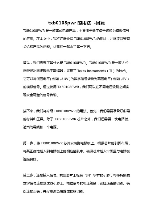
txb0108pwr的用法 -回复
txb0108pwr的用法-回复Txb0108pwr是一种电源控制器芯片,常用于电源系统的设计和控制。
它具有多种功能和特性,使其成为电源管理和优化的重要组成部分。
在本文中,我们将一步一步地回答有关txb0108pwr的用法的问题,并详细介绍它的功能和应用。
第一步:了解txb0108pwr的基本概念和功能作为电源控制器芯片,txb0108pwr具有多种功能和特性,用于管理和优化电源系统。
它主要用于电源开关、调节、保护和监控的各个方面。
以下是它的一些基本功能:1. 电源开关:txb0108pwr可以实现电源的开关控制,通过外部输入信号来实现电源的打开和关闭。
这对于系统的能耗控制和电源的管理至关重要。
2. 电源调节:txb0108pwr可以提供电源稳定和调节功能,可以通过外部反馈信号来监控电源输出,并根据需要进行调整,以保持稳定的电压和电流输出。
3. 电源保护:txb0108pwr具有过流保护、过压保护和过温保护等多种保护功能。
当电源输出过流或压力过高时,它会自动断开电源,以保护电源系统和连接的设备。
4. 电源监控:txb0108pwr可以监控电源的状态和性能,包括输入和输出电压、输出电流等,并提供反馈信号供系统控制和管理。
需要注意的是,txb0108pwr是一种集成电路芯片,需要与其他电路和组件配合使用,才能发挥其功能和效用。
第二步:txb0108pwr的应用领域和场景txb0108pwr广泛应用于各种电源系统中,以满足不同应用的需求。
以下是一些常见的应用领域和场景:1. 电子设备和消费类产品:txb0108pwr可用于智能手机、平板电脑、笔记本电脑等各种电子设备的电源管理和控制,确保其稳定供电和良好性能。
2. 工业自动化和控制系统:在工厂和生产线的控制系统中,txb0108pwr 可以用于电源管理和保护,确保设备的正常运行和稳定工作。
3. 通信和网络设备:txb0108pwr可用于路由器、交换机、服务器等通信和网络设备的电源管理和优化,以提供可靠的供电和稳定的通信性能。
恒通USB增强型防死机智能卡产品使用手册
恒通USB增强型防死机智能卡产品(HT-018)使用手册南京恒超科技有限公司适用设备:基于Windows系统的工控机、监控主机、DVR、触摸屏主机、广告发布机、排号机、电子警察主控机、服务器、PC机等需要长时间稳定运行的设备。
嵌入式系统、linux系统暂不支持。
主要功能:当Windows或监视的应用程序、服务无响应后自动恢复,恢复不成功则自动重启机器。
独有特点:软件采用多任务技术,可同时连续监测128个应用程序或Windows服务。
USB接口芯片采用英国FT公司的工业级产品以确保防死机智能卡硬件的稳定可靠。
独有的计划任务功能设置功能可以定期重新启动电脑以保障系统的稳定。
使用价值:智能监测,灵敏度高;无需人工到达现场手动重启,响应速度快,实现真正的24小时无人值守。
专业设计: 软硬件部分均由专业公司进行的可靠性,稳定性及安全性设计,给客户带来省心放心的防死机效果。
一、系统组成本系统由监测软件(守护精灵V2.0)、硬件板卡及若干连接线组成。
图1 软件界面图2 硬件狗卡板1、USB口2、两个RESET口;3、电源指示灯(D1);4、工作指示灯(D2) 注意:红色电源指示灯(3)亮表示工作正常。
绿色工作指示灯(4)亮表示工作正常;绿灯灭表示当前正在系统设置或系统正在重启或系统没有正常工作。
5、PC-USB端口连接线(红色端接VCC,白色端接GND)6、reset线图3 连接线二、硬件安装(★★★ 安装前请先关闭主机电源 ★★★)第一步:用USB线(5)连接硬件狗USB口(1)和主机上的USB口。
注意:硬件狗卡板上从左至右依次是VCC,Data-,Data+,GND,另外PC-USB端口连接线红色端接VCC,白色端接GND,请务必按照该线序连接。
第二步:将机箱reset按钮连接线接到硬件狗的reset口(2)(两个任选一个),用reset线(6)连接主板reset跳线和硬件狗上剩下的reset口(2)。
TXB0108PWR中文资料

8
A7
Input/output 7. Referenced to VCCA.
9
A8
Input/output 8. Referenced to VCCA.
10
OE
Output enable. Pull OE low to place all outputs in 3-state mode. Referenced to VCCA.
11
GND
Ground
12
B8
Input/output 8. Referenced to VCCB.
13
B7
Input/output 7. Referenced to VCCB.
14
B6
Input/output 6. Referenced to VCCB.
15
B5
Input/output 5. Referenced to VCCB.
20
B1
Input/output 1. Referenced to VCCB.
2
Submit Documentation Feedback
元器件交易网
TXB0108 8-BIT BIDIRECTIONAL VOLTAGE-LEVEL TRANSLATOR WITH AUTO-DIRECTION SENSING AND ±15-kV ESD PROTECTION
4
A3
Input/output 3. Referenced to VCCA.
5
A4
Input/output 4. Referenced to VCCA.
பைடு நூலகம்
6
A5
Input/output 5. Referenced to VCCA.
HELP-2000H_X_说明书_国内中文_国内标准版_X_R1.00_(ZL_BHCS0108.1106)介绍
警告 !
为增强或修改现有功能 ,装置的软硬件均可能升级 ,请确认此版本的使用手册和您手中的产品 兼容 。
警告 !
电气设备在运行时 ,这些装置的某些部件可能带有高压 。不正确的操作可能导致严重的人身伤 害或设备损坏 。
只有具备资质的合格专业工作人员才允许对装置或在装置临近工作。工作人员需熟知本手册中 所提到的注意事项和工作流程,以及安全规定。
HELP-2000H 数字化继电保护测试装置
说明书
前言
HELP-2000H 数字化继电保护测试装置
使用产品前,请仔细阅读本章节!
本章叙述了使用产品前的安全预防建议。在安装和使用时,本章内容必须全部阅读且充分理解。 忽略说明书中相关警示说明 ,因不当操作造成的任何损害,我公司不承担相应负责。
在对本装置做任何操作前,相关专业人员必须仔细阅读本说明书,熟悉操作相关内容。
3.4.1 IEC60044-8 接口 ...................................................................................................... 8 3.4.2 IEC61850 接口.......................................................................................................... 8 3.5 交流量采集板...................................................................................................................... 9 3.6 对时板 ................................................................................................................................. 9 第 4 章 设置说明 .............................................................................................................................11 4.1 HELP-2000H 装置设置 ......................................................................................................11 4.1.1 设置 HELP-2000H 的 IP 地址 .................................................................................11 4.1.2 设置 HELP-2000H 的对时方式 ...............................................................................11 4.1.3 设置 HELP-2000H 的故障产生模式 ........................................................................11 4.2 后台工具设置说明 .............................................................................................................11 4.2.1 设置 HELP-2000H IP 地址......................................................................................11 4.2.2 参数设置................................................................................................................. 12 4.2.3 故障试验................................................................................................................. 20 第 5 章 说明书版本历史 ................................................................................................................. 27
S6B0108A中文资料

CONTENTS
INTRODUCTION ............................................................................................................................................. 1 BLOCK DIAGRAM .......................................................................................................................................... 2 PIN CONFIGURATION .................................................................................................................................... 3 100 QFP.................................................................................................................................................. 3 PAD DIAGRAM (CHIP LAYOUT FOR THE 100QFP).................................................................................... 4 PAD CENTER COORDINATES (100QFP).................................................................................................. 5 100TQFP (S6B2108)................................................................................................................................. 6 PAD DIAGRAM (CHIP LAYOUT FOR THE 100TQFP).................................................................................. 7 PAD CENTER COORDINATES (100TQFP- S6B2108).................................................................................. 8 PIN DESCRIPTION ........................................................................................................................................ 9 MAXIMUM ABSOLUTE LIMIT ......................................................................................................................11 ELECTRICAL CHARACTERISTICS ................................................................................................................12 DC CHARACTERISTICS ..........................................................................................................................12 AC CHARACTERISTICS (V DD = +5V ± 10%, VSS = 0V, Ta =-30 to +85°C) ..................................................13 OPERATING PRINCIPLES AND METHODS ....................................................................................................17 I/O BUFFER ...........................................................................................................................................17 RESET...................................................................................................................................................18 DISPLAY CONTROL INSTRUCTION.............................................................................................................21 DISPLAY ON/OFF...................................................................................................................................22 STATUS READ.......................................................................................................................................23 APPLICATION CIRCUIT................................................................................................................................24 1/64 DUTY COMMON DRIVER (S6B0107) INTERFACE CIRCUIT ................................................................24 TIMING DIAGRAM (1/64 DUTY)................................................................................................................25 LCD PANEL INTERFACE APPLICATION CIRCUIT .....................................................................................26
txb0108pwr的用法 -回复
txb0108pwr的用法-回复TXB0108PWR是一款集成电路产品,主要用于数字信号转换为模拟信号的应用。
在本文中,我将详细介绍TXB0108PWR的用法,并逐步回答有关这款产品的问题。
让我们一起来了解一下吧。
首先,我们需要了解什么是TXB0108PWR。
TXB0108PWR是一款8位宽带低功耗逻辑电平翻译器,采用了Texas Instruments(TI)的技术。
它可以将低压电平(例如,3.3V)的数字信号转换为高压电平(例如,5V)的模拟信号。
通过使用TXB0108PWR,我们可以在不同电压级别之间实现安全可靠的信号传输。
接下来,我们将介绍TXB0108PWR的用法。
首先,我们需要准备好所需的材料和工具。
除了TXB0108PWR芯片之外,我们还需要一块电路板、适当的导线和一个电源。
第一步,将TXB0108PWR芯片安装到电路板上。
根据芯片的引脚布局,将其正确地插入到电路板上的相应插孔中。
确保芯片插入牢固且与电路板连接良好。
第二步,连接输入信号。
找到芯片上标有“IN”字样的引脚,将待转换的数字信号连接到这些引脚上。
根据信号的电压级别,选择适当的引脚。
确保连接正确,并尽量避免短路或接错引脚。
第三步,连接输出信号。
找到芯片上标有“OUT”字样的引脚,将模拟信号的输出连接到这些引脚上。
根据需要,选择适当的输出引脚。
同样地,确保连接正确,避免短路或接错引脚。
第四步,连接电源。
为TXB0108PWR芯片提供适当的电源。
根据芯片的规格,选择合适的电源电压,并将正极和负极连接到芯片的相应引脚上。
第五步,进行测试与调试。
在连接完成之后,打开电源,并通过输入信号验证TXB0108PWR的工作效果。
观察输出信号是否正确转换并保持稳定。
如果有错误或不稳定的情况出现,检查连接是否正确,并通过调整电源电压或信号强度来进行调试。
到目前为止,我们已经介绍了TXB0108PWR的用法。
它是一款功能强大且易于使用的电路产品,可在不同电压级别之间实现可靠的信号传输。
TXB0108中文资料

FEATURES
• 1.2 V to 3.6 V on A Port and 1.65 to 5.5 V on B Port (VCCA ≤ VCCB)
• VCC Isolation Feature – If Either VCC Input Is at GND, All Outputs Are in the High-Impedance State
Please be aware that an important notice concerning availability, standard warranty, and use in critical applications of Texas Instruments semiconductor products and disclaimers thereto appears at the end of this data sheet.
• ESD Protection Exceeds JESD 22 – A Port
– 2000-V Human-Body Model (A114-B) – 200-V Machine Model (A115-A) – 1000-V Charged-Device Model (C101) – B Port – ±15-kV Human-Body Model (A114-B) – 200-V Machine Model (A115-A) – 1000-V Charged-Device Model (C101)
SCES643A – NOVEMBER 2006 – REVISED JANUARY 2007
DESCRIPTION/ORDERING INFORMATION (CONTINUED)
X108G户外版用户手册 - 发布版

安全注意事项
请勿在雷雨天气使用设备 设备请勿淋水 请勿违规操作设备 注意天线口射频高压
装箱清单
Qty
1 X10⁸G 主机......................1 2 电源连接线......................1 3 数字手咪........................1 4 USB 连接线......................1 5 售后服务卡......................1
按下频率旋钮,切换到【NB】所在菜单 页,然后按下对应的功能按键,即可开启 NB
3.2.4 前置放大器的开启/关闭 按下频率旋钮,切换到【PRE】所在菜
功能,并可选 NB 控制深度 NB1~NB4,同时, 屏幕对应的区域会显示当前 NB 状态:
单页,然后按下对应的功能按键,即可开启 PRE 前置放大器,同时,屏幕对应的字符会
座,需使用与之配套的 3.5’立体声插头。 使用单声道的接头有可能会损坏设备! 连接耳机前,请务必调小音量!
【KEYER】电键接口
电键接口为手/自一体接口,其连接方式 如图所示。
手动/自动电报键功能在相应的菜单进行 切换。
【ACC】ACC 接口
接口引脚定义: 1:9V 电源输出; 2:PTT 信号输出; 3:波段电压输出; 4:ALC 电压输出; 5:外部音频输入; 6:地。
3.2.8 VFOA/VFOB 的切换 按下频率旋钮,切换到【A/B】所在菜单
XG TECH X108G Operating Manual
页,然后按下对应的功能按键,即可在 VFOA 和 VFOB 之间切换。
3.2.9 将两个 VFO 设为相同设置 按下频率旋钮,切换到【A=B】所在菜
TXB0102DCUR中文资料
• OE Input Circuit Referenced to VCCA • Low Power Consumption, 4-µA Max ICC • Ioff Supports Partial-Power-Down Mode
Operation
• Latch-Up Performance Exceeds 100 mA Per JESD 78, Class II
8
B1 Input/output B. Referenced to VCCB.
1.8 V 0.1 µF
TYPICAL OPERATING CIRCUIT
1.8-V System Controller
Data
Data GND
VCCA OE
VCCB
A1
B1
A2
B2
GND
3.3-V System
Data Data
To ensure the high-impedance state during power up or power down, OE should be tied to GND through a pulldown resistor; the minimum value of the resistor is determined by the current-sourcing capability of the driver.
TSB0108与TXS0108应用
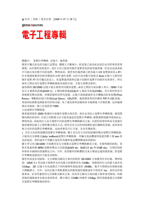
首頁| 登錄| 現在註冊 [2009年07月29日]關鍵字:電壓位準轉換記憶卡處理器隨著可攜式產品的功能日益豐富,體積又不斷縮小,耗電量已成為產品設計必須管理的重要課題。
由於製程技術進步,設計人員已能使用操作電壓更低的新型處理器,但這也造成系統中可能出現多種不同的電壓。
舉例來說,儘管某些處理器已將其最大I/O電壓限制為1.8V,許多週邊裝置卻仍採用傳統的3.3V操作電壓。
由於目前多數可卸除式flash記憶卡大都用於操作電壓3V的可攜式產品上,低電壓處理器和記憶卡的操作電壓不同情形也會發生,所以兩者之間必須以電壓位準轉換器做為連接介面,才能互相傳送資料。
處理器與SD/SDIO記憶卡過去都使用同樣的電壓,兩者之間的介面如圖1所示。
SDIO介面包含4個資料訊號(DA T0-3)、1個時脈訊號(CLK)和1個命令訊號(CMD),其中資料和命令訊號都是雙向訊號,時脈訊號則為單向訊號。
記憶卡連接器通常包含機械式防寫保護(Write Protect,WP)與記憶卡偵測(Card Detect,CD)開關,處理器會利用回傳的WP和CD訊號,來達到如啟動電路板某些控制功能。
為了避免資料訊號與命令線路進入浮動狀態,這些線路都必須連接一個上拉電阻到VDD。
主流電壓位準轉換器隨著處理器和SDIO週邊的介面操作電壓出現差異,現在必須加入電壓位準轉換器,確保開關切換的相容性。
目前已有數種方法可提供適當的電壓位準轉換,實際選擇視應用環境而定。
舉例來說,系統設計人員可選擇不同的電壓位準轉換解決方案,以便控制資料與命令訊號在處理器與記憶卡之間的雙向傳送方式:採用具有方向控制接腳的電位轉換收發器,或者使用無方向性的電壓位準轉換器。
這兩者都是可行方案,各有其優缺點。
1. 具有方向控制接腳的電壓位準轉換器:圖2是具有方向控制接腳的雙向電壓位準轉換器,又稱為完全緩衝式(fully buffered)電壓位準轉換器。
其輸出電晶體通常能提供數十個mA的直流電流,資料速率只受輸出電容性負載和電晶體開關速度的限制。
Binary 8X8 Matrix 开关器与分析器说明书

B-200-AVDMATRIX-8X8WELCOME TO THE BINARY™ BRAND OF PRODUCTSThis product is engineered to provide years of exceptional reliability. Binary™ is one of the most highly regarded brands available today. We appreciate your business and we stand committed to providing our customers with the highest degree of quality and service in the industry.IMPORTANT SAFETY INSTRUCTIONS1. Read and follow all instructions and warnings in this manual.Keep for future reference.2. Do not install near any heat sources such as radiators, heat registers, stovesor other apparatus (including amplifiers).3. Do not install the unit near water or where moisture is present.4. Clean with a dry cloth.5. Unplug this apparatus during lightning storms or when unused for longperiods of time.6. Protect the power cord from being walked on or pinched particularly at plug,convenience receptacles, and the point where it exits from the apparatus.7. Refer all servicing to qualified service personnel. Servicing is required when theapparatus has been damaged in any way, such as when the power-supply cord or plug is damaged, liquid has been spilled or objects have fallen into theapparatus, the apparatus has been exposed to rain or moisture, does notoperate normally, or has been dropped.8. To completely disconnect this equipment from the AC mains, disconnectthe power supply cord plug from the AC receptacle.CAUTION: To reduce the risk of electrical shock, inspect the premises carefully.Do not use the unit if proper equipment grounding cannot be verified.FEATURES• 8 inputs to 8 outputs True Matrix Switcher• Component Video (Y/Pb/Pr), Digital(PCM), Stereo Audio(L/R)• High Video Bandwidth (325 MB each path signal)• Supports all HDTV resolutions: 480i, 480p, 576i, 576p, 720p, 1080i, 1080p• Common channel Digital Audio (PCM) or Composite Video compliant• Compatible with all Component Video display devices• Controllable via IR or RS-232• Rack mount ears included• Power supply 12Volt DC, Switching 100~230VAC, 50/60Hz includedINTRODUCTIONThe B-200-AVDMATRIX-8X8 is a true Matrix Routing Switcher for Component Video,Digital Audio, and Stereo Audio signals. It provides 8 individual Component inputswith 8 individual Component outputs. This matrix router allows any component A/Vsource to be shown on any of the eight outputs independently or simultaneously.PACKAGE CONTENTS:• 8x8 Matrix Switcher• Owners Manual• IR Remote Controller• Rack mount ears (2U)• RS232 Cable• Power Supply 12V DC, 2AmpOPTIONAL ACCESSORIES:• B-RGBLR-350 - Cat-5 Balun for Component Video and Stereo Audio• B-RGBD-500 - Cat-5 Balun for Component Video and Digital Coax Audio • B-RGBIR-500 - Cat-5 Balun for Component Video and IR Flasher Pass Through • B-200-RGBDTOHD - Component and Digital Audio to HDMI Converter• Binary™ Audio/ Video Cables1. POWER ON SWITCH:The power switch turns the unit on and off into standby mode. The LED will illuminate blue to indicate that the switcher is ON and is receiving power.2. INPUT SOURCES STATUS:Auto scans source inputs 1-8 and will display a blue LED on front panel to indicate that a video source is on.3. OUTPUT SOURCES STATUS LED DISPLAY:Numbered LEDs for each output that illuminates blue to indicate that a video output is on and which source is selected.4. IR SENSOR:The IR sensor is located between the 4 and 5 output LEDs. This sensor receives IR commands from the remote controller.5. RACK MOUNT EARS (PAIR): Removable - 2U high (included)FRONT PANEL FEATURES6. A/V OUTPUTS:(8) Component Video (Y/Pb/Pr),(8) Digital Audio (PCM), Stereo Audio (L/R)7. A/V INPUTS:(8) Component Video (Y/Pb/Pr),(8) Digital Audio (PCM), Stereo Audio (L/R)8. RS-232 CONNECTIONSerial control port to allow for integration with control systems9. DC POWER:12 Volt DC power supply 2 amp (Included)REAR PANEL FEATURESINSTALLATION1. Connect the component A/V sources into the input connectors of the switcher.2. Connect the switchers A/V outputs directly to local displays or use any ofBinary’s™ extenders for remote displays.3. Power on the input sources.4. Connect the power supply into the switcher and turn on the display you want to watch.5. Use the IR remote to select the desired input source. An RS232 port is available for additional control when using third party integration systems.NOTE: IR commands will not send out a message on the serial port as status changes.When writing 2-way drivers, please pull the status regularly as to ensure the controlsystem accurately reflects the current settings. TROUBLESHOOTING1. No Video:• Ensure the power switch is on.• Confirm that the correct source is routed to the correct output.• Confirm that the source is powered on and connected to the correct input.• Confirm that the source is outputting a signal (using the Source Status LED)on the front of the unit.• Confirm the TV is on the correct input.2. Poor Video (hum bars in picture, picture distortion, noise in picture)• The #1 cause of poor video quality is low-quality interconnects. Never use theinterconnect cables that are included with DVD players, cable boxes, etc, as theyare very susceptible to EMI and noise. We highly recommend using Binary™ Cables, which are designed for this application.• Confirm that the source is outputting video at the correct levels. You can try to bypass the switcher and connect the display directly to the source and confirm the source is outputting a clean signal• Confirm that the connections between the TV and the switcher are good.• If using a Balun, confirm that the CAT-5 is terminated with TIA-568b standards onboth sides. You can also bypass the switcher by connecting the source directly tothe Balun to ensure the noise is not an interference issue with the CAT5 or the Balun.• Confirm that the power for the switcher and source gear is clean and is not sharing a circuit with noisy devices (ceiling fans, refrigerators, florescent lights, etc)• Some homes that do not have adequate grounding can have ground loops between different circuits. In these cases, you can try to use a ground lift at the TV to eliminate ground loop issues that can create noise in Video.IR REMOTE CONTROL1. DISCRETE POWER ON2. DISCRETE POWER OFF3. DESTINATION: OUTPUTS 1-84. SOURCE: INPUTS 1-8This remote provides discrete Power On and Off as well as discrete source selection. Switching commands must be sent in 2 strings (Output – Input). To make a selection:1. Be sure the unit is on by pushing the ON button2. Press the button for the desired output from DESTINATION choices 1-8.3. Press the button for the desired input, from SOURCE choices 1-8.Example:If you want to see Input 4 on Output 5, first press “5” in the DESTINATION section, then press “4” in the SOURCE section.TYPICAL APPLICATION8 Component sources to 8 Component Output Matrix Switcher(DVD Players and TV’s shown - a variety of components can be used including, but not limited to: Projectors, TVs, Blu-Ray Players, Cable boxes, Satellite, etc...)SPECIFICATIONSType of Switcher8 in to 8 out, Component Video-Digital-Audio Matrix SwitcherI/O Signals Component Video (YPbPr) 0.5~1.0Vpp, DDC 5Vpp,Digital Audio (PCM), Via 1x RCA connector Stereo Audio (L/R), Via 2x RCA connector(Red/white)Video Bandwidth325MHz(-3db), 200mVp-pVideo Supported480i/ 480p/ 576i/ 576p/ 720p/ 1080i/ 1080pAudio Supported Digital Audio (PCM) 110MB and Stereo Audio(L/R)Crosstalk-83 db@5MHzControls IR remote, RS232Gain control60MHz 0.1 db gain flatnessChassis Material MetalSafety Approvals CE, FCC, RoHS (2002/95/EC), ErP.Dimensions (LxWxH)19” x 7.87” x 3.46”Power Supply12VDC / 2A (consumption 1.6A Max) Switching 50/60Hz,100~230 VACShipping Weight 5.42 lb*Note: Specifications are subject to change without notice. Dimensions and weight are approximate.REGULATORY COMPLIANCEThis product complies with the relevant standards for CE, FCC and RoHS approval.The Power Adaptor/Supply has been tested for compliance with UL, CSA, and CE standards.WARRANTY2-Year Limited WarrantyThis Binary™ Product has a Two-Year Limited Warranty. This warranty includes parts and labor repairs on all components found to be defective in material or workmanship under normal conditions of use. This warranty shall not apply to products which have been abused, modified or disassembled. Products to be repaired under this warranty must be returned to SnapAV or a designated service center with prior notification and an assigned return authorization number (RA).。
- 1、下载文档前请自行甄别文档内容的完整性,平台不提供额外的编辑、内容补充、找答案等附加服务。
- 2、"仅部分预览"的文档,不可在线预览部分如存在完整性等问题,可反馈申请退款(可完整预览的文档不适用该条件!)。
- 3、如文档侵犯您的权益,请联系客服反馈,我们会尽快为您处理(人工客服工作时间:9:00-18:30)。
A inputs B inputs
Input clamp current Output clamp current Continuous output current
SCES643A – NOVEMBER 2006 – REVISED JANUARY 2007
TYPICAL OPERATING CIRCUIT
1.8 V
3.3 V
1.8 -V System Controller
Data
VCCA OE
VCCB
TXB0108
A1
B1
A2
B2
A3
B3
A4
B4
A5
B5
A6
FEATURES
• 1.2 V to 3.6 V on A Port and 1.65 to 5.5 V on B Port (VCCA ≤ VCCB)
• VCC Isolation Feature – If Either VCC Input Is at GND, All Outputs Are in the High-Impedance State
A1 1 VCCA 2
A2 3 A3 4 A4 5 A5 6 A6 7 A7 8
A8 9 OE 10
20 B1 19 VCCB 18 B2 17 B3 16 B4 15 B5 14 B6 13 B7
12 B8 11 GND
RGY PACKAGE (TOP VIEW)
B1
A1
1
VCCA 2 A2 3 A3 4 A4 5 A5 6 A6 7 A7 8 A8 9
Copyright © 2006–2007, Texas Instruments Incorporated
元器件交易网
TXB0108 8-BIT BIDIRECTIONAL VOLTAGE-LEVEL TRANSLATOR WITH AUTO-DIRECTION SENSING AND ±15-kV ESD PROTECTION
TA –40°C to 85°C
ORDERING INFORMATION
PACKAGE (1)
ORDERABLE PART NUMBER
QFN – RGY
Reel of 1000
TXB0108RGYR
TSSOP – PW
Reel of 2000
TXB0108PWR
VFBGA – GXY
Reel of 2500
4
A3
Input/output 3. Referenced to VCCA.
5
A4
Input/output 4. Referenced to VCCA.
6
A5
Input/output 5. Referenced to VCCA.
7
A6
Input/output 6. Referenced to VCCA.
• OE Input Circuit Referenced to VCCA • Low Power Consumption, 4-µA Max ICC • Ioff Supports Partial-Power-Down Mode
Operation
• Latch-Up Performance Exceeds 100 mA Per JESD 78, Class II
16
B4
Input/output 4. Referenced to VCCB.
17
B3
Input/output 3. Referenced to VCCB.
18
B2
Input/output 2. Referenced to VCCB.
19
VCCB
B-port supply voltage. 1.65 V ≤ VCCB ≤ 5.5 V.
B6
A7
B7
A8
B8
3.3-V System
Data
Absolute Maximum Ratings(1)
over operating free-air temperature range (unless otherwise noted)
VCCA VCCB VI VO VO IIK IOK IO
θJA
Tstg
Supply voltage range
Supply voltage range
Input voltage range(2)
Voltage range applied to any output in the high-impedance or power-off state(2)
Voltage range applied to any output in the high or low state(2)(3)
元器件交易网
TXB0108 8-BIT BIDIRECTIONAL VOLTAGE-LEVEL TRANSLATOR WITH AUTO-DIRECTION SENSING AND ±15-kV ESD PROTECTION
SCES643A – NOVEMBER 2006 – REVISED JANUARY 2007
When the output-enable (OE) input is low, all outputs are placed in the high-impedance state.
The TXB0101 is desinged so that the OE input circuit is supplied by VCCA.
SCES643A – NOVEMBER 2006 – REVISED JANUARY 2007
DESCRIPTION/ORDERING INFORMATION (CONTINUED)
This device is fully specified for partial-power-down applications using Ioff. The Ioff circuitry disables the outputs, preventing damaging current backflow through the device when it is powered down.
GXY OR ZXY PACKAGE (BOTTOM VIEW) 1 2 3 45
D C B A
TERMINAL ASSIGNMENTS (20-Ball GXY/ZXY Package)
1
2
3
4
5
D
VCCB
B2
B4
B6
B8
C
B1
B3
B5
B7
GND
B
A1
A3
A5
A7
OE
A
VCCA
A2
A4
A6
A8
PW PACKAGE (TOP VIEW)
20
B1
Input/output 1. Referenced to VCCB.
2
Submit Documentation Feedback
元器件交易网
TXB0108 8-BIT BIDIRECTIONAL VOLTAGE-LEVEL TRANSLATOR WITH AUTO-DIRECTION SENSING AND ±15-kV ESD PROTECTION
10
20 19 VCCB 18 B2 17 B3 16 B4 15 B5 14 B6 13 B7 12 B8
11
GND
OE
DESCRIPTION/ORDERING INFORMATION
This 8-bit noninverting translator uses two separate configurable power-supply rails. The A port is designed to track VCCA. VCCA accepts any supply voltage from 1.2 V to 3.6 V. The B port is designed to track VCCB. VCCB accepts any supply voltage from 1.65 V to 5.5 V. This allows for universal low-voltage bidirectional translation between any of the 1.2-V, 1.5-V, 1.8-V, 2.5-V, 3.3-V, and 5-V voltage nodes. VCCA should not exceed VCCB.
PRODUCTION DATA information is current as of publication date. Products conform to specifications per the terms of the Texas Instruments standard warranty. Production processing does not necessarily include testing of all parameters.
TXB0108GXYR
VFBGA – ZXY (Pb-free) Reel of 2500
TXB0108ZXYR
TOP-SIDE MARKING YE08 YE08 YE08 ings, standard packing quantities, thermal data, symbolization, and PCB design guidelines are available at /sc/package.
To ensure the high-impedance state during power up or power down, OE should be tied to GND through a pulldown resistor; the minimum value of the resistor is determined by the current-sourcing capability of the driver.