Analysis of one particle excitations in phenomenological models of QCD
The Problem of Modelling of Economic Dynamics in Differential Form

3 Constructive arguments 23 3.1 Leontief’s differential model . . . . . . . . . . . . . . . . . . . . . 23 3.2 Nonlinear model and an alternative . . . . . . . . . . . . . . . . . 25 3.3 Representativeness of the integral model . . . . . . . . . . . . . . 28
1
Introduction
The authors have tried to analyze procedures of the construction of differential equations that are employed for modeling of macroeconomic processes. The results prove to be rather unexpected. Thus, the derivation of the differential equation of Harrod’s model is based on a linear relation between capital and income. As a result, there arises a contradiction in terms of dimension that is rooted in incorrect treatment of the fundamental notion of the infinitesimal quantity. One can overcome this contradiction by relating capital to the integral of income over a corresponding time interval. However, in this case, the solution is by no means an exponential growth but a much more realistic relation that reflects, in particular, objective finiteness of the prognostic period. An analysis of the models of Harrod-Domar, Phillips, as well as of other models (see the well-known treatise by R. Allen), leads us to the conclusion that analogous deficiencies are, in principle, inherent in these models too. In general, the refraction in the sphere of economic dynamics of the methodology of the construction of mathematical models borrowed from the field of natural sciences, such as dynamics, electrodynamics, etc., proves to be absolutely unjustified. As a matter of fact, differential equations adequate to these models follow naturally from the consideration of an infinitesimal element. However, as regards the problems of economics, such an approach is objectively senseless. Nevertheless, economics, in its turn, has intrinsic advantages from the point of view of possibilities of mathematical modeling, which is embodied in the notion of balance. As we will show, there exist formal means to reduce Leontief’s model of ”expenses-output” in its canonical interpretation to a system of linear differential equation (of, generally speaking, arbitrary order with respect to the derivatives). At the same time, the scantiness of the arsenal of the means of linear theory that are used in representative modeling of macroeconomic processes is almost universally recognized nowadays. In this regard, we will characterize briefly those areas of systems analysis that are devoted to the construction of nonlinear models that are adequate to a given ”input-output” mapping. In what follows, we nonetheless note that Leontief’s model in the differential form can be elementary reduced to a Fredholm integral equation of the second kind (with respect to a vector function), whose theory and algorithms of numerical realization are as constructive as possible. In the case, when the kernel of such an equation depends on a parameter, which is quite naturally interpreted in terms of the object sphere, the spectrum of its possible solutions becomes extremely wide. We think that the development of the theory of Fredholm integral equations of the second kind, whose kernels contain parameters, and its application to the modeling of the processes of economic dynamics is rather promising. Note on literature references in the English version: The reader should be advised that all the references to page and section numbers appearing in the text are given according to the Russian editions of corresponding literature sources. Contact address : voronin@.ua
有关量子力学的英语作文
有关量子力学的英语作文Quantum mechanics, a fundamental theory in physics, has been a subject of fascination and debate since its inception in the early 20th century. It describes the behavior of matter and energy at the smallest scales, where the classical laws of physics no longer apply. This essay aims to explore the key principles of quantum mechanics, its implications for our understanding of the universe, and the ongoing challenges it presents to scientists and philosophers alike.Firstly, the concept of wave-particle duality is central to quantum mechanics. This principle posits that all particles, such as electrons, can exhibit both wave-like and particle-like properties. This duality is demonstrated in the famous double-slit experiment, where particles create aninterference pattern when not observed, but act as discrete entities when measured. The act of observation, therefore, plays a critical role in determining the state of a quantum system.Secondly, the superposition principle is another cornerstone of quantum mechanics. It states that a quantum system can exist in multiple states simultaneously until it is measured. This is exemplified by the thought experiment known asSchrödinger's cat, where a cat in a sealed box is considered to be both alive and dead until the box is opened and thecat's state is observed.Entanglement, a phenomenon where particles become interconnected and the state of one instantaneously influences the state of another, regardless of the distance between them, is another intriguing aspect of quantum mechanics. This has led to the development of quantum computing, which promises to revolutionize information processing by performing calculations at speeds unattainable by classical computers.However, quantum mechanics also presents significant challenges. The interpretation of quantum theory is a subject of ongoing debate. The Copenhagen interpretation suggeststhat the act of measurement collapses the wave function, determining the outcome, while the many-worlds interpretation proposes that all possible outcomes of a quantum event exist in separate, non-interacting parallel universes.Moreover, the reconciliation of quantum mechanics with general relativity, the theory of gravity, remains an unsolved problem in physics. The two theories operate under fundamentally different principles, and finding a unified theory that encompasses both has been a holy grail for physicists.In conclusion, quantum mechanics has reshaped our understanding of the microscopic world and has profound implications for technology, philosophy, and the very fabric of reality. As research continues, it is likely that the mysteries of quantum mechanics will continue to inspire awe and provoke thought about the nature of existence itself.。
An Analysis of States in the Phase Space From Quantum Mechanics to General Relativity
1
ABSTRACT The paper has euristic character. It exploits basic concepts of quantum physics to infer on a selfconsistent basis the properties of the gravitational field. The only assumption of the theoretical model is the quantum uncertainty: the physical properties of quantum systems depends on the delocalization ranges of the constituent particles and not on their local dynamical variables. The conceptual approach follows the same formalism already described in early non-relativistic papers [S. Tosto, Il Nuovo Cimento B, vol. 111, n.2, (1996) and S. Tosto, Il Nuovo Cimento D, vol. 18, n.12, (1996)]. The paper shows that the extended concept of space time uncertainty is inherently consistent with the postulates of special relativity and that the most significant results of general relativity are achieved as straightforward consequence of the space time delocalization of quantum particles.
Singularity of the density of states in the two-dimensional Hubbard model from finite size
a r X i v :c o n d -m a t /9503139v 1 27 M a r 1995Singularity of the density of states in the two-dimensional Hubbard model from finitesize scaling of Yang-Lee zerosE.Abraham 1,I.M.Barbour 2,P.H.Cullen 1,E.G.Klepfish 3,E.R.Pike 3and Sarben Sarkar 31Department of Physics,Heriot-Watt University,Edinburgh EH144AS,UK 2Department of Physics,University of Glasgow,Glasgow G128QQ,UK 3Department of Physics,King’s College London,London WC2R 2LS,UK(February 6,2008)A finite size scaling is applied to the Yang-Lee zeros of the grand canonical partition function for the 2-D Hubbard model in the complex chemical potential plane.The logarithmic scaling of the imaginary part of the zeros with the system size indicates a singular dependence of the carrier density on the chemical potential.Our analysis points to a second-order phase transition with critical exponent 12±1transition controlled by the chemical potential.As in order-disorder transitions,one would expect a symmetry breaking signalled by an order parameter.In this model,the particle-hole symmetry is broken by introducing an “external field”which causes the particle density to be-come non-zero.Furthermore,the possibility of the free energy having a singularity at some finite value of the chemical potential is not excluded:in fact it can be a transition indicated by a divergence of the correlation length.A singularity of the free energy at finite “exter-nal field”was found in finite-temperature lattice QCD by using theYang-Leeanalysisforthechiral phase tran-sition [14].A possible scenario for such a transition at finite chemical potential,is one in which the particle den-sity consists of two components derived from the regular and singular parts of the free energy.Since we are dealing with a grand canonical ensemble,the particle number can be calculated for a given chem-ical potential as opposed to constraining the chemical potential by a fixed particle number.Hence the chem-ical potential can be thought of as an external field for exploring the behaviour of the free energy.From the mi-croscopic point of view,the critical values of the chemical potential are associated with singularities of the density of states.Transitions related to the singularity of the density of states are known as Lifshitz transitions [15].In metals these transitions only take place at zero tem-perature,while at finite temperatures the singularities are rounded.However,for a small ratio of temperature to the deviation from the critical values of the chemical potential,the singularity can be traced even at finite tem-perature.Lifshitz transitions may result from topological changes of the Fermi surface,and may occur inside the Brillouin zone as well as on its boundaries [16].In the case of strongly correlated electron systems the shape of the Fermi surface is indeed affected,which in turn may lead to an extension of the Lifshitz-type singularities into the finite-temperature regime.In relating the macroscopic quantity of the carrier den-sity to the density of quasiparticle states,we assumed the validity of a single particle excitation picture.Whether strong correlations completely distort this description is beyond the scope of the current study.However,the iden-tification of the criticality using the Yang-Lee analysis,remains valid even if collective excitations prevail.The paper is organised as follows.In Section 2we out-line the essentials of the computational technique used to simulate the grand canonical partition function and present its expansion as a polynomial in the fugacity vari-able.In Section 3we present the Yang-Lee zeros of the partition function calculated on 62–102lattices and high-light their qualitative differences from the 42lattice.In Section 4we analyse the finite size scaling of the Yang-Lee zeros and compare it to the real-space renormaliza-tion group prediction for a second-order phase transition.Finally,in Section 5we present a summary of our resultsand an outlook for future work.II.SIMULATION ALGORITHM AND FUGACITY EXPANSION OF THE GRAND CANONICALPARTITION FUNCTIONThe model we are studying in this work is a two-dimensional single-band Hubbard HamiltonianˆH=−t <i,j>,σc †i,σc j,σ+U i n i +−12 −µi(n i ++n i −)(1)where the i,j denote the nearest neighbour spatial lat-tice sites,σis the spin degree of freedom and n iσis theelectron number operator c †iσc iσ.The constants t and U correspond to the hopping parameter and the on-site Coulomb repulsion respectively.The chemical potential µis introduced such that µ=0corresponds to half-filling,i.e.the actual chemical potential is shifted from µto µ−U412.(5)This transformation enables one to integrate out the fermionic degrees of freedom and the resulting partition function is written as an ensemble average of a product of two determinantsZ ={s i,l =±1}˜z = {s i,l =±1}det(M +)det(M −)(6)such thatM ±=I +P ± =I +n τ l =1B ±l(7)where the matrices B ±l are defined asB ±l =e −(±dtV )e −dtK e dtµ(8)with V ij =δij s i,l and K ij =1if i,j are nearestneigh-boursand Kij=0otherwise.The matrices in (7)and (8)are of size (n x n y )×(n x n y ),corresponding to the spatial size of the lattice.The expectation value of a physical observable at chemical potential µ,<O >µ,is given by<O >µ=O ˜z (µ){s i,l =±1}˜z (µ,{s i,l })(9)where the sum over the configurations of Ising fields isdenoted by an integral.Since ˜z (µ)is not positive definite for Re(µ)=0we weight the ensemble of configurations by the absolute value of ˜z (µ)at some µ=µ0.Thus<O >µ= O ˜z (µ)˜z (µ)|˜z (µ0)|µ0|˜z (µ0)|µ0(10)The partition function Z (µ)is given byZ (µ)∝˜z (µ)N c˜z (µ0)|˜z (µ0)|×e µβ+e −µβ−e µ0β−e −µ0βn (16)When the average sign is near unity,it is safe to as-sume that the lattice configurations reflect accurately thequantum degrees of freedom.Following Blankenbecler et al.[1]the diagonal matrix elements of the equal-time Green’s operator G ±=(I +P ±)−1accurately describe the fermion density on a given configuration.In this regime the adiabatic approximation,which is the basis of the finite-temperature algorithm,is valid.The situa-tion differs strongly when the average sign becomes small.We are in this case sampling positive and negative ˜z (µ0)configurations with almost equal probability since the ac-ceptance criterion depends only on the absolute value of ˜z (µ0).In the simulations of the HSfields the situation is dif-ferent from the case of fermions interacting with dynam-ical bosonfields presented in Ref.[1].The auxilary HS fields do not have a kinetic energy term in the bosonic action which would suppress their rapidfluctuations and hence recover the adiabaticity.From the previous sim-ulations on a42lattice[3]we know that avoiding the sign problem,by updating at half-filling,results in high uncontrolledfluctuations of the expansion coefficients for the statistical weight,thus severely limiting the range of validity of the expansion.It is therefore important to obtain the partition function for the widest range ofµ0 and observe the persistence of the hierarchy of the ex-pansion coefficients of Z.An error analysis is required to establish the Gaussian distribution of the simulated observables.We present in the following section results of the bootstrap analysis[17]performed on our data for several values ofµ0.III.TEMPERATURE AND LATTICE-SIZEDEPENDENCE OF THE YANG-LEE ZEROS The simulations were performed in the intermediate on-site repulsion regime U=4t forβ=5,6,7.5on lat-tices42,62,82and forβ=5,6on a102lattice.The ex-pansion coefficients given by eqn.(14)are obtained with relatively small errors and exhibit clear Gaussian distri-bution over the ensemble.This behaviour was recorded for a wide range ofµ0which makes our simulations reli-able in spite of the sign problem.In Fig.1(a-c)we present typical distributions of thefirst coefficients correspond-ing to n=1−7in eqn.(14)(normalized with respect to the zeroth power coefficient)forβ=5−7.5for differ-entµ0.The coefficients are obtained using the bootstrap method on over10000configurations forβ=5increasing to over30000forβ=7.5.In spite of different values of the average sign in these simulations,the coefficients of the expansion(16)indicate good correspondence between coefficients obtained with different values of the update chemical potentialµ0:the normalized coefficients taken from differentµ0values and equal power of the expansion variable correspond within the statistical error estimated using the bootstrap analysis.(To compare these coeffi-cients we had to shift the expansion by2coshµ0β.)We also performed a bootstrap analysis of the zeros in theµplane which shows clear Gaussian distribution of their real and imaginary parts(see Fig.2).In addition, we observe overlapping results(i.e.same zeros)obtained with different values ofµ0.The distribution of Yang-Lee zeros in the complexµ-plane is presented in Fig.3(a-c)for the zeros nearest to the real axis.We observe a gradual decrease of the imaginary part as the lattice size increases.The quantitative analysis of this behaviour is discussed in the next section.The critical domain can be identified by the behaviour of the density of Yang-Lee zeros’in the positive half-plane of the fugacity.We expect tofind that this density is tem-perature and volume dependent as the system approaches the phase transition.If the temperature is much higher than the critical temperature,the zeros stay far from the positive real axis as it happens in the high-temperature limit of the one-dimensional Ising model(T c=0)in which,forβ=0,the points of singularity of the free energy lie at fugacity value−1.As the temperature de-creases we expect the zeros to migrate to the positive half-plane with their density,in this region,increasing with the system’s volume.Figures4(a-c)show the number N(θ)of zeros in the sector(0,θ)as a function of the angleθ.The zeros shown in thesefigures are those presented in Fig.3(a-c)in the chemical potential plane with other zeros lying further from the positive real half-axis added in.We included only the zeros having absolute value less than one which we are able to do because if y i is a zero in the fugacity plane,so is1/y i.The errors are shown where they were estimated using the bootstrap analysis(see Fig.2).Forβ=5,even for the largest simulated lattice102, all the zeros are in the negative half-plane.We notice a gradual movement of the pattern of the zeros towards the smallerθvalues with an increasing density of the zeros nearθ=πIV.FINITE SIZE SCALING AND THESINGULARITY OF THE DENSITY OF STATESAs a starting point for thefinite size analysis of theYang-Lee singularities we recall the scaling hypothesis forthe partition function singularities in the critical domain[11].Following this hypothesis,for a change of scale ofthe linear dimension LLL→−1),˜µ=(1−µT cδ(23)Following the real-space renormalization group treatmentof Ref.[11]and assuming that the change of scaleλisa continuous parameter,the exponentαθis related tothe critical exponentνof the correlation length asαθ=1ξ(θλ)=ξ(θ)αθwe obtain ξ∼|θ|−1|θ|ναµ)(26)where θλhas been scaled to ±1and ˜µλexpressed in terms of ˜µand θ.Differentiating this equation with respect to ˜µyields:<n >sing =(−θ)ν(d −αµ)∂F sing (X,Y )ν(d −αµ)singinto the ar-gument Y =˜µαµ(28)which defines the critical exponent 1αµin terms of the scaling exponent αµof the Yang-Lee zeros.Fig.5presents the scaling of the imaginary part of the µzeros for different values of the temperature.The linear regression slope of the logarithm of the imaginary part of the zeros plotted against the logarithm of the inverse lin-ear dimension of the simulation volume,increases when the temperature decreases from β=5to β=6.The re-sults of β=7.5correspond to αµ=1.3within the errors of the zeros as the simulation volume increases from 62to 82.As it is seen from Fig.3,we can trace zeros with similar real part (Re (µ1)≈0.7which is also consistentwith the critical value of the chemical potential given in Ref.[22])as the lattice size increases,which allows us to examine only the scaling of the imaginary part.Table 1presents the values of αµand 1αµδ0.5±0.0560.5±0.21.3±0.3∂µ,as a function ofthe chemical potential on an 82lattice.The location of the peaks of the susceptibility,rounded by the finite size effects,is in good agreement with the distribution of the real part of the Yang-Lee zeros in the complex µ-plane (see Fig.3)which is particularly evident in the β=7.5simulations (Fig.4(c)).The contribution of each zero to the susceptibility can be singled out by expressing the free energy as:F =2n x n yi =1(y −y i )(29)where y is the fugacity variable and y i is the correspond-ing zero of the partition function.The dotted lines on these plots correspond to the contribution of the nearby zeros while the full polynomial contribution is given by the solid lines.We see that the developing singularities are indeed governed by the zeros closest to the real axis.The sharpening of the singularity as the temperature de-creases is also in accordance with the dependence of the distribution of the zeros on the temperature.The singularities of the free energy and its derivative with respect to the chemical potential,can be related to the quasiparticle density of states.To do this we assume that single particle excitations accurately represent the spectrum of the system.The relationship between the average particle density and the density of states ρ(ω)is given by<n >=∞dω1dµ=ρsing (µ)∝1δ−1(32)and hence the rate of divergence of the density of states.As in the case of Lifshitz transitions the singularity of the particle number is rounded at finite temperature.However,for sufficiently low temperatures,the singular-ity of the density of states remains manifest in the free energy,the average particle density,and particle suscep-tibility [15].The regular part of the density of states does not contribute to the criticality,so we can concentrate on the singular part only.Consider a behaviour of the typedensity of states diverging as the−1ρsing(ω)∝(ω−µc)1δ.(33)with the valueδfor the particle number governed by thedivergence of the density of states(at low temperatures)in spite of thefinite-temperature rounding of the singu-larity itself.This rounding of the singularity is indeedreflected in the difference between the values ofαµatβ=5andβ=6.V.DISCUSSION AND OUTLOOKWe note that in ourfinite size scaling analysis we donot include logarithmic corrections.In particular,thesecorrections may prove significant when taking into ac-count the fact that we are dealing with a two-dimensionalsystem in which the pattern of the phase transition islikely to be of Kosterlitz-Thouless type[23].The loga-rithmic corrections to the scaling laws have been provenessential in a recent work of Kenna and Irving[24].In-clusion of these corrections would allow us to obtain thecritical exponents with higher accuracy.However,suchanalysis would require simulations on even larger lattices.The linearfits for the logarithmic scaling and the criti-cal exponents obtained,are to be viewed as approximatevalues reflecting the general behaviour of the Yang-Leezeros as the temperature and lattice size are varied.Al-though the bootstrap analysis provided us with accurateestimates of the statistical error on the values of the ex-pansion coefficients and the Yang-Lee zeros,the smallnumber of zeros obtained with sufficient accuracy doesnot allow us to claim higher precision for the critical ex-ponents on the basis of more elaboratefittings of the scal-ing behaviour.Thefinite-size effects may still be signifi-cant,especially as the simulation temperature decreases,thus affecting the scaling of the Yang-Lee zeros with thesystem rger lattice simulations will therefore berequired for an accurate evaluation of the critical expo-nent for the particle density and the density of states.Nevertheless,the onset of a singularity atfinite temper-ature,and its persistence as the lattice size increases,areevident.The estimate of the critical exponent for the diver-gence rate of the density of states of the quasiparticleexcitation spectrum is particularly relevant to the highT c superconductivity scenario based on the van Hove sin-gularities[25],[26],[27].It is emphasized in Ref.[25]thatthe logarithmic singularity of a two-dimensional electrongas can,due to electronic correlations,turn into a power-law divergence resulting in an extended saddle point atthe lattice momenta(π,0)and(0,π).In the case of the14.I.M.Barbour,A.J.Bell and E.G.Klepfish,Nucl.Phys.B389,285(1993).15.I.M.Lifshitz,JETP38,1569(1960).16.A.A.Abrikosov,Fundamentals of the Theory ofMetals North-Holland(1988).17.P.Hall,The Bootstrap and Edgeworth expansion,Springer(1992).18.S.R.White et al.,Phys.Rev.B40,506(1989).19.J.E.Hirsch,Phys.Rev.B28,4059(1983).20.M.Suzuki,Prog.Theor.Phys.56,1454(1976).21.A.Moreo, D.Scalapino and E.Dagotto,Phys.Rev.B43,11442(1991).22.N.Furukawa and M.Imada,J.Phys.Soc.Japan61,3331(1992).23.J.Kosterlitz and D.Thouless,J.Phys.C6,1181(1973);J.Kosterlitz,J.Phys.C7,1046(1974).24.R.Kenna and A.C.Irving,unpublished.25.K.Gofron et al.,Phys.Rev.Lett.73,3302(1994).26.D.M.Newns,P.C.Pattnaik and C.C.Tsuei,Phys.Rev.B43,3075(1991);D.M.Newns et al.,Phys.Rev.Lett.24,1264(1992);D.M.Newns et al.,Phys.Rev.Lett.73,1264(1994).27.E.Dagotto,A.Nazarenko and A.Moreo,Phys.Rev.Lett.74,310(1995).28.A.A.Abrikosov,J.C.Campuzano and K.Gofron,Physica(Amsterdam)214C,73(1993).29.D.S.Dessau et al.,Phys.Rev.Lett.71,2781(1993);D.M.King et al.,Phys.Rev.Lett.73,3298(1994);P.Aebi et al.,Phys.Rev.Lett.72,2757(1994).30.E.Dagotto, A.Nazarenko and M.Boninsegni,Phys.Rev.Lett.73,728(1994).31.N.Bulut,D.J.Scalapino and S.R.White,Phys.Rev.Lett.73,748(1994).32.S.R.White,Phys.Rev.B44,4670(1991);M.Veki´c and S.R.White,Phys.Rev.B47,1160 (1993).33.C.E.Creffield,E.G.Klepfish,E.R.Pike and SarbenSarkar,unpublished.Figure CaptionsFigure1Bootstrap distribution of normalized coefficients for ex-pansion(14)at different update chemical potentialµ0for an82lattice.The corresponding power of expansion is indicated in the topfigure.(a)β=5,(b)β=6,(c)β=7.5.Figure2Bootstrap distributions for the Yang-Lee zeros in the complexµplane closest to the real axis.(a)102lat-tice atβ=5,(b)102lattice atβ=6,(c)82lattice at β=7.5.Figure3Yang-Lee zeros in the complexµplane closest to the real axis.(a)β=5,(b)β=6,(c)β=7.5.The correspond-ing lattice size is shown in the top right-hand corner. Figure4Angular distribution of the Yang-Lee zeros in the com-plex fugacity plane Error bars are drawn where esti-mated.(a)β=5,(b)β=6,(c)β=7.5.Figure5Scaling of the imaginary part ofµ1(Re(µ1)≈=0.7)as a function of lattice size.αm u indicates the thefit of the logarithmic scaling.Figure6Electronic susceptibility as a function of chemical poten-tial for an82lattice.The solid line represents the con-tribution of all the2n x n y zeros and the dotted line the contribution of the six zeros nearest to the real-µaxis.(a)β=5,(b)β=6,(c)β=7.5.。
去年材料物理答案整理
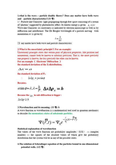
1.what is the wave – particle duality theory? Does any matter have both wave and particle characteristics?(33号)1)Particle-like Character: light propagating through free space consisting of a stream of …photons‟ suggested by photoelectric effect. Its kin etic energy is given: Wave-like Character: its correctness is indicated by electron microscope as well as by diffraction and interference. The De Broglie wavelength of a particle moving with momentum mv is given by:2)any matter have both wave and particle characteristics2.What is the uncertainty principle?( For an example)Uncertainty principle states that certain pairs of physical properties, like position and momentum, cannot both be known to arbitrary precision. That is, the more precisely one property is known, the less precisely the other can be known.For an example ( Electrons' Diffraction )the standard deviation of the X-distribution :a x =∆the standard deviation of P :Because :ph a ==λλϕ,sin ,h p x x =∆∆ Because the in sub diffraction is bigger :h p x ≥∆∆3.Wavefunction and its meaning. (33号)λA wave function or wavefunction is a mathematical tool used in quantum mechanics to describe the momentary states of subatomic particles .)(0),(r P Et i e t r ⋅--ψ=ψStatistical explanation of wavefunctionThe values of the wave function are probability amplitudes (振幅) — complex numbers — the squares of the absolute values of which give the probability distribution that the system will be in any of the possible states.4.The solution of Schrodinger equation of the particles bound in one-dimensional potential wells. (1/2号)νεh k =mvh =λϕsin pa p x x =∆∆∴x p ∆Single particle in one dimensions :Free particle ti x m ∂∂∂∂ψ=ψ- 2222 Time dependent5,What is the best obvious characteristics of crystal lattice ? (3/4号)The best obvious characteristics of crystal lattice is that atoms are arranged periodically in crystal lattic e.A crystal or crystalline solid is a solid material, whose constituent atoms, molecules, or ions are arranged in an orderly repeating pattern extending in all three spatial dimensions.6.what is the forbidden band, empty band, valence band ,conduction band? (5/6号)● allowed band: the energy band which allow to be occupied by electron● forbidden band: the region between allow band, in which electron is not allowedto occupy● empty band: the energy band in which electron cannot be found in each level ● valence band: the energy band corresponding to valence electron● conduction band: above Valence band the allow band which have the lowestenergye the theory of energy band to explain what is the insulator, semiconductor and conductor.Solution :As is shown in the above picture , in metal the highest energy band filled by electrons is not full ,furthermore ,the density of electron in the energy band is v ery high , it has the same magnitude as the density of the atom, so the conductivity of metal is very high.In the case of insulator, there is an energy gap , a finite excitation energy is required to carry the electrons up over the gap into the next band . This can‟t be supplied by small constant electric field, then the conductivity is very low ,almost zero.As for semiconductor, the energy gap is small . At the temperature T there will be a small , but not zero, density of electrons excited by thermal fluctuations into the upper band. These electrons can easily carry a current, which would increase rapidly at higher temperature.8,What is the mobility of semiconductor? What are the factors which have effect on the mobility? (第4个ppt, 33-36页)(9/10号)Answer: It is the average drift velocity of carrier in unit electric field.assume the semiconductor is n-type semiconductor, electron concentration is n 0, the average drift velocity of electrons is v d .we know the current density ( J ) is :d d n qv n sqsv n s I J 00=== According to the ohm‟s law,E J n n σ= We can getn d n q n E v q n μσ00== , Ev d n =μ , it is the electron mobility Similarily p p q p μσ0= , p μis the hole mobilitySo in the actual semiconductor,p n q p q n μμσ00+=But in n-type semiconductor, n 0 >> p 0n q n μσ0=In p-type semiconductor, p 0 >> n 0p q p μσ0=In intrinsic semiconductor, n 0=p 0)(0p n q n μμσ+=载流子迁移率的影响因素很多,关于这方面比较系统的信息没有找到,但老师强调了一点,随着半导体中掺杂浓度的升高,其载流子的迁移率降低。
振动疲劳介绍

Introduction
Traditionally fatigue damage is associated with time dependent loading, in the form of local stress or strain histories. However there often are situations where these loading time signals can not easily be determined. As examples one can think of shaker tables, or signals like the wind load on a wind mill where just the length of necessary measurements enforces to use other representations of the loads. In these cases power spectral densities define the loads.
The post-processing features are especially adapted to the given applications and they are not only intended to really fast identify the critical regions but give answers to how to solve the durability problems. Due to the efficient solving and the tight integration multiple designs can be analyzed without big manual interaction to reach the design that fulfills both weight and durability requirements.
First-principle study of excitonic self-trapping in diamond
a rXiv:mtrl -th/9522v14Fe b1995First-principle study of excitonic self-trapping in diamond Francesco Mauri ∗and Roberto Car Institut Romand de Recherche Num´e rique en Physique des Mat´e riaux (IRRMA)IN-Ecublens 1015Lausanne,Switzerland Abstract We present a first-principles study of excitonic self-trapping in diamond.Our calculation provides evidence for self-trapping of the 1s core exciton and gives a coherent interpretation of recent experimental X-ray absorption and emission data.Self-trapping does not occur in the case of a single valence exciton.We predict,however,that self-trapping should occur in the case of a valence biexciton.This process is accompanied by a large local relaxation of the lattice which could be observed experimentally.PACS numbers:61.80.−x,71.38.+i,71.35+z,71.55.−iTypeset using REVT E XDiamond presents an unusually favorable combination of characteristics that,in connection with the recent development of techniques for the deposition of thin diamondfilms,make this material a good candidate for many technological applications.Particularly appealing is the use of diamond in electronic or in opto-electronic devices,as e.g.UV-light emitting devices.Moreover,diamond is an ideal material for the construction of windows that operate under high power laser radiation or/and in adverse environments.It is therefore interesting to study radiation induced defects with deep electronic levels in the gap,since these can have important implications in many of these applications.Excitonic self-trapping is a possible mechanism for the formation of deep levels in the gap.The study of such processes in a purely covalent material,like diamond,is interesting also from a fundamental point of view.Indeed,excitonic self-trapping has been studied so far mostly in the context of ionic compounds,where it is always associated with,and often driven by,charge transfer effects.In a covalent material the driving mechanism for self-trapping is instead related to the difference in the bonding character between the valence and the conduction band states.Both experimental data and theoretical arguments suggest the occurrence of self-trapping processes in diamond.In particular,a nitrogen(N)substitutional impurity induces a strong local deformation of the lattice[1–3]that can be interpreted as a self-trapping of the donor electron.The structure of a1s core exciton is more controversial[4–9].Indeed the similarity between an excited core of carbon and a ground-state core of nitrogen suggests that the core exciton should behave like a N impurity.However,the position of the core exciton peak in the diamond K-edge absorption spectra is only0.2eV lower than the conduction band minimum[4,7,8],while a N impurity originates a deep level1.7eV below the conduction band edge[10].On the other hand,emission spectra[8]suggest that a1s core exciton should self-trap like a N impurity.Finally,we consider valence excitations.In this case experimental evidence indicates that a single valence exciton is of the Wannier type,i.e.there is no self-trapping.To our knowledge,neither experimental nor theoretical investigations on the behavior of a valence biexciton in diamond have been performed,although simple scalingarguments suggest that the tendency to self-trap should be stronger for biexcitons than for single excitons.In this letter,we present a detailed theoretical study of excitonic self-trapping effects in diamond.In particular,we have investigated the Born-Oppenheimer(BO)potential energy surfaces corresponding to a core exciton,a valence exciton and a valence biexciton in the context of density functional theory(DFT),within the local density approximation(LDA) for exchange and correlation.Our calculation indicates that the1s core exciton is on a different BO surface in absorption and in emission experiments.Indeed X-ray absorption creates excitons in a p-like state as required by dipole selection rules.Subsequently the system makes a transition to an s-like state associated to a self-trapping distortion of the atomic lattice,similar to that found in the N impurity case.These results provide a coherent interpretation of the experimental data.In addition,our calculation suggests that self-trapping should also occur for a valence biexciton.This is a prediction that could be verified experimentally.Let us start by discussing a simple model[11,12].In diamond,the occupied valence and the lower conduction band states derive from superpositions of atomic sp3hybrids having bonding and antibonding character,respectively.Thus,when an electron,or a hole,or an electron-hole pair is added to the system,this can gain in deformation energy by relaxing the atomic lattice.Scaling arguments suggest that the deformation energy gain E def∝−1/N b, where N b is the number of bonds over which the perturbation is localized.This localization,due to quantum confinement.The in turn,has a kinetic energy cost E kin∝+1/N2/3bbehavior of the system is then governed by the value of N b that minimizes the total energy E sum=E def+E kin.Since the only stationary point of E sum is a maximum,E sum attains its minimum value at either one of the two extrema N b=1or N b=∞.If the minimum occurs for N b=1,the perturbation is self-trapped on a single bond which is therefore stretched.If the minimum occurs for N b=∞,there is no self-trapping and the perturbation is delocalized.When N p particles(quasi-particles)are added to the system,one can showthat,for a given N b,E def scales as N2p,while E kin scales as N p.As a consequence,the probability of self-trapping is enhanced when N p is larger.This suggests that biexcitons should have a stronger tendency to self-trap than single excitons[12,13].In order to get a more quantitative understanding of self-trapping phenomena in dia-mond,we performed self-consistent electronic structure calculations,using norm-conserving pseudopotentials[14]to describe core-valence interactions.The wave-functions and the electronic density were expanded in plane-waves with a cutoffof35and of140Ry,respec-tively.We used a periodically repeated simple cubic supercell containing64atoms at the experimental equilibrium lattice constant.Only the wave-functions at theΓpoint were con-sidered.Since the self-trapped states are almost completely localized on one bond,they are only weakly affected by the boundary conditions in a64atom supercell.The effect of the k-point sampling was analysed in Ref.[3]where similar calculations for a N impurity were performed using the same supercell.It was found that a more accurate k-point sampling does not change the qualitative physics of the distortion but only increases the self-trapping energy by20%compared to calculations based on theΓ-point only[3].In order to describe a core exciton we adopted the method of Ref.[15],i.e.we generated a norm conserving pseudopotential for an excited carbon atom with one electron in the1s core level andfive electrons in the valence2s-2p levels.In our calculations for a valence exciton or biexciton we promoted one or two electrons,respectively,from the highest valence band state to the lowest conduction band state.Clearly,our single-particle approach cannot account for the(small)binding energy of delocalized Wannier excitons.However our approach should account for the most important contribution to the binding energy in the case of localized excitations.Structural relaxation studies were based on the Car-Parrinello(CP) approach[16].We used a standard CP scheme for both the core and the valence exciton, while a modified CP dynamics,in which the electrons are forced to stay in an arbitrary excited eigenstate[12,17],was necessary to study the BO surfaces corresponding to a valence biexciton.All the calculations were made more efficient by the acceleration methods of Ref.[18].Wefirst computed the electronic structure of the core exciton with the atoms in the ideal lattice positions.In this case the excited-core atom induces two defect states in the gap:a non-degenerate level belonging to the A1representation of the T d point group,0.4eV below the conduction band edge,and a3-fold degenerate level with T2character,0.2eV below the conduction band edge.By letting the atomic coordinates free to relax,we found that the absolute minimum of the A1potential energy surface correponds to an asymmetric self-trapping distortion of the lattice similar to that found for the N impurity[3].In particular, the excited-core atom and its nearest-neighbor,labeled a and b,respectively,in Fig.1, move away from each other on the(111)direction.The corresponding displacements from the ideal sites are equal to10.4%and to11.5%of the bond length,respectively,so that the (a,b)-bond is stretched by21.9%.The other atoms move very little:for instance the nearest-neighbor atoms labeled c move by2.4%of the bond length only.This strong localization of the distortion is consistent with the simple scaling arguments discussed above.As a consequence of the atomic relaxation,the non-degenerate level ends up in the gap at1.5eV below the conduction band edge,while the corresponding wavefunction localizes on the stretched bond.The3-fold degenerate level remains close to the conduction band edge,but since the distortion lowers the symmetry from T d to C3v,the3-fold degenerate level splits into a2-fold degenerate E level and a non-degenerate A1level.In Fig.2we report the behavior of the potential energy surfaces corresponding to the ground-state,the A1and the T2core exciton states as a function of the self-trapping dis-tortion.Notice that the distortion gives a total energy gain of0.43eV on the A1potential energy surface.The same distortion causes an increase of the ground-state energy of1.29 eV.Our calculation indicates that the core-exciton behaves like the N impurity[3],support-ing,at least qualitatively,the validity of the equivalent core approximation.The similar behavior of the A1level in the core exciton and in the N impurity case was also pointed out recently in the context of semi-empirical CNDO calculations[9].The differences between the core exciton and the impurity[3]are only quantitative:in particular,the relaxationenergy and especially the distance of the A1level from the conduction band edge are smaller for the core exciton than for the N impurity.Our results suggest the following interpretation of the experimental data of Refs.[4,8]: (i)During X-ray absorption the atoms are in the ideal lattice positions.Dipole transitions from a1s core level to a A1valence level are forbidden,but transitions to the T2level are allowed.In our calculation the T2level is0.2eV lower than the conduction band edge,in good agreement with the core exciton peak observed in X-ray absorption spectra[4,8].(ii) On the T2BO potential energy surface the lattice undergoes a Jahn-Teller distortion which lowers its energy(see Fig.2).(iii)Since the LO phonon energy in diamond(0.16eV)is comparable to the energy spacing between the A1and the T2surfaces,which is less than 0.2eV after the Jahn-Teller distortion,the probability of a non-adiabatic transition from the T2to the A1surface is large.(iv)On the A1level the system undergoes a strong lattice relaxation resulting in a localization of the exciton on a single bond.(v)The self-trapping distortion induces a Stokes shift in the emitted photon energy.If the atomic relaxation were complete the Stokes shift would be equal to1.9eV,which correponds(see Fig.2) to the energy dissipated in the T2-A1transition(0.2eV),plus the energy gained by self trapping on the A1surface(0.43eV),plus the energy cost of the self-trapping distortion on the ground-state energy surface(1.29eV).The data reported in Ref.[8]show a shift of about1eV in the positions of the peaks associated to the1s core exciton in X-ray absorption and emission spectra.The emission peak is very broad,with a large sideband that corresponds to Stokes shifts of up to5eV.As pointed out in Ref.[8],this large sideband is likely to be the effect of incomplete relaxation. This is to be expected since the core exciton lifetime should be comparable to the phonon period[8].As a consequence,the atomic lattice would be able to perform only a few damped oscillations around the distorted minimum structure during the lifetime of the core exciton.We now present our results for the valence excitations.While in the case of a single exciton the energy is minimum for the undistorted crystalline lattice,in the case of a biex-citon wefind that the energy is minimized in correspondence of a localized distortion of theatomic lattice.This is characterized by a large outward symmetric displacement along the (111)direction of the atoms a and b in Fig.1.As a result the(a,b)-bond is broken since the distance between the atoms a and b is increased by51.2%compared to the crystalline bondlength.This distortion can be viewed as a kind of local graphitization in which the atoms a and b change from fourfold to threefold coordination and the corresponding hy-bridized orbitals change from sp3to sp2character.Again,in agreement with the model based on simple scaling arguments,the distortion is strongly localized on a single bond.As a matter of fact and with reference to the Fig.1,the atoms c and d move by1.2%of the bondlength,the atoms e and f move by2.3%,and the atoms not shown in thefigure by less than0.9%.The self-trapping distortion of the biexciton gives rise to two deep levels in the gap: a doubly occupied antibonding level,at1.7eV below the conduction band edge,and an empty bonding level,at1.6eV above the valence band edge.Both states are localized on the broken bond.In Fig.3we show how different BO potential energy surfaces behave as a function of the self-trapping distortion of the valence biexciton.In particular,from thisfigure we see that,while for the biexciton there is an energy gain of1.74eV in correspondence with the self-trapping distortion,the same distortion has an energy cost of1.49eV for the single exciton,and of4.85eV for the unexcited crystal.We notice that,while DFT-LDA predicts self-trapping for the valence biexciton,it does not do so for the single exciton,in agreement with experiment.Similarly to the case of the core exciton the major experimental consequence of the self-trapping of the valence biexciton is a large Stokes shift in the stimulated-absorption spontaneous-emission cycle between the exciton and the biexciton BO surfaces.As it can be seen from Fig.3,this Stokes shift should be equal to3.23eV,i.e.to the sum of the energy gain of the biexciton(1.74eV)and of the energy cost of the exciton(1.49eV) for the self-trapping relaxation.The fundamental gap of diamond is indirect.Thus the spontaneous decay of a Wannier exciton in an ideal diamond crystal is phonon assistedand the radiative lifetime of the exciton is much longer than in direct gap semiconductors. However,after self-trapping of the biexciton,the translational symmetry is broken and direct spontaneous emission becomes allowed.As a consequence the radiative life time of the self-trapped biexciton is much smaller than that of the Wannier ing the DFT-LDA wavefunctions,we obtained a value of∼7ns for the radiative lifetime of the biexciton within the dipole approximation.This is several orders of magnitude larger than the typical phonon period.Therefore the self-trapping relaxation of the valence biexciton should be completed before the radiative decay.A self-trapped biexciton is a bound state of two excitons strongly localized on a single bond.Thus the formation of self-trapped biexcitons requires a high excitonic density.To realize this condition it is possible either to excite directly bound states of Wannier excitons, or to create a high density electron-hole plasma,e.g.by strong laser irradiation.In the second case many self-trapped biexcitons could be produced.This raises some interesting implications.If many self-trapped biexcitons are created,they could cluster producing a macroscopic graphitization.Moreover,since the process of self-trapping is associated with a relevant energy transfer from the electronic to the ionic degrees of freedom,in a high density electron hole plasma biexcitonic self-trapping could heat the crystal up to the melting point in fractions of a ps,i.e in the characteristic time of ionic relaxation.Interestingly,melting ofa GaAs crystal under high laser irradiation has been observed to occur in fractions of a ps[19].In Ref.[19]this phenomenon has been ascribed to the change in the binding properties due to the electronic excitations.Our study on diamond leads one to speculate that in a sub-picosecond melting experiment self-trapping phenomena could play an important role.In conclusion,we have studied excited-state BO potential energy surfaces of crystalline diamond within DFT-LDA.Our calculation predicts self-trapping of the core exciton and provides a coherent description of the X-ray absorption and emission processes,which com-pares well with the experimental data.Moreover,we also predict self-trapping of the valence biexciton,a process characterized by a large local lattice relaxation.This implies a strong Stokes shift in the stimulated absorption-spontaneous emission cycle of about3eV,whichcould be observed experimentally.It is a pleasure to thank F.Tassone for many useful discussions.We acknowledge support from the Swiss National Science Foundation under grant No.20-39528.93REFERENCES∗Present address:Departement of Physics,University of California,Berkeley CA94720, USA.[1]C.A.J.Ammerlaan,Inst.Phys.Conf.Ser.59,81(1981).[2]R.J.Cook and D.H.Whiffen,Proc.Roy.Soc.London A295,99(1966).[3]S.A.Kajihara et al,Phys.Rev.Lett.66,2010(1991).[4]J.F.Morar et al,Phys.Rev.Lett.54,1960(1985).[5]K.A.Jackson and M.R.Pederson,Phys.Rev.Lett.67,2521(1991).[6]J.Nithianandam,Phys.Rev.Lett.69,3108(1992).[7]P.E.Batson,Phys.Rev.Lett.70,1822(1993).[8]Y.Ma et al,Phys.Rev.Lett.71,3725(1993).[9]A.Mainwood and A.M.Stoneham,J.Phys.:Condens.Matter6,4917(1994).[10]R.G.Farrer,Solid State Commun.7,685(1969).[11]W.Hayes and A.M.Stoneham,Defects and defect processes in nonmetallic solids,(Wiley&Sons,New York,1985)pags.29-38.[12]F.Mauri,R.Car,(to be published).[13]The number of equal particles that can be accommodated on one bond of the crystal inthe same quantum state is limited by the Pauli principle.Thus no more than two holes or/and two electrons with opposite spins can be localized on one bond of a sp3bonded semiconductor.[14]G.Bachelet,D.Hamann,and M.Schl¨u ter,Phys.Rev.B26,4199(1982).[15]E.Pehlke and M.Scheffler,Phys.Rev.B47,3588(1993).[16]R.Car and M.Parrinello,Phys.Rev.Lett.55,2471(1985).[17]F.Mauri,R.Car and E.Tosatti,Europhys.Lett.24,431(1993).[18]F.Tassone,F.Mauri,and R.Car,Phys.Rev.B50,10561(1994).[19]orkov,I.L.Shumay,W.Rudolph,and T.Schroder,Opt.Lett.16,1013(1991);P.Saeta,J.-K.Wang,Y.Siegal,N.Bloembergen,and E.Mazur,Phys.Rev.Lett.67, 1023(1991);K.Sokolowski-Tinten,H.Schulz,J.Bialkowski,and D.von der Linde, Applied Phys.A53,227(1991).FIGURESFIG.1.Atoms and bonds in the ideal diamond crystal(left panel).Atoms and bonds after the self-trapping distortion associated with the valence biexciton(right panel).In this case the distance between the atoms a and b increases by51.2%.A similar but smaller distortion is associated with the core exciton:in this case the(a,b)distance is increased by21.9%.FIG.2.Total energy vs self-trapping distortion of the core-exciton.Thefigure displays the BO potential energy surfaces correponding to the ground-state,the A1,and the T2core exciton states.FIG.3.Total energy as a function of the self-trapping distortion of the biexciton.The BO energy surfaces correponding to the ground state,the valence exciton,and the valence biexciton are shown in thefigure.a b ce df(111)ground stateA 1−core excitonT 2−core excitonconduction ideal lattice distorted latticeground statebi−excitonexcitondistorted lattice ideal lattice。
组态相互作用方法电子波函数解析梯度

Adem. Phys.
Journal Homepage: / Journal Information: /about/about_the_journal Top downloads: /features/most_downloaded Information for Authors: /authors
It is now well established that electron correlation strongly affects potential energy surfaces for reactive systems. 1 In particular, activation energies (barrier heights) are predicted to be much too high within the Hartree-Fock approximation. The first such example was the F + H2 reaction for which the Hartree-Fock barrier height is - 25 kcal, grossly higher than the experimental activation energy of - 1-2 kcal. 15 So it is clear that if analytic gradient techniques are to be widely applicable to reactive systems, these methods must be extended to explicitly correlated wave functions. Two theoretical breakthroughs in this area were reported previously.12013 The formulation of Brooks, Laidig, Saxe, Goddard, Yamaguchi, and Schaefer (BLSGYS)12 allowed for analytic gradient evaluations for closedshell singlet (S = 0) configuration interaction (CI) wave functions and for arbitrary multiconfiguration self-consistent-field (MCSCF) wave functions falling within the general form of the loop-driven graphical unitary group approach (LDGUGA). 14.18-18 The formulation due to
高中英语科技论文翻译单选题40题

高中英语科技论文翻译单选题40题1. In the field of artificial intelligence, the term "machine learning" is often used to describe a process of ____ data to make predictions.A. analyzingB. analysedC. analysesD. analysis答案:A。
本题考查动词形式。
“analyzing”是动词“analyze”的现在分词形式,在句中作介词“of”的宾语,用动名词形式。
“analysed”是过去分词形式,不符合此处语法。
“analyses”是第三人称单数形式,也不符合。
“analysis”是名词形式,不能作宾语。
2. The development of new energy sources requires advanced technologies and ____ research.A. extensiveB. intensiveC. expensiveD. expansive答案:B。
“extensive”意为“广泛的”;“intensive”意为“深入的,集中的”;“expensive”意为“昂贵的”;“expansive”意为“广阔的,辽阔的”。
在科技论文中,新能源的发展需要深入集中的研究,所以选B。
3. The concept of "quantum mechanics" is one of the most ____ theories in modern physics.A. complexB. simpleC. easyD. common答案:A。
“complex”表示“复杂的”;“simple”表示“简单的”;“easy”表示“容易的”;“common”表示“常见的”。
量子力学的概念在现代物理学中是非常复杂的,故选A。
IAVSD2011_0005

Dariusz Wieckowski 1, Dariusz Zardecki 2, 1 Automotive Industy Institute (PIMOT) , 55 Jagiellonska Str., 03-301 Warsaw, Poland 2 Military Uniwersity of Technology (WAT), 9 Gen.S.Kaliskiego Str., 00-908 Warsaw, Poland dariuszzardecki@aster.pl, zardecki@.pl
Fig. 1. Example results of stand tests for 17 passenger cars’ steering system An importance of the freeplay ./ friction steering mechanism effects for the vehicle dynamics seems to be especially important nowadays, when vehicles are equipped with many mechatronic systems, which require details information on a position of steered wheels (eg. EPS–type systems, active steering systems, assist steering systems). Such sophisticated systems explore so called reference models of a car lateral dynamics. The models provide an on-line estimation of unknown variables which are necessary for automatic control procedures. The models are applied also in off-line optimizations of set-point type signals for controllers. So, problems of freeplay / friction attributes of steering systems are not interesting only for better comprehensive knowledge, but also for synthesis better control algorithms. Surprisingly, steering system freeplay / friction issues occur very rarely in scientific papers although the non-linear dynamics and nonlinear control theory seems to be the one of the most attractive scientific branches. Fragmentary bibliography reviews one can find in SAE Papers [1], [2], [3]. Undertaking of these problems has been a fascinating challenge.
Particle Codes(粒子的编码)

Particle Codes
The Particle Data Group particle code [PDG88,PDG92,PDG00] is used consistently throughout the program. Almost all known discrepancies between earlier versions of the PDG standard and the PYTHIA usage have now been resolved. The one known exception is the (very uncertain) classification of , with also affected as a consequence. There is also a possible point of confusion in the technicolor sector between and . The latter is retained for historical reasons, whereas the
37. Gauge bosons and other fundamental bosons, Table [*] . This group includes all the gauge and Higgs bosons of the Standard Model, as well as some of the bosons appearing in various extensions of it. They correspond to one extra U(1) and one extra SU(2) group, a further Higgs doublet, a graviton, a horizontal gauge boson (coupling between
介绍一种科学现象的英语作文高中

介绍一种科学现象的英语作文高中全文共3篇示例,供读者参考篇1Title: Introduction to the Phenomenon of Quantum EntanglementIntroductionQuantum entanglement is a fascinating phenomenon in the field of quantum physics that has captivated the interest of scientists and researchers for decades. It is a concept that challenges our understanding of classical physics and has the potential to revolutionize the way we think about the nature of reality.Overview of Quantum EntanglementQuantum entanglement refers to a situation in which two or more particles become connected in such a way that the state of one particle influences the state of the other particle, regardless of their distance apart. This connection is not based on any direct interaction between the particles, but rather on a quantum property known as superposition. Superposition allows particlesto exist in multiple states simultaneously until they are measured, at which point they collapse into a single state.The phenomenon of quantum entanglement was first proposed by Albert Einstein, Podolsky, and Rosen (EPR) in 1935 as a means of highlighting what they perceived as a flaw in the theory of quantum mechanics. They argued that if quantum entanglement was real, it would imply the existence of non-local interactions that violated the principles of relativity. However, subsequent experiments conducted by John Bell in 1964 and others have since confirmed the reality of quantum entanglement, leading to its acceptance as a fundamental aspect of quantum mechanics.Applications of Quantum EntanglementQuantum entanglement has a wide range of potential applications in fields such as quantum computing, cryptography, and teleportation. In quantum computing, entangled particles can be used to perform calculations at speeds far beyond those achievable with classical computers. In quantum cryptography, entanglement can be used to create secure communication channels that are immune to eavesdropping. In quantum teleportation, entangled particles can be used to transfer thestate of one particle to another over long distances instantaneously.Challenges and LimitationsDespite its potential applications, quantum entanglement also poses several challenges and limitations. One of the main challenges is maintaining entanglement over long distances, as the fragile nature of entangled states makes them susceptible to decoherence and interference from external factors. Another challenge is the difficulty of creating and controlling entangled states with high precision, as this requires specialized equipment and expertise.Future PerspectivesLooking ahead, the study of quantum entanglement is likely to continue to advance our understanding of the fundamental nature of the universe. As researchers develop new techniques for creating and manipulating entangled states, we may see even more groundbreaking applications emerge in the fields of quantum technology and information science. Ultimately, the phenomenon of quantum entanglement holds the key to unlocking a new era of scientific discovery and technological innovation.ConclusionIn conclusion, quantum entanglement is a remarkable phenomenon that challenges our conventional understanding of the physical world. By exploring the intricate connections between entangled particles, scientists are uncovering new insights into the mysteries of quantum mechanics and paving the way for a future filled with endless possibilities. As we continue to unravel the secrets of quantum entanglement, we can look forward to a future driven by the power of quantum technology and the boundless potential it holds for shaping the world of tomorrow.篇2IntroductionScience is a fascinating field that helps us understand the world around us. One of the most interesting aspects of science is the study of various natural phenomena. These phenomena provide insights into how the world works and can help us make sense of the complex and intricate interactions that shape our environment. In this essay, we will explore the phenomenon of auroras, also known as the Northern and Southern Lights.Description of AurorasAuroras are stunning natural light displays that occur in the polar regions of the Earth. The phenomenon is caused by the interaction between the Earth's magnetic field and charged particles from the sun. These charged particles are released from the sun in the form of solar wind and are drawn towards the poles by the Earth's magnetic field.As the charged particles enter the Earth's atmosphere, they collide with gas molecules such as oxygen and nitrogen. These collisions produce bright, colorful lights that dance across the sky in patterns that vary in intensity and shape. The colors of the auroras depend on the type of gas molecules involved in the collisions. Oxygen molecules typically produce green and red auroras, while nitrogen molecules produce blue and purple hues.Auroras can be seen in both the Northern and Southern Hemispheres, with the Northern Lights (or Aurora Borealis) occurring near the North Pole and the Southern Lights (or Aurora Australis) occurring near the South Pole. The lights are most commonly observed during the winter months when the nights are long and dark.Scientific ExplanationThe phenomenon of auroras can be explained by the interactions between the Earth's magnetic field and the solarwind. The Earth's magnetic field acts as a protective shield, deflecting the charged particles from the sun away from the planet. However, the magnetic field is weaker at the poles, allowing some of the charged particles to enter the atmosphere.When the charged particles collide with gas molecules in the atmosphere, they transfer energy to the molecules, causing them to emit light. This process is similar to the way that fluorescent lights work, where electricity excites gas molecules to produce light. The different colors of the auroras are due to the specific wavelengths of light emitted by the excited gas molecules.The intensity of the auroras is also influenced by the strength of the solar wind and the Earth's magnetic field. During periods of high solar activity, such as solar storms or flares, the solar wind can be stronger, leading to more intense auroras. Likewise, disruptions in the Earth's magnetic field, such as geomagnetic storms, can also enhance the visibility of the lights.Impact of AurorasAuroras have fascinated people for centuries and have inspired myths, legends, and artwork. They are a reminder of the beauty and wonder of the natural world and serve as a reminder of the interconnectedness of the Earth and the sun. In addition totheir aesthetic appeal, auroras also play a role in scientific research.Scientists study auroras to better understand the dynamics of the Earth's atmosphere and the interactions between the Earth and the sun. By monitoring auroral activity, researchers can gain insights into solar activity, space weather, and the effects of magnetic storms on the Earth's environment. Auroras also serve as a visual reminder of the importance of safeguarding the Earth's magnetic field and protecting the planet from the harmful effects of solar radiation.ConclusionAuroras are a spectacular natural phenomenon that continues to captivate and intrigue scientists and laypeople alike. Their ethereal beauty and colorful displays offer a window into the complex interactions between the Earth and the sun, highlighting the interconnectedness of the natural world. By studying auroras, scientists can deepen our understanding of the Earth's atmosphere and the effects of solar activity on our planet. As we continue to explore and investigate the mysteries of the universe, auroras remain a shining example of the wonders of science and the natural world.篇3Title: Introduction to the Butterfly EffectIntroductionThe Butterfly Effect is a fascinating scientific phenomenon that demonstrates how small actions can have significant and far-reaching consequences. This principle, popularly known as the fluttering wings of a butterfly in Brazil setting off a tornado in Texas, is a key concept in chaos theory. In this essay, we will explore the origins of the Butterfly Effect, its implications in various fields of study, and how it affects our everyday lives.Origins of the Butterfly EffectThe concept of the Butterfly Effect was first introduced by Edward Lorenz, a mathematician and meteorologist, in the early 1960s. While running computer simulations to predict weather patterns, Lorenz discovered that even tiny variations in input values could lead to drastically different results. This realization led to the development of chaos theory, which focuses on the behavior of complex and dynamic systems.Implications in Various FieldsThe Butterfly Effect has profound implications in a wide range of fields, including meteorology, economics, psychology, and sociology. In meteorology, it highlights the inherent unpredictability of weather systems, as small changes in initial conditions can lead to drastically different outcomes. In economics, it has been used to explain market fluctuations and the ripple effects of economic decisions. In psychology and sociology, the Butterfly Effect underscores the interconnected nature of human behavior and how individual actions can have ripple effects on society as a whole.Everyday ApplicationAlthough the Butterfly Effect may seem like a highly abstract concept, it is actually quite relevant to our everyday lives. For example, a simple act of kindness towards a stranger can lead to a chain reaction of positivity, inspiring others to pay it forward. Similarly, a small mistake at work can snowball into a larger issue if left unaddressed. By being mindful of our actions and their potential consequences, we can harness the power of the Butterfly Effect to create positive change in our lives and the world around us.ConclusionIn conclusion, the Butterfly Effect is a thought-provoking concept that highlights the interconnectedness of the universe and the power of small actions. By understanding and embracing this principle, we can cultivate a greater sense of responsibility and mindfulness in our interactions with others and the world at large. As we navigate the complexities of modern life, let us remember the profound impact that even the smallest gesture can have, and strive to be the butterflies that set off positive and transformative change.。
One-Particle Anomalous Excitations of Gutzwiller Projected BCS Superconductors and Bogoliub
c ˆk↑ c ˆ† −k ↓
,ห้องสมุดไป่ตู้
(2)
ˆG = ˆ i↑ n ˆ i↓ ) is the Gutzwiller projection operP i (1 − n ator excluding sites doubly occupied by electrons, and ˆN the projection operator onto even number N of elecP √ −ik·i c ˆiσ / L (L: number of sites) is trons. c ˆkσ = ie the Fourier transform of the electron annihilation operator c ˆiσ at site i with spin σ , and n ˆ iσ = c ˆ† ˆiσ . Note iσ c (N ) that, since the number N of electrons is even, |Ψ0 is a spin singlet with zero total momentum. In the following, it is implicitly assumed that the gap function in |BCS is real and the spatial dimensionality is two dimensional (2D). However, the generalization of the present study is straightforward. A single-hole (single-electron) added excited state (N −1) (N +1) |Ψkσ (|Ψkσ ) is similarly defined [5, 6, 14, 15, 16]
电离杂质对载流子的散射

Ionized impurity scattering
In quantum mechanics, ionized impurity scattering is the scattering of charge carriers by ionization in the lattice.
The most primitive models can be conceptually understood as a particle responding to unbalanced local charge that arises near a crystal impurity; similar to an electron encountering an electric field. This effect is the mechanism by which doping decreases mobility.
Only when a lattice contains perfectly regular spacing can the ion-lattice interaction (scattering) lead to almost transparent behavior of the lattice. Impurity atoms in a crystal have an effect similar to thermal vibrations where conductivity has a direct relationship between temperature.
2 Fermi Liquids and Luttinger Liquids
10
Heinz J. Schulz et al.
Subsequently, I will first briefly discuss the case of a noninteracting manyfermion system (the Fermi gas), and then turn to Landau’s theory of the interacting case (the liquid), first from a phenomenological point of view, and then microscopically. A much more detailed and complete exposition of these subjects can be found in the literature [5–9]. 2.2.1 The Fermi Gas
2
Fermi Liquids and Luttinger Liquids
Heinz J. Schulz, Gianaurelio Cuniberti, and Pierbiagio Pieri
2.1
Introduction
In these lecture notes, corresponding roughly to lectures given at the summer school in Chia Laguna, Italy, in September 1997, an attempt is made to present the physics of three-dimensional interacting fermion systems (very roughly) and that of their one-dimensional counterparts, the so-called Luttinger liquids (in some more detail). These subjects play a crucial role in a number of currently highly active areas of research: high temperature and organic superconductors, quantum phase transitions, correlated fermion systems, quantum wires, the quantum Hall effect, low-dimensional magnetism, and probably some others. Some understanding of this physics thus certainly should be useful in a variety of areas, and it is hoped that these notes will be helpful in this. As the subject of these lectures was quite similar to those delivered at Les Houches, some overlap in the notes [1] was unavoidable. However, a number of improvements have been made, for example a discussion of the “Klein factors” occurring in the bosonization of one-dimensional fermions, and new material added, mainly concerning spin chains and coupled Luttinger liquids. Some attempt has been made to keep references up to date, but this certainly has not always been successful, so we apologize in advance for any omissions (but then, these are lecture notes, not a review article).
金的等离子共振等综述
a b s t r a c t
This review describes the fundamental aspects of laser–gold nanoparticle (Au NP) interaction that leads to nanoscale energy deposition to the surroundings through light amplification and heat generation. Besides the importance of the primary process in physics and chemistry, application of the light–NP interaction has attracted significant interest from various areas ranging from analytical chemistry to material chemistry and biomedicine. Here we consider both mechanistic and application aspects. Our attention is focused on pulsed-laser-induced fast processes that revealed the heating–cooling dynamics of electrons, lattice (particle), and particle’s environment. On the application side, we focus on material fabrication and processing that beat diffraction-limited resolution. Together, we will shed a light on the essence of research activities carried out in the past 10 years. In addition to an abundance of latest information obtained from currently available literature, this review includes figures obtained by our own calculations to provide readers with a better understanding of the basics of the optical properties and energy and heat-transfer processes of Au NPs, which are not familiar to photochemists. © 2012 Elsevier B.V. All rights reserved.
1 Introduction
1IntroductionAbstract.Pixel detectors have originally been developed for particle physics ap-plications.This chapter describes why this kind of detector was needed and why it could be realized only recently.The evolution of pixel detectors is described in some detail with examples of applications in experiments.1.1Generalities on Pixel DetectorsThe notion of pixel(short for“picture element”)has been introduced in image processing to describe the smallest discernable element in a given process or device.A pixel detector is therefore a device able to detect an image and the size of the pixel corresponds to the granularity of the image.The omnipresent digital cameras are a typical example of pixel detectors.In this case,photons of different energies are integrated in the sensing elements(pixel)during a short exposure time and generate an intensity distribution which is the image.In depth description and discussion of all the variety of pixel detectors and the diversity of their underlying techniques would be beyond the scope of this book.This book will deal only with the pixel detectors which are fast(i.e. able to take millions of pictures per second)and able to detect high-energy particles and electromagnetic radiation.Charged coupled devices will not be discussed in this book;the interested reader is referred to[1,2].In particular, detectors are discussed where the image is generated in a semiconductor and is processed electronically and where data are readout in parallel.The basic building block of such a pixel detector is sketched in Fig.1.1,which shows how a small-volume sensor(≈5×10⁻³mm3)is individually connected to its own electronics.This is the so-called hybrid pixel detector(hybrid because electronics and sensors are fabricated separately and then mated)and will be the main subject of this book.Planar integration technology allows one to put together several thousands of those building blocks in a matrix covering few square centimeters.Matrices can then be put together to cover larger surfaces.The images(or patterns)considered in this book are not generated by visible light,but by relativistic charged particles or photons in the kiloelec-tronvolt to megaelectronvolt energy range.The charges generated by ionizing radiation are transformed into images through dedicated electronics circuits.21IntroductionFig.1.1.Schematic view of one pixel cell,the basic building block of a hybrid pixel detector.The ionizing particle crosses the sensor and generates charges that, moving in the depletion region under the action of an electricfield,produce signals. These are amplified,and hit pixels are identified and stored by the electronics.The thickness of the sensitive part of the detector–the depletion zone–depends on the bias voltage and on the sensor parameters,as explained in Sect.1.2This kind of device has been developed for the needs of particle physics,but, as it will become evident in Chap.5,it can be used in many otherfields. Particle physics applications demand high speed,good time resolution,and the ability to select hit patterns,while applications in otherfields emphasize more high sensitivity and stability.1.1.1Motivations for Pixel Detectors in Particle PhysicsThe development of pixel detectors in particle physics has been primarily triggered by two specific requirements,which both became recently important and,in most applications,have to be simultaneously met:(a)The possibility of studying short-lived particles1.1Generalities on Pixel Detectors3(b)The capability of coping with the increasing interaction rates and energies(and therefore the number of particles produced per collision)of modern particle acceleratorsScientists have been confronted with the following problem.High-energy accelerators generate elementary particle collisions at a rate of10–100MHz, with10–100particles emerging from every collision.Some rare,but interest-ing,particles live about1ps(10−12s)and then decay into a few daughter particles.The topology of such a decay is sketched in Fig.1.2.Fig.1.2.Topology of a short-lived particle decay,with ordinary particles emerging from the same collision.The collision vertex(V)and the decay vertex(D)are indicated.They are few millimeters apartThe tracks emerging from this decay must be measured as close as pos-sible to the interaction point,with an accuracy of≈0.1cτ(whereτis the particle proper lifetime and c is the speed of light).1This gives a required measurement accuracy of 0.03mm for a lifetime in the order of a picosecond.Accuracy is not the only important parameter,as many other particles may pass close to the decay point and this may confuse the picture.This makes it hard or impossible to study the decay even if the detector has the necessary accuracy unless enough sensing elements are available.Pixel detectors have not only enough space and time resolution,but also,and this is peculiar to them,high enough granularity to cope with the problem just described.This statement can be illustrated by the following example.One can imagine a pixel detector as a thin layer of silicon patterned with contiguous squares of0.1×0.1mm2and assume each square to act as an 1Tracks emerging from the decay of a relativistic particle,once extrapolated back to the primary interaction vertex,miss this vertex on average by a distance cτ.This distance is known as impact parameter.In order to discriminate the tracks coming from the rare heavy quark decays from other tracks emerging directly from the interaction,the impact parameter must be measured with an accuracy sensibly smaller than cτ:10%cτis commonly assumed41IntroductionFig.1.3.Same decay topology as shown in Fig.1.2.The tracks are measured bythree pixel detectors with100-μm pixel pitch.The hit pixels(i.e.the pattern“seen”by the detectors)are highlightedindependent sensing element able to detect the passage of a particle.If everysensing element is100%efficient and there are no spurious noise hits,Fig.1.2appears to a telescope made of three such detectors as shown in Fig.1.3.Now imagine to pattern the three silicon layers with sensing elementswith the same time resolution and the same spatial accuracy but along onecoordinate only.By doing so the number of readout channels is largely re-duced and the problem of connecting the sensing elements to their readoutchannels is greatly simplified.The hit pattern is,however,much more diffi-cult to interpret,as is apparent from Fig.1.4.Thisfigure represents,againin the hypothesis of100%efficiency and no noise,the decay topology as seenusing microstrip detectors[3],which is thefirst kind of detector developedin particle physics to attack problems generated by the requirements(a)and(b).In this case,the same space resolution is obtained using two planes ofmicrostrip detectors rotated by90◦,but,together with the N true strip co-incidences due to the N tracks,one must also take into account(N2−N) ghosts strip coincidences which can severely hamper the track reconstructioncapability.In short,the particle physics requirements(a)and(b)are satisfied bya detector with a high granularity able to detect multiple tracks with goodspace and time resolution.Moreover,its electronics should be capable of se-lecting the interesting patterns,which may be as few as one in millions.To dothis the readout electronics should be designed to temporarily store the hitpattern belonging to an individual event which is judged possibly interestingon the basis of its topological or dynamical variables.These variables,derivedfrom the event itself,are digitized and then used in a combinatorial circuitwhose output will eventually select(or“trigger”)the events of interest.Suc-cessive and increasingly selective cuts are applied to the events until their1.1Generalities on Pixel Detectors5 VDFig.1.4.Same decay topology as shown in Fig.1.2.The tracks are measured by three double-sided microstrip detectors with100-μm strip pitch.The hit strips(i.e. the pattern“seen”by the detectors)are highlightednumber is sufficiently reduced to transfer all those surviving to a computer for a complete analysis.The typical particle physics application therefore requires that one hit pattern(image)is one event.The information is not uniformly distributed in all hit patterns,but concentrated in some rare patterns that one has to hunt for with sophisticated algorithms and appropriate readout architectures.Other applications(like X-ray radiography)require instead that one im-age is made of many events(the individual X-ray conversions in the detecting medium).The information is,in this case,uniformly distributed on all events and only after summing up many of them one will obtain the image with the required quality.The readout electronics should therefore not select events, but accumulate them for a preset period of time under known and stable conditions.Today,pixel detectors with cell sizes in the order of100×100μm2can cover areas as large as a few square meters with108pixels.1.1.2Working Principle and Operating Characteristicsof Segmented Silicon DetectorsIn the previous section the pixel detector has been introduced in quite general terms.In this section some details on the operation of segmented silicon detectors are given in order to provide the minimal tools for the discussion of hybrid pixel detectors and their applications.A more detailed and complete account on pixel sensors will be presented in Chap.2.The pixel detector and its working principle can be best described by starting from a short description of the microstrip detector and then indi-cate how the latter evolved into the former.The advantage of this approach61Introductionis that it gives some perspective of the technological and scientific progress on segmented semiconductor detectors and it allows one to refer to excellent books[4]on microstrip detectors,where the interested reader canfind more detailed information.This approach will also naturally lead to the descrip-tion of the hybrid pixel detector,i.e.a kind of detector where sensor and readout electronics are built on substrates with different and optimized char-acteristics.This is a mature concept,validated by a detailed R&D program initiated by the RD19collaboration at CERN[5].All the existing or planned applications of pixel detectors in particle physics(see Sect.2.1and Chap.5) are based on the hybrid design.Single-sided microstrip detectors[6]are a special case of semiconductor detectors in which one electrode is segmented in thin parallel strips.Ion im-plantation and photolithographic techniques are used to selectively dope the surfaces of the semiconductor wafer of typically300-μm thickness and to de-posit the metallization patterns necessary to extract the signals.This kind of technique,pioneered by Kemmer[3],is derived from the standard processing used in microelectronics and therefore profits from the large investments and the high-quality standards of the integrated circuit industry.A sketch of a generic microstrip detector is shown in Fig.1.5.It is also possible to pattern the rear contact with thin segments tilted with respect to the strips implanted on the front side.Since the pn-junction is only on the front side,special care has to be taken to prevent the strips on the rear side to be shortened by a charge accumulation layer.This more complexpFig.1.5.Sketch of a single-sided microstrip detector.In this example strips are p+ implants on n-type silicon.They are repeated at a pitch p.In between the strips, metallizations are regions with a silicon dioxide layer.The detector is operated by applying a voltage between the backside metallization and the strips.In this example the detector is only partially depleted.Increasing the voltage would extend the depletion zones toward the backside and toward the neighboring strips1.1Generalities on Pixel Detectors7 process allows one to produce double-sided microstrip detectors and then to measure,with the same substrate,two coordinates,as shown in Fig.1.4.To describe the operation of a silicon microstrip detector one may,for instance,consider a300-μm-thick n-doped(i.e.doped with the addition of a pentavalent impurity,like phosphorus)silicon wafer and assume that each strip is a p-implant(i.e.doped with a trivalent impurity,like boron).The doping must be such as to largely overcome the intrinsic carrier densities in silicon at room temperature(≈10−10cm−3)and will therefore determine the abundance of free electrons(holes)in the n-zone(p-zone).The resistivityρof doped silicon depends only on the dopant density N and on the majority carrier mobilityμaccording toρ=1eNμ,(1.1)where e is the elementary charge.The interface region between the n-doped and the p-doped regions will be emptied of free charges through the follow-ing mechanism.The majority carriers in each region will diffuse through the junction and recombine with the opposite sign charge carriers.This will gen-erate an electricfield due to the excess charge from the immobile doping atoms,which counterbalances the diffusion and establishes an equilibrium. This equilibrium,characterized by the absence of charges which can move freely,extends to some thickness W(depletion zone),which depends on the dopant concentration N of the lower doped bulk material and on the voltage V across the junction according toW=2ε0εSi(V/eN)=2ε0εSi(Vμρ).(1.2)Charges are built up on both sides of the junction and therefore the depletion zone can be seen as a charged capacitor of value C per unit area:C=ε0εSi/W=eε0εSi N/2V.(1.3)Increasing the reverse bias voltage V increases the thickness of the depletion zone and reduces the capacitance of the sensing element,and both these effects increase the signal-to-noise ratio(S/N).Fully depleted detectors2(i.e. those with the depletion zone extending to the whole thickness of the silicon layer)will give the best S/N.The nomogram shown in Fig.1.6correlates most of the parameters which have been discussed so far.A300-μm-thick n-type silicon substrate with p-implants is a set of pn-junctions(microstrips)which act as independent diodes.If these diodes are reversely polarized,e.g.applying a positive voltage on the n-side and con-necting each p-implant to ground through its readout amplifier,very little currentflows through them.The majority carriers experience a barrier due to 2Assuming a silicon resistivity of4.5kΩcm,a300-μm-thick n-type silicon de-tector fully depletes at65V bias voltage81IntroductionFig.1.6.Nomogram showing relations between the most important parameters for silicon junction detectors operation.Any straight line correlates the values of the different parameters(Elaborated from[7])the voltage applied externally.The minority carriers(holes in this example) are constantly removed out of the depleted region by thefield in the junction, thus generating a small current,known as dark current.As the carriers are thermally generated,this current depends on temperature and is also known as thermal background current.Particles crossing the silicon detector,or photons absorbed in it,generate charged carriers(on average1electron–hole[e–h]pair per3.6eV of energy deposited).If these carriers are generated in the depletion zone,they lead to a current signal much larger than the thermal background current and which is therefore detectable.The depletion zone hence constitutes the active volume of the detector.In the undepleted regions,on the contrary,there is too low an electricfield to collect charges in a short time and too many majority carriers which facilitate charge recombination.To understand how this current is generated and how it can be detected, the case of a relativistic particle crossing the300-μm-thick silicon detector is considered.The particle looses energy through many collisions with the electrons of the crystal and generates≈80e–h pairs per micrometer of path in a few micrometer wide cylinder around its trajectory.These charges drift under the action of the external electricfield at a speed which depends on the1.1Generalities on Pixel Detectors 9electric field but saturates at values ≈107cm/s for fields close to 104V /cm.The charges are therefore collected in less than 10ns,resulting in a current of about 0.5μA.During the drift the charges do not exactly follow the electric field lines,but diffuse as a consequence of the random thermal motion in the crystal lattice.Spread of the arrival position of the charge due to this effect can be described as a Gaussian distribution with standard deviation σ=√2Dt ,(1.4)which results in a spread of a few micrometers at the collecting electrode,assuming a typical electron diffusion constant of 35cm 2/s and a transit time of the carriers of 10ns.The diffusion constant is higher for electrons than for holes,as it scales with the mobility.Intense magnetic fields (B )of up to 4T are often used in particle physics experiments to allow measuring the momenta of the charged particles through the deflection of their trajectories due to the Lorentz force.The magnetic field acts on all charged particles and therefore also on the electrons and holes drifting inside the silicon,which deviate from the electric field lines by the Lorentz angle θL oftan θL =μH B ⊥≈μB ⊥,(1.5)where B ⊥is the magnetic field component perpendicular to the electric field,μH is the Hall mobility,and μis the carrier mobility (see Chap.2.1for details).Typical Lorentz angles range from a few to 20◦.1.1.3Hybrid Pixel DetectorsThe fabrication of a pixel sensor is very similar to the fabrication of a mi-crostrip sensor.In the pixel case the implants have a higher segmentation,i.e.as if every microstrip diode would be further subdivided along its length.This simple change of the sensor design has many consequences at the system level and offers a variety of applications,as it will be shown later in this book.If the area of each pixel is larger than a few square millimeters and the number of channels in the order of 102,the signals can be routed to the periphery of the sensor and connected to the electronics there.In this case one speaks of pad detectors and the connection to the electronics can still be done by ultrasonic wire bonding,a low-cost mature technique widely used in the semiconductor industry.One speaks of pixel detectors when the area of the sensing element is below 1mm 2and their number is in the order of 103–104.In this case a two-dimensional connectivity to the electronics as dense as the pixels themselves is necessary.The two-dimensional high-density connectivity is the key characteristics of the hybrid pixel detector and has three main consequences that are illustrated in Fig.1.7:(a)The connectivity between the sensor and the mating readout chip mustbe vertical,i.e.the connections must run out of the sensor plane.101IntroductionFig.1.7.Sketch of a“blown-up”hybrid pixel detector(b)There must be exact matching between the size of the pixel and the sizeof the front-end electronics channel.(c)The electronics chip must be very close(10–20μm)to the sensor.As shown in Sect.1.1.2,the operation of the hybrid pixel sensor obeys (1.3),(1.4),and(1.5),but constraints which result from the topology of the assembly must be considered too.To deplete the sensor a sufficiently high bias voltage must be applied on the backside plane while all the pixels are grounded.This is properly done through the virtual ground of the pream-plifier once the electronics is connected3and indicates the importance of the hybridization process for the pixel detectors.A pixel sensor can hardly be tested before being connected to the electronics with a sophisticated inter-connection technique.Any electronics chip must have some ancillary logic to extract the signal from the front-end channels,organize the information,and transmit it out. This logic cannot be distributed to all pixel cells,but has to be concentrated and is normally placed close to one edge of the chip.This means that the chip, on which there will be traffic of digital signals,is bound to extend outside the sensitive area of the sensor and overlap its cutting edge.Since the chip is very close(≈10μm)to the sensor,designers must pay special attention to avoid the following:(i)Large static voltage(i.e.bias voltage)on the front side or on the edgeof the sensors that may give rise to destructive sparks.This implies that the guard ring structure which helps to confine the high-voltage region should be on the backside of the sensor.3Pixel grounding can also be done via a specially designed punch-through elec-trode to be connected with probe needles(see Chap.2)1.1Generalities on Pixel Detectors11 (ii)Large high-frequency signals on the electronics that may induce de-tectable signals on the pixel metallization.This implies using low swing logic signals(e.g.LVDS)and minimizing the coupling capacitance be-tween the sensor and the digital busses.It should be stressed that the pixel area covered by the electronics and that covered by the sensor must be about the same.The complexity of the two parts,and therefore the production yield,is instead quite different.Front-end chips have a few million transistors per square centimeter;a typical chip size cannot,today,sensibly exceed1cm2if a high enough yield(>50%)is desired. Similar yields are obtained for sensors of several tens of square centimeter.All these considerations imply that multiple square centimeter electronics chips should be mounted on a sensor which is considerably larger(≈10cm2).This and other hybridization issues will be discussed in Chap.4.Other peculiar characteristics of the pixel detectors are related to the small dimensions of the sensing elements.Each pixel covers,in fact,a very small area(≈10−4cm2)over a thin(≈300μm)layer of silicon.It therefore exhibits a very low capacitance(≈0.2–0.4pF),which is dominated by the coupling to the neighboring pixels rather than to the backside plane.The direct interpixel coupling has to be kept to a minimum with proper sensor design(see Chap.2)to avoid cross talk between pixels.The low capacitance is one of the key advantages of pixel detectors since it allows fast signal shaping with very low noise,as will be shown in detail in Chap.3.It is common to obtain noisefigures of≈200e−for electronics operating at40MHz and therefore an S/N exceeding100for fully depleted 300-μm-thick sensors.This is a very comfortable situation as it allows op-eration in absence of spurious noise hits.A detection threshold set at,e.g., 10σnoise gives,in fact,full efficiency and very low probability that a noise fluctuation exceeds the threshold.This may be looked at as a very idealized situation as other sources of hits could be conceived(e.g.electronics pickup, cross talk,low-energy photons),but measurements[8]prove that a spuri-ous hit probability of<10−8per pixel can be reached under experimental conditions.Another way of taking advantage of the excellent S/N ratio is to consider that the detector is robust enough to tolerate even a considerable signal loss. This extends the application of the hybrid pixel detector in two directions:•To sensors which have a poor charge collection or a limited active thick-ness(e.g.diamond,GaAs,Cd(Zn)Te)or•To crystalline silicon sensors damaged by high irradiationfluxIn the latter case the collected charge is diminished through two effects which are both illustrated in Chap.2:the trapping of drifting carriers due to radiation-induced defects in the crystal lattice and the reduction of the depletion depth due to the increase of the space charge[9].121IntroductionFinally,smallness of the pixel means smallness of the reverse currentflow-ing through it at depletion(typically0.1μA/cm2).This reduces the par-allel noise and allows operation even after considerable irradiation.After 1015particles per square centimeter the reverse current density increases to ≈30μA/cm2,rendering large sensing elements difficult to operate.In summary,the hybrid pixel detector is the ideal detector to work in the very hostile environment which exists close to the interaction region of a particle accelerator because:•It is radiation hard(i.e.it survives high integralflux of particles).•It provides nonambiguous three-dimensional measurements with good time resolution(i.e.it operates in high instantaneous particleflux).•It provides the space resolution which is needed to measure short-lived particles.•It can extract the rare patterns the physicist is looking after(i.e.it mem-orizes hit patterns and selectively reads out those interesting).Hybrid pixel detectors have been shown to work in particle physics ex-periments[10,11].This success has triggered the design and the construction of detectors approaching few square meters of sensitive area and100millions of channels[12–14]to be operated in intense particlefluxes.Freedom in the choice of the sensitive material has also favored the application of hybrid pixel detectors in otherfields,like medical diagnostics[15,16].1.1.4Monolithic Pixel DetectorsSince silicon is the material most commonly used for pixel detectors,sev-eral groups have looked into the possibility of building both electronics and sensor in the same technological process.This avoids the high-density inter-connection technique and the many related manipulations,and it allows one to further reduce the capacitance of each pixel and obtain a very low-noise performance.It therefore opens the possibility of a more robust and less ex-pensive(but less versatile)detector,as the different ideas for monolithic pixel detectors,all detailed in Chap.6,are based on some compromise between the sensor and the readout functions.In some cases(like,for instance,in the DEPFET design[17])the sen-sor part is driving the development.Simple electronics circuits(like thefirst stage of the amplifier of each pixel and some addressing scheme)are inte-grated on high-resistivity silicon.4The signal generation is optimal as large thicknesses can be depleted and high electricfields provide fast and efficient charge collection.The on-chip electronics treatment of the signal is minimal since all design technologies have been developed for low-resistivity silicon4Unlike sensors,the commercial integrated circuits are built on low-resistivity (ρ=1–10Ωcm)silicon,that can be produced in large quantities at low cost1.2Evolution of Pixel Detectors in Particle Physics13 and considerable design effort has to be spent even to realize simple circuits with acceptable yield.In other cases(like,for instance,in the MAPS design[18])the electronics part is driving the development.The detector is realized on a thin layer of low-resistivity p-doped silicon,which is optimal for complex electronics design but does not allow having large depletion volumes and fast charge collection. The pn-junction is realized between the n-well and the p-type epitaxy,but, because of the low resistivity,the depletion is partial even on the very thin (≈10μm)epitaxy layer and the collected charge is small(≈1,000e−).The charge collection from the epitaxial layer to the n-well/p-epi diode happens through drift and diffusion of the carriers and takes about100ns,i.e.10 times longer than in the approaches based on high-resistivity silicon.Another solution under study[19]can be defined as quasi-monolithic,as a further deposition step on top of a standard ASIC wafer is foreseen.In this last step,plasma-enhanced chemical vapor deposition of hydrogenated amor-phous silicon produces a thin sensor of limited charge collection properties. This design,too,is driven from the electronics development.Amorphous sil-icon as a sensor material promises to be radiation hard.The deposition tech-nique can be used with other sensor materials,like polycrystalline mercuric iodide,which may be interesting for their high stopping power for X-rays.It is possible that one of the monolithic approaches could take the lead in a not too distant future and may replace the hybrid design.1.2Evolution of Pixel Detectors in Particle PhysicsThe idea of a fast semiconductor detector array able to view close details of particle collisions existed for40years[20]and had begun while looking for an alternative to the widely used bubble chamber detector,which suffered from data rate limitations.The integrated circuit technology accessible to particle physicists was,however,not yet mature enough in the1960s to realize an electronics bubble chamber.New accelerators,with increased particle energies and intensities,and the discovery of charmed particles did push again toward semiconductor detec-tor arrays in the late1970s.Thefirst trials were done with multiple layers of closely spaced silicon surface barrier diodes[21,22].With each diode one was able to measure the total charge left by the particles emerging from the interaction and therefore deduce,with some approximation,the number of particles traversing each diode.A charmed particle decay happens after few millimeters offlight path and increases,on average,this number.The detec-tion and localization of the charm decay point could then be done through a charge measurement.The real breakthrough was the advent of the microstrip detector,which allowed the measurements of the track parameters with the precision required to study charm and the other short-lived particles discovered soon after.。
The mysteries of the atom Quantum mechanics
The mysteries of the atom QuantummechanicsQuantum mechanics, the branch of physics that deals with the behavior of particles at the atomic and subatomic levels, has long been a source offascination and mystery. Since its inception in the early 20th century, quantum mechanics has revolutionized our understanding of the universe, challenging our classical intuitions and revealing the bizarre and counterintuitive nature of the quantum world. From the wave-particle duality of light to the uncertainty principle, quantum mechanics has introduced a new way of thinking about the fundamental building blocks of nature. One of the most perplexing aspects of quantum mechanics is the concept of superposition. According to the principle of superposition, a particle such as an electron can exist in multiple states simultaneously, until it is observed or measured. This means that an electron can be in two places at once, or spin in two opposite directions at the same time.This idea seems to defy common sense and goes against our everyday experience of the world. It challenges our understanding of reality and forces us to questionthe very nature of existence. Another enigma of quantum mechanics is entanglement, a phenomenon in which particles become linked in such a way that the state of one particle is instantly correlated with the state of another, no matter how farapart they are. This seemingly instantaneous connection between particles has been described by Albert Einstein as "spooky action at a distance," and continues to baffle scientists to this day. The implications of entanglement are far-reaching, with potential applications in quantum computing, cryptography, and teleportation. The famous thought experiment known as Schr?dinger's cat illustrates the peculiar nature of quantum superposition and entanglement. In this scenario, a cat isplaced in a sealed box with a vial of poison that will be released if aradioactive atom decays. According to quantum mechanics, until the box is opened and the cat is observed, it exists in a superposition of being both alive and dead simultaneously. This bizarre scenario highlights the strangeness of the quantum world and the challenges it poses to our understanding of reality. Despite its success in describing the behavior of particles at the atomic and subatomic levels,quantum mechanics has also raised philosophical questions about the nature of reality and the role of consciousness in the act of observation. The famousdouble-slit experiment, in which particles behave as both waves and particles depending on whether they are observed, has led some to speculate about the role of consciousness in shaping the physical world. This has sparked debates about the nature of reality and the limits of scientific knowledge. From a practical standpoint, quantum mechanics has led to the development of technologies that have revolutionized our world, such as transistors, lasers, and MRI machines. The field of quantum computing holds the promise of exponentially faster and more powerful computers, with the potential to solve complex problems that are currently beyond the reach of classical computers. Quantum cryptography offers the possibility of secure communication that is immune to eavesdropping, based on the principles of quantum entanglement. In conclusion, the mysteries of quantum mechanics continue to captivate and confound scientists and laypeople alike. Its counterintuitive principles challenge our understanding of reality and the nature of existence, while also holding the promise of revolutionary technologies that could shape the future of humanity. As we continue to explore the quantum world, we are confronted with profound questions about the nature of the universe and our place within it. The mysteries of the atom are a testament to the boundless complexity and wonder of the natural world.。
- 1、下载文档前请自行甄别文档内容的完整性,平台不提供额外的编辑、内容补充、找答案等附加服务。
- 2、"仅部分预览"的文档,不可在线预览部分如存在完整性等问题,可反馈申请退款(可完整预览的文档不适用该条件!)。
- 3、如文档侵犯您的权益,请联系客服反馈,我们会尽快为您处理(人工客服工作时间:9:00-18:30)。
ABSTRACT In this paper for the quark Nambu-Jona-Lasinio model and for the phenomenological four fermionic model of QCD we analyze vacuum energy structure and calculate dependence of energy of one-particle excitations on momentum. We reveal existence of two different types of excitations above the vacuum with the respective minimization of the vacuum energy density. First type of excitation energy spectrum is the usual spectrum of relativistic massive particle, but the second one has a linear dependence on momentum.
an extremum in W0 , and this extremum corresponds to minimum of W0 . In this case m∗ is a linear function of momentum: m∗ (k ) = ak , and the expression for the vacuum energy has the form: W0 G 2G1 Nc Nf <k> = −2Nc Nf cos 2φ + sin2 2φ − ∗ ∗ 2 V V 2V V ∗2 kd3 k . <k> = d3 k From (10) we obtain: <k> G d W0 = 4Nc Nf sin 2 φ 1 − cos 2φ = 0 dφ V V∗ <k >V∗ d2 W0 G = 16 N N sin2 2φ > 0. c f 2 ∗ 2 dφ V V Eq.(11) determines the parameter φ in the extremum point: <k >V∗ cos 2φ = ≡ c∗ , (13) G and this extremum is in fact always minimum (Eq.(12)). Hereafter to the end of the text we will deal with positive values of c∗ , so that the minimum existence condition is just restriction c∗ < 1 (recall, that we use the system c = h ¯ = 1) and this means ∗ c is less than speed of light. Inserting the expression of cos 2φ via c∗ (Eq.(13)) at θ(k ) = φ into Eq.(8) we finally obtain the energy spectrum E ∗ of excitation (7): G (14) 1 − c∗2 , ∗ V As one can recognize from Eq.(14), c∗ has the meaning of group velocity of the excitation. Thus, the spectrum is proved to be a linear function of momentum , i.e. ”neutrino” type, and the condition of the minimum existence corresponds to the demand c∗ < 1. At c∗ = 1 the minimum of W0 is degenerated into the inflection point. So, NJL transformations for the Hamiltonian (1) yield to two types of stable excitations above vacuum. One excitation describes a massive particle with the normal relativistic spectrum, and the mass arising dynamically. The second excitation has the linear energy spectrum. This fact is a consequence of unitary-nonequivalenceness of the transformations (2) from the massless particles to the massive ones causing the vacuum to be nontrivial. As will be shown later appearing of these two types of excitations is not a result of the given transformation (2) and of the Hamiltonian choice (1). They arise generally for any contact four-fermionic SU (2) × SU (2) × U (1)globally symmetric interaction. Let us note, eventually, that the NJL transformations can be represented in terms of quantum fields as: E ∗ (k ) = c∗ k + ψ (x, 0) = eG q (x, 0)e−G 4
2
sin(2θ(k ))d k
3
−
2G1 Nc Nf , (V ∗ )2
(4)
1 d3 k, V = d3 x. Thus, θ(p) ”enumerates” where G = G1 (1 + 2Nc Nf ), V1∗ = (2π )3 all possible vacuums. Variation of θ(p) gives the following condition for the extremum:
1 = m∗
1 G 3 √ d k , (2π )3 k2 + m∗2 = p tan 2θ(p) = const.
m∗ = 0
(5)
Another trivial solution corresponds to m∗ = 0. To answer the question whether the solution suits for maximum or for minimum of W0 we need to check the sign of functional determinant: det δ 2 W0 δθ(k )δθ(p) =N 1− 2G (2π )3 d3 k k2 G =N 3 E (k ) (2π )3 . d3 k m2 > 0. E (k )3 (6)
3
d3 p N r (p)ar (p)eipx + M r (p)b+r (p)e−ipx
(2)
cos θ(p) + γ 0 sin θ(p) ur (p) cos θ(p) − γ 0 sin θ(p) v r (p),
ur (p), v r (p) are the massless spinors (/ pu (p ) = p /v (p) = 0) normalized by the usual conditions u+r (p)us (p) = v +r (p)v s (p) = δ rs . It is a simple exercise to check that the spinors N r (p) and M r (p) satisfy the equations: E (p)γ 0 − pγ − m∗ (p) N r (p) = 0
On the solution (5) E ∗ (k ) coincides with E (k ) √ E ∗ (k ) = k2 + m∗2 = E (k ).
(9)
Now we want to draw attention to the important fact, that under the functional variation of W0 over θ(k ) one more solution is lost, and it should be studied separately. Namely, the solution: θ(k ) = φ = const. This solution, as will be shown below, admits 3
ISU-IAP.Th94-03, Irkutsk
arXiv:hep-ph/9407221v1 5 Jul 1994
ANALYSIS OF ONE PARTICLE EXCITATIONS IN PHENOMENOLOGICAL MODELS OF QCD1
A.N.VALL, S.I.KORENBLIT, V.M.LEVIANT, A.V.SINITSKAYA