BT252中文资料
BT-210中文资料
BT-210 Datas交易网
Amp’ed RF, Inc.
(phone) 408 213-9530 (fax) 408 213-9533
Driver Installation
Windows XP Installation Instructions:
APPLICATIONS UPPER LAYER STACK
EVENTS COMMANDS
ARM7 CPU
HCI LM BASEBAND RF HCI STACK
FLASH MEMORY
©2008 Amp’ed RF Inc 2 9/30/08
1722 Ringwood Ave, Suite 250, San Jose, CA 95131, USA
The CP2102 chip provides the functionality to use standard UART serial communications from your computer via the Universal Serial Bus, and interfaces directly to our Bluetooth module inside the BT-210 Bluetooth serial adapter.
元器件交易网
Amp’ed RF, Inc.
(phone) 408 213-9530 (fax) 408 213-9533
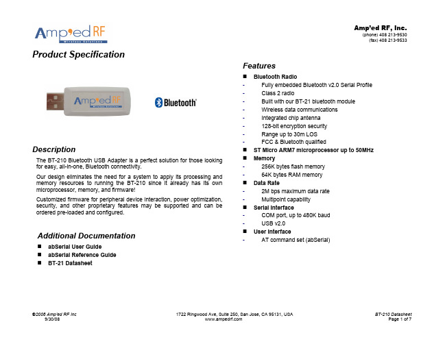
Product Specification
Features
Bluetooth Radio Fully embedded Bluetooth v2.0 Serial Profile Class 2 radio Built with our BT-21 bluetooth module Wireless data communications Integrated chip antenna 128-bit encryption security Range up to 30m LOS FCC & Bluetooth qualified ST Micro ARM7 microprocessor up to 50MHz Memory 256K bytes flash memory 64K bytes RAM memory Data Rate 2M bps maximum data rate Multipoint capability Serial Interface COM port, up to 480K baud USB v2.0 User Interface AT command set (abSerial)
25136中文资料

CHOOSE XTRA•GUARD® 2 FOR:
s s
s s
s
s s
Now Rated To 90°C! Unmatched Resistance to Oils, Fuels, Solvents, and Water Twice the Tensile Strength of PVC Three Times the Tear and Abrasion Resistance of PVC Superior Low-Temperature Flexibility to -20° C Ultraviolet Light Stability (jacket color black) SUPRASHIELD® - Twice as Effective as Foil Shielding
24 AWG (0,23mm2), 7/32 (7x0,20mm), Insulation Thickness: 0.010" (0,25mm) Jacket Thickness Nominal Diameter Part No. No. of Pairs. Inches mm Inches mm
25271 25272 25273 25274 25275 25276 25279 25279/11 25279/15 25279/19 1 2 3 4 5 6 9 11 15 19 0.032 0.032 0.032 0.032 0.032 0.032 0.032 0.032 0.032 0.032 0,81 0,81 0,81 0,81 0,81 0,81 0,81 0,81 0,81 0,81 0.18 0.23 0.25 0.28 0.30 0.31 0.36 0.38 0.43 0.46 4,6 5,8 6,5 7,0 7,5 8,0 9,1 9,7 10,8 11,8
atc中文手册
A T24C256中文资料2009-11-15 09:43特性???? 与1MHz I2C 总线兼容???? 到伏工作电压范围???? 低功耗CMOS 技术???? 写保护功能当WP 为高电平时进入写保护状态???? 64 字节页写缓冲器???? 自定时擦写周期???? 100,000 编程/擦写周期???? 可保存数据100 年???? 8 脚DIP SOIC 封装???? 温度范围商业级工业级和汽车级概述CAT24WC256 是一个256K 位串行CMOS E2PROM 内部含有32768 个字节每字节为8 位CATALYST 公司的先进CMOS 技术实质上减少了器件的功耗CAT24WC256 有一个64 字节页写缓冲器该器件通过I2C 总线接口进行操作管脚描述管脚名称功能A0 A1 地址输入SDA 串行数据/地址SCL 串行时钟WP 写保护Vcc + 电源Vss 地NC 未连接极限参数工作温度工业级-55 +125商业级0 +75贮存温度-65 +150各管脚承受电压 Vcc+Vcc 管脚承受电压 +封装功率损耗Ta=25焊接温度(10 秒) 300口输出短路电流100mA功能描述CAT24WC256 支持I2C 总线数据传送协议I2C 总线协议规定任何将数据传送到总线的器件作为发送器任何从总线接收数据的器件为接收器数据传送是由产生串行时钟和所有起始停止信号的主器件控制的CAT24WC256 是作为从器件被操作的主器件和从器件都可以作为发送器或接收器但由主器件控制传送数据发送或接收的模式管脚描述SCL 串行时钟CAT24WC256 串行时钟输入管脚用于产生器件所有数据发送或接收的时钟这是一个输入管脚SDA 串行数据/地址双向串行数据/地址管脚用于器件所有数据的发送或接收SDA 是一个开漏输出管脚可与其它开漏输出或集电极开路输出进行线或wire-ORWP 写保护当WP 脚连接到Vcc 所有内存变成写保护只能读当WP 引脚连接到Vss 或悬空允许器件进行读/写操作A0 A1 器件地址输入这些管脚为硬连线或者不连接对于单总线系统最多可寻址4 个CAT24WC256 器件参阅器件寻址当这些引脚没有连接时其默认值为0I2C 总线协议I2C 总线协议定义如下1 只有在总线空闲时才允许启动数据传送2 在数据传送过程中当时钟线为高电平时数据线必须保持稳定状态不允许有跳变时钟线为高电平时数据线的任何电平变化将被看作总线的起始或停止信号起始信号时钟线保持高电平期间数据线电平从高到低的跳变作为I2C 总线的起始信号停止信号时钟线保持高电平期间数据线电平从低到高的跳变作为I2C 总线的停止信号器件寻址主器件通过发送一个起始信号启动发送过程然后发送它所要寻址的从器件的地址8 位从器件地址的高5 位固定为10100 见图5 接下来的2 位A1 A0 为器件的地址位最多可以连接4 个器件到同一总线上这些位必须与硬连线输入脚A1 A0 相对应从器件地址的最低位作为读写控制位1表示对从器件进行读操作0 表示对从器件进行写操作在主器件发送起始信号和从器件地址字节后CAT24WC256 监视总线并当其地址与发送的从地址相符时响应一个应答信号通过SDA 线CAT24WC256 再根据读写控制位R/W 的状态进行读或写操作应答信号I2C 总线数据传送时每成功地传送一个字节数据后接收器都必须产生一个应答信号应答的器件在第9 个时钟周期时将SDA 线拉低表示其已收到一个8 位数据CAT24WC256 在接收到起始信号和从器件地址之后响应一个应答信号如果器件已选择了写操作则在每接收一个8 位字节之后响应一个应答信号当CAT24WC256 工作于读模式时在发送一个8 位数据后释放SDA 线并监视一个应答信号一旦接收到应答信号CAT24WC256 继续发送数据如主器件没有发送应答信号器件停止传送数据并等待一个停止信号写操作字节写在字节写模式下主器件发送起始信号和从器件地址信息R/W 位置0 给从器件在从器件送回应答信号后主器件发送两个8 位地址字写入CAT24WC256 的地址指针主器件在收到从器件的应答信号后再发送数据到被寻址的存储单元CAT24WC256 再次应答并在主器件产生停止信号后开始内部数据的擦写在内部擦写过程中CAT24WC256 不再应答主器件的任何请求页写在页写模式下单个写周期内CAT24WC256 最多可以写入64 个字节数据页写操作的启动和字节写一样不同在于传送了一字节数据后主器件允许继续发送63 个字节每发送一个字节后CAT24WC256 将响应一个应答位且内部低6 位地址加1 高位地址保持不变如果主器件在发送停止信号之前发送大于64 个字节地址计数器将自动翻转先前写入的数据被覆盖当所有64 字节接收完毕主器件发送停止信号内部编程周期开始此时所有接收到的数据在单个写周期内写入CAT24WC256应答查询可以利用内部写周期时禁止数据输入这一特性一旦主器件发送停止位指示主器件操作结束时CAT24WC256 启动内部写周期应答查询立即启动包括发送一个起始信号和进行写操作的从器件地址如果CAT24WC256 正在进行内部写操作将不会发送应答信号如果CAT24WC256 已经完成了内部写操作将发送一个应答信号主器件可以继续对CAT24WC256 进行下一次读写操作写保护写保护操作特性可使用户避免由于不当操作而造成对存储区域内部数据的改写当WP 管脚接高时整个寄存器区全部被保护起来而变为只可读取CAT24WC256 可以接收从器件地址和字节地址但是装置在接收到第一个数据字节后不发送应答信号从而避免寄存器区域被编程改写读操作CAT24WC256 读操作的初始化方式和写操作时一样仅把R/W 位置为1 有三种不同的读操作方式立即/当前地址读选择/随机读和连续读立即/当前地址读的地址计数器内容为最后操作字节的地址加1 也就是说如果上次读/写的操作地址为N 则立即读的地址从地址N+1 开始如果N=E 此处E=32767 则计数器将翻转到0 且继续输出数据CAT24WC256接收到从器件地址信号后R/W 位置1 它首先发送一个应答信号然后发送一个8 位字节数据主器件不需发送一个应答信号但要产生一个停止信号选择/随机读选择/随机读操作允许主器件对寄存器的任意字节进行读操作主器件首先通过发送起始信号从器件地址和它想读取的字节数据的地址执行一个伪写操作在CAT24WC256 应答之后主器件重新发送起始信号和从器件地址此时R/W 位置1 CAT24WC256 响应并发送应答信号然后输出所要求的一个8 位字节数据主器件不发送应答信号但产生一个停止信号连续读连续读操作可通过立即读或选择性读操作启动在CAT24WC256 发送完一个8 位字节数据后主器件产生一个应答信号来响应告知CAT24WC256 主器件要求更多的数据对应每个主机产生的应答信号CAT24WC256 将发送一个8 位数据字节当主器件不发送应答信号而发送停止位时结束此操作从CAT24WC256 输出的数据按顺序由N 到N+1 输出读操作时地址计数器在CAT24WC256 整个地址内增加这样整个寄存器区域在可在一个读操作内全部读出当读取的字节超过E 此处E=32767计数器将翻转到零并继续输出数据字节。
AN2526NFH资料
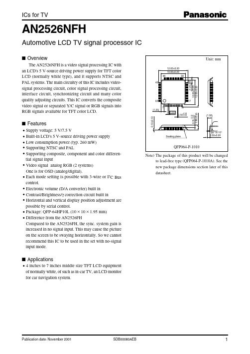
AN2526NFH
Automotive LCD TV signal processor IC
I Overview
The AN2526NFH is a video signal processing IC with an LCD's 5 V-source driving power supply for TFT color LCD (normally white type), and it supports NTSC and PAL systems. The main circuitry of this IC includes videosignal processing circuit, color signal processing circuit, interface circuit, synchronizing circuit and many color quality adjusting circuits. This IC converts the composite video signal or separated Y/C signal or RGB signals into RGB signals available for TFT color LCD.
1 µF 5.1 kΩ NTSC 3.58 MHz PAL 4.43 MHz 0.1 µF
56
VXO
57
58
CLMP (BGP)
R-out
Trap
GND 3
59
GND1 21GBiblioteka mma4.7 µF60
YAP ctl.
VCC1
50 kB
R−Y out
61
20 19
BT152中文资料

BT152中⽂资料GENERAL DESCRIPTIONQUICK REFERENCE DATAGlass passivated thyristors in a plastic SYMBOL PARAMETERMAX.MAX.MAX.UNIT envelope,intended for use in applications requiring high BT152-400R 600R 800R bidirectional blocking voltage V DRM ,Repetitive peak off-state 450650800V capability and high thermal cycling V RRM voltages performance.Typical applications I T(AV)Average on-state current 131313A include motor control,industrial and IT(RMS)RMS on-state current202020A domestic lighting,heating and static I TSMNon-repetitive peak on-state 200200200Aswitching.currentPINNING - TO220ABPIN CONFIGURATIONSYMBOLLIMITING VALUESLimiting values in accordance with the Absolute Maximum System (IEC 134).SYMBOL PARAMETERCONDITIONSMIN.MAX.UNIT -400R -600R -800R V DRM Repetitive peak off-state -45016501800V voltagesI T(AV)Average on-state current half sine wave; T mb ≤ 103 ?C -13A I T(RMS)RMS on-state current all conduction angles-20A I TSMNon-repetitive peak half sine wave; T j = 25 ?C prior to on-state currentsurge t = 10 ms -200A t = 8.3 ms -220A I 2t I 2t for fusingt = 10 ms-200A 2s dI T /dt Repetitive rate of rise of I TM = 50 A; I G = 0.2 A;-200A/µs on-state current after dI G /dt = 0.2 A/µs triggering I GM Peak gate current -5A V GM Peak gate voltage-5V V RGM Peak reverse gate voltage -5V P GM Peak gate power -20W P G(AV)Average gate power over any 20 ms period -0.5W T stg Storage temperature -40150?C T jOperating junction -125Ctemperature1 Although not recommended, off-state voltages up to 800V may be applied without damage, but the thyristor may switch to the on-state. The rate of rise of current should not exceed 15 A/µs.THERMAL RESISTANCESSYMBOL PARAMETERCONDITIONSMIN.TYP.MAX.UNIT R th j-mb Thermal resistance-- 1.1K/W junction to mounting base R th j-aThermal resistance in free air -60-K/Wjunction to ambientSTATIC CHARACTERISTICST j = 25 ?C unless otherwise stated SYMBOL PARAMETER CONDITIONSMIN.TYP.MAX.UNIT I GT Gate trigger current V D = 12 V; I T = 0.1 A -332mA I L Latching current V D = 12 V; I GT = 0.1 A -2580mA I H Holding current V D = 12 V; I GT = 0.1 A -1560mA V T On-state voltage I T = 40 A- 1.4 1.75V V GT Gate trigger voltage V D = 12 V; I T = 0.1 A-0.6 1.5V V D = V DRM(max); I T = 0.1 A; T j = 125 ?C 0.250.4-V I D , I ROff-state leakage currentV D = V DRM(max); V R = V RRM(max); T j = 125 ?C-0.21.0mADYNAMIC CHARACTERISTICST j = 25 ?C unless otherwise stated SYMBOL PARAMETER CONDITIONSMIN.TYP.MAX.UNIT dV D /dt Critical rate of rise of V DM = 67% V DRM(max); T j = 125 ?C;200300-V/µs off-state voltageexponential waveform gate open circuit t gt Gate controlled turn-on V D = V DRM(max); I G = 0.1 A; dI G /dt = 5 A/µs;-2-µs timeI TM = 40 At qCircuit commutated V D = 67% V DRM(max); T j = 125 ?C;-70-µsturn-off timeI TM = 50 A; V R = 25 V; dI TM /dt = 30 A/µs;dV D /dt = 50 V/µs; R GK = 100 ?MECHANICAL DATANotes1. Refer to mounting instructions for TO220 envelopes.2. Epoxy meets UL94 V0 at 1/8".DEFINITIONSData sheet statusObjective specification This data sheet contains target or goal specifications for product development. Preliminary specification This data sheet contains preliminary data; supplementary data may be published later. Product specification This data sheet contains final product specifications.Limiting valuesLimiting values are given in accordance with the Absolute Maximum Rating System (IEC 134). Stress above one or more of the limiting values may cause permanent damage to the device. These are stress ratings only and operation of the device at these or at any other conditions above those given in the Characteristics sections of this specification is not implied. Exposure to limiting values for extended periods may affect device reliability. Application informationWhere application information is given, it is advisory and does not form part of the specification.Philips Electronics N.V. 1997All rights are reserved. Reproduction in whole or in part is prohibited without the prior written consent of the copyright owner.The information presented in this document does not form part of any quotation or contract, it is believed to be accurate and reliable and may be changed without notice. No liability will be accepted by the publisher for any consequence of its use. Publication thereof does not convey nor imply any license under patent or other industrial or intellectual property rights.LIFE SUPPORT APPLICATIONSThese products are not designed for use in life support appliances, devices or systems where malfunction of these products can be reasonably expected to result in personal injury. Philips customers using or selling these products for use in such applications do so at their own risk and agree to fully indemnify Philips for any damages resulting from such improper use or sale.。
AT25F4096中文资料
IC型号:AT25F4096_06 IC描述:的4Mb高速的SPI串行闪存 IC厂商:ATMEL Corporation
AT25F4096_06 中文数据手册(Datasheet) - ATMEL Corporation
第2 页
AT25F4096 启用该 (CS) 通过芯片选择引脚 (SI), ,并通过一个 3线接口的串行数据输入输出 (SO), (SCK). 串行数据和串行时钟 1/8, 组成的全部写周期是完全独立的计时 访问。 块写入顶级顶级 1/4, 1/2 WP 顶部或整个记忆体阵列的保护是启用的状态寄存器编程 。单独写使能和写禁止指令 提供额外的数据保护。硬件数据保护是通过提供 HOLD 针,以防止无意中写状态寄存器的尝试。该 +85°C 脚可暂停而不重置串行 序列任何串行通信。
/ATMEL/AT25F4096_06/3.htm
2011-3-16
ATMEL - AT25F4096_06中文数据手册(第4页)【Soiseek - 搜IC】
Page 1 of 1
IC型号大全
使用Firefox(火狐)浏览器提高10倍以上的搜索速度
ATMEL - AT25F4096_06 AT25F4096_06中文数据手册下载 下载数据手册 (Datasheet) PDF格式 请确保使用最新版Adobe Reader 打开文档 Adobe Reader 9.3 点击下载 数据手册包含IC型号 AT25F4096 AT25F4096Y4-10YH-2.7 AT25F4096W-10SU-2.7 AT25F4096_06
图 524,288 框图
8x2
AT25F4096
2454G–SFLSH–5/06
启用该 通过芯片选择引脚,并通过一个3 线接口的串行数据输入输出 串行数据和串行时钟
东芝芯片资料
0 900Ω 600Ω 19.5K 15K 13K 19K
LA7833引脚功能
引脚
1 2 3 4 4 6 7
功能
接地端 场输出 自举升压电源端 场激励输入 负反馈输入及相位补偿 电源端 场逆程脉冲输出
直流电压
0V 13.6V 25.5V 0.8V 0.8V 26V 1.4V
纹波滤波电路引脚 第二伴音中频输出 调频直流反馈滤波电路引脚
电压
1.8V 0V 1.3V
+2.5V
+5V 2.45V 2.45V
1V 6.4V 0V 0V 2.3V 1.6V 0V +5V 3.6V 4.3V 0V 8V 8.8V 3.5V 5.6V 3.4V 3.5V
RXIK档对地电阻(黑表笔接地)
场AGC 总线时钟端子 总线数据端子
行电源 SECAM识别/载波信号输出
行逆程脉冲输入 复合同步信号输出 行激励信号输出
接地 沙堡脉冲输出 视频信号输出
数字电源
SECAM蓝色差信号输入 SECAM红色差信号输入
亮度信号输入 行AFC滤波
外接视频信号
接地 视频信Leabharlann 输入黑电平检测滤波直流电压(V)
有信号 4.9
800Ω 0
12.5K
12.8K
6K 13K 13K 13K 12.8K 13.2K
0 12.8K 13K 11.5K
1K 12.5K 12K
0 900Ω 600Ω 12.5K 12.2K 11.5K 12K
红笔接地 R×1K档
800Ω 0
19K
27K
5.5K 20K 20K 18K 28K 28K
pt2262_pt2272中文资料

PT2262/PT2272编码解码芯片中文资料PT2262/PT2272是台湾普城公司生产的一种CMOS工艺制造的低功耗低价位通用编解码电路,PT2262/PT2272最多可有12位(A0-A11)三态地址端管脚(悬空,接高电平,接低电平),任意组合可提供531441地址码,PT2262最多可有6位(D0-D5)数据端管脚,设定的地址码和数据码从17脚串行输出,可用于无线遥控发射电路。
编码芯片PT2262发出的编码信号由:地址码、数据码、同步码组成一个完整的码字,解码芯片PT2272接收到信号后,其地址码经过两次比较核对后,VT脚才输出高电平,与此同时相应的数据脚也输出高电平,如果发送端一直按住按键,编码芯片也会连续发射。
当发射机没有按键按下时,PT2262不接通电源,其17脚为低电平,所以315MHz的高频发射电路不工作,当有按键按下时,PT2262得电工作,其第17脚输出经调制的串行数据信号,当17脚为高电平期间315MHz的高频发射电路起振并发射等幅高频信号,当17脚为低平期间3 15MHz的高频发射电路停止振荡,所以高频发射电路完全收控于PT2262的17脚输出的数字信号,从而对高频电路完成幅度键控(ASK调制)相当于调制度为100%的调幅。
PT2262/PT2272特点l CMOS工艺制造,低功耗l 外部元器件少l RC振荡电阻l 工作电压范围宽:2.6-15vl 数据最多可达6位l 地址码最多可达531441种PT2262/PT2272应用范围l 车辆防盗系统l 家庭防盗系统l 遥控玩具l 其他电器遥控PT2262 引脚图:PT2262管脚说明:名称管脚说明A0-A11 1-8、10-13 地址管脚,用于进行地址编码,可置为“0”,“1”,“f”(悬空),D0-D5 7-8、10-13 数据输入端,有一个为“1”即有编码发出,内部下拉Vcc 18 电源正端(+)Vss 9 电源负端(-)TE 14 编码启动端,用于多数据的编码发射,低电平有效;OSC1 16 振荡电阻输入端,与OSC2所接电阻决定振荡频率;OSC2 15 振荡电阻振荡器输出端;Dout 17 编码输出端(正常时为低电平)在具体的应用中,外接振荡电阻可根据需要进行适当的调节,阻值越大振荡频率越慢,编码的宽度越大,发码一帧的时间越长.PT2262参数PT2272 解码电路引脚图:名称管脚说明A0-A11 1-8、10-13 地址管脚,用于进行地址编码,可置为“0”,“1”,“f”(悬空),必须与2262一致,否则不解码D0-D5 7-8、10-13 地址或数据管脚,当做为数据管脚时,只有在地址码与2262一致,数据管脚才能输出与2262数据端对应的高电平,否则输出为低电平,锁存型只有在接收到下一数据才能转换Vcc 18 电源正端(+)Vss 9 电源负端(-)DIN 14 数据信号输入端,来自接收模块输出端OSC1 16 振荡电阻输入端,与OSC2所接电阻决定振荡频率;OSC2 15 振荡电阻振荡器输出端;VT 17解码有效确认输出端(常低)解码有效变成高电平(瞬态)PT2272解码芯片有不同的后缀,表示不同的功能,有L4/M4/L6/M6之分,其中L表示锁存输出,数据只要成功接收就能一直保持对应的电平状态,直到下次遥控数据发生变化时改变。
BTG2500中英文使用说明书
MIC29152BT资料

元器件交易网 MIC29150/29300/29500/29750 Ordering Information
Part Number MIC29150-3.3BT MIC29150-4.2BT MIC29150-5.0BT MIC29150-12BT MIC29150-3.3BU MIC29150-5.0BU MIC29150-12BU MIC29151-3.3BT MIC29151-5.0BT MIC29151-12BT MIC29151-3.3BU MIC29151-5.0BU MIC29151-12BU MIC29152BT MIC29152BU MIC29153BT MIC29153BU MIC29300-3.3BT MIC29300-5.0BT MIC29300-12BT MIC29300-3.3BU MIC29300-5.0BU MIC29300-12BU MIC29301-3.3BT MIC29301-5.0BT MIC29301-12BT MIC29301-3.3BU MIC29301-5.0BU MIC29301-12BU MIC29302BT MIC29302BU MIC29303BT MIC29303BU Temp. Range* Volts Current Package –40 to +125°C –40 to +125°C –40 to +125°C –40 to +125°C –40 to +125°C –40 to +125°C –40 to +125°C –40 to +125°C –40 to +125°C –40 to +125°C –40 to +125°C –40 to +125°C –40 to +125°C –40 to +125°C –40 to +125°C –40 to +125°C –40 to +125°C –40 to +125°C –40 to +125°C –40 to +125°C –40 to +125°C –40 to +125°C –40 to +125°C –40 to +125°C –40 to +125°C –40 to +125°C –40 to +125°C –40 to +125°C –40 to +125°C –40 to +125°C –40 to +125°C –40 to +125°C –40 to +125°C 3.3 4.2 5.0 12 3.3 5.0 12 3.3 5.0 12 3.3 5.0 12 Adj Adj Adj Adj 3.3 5.0 12 3.3 5.0 12 3.3 5.0 12 3.3 5.0 12 Adj Adj Adj Adj 1.5A 1.5A 1.5A 1.5A 1.5A 1.5A 1.5A 1.5A 1.5A 1.5A 1.5A 1.5A 1.5A 1.5A 1.5A 1.5A 1.5A 3.0A 3.0A 3.0A 3.0A 3.0A 3.0A 3.0A 3.0A 3.0A 3.0A 3.0A 3.0A 3.0A 3.0A 3.0A 3.0A TO-220 TO-220 TO-220 TO-220 TO-263 TO-263 TO-263 TO-220-5 TO-220-5 TO-220-5 TO-263-5 TO-263-5 TO-263-5 TO-220-5 TO-263-5 TO-220-5 TO-263-5 TO-220 TO-220 TO-220 TO-263 TO-263 TO-263 TO-220-5 TO-220-5 TO-220-5 TO-263-5 TO-263-5 TO-263-5 TO-220-5 TO-263-5 TO-220-5 TO-263-5 Part Number MIC29500-3.3BT MIC29500-5.0BT MIC29501-3.3BT MIC29501-5.0BT MIC29501-3.3BU MIC29501-5.0BU MIC29502BT MIC29502BU MIC29503BT MIC29503BU MIC29750-3.3BWT MIC29750-5.0BWT MIC29751-3.3BWT MIC29751-5.0BWT MIC29752BWT
BTA225-800B,127;BTA225-600B,127;中文规格书,Datasheet资料
BTA225 series B Three quadrant triacs high commutationNXP Semiconductors Product specificationThree quadrant triacs high commutationBTA225 series BGENERAL DESCRIPTIONQUICK REFERENCE DATAGlass passivated high commutation SYMBOL PARAMETERMAX.MAX.MAX.UNIT triacs in a plastic envelope intended for use in circuits where high static and BTA225-500B 600B 800B dynamic dV/dt and high dI/dt can V DRM Repetitive peak off-state 500600800V occur loads.These devices will voltagescommutate the full rated rms current I T(RMS)RMS on-state current252525A at the maximum rated junction I TSMNon-repetitive peak on-state 190190190Atemperature,without the aid of a currentsnubber.PINNING - TO220ABPIN CONFIGURATIONSYMBOLPIN DESCRIPTION 1main terminal 12main terminal 23gatetabmain terminal 2LIMITING VALUESLimiting values in accordance with the Absolute Maximum System (IEC 134).SYMBOL PARAMETERCONDITIONSMIN.MAX.UNIT-500-600-800V DRM Repetitive peak off-state -60016001800V voltagesI T(RMS)RMS on-state current full sine wave;-25A T mb ≤ 91 ˚C I TSMNon-repetitive peak full sine wave;on-state currentT j = 25 ˚C prior to surge t = 20 ms -190A t = 16.7 ms -209A I 2t I 2t for fusingt = 10 ms-180A 2s dI T /dt Repetitive rate of rise of I TM = 30 A; I G = 0.2 A;100A/µs on-state current after dI G /dt = 0.2 A/µs triggeringI GM Peak gate current -2A V GM Peak gate voltage -5V P GM Peak gate power -5W P G(AV)Average gate power over any 20 ms -0.5W periodT stg Storage temperature -40150˚C T jOperating junction -125˚CtemperatureT1T2G123tab1 Although not recommended, off-state voltages up to 800V may be applied without damage, but the triac may switch to the on-state. The rate of rise of current should not exceed 15 A/µs.high commutationBTA225 series BTHERMAL RESISTANCESSYMBOL PARAMETERCONDITIONSMIN.TYP.MAX.UNIT R th j-mb Thermal resistance full cycle -- 1.0K/W junction to mounting base half cycle -- 1.4K/W R th j-aThermal resistance in free air -60-K/Wjunction to ambientSTATIC CHARACTERISTICST j = 25 ˚C unless otherwise stated SYMBOL PARAMETER CONDITIONS MIN.TYP.MAX.UNIT I GTGate trigger current 2V D = 12 V; I T = 0.1 AT2+ G+21850mA T2+ G-22150mA T2- G-23450mA I LLatching currentV D = 12 V; I GT = 0.1 AT2+ G+-3160mA T2+ G--3490mA T2- G--3060mA I H Holding current V D = 12 V; I GT = 0.1 A -3160mA V T On-state voltage I T = 30 A- 1.3 1.55V V GT Gate trigger voltage V D = 12 V; I T = 0.1 A-0.7 1.5V V D = 400 V; I T = 0.1 A; T j = 125 ˚C 0.250.4-V I DOff-state leakage currentV D = V DRM(max); T j = 125 ˚C-0.10.5mADYNAMIC CHARACTERISTICST j = 25 ˚C unless otherwise stated SYMBOL PARAMETERCONDITIONSMIN.TYP.MAX.UNIT dV D /dt Critical rate of rise of V DM = 67% V DRM(max); T j = 125 ˚C;10004000-V/µs off-state voltageexponential waveform; gate open circuit dI com /dt Critical rate of change of V DM = 400 V; T j = 125 ˚C; I T(RMS) = 25 A;-44-A/ms commutating current without snubber; gate open circuit t gtGate controlled turn-on I TM = 30 A; V D = V DRM(max); I G = 0.1 A;-2-µstimedI G /dt = 5 A/µs2 Device does not trigger in the T2-, G+ quadrant.high commutationBT A225 series BFig.1. Maximum on-state dissipation, P tot , versus rms on-state current, I T(RMS), where α = conduction angle.Fig.2. Maximum permissible non-repetitive peak on-state current I TSM , versus pulse width t p , forsinusoidal currents, t p ≤ 20ms.Fig.3. Maximum permissible non-repetitive peak on-state current I TSM , versus number of cycles, forsinusoidal currents, f = 50 Hz.Fig.4. Maximum permissible rms current I T(RMS) ,versus mounting base temperature T mb .Fig.5. Maximum permissible repetitive rms on-state current I T(RMS), versus surge duration, for sinusoidalcurrents, f = 50 Hz; T mb ≤ 91˚C.Fig.6. Normalised gate trigger voltageV GT (T j )/ V GT (25˚C), versus junction temperature T j .05101520253010203040= 180120906030BTA140IT(RMS) / APtot / WTmb(max) / C1251151059585-5050100150051015202530BTA14091 CTmb / CIT(RMS) / A 10us100us1ms 10ms100ms101001000BTA225T / sITSM / ATI TSM timeI Tj initial = 25 C maxTdI /dt limit T0.010.111001020304050BTA140surge duration / sIT(RMS) / A110100100050100150200BTA140Number of cycles at 50HzITSM / ATI TSM timeI Tj initial = 25 C maxT-50501001500.40.60.811.21.41.6BT136Tj / CVGT(Tj)VGT(25 C)high commutationBT A225 series BFig.7. Normalised gate trigger current I GT (T j )/ I GT (25˚C), versus junction temperature T j .Fig.8. Normalised latching current I L (T j )/ I L (25˚C),versus junction temperature T j .Fig.9. Normalised holding current I H (T j )/ I H (25˚C),versus junction temperature T j .Fig.10. Typical and maximum on-state characteristic.Fig.11. Transient thermal impedance Z th j-mb , versuspulse width t p .Fig.12. Typical, critical rate of change of commutatingcurrent dI com /dt versus junction temperature.-505010015000.511.522.53BTA216Tj / CT2+ G+T2+ G-T2- G-IGT(Tj)IGT(25 C)00.511.522.531020304050607080BTA140VT / VIT / A Tj = 125 C Tj = 25 CVo = 1.073 V Rs = 0.015 ohmstyp max-505010015000.511.522.53TRIACTj / CIL(Tj)IL(25 C)0.0010.010.1110BTA140tp / sZth j-mb (K/W)10us0.1ms 1ms10ms 0.1s 1s 10st pP tDbidirectionalunidirectional-505010015000.511.522.53TRIACTj / CIH(Tj)IH(25C)204060801001201401101001000BTA225Tj / CdIcom/dt (A/ms)high commutationBTA225 series BMECHANICAL DATADimensions in mm Net Mass: 2 gFig.13. TO220AB; pin 2 connected to mounting base.Notes1. Refer to mounting instructions for TO220 envelopes.2. Epoxy meets UL94 V0 at 1/8".10,3max 3,72,83,03,0 max not tinned1,3max (2x)1232,40,64,5max5,9min15,8max1,32,54 2,540,9 max (3x)13,5minLegal informationDATA SHEET STATUSNotes1.Please consult the most recently issued document before initiating or completing a design.2.The product status of device(s) described in this document may have changed since this document was publishedand may differ in case of multiple devices. The latest product status information is available on the Internet at URL . DOCUMENT STATUS (1)PRODUCT STATUS (2)DEFINITIONObjective data sheet Development This document contains data from the objective specification for product development.Preliminary data sheet Qualification This document contains data from the preliminary specification. Product data sheet ProductionThis document contains the product specification.DEFINITIONSProduct specification ⎯ The information and data provided in a Product data sheet shall define the specification of the product as agreed between NXP Semiconductors and its customer, unless NXPSemiconductors and customer have explicitly agreed otherwise in writing. In no event however, shall an agreement be valid in which the NXP Semiconductors product is deemed to offer functions and qualities beyond those described in the Product data sheet.DISCLAIMERSLimited warranty and liability ⎯ Information in this document is believed to be accurate and reliable. However, NXP Semiconductors does not give anyrepresentations or warranties, expressed or implied, as to the accuracy or completeness of such information and shall have no liability for the consequences of use of such information.In no event shall NXP Semiconductors be liable for any indirect, incidental, punitive, special or consequential damages (including - without limitation - lost profits, lost savings, business interruption, costs related to the removal or replacement of any products or reworkcharges) whether or not such damages are based on tort (including negligence), warranty, breach of contract or any other legal theory.Notwithstanding any damages that customer might incur for any reason whatsoever, NXP Semiconductors’aggregate and cumulative liability towards customer for the products described herein shall be limited inaccordance with the Terms and conditions of commercial sale of NXP Semiconductors.Right to make changes ⎯ NXP Semiconductors reserves the right to make changes to informationpublished in this document, including without limitation specifications and product descriptions, at any time and without notice. This document supersedes and replaces all information supplied prior to the publication hereof.Suitability for use ⎯ NXP Semiconductors products are not designed, authorized or warranted to be suitable for use in life support, life-critical or safety-critical systems or equipment, nor in applications where failure or malfunction of an NXP Semiconductors product can reasonably be expected to result in personal injury, death or severeproperty or environmental damage. NXP Semiconductors accepts no liability for inclusion and/or use of NXP Semiconductors products in such equipment orapplications and therefore such inclusion and/or use is at the customer’s own risk.Applications ⎯ Applications that are described herein for any of these products are for illustrative purposes only. NXP Semiconductors makes no representation or warranty that such applications will be suitable for the specified use without further testing or modification. Customers are responsible for the design and operation of their applications and products using NXPSemiconductors products, and NXP Semiconductors accepts no liability for any assistance with applications or customer product design. It is customer’s sole responsibility to determine whether the NXPSemiconductors product is suitable and fit for thecustomer’s applications and products planned, as well as for the planned application and use of customer’s third party customer(s). Customers should provide appropriate design and operating safeguards to minimize the risks associated with their applications and products.Legal informationNXP Semiconductors does not accept any liability related to any default, damage, costs or problem which is based on any weakness or default in the customer’s applications or products, or the application or use by customer’s third party customer(s). Customer is responsible for doing all necessary testing for the customer’s applications and products using NXP Semiconductors products in order to avoid a default of the applications and the products or of the application or use by customer’s third partycustomer(s). NXP does not accept any liability in this respect.Limiting values ⎯ Stress above one or more limiting values (as defined in the Absolute Maximum Ratings System of IEC 60134) will cause permanent damage to the device. Limiting values are stress ratings only and (proper) operation of the device at these or any other conditions above those given in the Recommended operating conditions section (if present) or theCharacteristics sections of this document is not warranted. Constant or repeated exposure to limiting values will permanently and irreversibly affect the quality and reliability of the device.Terms and conditions of commercial sale ⎯ NXP Semiconductors products are sold subject to the general terms and conditions of commercial sale, as published at /profile/terms, unless otherwiseagreed in a valid written individual agreement. In case an individual agreement is concluded only the terms and conditions of the respective agreement shall apply. NXP Semiconductors hereby expressly objects to applying the customer’s general terms and conditions with regard to the purchase of NXP Semiconductors products by customer.No offer to sell or license ⎯ Nothing in this document may be interpreted or construed as an offer to sell products that is open for acceptance or the grant, conveyance or implication of any license under any copyrights, patents or other industrial or intellectual property rights.Export control ⎯ This document as well as the item(s) described herein may be subject to export controlregulations. Export might require a prior authorization from national authorities.Quick reference data ⎯ The Quick reference data is an extract of the product data given in the Limiting values and Characteristics sections of this document, and as such is not complete, exhaustive or legally binding.Non-automotive qualified products ⎯ Unless this data sheet expressly states that this specific NXPSemiconductors product is automotive qualified, the product is not suitable for automotive use. It is neither qualified nor tested in accordance with automotive testing or application requirements. NXP Semiconductors accepts no liability for inclusion and/or use of non-automotive qualified products in automotive equipment or applications.In the event that customer uses the product for design-in and use in automotive applications to automotivespecifications and standards, customer (a) shall use the product without NXP Semiconductors’ warranty of the product for such automotive applications, use and specifications, and (b) whenever customer uses the product for automotive applications beyond NXPSemiconductors’ specifications such use shall be solely at customer’s own risk, and (c) customer fully indemnifies NXP Semiconductors for any liability, damages or failed product claims resulting from customer design and use of the product for automotive applications beyond NXP Semiconductors’ standard warranty and NXP Semiconductors’ product specifications.Contact informationFor additional information please visit: For sales offices addresses send e-mail to: salesaddresses@Customer notificationThis data sheet was changed to reflect the new company name NXP Semiconductors, including new legal definitions and disclaimers. No changes were made to the content, except for the legal definitions and disclaimers. © NXP B.V. 2011All rights are reserved. Reproduction in whole or in part is prohibited without the prior written consent of the copyright owner.The information presented in this document does not form part of any quotation or contract, is believed to be accurate and reliable and may be changed without notice. No liability will be accepted by the publisher for any consequence of its use. Publication thereof does not convey nor imply any license under patent- or other industrial or intellectual property rights.Printed in The Netherlands分销商库存信息:NXPBTA225-800B,127BTA225-600B,127。
BY252中文资料

DC COMPONENTS CO., LTD.
R
115
NEXT EXIT BACK NEXT EXI BACK EXIT NEXT BACK
SYMBOL Maximum Recurrent Peak Reverse Voltage Maximum RMS Voltage Maximum DC Blocking Voltage Maximum Average Forward Rectified Current .375*(9.5mm) lead length at T L = 105oC Peak Forward Surge Current 8.3 ms single half sine-wave superimposed on rated load (JEDEC Method) Maximum Instantaneous Forward Voltage at 3.0A DC Maximum DC Reverse Current @T A = 25 oC at Rated DC Blocking Voltage @T A = 100 o C Maximum Full Load Reverse Current Average, Full Cycle .375*(9.5mm) lead length at T L = 75oC Typical Junction Capacitance (Note) Typical Thermal Resistance Operating and Storage Temperature Range NOTES : Measured at 1 MHZ and applied reverse voltage of 4.0 volts VRRM VRMS VDC IO I FSM VF
PCA82C250中文资料
广州周立功单片机发展有限公司 Tel: (020)38730976 38730977 Fax:38730925
7 结论 ...................................................................................................................... 15 8 参考文献 ............................................................................................................... 15 附录 1 缩写和定义 ................................................................................................... 16 附录 2 节点输入电压的计算..................................................................................... 17 附录 3 最大总线线路长度的计算 ............................................................................. 18
PCx82C200 SJA1000 等 而媒体相关接口负责连接传输媒体 譬如将总线节点连接到总线的连接器 像
Philips 的 TJA1050[3]或 PCA82C250[4]等收发器
SPECIFICATION
OSI-LAYER
IMPLEMENTATION
TO BE SPECIFIED BY THE SYSTEM DESIGNER
MIC2592B-2YTQ;MIC2592B-2YTQ TR;MIC2592B-2BTQ;MIC2592B-2BTQ TR;中文规格书,Datasheet资料
depending upon the CGS of the external MOSFETs. These components are not required for MIC2592B operation but can be implemented for GATE output slew rate control (application specific)
48 47 46 45 44 43 42 41 40 39 38 37 /FAULTA CFILTERA 12VGATEA GPI_A0 12VINA /PWRGDA NC 12VSENSEA /FORCE_ONA 12VOUTA VSTBYA 3VINA 1 2 3 4 5 6 7 8 9 10 11 12 13 14 15 16 17 18 19 20 21 22 23 24
/PWRGDA /PWRGDB /FAULTA /FAULTB
3VINB 3VSENSEB 3VGATEB
25 24
23 21 22 17 33 46 #
*R3VGATEB 15
Si4420DY 3.3V 3.0A
41
SMBus Base Address VSTBY
A0 A1 A2 /INT SCL SDA
VSTBYA VSTBYB
20
VAUXA 12VINA
15
0.1F
110k 1%
2
RFILTER[A&B]
5
12VSENSEA CFILTERA CFILTERB 12VGATEA 12VOUTA
8 # CGS 22nF
VSTBY
C1 C2 100k
35
3 #
*R12VGATEA 15
at25sf041手册
at25sf041手册AT25SF041是一种可编程闪存芯片,因其容量大、速度快,被广泛应用于各种电子设备中。
本手册将详细介绍AT25SF041的功能、参数以及使用方法,帮助用户更好地了解和使用该芯片。
一、芯片概述AT25SF041是一种具有4M位(512K字节)容量的串行闪存芯片。
它采用SPI(串行外设接口)通信协议,读取和写入速度较快,能够满足多种应用的需求。
二、芯片参数1.容量:AT25SF041的总容量为4M位,相当于512K字节。
用户可以根据自己的需要,将数据存储在芯片的相应地址中。
2.供电电压:芯片的工作电压范围为2.7V至3.6V,可以适应不同供电环境的要求。
3.擦除和编程速度:芯片支持高速擦除和编程操作。
擦除操作需要约2ms的时间,编程操作需要约1.5ms的时间。
4.工作温度范围:芯片能够在-40℃至85℃的温度范围内正常工作,适用于不同环境条件下的使用。
5.封装形式:AT25SF041的标准封装形式为8引脚的SOIC(小外形集成电路)封装,便于与其他电子元件进行连接。
三、芯片应用AT25SF041广泛应用于各种电子设备中,主要用于数据存储和代码存储。
以下是其常见的应用场景:1.汽车电子:AT25SF041可以作为汽车电子设备中的数据存储器,用于存储行车记录、车辆配置信息等。
2.通信设备:芯片可以用来存储通信设备中的固件代码,提供可靠的存储和读取功能。
3.工业控制:AT25SF041可用于工业控制系统中的程序代码存储,确保系统的正常运行。
4.家用电器:芯片可以应用于家用电器中,用于存储各种控制参数和用户设置。
四、芯片使用方法1.芯片接口:AT25SF041采用SPI通信协议,具有SI(串行输入)、SO(串行输出)、CLK(时钟)和CS(片选)等4个接口引脚。
2.数据读取:通过配置SI、SO、CLK和CS等接口,用户可以向芯片发送读取命令,并通过SO接口获取数据。
3.数据写入:用户可以将待写入的数据发送到SI接口,并通过配置CLK和CS等接口,向芯片发送写入命令。
bt136中文资料

bt136中文资料篇一:双向可控硅产品命名双向可控硅为什么称为“TRIAC”三端:TRIode(取前三个字母)交流半导体开关:ACemiconductorwitch(取前两个字母)以上两组名词组合成“TRIAC”中文译意“三端双向可控硅开关”。
由此可见“TRIAC”是双向可控硅的统称。
双向:Bi-directional(取第一个字母)控制:Controlled(取第一个字母)整流器:Rectifier(取第一个字母)再由这三组英文名词的首个字母组合而成:“BCR”中文译意:双向可控硅。
以“BCR”来命名双向可控硅的典型厂家如日本三菱,如:BCR1AM-12、BCR8KM、BCR08AM等等。
双向:Bi-directional(取第一个字母)三端:Triode(取第一个字母)由以上两组单词组合成“BT”,也是对双向可控硅产品的型号命名,典型的生产商如:意法ST公司、荷兰飞利浦-Philip公司,均以此来命名双向可控硅。
Philip公司的产品型号前缀为“BTA”字头的,通常是指三象限的双向可控硅。
而意法ST公司,则以“BT”字母为前缀来命名元件的型号并且在“BT”后加“A”或“B”来表示绝缘与非绝缘组合成:“BTA”、“BTB”系列的双向可控硅型号,如:三象限/绝缘型/双向可控硅:BTA06-600C、BTA12-600B、BTA16-600B、BTA41-600B等等;四象限/非绝缘/双向可控硅:BTB06-600C、BTB12-600B、BTB16-600B、BTB41-600B等等;ST公司所有产品型号的后缀字母(型号最后一个字母)带“W”的,均为“三象限双向可控硅”。
如“BW”、“CW”、“SW”、“TW”;代表型号如:BTB12-600BW、BTA26-700CW、BTA08-600SW、、、、等等。
至于型号后缀字母的触发电流,各个厂家的代表含义如下:PHILIPS公司:D=5mA,E=10mA,C=15mA,F=25mA,G=50mA,R=200uA或5mA,型号没有后缀字母之触发电流,通常为25-35mA;PHILIPS公司的触发电流代表字母没有统一的定义,以产品的封装不同而不同。
2SJ352中文资料

2SJ352中⽂资料2SJ351, 2SJ352Silicon P-Channel MOS FETADE-208-1431st. EditionApplicationLow frequency power amplifierComplementary pair with 2SK2220, 2SK2221FeaturesHigh power gainExcellent frequency responseHigh speed switchingWide area of safe operationEnhancement-modeGood complementary characteristicsEquipped with gate protection diodesOrdering InformationType No.VDSX2SJ351–180 V2SJ352–200 V2SJ351, 2SJ3522OutlineAbsolute Maximum Ratings (Ta = 25°C)ItemSymbol Ratings Unit Drain to source voltage 2SJ351V DSX–180V2SJ352–200Gate to source voltage V GSS ±20V Drain currentI D –8A Body to drain diode reverse drain current I DR –8A Channel dissipation Pch*1100W Channel temperature Tch 150°C Storage temperature Tstg –55 to +150°C Note:1.Value at T C = 25°C2SJ351, 2SJ3523Electrical Characteristics (Ta = 25°C)ItemSymbol Min Typ Max Unit Test conditions Drain to source 2SJ351V (BR)DSX–180——VI D = –10 mA, V GS = 10 Vbreakdown voltage2SJ352–200——Gate to source breakdown voltageV (BR)GSS ±20——V I G = ±100 µA, V DS = 0Gate to source cutoff voltage V GS(off)–0.15—–1.45V I D = –100 mA, V DS =–10 V Drain to source saturation voltageV DS(sat)——–12V I D = –8 A, V GD = 0*1Forward transfer admittance |y fs |0.7 1.0 1.4S I D = –3 A, V DS = –10 V*1Input capacitance Ciss —800—pF V GS = 5 V, V DS = –10 V,Output capacitanceCoss —1000—pF f = 1 MHzReverse transfer capacitance Crss —18—pF Turn-on time t on —320—ns V DD = –30 V, I D = –4 A Turn-off time t off—120—nsNote:1.Pulse test2SJ351, 2SJ35242SJ351, 2SJ3526Hitachi CodeJEDECEIAJWeight (reference value)TO-3P—Conforms5.0 gUnit: mmCautions1.Hitachi neither warrants nor grants licenses of any rights of Hitachi’s or any third party’s patent,copyright, trademark, or other intellectual property rights for information contained in this document.Hitachi bears no responsibility for problems that may arise with third party’s rights, includingintellectual property rights, in connection with use of the information contained in this document.2.Products and product specifications may be subject to change without notice. Confirm that you have received the latest product standards or specifications before final design, purchase or use.3.Hitachi makes every attempt to ensure that its products are of high quality and reliability. However,contact Hitachi’s sales office before using the product in an application that demands especially high quality and reliability or where its failure or malfunction may directly threaten human life or cause risk of bodily injury, such as aerospace, aeronautics, nuclear power, combustion control, transportation,traffic, safety equipment or medical equipment for life support.4.Design your application so that the product is used within the ranges guaranteed by Hitachi particularly for maximum rating, operating supply voltage range, heat radiation characteristics, installationconditions and other characteristics. Hitachi bears no responsibility for failure or damage when used beyond the guaranteed ranges. Even within the guaranteed ranges, consider normally foreseeable failure rates or failure modes in semiconductor devices and employ systemic measures such as fail-safes, so that the equipment incorporating Hitachi product does not cause bodily injury, fire or other consequential damage due to operation of the Hitachi product.5.This product is not designed to be radiation resistant.6.No one is permitted to reproduce or duplicate, in any form, the whole or part of this document without written approval from Hitachi.7.Contact Hitachi’s sales office for any questions regarding this document or Hitachi semiconductor products.Hitachi, Ltd.Semiconductor & Integrated Circuits.Nippon Bldg., 2-6-2, Ohte-machi, Chiyoda-ku, Tokyo 100-0004, Japan Tel: Tokyo (03) 3270-2111 Fax: (03) 3270-5109 Copyright ' Hitachi, Ltd., 1999. All rights reserved. Printed in Japan.Hitachi Asia Pte. Ltd.16 Collyer Quay #20-00Hitachi TowerSingapore 049318Tel: 535-2100Fax: 535-1533URLNorthAmerica : http:/doc/bfe7be20915f804d2b16c12b.html /Europe :/doc/bfe7be20915f804d2b16c12b.html /hel/ecg Asia (Singapore):/doc/bfe7be20915f804d2b16c12b.html .sg/grp3/sicd/index.htm Asia (Taiwan):/doc/bfe7be20915f804d2b16c12b.html /E/Product/SICD_Frame.htm Asia (HongKong):/doc/bfe7be20915f804d2b16c12b.html /eng/bo/grp3/index.htm Japan :http://www.hitachi.co.jp/Sicd/indx.htmHitachi Asia Ltd.Taipei Branch Office3F, Hung Kuo Building. No.167, Tun-Hwa North Road, Taipei (105)Tel: <886> (2) 2718-3666Fax: <886> (2) 2718-8180 Hitachi Asia (Hong Kong) Ltd.Group III (Electronic Components)7/F., North Tower, World Finance Centre,Harbour City, Canton Road, Tsim Sha Tsui,Kowloon, Hong Kong Tel: <852> (2) 735 9218Fax: <852> (2) 730 0281 Telex: 40815 HITEC HXHitachi Europe Ltd.Electronic Components Group.Whitebrook ParkLower Cookham Road MaidenheadBerkshire SL6 8YA, United Kingdom Tel: <44> (1628) 585000Fax: <44> (1628) 778322Hitachi Europe GmbHElectronic components Group Dornacher Stra§e 3D-85622 Feldkirchen, Munich GermanyTel: <49> (89) 9 9180-0Fax: <49> (89) 9 29 30 00Hitachi Semiconductor (America) Inc.179 East Tasman Drive,San Jose,CA 95134 Tel: <1> (408) 433-1990Fax: <1>(408) 433-0223For further information write to:。
BTB25-800B中文资料

1/9®BTA/BTB24,BTA25,BTA26and T25SeriesSNUBBERLESS ™&STANDARD25A TRIAC SSeptember 2000-Ed:3MAIN FEATURES:DESCRIPTIONAvailable either in through-hole of surface and T25mount packages,the BTA/BTB24-25-26triac series is suitable for general purpose AC power switching.They can be used as an ON/OFF function in applications such as static relays,heating regulation,water heaters,induction motor starting circuits...or for phase control operation in high power motor speed controllers,soft start circuits...The snubberless versions (BTA/BTB...W and T25series)are specially recommended for use on inductive loads,thanks to their high commutation performances.By using an internal ceramic pad,the BTA series provides voltage insulated tab (rated at 2500V RMS)complying with UL standards (File ref.:E81734).Symbol Value Unit I T(RMS)25A V DRM /V RRM 600and 800V I GT (Q 1)35to 50mAABSOLUTE MAXIMUM RATINGSSymbol ParameterValueUnit I T(RMS)RMS on-state current (full sine wave)D P AK TO-220AB Tc =100°C 25ARD91TOP3Ins.Tc =90°C TO-220AB Ins.Tc =75°C I TSM Non repetitive surge peak on-state current (full cycle,Tj initial =25°C)F =60Hz t =16.7ms 260A F =50Hzt =20ms250I t I t Value for fusingtp =10ms450A s dI/dtCritical rate of rise of on-state current I G =2x I GT ,tr ≤100nsF =120Hz Tj =125°C 50A/µs V DSM /V RSM Non repetitive surge peak off-statevoltagetp =10ms Tj =25°C V DRM /V RRM+100V I GM Peak gate currenttp =20µsTj =125°C 4A P G(AV)Average gate power dissipation Tj =125°C1W T stg T jStorage junction temperature range Operating junction temperature range-40to +150-40to +125°C GA2A1GA2A2A1GA2A2A1TO-220AB (BTB24)TO-220AB Insulated (BTA24)TOP3Insulated (BTA26)A1A2GA2A2GA1A2A1GD 2PAK (T25G)RD91(BTA25)BTA/BTB24,BTA25,BTA26and T25Series2/9ELECTRICAL CHARACTERISTICS (Tj =25°C,unless otherwise specified)sSNUBBERLESS ™(3Quadrants)T25-G,BTA/BTB24...W,BTA25...W,BTA26...WsSTANDARD (4Quadrants):BTA25...B,BTA26...BSTATIC CHARACTERISTICSNote 1:minimum IGT is guaranted at 5%of IGT max.Note 2:for both polarities of A2referenced to A1Symbol Test ConditionsQuadrantT25BTA/BTB UnitT2535CW BW I GT (1)V D =12V R L =33ΩI -II -III MAX.353550mA V GT I -II -III MAX. 1.3V V GD V D =V DRM R L =3.3k ΩTj =125°CI -II -IIIMIN.0.2V I H (2)I T =500mA MAX.505075mA I L I G =1.2I GTI -III MAX.707080mA II8080100dV/dt (2)V D =67%V DRM gate open Tj =125°CMIN.5005001000V/µs (dI/dt)c (2)Without snubberTj =125°CMIN.131322A/msSymbol Test ConditionsQuadrant Value Unit I GT (1)V D =12VR L =33ΩI -II -III IV MAX.50100mA V GT ALL MAX. 1.3V V GD V D =V DRM R L =3.3k ΩTj =125°CALLMIN.0.2V I H (2)I T =500mA MAX.80mA I L I G =1.2I GTI -III -IVMAX.70mAII160dV/dt (2)V D =67%V DRM gate open Tj =125°CMIN.500V/µs (dV/dt)c (2)(dI/dt)c =13.3A/msTj =125°CMIN.10V/µs Symbol Test ConditionsValue Unit V TM (2)I TM =35Atp =380µsTj =25°C MAX. 1.55V V to (2)Threshold voltage Tj =125°C MAX.0.85V R d (2)Dynamic resistance Tj =125°C MAX.16m ΩI DRM I RRMV DRM =V RRMTj =25°C MAX.5µA Tj =125°C3mABTA/BTB24,BTA25,BTA26and T25Series3/9THERMAL RESISTANCESS:Copper surface under tabPRODUCT SELECTORBTB:Non insulated TO-220AB packageORDERING INFORMATIONSymbol ParameterValue Unit R th(j-c)Junction to case (AC)D PAK TO-220AB 0.8°C/WRD91(Insulated)TOP3Insulated 1.1TO-220AB Insulated1.7R th(j-a)Junction to ambientS =1cmD PAK 45°C/WTOP3Insulated 50TO-220AB 60TO-220AB InsulatedPart NumberVoltage (xxx)SensitivityType Package 600V800V BTB24-xxxB X X 50mA Standard TO-220AB BTA/BTB24-xxxBW X X 50mA Snubberless TO-220AB BTA/BTB24-xxxCW X X 35mA Snubberless TO-220AB BTA25-xxxB X X 50mA Standard RD-91BTA25-xxxBW X X 50mA Snubberless RD-91BTA25-xxxCW X X 35mA Snubberless RD-91BTA26-xxxB X X 50mA Standard TOP3Ins.BTA26-xxxBW X X 50mA Snubberless TOP3Ins.BTA26-xxxCW X X 35mA Snubberless TOP3Ins.T2535-xxxGXX35mASnubberlessDPAK BT A 24-600BWTRIAC SERIES INSULATION:A:insulatedB:non insulatedCURRENT:24:25A in TO-220AB 25:25A in Rd9126:25A in TOP3SENSITIVITY &TYPE B:50mA STANDARDBW:50mA SNUBBERLESS CW:35mA SNUBBERLESSVOLTAGE:600:600V 800:800VBTA/BTB24,BTA25,BTA26and T25Series4/9OTHER INFORMATIONNote :xxx=voltage,y =sensitivity,z =typePart NumberMarkingWeight Base quantity Packing mode BTA/BTB24-xxxyz BTA/BTB24xxxyz 2.3g 250Bulk BTA25-xxxyz BTA25xxxyz 20g 25Bulk BTA26-xxxyz BTA26xxxyz 4.5g 120Bulk T2535-xxxG T2535xxxG 1.5g 50Tube T2535-xxxG-TRT2535xxxG1.5g1000Tape &reelT 2535-600G(-TR)TRIAC SERIES SENSITIVITY:35:35mAVOLTAGE:600:600V 800:800VCURRENT:25APACKAGE:G:D PAK2PACKING MODE:Blank:Tube-TR:Tape &ReelBTA/BTB24,BTA25,BTA26and T25Series5/9Fig.1:Maximum power dissipation versus RMS on-state current (full cycle).Fig.2-1:RMS on-state current versus case temperature (full cycle).Fig.2-2:D P AK RMS on-state current versus ambient temperature (printed circuit board FR4,copper thickness:35µm),full cycle.Fig.3:Relative variation of thermal impedance versus pulse duration.Fig.4:On-state characteristics (maximumvalues).Fig.5:Surge peak on-state current versus number of cycles.5101520250510********IT(RMS)(A)P (W)025507510012551015202530Tc(°C)IT(RMS)(A)BTA24BTB/T25BTA25/262550751001250.00.51.01.52.02.53.03.54.0Tamb(°C)IT(RMS)(A)D PAK (S=1cm )221E-31E-21E-11E+01E+11E+25E+21E-31E-21E-11E+0tp (s)K=[Zth/Rth]Zth(j-c)Zth(j-a)BTA/BTB24/T25Zth(j-a)BTA260.51.01.52.02.53.03.54.0 4.5110100300VTM (V)ITM (A)Tj=25°CTj maxTj max.Vto =0.85V Rd =16m Ω110100100050100150200250300Number of cyclesITSM (A)Non repetitive Tj initial=25°CRepetitive Tc=75°COne cyclet=20msBTA/BTB24,BTA25,BTA26and T25Series6/9Fig.6:Non-repetitive surge peak on-state current for a sinusoidal pulse with width tp <10ms,and corresponding value of I t.Fig.7:Relative variation of gate trigger current,holding current and latching current versus junction temperature (typical values).Fig.8:Relative variation of critical rate of decrease of main current versus (dV/dt)c (typical values).Fig.9:Relative variation of critical rate of decrease of main current versus junction temperature.Fig.10:D PAK Thermal resistance junction to ambient versus copper surface under tab (printed circuit board FR4,copper thickness:35µm).0.010.101.0010.0010010003000tp (ms)ITSM (A),I t (A s)Tj initial=25°CITSMI tdI/dt limitation:50A/µs-40-20204060801001201400.00.51.01.52.02.5Tj(°C)IGT,IH,IL[Tj]/IGT,IH,IL[Tj=25°C]IGTIH &IL0.11.010.0100.00.40.60.81.01.21.41.61.82.02.22.4(dV/dt)c (V/µs)(dI/dt)c [(dV/dt)c]/Specified (dI/dt)cBW/CW/T2535B2550751001250123456Tj (°C)(dI/dt)c [Tj]/(dI/dt)c [Tj specified]4812162024283236401020304050607080S(cm )Rth(j-a)(°C/W)D PAKBTA/BTB24,BTA25,BTA26and T25Series7/9PACKAGE MECHANICAL DATA D PAK (Plastic)REF.DIMENSIONSMillimeters Inches Min.Typ.Max.Min.Typ.Max.A 4.30 4.600.1690.181A1 2.49 2.690.0980.106A20.030.230.0010.009B 0.700.930.0270.037B2 1.25 1.400.0480.055C 0.450.600.0170.024C2 1.21 1.360.0470.054D 8.959.350.3520.368E 10.0010.280.3930.405G 4.88 5.280.1920.208L 15.0015.850.5900.624L2 1.27 1.400.0500.055L3 1.40 1.750.0550.069R 0.400.016V20°8°0°8°AC2DR2.0MIN.FLAT ZONEA2V2CA1GLL3L2BB2EFOOTPRINT DIMENSIONS (in millimeters)D PAK (Plastic)8.903.701.305.0816.9010.30BTA/BTB24,BTA25,BTA26and T25Series8/9PACKAGE MECHANICAL DATA RD91(Plastic)REF.DIMENSIONSMillimeters InchesMin.Max.Min.Max.A 40.00 1.575A129.9030.30 1.1771.193A222.000.867B 27.00 1.063B113.5016.500.5310.650B224.000.945C 14.000.551C1 3.500.138C2 1.95 3.000.0770.118E30.700.900.0270.035F 4.00 4.500.1570.177I 11.2013.600.4410.535L1 3.10 3.500.1220.138L2 1.70 1.900.0670.075N133°43°33°43°N228°38°28°38°A2L2L1B2CC2A1C1B1N1BFIAE3N2PACKAGE MECHANICAL DATA TOP3(Plastic)REF.DIMENSIONSMillimeters Inches Min.Typ.Max.Min.Typ.Max.A 4.4 4.60.1730.181B 1.45 1.550.0570.061C 14.3515.600.5650.614D 0.50.70.0200.028E 2.7 2.90.1060.114F 15.816.50.6220.650G 20.421.10.8150.831H 15.115.50.5940.610J 5.4 5.650.2130.222K 3.4 3.650.1340.144L 4.08 4.170.1610.164P 1.201.400.0470.055R4.600.181BTA/BTB24,BTA25,BTA26and T25Series9/9PACKAGE MECHANICAL DATA TO-220AB (Plastic)REF.DIMENSIONSMillimeters Inches Min.Typ.Max.Min.Typ.Max.A 15.2015.900.5980.625a1 3.750.147a213.0014.000.5110.551B 10.0010.400.3930.409b10.610.880.0240.034b2 1.23 1.320.0480.051C 4.40 4.600.1730.181c10.490.700.0190.027c2 2.40 2.720.0940.107e 2.40 2.700.0940.106F 6.20 6.600.2440.259I 3.75 3.850.1470.151I415.8016.4016.800.6220.6460.661L 2.65 2.950.1040.116l2 1.14 1.700.0440.066l3 1.14 1.700.0440.066M2.600.102MBl4Cb2a2l2c2l3b1a1AFLIec1Information furnished is believed to be accurate and reliable.However,STMicroelectronics assumes no responsibility for the consequences of use of such information nor for any infringement of patents or other rights of third parties which may result from its use.No license is granted by implication or otherwise under any patent or patent rights of STMicroelectronics.Specifications mentioned in this publication are subject to change without notice.This publication supersedes and replaces all information previously supplied.STMicroelectronics products are not authorized for use as critical components in life support devices or systems without express written approval of STMicroelectronics.©The ST logo is a registered trademark of STMicroelectronics ©2000STMicroelectronics -Printed in Italy -All Rights ReservedSTMicroelectronics GROUP OF COMPANIESAustralia -Brazil -China -Finland -France -Germany -Hong Kong -India -Italy -Japan -Malaysia -Malta -MoroccoSingapore -Spain -Sweden -Switzerland -United Kingdom。
- 1、下载文档前请自行甄别文档内容的完整性,平台不提供额外的编辑、内容补充、找答案等附加服务。
- 2、"仅部分预览"的文档,不可在线预览部分如存在完整性等问题,可反馈申请退款(可完整预览的文档不适用该条件!)。
- 3、如文档侵犯您的权益,请联系客服反馈,我们会尽快为您处理(人工客服工作时间:9:00-18:30)。
元器件交易网
元器件交易网
元器件交易网
元器件交易网
元器件交易网
元器件交易网
元器件交易网
元器件交易网
元器件交易网
元器件交易网
元器件交易网
元器件交易网
元器件交易网
元器件交易网
元器件交易网
元器件交易网
元器件交易网
元器件交易网
元器件交易网
元器件交易网
元器件交易网
元器件交易网
元器件交易网
元器件交易网
元器件交易网
元器件交易网
元器件交易网
元器件交易网
元器件交易网
元器件交易网
元器件交易网