PT6554L中文资料
华润矽微代理海立辉PT4205 PT4115 PT1102 PT4207

华润矽威科技(上海)有限公司
PT4205_DSB Rev CH_0.1
Page 4
PT4205
30V/1.2A 高调光比 LED 恒流驱动器
封装信息
SOT89-5 封装
D D1 A
E1
b1
L
e e1
b
E
c
SYMBOL A b b1 c D D1 E E1 e e1 L
MHz mV % µA µA V V V V kHz uA
VCSN VCSN_hys ICSN
关断电流
平均采样电压 采样电压迟滞 CSN管脚输入电流
IOFF DIM输入 VDIM VDIM_H VDIM_L VDIM_DC fDIM(注6) IDIM 功率开关 RSW ISWmean ILEAK 过温保护 TPROT TMAX
37266907930v12a高调光比led恒流驱动器华润矽威科技上海有限公司pagept4205dsbrevch01pt4205管脚vincsnswgnddimsot895exposedpadcsnvinswncncgndpgndadimesop8管脚描述管脚号管脚名称描述sw功率开关的漏端gnd信号和功率地dim开关使能模拟和pwm调光端csn电流采样端采样电阻接在csn和vin端之间vin电源输入端必须就近接旁路电容exposedpad散热端内部接地贴在pcb板上减小热阻esop845nc无连接接地或悬空极限参数注1符号参数参数范围单位电源电压0340sw功率开关的漏端0340csn电流采样端相对vin0360dim开关使能模拟和pwm调光端0330sw功率开关输出电流15dmax功耗注215sot895jaesop8ja工作结温范围40stg储存温度范围55kv联系人
EXPI9404PTL中文资料
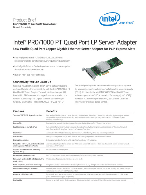
Intel® PRO/1000 PT Quad Port LP Server Adapter Low-Profile Quad Port Copper Gigabit Ethernet Server Adapter for PCI* Express Slots• Four high-performance PCI Express* 10/100/1000 Mbpsconnections for slot-constrained servers requiring high bandwidth• Multi-Gigabit Ethernet Scalability enhances and increases uptimethrough advanced server features• Built on Intel® lead-free1technologyConnectivity You Can Count OnConserve valuable PCI Express (PCIe*) server slots while adding multi-port Gigabit Ethernet capability with the Intel® PRO/1000 PT Quad Port LP Server Adapter. The dedicated input/output (I/O) bandwidth of PCIe ensures priority performance on each port –without bus sharing – for Gigabit Ethernet connectivity in Category-5 networks. The Intel PRO/1000 PT Quad Port LP Server Adapter improves performance in multi-processor systems by balancing network loads across multiple central processing units (CPUs). Additionally, the Intel PRO/1000 PT Quad Port LP Server Adapter supports Intel® I/O Acceleration Technology (Intel® I/OAT)2 for faster I/O processing on the new Quad-Core and Dual-Core Intel® Xeon® processor-based servers.Product BriefIntel® PRO/1000 PT Quad Port LP Server AdapterNetwork ConnectivityFeatures BenefitsTwo Intel® 82571GB Gigabit Controllers Enables four Gigabit Ethernet connections on a single adapter, delivering increased bandwidth for slot-constrained serversand providing high performance, reliability, and low-power use in two single, integrated, dual port PCI Express GigabitEthernet controller chipsLow-profile Enables higher bandwidth and throughput from standard and low-profile PCIe slots and serversLoad balancing on multiple CPUs Increases performance on multi-processor systems by efficiently balancing network loads across CPU cores when usedwith Receive-Side Scaling from Microsoft or Scalable I/O on Linux*Intel® I/OAT2Accelerates I/O with higher throughput and lower CPU utilization by offloading processing overheadVirtualization Multi-port cards provide the platform with the port density required for virtualized environmentsInterrupt moderation Delivers increased performance while significantly reducing CPU utilizationCompatible with x4, x8, and x16 standard Allows quad-port operation in almost any PCI Express server slot, except x1 slots, and allows each port to operate without and low-profile PCI Express* slots interfering with the otherSupport for most network operating Enables widespread deploymentsystems (NOS)Remote management support Reduces support costs with remote management based on industry-wide standardsCategory-5 unshielded twisted pair (UTP), Uses existing 4-pair cabling and saves re-wiring costs4-pair cablingRoHS compliant3, lead-free1technology Compliant with the European Union directive (effective as of July 2006) to reduce the use of hazardous materialsIntel® PROSet Utility for Windows* Provides point-and-click power over individual adapters, advanced adapter features, connection teaming, and Device Managervirtual local area network (VLAN) configurationAdvanced cable diagnostics Dynamically tests and reports network problems (error rate, cable length) and automatically compensates for cable issues(cross-over cable, wrong pin-out/polarity)Intel backing Backed by an Intel® limited lifetime warranty, 90-day money-back guarantee (U.S. and Canada), and worldwide supportSpecificationsGeneralProduct code EXPI9404PTL4Connectors Four RJ-45IEEE standards/network topology10BASE-T, 100BASE-TX,1000BASE-TWiring Category-5, unshielded twistedpair (UTP), 4-pairAdapter Product FeaturesIntel® PROSet Utility and Intel® PRO•Intelligent Install for easy installationIntel® lead-free1technology•Plug and play specification support StandardAuto-negotiation, full-duplex capable•Intel® I/OAT2•Integrated media access control (MAC)•and physical layer (PHY)Includes a full-height bracket•RoHs3•Cable distance100 m in Category-5 for 100/1000Mbps; and Category-3 for 10 Mbps Network ManagementWired for Management (WfM) baseline •v2.0 enabled for serversDMI 2.0 support, Windows Management •Instrumentation (WMI) andSNMP-manageable SMBus supportRemote Installation Services (RIS)•Diagnostics (loopback, testability, •PHY register access)Advanced configuration and power •interface (ACPI) 1.0 power managementWake on LAN* support over PCI Express*•PXE 2.0 enabled through boot read-only•memory (ROM)Network Operating Systems (NOS) Software Support Microsoft Windows* Server 2003, •Enterprise, Datacenter (32- and 64-bit)Microsoft Windows 2000•Red Hat Linux* 2.4x or later (32- and 64-bit)•FreeBSD 4.x or later•Novell Netware*•Sun Solaris* x86, OS 8 and later•SCO Open Server 5, OpenUNIX 8*Intel BackingLimited lifetime warranty•90-day, money-back guarantee•(U.S. and Canada)Advanced Software FeaturesAdapter fault tolerance (AFT)•Switch fault tolerance (SFT)•Adaptive load balancing (ALB)•Fast EtherChannel*5(FEC)•Gigabit EtherChannel*5(GEC)•Teaming support Scales up to 8 connections Multiple teams Supports 4 separate teams,maximumIEEE 802.3ad* (link aggregation •control protocol)5Test switch configuration Tested with major switch originalequipment manufacturers (OEMs) PCIe Hot Plug*/Active peripheral•component interconnect (PCI)IEEE 802.1Q* VLANs•IEEE 802.3* (z, ab, u, x) flow control support•TCP checksum offload — transmission •control protocol (TCP), user datagramprotocol (UDP), Internet protocol (IP)IEEE 802.1p*•TCP segmentation/large send offload•Interrupt moderation•Technical FeaturesData rate(s) supported per port10, 100, and 1000 MbpsBus type PCI Express 1.0aBus width x4 lane PCI Express, operablein x4, x8, x16 slotsBus speed (x4, encoded rate)10 Gbps uni-directional;20 Gbps bi-directional EEPROM-SPI and single EEPROM support•Interrupt levels INTA, INTB, INTC, INTDIEEE support802.3ab*Hardware certifications FCC B, UL, CE, VCCI, BSMI, CTICK, MIC Controller-processor Intel® 82571GBTypical power consumption 4.95 W (3.3 V @ 1.5 A) Operating temperature0–55° CLEDs 4 (1/port, link and speed) solidand blinkingPhysical DimensionsLength16.76 cm (6.6 in)Width 1.91 cm (0.75 in)Height of end bracket 5.97 cm (2.35 in)The Intel PRO/1000 PT Quad Port LP Server Adapter’s low-profile design, the industry’s first server adapter to incorporate four Gigabit Ethernet connections in a low-profile PCI Express slot, improves server throughput and rack density at the same time.The Intel PRO/1000 PT Quad Port LP Server Adapter represents the sixth generation of Intel® network adapters for Gigabit Ethernet, and features 10/100/1000 Mbps self-configuration for compatibility with mixed-speed network infrastructure.For easy installation and management, all Intel® PRO Network Connections are supported by Intel® PRO Intelligent Install andthe new Intel® PROSet Utility for Windows* Device Manager. Intel PROSet simplifies adapter installation and gives you point-and-click power to configure and manage all your Intel PRO Network Connections for connectivity you can count on.Order CodeSingle Unit: EXPI9404PTL4Bulk Pack: EXPI9404PTLBLK (order 5, get 5)Companion ProductsConsider these Intel® products in your server and network planning:• Intel® PRO/1000 Server Adapters– Copper or fiber-optic network connectivity, up to four portsper card– Solutions for PCI Express, PCI-X*, and PCI interfaces• Intel® PRO/10GbE Server Adapters– CX4 offering for cost-effective 10 Gigabit-over-copperconnections– Short-range and long-range connectivity solutions forfiber-optic cabling• Intel® PRO/1000 Desktop Adapters for PCI Expressand PCI interfaces• Other Intel® PRO Desktop and Server Adapters• Intel® Xeon® processors• Intel® Server Boards Network-Ready PCsTop PC and server manufacturers offer Intel® adapters in their new products. Specify or ask for Intel PRO Network Connections with your next PC, server, or mobile PC purchase. For a list of preferred suppliers, visit us at: /network/ connectivity/how_to_buy/index.htm.Customer SupportIntel® Customer Support Services offers a broad selectionof programs including phone support and warranty service.For more information, contact us at / support/network. Service and availability may vary by country.For Product InformationTo speak to a customer service representative regardingIntel products, please call 1-800-538-3373 (U.S. and Canada) or visit /support/9089.htm for the telephone number in your area. For additional product information on Intel® Networking Connectivity products,visit /network/connectivity.To see the full line of Intel® PRO/1000 Network Adapters for PCI Express,visit /network/connectivity1Lead has not been intentionally added, but lead may still exist as an impurity below 1000 ppm, or an approved RoHS exemption applies.2Intel® I/O Acceleration Technology (Intel® I/OAT) requires an operating system that supports Intel I/OAT.3Lead and other materials banned in RoHS Directive are either (1) below all applicable substance thresholds as proposed by the EU or (2) an approved/pending exemption applies. 4Bulk packs also available for minimum order quantities of five adapters. One driver CD per order of five units.5Available only when used with a capable switch.INFORMATION IN THIS DOCUMENT IS PROVIDED IN CONNECTION WITH INTEL®PRODUCTS. EXCEPT AS PROVIDED IN INTEL'S TERMS AND CONDITIONS OF SALE FOR SUCH PRODUCTS, INTEL ASSUMES NO LIABILITY WHATSOEVER, AND INTEL DISCLAIMS ANY EXPRESS OR IMPLIED WARRANTY RELATING TO SALE AND/OR USE OF INTEL PRODUCTS, INCLUDING LIABILITY OR WARRANTIES RELATING TO FITNESS FOR A PARTICULAR PURPOSE, MERCHANTABILITY, OR INFRINGEMENT OF ANY PATENT, COPYRIGHT, OR OTHER INTELLECTUAL PROPERTY RIGHT. INTEL MAY MAKE CHANGES TO SPECIFICATIONS, PRODUCT DESCRIPTIONS, AND PLANS AT ANY TIME, WITHOUT NOTICE.Copyright ©2006 Intel Corporation. All rights reserved.Intel, the Intel logo, Intel. Leap ahead., Intel. Leap ahead. logo, and Xeon are trademarks or registered trademarks of Intel Corporationor its subsidiaries in the United States and other countries.*Other names and brands may be claimed as the property of others.Printed in USA1206/TAR/OCG/XX/PDF Please Recycle315880-002US。
北欧化工直流电缆料

说明 石化设施网路连接,83公里 地面电缆,59公里 整体网络 电站地面连接,42公里 海底风电场连接, 90 公里
高电压,城镇缆线
海底电缆,150公里 机场缆线连接
能源输通世界
高压直流输电电缆 高压直流输电绝缘聚合材料是在 20 世纪 90 年代与电压源换流器技术同时开发 的。在首例商业聚合材料直流输电电缆的聚合绝缘材料和半导体材料的开发方 面,北欧化工居于前沿。2007年 Estlink 联网项目把北欧和波罗的海国家电力 市场相连接,这标志北欧化工在直流输电电缆聚合材料的开发和商业应用方面 10 多年的经验和取得的成功。 北欧化工超净Superclean LE4253 交联聚乙烯材料在无污染的环境下生产,并 通过超净Superclean 纸板箱包装运输,灌装和卸料过程也是在洁净室内进行。 线缆制造商直接受益于产品的洁净程度。焦烧安全性极大提高,降低了绝缘缺 陷的风险,使生产能续更长时间。也减少了脱气时间。 与超净 Superclean LE4253 结合使用的超光滑Supersmooth LE0550 半导体材 料经过设计,把空间电荷积聚降到最低程度。产品极为光滑,为导体和绝缘屏 蔽都提供了平整表面,并减少了应力。产品经过设计,适合地下和海底 运行环境。超净 Superclean交联绝缘线缆安装快速,对环境的负面影响小,为 配电商提供了保障。
低压电缆的巨大需求使制造商面临着更高的要求和更激烈的竞争。成本效率和 高价值解决方案对于其在业界的生存至关重要。正因为有如此高的标准,没有 其他任何温水交联聚乙烯解决方案能比 Visico/Ambicat 提供更高的生产效率和 产量。
由于Visico 基础树脂在反应釜内直接制造 (reactor-made),质量高,性能稳定。 焦烧性能无与伦比,可连续生一个月, 且不需清洁挤出机。和 Visico 组合使用的 Ambicat 催化剂使用环保的磺酸作为活性物质,不含有害的有机锡添加剂。而 且交联速度大大提高。
UPSilon系列STS彩页中文版

增强安全性和可维护性
MGE Upsilon™ STS可在不中断被保护负载供电的情况下, 对需要维护的线路进行隔离。其具有安全保护功能,包 括采用机械连动装置的旁路开关、可钥匙锁定的负载隔 离开关,以及采用密码保护的手动切换。
本手册采用生态纸印刷
施耐德电气信息技术(中国)有限公司
北京 中国北京市朝阳区望京东路 6 号 施耐德电气大厦 电话:86 (10) 8434 6699 传真:86 (10) 6431 5686 邮编:100102
沈阳 中国沈阳市和平区和平北大街 69 号 总统大厦 A 座 1902 室 电话:86 (24) 2281 5008 传真:86 (24) 2281 5783 邮编:110003
MGETM UpsilonTM STS 的功能
便于操作
● STS的LCD图形显示界面支持多语种显示功能,可快速读取测量值并直接设置参数。 ● 前面板上显示直观的模拟图,实时了解电能流向及系统状态。 ● 提供详细的旁路操作流程图。 ● 提供专用端子,用于假负载测试。
● Jbus/ModBus串行接口卡可提供一个PC接口,干接点通信卡则具备可编程远程监测功 能,另外,选配的XML网卡支持以太网通讯。
< 60 dB
IEC 60950 ,GR-63-CORE IEC 61000-6-4 , IEC 61000-6-2 ,EN55011
TÜV , CE
1430 x 610 or 1900 x 715 550 825
193 215
211 225
1900 x 715 -
PT6314中文资料
100
90
Vin
80
9.0V
12.0V
70
15.0V
20.0V
26.0V
60
50
40
0
0.5
1
1.5
2
2.5
3
Iout-(Amps)
Efficiency - %
Efficiency vs Output Current
100
90
80
70
60
50
40
0
0.5
1
1.5
2
2.5
3
Iout-(Amps)
Vin
2
2.5
3
Iout-(Amps)
Iout-(Amps)
Thermal Derating (Ta)
3
2.5
(See Note B)
60°C 70°C
2
85°C
1.5
1
0.5
0
9
11 13 15 17 19 21 23 25 27
Vin-(Volts)
Iout-(Amps)
Thermal Derating (Ta)
元器件交易网
PT6300 Series
3 Amp Adjustable Positive Step-down Integrated Sw itching Regulators
SLTS031B
(Revised 9/30/2000)
• 90% Efficiency • Adjustable Output Voltage • Internal Short Circuit Protection • Over-Temperature Protection • On/Off Control (Ground Off) • Small SIP Footprint • Wide Input Range
6N134中文资料

6N134中⽂资料FeaturesDual Marked with Device Part Number and DSCC Drawing NumberManufactured and Tested on a MIL-PRF-38534 Certified LineQML-38534, Class H and K Five Hermetically Sealed Package Configurations Performance Guaranteed over -55°C to +125°C ? High Speed: 10 M Bit/sCMR: > 10,000 V/µs Typical 1500 Vdc Withstand Test Voltage2500 Vdc Withstand Test Voltage for HCPL-565X High Radiation Immunity 6N137, HCPL-2601, HCPL-2630/-31 Function Compatibility ? Reliability DataTTL Circuit CompatibilityApplicationsMilitary and SpaceHigh Reliability SystemsTransportation, Medical, and Life Critical SystemsLine ReceiverVoltage Level ShiftingIsolated Input Line Receiver Isolated Output Line Driver Logic Ground Isolation Harsh Industrial EnvironmentsIsolation for Computer,Communication, and Test Equipment SystemsDescriptionThese units are single, dual and quad channel, hermetically sealed optocouplers. The products are capable of operation and storage over the full military temperature range and can be purchased as either standard product or with full MIL-PRF-38534 Class Level H or K testing or from the appropri-ate DSCC Drawing. All devices are manufactured and tested on a MIL-PRF-38534 certified line and are included in the DSCC Quali-fied Manufacturers List QML-38534 for Hybrid Microcircuits.Quad channel devices areavailable by special order in the 16 pin DIP through hole packages.Truth Table(Positive Logic)Multichannel DevicesInput Output On (H)L Off (L)HFunctional DiagramMultiple Channel Devices AvailableSingle Channel DIP Input Enable Output On (H)H L Off (L)H H On (H)L H Off (L)LH*See matrix for available extensions.Hermetically Sealed, High Speed,High CMR, Logic Gate Optocouplers Technical Data6N134*81028HCPL-563X HCPL-663X HCPL-565X 5962-98001HCPL-268K HCPL-665X 5962-90855HCPL-560XCAUTION: It is advised that normal static precautions be taken in handling and assembly of this component to prevent damage and/or degradation which may be induced by ESD.V CC V OUTV E GNDThe connection of a 0.1 µF bypass capacitor between V CC and GND is recommended.Selection Guide–Package Styles and Lead Configuration OptionsPackage16 Pin DIP 8 Pin DIP 8 Pin DIP 8 Pin DIP 16 Pin Flat Pack 20 Pad LCCC Lead Style Through Hole Through Hole Through Hole Through Hole Unformed Leads Surface MountChannels 212242Common Channel V CC , GND None V CC , GND V CC , GND V CC , GND None WiringWithstand Test Voltage 1500 Vdc 1500 Vdc 1500 Vdc 2500 Vdc 1500 Vdc 1500 Vdc Agilent Part # & Options Commercial6N134*HCPL-5600HCPL-5630HCPL-5650HCPL-6650HCPL-6630MIL-PRF-38534, Class H 6N134/883BHCPL-5601HCPL-5631HCPL-5651HCPL-6651HCPL-6631MIL-PRF-38534, Class K HCPL-268K HCPL-560K HCPL-563K HCPL-665K HCPL-663K Standard Lead Finish Gold Plate Gold Plate Gold Plate Gold Plate Gold PlateSolder PadsSolder Dipped Option #200Option #200Option #200Option #200Butt Cut/Gold Plate Option #100Option #100Option #100Gull Wing/Soldered Option #300Option #300Option #300Class H SMD Part #Prescript for all below None 5962-None None None None Either Gold or Solder 8102801EX 9085501HPX 8102802PX 8102805PX 8102804FX 81028032XGold Plate 8102801EC 9085501HPC 8102802PC 8102805PC 8102804FCSolder Dipped 8102801EA 9085501HPA 8102802PA 8102805PA81028032A Butt Cut/Gold Plate 8102801UC 9085501HYC 8102802YC Butt Cut/Soldered 8102801UA 9085501HYA 8102802YA Gull Wing/Soldered 8102801TA 9085501HXA8102802ZA Class K SMD Part #Prescript for all below 5962-5962-5962-5962-5962-Either Gold or Solder 9800101KEX 9085501KPX 9800102KPX 9800104KFX 9800103K2XGold Plate 9800101KEC 9085501KPC 9800102KPC 9800104KFCSolder Dipped 9800101KEA 9085501KPA 9800102KPA 9800103K2AButt Cut/Gold Plate 9800101KUC 9085501KYC 9800102KYC Butt Cut/Soldered 9800101KUA 9085501KYA 9800102KYA Gull Wing/Soldered9800101KTA 9085501KXA 9800102KZA*JEDEC registered part.Each channel contains a GaAsP light emitting diode which isoptically coupled to an integrated high speed photon detector. The output of the detector is an open collector Schottky clamped transistor. Internal shields provide a guaranteed common mode transient immunityspecification of 1000 V/µs. For Isolation Voltage applications requiring up to 2500 Vdc, the HCPL-5650 family is also available. Package styles for these parts are 8 and 16 pin DIP through hole (case outlines P andE respectively), and 16 pin surface mount DIP flat pack(case outline F), leadless ceramic chip carrier (case outline 2).Devices may be purchased with a variety of lead bend and plating options. See Selection Guide Table for details. Standard Microcircuit Drawing (SMD)parts are available for each package and lead style.Because the same electrical die (emitters and detectors) are used for each channel of each device listed in this data sheet, absolute maximum ratings, recommended operating conditions, electrical specifications, and performance characteristics shown in the figures are identical for all parts.Occasional exceptions exist due to package variations and limitations,and are as noted. Additionally, the same package assembly processes and materials are used in all devices. These similarities give justification for the use of data obtained from one part torepresent other parts’ performance for reliability and certain limited radiation test results.Outline Drawings16 Pin DIP Through Hole, 2 ChannelsFunctional DiagramsNote: All DIP and flat pack devices have common V CC and ground. Single channel DIP has an enable pin 7. LCCC (leadless ceramic chip carrier) package has isolated channels with separate VCC and ground connections. All diagrams are “top view.”Leaded Device MarkingLeadless Device MarkingNOTE: DIMENSIONS IN MILLIMETERS (INCHES).COMPLIANCE INDICATOR,*DATE CODE, SUFFIX (IF NEEDED)COUNTRY OF MFR.Agilent CAGE CODE*Agilent DESIGNATORDSCC SMD*PIN ONE/ ESD IDENTAgilent P/N DSCC SMD** QUALIFIED PARTS ONLYCOMPLIANCE INDICATOR,*DATE CODE, SUFFIX (IF NEEDED)DSCC SMD*Agilent CAGE CODE*Agilent DESIGNATORCOUNTRY OF MFR.Agilent P/N PIN ONE/ ESD IDENTDSCC SMD** QUALIFIED PARTS ONLYOutline Drawings (continued)16 Pin Flat Pack, 4 Channels8 Pin DIP Through Hole, 2 Channels 2500 Vdc Withstand Test Voltage20 Terminal LCCC Surface Mount,2Channels8 Pin DIP Through Hole, 1 and 2 Channels0.36 (0.014)NOTE: DIMENSIONS IN MILLIMETERS (INCHES).2.29 (0.090) 2.79 (0.110)NOTE: DIMENSIONS IN MILLIMETERS (INCHES).NOTE: DIMENSIONS IN MILLIMETERS (INCHES).NOTE: DIMENSIONS IN MILLIMETERS (INCHES). SOLDER THICKNESS 0.127 (0.005) MAX.Hermetic Optocoupler OptionsRecommended Operating ConditionsParameterSymbol Min.Max.Units Input Current, Low Level, Each Channel I FL 0250µA Input Current, High Level, Each Channel*I FH 1020mA Supply Voltage, OutputV CC 4.55.5VFan Out (TTL Load) Each ChannelN6*Meets or exceeds DSCC SMD and JEDEC requirements.Absolute Maximum Ratings(No derating required up to +125°C)Storage Temperature Range, T S ...................................-65°C to +150°C Operating Temperature, T A..........................................-55°C to +125°C Case Temperature, T C ................................................................+170°C Junction Temperature, T J ...........................................................+175°C Lead Solder Temperature ...............................................260°C for 10 s Peak Forward Input Current, I F PK , (each channel,≤1 ms duration)......................................................................40 mA Average Input Forward Current, I F AVG (each channel)................20 mA Input Power Dissipation (each channel).....................................35 mW Reverse Input Voltage, V R (each channel).........................................5 V Supply Voltage, V CC (1 minute maximum)........................................7 V Output Current, I O (each channel)...............................................25 mA Output Power Dissipation (each channel). (40)mW Output Voltage, V O (each channel)..................................................7 V*Package Power Dissipation, P D (each channel)........................200 mW*Selection for higher output voltages up to 20 V is available.Single Channel Product OnlyEmitter Input Voltage, V E ...............................................................5.5 VNote enable pin 7. An external 0.01 µF to 0.1 µF bypass capacitor must be connected between V CC and ground for each package type.8 Pin Ceramic DIP Single Channel SchematicESD Classification(MIL-STD-883, Method 3015)HCPL-5600/01/0K ...............................................................(?), Class 16N134, 6N134/883B, HCPL-5630/31/3K, HCPL-5650/51, HCPL-6630/31/3K and HCPL-6650/51/5K.......................(Dot), Class 3Electrical Characteristics (T= -55°C to +125°C, unless otherwise specified)*Identified test parameters for JEDEC registered parts.**All typical values are at V CC = 5 V , T A = 25°C. Recommended Operating Conditions (cont’d.)Single Channel Product Only [10]ParameterSymbol Min.Max.Units High Level Enable Voltage V EH 2.0V CC V Low Level Enable VoltageV EL0.8VElectrical Characteristics, (Contd.) T= -55°C to +125°C unless otherwise specifiedSingle Channel Product Only Low Level I EL V CC = 5.5 V,1, 2, 3-1.45-2.0mA Enable Current V E = 0.5 V High Level V EH 1, 2, 3 2.0V10Enable Voltage Low Level V EL 1, 2, 30.8VEnable Voltage*Identified test parameters for JEDEC registered part.**All typical values are at V CC = 5 V , T A = 25°C.Typical Characteristics, T = 25°C, V = 5 VDual and Quad Channel Product Only Input-Input I I-I 0.5nA Relative Humidity = 45%4Leakage CurrentV I-I = 500 V, t = 5 s Resistance (Input-Input)R I-I 1012V I-I = 500 V 4Capacitance (Input-Input)C I-I0.55pF f = 1 MHz4Notes:1. Each channel.2. All devices are considered two-terminal devices; I I-O is measured between all input leads or terminals shorted together and alloutput leads or terminals shorted together.3. Measured between each input pair shorted together and all output connections for that channel shorted together.4. Measured between adjacent input pairs shorted together for each multichannel device.5. t PHL propagation delay is measured from the 50% point on the leading edge of the input pulse to the 1.5 V point on the leadingedge of the output pulse. The t PLH propagation delay is measured from the 50% point on the trailing edge of the input pulse to the1.5 V point on the trailing edge of the output pulse.6. The HCPL-6630, HCPL-6631, and HCPL-663K dual channel parts function as two independent single channel units. Use the singlechannel parameter limits for each channel.7. CM L is the maximum rate of rise of the common mode voltage that can be sustained with the output voltage in the logic low state(V O < 0.8 V). CM H is the maximum rate of fall of the common mode voltage that can be sustained with the output voltage in the logic high state (V O > 2.0 V).8. This is a momentary withstand test, not an operating condition.9. It is essential that a bypass capacitor (0.01 to 0.1 µF, ceramic) be connected from V CC to ground. Total lead length between bothends of this external capacitor and the isolator connections should not exceed 20 mm.10. No external pull up is required for a high logic state on the enable input.11. The t ELH enable propagation delay is measured from the 1.5 V point on the trailing edge of the enable input pulse to the 1.5 Vpoint on the trailing edge of the output pulse.12. The t EHL enable propagation delay is measured from the 1.5 V point on the leading edge of the enable input pulse tothe 1.5 Vpoint on the leading edge of the output pulse.13. Standard parts receive 100% testing at 25°C (Subgroups 1 and 9). SMD and 883B parts receive 100% testing at 25, 125, and-55°C (Subgroups 1 and 9, 2 and 10, 3 and 11, respectively).14. Parameters are tested as part of device initial characterization and after design and process changes. Parameters are guaranteedto limits specified for all lots not specifically tested.15. Not required for 6N134, 6N134/883B, 8102801, HCPL-268K and 5962-9800101 types.16. Required for 6N134, 6N134/883B, 8102801, HCPL-268K and 5962-9800101 types.17. Not required for HCPL-5650, HCPL-5651 and 8102805 types.18. Required for HCPL-5650, HCPL-5651 and 8102805 types only.Figure 1. High Level Output Currentvs. Temperature.5 VV O * C L INCLUDES PROBE AND STRAY WIRING CAPACITANCE. Figure 4. Test Circuit for t PHL and t PLH .*I +5 V OUTPUT V O MONITORING NODEFigure 7. Test Circuit for Common Mode Transient Immunity and Typical Waveforms.11OUTPUT V OMONITORINGNODET A = +125 °C* ALL CHANNELS TESTED SIMULTANEOUSLY.V CCI O = 25 mAFigure 10. Operating Circuit for Burn-In and Steady State Life Tests. Figure 8. Test Circuit for t EHL and t ELH.Figure 9. Enable Propagation Delayvs. Temperature.MIL-PRF-38534 Class H,Class K, and DSCC SMDTest ProgramAgilent’s Hi-Rel Optocouplers arein compliance with MIL-PRF-38534 Classes H and K. Class Hand Class K devices are also incompliance with DSCC drawings81028, 5962-90855 and 5962-98001.Testing consists of 100% screen-ing and quality conformanceinspection to MIL-PRF-38534./doc/4e2d970a03d8ce2f006623a8.htmlData subject to change.Copyright ? 1999 Agilent TechnologiesObsoletes 5968-4743E5968-9407E (10/00)。
普源rogal示波器中文手册
特有的内置函数/任意波形发生器模块
■ 业界第一个嵌入到数字存储示波器的函数/任意波形发生器模块 ■ 采用先进的DDS技术,得到精确、稳定、低失真的输出信号 ■ 200MSa/S采样率,12bits垂直分辨率 ■ 10MHz / 20MHz / 40MHz正弦波/方波信号最高频率 ■ 10MHz的脉冲信号最高频率 ■ 内置最高频率为1MHz的三角波、抽样函数、梯形波等30种常用波形 ■ 内置AM、FM、PWM、FSK、PSK和偏置调制等丰富的调制功能 ■ 1u~10MHz/1u~20MHz/1u~40MHz的扫频,可以正向扫描、
图9 X-Y模式测量李沙育图形 图10 视频触发测量全电视信号
更多功能
数字滤波器 仪器提供多种数字滤波器选择,包括低通、高通、带通和带阻滤 波器。您可以对采集信号按要求进行滤波处理以获得希望的结果。 可以利用数字滤波器来模拟硬件滤波的效果;利用数字滤波器滤 除混叠的噪声或误差信号以清楚地观察感兴趣的信号等。 可任意设定所需数字滤波器的3dB上限或下限截止频率。
卓越的信号观察能力
观察信号更清晰 TDO3000A/B系列使用明亮、清晰的分辨率为320 × 234点阵的5.6英 寸彩色TFT LCD显示器,您几乎可以从任何角度快速地观察信号。与 需要一直打开菜单的传统示波器不同,TDO3000A/B的整个5.6英寸 显示屏可以根据需要用于波形显示。 单键MENU ON/OFF可在更大的显示区域看到更多信号信 息,选择关闭菜单时可增加接近25%的显示面积。
距屏幕中心±8格
×1,×10,×100,×1000
1MΩ||18pF
两个通道刻度和耦合设置相同的时候±150ps
400V(DC+AC峰值,@1MΩ)
PT5504中文资料
mV µSec mV A kHz V mA µF °C °C G’s G’s grams
— —
Notes: (1) The ISR will operate down to no load with reduced specifications. (2) This is a typical value only. The switching frequency will vary with input voltage. (3) The Inhibit control (pin 1) has an internal pull-up, and if left open-circuit the module will operate when input power is applied. A small low-leakage (<100nA) MOSFET is recommended to control this input. Ensure an On/Off transition time of ≤ 10µs. See application notes for more information. (4) The PT5500 Series requires a 100µF electrolytic or tantalum output capacitor for proper operation in all applications. (5) For operation below 0°C, the output capacitor C2 must have stable characteristics. Use either a low ESR tantalum or Oscon® capacitor. (6) See SOA curves or consult factory for the appropriate derating. (7) The case pins on the through-hole package types (suffixes N & A) must be soldered. For more information see the applicable package outline drawing.
EPI6L2172KSP45L中文资料

TEL: (818) 892-0761 FAX: (818) 894-5791
---
54
---
40
---
34
---
35
---
40
42
---
38
---
34
---
37
---
37
---
37
---
40
---
Package B20
.330 (8.83)
PCA EPIXXXXXXB20
D.C.
.330 (8.38)
.060 (1.52)
.300 (7.62)
Suggested Pad Latout
元器件交易网
Surface Mount Power Inductor
ELECTRONICS INC.
EPI B30 Series
• Optimized for National’s LM259X Series • Low loss material ensures operation in high frequency switching
converters, such as Buck, Boost or as output averaging filter inductor • Also suitable for use in high quality filter applications • 150 KHz & 500 KHz Switching Frequency • Low Cost Inductor
PT6964中文资料
PT6964 is an LED Controller driven on a 1/7 to 1/8 duty factor. 10 segment output lines, 4 grid output lines, 3 segment/ grid output lines, one display memory, control circuit, key scan circuit are all incorporated into a single chip to build a highly reliable peripheral device for a single chip microcomputer. Serial data is fed to PT6964 via a three-line serial interface. Housed in a 28 pins SO Package, PT6964 pin assignments and application circuit are optimized for easy PCB Layout and cost saving advantages.FEATURES• CMOS Technology•Low Power Consumption•Multiple Display Modes (10 segment, 7 Grid to 13 segment, 4 Grid)•Key Scanning (10 x 2 Matrix)•8-Step Dimming Circuitry•Serial Interface for Clock, Data Input, Data Output, Strobe Pins•Available in 28 pins, SOPAPPLICATIONS•Micro-computer Peripheral Device• VCR set• Combo setLED Driver IC PT6964PIN DESCRIPTIONSG8/KS81 3 2 5 4 8 7 6 10 9 12 11 PT696428 26 27 2425 21 22 2319 20 17181413 15 16OSC DI/O CLK STB K1K2VDD SG1/KS1SG2/KS2SG3/KS3SG4/KS4SG5/KS5SG6/KS6SG7/KS7SG9/KS9SG10/KS10GND GR1GR2GND GR3GR4GND VDD SG14/GR5SG13/GR6SG12/GR7APPLICATION CIRCUITNote:1. The capacitor (0.1µF) connected between the GND and the VDD pins must be located as close as possible to the PT6964 chip.2. It is strongly suggested that the NC pin (pins 13) be connected to the GND.3. The PT6964 power supply is separate from the application system power supply.COMMON CATHODE TYPE LED PANELValid Part Number Package Type Top CodePT6964-S 28pins, SOP, 300mil PT6964-SPT6964-S (L) 28pins, SOP, 300mil PT6964-SNotes:1. (L) = Lead Free2. The Lead Free mark is put in front of the date code.。
L6599_中文资料
L6599高压谐振控制器特征50%占空比,谐振半桥变频控制 高精度振荡器高至500kHz 的工作频率 序号编码器件编码封 装包 装L6599D SO-16N 管装 L6599DTR SO-16N 卷带 L6599NDIP16管装两级过流保护:变频和停机闭锁 与PFC 控制器的接口 自锁禁止输入 轻载脉冲工作模式上电/断电顺序或欠压保护输入 单调输出电压上升为非线性软启动整合了一个能够承受600V 以上电压的高压浮动结构和一个同步驱动式高压横向双扩散金属氧化物半导体(LDMOS)器件,节省了一个外部快速恢复自举二极管用低电压下拉方式为两个栅驱动器提供一个输出电流0.3A 和灌入电流0.8A的典型峰值电流处理能力。
DIP-16,SO-16N 两种封装特征液晶电视和等离子电视的电源 台式电脑和初级服务器 电信设备开关电源 交直流适配器的开关电源框图目录1 驱动描述 . . . . . . . . . . . . . . . . . . . . . . . . . . . . . . . . . . . . . . . . . . . . . . . . . .42 引脚设置 . . . . . . . . . . . . . . . . . . . . . . . . . . . . . . . . . . . . . . . . . . . . . . . . . .52.1 引脚排列 . . . . . . . . . . . . . . . . . . . . . . . . . . . . . . . . . . . . . . . . . . . . . . . . . . . .52.2 引脚功能说明 . . . . . . . . . . . . . . . . . . . . . . . . . . . . . . . . . . . . . . . . . . . . . . . . 53 典型系统框图 . . . . . . . . . . . . . . . . . . . . . . . . . . . . . . . . . . . . . . . . . . . . . . 74 电气数据 . . . . . . . . . . . . . . . . . . . . . . . . . . . . . . . . . . . . . . . . . . . . . . . . . . 74.1 极限参数. . . . . . . . . . . . . . . . . . . . . . . . . . . . . . . . . . . . . . . . . . . . . . . . . . . . . .74.2 热相关数据. . . . . . . . . . . . . . . . . . . . . . . . . . . . . . . . . . . . . . . . . . . . . . . . . . . . .85 电气参数. . . . . . . . . . . . . . . . . . . . . . . . . . . . . . . . . . . . . . . . . . . . . . . . . . . 96 典型的电气性能. . . . . . . . . . . . . . . . . . . . . . . . . . . . . . . . . . . . . . . . . . . . . .127 应用资料. . . . . . . . . . . . . . . . . . . . . . . . . . . . . . . . . . . . . . . . . . . . . . . . . . . 157.1 振荡器. . . . . . . . . . . . . . . . . . . . . . . . . . . . . . . . . . . . . . . . . . . . . . . . . . . . . . .167.2 工作在空载或非常轻的负载状态. . . . . . . . . . . . . . . . . . . . . . . . . . . . . . . . . . .187.3 软启动. . . . . . . . . . . . . . . . . . . . . . . . . . . . . . . . . . . . . . . . . . . . . . . . . . . . . . . .217.4 电流检测,过流保护和过载保护 . . . . . . . . . . . . . . . . . . . . . . . . . . . . . . . . . 237.5 闭锁关机. . . . . . . . . . . . . . . . . . . . . . . . . . . . . . . . . . . . . . . . . . . . . . . . . . . . . .267.6 LINE检测功能. . . . . . . . . . . . . . . . . . . . . . . . . . . . . . . . . . . . . . . . . . . . . . . . . .277.7 自举部分 . . . . . . . . . . . . . . . . . . . . . . . . . . . . . . . . . . . . . . . . . . . . . . . . . . . .287.8 应用实例. . . . . . . . . . . . . . . . . . . . . . . . . . . . . . . . . . . . . . . . . . . . . . . . . . . . .298 封装外形尺寸 . . . . . . . . . . . . . . . . . . . . . . . . . . . . . . . . . . . . . . . . . . . . . . . . .9 修订记录 . . . . . . . . . . . . . . . . . . . . . . . . . . . . . . . . . . . . . . . . . . . . . . . . . . . .1 驱动描述L6599是一个用于谐振半桥拓扑电路的精确的双端控制器。
PT6304N;PT6304A;PT6303C;PT6304C;PT6303N;中文规格书,Datasheet资料
30.0V
24.0V
100
15.0V
12.0V
80
9.0V
60
40
20
0
0
0.5
1
1.5
2
2.5
3
Iout-(Amps)
Ripple-(mV)
Ripple vs Output Current
350
300
250
Vin
38.0V
200
30.0V
24.0V
150
20.0V
16.0V
100
50
0
0
0.5
1
1.5
Quiescent current in the shutdown mode is typically less than 100µA.
Standard Application
VOADJ
12
VIN
2,3,4
PT6300
9,10,11
VOUT
1
C1 INH
COM
5,6,7,8
+ C2
Q1
COM
C1 = Optional 1µF ceramic C2 = Required 100µF electrolytic (1) Q1 = NFET
Output Voltage Tolerance
Line Regulation Load Regulation Vo Ripple/Noise Transient Response with Co = 100µF Efficiency
Symbols Io Isc Vin
∆Vo
Regline Regload Vn ttr Vos η
PT6964-S中文资料

PT6964 is an LED Controller driven on a 1/7 to 1/8 duty factor. 10 segment output lines, 4 grid output lines, 3 segment/ grid output lines, one display memory, control circuit, key scan circuit are all incorporated into a single chip to build a highly reliable peripheral device for a single chip microcomputer. Serial data is fed to PT6964 via a three-line serial interface. Housed in a 28 pins SO Package, PT6964 pin assignments and application circuit are optimized for easy PCB Layout and cost saving advantages.FEATURES• CMOS Technology•Low Power Consumption•Multiple Display Modes (10 segment, 7 Grid to 13 segment, 4 Grid)•Key Scanning (10 x 2 Matrix)•8-Step Dimming Circuitry•Serial Interface for Clock, Data Input, Data Output, Strobe Pins•Available in 28 pins, SOPAPPLICATIONS•Micro-computer Peripheral Device• VCR set• Combo setLED Driver IC PT6964PIN DESCRIPTIONSG8/KS81 3 2 5 4 8 7 6 10 9 12 11 PT696428 26 27 2425 21 22 2319 20 17181413 15 16OSC DI/O CLK STB K1K2VDD SG1/KS1SG2/KS2SG3/KS3SG4/KS4SG5/KS5SG6/KS6SG7/KS7SG9/KS9SG10/KS10GND GR1GR2GND GR3GR4GND VDD SG14/GR5SG13/GR6SG12/GR7APPLICATION CIRCUITNote:1. The capacitor (0.1µF) connected between the GND and the VDD pins must be located as close as possible to the PT6964 chip.2. It is strongly suggested that the NC pin (pins 13) be connected to the GND.3. The PT6964 power supply is separate from the application system power supply.COMMON CATHODE TYPE LED PANELValid Part Number Package Type Top CodePT6964-S 28pins, SOP, 300mil PT6964-SPT6964-S (L) 28pins, SOP, 300mil PT6964-SNotes:1. (L) = Lead Free2. The Lead Free mark is put in front of the date code.。
PT6554LQ中文资料
Fax: 886-2-29174598URL: LCD Driver IC PT6554 DESCRIPTIONPT6554 is a high performance Liquid Crystal Display (LCD) Driver IC utilizing CMOS Technology specially designed with Key Input Function. It can drive up to a maximum of 164 segments and control up to 4 general purpose output ports. It includes a Key Scan Circuit that can support up to 30 key inputs and provides On-Chip Voltage Detection Type Reset Circuit which prevents incorrect display. Display Data can be directly displayed without using any decoder. PT6554 also supports both 1/4 duty-1/2 bias and 1/4 duty-1/3 bias drive techniques. Pin assignments and application circuit are optimized for easy PCB Layout and cost saving advantages.FEATURES• CMOS Technology•Up to 164 Segment Drivers (4 Com x 41 Seg)•Up to 4 General Purpose Output Ports•Key Input Function•1/4 Duty-1/2 Bias and 1/4 Duty-1/3 Bias Drive Techniques•Sleep Mode & All Segment OFF Function•On-Chip Voltage Detection Type Reset Circuit•RC Oscillation Circuit•Available in 64 pins, QFP or LQFP PackageAPPLICATION•Electronic Equipment with LCD DisplayFax: 886-2-29174598URL: LCD Driver IC PT6554 PIN CONFIGURATIONFax: 886-2-29174598URL: LCD Driver IC PT6554 APPLICATION CIRCUIT 1Notes: 1. A capacitor must be added to the power line so that both the power supply voltage (VDD) rise time when power is applied and the power supply voltage (VDD) fall timewhen power drops are at least 1 ms.2.DO is an open - drain output and requires a pull-high resistor between 1kΩ to 10kΩ.The pull-up resistor value must be appropriate to the capacitor of the external wiring sothat the signal wave forms are not degraded.Fax: 886-2-29174598URL: LCD Driver IC PT6554 APPLICATION CIRCUIT 2Notes: 1. A capacitor must be added to the power line so that both the power supply voltage (VDD) rise time when power is applied and the power supply voltage (VDD) fall timewhen power drops are at least 1 ms.2.DO is an open - drain output and requires a pull-high resistor between 1kΩ to 10kΩ.The pull-up resistor value must be appropriate to the capacitor of the external wiring sothat the signal wave forms are not degraded.Fax: 886-2-29174598URL: LCD Driver IC PT6554 APPLICATION CIRCUIT 3Notes: 1. A capacitor must be added to the power line so that both the power supply voltage (VDD) rise time when power is applied and the power supply voltage (VDD) fall timewhen power drops are at least 1 ms.2.DO is an open-drain output and requires a pull-high resistor between 1kΩ to 10kΩ.The pull-up resistor value must be appropriate to the capacitor of the external writing sothat the signal wave forms are not degraded.3. R1=R2=R3, the resistance value must be decide by the LCD panel size.Fax: 886-2-29174598URL: LCD Driver IC PT6554 ORDER INFORMATIONOrder Part Number Package Type Top CodePT6554 64 Pin QFP Package PT6554PT6554LQ 64 Pin LQFP Package PT6554LQPT6554 (L) 64 Pin QFP Package PT6554PT6554LQ (L) 64 Pin LQFP Package PT6554LQNotes:1. (L) = Lead Free2. The Lead Free mark is put in front of the date code.。
LT6551中文资料
q q q
MIN 40 3 35 25
TYP 48 50 8.5
MAX
UNITS dB V mA mA
10 11
mA mA V/µs V/µs MHz MHz dB ns ns % % Deg dB
Slew Rate (Note 8) Small Signal –3dB Bandwidth Gain Flatness Gain Matching Settling Time to 3% Settling Time to 1% % Overshoot Differential Gain Differential Phase Channel Separation
Output Voltage Swing Low
Output Voltage Swing High
2
U
U
W
W W U
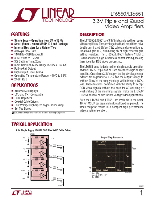
W
TOP VIEW IN1 IN2 IN3 IN4 GND 1 2 3 4 5
X2 X2 X2 X2
ORDER PART NUMBER
10 9 8 7 6 VCC OUT1 OUT2 OUT3 OUT4
The LT®6550/LT6551 are 3.3V triple and quad high speed video amplifiers. These voltage feedback amplifiers drive double terminated 50Ω or 75Ω cables and are configured for a fixed gain of 2, eliminating six or eight external gain setting resistors. The LT6550/LT6551 feature 110MHz –3dB bandwidth, high slew rates and fast settling, making them ideal for RGB video processing. The LT6551 quad is designed for single supply operation and the LT6550 triple can be used on either single or split supplies. On a single 3.3V supply, the input voltage range extends from ground to 1.55V and the output swings to within 400mV of the supply voltage while driving a 150Ω load. These features, combined with the ability to accept RGB video signals without the need for AC coupling or level shifting of the incoming signals, make the LT6550/ LT6551 an ideal choice for low voltage video applications. Both the LT6550 and LT6551 are available in the small 10-Pin MSOP package and utilize a flow-thru pin out. The small footprint results in a compact high performance video amplifier solution.
ptp4l使用
ptp4l使⽤ptp4l是关于1588v2 ptp协议栈的开源代码,其中实现了各种ITU 规定的profile. ITU规定的各种profile主要满⾜电信要求的⼀些profile, profile 的定义请参看1588v2协议。
Ptp4l实现了BC时钟和OC时钟. 本⽂主要分析ptp4l的开源代码。
ptp4l的使⽤⼿册 .语法:ptp4l [ -A | -E | -P ] [ -2 | -4 | -6 ] [ -H | -S | -L ] [ -f config ] [ -p phc-device ] [ -s ] [ -l print-level ] [ -q ] [ -v ] [ -i interface ] ...选项-A ⾃动选择延迟机制,初始为E2E,当收到对端的delay request的时候切换到P2P.-E 选择延迟请求-响应机制E2E。
默认机制-P 选择对端延迟机制P2P.-2 IEEE802.3⽹络传输-4 UDP IPv4传输默认值-6 UDP IPv6 传输-H 硬件打时间戳-S 软件打时间戳-L legacy硬件时间戳-f config 读取配置⽂件-p phc设备,硬件时间戳的设备 /dev/ptp0-s 只作为从时钟-l 打印级别,级别是根据syslog定义的。
默认为6 LOG_INFO-q 不打印消息到系统⽇志-v 打印消息的标准输出-i interface 确定⼀个ptp的端⼝。
-h 显⽰帮助信息配置⽂件配置⽂件分为⼏个部分,每个部分的前⾯都是中括号包含名字,后⾯每⼀⾏都是名字和相应的设置组成。
空⾏和以#开头的⾏忽略。
全局配置部分[global]设置程序的参数,时钟的参数,和端⼝的参数。
其他的部分是端⼝特有的,端⼝特头的设置会覆盖默认全局的设置。
端⼝的设置部分以端⼝的名字开头,例如[eth0].端⼝参数选项logAnnounceIntervalAnnounce消息的平均时间间隔。
SIGLENT SDS6000 Pro 系列数字示波仪数据手册(中文版)说明书

数据手册CN03ASDS6204 H12 Pro / SDS6204 H10 Pro SDS6104 H12 Pro / SDS6104 H10 Pro SDS6054 H12 Pro / SDS6054 H10 Pro SDS6034 H12 Pro / SDS6034 H10 Pro SDS6208 H12 Pro / SDS6208 H10 Pro SDS6108 H12 Pro / SDS6108 H10 Pro SDS6058 H12 Pro / SDS6058 H10 Pro产品综述SDS6000 Pro系列高分辨率数字示波器,具有最高12-bit垂直分辨率、优秀的本底噪声性能和垂直测量精度,能满足更高精度的测量需求。
SDS6000 Pro的最大带宽2 GHz,采样率最高10 GSa/s,具备最多8个模拟通道和16个数字通道,存储深度可达500 Mpts/通道。
SDS6000 Pro采用的SPO 技术,波形捕获率高达750 000帧/秒,具有256级辉度等级及色温显示;创新的数字触发系统,触发灵敏度高,触发抖动小;支持丰富的智能触发、串行总线触发和解码;支持历史(History)模式、分段采集(Sequence)、模板测试、搜索、导航、波形直方图、波特图、电源分析、眼图和抖动分析等高级分析模式;具备丰富的测量和数学运算功能。
SDS6000 Pro采用了12.1 英寸电容式触摸屏,支持多种手势实现对波形和菜单的常用操作,结合前面板的多个一键操作按键,极大地优化了操作示波器的效率,提升了用户体验。
特性与优点模拟通道带宽:最高2 GHz;实时采样率高达10 GSa/s垂直分辨率:12-bit(H12)/10-bit(H10)低本底噪声,在2 GHz带宽下低至153 μVrmsSPO 技术•波形捕获率最高达750 000 帧/秒(Sequence 模式),170 000 帧/秒(正常模式)•支持256 级波形辉度及色温显示•存储深度最高达500 Mpts/通道•数字触发智能触发: 边沿、斜率、脉宽、窗口、欠幅、间隔、超时、码型、第N边沿、建立/保持和视频触发(支持HDTV)等串行总线触发和解码,支持的协议包括标配的I2C、SPI、UART、CAN、LIN 和选配的CAN FD、I2S、FlexRay、MIL-STD-1553B、SENT、Manchester、ARINC429等分段采集(Sequence)模式,最大可以将存储深度等分为80 000 段,根据用户设置的触发条件,以非常小的死区时间分段捕获符合条件的事件。
- 1、下载文档前请自行甄别文档内容的完整性,平台不提供额外的编辑、内容补充、找答案等附加服务。
- 2、"仅部分预览"的文档,不可在线预览部分如存在完整性等问题,可反馈申请退款(可完整预览的文档不适用该条件!)。
- 3、如文档侵犯您的权益,请联系客服反馈,我们会尽快为您处理(人工客服工作时间:9:00-18:30)。
Fax: 886-2-29174598
URL: LCD Driver IC PT6554 DESCRIPTION
PT6554 is a high performance Liquid Crystal Display (LCD) Driver IC utilizing CMOS Technology specially designed with Key Input Function. It can drive up to a maximum of 164 segments and control up to 4 general purpose output ports. It includes a Key Scan Circuit that can support up to 30 key inputs and provides On-Chip Voltage Detection Type Reset Circuit which prevents incorrect display. Display Data can be directly displayed without using any decoder. PT6554 also supports both 1/4 duty-1/2 bias and 1/4 duty-1/3 bias drive techniques. Pin assignments and application circuit are optimized for easy PCB Layout and cost saving advantages.
FEATURES
• CMOS Technology
•Up to 164 Segment Drivers (4 Com x 41 Seg)
•Up to 4 General Purpose Output Ports
•Key Input Function
•1/4 Duty-1/2 Bias and 1/4 Duty-1/3 Bias Drive Techniques
•Sleep Mode & All Segment OFF Function
•On-Chip Voltage Detection Type Reset Circuit
•RC Oscillation Circuit
•Available in 64 pins, QFP or LQFP Package
APPLICATION
•Electronic Equipment with LCD Display
Fax: 886-2-29174598
URL: LCD Driver IC PT6554 PIN CONFIGURATION
Fax: 886-2-29174598
URL: LCD Driver IC PT6554 APPLICATION CIRCUIT 1
Notes: 1. A capacitor must be added to the power line so that both the power supply voltage (VDD) rise time when power is applied and the power supply voltage (VDD) fall time
when power drops are at least 1 ms.
2.
DO is an open - drain output and requires a pull-high resistor between 1kΩ to 10kΩ.
The pull-up resistor value must be appropriate to the capacitor of the external wiring so
that the signal wave forms are not degraded.
Fax: 886-2-29174598
URL: LCD Driver IC PT6554 APPLICATION CIRCUIT 2
Notes: 1. A capacitor must be added to the power line so that both the power supply voltage (VDD) rise time when power is applied and the power supply voltage (VDD) fall time
when power drops are at least 1 ms.
2.
DO is an open - drain output and requires a pull-high resistor between 1kΩ to 10kΩ.
The pull-up resistor value must be appropriate to the capacitor of the external wiring so
that the signal wave forms are not degraded.
Fax: 886-2-29174598
URL: LCD Driver IC PT6554 APPLICATION CIRCUIT 3
Notes: 1. A capacitor must be added to the power line so that both the power supply voltage (VDD) rise time when power is applied and the power supply voltage (VDD) fall time
when power drops are at least 1 ms.
2.
DO is an open-drain output and requires a pull-high resistor between 1kΩ to 10kΩ.
The pull-up resistor value must be appropriate to the capacitor of the external writing so
that the signal wave forms are not degraded.
3. R1=R2=R3, the resistance value must be decide by the LCD panel size.
Fax: 886-2-29174598
URL: LCD Driver IC PT6554 ORDER INFORMATION
Order Part Number Package Type Top Code
PT6554 64 Pin QFP Package PT6554
PT6554LQ 64 Pin LQFP Package PT6554LQ
PT6554 (L) 64 Pin QFP Package PT6554
PT6554LQ (L) 64 Pin LQFP Package PT6554LQ
Notes:
1. (L) = Lead Free
2. The Lead Free mark is put in front of the date code.。