LMH6585VV中文资料
LM2575HV中文资料(上)
(以下资料皆是个人翻译的结果.非官方版本.由于个人能力有限,所以在翻译的过程中不可避 免犯一些错误.希望能理解并参考原始资料慎重使用.如果有什么建议,望联系 QQ:372857305.)LM2574 中文资料(上)◆LM2574/LM2574HV 简单的交换器,以 0.5A 为负荷的电压调节器 ◆普通的描述: LM2574 是一个综合的连续的调节电路模块,所有的功能都可以描述成一个上下调节开 关。
0.5A 的负荷以内, 在 有极好的线性调节能力。
该器件有效的固定输出电压是 3.3v,5v,12v,15, 和可调节输出正反相变化。
最少需要一个外部数字组成, 所有功能都需要包含一个外部频率组成和固定频率的振荡 器。
这个 LM2574 可以替代流行的三个线性调节器,并且一直工作在高功率的状态。
由于一 直工作在高功率的状态, 所以在印制电路板的时候, 正常情况下需要做成铜模防止发热引起 的脱落。
一个标准系列的传感器充分利用了 LM2574 不同厂家的作用。
这个特点可以用来非常简 化的设计开关电源模块。
所有产品的输出电压和输入电压在规定的范围 4%之内,震荡频率在 10%之内。
产品 包含 50uA 的备用电流,在满足热关机的条件下,输出的电流是循环输出的。
◆产品特点: 支持 3.3v,5V,12V,15V,和可调节的输出方式。
在 4%的最大线性误差以内和稳定的供电条件下输出可调节的电压范围是 1.23V~37V. 输出 0.5A 的输出电流。
最大的电压输出范围,40V 到 60V。
在构建输出功能是只需要 4 个外部部件(2 个电容,1 个电阻,一个稳压管) 。
包含 52KHZ 的内部震荡频率。
矩形波的输出性能,支持低电源备用模式。
支持有效的标准的电感器。
支持热关机和电流极限保护。
◆性能应用: 简单的高频率逐周期的调节方式。
支持有效的线性的调节。
支持负的变流器。
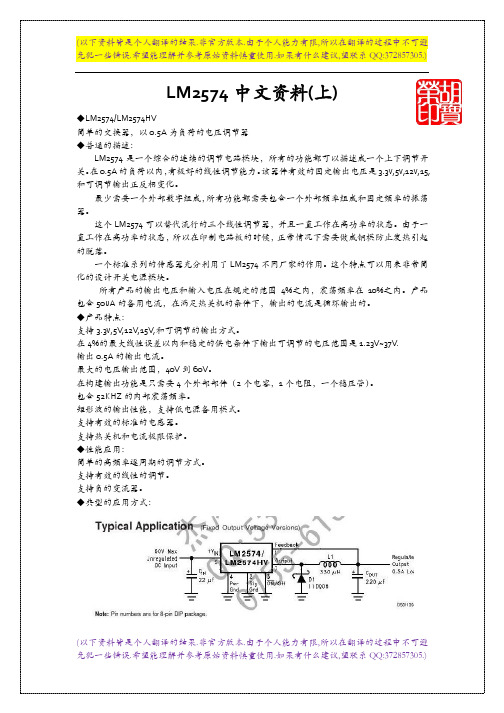
◆典型的应用方式:(以下资料皆是个人翻译的结果.非官方版本.由于个人能力有限,所以在翻译的过程中不可避 免犯一些错误.希望能理解并参考原始资料慎重使用.如果有什么建议,望联系 QQ:372857305.)(以下资料皆是个人翻译的结果.非官方版本.由于个人能力有限,所以在翻译的过程中不可避 免犯一些错误.希望能理解并参考原始资料慎重使用.如果有什么建议,望联系 QQ:372857305.)60V 未校准的 DC 输入◆连接图解:校准的 0.5A 输出◆极限参数: 如果用在军队或者航天上面,则必须用详细的(更好的)设备。
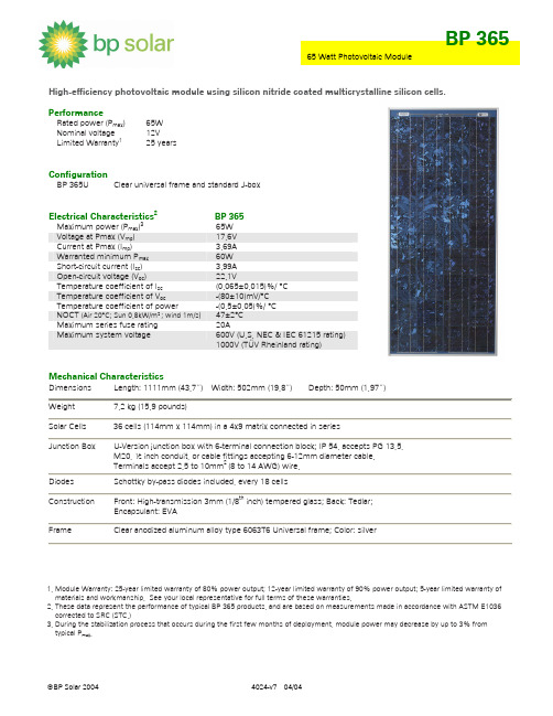
BP365资料
BP 365 I-V Curves
4.5 4.0 3.5 Current (A) 3.0 2.5 2.0 1.5 1.0 0.5 0.0 0 10 20 30 Voltage (V)
t=0C t=25C t=50C t=75C
Listed by Underwriter’s Laboratories for electrical and fire safety (Class C fire rating) Approved by Factory Mutual Research in NEC Class 1, Division 2, Groups C & D hazardous locations (U)
元器件交易网
BP 365
65 Watt Photovoltaic Module
High-efficiency photovoltaic module using silicon nitride coated multicrystalline silicon cells. Performance
Diodes Construction Frame
1. Module Warranty: 25-year limited warranty of 80% power output; 12-year limited warranty of 90% power output; 5-year limited warranty of materials and workmanship. See your local representative for full terms of these warranties. 2. These data represent the performance of typical BP 365 products, and are based on measurements made in accordance with ASTM E1036 corrected to SRC (STC.) 3. During the stabilization process that occurs during the first few months of deployment, module power may decrease by up to 3% from typical Pmax.
hx711官方资料(海芯)
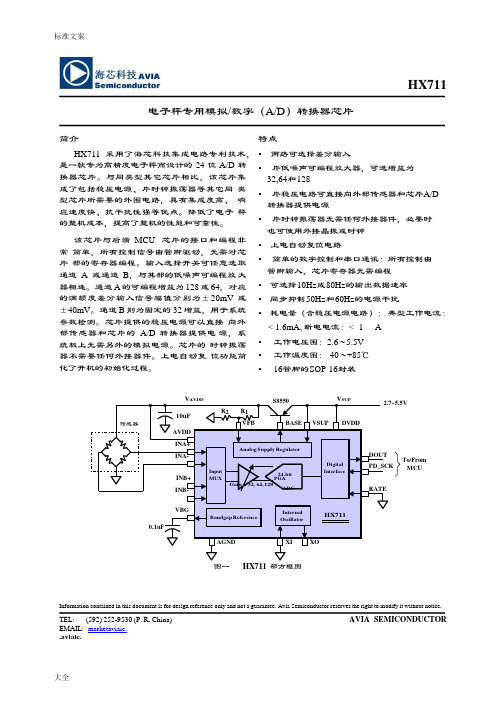
标准文案大全DigitalInterfaceAnalog Supply RegulatorInputMUXInternalOscillatorBandgap ReferenceHX711电子秤专用模拟/数字(A/D)转换器芯片简介HX711 采用了海芯科技集成电路专利技术,是一款专为高精度电子秤而设计的 24 位 A/D 转换器芯片。
与同类型其它芯片相比,该芯片集成了包括稳压电源、片时钟振荡器等其它同类型芯片所需要的外围电路,具有集成度高、响应速度快、抗干扰性强等优点。
降低了电子秤的整机成本,提高了整机的性能和可靠性。
该芯片与后端MCU 芯片的接口和编程非常简单,所有控制信号由管脚驱动,无需对芯片部的寄存器编程。
输入选择开关可任意选取通道A 或通道B,与其部的低噪声可编程放大器相连。
通道 A 的可编程增益为 128 或 64,对应的满额度差分输入信号幅值分别为±20mV 或±40mV。
通道 B 则为固定的 32 增益,用于系统参数检测。
芯片提供的稳压电源可以直接向外部传感器和芯片的A/D 转换器提供电源,系统板上无需另外的模拟电源。
芯片的时钟振荡器不需要任何外接器件。
上电自动复位功能简化了开机的初始化过程。
特点•两路可选择差分输入•片低噪声可编程放大器,可选增益为32,64 和128•片稳压电路可直接向外部传感器和芯片A/D 转换器提供电源•片时钟振荡器无需任何外接器件,必要时也可使用外接晶振或时钟•上电自动复位电路•简单的数字控制和串口通讯:所有控制由管脚输入,芯片寄存器无需编程•可选择10Hz 或80Hz 的输出数据速率•同步抑制50Hz 和60Hz 的电源干扰•耗电量(含稳压电源电路):典型工作电流:< 1.6mA, 断电电流:< 1 A•工作电压围:2.6 ~ 5.5V•工作温度围:-40 ~ +85℃•16 管脚的S OP-16 封装V AVDD10uF R2 R1S8550V SUP 2.7~5.5V传感器AVDDINA+INA-INB+INB-VFBPGAGain = 32, 64, 128BASE VSUP DVDD24-bitADCDOUTPD_SCKRATETo/FromMCU0.1uF VBGHX711 AGND XI XO图一HX711 部方框图Information contained in this document is for design reference only and not a guarantee. Avia Semiconductor reserves the right to modify it without notice. TEL: (592) 252-9530 (P. R. China) AVIA SEMICONDUCTOR EMAIL: marketaviaic..aviaic.大全管脚说明稳压电路电源 VSUP DVDD 数字电源稳压电路控制输出BASE RATE 输出数据速率控制输入 模拟电源 AVDDXI 外部时钟或晶振输入 稳压电路控制输入VFB XO 晶振输入 模拟地 AGND DOUT 串口数据输出参考电源输出 VBG PD_SCK 断电和串口时钟输入通道A 负输入端 INNA INPB 通道B 正输入端 通道A 正输入端INPAINNB通道B 负输入端SOP-16L 封装表一 管脚描述主要电气参数AA(1)有效位数E NBs(Effective Number of Bits) = ln(FSR/RMS Noise)/ln(2)。
LMH6560中文资料
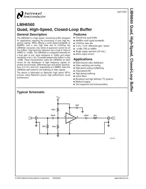
LMH6560Quad,High-Speed,Closed-Loop BufferGeneral DescriptionThe LMH6560is a high speed,closed-loop buffer designed for applications requiring the processing of very high fre-quency signals.While offering a small signal bandwidth of 680MHz,and a very high slew rate of 3100V/µs the LMH6560consumes only 46mA of quiescent current for all four buffers.Total harmonic distortion into a load of 100Ωat 20MHz is −51dBc.The LMH6560is configured internally for a loop gain of one.Input resistance is 100k Ωand output resistance is but 1.5Ω.Crosstalk between the buffers is only −55dB.These characteristics make the LMH6560an ideal choice for the distribution of high frequency signals on printed circuit boards.Differential gain and phase specifica-tions of 0.10%and 0.03˚respectively at 3.58MHz make the LMH6560well suited for the buffering of video signals.The device is fabricated on National’s high speed VIP10process using National’s proven high performance circuit architectures.Featuresn Closed-loop quad buffern 680MHz small signal bandwidth n 3100V/µs slew raten 0.10%/0.03˚differential gain /phase n −51dBc THD at 20MHzn Single supply operation (3V min.)n80mA output currentApplicationsn Multi-channel video distribution n Video switching and routing n High-speed analog multiplexing n Channelized EWn High-density buffering n Active filtersn Broadcast and high definition TV systems n Medical imagingnTest equipment and instrumentationTypical Schematic20064235April 2003LMH6560Quad,High-Speed,Closed-Loop Buffer©2003National Semiconductor Corporation Absolute Maximum Ratings(Note 1)If Military/Aerospace specified devices are required,please contact the National Semiconductor Sales Office/Distributors for availability and specifications.ESD Tolerance Human Body Model 2000V (Note 2)Machine Model200V (Note 3)Output Short Circuit Duration (Note 4),(Note 5)Supply Voltage (V +–V −)13VVoltage at Input/Output Pins V ++0.8V,V −−0.8VSoldering InformationInfrared or Convection (20sec.)235˚CWave Soldering (10sec.)260˚CStorage Temperature Range −65˚C to +150˚CJunction Temperature (Note 6)+150˚COperating Ratings (Note 1)Supply Voltage (V +–V −)3-10VOperating Temperature Range (Note 6),(Note 7)−40˚C to +85˚CPackage Thermal Resistance (Note 6),(Note 7)14-Pin SOIC 137˚C/W 14-Pin TSSOP160˚C/W±5V Electrical CharacteristicsUnless otherwise specified,all limits guaranteed for T J =25˚C,V +=+5V,V −=−5V,V O =V CM =0V and R L =100Ωto 0V.Boldface limits apply at the temperature extremes.Symbol ParameterConditionsMin (Note 9)Typ (Note 8)Max (Note 9)Units Frequency Domain ResponseSSBW Small Signal Bandwidth V O <0.5V PP 680MHz GFN Gain Flatness <0.1dB V O <0.5V PP375MHz FPBW Full Power Bandwidth (−3dB)V O =2V PP (+10dBm)280MHZ DG Differential Gain R L =150Ωto 0V;f =3.58MHz 0.10%DPDifferential PhaseR L =150Ωto 0V;f =3.58MHz 0.03degTime Domain Response t r Rise Time 3.3V Step (20-80%)0.6ns t f Fall Time0.7ns t s Settling Time to 0.1% 3.3V Step 9ns OS Overshoot 1V Step 4%SR Slew Rate(Note 11)3100V/µs Distortion And Noise PerformanceHD22nd Harmonic Distortion V O =2V PP ;f =20MHz −58dBc HD33rdHarmonic DistortionV O =2V PP ;f =20MHz −52dBc THD Total Harmonic Distortion V O =2V PP ;f =20MHz −51dBc e n Input-Referred Voltage Noise f =1MHz 3nV/CP 1dB Compression Point f =10MHz+23dBm CT Amplifier Crosstalk Receiving Amplifier:R S =50Ωto 0V;f =10MHz −55dB SNR Signal to Noise Ratio f =5MHz;V O =1V PP 120dB AGMAmplifier Gain MatchingR L =2k Ωto 0V;f =5MHz;V O =1V PP0.05dBStatic,DC Performance A CLSmall Signal Voltage GainV O =100mV PP R L =100Ωto 0V 0.970.995V/VV O =100mV PP R L =2k Ωto 0V0.990.998V OS Input Offset Voltage22025mV TC V OSTemperature Coefficient Input Offset Voltage(Note 12)28µV/˚CL M H 6560 2±5V Electrical Characteristics(Continued)Unless otherwise specified,all limits guaranteed for T J=25˚C,V+=+5V,V−=−5V,V O=V CM=0V and R L=100Ωto0V. Boldface limits apply at the temperature extremes.Symbol Parameter ConditionsMin(Note9)Typ(Note8)Max(Note9)UnitsI B Input Bias Current(Note10)−10−14−5µATC I B Temperature Coefficient InputBias Current(Note12)−4.7nA/˚CR OUT Output Resistance R L=100Ωto0V;f=100kHz 1.5ΩR L=100Ωto0V;f=10MHz 1.6PSRR Power Supply Rejection Ratio V S=±5V to V S=±5.25V;V IN=0V 484467dBI S Supply Current,All4Buffers No Load465863mA Miscellaneous PerformanceR IN Input Resistance100kΩC IN Input Capacitance2pFV O Output Swing Positive R L=100Ωto0V 3.103.083.34VR L=2kΩto0V 3.583.553.64Output Swing Negative R L=100Ωto0V−3.34−3.20−3.17VR L=2kΩto0V−3.64−3.58−3.55I SC Output Short Circuit Current Sourcing:V IN=V+;V O=0V−83mASinking:V IN=V−;V O=0V83I O Linear Output Current Sourcing:V IN-V O=0.5V(Note10)−50−42−74mASinking:V IN-V O=−0.5V (Note10)5040745V Electrical CharacteristicsUnless otherwise specified,all limits guaranteed for T J=25˚C,V+=+5V,V−=0V,V O=V CM=V+/2and R L=100Ωto V+/2. Boldface limits apply at the temperature extremes.Symbol Parameter ConditionsMin(Note9)Typ(Note8)Max(Note9)UnitsFrequency Domain ResponseSSBW Small Signal Bandwidth V O<0.5V PP455MHzGFN Gain Flatness<0.1dB V O<0.5V PP75MHzFPBW Full Power Bandwidth(−3dB)V O=2V PP(+10dBm)175MHZDG Differential Gain R L=150Ωto V+/2;f=3.58MHz0.4%DP Differential Phase R L=150Ωto V+/2;f=3.58MHz0.09degTime Domain Responset r Rise Time 2.3V PP Step(20-80%)0.8nst f Fall Time 1.0nst s Settling Time to0.1% 2.3V Step10nsOS Overshoot1V Step0%SR Slew Rate(Note11)1445V/µsLMH656035V Electrical Characteristics(Continued)Unless otherwise specified,all limits guaranteed for T J =25˚C,V +=+5V,V −=0V,V O =V CM =V +/2and R L =100Ωto V +/2.Boldface limits apply at the temperature extremes.Symbol ParameterConditionsMin (Note 9)Typ (Note 8)Max (Note 9)Units Distortion And Noise PerformanceHD22nd Harmonic Distortion V O =2V PP ;f =20MHz −52dBc HD33rd Harmonic Distortion V O =2V PP ;f =20MHz −54dBc THD Total Harmonic Distortion V O =2V PP ;f =20MHz −50dBc e n Input-Referred Voltage Noise f =1MHz 3nV/CP 1dB Compression Point f =10MHz+14dBm CT Amplifier Crosstalk Receiving Amplifier:R S =50Ωto V +/2;f =10MHz −55dB SNR Signal to Noise Ratio V O =1V PP ;f =5MHz 120dB AGMAmplifier Gain MatchingV O =1V PPR L =2k Ωto V +/2;f =5MHz 0.5dBStatic,DC Performance A CLSmall Signal Voltage GainV O =100mV PPR L =100Ωto V +/20.970.994V/VV O =100mV PP R L =2k Ωto V +/20.990.998V OS Input Offset Voltage21315mV TC V OS Temperature Coefficient Input Offset Voltage (Note 12)2µV/˚C I B Input Bias Current(Note 10)−5−5.5−2.5µA TC I B Temperature Coefficient Input Bias Current (Note 12)1.3nA/˚CR OUTOutput ResistanceR L =100Ωto V +/2;f =100kHz 1.7ΩR L =100Ωto V +/2;f =10MHz2.0PSRR Power Supply Rejection Ratio V S =+5V to V S =+5.5V;V IN =V S /2484567dB I SSupply Current All 4BufferNo Load212630mAMiscellaneous Performance R IN Input Resistance 16k ΩC IN Input Capacitance 2pFV OOutput Swing PositiveR L =100Ωto V +/2 3.743.70 3.85V R L =2k Ωto V +/23.923.903.96Output Swing NegativeR L =100Ωto V +/2 1.15 1.221.27VR L =2k Ωto V +/21.04 1.081.10I SC Output Short Circuit Current Sourcing:V IN =V +;V O =V +/2−40mASinking:V IN =V −;V O =V +/222I OLinear Output CurrentSourcing:V IN -V O =0.5V (Note 10)−50−40−64mASinking:V IN -V O =−0.5V (Note 10)302045L M H 6560 43V Electrical CharacteristicsUnless otherwise specified,all limits guaranteed for T J =25˚C,V +=3V,V −=0V,V O =V CM =V +/2and R L =100Ωto V +/2.Boldface limits apply at the temperature extremes.Symbol ParameterConditionsMin (Note 9)Typ (Note 8)Max (Note 9)Units Frequency Domain ResponseSSBW Small Signal Bandwidth V O <0.5V PP 265MHz GFN Gain Flatness <0.1dB V O <0.5V PP40MHz FPBW Full Power Bandwidth (−3dB)V O =1V PP (+4.5dBm)115MHZ Time Domain Responset r Rise Time 1V Step (20-80%) 1.1ns t f Fall Time1.3ns t s Settling Time to 0.1%1V Step 11ns OS Overshoot 0.5V Step 0%SR Slew Rate(Note 11)480V/µs Distortion And Noise PerformanceHD22nd Harmonic Distortion V O =0.5V PP ;f =20MHz −55dBc HD33rdHarmonic DistortionV O =0.5V PP ;f =20MHz −61dBc THD Total Harmonic Distortion V O =0.5V PP ;f =20MHz −54dBc e n Input-Referred Voltage Noise f =1MHz 3nV/CP 1dB Compression Point f =10MHz+4dBm CT Amplifier Crosstalk Receiving Amplifier:R S =50Ωto V +/2;f =10MHz −55dB SNR Signal to Noise Ratio f =5MHz;V O =1V PP 120dB AGMAmplifier Gain MatchingR L =2k Ωto V +/2;f =5MHz;V O =1V PP 0.4dBStatic,DC Performance A CLSmall Signal Voltage GainV O =100mV PPR L =100Ωto V +/20.970.99V/VV O =100mV PP R L =2k Ωto V +/20.990.997V OS Input Offset Voltage1.6810mV TC V OS Temperature Coefficient Input Offset Voltage (Note 12) 2.6µV/˚C I B Input Bias Current(Note 10)−3−3.5−1.4µA TC I B Temperature Coefficient Input Bias Current (Note 12)0.3nA/˚CR OUTOutput ResistanceR L =100Ωto V +/2;f =100kHz 2.1ΩR L =100Ωto V +/2;f =10MHz2.8PSRR Power Supply Rejection Ratio V S =+3V to V S =+3.5V;V IN =V S /2484665dB I SSupply Current,All 4BuffersNo Load111518mAMiscellaneous Performance R IN Input Resistance 17k ΩC INInput Capacitance2pFLMH656053V Electrical Characteristics(Continued)Unless otherwise specified,all limits guaranteed for T J =25˚C,V +=3V,V −=0V,V O =V CM =V +/2and R L =100Ωto V +/2.Boldface limits apply at the temperature extremes.Symbol ParameterConditionsMin (Note 9)Typ (Note 8)Max (Note 9)UnitsV OOutput Swing PositiveR L =100Ωto V +/2 2.01.93 2.05VR L =2k Ωto V +/22.12.02.15Output Swing NegativeR L =100Ωto V +/20.95 1.01.07VR L =2k Ωto V +/20.850.901.0I SC Output Short Circuit Current Sourcing:V IN =V +;V O =V +/2−26mASinking:V IN =V −;V O =V +/214I OLinear Output CurrentSourcing:V IN -V O =0.5V (Note 10)−20−13−30mASinking:V IN -V O =−0.5V (Note 10)12820Note 1:Absolute Maximum Ratings indicate limits beyond which damage to the device may occur.Operating Ratings indicate conditions for which the device is intended to be functional,but specific performance is not guaranteed.For guaranteed specifications and the test conditions,see the Electrical Characteristics.Note 2:Human body model,1.5k Ωin series with 100pF Note 3:Machine Model,0Ωin series with 200pF.Note 4:Applies to both single-supply and split-supply operation.Continuous short circuit operation at elevated ambient temperature can result in exceeding the maximum allowed junction temperature of 150˚C.Note 5:Short circuit test is a momentary test.See next note.Note 6:The maximum power dissipation is a function of T J(MAX),θJA ,and T A .The maximum allowable power dissipation at any ambient temperature is P D =(T J(MAX)-T A )/θJA .All numbers apply for packages soldered directly onto a PC board.Note 7:Electrical Table values apply only for factory testing conditions at the temperature indicated.Factory testing conditions result in very limited self-heating of the device such that T J =T A .There is no guarantee of parametric performance as indicated in the electrical tables under conditions of internal self-heating where T J >T A .See Applications section for information on temperature de-rating of this device.Note 8:Typical Values represent the most likely parametric norm.Note 9:All limits are guaranteed by testing or statistical analysis.Note 10:Positive current corresponds to current flowing into the device.Note 11:Slew rate is the average of the positive and negative slew rate.Average Temperature Coefficient is determined by dividing the change in a parameter at temperature extremes by the total temperature change.Note 12:Average Temperature Coefficient is determined by dividing the change in a parameter at temperature extremes by the total temperature change.L M H 6560 6LMH6560 Connection Diagram14-Pin SOIC/TSSOP Array20064234Top ViewOrdering InformationPackage Part Number Package Marking Transport Media NSC Drawing14-pin SOIC LMH6560MA LMH6560MA55Units/Rail M14ALMH6560MAX 2.5k Units Tape and Reel14-pin TSSOP LMH6560MT LMH6560MT94Units/Rail MTC14LMH6560MTX 2.5k Units Tape and Reel7Typical Performance CharacteristicsAt T J =25˚C,V +=+5V,V −=−5V;unless otherwise speci-fied.Frequency ResponseFrequency Response Over Temperature2006420620064207Gain Flatness 0.1dB Differential Gain and Phase2006420820064204Differential Gain and Phase Transient Response Positive2006420520064228L M H 6560 8Typical Performance Characteristics At T J =25˚C,V +=+5V,V −=−5V;unless otherwisespecified.(Continued)Transient Response NegativeTransient Response Positive for Various V SUPPLY2006422620064227Transient Response Negative for Various V SUPPLY Harmonic Distortion vs.V OUT @5MHz2006422520064211Harmonic Distortion vs.V OUT @10MHz Harmonic Distortion vs.V OUT @20MHz2006420920064210LMH65609Typical Performance Characteristics At T J =25˚C,V +=+5V,V −=−5V;unless otherwisespecified.(Continued)THD vs.V OUT for Various FrequenciesVoltage Noise2006422420064229Linearity V OUT vs.V INCrosstalk vs.Frequency2006422020064202Crosstalk vs.TimeV OS vs.V SUPPLY for 3Units2006420320064230L M H 6560 10Typical Performance Characteristics At TJ=25˚C,V+=+5V,V−=−5V;unless otherwise specified.(Continued)V OS vs.V SUPPLY for Unit1V OS vs.V SUPPLY for Unit22006423120064232 V OS vs.V SUPPLY for Unit3I B vs.V SUPPLY(Note10)2006423320064212 R OUT vs.Frequency PSRR vs.Frequency2006422120064222LMH6560Typical Performance Characteristics At T J =25˚C,V +=+5V,V −=−5V;unless otherwisespecified.(Continued)I SUPPLY vs.V SUPPLYI SUPPLY vs.V IN2006421620064236V OUT vs.I OUT (Sinking)V OUT vs.I OUT (Sourcing)2006421520064201I OUT Sinking vs.V SUPPLY I OUT Sourcing vs.V SUPPLY2006421320064214L M H 6560Typical Performance Characteristics At TJ=25˚C,V+=+5V,V−=−5V;unless otherwise specified.(Continued)Small Signal Pulse Response Large Signal Pulse Response@V S=3V2006422320064219 Large Signal Pulse Response@V S=5V Large Signal Pulse Response@V S=10V2006421820064217LMH6560Application NotesUSING BUFFERSA buffer is an electronic device delivering current gain but no voltage gain.It is used in cases where low impedances need to be driven and more drive current is required.Buffers need a flat frequency response and small propagation delay.Fur-thermore,the buffer needs to be stable under resistive,capacitive and inductive loads.High frequency buffer appli-cations require that the buffer be able to drive transmission lines and cables directly.IN WHAT SITUATION WILL WE USE A BUFFER?In case of a signal source not having a low output impedance one can increase the output drive capability by using a buffer.For example,an oscillator might stop working or have frequency shift which is unacceptably high when loaded heavily.A buffer should be used in that situation.Also in the case of feeding a signal to an A/D converter it is recom-mended that the signal source be isolated from the A/D ing a buffer assures a low output impedance,the delivery of a stable signal to the converter,and accom-modation of the complex and varying capacitive loads that the A/D converter presents to the Op Amp.Optimum value is often found by experimentation for the particular application.The use of buffers is strongly recommended for the handling of high frequency signals,for the distribution of signals through transmission lines or on pcb’s,or for the driving of external equipment.There are several driving options:•Use one buffer to drive one transmission line (see Figure 1)•Use one buffer to drive to multiple points on one trans-mission line (see Figure 2)•Use one buffer to drive several transmission lines each driving a different receiver.(see Figure 3)In these three options it is seen that there is more than one preferred method to reach an (end)point on a transmission line.Until a certain point the designer can make his own choice but the designer should keep in mind never to break the rules about high frequency transport of signals.An ex-planation follows in the text below.TRANSMISSION LINESIntroduction to transmission lines .The following is an over-view of transmission line theory.Transmission lines can be used to send signals from DC to very high frequencies.At all points across the transmission line,Ohm’s law must apply.For very high frequencies,parasitic behavior of the PCB or cable comes into play.The type of cable used must match the application.For example an audio cable looks like a coax cable but is unusable for radar frequencies at 10GHz.In this case one have to use special coax cables with lower attenu-ation and radiation characteristics.Normally a pcb trace is used to connect components on a pcb board together.An important consideration is the amount of current carried by these pcb traces.Wider pcb traces are required for higher current densities and for ap-plications where very low series resistance is needed.When routed over a ground plane,pcb traces have a defined characteristic impedance.In many design situations charac-teristic impedance is not utilized.In the case of high fre-quency transmission,however it is necessary to match the load impedance to the line characteristic impedance (more on this later).Each trace is associated with a certain amount of series resistance and series inductance and also exhibits parallel capacitance to the ground plane.The combination of these parameters defines the line’s characteristic imped-ance.The formula with which we calculate this impedance is as follows:Z 0=√(L/C)In this formula L and C are the value/unit length,and R is assumed to be zero.C and L are unknown in many cases so we have to follow other steps to calculate the Z 0.The char-acteristic impedance is a function of the geometry of the cross section of the line.In (Figure 4)we see three cross sections of commonly used transmission lines.20064237FIGURE 1.20064238FIGURE 2.20064239FIGURE 3.L M H 6560Application Notes(Continued)Z 0can be calculated by knowing some of the physical di-mensions of the pcb line,such as pcb thickness,width of the trace and e r ,relative dielectric constant.The formula given in transmission line theory for calculating Z 0is as follows:(1)e r relative dielectric constant h pcb height W trace widthth thickness of the copperIf we ignore the thickness of the copper in comparison to the width of the trace then we have the following equation:(2)With this formula it is possible to calculate the line imped-ance vs.the trace width.Figure 5shows the impedance associated with a given line ing the same formula it is also possible to calculate what happens when e r varies over a certain range of values.Varying the e r over a range of 1to 10gives a variation for the Characteristic Impedance of about 40Ωfrom 80Ωto 38Ω.Most transmission lines are designed to have 50Ωor 75Ωimpedance.The reason for that is that in many cases the pcb trace has to connect to a cable whose impedance is either 50Ωor 75Ω.As shown e r and the line width influence this value.Next,there will be a discussion of some issues associated with the interaction of the transmission line at the source and at the load.Connecting a Load Using a Transmission LineIn most cases,it is unrealistic to think that we can place a driver or buffer so close to the load that we don’t need a transmission line to transport the signal.The pcb trace length between a driver and the load may affect operation depending upon the operating frequency.Sometimes it is possible to do measurements by connecting the DUT directly to the analyzer.As frequencies become higher the short lines from the DUT to the analyzer become long lines.When this happens there is a need to use transmission lines.The next point to examine is what happens when the load is connected to the transmission line.When driving a load,it is important to match the line and load impedance,otherwise reflections will occur and this phenomena will distort the signal.If a transient is applied at T =0(Figure 6,trace A)the resultant waveform may be observed at the start point of the transmission line.At this point (begin)on the transmission line the voltage increases to (V)and the wave front travels along the transmission line and arrives at the load at T =10.At any point across along the line I =V/Z 0,where Z 0is the impedance of the transmission line.For an applied transient of 2V with Z 0=50Ωthe current from the buffer output stage is 40mA.Many vintage op amps cannot deliver this level of current because of an output current limitation of about 20mA or even less.At T =10the wave front arrives at the load.Since the load is perfectly matched to the transmission line all of the current traveling across the line will be ab-sorbed and there will be no reflections.In this case source and load voltages are exactly the same.When the load and the transmission line have unequal values of impedance a different situation results.Remember there is another basic which says that energy cannot be lost.The power in the transmission line is P =V 2/R.In our example the total power is 22/50=80mW.Assume a load of 75Ω.In that case a power of 80mW arrives at the 75Ωload and causes a voltage of the proper amplitude to maintain the incoming power.20064240FIGURE 4.20064243FIGURE 5.LMH6560Application Notes(Continued)(3)The voltage wavefront of 2.45V will now set about traveling back over the transmission line towards the source,thereby resulting in a reflection caused by the mismatch.On the other hand if the load is less then 50Ωthe backwards traveling wavefront is subtracted from the incoming voltage of 2V.Assume the load is 40Ω.Then the voltage across the load is:(4)This voltage is now traveling backwards through the line toward the start point.In the case of a sinewave interfer-ences develop between the incoming waveform and the backwards-going reflections,thus distorting the signal.If there is no load at all at the end point the complete transient of 2V is reflected and travels backwards to the beginning of the line.In this case the current at the endpoint is zero and the maximum voltage is reflected.In the case of a short at the end of the line the current is at maximum and the voltage is zero.Using Serial and Parallel TerminationMany applications,such as video,use a series resistance between the driver and the transmission line (see Figure 1).In this case the transmission line is terminated with the characteristic impedance at both ends of the line.See Figure 6trace B.The voltage traveling through the transmission lineis half the voltage seen at the output of the buffer,because the series resistor in combination with Z 0forms a two-to-on voltage divider.The result is a loss of 6dB.For video appli-cations,amplifier gain is set to 2in order to realize an overall gain of 1.Many operational amplifiers have a relatively flat frequency response when set to a gain of two compared to unity gain.In trace B it is seen that,if the voltage reaches the end of the transmission line,the line is perfectly matched and no reflections will occur.The end point voltage stays at half the output voltage of the opamp or buffer.Driving More Than One InputAnother transmission line possibility is to route the trace via several points along a transmission line (see Figure 2).This is only possible if care is taken to observe certain restric-tions.Failure to do so will result in impedance discontinuities that will cause distortion of the signal.In the configuration of Figure 2there is a transmission line connected to the buffer output and the end of the line is terminated with Z 0.We have seen in the section ’Connecting a load using a transmission line’that for the condition above,the signal throughout the entire transmission line has the same value,that the value is the nominal value initiated by the opamp output,and no reflections occur at the end point.Because of the lack of reflections no interferences will occur.Consequently the sig-nal has every where on the line the same amplitude.This allows the possibility of feeding this signal to the input port of any device which has high ohmic impedance and low input capacitance.In doing so keep in mind that the transient arrives at different times at the connected points in the transmission line.The speed of light in vacuum,which is about 3*108m/sec,reduces through a transmission line or a cable down to a value of about 2*108m/sec.The distance the signal will travel in 1ns is calculated by solving the following formula:S =V*tWhereS =distanceV =speed in the cableT =timeThis calculation gives the following result:s =2*108*1*10-9=0.2mThat is for each nanosecond the wave front shifts 20cm over the length of the transmission line.Keep in mind that in a distance of just 2cm the time displacement is already ing Serial Termination To More Than One Transmission LineAnother way to reach several points via a transmission line is to start several lines from one buffer output (see Figure 3).This is possible only if the output can deliver the needed current into the sum of all transmission lines.As can be seen in this figure there is a series termination used at the begin-ning of the transmission line and the end of the line has no termination.This means that only the signal at the endpoint is usable because at all other points the reflected signal will cause distortion over the line.Only at the endpoint will the measured signal be the same as at the startpoint.Referring to Figure 6trace C,the signal at the beginning of the line has a value of V/2and at T =0this voltage starts traveling towards the end of the transmission line.Once at the end-point the line has no termination and 100%reflection will occur.At T =10the reflection causes the signal to jump to 2V and to start traveling back along the line to the buffer (see Figure 6trace D).Once the wavefront reaches the series20064246FIGURE 6.L M H 6560Application Notes(Continued)termination resistor,provided the termination value is Z0,thewavefront undergoes total absorption by the termination.This is only true if the output impedance of the buffer/driveris low in comparison to the characteristic impedance Z0.Atthis moment the voltage in the whole transmission line hasthe nominal value of2V(see Figure6trace E).If the threetransmission lines each have a different length the particularpoint in time at which the voltage at the series terminationresistor jumps to2V is different for each case.However,thistransient is not transferred to the other lines because theoutput of the buffer is low and this transient is highly attenu-ated by the combination of the termination resistor and theoutput impedance of the buffer.A simple calculation illus-trates the point.Assume that the output impedance is5Ω.For the frequency of interest the attenuation is V B/V A=55/5=11,where A and B are the points in Figure3.In this casethe voltage caused by the reflection is2/11=0.18V.Thisvoltage is transferred to the remaining transmission lines insequence and following the same rules as before this volt-age is seen at the end points of those lines.The lower theoutput resistance the higher the decoupling between thedifferent lines.Furthermore one can see that at the endpointof these transmission lines there is a normal transient equalto the original transient at the beginning point.However at allother points of the transmission line there is a step voltage atdifferent distances from the startpoint depending at whatpoint this is measured(see trace D).Measuring the Length of a Transmission LineAn open transmission line can be used to measure thelength of a particular transmission line.As can be seen inFigure7.The line of interest has a certain length.A transientis applied at T=0and at that point in time the wavefrontstarts traveling with an amplitude of V/2towards the end ofthe line where it is reflected back to the startpoint.To calculate the length of the line it is necessary to measureimmediately after the series termination resistor.The voltageat that point remains at half nominal voltage,thus V/2,untilthe reflection returns and the voltage jumps to V.During aninterval of5ns the signal travels to the end of the line wherethe wave front is reflected and returns to the measurementpoint.During the time interval when the wavefront is travel-ing to the end of the transmission line and back the voltagehas a value of V/2.This interval is10ns.The length can becalculated with the following formula:S=(V*T)/2(5)As calculated before in the section‘Driving more than oneinput’the signal travels20cm/ns so in5ns this distanceindicated distance is1m.So this example is easily verified.APPLYING A CAPACITIVE LOADThe assumption of pure resistance for the purpose of con-necting the output stage of a buffer or opamp to a load isappropriate as a first approximation.Unfortunately that isonly a part of the truth.Associated with this resistor is acapacitor in parallel and an inductor in series.Any capaci-tance such as C1-1which is connected directly to the outputstage is active in the loop gain as see in Figure8.Outputcapacitance,present also at the minus input in the case of abuffer,causes an increasing phase shift leading to instabilityor even oscillation in the circuit.Unfortunately the leads of the output capacitor also containseries inductors which become more and more important athigh frequencies.At a certain frequency this series capacitorand inductor forms an LC combination which becomes se-ries resonant.At the resonant frequency the reactive com-ponent vanishes leaving only the ohmic resistance(R-1orR-2)of the series L/C combination.(see Figure9).Consider a frequency sweep over the entire spectrum forwhich the LMH6559high frequency buffer is active.In thefirst instance peaking occurs due to the parasitic capaci-tance connected at the load whereas at higher frequenciesthe effects of the series combination of L and C become20064247FIGURE7.20064249FIGURE8.20064250FIGURE9.LMH6560。
MTD658中文资料
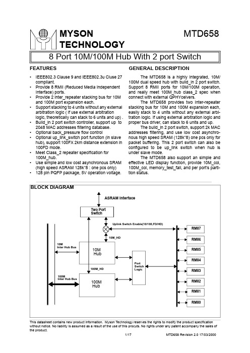
TECHNOLOGYFEATURESGENERAL DESCRIPTIONBLOCK DIAGRAM•IEEE802.3 Clause 9 and IEEE802.3u Cluse 27 compliant.•Provide 8 RMII (Reduced Media Independent Interface) ports.•Provide 2 inter_repeater stacking bus for 10M and 100M port expansion each.•Support stacking to 4 units without any external arbitration logic ( if use external arbitration logic, theoretically can stack to 6 units and up) .•Build_in 2 port switch controller, support up to 2048 MAC addresses filtering database.•Optional back_pressure flow control•Optional up_link_switch port function (in slave hub), support 100FX 2km distance extension in 100FD mode.•Meet Class_2 repeater specification for 100M_hub.•Use simple and low cost asynchronous SRAM (high speed ASRAM 128k*8 : one pcs only) •128 pin PQFP package, 5V operation voltage.8 Port 10M/100M Hub With 2 port SwitchThe MTD658 is a highly integrated, 10M/100M dual speed hub with build_in 2 port switch.Support 8 RMII ports for 10M/100M operation,and really meet 100M_hub class_2 spec when connect with external QPHYceivers.The MTD658 provides two Inter-repeater stacking bus for 10M and 100M expansion each,easily stack to 4 units without any external arbi-tration logic. If using external arbitration logic and proper bus driver, can stack to 6 units and up.The build_in 2 port switch, support 2k MAC addresses filtering, and use low cost asynchro-nous high speed SRAM (128k*8) one pcs only for packet buffering. This 2 port switch can also be configured to be up_link switch when hub is under slave mode.The MTD658 also support an simple and effective LED display function, provide 10M_col,100M_col, memory_test_fail, and per port’s parti-tion status.ASRAM InterfaceRMII7RMII6RMII5RMII4RMII3RMII2RMII1RMII010M Hub100M HubTwo PortSwitchUplink Switch Enable(10/100,FD/HD)10M_HD100M_HDPort Switch Logic10MInter Hub Bus100MInter Hub BusTECHNOLOGY SYSTEM DIAGRAMMTD658MTD658QUAD PHYsceiverQUAD PHYsceiverASRAM (128kx8)10MInter Hub Bus100MInter Hub Bus10MInter Hub Bus100MInter Hub Bus MTD658MTD65810MInter Hub Bus100MInter Hub Bus10MInter Hub Bus100MInter Hub BusRMII0-3RMII4-7DB25 ConnectorQUAD TransformerQUAD TransformerRJ45RJ45TECHNOLOGY1.0 PIN CONNECTION1021011009998979695949392919089888786858483828180797877767574737271706968676665103104105106107108109110111112113114115116117118119120121122123124125126127128A 11A 5A 9A 6A 8A 7A 13A 12W EB A 14G N D A 15A 16I R E Q 10_O U T I R E Q 10_I N 0I R E Q 10_I N 1I R E Q 10_I N 2IC O L B 10I A C K B 10I C L K 10G ND I D A T 10I RE Q 100_O U T I R E Q 100_I N 0I R E Q 100_I N 1I R E Q 100_I N 2I C O L B 100I A C K B 100G N D I C L K 100V C C I D A T 100_0I D A T 100_1I D A T 100_2I D A T 100_3I M A S T E RF D 7U P S W E NVCC A4GND OEB A3A10A2A1D7A0D6D0D5D1GND D4D2D3VCC SYSCLK GND LEDDAT LEDCLK MDC MDIO RSTB0102030405060708091011121314151617181920212223242526272829303132333435363738C R SD V 0T X D 0_1V C C T X D 0_0T XE N 0R X D 0_0R X D 0_1C R S D V 1T X D 1_1T X D 1_0T X E N 1R X D 1_0R X D 1_1G N D C R S D V 2T X D 2_1T X D 2_0T X E N 2R X D 2_0R X D 2_1C R S D V 3T X D 3_1T X D 3_0T X E N 3R X D 3_0R X D 3_1S P D 3S P D 2S P D 1S P D 0V C C G N D C R S D V 4T X D 4_1T X D 4_0T X E N 4R X D 4_0R X D 4_1MTD6586463626160595857565554535251504948474645444342414039SPD4SPD5SPD6SPD7GND VCC RXD7_1RXD7_0TXEN7TXD7_0TXD7_1CRSDV7RXD6_1RXD6_0TXEN6TXD6_0TXD6_1CRSDV6GND VCC RXD5_1RXD5_0TXEN5TXD5_0TXD5_1CRSDV5TECHNOLOGY2.0 PIN DESCRIPTIONSRMII Port Interface PinsName Pin Number I/O DescriptionsCRSDV01I Port0 RMII receive interface signal, CRSDV0 is asserted high whenport0 media is non_idle.RXD0_0 RXD0_167IIPort0 RMII receive data bit_0.Port0 RMII receive data bit_1.TXEN05O Port0 RMII transmit enable signal.TXD0_0 TXD0_142OOPort0 RMII transmit data bit_0.Port0 RMII transmit data bit_1.CRSDV18I Port1 RMII receive interface signal, CRSDV1 is asserted high whenport1 media is non_idle.RXD1_0 RXD1_11213IIPort1 RMII receive data bit_0.Port1 RMII receive data bit_1.TXEN111O Port1 RMII transmit enable signal.TXD1_0 TXD1_1109OOPort1 RMII transmit data bit_0.Port1 RMII transmit data bit_1.CRSDV215I Port2 RMII receive interface signal, CRSDV2 is asserted high whenport2 media is non_idle.RXD2_0 RXD2_11920IIPort2 RMII receive data bit_0.Port2 RMII receive data bit_1.TXEN218O Port2 RMII transmit enable signal.TXD2_0 TXD2_11716OOPort2 RMII transmit data bit_0.Port2 RMII transmit data bit_1.CRSDV321I Port3 RMII receive interface signal, CRSDV3 is asserted high whenport3 media is non_idle.RXD3_0 RXD3_12526IIPort3 RMII receive data bit_0.Port3 RMII receive data bit_1.TXEN324O Port3 RMII transmit enable signal.TXD3_0 TXD3_12322OOPort3 RMII transmit data bit_0.Port3 RMII transmit data bit_1.CRSDV433I Port4 MII receive interface signal, CRSDV4 is asserted high whenport4 media is non_idle.RXD4_0 RXD4_13738IIPort4 RMII receive data bit_0.Port4 RMII receive data bit_1.TXEN436O Port4 RMII transmit enable signal.TXD4_0 TXD4_13534OOPort4 RMII transmit data bit_0.Port4 RMII transmit data bit_1.CRSDV539I Port5 RMII receive interface signal, CRSDV5 is asserted high whenport5 media is non_idle.RXD5_0 RXD5_14344IIPort5 RMII receive data bit_0.Port5 RMII receive data bit_1.TXEN542O Port5 RMII transmit enable signal. TXD5_0O Port5 RMII transmit data bit_0.TECHNOLOGYNote: Asynchronous SRAM acess time: 10/12 ns (max)CRSDV647I Port6 RMII receive interface signal, CRSDV6 is asserted high whenport6 media is non_idle.RXD6_0RXD6_15152I I Port6 RMII receive data bit_0.Port6 RMII receive data bit_1.TXEN650O Port6 RMII transmit enable signal.TXD6_0TXD6_14948O O Port6 RMII transmit data bit_0.Port6 RMII transmit data bit_1.CRSDV753I Port7 RMII receive interface signal, CRSDV7 is asserted high when port7 media is non_idle.RXD7_0RXD7_15758I I Port7 RMII receive data bit_0.Port7 RMII receive data bit_1.TXEN756O Port7 RMII transmit enable signal.TXD7_0TXD7_15554O OPort7 RMII transmit data bit_0.Port7 RMII transmit data bit_1.High Speed Asynchronous SRAM Interface PinsName Pin NumberI/O Descriptions WEB 94O ASRAM control pin for write (low active).OEB 106O ASRAM control pin for read (low active).D[7:0]111,113,115,118,120,119,116,114I/O ASRAM data busA[16:0]90,91,93,96,95,102,108,100,98,97,99,101,104,107,109,110,112O ASRAM address busRMII Port Interface PinsName Pin NumberI/O DescriptionsTECHNOLOGY10M Inter-Bus Interface pinsName Pin Number I/O DescriptionsIMASTER67I Master hub selection:when high: means hub internal inter_bus arbiter is enabled and hub internal two_port switch is well conneted to 10M_hub core and100M_hub core .when low: means hub internal inter_bus arbiter is disabled and hub internal two_port switch is not connected to 10M_hub core and100M_hub core.IACKB1084I/O10M Inter-Bus port access acknowledge signal (low active). For master hub, this pin is output; for slave hub is input, or while EXT_ARBjumper was set to “1”, this pin is input from an external arbitrationdevice.ICOLB1085I/O10M Inter-Bus collision signal (low active). For master hub, this pin can output multi hub collision event to inform all slave hub ; for slave hub, this pin is an input, or while EXT_ARB jumper was set to “1”, this pin is input from an external arbitration device.IREQ10_IN088I10M Inter-Bus port access request input. IREQ10_IN187I10M Inter-Bus port access request input. IREQ10_IN286I10M Inter-Bus port access request input. IREQ10_OUT89O10M Inter-Bus port access request output. ICLK1083I/O10M Inter-Bus port clock.IDAT1081I/O10M Inter-Bus port data bit100M Inter-Bus Interface pins Name Pin Number I/O DescriptionsIACKB10075I/O100M Inter-Bus port access acknowledge signal (low active). For master hub, this pin is output; for slave hub is input, or while EXT_ARBjumper was set to “1”, this pin is input from an external arbitrationdevice.ICOLB10076I/O100M Inter-Bus collision signal (low active). For master hub, this pin can output multi hub collision event to inform all slave hub ; for slave hub, this pin is an input, or while EXT_ARB jumper was set to “1”, this pin is input from an external arbitration device.IREQ100_IN079I100M Inter-Bus port access request input. IREQ100_IN178I100M Inter-Bus port access request input. IREQ100_IN277I100M Inter-Bus port access request input. IREQ100_OUT80O100M Inter-Bus port access request output. ICLK10073I/O100M Inter-Bus port clock.IDAT100_071I/O100M Inter-Bus port data bit 0.IDAT100_170I/O100M Inter-Bus port data bit 1.IDAT100_269I/O100M Inter-Bus port data bit 2.IDAT100_368I/O100M Inter-Bus port data bit 3.TECHNOLOGYLED Interface PinsName Pin Number I/O DescriptionsLEDDAT124I/O LED display serial data out; mapping for LEDCLK signal’s burst clock , its serial out data sequence is : ( first bit be shifted out is from b00, and end of burst bit is b23)b00: port0 partition b08: 10hub_col b16: port0 rx_activityb01: port1 partition b09: 100hub_col b17: port1 rx_activityb02: port2 partition b10: asram_test_fail b18: port2 rx_activityb03: port3 partition b11: port3 partition b19: port3 rx_activityb04: port4 partition b12: port4 partition b20: port4 rx_activityb05: port5 partition b13: port5 partition b21: port5 rx_activityb06: port6 partition b14: port6 partition b22: port6 rx_activityb07: port7 partition b15: port7 partition b23: port7 rx_activityLEDCLK125I/O LED display clock signal, the signal is a discontinued clock for LED data serial shift out. Every clock burst have 24 cycles ( period : 160 ns), and the clock burst will be repeated with every 42ms.Miscellaneous PinsName Pin Number I/O Descriptions RSTB128I System reset input, low active.SYSCLK122I50MHz system clock inputMDC126I/O MII management clock inoutMDIO127I/O MII management data inoutUPSWEN65I Up_link switch port enabling : one of internal two_port switch port willconnect to 100M_hub domain, and another port will redirect to RMII port7.FD766I When up_link switch port enabling, this pin is port7’s full_deplex indi-cator, input from PHY. When hign , indicate port7 in running onfull_duplex mode. When low, indicate on half_duplex mode.SPD030I Port0 speed indicator, input from PHY.SPD0 input low: 100M , input high: 10M.SPD129I Port1 speed indicator, input from PHY.SPD1 input low: 100M , input high: 10M.SPD228I Port2 speed indicator, input from PHY.SPD2 input low: 100M , input high: 10M.SPD327I Port3 speed indicator, input from PHY.SPD3 input low: 100M , input high: 10M.SPD464I Port4 speed indicator, input from PHY.SPD4 input low: 100M , input high: 10M.SPD563I Port5 speed indicator, input from PHY.SPD5 input low: 100M , input high: 10M.TECHNOLOGYSPD662I Port6 speed indicator, input from PHY.SPD6 input low: 100M , input high: 10M.SPD761I Port7 speed indicator, input from PHY.SPD7 input low: 100M , input high: 10M.VCC3,31,45,59,72,103,121PWR Power pinsGND14,32,46,60,74,82,92,105,117,123GND Ground pinsPower On Configuration Set Up Table Name Pin Number I/O DescriptionsTXEN218I/O Back_pressure disable : ( power on external jumper configuration ) - external pull_low (default ) : normal mode (back_pressure enbale) - external pull_high: back_pressure disableTXEN542I/O Auto MII_setting bypass : ( power on external jumper configuration ) - external pull_low (default ) : normal mode ( auto MII_setting); after power_on, MTD658 will auto setup PHY devices be forced in half_ duplex mode for repeater apllication.- external pull_high: auto MII_setting bypassMDC126I/O 1522 bytes packet accept enable : ( power on external jumper configura-tion )- external pull_low (default ) : normal mode ( <=1518 bytes packetaccept)- external pull_high: <= 1522 bytes packet acceptLEDCLK125I/O Hub dealy enhance : ( power on external jumper configuration ) - external pull_low (default ) : nomal hub propagation delay mode.- external pull_high: enhanced hub propagational delay mode, for cov-ering long latency PHY devices).LEDDAT124I/O External arbiter enable : ( power on external jumper configuration ) - external pull_low (default ) : normal mode (inter_repeater bus use internal arbiter)- external pull_high: inter_repeater bus use external arbiter .Miscellaneous PinsName Pin Number I/O DescriptionsTECHNOLOGY3.0 FUNCTIONAL DESCRIPTIONSThe MTD658 is conformed to IEEE802.3 chapter 9 and IEEE802.3u clause 27 specifications. The MTD658 provides 8 Redused MII interfaces and an embedded two port switch to construct a 10M/ 100M dual speed Hub application. Two Inter-Bus are also provided for stackable 10M/100M dual speed Hub application. The MTD658 functions are described as follows:3.1 Repeat and data handling8 independent RMII ports integrated with IEEE802.3 chapter 9 and IEEE802.3u clause 27 repeater functions simultaneously. MTD658 embedded two Hub cores (10M and 100M) ,and each dedicated RMII interface port can get per port’s speed information from per port speed input pin, and thenMTD658 will switch individual port to their appropriated Hub core functions (10M or 100M).The MTD658 receive packets from each RMII ports, and redirect port’s input packet to 10M or 100M Hub core according each port’s speed. The internal IEEE802.3 chapter 9 or IEEE802.3u clause 27 repeater main state machine will starts to repeat the input packet to all ports except the input port. If larger than or equal to two ports have input packet simultaneously, this will be treated as a collision, and MTD658 will assert an arbitrary JAM pattern to all ports’ output until collision event disappear and net-work is idle.3.2 PartitionThe MTD658 provides 10M/100M auto partition/reconnection functions to guarantee the network seg-ment performance by means of dectecting a consecutive collisions. Each dedicated RMII port has implement a individual 10M/100M auto partition/reconnection state machine. If port’s consecutive colli-sion number over or equal to CClimit (10M CClimit default is 32, 100M CClimit default is 64), this port will be partitioned. Reconnection will occurs after a larger than 512 bit time packet was received or transmitted from this partitioned port without any collision.When port is under partition state, MTD658 will not accept any input messages from this port (just mon-itor input message), but will continue output repeated messages to this partition port.Some new partition criterions are also implement, such as long_collision_partition event,jabber_partition event. In 10M/100M partition state machine, longer than 1024 bit time continueous col-lision will force port enter partition state. In 100M partition state machine, if port enter jabber_on state, this port will be partitioned. In 10M, jabber_partition function is not implemented.3.3 JabberThe jabber protect function is used to prevent an illegally long packet reception. After the MTD658 received a longer than 65536 +/- 6.25% bit times packet, this receive port‘s receive/transmit path will be inhibited until carrier is no longer detected.3.4 MII SettingDue to HUB is an half duplex device, the MTD658 need to force all connected phsical devices to work in half duplex environment. The MTD658 will setting all PHY’s SMI register 4’s half/full duplex bit during power on, and than restart auto-negotiation procedure to work in half duplex mode, and the PHY’s device ID should be set by PCB maker from 5’h04 - 5’h0b(port0-7).3.5 Inter-Bus InterfaceTwo Inter-Bus Interface are provided by the MTD658, One is 10M Inter-Bus Interface, the other is 100M Inter-Bus Interface. The Inter-Bus interface is designed for stackable hub application. For each domain, up to 4 MTD658s can be stacked through this Inter-Bus without any external arbitration logic. The Inter-Bus Interface includes IMASTER, IDATA (100M: use IDAT<3:0>, 10M: use only IDAT), REQOUT, REQIN0-2, ICLK, IACKB, ICOLB pins. IMASTER decide which MTD658 can arbitrate the Inter-Bus, and only one MTD658’s IMASTER can be tie high in a stackable Hub. IDATA are synchronous with ICLK. The MTD658 output REQOUT to inform Inter-Bus Interface that it need the Inter-Bus right. WhenTECHNOLOGYREQOUT , but IACKB is asserted, means this MTD658 can get data from IDATA bus. When only one MTD658 output REQOUT to Inter-Bus Interface, IACKB will be asserted by Inter-Bus master device, If larger than two MTD658’s REQOUT were asserted, Inter-Bus master will not assert IACKB , but will assert ICOLB to inform all the connected MTD658s.The Inter-Bus interface can also be programmed to EXT_ARB mode, using LEDDAT pin’s jumper set-ting. In this mode, Inter-Bus interface need an external arbitration logic to arbitrate Inter-Bus operation. And in this mode, the stackable capability is not limitted by the MTD658’s REQIN pins number.3.6 10M/100M packet SwitchThe MTD658 inplements a 10/100M two port switch for 10M/100M packet switching. Total 2K address entrys are provided for packets’ SA learning and DA routing; and alsoprovide automatic aging function ( aging time = 300secs). The input packet from 10MHub ( or 100M Hub) will be stored to external memory first, while packet is good for forward ( CRC chech ok, 64Bytes < length > 1518Bytes, and not local packets ) , than forward this packet to 100M Hub (or 10M Hub).3.7 Uplink Switch PortThe MTD658 can config one switch port as an uplink switch port. When UPSWEN pin is high, and IMASTER pin is low, one of the intenal switch port is connect to 100M HUB, the other is connected to RMII port 7. In uplink switch mode, port 7 can work in 10M/100M(from SPEED7 pin), half/fullduplex(from P7FULL pin) mode.3.8 Memory InterfaceThe MTD658 use asynchronous SRAM as two port switchs’ packet buffers, total has 128K byte exter-nal memory for packet buffering.3.9 MII managementThe MTD658 can be managed through MDC, MDIO pins. The MTD658 implements 3 MII registers for function control and status report (see Section4.0 on page).The management frame format is compliant to IEEE802.3u clause 22, and the device ID is fixed to 5’h1f internally.3.10 LED displayThe MTD658 implements three display modes, port RX activity, 10/100M domain collision, port parti-tion. The LED data pin LEDDAT is high actived.One strobe pin LEDCLK(24 burst clock/per 42ms) is used to latch serial LEDDAT information, and user can shift the latched data into byte aligned shift register to drive LEDs.4.0 RegistersThe MTD658 implements 3 MII registers, define as following tables:TABLE 1. MII registersREGBits Name R/W Descriptions Default NO0CtlReg0R/W CONTROL REGISTER 00Reserved.1’b01DisPar10Set this bit will disable 10M hub core partition function.1’b02DisPar100Set this bit will disable 100M hub core partition function.1’b03DisJab10Set this bit will disable 10M hub core Jabber function.1’b04DisJab100Set this bit will disable 100M hub core Jabber function.1’b05-8Reserved4’b000TECHNOLOGY"R/W" means read/writable.10CClimit10Set "1" will program 10M partition cclimit to 64.1’b0(32)11-15Reserved 2’b001CtlReg1R/W CONTROL REGISTER 116’h00000-7DisPortSet bits "1" disable port 0-7 RMII ports.8’h0008-15Reserved.2Reserved 3Reserved4AgeRegR/W AGE REGISTERTABLE 1. MII registers REG NOBits Name R/WDescriptionsDefaultTECHNOLOGY5.0 Electrical Characteristics5.1 Absolute Maximum Ratings5.2 Recommended Operating Conditions5.3 DC Electrical Characteristics(Under recommended operating conditions and Vcc = 4.75 ~ 5.25V, Tj = 0 to +115 o C)Symbol Parameter RATINGUnit V CC Power Supply Voltage -0.3 to 6.0V V IN Input Voltage -0.3 to Vcc+0.3V V OUT Output Voltage -0.3 to Vcc+0.3VT STGStorage Temperature-55 to 150οCSymbol ParameterMin.Typ.Max.Unit V CC Commercial Power Supply Voltage 4.755 5.25V Industrial Power Supply Voltage 4.55 5.5V V IN Input Voltage0-Vcc VT OPRCommercial Junction Operating Temperature 025115οC Industrial Junction Operating Temperature-4025125οCSymbol Parameter Conditions Min.Typ.Max.Unit I IL Input Leakage Current no pull-up or down-11uA I OZ Tri-state Leakage Current -1010uA C IN Input Capacitance 3pF C OUT Output Capacitance3pF C BID3Bi-direction buffer Capacitance 3pF V IL Input Low Voltage CMOS0.3*Vcc V V IH Input High Voltage CMOS 0.7*VccV V OH Output High Voltage I OL =2,4,8,12,16,24mA 0.4V V OL Output Low VoltageI OH =2,4,8,12,16,24mA 3.5V R IInput Pull-up/down resistanceV IL =0V or V IH =V CC50KOhmTECHNOLOGY5.4 Electrical CharacteristicsSymbol ParameterMin.Typ.Max.Unit NoteT1RMII input setup time 1nS T2RMII input hold time 1nS T3RMII output setup time 3nS T4RMII output hold time 5nSSymbol ParameterMin.Typ.Max.Unit NoteT5WEB pulse width 11.516nS T6OEB pulse width20nS T7Write Address setup time 1018.5nS T8Write Address hold time 1.57nS T9Write Data setup time 1012nS T10Write Data hold time14nS T11Read Address setup time 19.5nS T12Read Address hold timenSFIGURE 1. RMII timingREFCLK CRSDV TXEN TXD[1:0]RXD[1:0]T1T2T3T4Valid ValidFIGURE 2. Memory Interface TimingWEB A[16:0]T9T5T7T8ValidOEB T6ValidD[7:0]ValidValidT10T11T12TECHNOLOGYNote 1 : In 10M/100M Inter-Bus interface, T15-T18 have the same value.Symbol Parameter Min.Typ.Max.Unit NoteT13Inter-Bus output setup time(100M)1520nS Inter-Bus output setup time(10M)50nS T14Inter-Bus output hold time(100M)2025nS Inter-Bus output hold time(10M)50nSSymbol ParameterMin.Typ.Max.Unit Note T15Inter-Bus master REQOUT asserted to IACKB asserted propogation delay 720nS 1T16Inter-Bus master REQOUT deas-serted to IACKB deasserted propo-gation delay15nS1T17Inter-Bus master REQIN asserted to IACKB deasserted(ICOLB asserted) propogation delay(SOJ)517nS 1T18Inter-Bus master REQOUT deas-serted to IACKB asserted(ICOLBde-asserted) propogation delay(EOJ)015nS 1FIGURE 3. Inter-Bus Interface timing IICLK100,T13T14IDATA100,ValidIDAT10ICLK10FIGURE 4. Inter-Bus Interface timing IIIMASTER REQOUT100,REQIN100,IACKB100,ICOLB100,T15T17T16T18REQOUT10REQIN10IACKB10ICOLB10TECHNOLOGYNote 2 : In 10M/100M Inter-Bus interface, T19-T22 have the same value.Symbol ParameterMin.Typ.Max.Unit Note T19Inter-Bus slave REQOUT asserted to IACKB asserted propogation delay 520nS 2T20Inter-Bus slave REQOUT deasserted to IACKB deasserted propogation delay520nS2T21Inter-Bus slave REQIN asserted to IACKB deasserted(ICOLB asserted) propogation delay(SOJ)520nS 2T22Inter-Bus slave REQOUT deasserted to IACKB asserted(ICOLBdeas-serted) propogation delay(EOJ)520nS 2Symbol Parameter Min.Typ.Max.Unit NoteT23MDC clock cycle 400nS T23MDIO input setup time10nSFIGURE 5. Inter-Bus Interface timing IIIIMASTER REQOUT100,REQIN100,IACKB100,ICOLB100,T19T21T20T22REQOUT10REQIN10IACKB10ICOLB10FIGURE 6. MII Management timing MDC T24T25MDIOValidMDC T26T27MDIOValidT23Input TimingOutput TimingTECHNOLOGYT25MDIO input hold time 10nS T26MDIO output setup time 182194nS T27MDIO output hold time206218nSSymbol ParameterMin.Typ.Max.Unit NoteT2824 LED burst clocks duration 3.84uS T29LED burst clock cycle time 42mS T30LED burst clock cycle160nS T31LEDDAT to LEDCLK setup time 80nS T32LEDDAT to LEDCLK setup time80nSSymbol Parameter Min.Typ.Max.Unit NoteFIGURE 7. LED output timingLEDCLKLEDDAT........LEDCLKT28T29T30T31T32TECHNOLOGY6.0 128 pin PQFP Package Data103128138396465102eBD 1DE 1Eper side.. Total in excess of the B dimemsion at maximum material Symbol Dimension in inch Dimension in mm Min Norm Max Min Norm Max A --0.134-- 3.40A10.010--0.25--A20.1070.1120.1172.73 2.85 2.97B 0.0070.0090.0110.170.220.27C 0.004-0.0080.09-0.20D 0.9060.9130.92123.0023.2023.40 D 10.7830.7870.79119.9020.0020.10E0.6690.6770.68517.0017.2017.40 E 10.5470.5510.55513.9014.0014.10e 0.020 BSC 0.50 BSC L0.0290.0350.0410.730.88 1.03L10.063 BSC 1.60 BSCy --0.004--0.10z0o-7o0o -7o。
HM65芯片组所支撑的一切的CPU型号[优质文档]
![HM65芯片组所支撑的一切的CPU型号[优质文档]](https://img.taocdn.com/s3/m/90bd63ceac51f01dc281e53a580216fc700a53a3.png)
HM65芯片组所支持的所有的CPU型号(HM67 QM67好像也支持)第二代智能英特尔® 酷睿™ i7 处理器第二代智能英特尔® 酷睿™ i5 处理器第二代智能英特尔® 酷睿™ i3 处理器英特尔® 奔腾® 处理器英特尔® 赛扬® 处理器第二代智能英特尔® 酷睿™ i3 移动式处理器处理器号高速缓存时钟速度内核数 / 线程数最大散热设计功耗(TDP)内存类型英特尔® 核芯显卡32 nmi3-2370M 3.0 MB 2.40 GHz 2 / 4 35 W DDR3-1066/1333i3-2367M 3.0 MB 1.40 GHz 2 / 4 17 W DDR3-1066/1333i3-2357M 3.0 MB 1.30 GHz 2 / 4 17 W DDR3-1066/1333i3-2350M 3.0 MB 2.30 GHz 2 / 4 35 W DDR3-1066/1333i3-2330M 3.0 MB 2.20 GHz 2 / 4 35 W DDR3-1066/1333i3-2330E 3.0 MB 2.20 GHz 2 / 4 35 W DDR3-1066/1333i3-2312M 3.0 MB 2.10 GHz 2 / 4 35 W DDR3-1066/1333i3-2310M 3.0 MB 2.10 GHz 2 / 4 35 W DDR3-1066/1333第二代智能英特尔® 酷睿™ i5 移动式处理器处理器号高速缓存时钟速度内核数 / 线程数最大散热设计功耗(TDP)内存类型英特尔® 核芯显卡32 nmi5-2557M 3.0 MB 1.70 GHz 2 / 4 17 W DDR3-1066/1333i5-2540M 3.0 MB 2.60 GHz 2 / 4 35 W DDR3-1066/1333i5-2537M 3.0 MB 1.40 GHz 2 / 4 17 W DDR3-1066/1333i5-2520M 3.0 MB 2.50 GHz 2 / 4 35 W DDR3-1066/1333i5-2510E 3.0 MB 2.50 GHz 2 / 4 35 W DDR3-1066/1333i5-2467M 3.0 MB 1.60 GHz 2 / 4 17 W DDR3-1066/1333i5-2450M 3.0 MB 2.50 GHz 2 / 4 35 W DDR3-1066/1333i5-2435M 3.0 MB 2.40 GHz 2 / 4 35 W DDR3-1066/1333i5-2430M 3.0 MB 2.40 GHz 2 / 4 35 W DDR3-1066/1333i5-2410M 3.0 MB 2.30 GHz 2 / 4 35 W DDR3-1066/1333第二代智能英特尔® 酷睿™ i7 移动式处理器处理器号高速缓存时钟速度内核数 / 线程数最大散热设计功耗(TDP)内存类型英特尔® 核芯显卡32 nmi7-2860QM8.0 MB 2.50 GHz 4 / 8 45 W DDR3-1066/1333/1600i7-2820QM8.0 MB 2.30 GHz 4 / 8 45 W DDR3-1066/1333/1600i7-2760QM 6.0 MB 2.40 GHz 4 / 8 45 W DDR3-1066/1333/1600i7-2720QM 6.0 MB 2.20 GHz 4 / 8 45 W DDR3-1066/1333/1600i7-2710QE 6.0 MB 2.10 GHz 4 / 8 45 W DDR3-1066/1333/1600i7-2677M 4.0 MB 1.80 GHz 2 / 4 17 W DDR3-1066/1333i7-2675QM 6.0 MB 2.20 GHz 4 / 8 45 W DDR3-1066/1333i7-2670QM 6.0 MB 2.20 GHz 4 / 8 45 W DDR3-1066/1333i7-2657M 4.0 MB 1.60 GHz 2 / 4 17 W DDR3-1066/1333i7-2649M 4.0 MB 2.30 GHz 2 / 4 25 W DDR3-1066/1333i7-2640M 4.0 MB 2.80 GHz 2 / 4 35 W DDR3-1066/1333i7-2637M 4.0 MB 1.70 GHz 2 / 4 17 W DDR3-1066/1333i7-2635QM 6.0 MB 2.00 GHz 4 / 8 45 W DDR3-1066/1333i7-2630QM 6.0 MB 2.00 GHz 4 / 8 45 W DDR3-1066/1333i7-2629M 4.0 MB 2.10 GHz 2 / 4 25 W DDR3-1066/1333i7-2620M 4.0 MB 2.70 GHz 2 / 4 35 W DDR3-1066/1333i7-2617M 4.0 MB 1.50 GHz 2 / 4 17 W DDR3-1066/1333。
基于控制器L6585的58W双T8灯管电子镇流器

测 ( C 信号 。 Z D)
控 制器 和 Q1 Q2等 组成 半 桥 式 逆 变 器 电 、
L 、 2 、 9和 L 、 2 、 1 2 C 9 C 4等 分 别组 当 Q3导 通 时 , 2截 止 , 过 L F 路 。 1 C 8 C D 通 P C1
( 1)输 入级 电路 :图 3中 ,电感器 的 电流 通 过 Q 3和 R 2返 回 桥 式 整 流 器 成 串联谐 振式输 出电路, 2 两根灯 管并联连 L F 2和 电容 C1 、 1 、 4 C 0组成输 负端 ; Q3关 断 时 , 2导 通 , PC C C 、 2 O 1 当 D 电流 对 P C 接在镇 流器输 出端。Q2源极连接 的 R 1 F 3
压 和 反馈 开 路 保 护 。
灯 管 , 输 入 功 率 因 数 P > 8 , F 09 5 功 能
表 1 68 L 5 5引 脚 功 能 引脚 号 符 号
1
2 3
4 5
OS C
R F E OI
TH C E P 0L
从该端到地 ( D) 接一 个电容 , GN 连 用作 设置半桥开关频率。
可编程 灯寿终 1引 脚 功 能 L 5 5采 用 2 . 68 O引 脚 S 制和半桥过 电流保护功 能, O 灯 封装 , 引脚 排 列 如 图 1所 示 。 L 5 5的 各 保护与各种镇流器兼容 。在灯 未接入、 68 脱 落 或 灯 失 效 等 情 况 下 , 灯 接 入 或 灯 管 在 个 引 脚 功 能 如 表 1所 示 。
换 模 式 , 乘 法 器 含 有 输 入 电流 总谐 波 失 流 器 电 路 的 交 流 输 出 电 压 范 围 为 其 真最 小化 电路。 P C控制器提供过流 、 F 过 8 ~ 6 V,输 出驱 动 两 个 5 W 的并 联 T 525 8 8
LMV652MM中文资料
45
50
60
mV from
95
110
rail
125
RL = 10 kΩ to V+/2
60
65
75
ISC
Maximum Continuous Output
Sourcing (Note 8)
Current
Sinking (Note 8)
17 mA
25
IS
Supply Current per Amplifier
76
dB
0.3 ≤ VO ≤ 2.7, RL = 10 kΩ to V+/2
86
93
0.4 ≤ VO ≤ 2.6, RL = 10 kΩ to V+/2
83
VO
Output Swing High
RL = 2 kΩ to V+/2
80
95
120
Output Swing Low
RL = 10 kΩ to V+/2 RL = 2 kΩ to V+/2
f = 100 kHz f = 1 kHz f = 1 kHz, AV = 2, RL = 2 kΩ
Min (Note 5)
Typ (Note 4)
0.1 0.15 0.003
Max (Note 5)
Units
pA/ %
5V DC Electrical Characteristics
Unless otherwise specified, all limits are guaranteed for TJ = 25°C, V+ = 5V, V− = 0V,VO = VCM = V+/2, and RL > 1 MΩ. Boldface limits apply at the temperature extremes.
北京大华无线电仪器有限责任公司 2018产品目录说明书

2018PRODUCT CATALOG北京大华无线电仪器有限责任公司(简称:大华电子,原国营768厂),始建于1958年,2018年北京大华电子将迎来60岁华诞。
作为我国最早建成的微波测量仪器大型军工骨干企业,大华人以发展中国测量仪器工业为已任,专注于测试仪器行业,奋勇前行,不断创新。
目前产品已覆盖精密电子测量仪器、自动化测试系统、行业应用解决方案等数百种产品,并广泛应用于军工、科研、高校、通讯、工业控制、汽车电子、新能源等领域。
作为国产测量仪器行业的首创者和领航者,在过去60年间,大华人为客户提供了高质量产品和服务,同时,也为行业的培育、规范、发展做出了自己应有的贡献。
近年来,随着市场需求的不断升级和市场竞争的不断加剧,大华人持续创新,主动求变,引领和推进产业升级。
深入学习贯彻党的十九大精神,“不忘初心,牢记使命”,大华将传承多年的行业经验,通过研发平台升级,致力于高端测量仪器的开发和新行业的测试解决方案的拓展,为新老客户提供全方位的服务。
2018年,将是大华人新的起点,我们将深入持续创新,全面升级迎发展,继续与终端客户、合作伙伴紧密合作,加强军民融合和产学研深度融合,不断推进民用测试仪器的研制开发和高校研究成果的转化,进一步为工业市场提供更具稳定实用的仪器设备及解决方案,为国防建设、电子测量仪器事业的发展做出更大的贡献。
可靠性设计:简化、冗余设计并采用成熟技术方案,MTTF≥5000hrs。
维修性:采用单元模块化设计,便于拆卸、安装,对部件标准化设计,增加产品的互换性。
MTTR≦30min。
保障性:提供全套设备维修手册,并按需为使用及维修人员开展专业培训。
测试性:简化测试及调试设计,提高软件自检功能,提高测试效率。
安全性:确保无害输出,无易碎材质,产品在使用及损坏时不会造成人身伤害。
环境适应性:全部优选合格供应商产品,电子元器件筛选并降额使用。
交、直流分离设计,并采用有效材料增加电磁屏蔽效果。
LMH6715中文资料
LMH6715Dual Wideband Video Op AmpGeneral DescriptionThe LMH6715combines National’s VIP10™high speed complementary bipolar process with National’s current feed-back topology to produce a very high speed dual op amp.The LMH6715provides 400MHz small signal bandwidth at a gain of +2V/V and 1300V/µs slew rate while consuming only 5.8mA per amplifier from ±5V supplies.The LMH6715offers exceptional video performance with its 0.02%and 0.02˚differential gain and phase errors for NTSC and PAL video signals while driving up to four back termi-nated 75Ωloads.The LMH6715also offers a flat gain re-sponse of 0.1dB to 100MHz and very low channel-to-channel crosstalk of −70dB at 10MHz.Additionally,each amplifier can deliver 70mA of output current.This level of performance makes the LMH6715an ideal dual op amp for high density,broadcast quality video systems.The LMH6715’s two very well matched amplifiers support a number of applications such as differential line drivers and receivers.In addition,the LMH6715is well suited for Sallen Key active filters in applications such as anti-aliasing filters for high speed A/D converters.Its small 8-pin SOIC package,low power requirement,low noise and distortion allow the LMH6715to serve portable RF applications such as IQ channels.FeaturesT A =25˚C,R L =100Ω,typical values unless specified.n Very low diff.gain,phase:0.02%,0.02˚n Wide bandwidth:480MHz (A V =+1V/V);400MHz (A V =+2V/V)n 0.1dB gain flatness to 100MHz n Low power:5.8mA/channeln −70dB channel-to-channel crosstalk (10MHz)n Fast slew rate:1300V/µs n Unity gain stablen Improved replacement for CLC412Applicationsn HDTV,NTSC &PAL video systems n Video switching and distribution n IQ amplifiersn Wideband active filters n Cable driversnDC coupled single-to-differential conversionsDifferential Gain &Phase with Multiple Video Loads20042908Frequency Response vs.V OUT20042916January 2003LMH6715Dual Wideband Video Op Amp©2003National Semiconductor Corporation Absolute Maximum Ratings(Note 1)If Military/Aerospace specified devices are required,please contact the National Semiconductor Sales Office/Distributors for availability and specifications.ESD Tolerance (Note 4)Human Body Model 2000V Machine Model 150VV CC ±6.75VI OUT(Note 3)Common-Mode Input Voltage ±V CCDifferential Input Voltage 2.2V Maximum Junction Temperature+150˚CStorage Temperature Range −65˚C to +150˚CLead Temperature (Soldering 10sec)+300˚COperating RatingsThermal Resistance Package (θJC )(θJA )SOIC65˚C/W145˚C/W Operating Temperature Range −40˚C to +85˚CNominal Operating Voltage±5V to ±6VElectrical CharacteristicsA V =+2,R F =500Ω,V CC =±5V,R L =100Ω;unless otherwise specified.Boldface limits apply at the temperature extremes.Symbol ParameterConditionsMin Typ MaxUnits Frequency Domain ResponseSSBW -3dB Bandwidth V OUT <0.5V PP ,R F =300Ω280400MHz LSBW -3dB Bandwidth V OUT <4.0V PP ,R F =300Ω170MHzGain Flatness V OUT <0.5V PPGFP Peaking DC to 100MHz,R F =300Ω0.1dB GFR RolloffDC to 100MHz,R F =300Ω0.1dB LPD Linear Phase Deviation DC to 100MHz,R F =300Ω0.25deg DG Differential Gain R L =150Ω,4.43MHz 0.02%DP Differential Phase R L =150Ω,4.43MHz 0.02deg Time Domain ResponseTr Rise and Fall Time 0.5V Step 1.4ns 4V Step 3ns Ts Settling Time to 0.05%2V Step 12ns OS Overshoot 0.5V Step 1%SR Slew Rate2V Step 1300V/µs Distortion And Noise ResponseHD22nd Harmonic Distortion 2V PP ,20MHz −60dBc HD33rd Harmonic Distortion 2V PP ,20MHz−75dBc Equivalent Input Noise V N Non-Inverting Voltage >1MHz 3.4nV/I N Inverting Current >1MHz 10.0pA/I NN Non-Inverting Current >1MHz 1.4pA/SNF Noise Floor >1MHz−153dB 1Hz XTLKA CrosstalkInput Referred 10MHz−70dBStatic,DC PerformanceV IO Input Offset Voltage ±2±6±8mV DV IO Average Drift ±30µV/˚C I BN Input Bias Current Non-Inverting±5±12±20µA DI BN Average Drift ±30nA/˚C I BI Input Bias Current Inverting ±6±21±35µA DI BI Average Drift±20nA/˚C PSRRPower Supply Rejection RatioDC464460dBL M H 6715 2Electrical Characteristics(Continued)A V=+2,R F=500Ω,V CC=±5V,R L=100Ω;unless otherwise specified.Boldface limits apply at the temperature extremes. Symbol Parameter Conditions Min Typ Max Units CMRR Common Mode Rejection Ratio DC504756dBI CC Supply Current per Amplifier R L=∞ 4.74.15.87.68.1mAMiscellaneous PerformanceR IN Input Resistance Non-Inverting1000kΩC IN Input Capacitance Non-Inverting 1.0pF R OUT Output Resistance Closed Loop.06ΩV O Output Voltage Range R L=∞±4.0V V OL R L=100Ω±3.5±3.4±3.9V CMIR Input Voltage Range Common Mode±2.2V I O Output Current70mANote1:Absolute Maximum Ratings indicate limits beyond which damage to the device may occur.Operating Ratings indicate conditions for which the device is intended to be functional,but specific performance is not guaranteed.For guaranteed specifications,see the Electrical Characteristics tables.Note2:Electrical Table values apply only for factory testing conditions at the temperature indicated.Factory testing conditions result in very limited self-heating of the device such that T J=T A.No guarantee of parametric performance is indicated in the electrical tables under conditions of internal self heating where T J>T A.See Applications Section for information on temperature de-rating of this device."Min/Max ratings are based on product characterization and simulation.Individual parameters are tested as noted.Note3:The maximum output current(I OUT)is determined by device power dissipation limitations.See the Power Dissipation section of the Application Division for more details.Note4:Human body model,1.5kΩin series with100pF.Machine model,0ΩIn series with200pF.Connection Diagram8-Pin SOIC20042904Top ViewOrdering InformationPackage Part Number Package Marking Transport Media NSC Drawing8-pin SOICLMH6715MALMH6715MARailsM08ALMH6715MAX 2.5k Units Tape and ReelLMH67153Typical Performance Characteristics(T A =25˚C,V CC =±5V,A V =±2V/V,R F =500Ω,R L =100Ω,unless otherwise specified).Non-Inverting Frequency ResponseInverting Frequency Response2004291320042912Non-Inverting Frequency Response vs.V OUTSmall Signal Channel Matching2004291620042901Frequency Response vs.Load ResistanceNon-Inverting Frequency Response vs.R F2004291520042914L M H 6715 4Typical Performance Characteristics(TA=25˚C,V CC=±5V,A V=±2V/V,R F=500Ω,R L=100Ω, unless otherwise specified).(Continued)Small Signal Pulse Response Large Signal Pulse Response2004291820042919 Input-Referred Crosstalk Settling Time vs.Accuracy2004290720042924−3dB Bandwidth vs.V OUT DC Errors vs.Temperature2004292520042926LMH67155Typical Performance Characteristics (T A =25˚C,V CC =±5V,A V =±2V/V,R F =500Ω,R L =100Ω,unless otherwise specified).(Continued)Open Loop Transimpedance,Z(s)Equivalent Input Noise vs.Frequency2004292020042923Differential Gain &Phase vs.Load Differential Gain vs.Frequency2004290820042909Differential Phase vs.Frequency Gain Flatness &Linear Phase Deviation2004291020042911L M H 6715 6Typical Performance Characteristics (T A =25˚C,V CC =±5V,A V =±2V/V,R F =500Ω,R L =100Ω,unless otherwise specified).(Continued)2nd Harmonic Distortion vs.Output Voltage3rd Harmonic Distortion vs.Output Voltage2004290220042905Closed Loop Output Resistance PSRR &CMRR2004290620042917Suggested R S vs.C L20042927LMH67157Application SectionApplication IntroductionOffered in an 8-pin package for reduced space and cost,the wideband LMH6715dual current-feedback op amp provides closely matched DC and AC electrical performance charac-teristics making the part an ideal choice for wideband signal processing.Applications such as broadcast quality video systems,IQ amplifiers,filter blocks,high speed peak detec-tors,integrators and transimedance amplifiers will all find superior performance in the LMH6715dual op amp.FEEDBACK RESISTOR SELECTIONOne of the key benefits of a current feedback operational amplifier is the ability to maintain optimum frequency re-sponse independent of gain by using appropriate values for the feedback resistor (R F ).The Electrical Characteristics and Typical Performance plots specify an R F of 500Ω,a gain of +2V/V and ±5V power supplies (unless otherwise specified).Generally,lowering R F from it’s recommended value will peak the frequency response and extend the bandwidth while increasing the value of R F will cause the frequency response to roll off faster.Reducing the value of R F too far below it’s recommended value will cause overshoot,ringing and,eventually,oscillation.Frequency Response vs.R F20042914The plot labeled “Frequency Response vs.R F ”shows the LMH6715’s frequency response as R F is varied (R L =100Ω,A V =+2).This plot shows that an R F of 200Ωresults in peaking and marginal stability.An R F of 300Ωgives near maximal bandwidth and gain flatness with good stability,but with very light loads (R L >300Ω)the device may show some peaking.An R F of 500Ωgives excellent stability with good bandwidth and is the recommended value for most applica-tions.Since all applications are slightly different it is worth some experimentation to find the optimal R F for a given circuit.For more information see Application Note OA-13which describes the relationship between R F and closed-loop frequency response for current feedback operational amplifiers.When configuring the LMH6715for gains other than +2V/V,it is usually necessary to adjust the value of the feedback resistor.The two plots labeled “R F vs.Non-inverting Gain”and “R F vs.Inverting Gain”provide recommended feedback resistor values for a number of gain selections.20042935FIGURE 1.Non-Inverting Configuration with PowerSupply Bypassing20042937FIGURE 2.Inverting Configuration with Power SupplyBypassingL M H 6715 8Application Introduction(Continued)R F vs.Non-Inverting Gain20042921Both plots show the value of R F approaching a minimum value(dashed line)at high gains.Reducing the feedback resistor below this value will result in instability and possibly oscillation.The recommended value of R F is depicted by the solid line,which begins to increase at higher gains.The reason that a higher R F is required at higher gains is the need to keep R G from decreasing too far below the output impedance of the input buffer.For the LMH6715the output resistance of the input buffer is approximately160Ωand50Ωis a practical lower limit for R G.Due to the limitations on R G the LMH6715begins to operate in a gain bandwidth limited fashion for gains of±5V/V or greater.R F vs.Inverting Gain20042922 When using the LMH6715as a replacement for the CLC412, identical bandwidth can be obtained by using an appropriate value of R F.The chart“Frequency Response vs.R F”shows that an R F of approximately700Ωwill provide bandwidth very close to that of the CLC412.At other gains a similar increase in R F can be used to match the new and old parts.CIRCUIT LAYOUTWith all high frequency devices,board layouts with stray capacitances have a strong influence over AC performance. The LMH6715is no exception and its input and output pins are particularly sensitive to the coupling of parasitic capaci-tances(to AC ground)arising from traces or pads placed tooclosely(<0.1”)to power or ground planes.In some cases,due to the frequency response peaking caused by theseparasitics,a small adjustment of the feedback resistor valuewill serve to compensate the frequency response.Also,it isvery important to keep the parasitic capacitance across thefeedback resistor to an absolute minimum.The performance plots in the data sheet can be reproducedusing the evaluation boards available from National.TheCLC730036board uses all SMT parts for the evaluation ofthe LMH6715.The board can serve as an example layout forthe final production printed circuit board.Care must also be taken with the LMH6715’s layout in orderto achieve the best circuit performance,particularly channel-to-channel isolation.The decoupling capacitors(both tanta-lum and ceramic)must be chosen with good high frequencycharacteristics to decouple the power supplies and thephysical placement of the LMH6715’s external componentsis critical.Grouping each amplifier’s external componentswith their own ground connection and separating them fromthe external components of the opposing channel with themaximum possible distance is recommended.The input(R IN)and gain setting resistors(R F)are the most critical.It isalso recommended that the ceramic decoupling capacitor(0.1µF chip or radial-leaded with low ESR)should be placedas closely to the power pins as possible.POWER DISSIPATIONFollow these steps to determine the Maximum power dissi-pation for the LMH6715:1.Calculate the quiescent(no-load)power:P AMP=I CC(V CC-V EE)2.Calculate the RMS power at the output stage:P O=(V CC-V LOAD)(I LOAD),where V LOAD and I LOAD are the voltage andcurrent across the external load.3.Calculate the total RMS power:Pt=P AMP+P OThe maximum power that the LMH6715,package can dissi-pate at a given temperature can be derived with the followingequation:Pmax=(150o-Tamb)/θJA,where Tamb=Ambient tempera-ture(˚C)andθJA=Thermal resistance,from junction toambient,for a given package(˚C/W).For the SOIC packageθJA is145˚C/W.MATCHING PERFORMANCEWith proper board layout,the AC performance match be-tween the two LMH6715’s amplifiers can be tightly controlledas shown in Typical Performance plot labeled“Small-SignalChannel Matching”.The measurements were performed with SMT componentsusing a feedback resistor of300Ωat a gain of+2V/V.The LMH6715’s amplifiers,built on the same die,provide theadvantage of having tightly matched DC characteristics.SLEW RATE AND SETTLING TIMEOne of the advantages of current-feedback topology is aninherently high slew rate which produces a wider full powerbandwidth.The LMH6715has a typical slew rate of1300V/µs.The required slew rate for a design can be calculated bythe following equation:SR=2πfV pk.Careful attention to parasitic capacitances is critical toachieving the best settling time performance.The LMH6715LMH67159Application Introduction(Continued)has a typical short term settling time to 0.05%of 12ns for a 2V step.Also,the amplifier is virtually free of any long term thermal tail effects at low gains.When measuring settling time,a solid ground plane should be used in order to reduce ground inductance which can cause common-ground-impedance coupling.Power supply and ground trace parasitic capacitances and the load ca-pacitance will also affect settling time.Placing a series resistor (R s )at the output pin is recom-mended for optimal settling time performance when driving a capacitive load.The Typical Performance plot labeled “R S and Settling Time vs.Capacitive Load”provides a means for selecting a value of R s for a given capacitive load.DC &NOISE PERFORMANCEA current-feedback amplifier’s input stage does not have equal nor correlated bias currents,therefore they cannot be canceled and each contributes to the total DC offset voltage at the output by the following equation:The input resistance is the resistance looking from the non-inverting input back toward the source.For inverting DC-offset calculations,the source resistance seen by the input resistor R g must be included in the output offset calculation as a part of the non-inverting gain equation.Application note OA-7gives several circuits for DC offset correction.The noise currents for the inverting and non-inverting inputs are graphed in the Typical Performance plot labeled “Equivalent Input Noise”.A more complete discussion of amplifier input-referred noise and external resistor noise contribution can be found in OA-12.DIFFERENTIAL GAIN &PHASEThe LMH6715can drive multiple video loads with very low differential gain and phase errors.The Typical Performance plots labeled “Differential Gain vs.Frequency”and “Differen-tial Phase vs.Frequency”show performance for loads from 1to 4.The Electrical Characteristics table also specifies performance for one 150Ωload at 4.43MHz.For NTSC video,the performance specifications also apply.Application note OA-24“Measuring and Improving Differential Gain &Differential Phase for Video”,describes in detail the tech-niques used to measure differential gain and phase.I/O VOLTAGE &OUTPUT CURRENTThe usable common-mode input voltage range (CMIR)of the LMH6715specified in the Electrical Characteristics table of the data sheet shows a range of ±2.2volts.Exceeding this range will cause the input stage to saturate and clip the output signal.The output voltage range is determined by the load resistor and the choice of power supplies.With ±5volts the class A/B output driver will typically drive ±3.9V into a load resistance of 100Ω.Increasing the supply voltages will change the common-mode input and output voltage swings while at the same time increase the internal junction temperature.Applications CircuitsSINGLE-TO-DIFFERENTIAL LINE DRIVERThe LMH6715’s well matched AC channel-response allows a single-ended input to be transformed to highly matched push-pull driver.From a 1V single-ended input the circuit of Figure 3produces 1V differential signal between the two outputs.For larger signals the input voltage divider (R 1=2R 2)is necessary to limit the input voltage on channel 2.DIFFERENTIAL LINE RECEIVERFigure 4and Figure 5show two different implementations of an instrumentation amplifier which convert differential sig-nals to single-ended.Figure 5allows CMRR adjustment through R 2.20042945FIGURE 3.Single-to-Differential Line Driver 20042946FIGURE 4.Differential Line ReceiverL M H 6715 10Applications Circuits(Continued)NON-INVERTING CURRENT-FEEDBACK INTEGRATOR The circuit of Figure6achieves its high speed integration by placing one of the LMH6715’s amplifiers in the feedback loop of the second amplifier configured as shown.LOW NOISE WIDE-BANDWIDTH TRANSIMPEDANCE AMPLIFIERFigure7implements a low noise transimpedance amplifier using both channels of the LMH6715.This circuit takes advantage of the lower input bias current noise of the non-inverting input and achieves negative feedback through the second LMH6715channel.The output voltage is set by the value of R F while frequency compensation is achieved through the adjustment of R T.20042947 FIGURE5.Differential Line Receiver with CMRRAdjustment20042949 FIGURE6.Current Feedback Integrator20042950FIGURE7.Low-Noise,Wide Bandwidth,Transimpedance Amp.LMH671511Physical Dimensionsinches (millimeters)unless otherwise noted8-Pin SOICNS Package Number M08ALIFE SUPPORT POLICYNATIONAL’S PRODUCTS ARE NOT AUTHORIZED FOR USE AS CRITICAL COMPONENTS IN LIFE SUPPORT DEVICES OR SYSTEMS WITHOUT THE EXPRESS WRITTEN APPROVAL OF THE PRESIDENT AND GENERAL COUNSEL OF NATIONAL SEMICONDUCTOR CORPORATION.As used herein:1.Life support devices or systems are devices or systems which,(a)are intended for surgical implant into the body,or (b)support or sustain life,and whose failure to perform when properly used in accordance with instructions for use provided in the labeling,can be reasonably expected to result in a significant injury to the user.2.A critical component is any component of a life support device or system whose failure to perform can be reasonably expected to cause the failure of the life support device or system,or to affect its safety or effectiveness.National Semiconductor Americas Customer Support CenterEmail:new.feedback@ Tel:1-800-272-9959National SemiconductorEurope Customer Support CenterFax:+49(0)180-5308586Email:europe.support@Deutsch Tel:+49(0)6995086208English Tel:+44(0)8702402171Français Tel:+33(0)141918790National Semiconductor Asia Pacific Customer Support Center Fax:65-62504466Email:ap.support@ Tel:65-62544466National SemiconductorJapan Customer Support Center Fax:81-3-5639-7507Email:nsj.crc@ Tel:81-3-5639-7560L M H 6715D u a l W i d e b a n d V i d e o O p A m pNational does not assume any responsibility for use of any circuitry described,no circuit patent licenses are implied and National reserves the right at any time without notice to change said circuitry and specifications.。
LMH6518中文资料
PRELIMINARYMay 30, 2008 LMH6518825 MHz, Digital Controlled, Variable Gain Amplifier General DescriptionThe LMH6518 is a digitally controlled variable gain amplifierwhose total gain can be varied from −1.16 dB to 38.84 dB fora 40 dB range in 2 dB steps. The −3 dB bandwidth is 825 MHzat all gains. Gain accuracy at each setting is typically 0.1 dB.When used in conjunction with a National SemiconductorGsample/second (Gsps) ADC with adjustable full scale (FS)range, the LMH6518 gain adjustment will accommodate fullscale input signals from 6.8 mVPP to 920 mVPP.The LMH6518 gain is programmed via a SPI-1 serial bus. A signal path combined gain resolution of 8.5 mdB can be achieved when the LMH6518’s gain and the Gsps ADC’s FS input are both manipulated. Propagation Delay variation across gain settings is typically 100 ps. 2nd/3rd order har-monic distortion is −50/−53 dBc at 100 MHz.Inputs and outputs are dc-coupled. The outputs are differen-tial with individual Common Mode (CM) voltage control (for Main and Auxiliary outputs) and have a selectable bandwidth limiting circuitry (common to both Main & Auxiliary) of 20, 100, 200, 350, 650 MHz, 750 MHz or full bandwidth. The Auxiliary output (“OUT PA” and “OUT NA”) follows the Main output and is intended for use in Oscilloscope trigger function circuitry but may have other uses in other applications.Features■Gain range40 dB ■Gain step size 2 dB ■Combined gain resolution withGsample/second ADC’s8.5 mdB ■Min gain−1.16 dB ■Max gain38.84 dB ■−3 dB BW825 MHz ■Rise/fall time500 ps ■Recovery time 5 ns ■Propagation delay variation100 ps ■HD2 @ 100 MHz−50 dBc ■HD3 @ 100 MHz−53 dBc ■Input-referred noise (max gain)0.93 nV/√Hz ■Power consumption 1.1W Applications■Oscilloscope programmable gain amplifier■Differential ADC drivers■High frequency single ended input to differential conversion■Precision gain control applications■Medical applications■RF/ IF applicationsFunctional Block Diagram30068801 LMH™ is a trademark of National Semiconductor Corporation.© 2008 National Semiconductor LMH6518 825 MHz, Digital Controlled, Variable Gain AmplifierAbsolute Maximum Ratings (Note 1)If Military/Aerospace specified devices are required,please contact the National Semiconductor Sales Office/Distributors for availability and specifications.ESD ToleranceHuman Body Model 2000V Machine Model 200VSupply Voltage V CC (5V nominal)TBD V DD (3.3V nominal)TBDOperating Ratings(Note 1)Supply Voltage V CC = 5V (±5%)V DD = 3.3V (±5%)Temperature Range−40°C to 85°CThermal PropertiesJunction-to-AmbientThermal Resistance (θJ A ), LLP 45°C/W Junction Temperature150°C maxElectrical CharacteristicsUnless otherwise specified, all limits are guaranteed for T A = 25°C, Input CM = 2.5V,V CM = 1.2V, V CM AUX = 1.2V, V CC = 5V, V DD = 3.3V, R L = 100Ω differential, V OUT = 0.7 V PP differential, Main and Auxiliary Output Specifications, full bandwidth setting, gain = 18.84 dB (Preamp HG, 0 dB ladder attenuation), Full Power setting (Note 3).Boldface limits apply at the temperature extremes.SymbolParameterConditionMin Typ Max Units Dynamic Performance LSBW −3 dB Bandwidth All Gains 750825 MHz Peaking PeakingAll Gains 0.5 dB GF_0.1dB ±0.1 dB Gain Flatness All Gains 200 MHz GF_1dB ±1 dB Gain Flatness All Gains 600 MHz TRS Rise Time 500TBD ps TRL Fall Time500TBD OS OvershootMain Output 7 %t s_long Long Term Settling time Main Output, ±0.5% 10 nst s_short Short Term Settling time Main Output, ±0.05% 14 t_recover_1Recovery Time (Note 2)Preamp HG, 0 dB Ladder ΔV IN = 12 mV PP5 ns t_recover_2Preamp HG, 20 dB Ladder ΔV IN = 120 mV PPTBD t_recover_3Preamp LG, 0 dB Ladder ΔV IN = 120 mV PPTBD t_recover_4Preamp LG, 20 dB Ladder ΔV IN = 1.2 V PPTBD PD Propagation Delay1.6 ns PD_var Propagation Delay Variation Gain Varied 100 ps Noise, Distortion, and RF Specificationse n_1Input Noise Spectral DensityMax Gain, 10 MHz0.93 nV/e n_2Preamp LG and 0 dB Ladder Attenuation, 10 MHz4.3 e no_1RMS Output NoisePreamp LG and 0 dB Ladder Attenuation, 100 Hz to 400 MHz 940 μV e no_2Max Gain, 100 Hz to 400 MHz2.2 mV NF_1Noise FigurePreamp LG and 0 dB LadderAttenuation, R S = 50Ω each Input 13.5dBNF_2Max Gain, R S = 50Ω each Input3.8 HD2/ HD3_12nd / 3rd Harmonic DistortionMain Output, 100 MHz, All Gains −50/ −53 dBc HD2/ HD3_2Auxiliary Output, 100 MHz, All Gains −48/ −50 HD2/ HD3_3Main Output, 250 MHz, All Gains −44/ −50 HD2/ HD3_4Auxiliary Output, 250 MHz, All Gains−42/ −42 IMD3Intermodulation Distortionf = 250 MHz, Main output−65dBc 2L M H 6518Symbol ParameterConditionMin Typ Max Units OIP3_1Intermodulation InterceptMain Output, 250 MHz 26 dBm OIP3_2Auxiliary Output, 250 MHz TBD P_1dB_main −1 dB CompressionMain Output, 250 MHz TBD dBmP_1dB_aux Auxiliary Output, 250 MHzTBDGain Parameters A V_MAX Max Gain Up to 50 MHz37.8438.8439.84dB A V_MIN Min Gain −2.16−1.16−0.16dB Gain_stepGain Step SizeUp to 50 MHz 1.82 2.2dB Gain Step Size with ADC See (Note 1)ADC FS Adjusted 8.5 mdB Gain_Range Gain Range394041dB TC_A V Gain Temp Coefficient 0 to 40°C −1±10mdB/°C Gain_A CC Absolute Gain Accuracy Up to 50 MHz TBD 0.1TBD dB Matching SpecificationsGain_match Gain Matching Main/Auxiliary All Gains ±0.1 dB BW_match −3 dB Bandwidth Matching Main/AuxiliaryAll Gains 5 %RT_match Rise Time Matching Main/ Auxiliary All Gains 5 %PD_match Propagation Delay Matching Main/AuxiliaryAll GainsTBDpsAnalog I/O V IN_MAX Maximum Differential Input voltage Min Gain TBD 0.8 V PP CMVR Common Mode Voltage Range TBD 2V to 3V TBD VZ in_diff Differential Input Impedance All Gains 150||1.5 K Ω || pF Z in_CM CM Input impedance Preamp HG 420||1.7 Preamp LG900||1.7 FS OUT1Full Scale Voltage SwingMain Output, THD < −40 dBc @ 100 MHz 770800mV PPFS OUT2Auxiliary Output TBD 700 I OUT_1Maximum Output CurrentMain Output, Sourcing TBD mA I OUT_2Auxiliary Output, Sourcing TBD I OUT_3Main Output, Sinking TBD I OUT_4Auxiliary Output, Sinking TBD Z out_diff Differential Output ImpedanceTBD 100TBD Ohms V OOS Output Offset Voltage All Gain Settings TBD ±50mV TCV OOS Output Offset Voltage Drift 0 to 40°C 500TBD µV/°C VOCM Output CM voltage range 0.95 1.2 1.45V V OS_CM Output CM offset voltage15TBD mV TC_V OS_CM CM Offset Voltage Temp CoefficientTBD mV/°C BAL_Error_DCOutput Gain Balance Error-70dB BAL_Error_AC -45BAL_Error_AC_Phase Output Phase Balance Error f = 750 MHz, (V OUT + - V OUT −) Phase ±0.8 degPSRR1Output Referred Differential Power Supply RejectionPreamp HG −80 dB PSRR2Preamp LG −70 PSRR_CM CM Power Supply RejectionTBD dB CMRRCM Rejection Ratio2V < CMVR < 3V , DC (see definition)TBDdB3LMH6518Symbol ParameterConditionMin Typ Max Units V CM_I V CM Input Bias Current 1TBD nAV CM_AUX_I V CM_AUX Input Bias Current 1TBD Digital I/O & TimingLogic Input/Output Levels 3.0 3.3 3.6V I_in Input Bias Current TBD nA CLK_max Maximum SCLK Rate TBD KHzPower RequirementsI S1Supply CurrentV CC210TBD mA I S1_off V CC Aux off 150TBD I S2V DD160TBD μA P O_FP Power ConsumptionFull Power 1.1 WP O_AUX_offAux off0.75Bandwidth Limiting Filter SpecificationsFilter ParameterConditionMin Typ Max Units 20 MHzPass Band Tolerance−3 dB Bandwidth−0, +20 %Pass Band Tolerance (Gain Varied) TBD Stop Band Attenuationat 40 MHz −7 dB 100 MHzPass Band Tolerance−3 dB Bandwidth−0, +20 %Pass Band Tolerance (Gain Varied) TBD Stop Band Attenuationat 200 MHz −7 dB 200 MHzPass Band Tolerance−3 dB Bandwidth −0, +20 %Pass Band Tolerance (Gain Varied) TBD Stop Band Attenuationat 400 MHz −6.5 dB 350 MHzPass Band Tolerance−3 dB Bandwidth ±10 %Pass Band Tolerance (Gain Varied) ±25 Stop Band Attenuationat 750 MHz −8 dB 650 MHzPass Band Tolerance−3 dB Bandwidth ±10 %Pass Band Tolerance (Gain Varied) ±25 Stop Band Attenuationat 1 GHz −9 dB 750 MHzPass Band Tolerance−3 dB Bandwidth ±10 %Pass Band Tolerance (Gain Varied) ±25 Stop Band Attenuationat TBDTBDdB 4L M H 6518Definition of Terms and Specifications1. CMRR (dB)Differential Gain – CM Gain (from input to output).2. CM Common Mode3. ΔV O_CM Variation in output common mode voltage (V O_CM ).4. ΔV OUT Change in differential output voltage (Corrected for DC offset (Voos)).5. Voos DC offset voltage. Differential output voltage measured with inputs shorted together to V CC /2.6. ΔV IN (V)Differential voltage across device inputs.7.Balance Error. Measure of the output swing balance of “out P” and “out N”, as reflected on the output common mode voltage (V O_CM ), relative to the differential output swing (V OUT ). Calculated as output common mode voltage change (ΔV O_CM ) divided by the output differential voltage change (ΔV OUT , which is nominally around 700 mV PP ).8. Out P Positive Main Output 9.Out NNegative Main Output 10. Out PA Positive Auxiliary Output 11. Out NA Negative Auxiliary Output12. PSRR Differential output change (ΔV OUT ) with respect to V CC voltage change (ΔV CC ) with nominal differential output.13. PSRR_CMOutput common mode voltage change (ΔV O_CM ) with respect to V CC voltage change (ΔV CC ).14. HG Preamp High Gain 15. LG Preamp Low Gain16. Ladder Ladder Attenuator setting (0-20 dB 17. Min Gain Gain = −1.16 dB 18. Max GainGain = 38.84 dBNote 1:Gain Step Size with ADC: With the National Semiconductor GigaSample/second ADC Full Scale (FS) adjustment (512 steps from 0.56V to 0.84V), the worst case gain step size would be:Note 2:“Recovery time” is the slower of the Main and Auxiliary outputs. Measured values correspond to time it takes to return to zero.Note 3:”Full Power” setting is with Auxiliary output turned on.LMH6518Pin OutPin Out FunctionP1 = Out PA Auxiliary positive output P2 = Out NA Auxiliary negative output P3 = V CC (5V)Analog power supply P4 = V CC (5V)Analog power supplyP5 = Gnd Ground, electrically connected to the LLP heat sink P6 = Input P Positive Input P7 = Input N Negative InputP8 = Gnd Ground, electrically connected to the LLP heat sink P9 = CS SPI interface, Chip Select, Active low P10 = SDIO SPI interface, Serial Data Input/Output P11 = SCLK SPI interface, Clock P12 = V DD (3.3V)Digital power supplyP13 = V CM Input from ADC to control main output CM P14 = Out N Main positive output P15 = Out P Main negative outputP16 = V CM_AUXInput from ADC to control auxiliary output CM 6L M H 6518Physical Dimensions inches (millimeters) unless otherwise noted16-Pin PackageNS Package Number SQA16A LMH6518NotesL M H 6518 825 M H z , D i g i t a l C o n t r o l l e d , V a r i a b l e G a i n A m p l i f i e rFor more National Semiconductor product information and proven design tools, visit the following Web sites at:ProductsDesign SupportAmplifiers /amplifiers WEBENCH /webench Audio/audio Analog University /AU Clock Conditioners /timing App Notes /appnotes Data Converters /adc Distributors /contacts Displays /displays Green Compliance /quality/green Ethernet /ethernet Packaging/packaging Interface /interface Quality and Reliability /quality LVDS/lvds Reference Designs /refdesigns Power Management /power Feedback /feedback Switching Regulators /switchers LDOs /ldo LED Lighting /led PowerWise/powerwise Serial Digital Interface (SDI)/sdiTemperature Sensors /tempsensors Wireless (PLL/VCO)/wirelessTHE CONTENTS OF THIS DOCUMENT ARE PROVIDED IN CONNECTION WITH NATIONAL SEMICONDUCTOR CORPORATION (“NATIONAL”) PRODUCTS. NATIONAL MAKES NO REPRESENTATIONS OR WARRANTIES WITH RESPECT TO THE ACCURACY OR COMPLETENESS OF TH E CONTENTS OF TH IS PUBLICATION AND RESERVES TH E RIGH T TO MAKE CH ANGES TO SPECIFICATIONS AND PRODUCT DESCRIPTIONS AT ANY TIME WITH OUT NOTICE. NO LICENSE, WH ETH ER EXPRESS,IMPLIED, ARISING BY ESTOPPEL OR OTH ERWISE, TO ANY INTELLECTUAL PROPERTY RIGH TS IS GRANTED BY TH IS DOCUMENT.TESTING AND OTH ER QUALITY CONTROLS ARE USED TO TH E EXTENT NATIONAL DEEMS NECESSARY TO SUPPORT NATIONAL’S PRODUCT WARRANTY. EXCEPT WH ERE MANDATED BY GOVERNMENT REQUIREMENTS, TESTING OF ALL PARAMETERS OF EACH PRODUCT IS NOT NECESSARILY PERFORMED. NATIONAL ASSUMES NO LIABILITY FOR APPLICATIONS ASSISTANCE OR BUYER PRODUCT DESIGN. BUYERS ARE RESPONSIBLE FOR TH EIR PRODUCTS AND APPLICATIONS USING NATIONAL COMPONENTS. PRIOR TO USING OR DISTRIBUTING ANY PRODUCTS TH AT INCLUDE NATIONAL COMPONENTS, BUYERS SHOULD PROVIDE ADEQUATE DESIGN, TESTING AND OPERATING SAFEGUARDS.EXCEPT AS PROVIDED IN NATIONAL’S TERMS AND CONDITIONS OF SALE FOR SUCH PRODUCTS, NATIONAL ASSUMES NO LIABILITY WH ATSOEVER, AND NATIONAL DISCLAIMS ANY EXPRESS OR IMPLIED WARRANTY RELATING TO TH E SALE AND/OR USE OF NATIONAL PRODUCTS INCLUDING LIABILITY OR WARRANTIES RELATING TO FITNESS FOR A PARTICULAR PURPOSE, MERCH ANTABILITY, OR INFRINGEMENT OF ANY PATENT, COPYRIGH T OR OTH ER INTELLECTUAL PROPERTY RIGHT.LIFE SUPPORT POLICYNATIONAL’S PRODUCTS ARE NOT AUTHORIZED FOR USE AS CRITICAL COMPONENTS IN LIFE SUPPORT DEVICES OR SYSTEMS WITHOUT THE EXPRESS PRIOR WRITTEN APPROVAL OF THE CHIEF EXECUTIVE OFFICER AND GENERAL COUNSEL OF NATIONAL SEMICONDUCTOR CORPORATION. As used herein:Life support devices or systems are devices which (a) are intended for surgical implant into the body, or (b) support or sustain life and whose failure to perform when properly used in accordance with instructions for use provided in the labeling can be reasonably expected to result in a significant injury to the user. A critical component is any component in a life support device or system whose failure to perform can be reasonably expected to cause the failure of the life support device or system or to affect its safety or effectiveness.National Semiconductor and the National Semiconductor logo are registered trademarks of National Semiconductor Corporation. All other brand or product names may be trademarks or registered trademarks of their respective holders.Copyright© 2008 National Semiconductor CorporationFor the most current product information visit us at National Semiconductor Americas Technical Support CenterEmail: support@ Tel: 1-800-272-9959National Semiconductor Europe Technical Support CenterEmail: europe.support@ German Tel: +49 (0) 180 5010 771English Tel: +44 (0) 870 850 4288National Semiconductor Asia Pacific Technical Support Center Email: ap.support@National Semiconductor Japan Technical Support Center Email: jpn.feedback@。
6595中文资料
Data Sheet26185.1208-BIT SERIAL-INPUT,DMOS POWER DRIVERThe A6595KA and A6595KLW combine an 8-bit CMOS shift register and accompanying data latches, control circuitry, and DMOS power driver outputs. Power driver applications include relays, sole-noids, and other medium-current or high-voltage peripheral power loads.The serial-data input, CMOS shift register and latches allow direct interfacing with microprocessor-based systems. Serial-data input rates are over 5 MHz. Use with TTL may require appropriate pull-up resistors to ensure an input logic high.A CMOS serial-data output enables cascade connections in appli-cations requiring additional drive lines. Similar devices with reduced r DS(on) are available as the A6A595.The A6595 DMOS open-drain outputs are capable of sinking up to 750 mA. All of the output drivers are disabled (the DMOS sink drivers turned off) by the OUTPUT ENABLE input high.The A6595KA is furnished in a 20-pin dual in-line plastic package.The A6595KLW is furnished in a wide-body, small-outline plastic package (SOIC) with gull-wing leads. Copper lead frames, reduced supply current requirements, and low on-state resistance allow both devices to sink 150 mA from all outputs continuously, to ambient temperatures over 85°C.FEATURESI 50 V Minimum Output Clamp VoltageI 250 mA Output Current (all outputs simultaneously)I 1.3 Ω Typical r DS(on)I Low Power ConsumptionI Replacements for TPIC6595N and TPIC6595DW6595ADVANCE INFORMATION(Subject to change without notice)January 24, 2000Always order by complete part number:Part Number Package R θJAR θJC A6595KA 20-pin DIP 55°C/W 25°C/W A6595KLW 20-lead SOIC70°C/W 17°C/W65958-BIT SERIAL-INPUT,DMOS POWER DRIVER115 Northeast Cutoff, Box 15036Worcester, Massachusetts 01615-0036 (508) 853-5000Copyright © 2000, Allegro MicroSystems, Inc.FUNCTIONAL BLOCK DIAGRAM50751001251502.50.5A L L O W AB L E P AC K A G E P O W E RD I S S I P A T I O N I N W A T T SAMBIENT TEMPERATURE IN °C2.01.51.025Dwg. GS-004AS U F FI X'L W ', R =70°C /WθJ A S U F F I X 'A', R = 55°C /W θJ A LOGIC SYMBOL456714151617189128313Dwg. FP-043POWER GROUND Dwg. FP-013-5CLOCK SERIAL DATA IN STROBE OUTPUT ENABLE(ACTIVE LOW)SERIAL DATA OUTD-TYPE LATCHESLOGIC SUPPLY REGISTERCLEAR(ACTIVE LOW)OUT 0OUT NLOGIC GROUNDPOWER GROUNDGrounds (terminals 1, 10, 11, 19, and 20) must be connected together externally.65958-BIT SERIAL-INPUT,DMOS POWER DRIVERL = Low Logic Level H = High Logic Level X = Irrelevant P = Present State R = Previous StateSERIAL DATA OUTDMOS POWER DRIVER OUTPUTINOUTRECOMMENDED OPERATING CONDITIONSover operating temperature rangeLogic Supply Voltage Range, V DD ............... 4.5 V to 5.5 V High-Level Input Voltage, V IH ............................ ≥ 0.85V DD Low-level input voltage, V IL ................................. ≤0.15V DD65958-BIT SERIAL-INPUT,DMOS POWER DRIVER115 Northeast Cutoff, Box 15036Worcester, Massachusetts 01615-0036 (508) 853-5000LimitsCharacteristic Symbol Test Conditions Min.Typ.Max.Units Output Breakdown V (BR)DSX I O = 1 mA 50——V Voltage Off-State Output I DSXV O = 40 V—0.05 1.0µA CurrentV O = 40 V, T A = 125°C—0.15 5.0µA Static Drain-Source r DS(on)I O = 250 mA, V DD = 4.5 V— 1.3 2.0ΩOn-State ResistanceI O = 250 mA, V DD = 4.5 V, T A = 125°C — 2.0 3.2ΩI O = 500 mA, V DD = 4.5 V (see note)— 1.3 2.0ΩNominal Output I ON V DS(on) = 0.5 V, T A = 85°C —250—mA CurrentLogic Input CurrentI IH V I = V DD = 5.5 V —— 1.0µA I ILV I = 0, V DD = 5.5 V——-1.0µA Logic Input Hysteresis V I(hys)—1.3—V SERIAL-DATA V OHI OH = -20 µA, V DD = 4.5 V 4.4 4.49—V Output VoltageI OH = -4 mA, V DD = 4.5 V4.1 4.3—V V OLI OL = 20 µA, V DD = 4.5 V —0.0020.1V I OL = 4 mA, V DD = 4.5 V—0.20.4V Prop. Delay Timet PLH I O = 250 mA, C L = 30 pF —650—ns t PHLI O = 250 mA, C L = 30 pF —150—ns Output Rise Time t r I O = 250 mA, C L = 30 pF —7500—ns Output Fall Time t f I O = 250 mA, C L = 30 pF —425—ns Supply CurrentI DD(OFF)All inputs low—15100µA I DD(ON)V DD = 5.5 V, Outputs on—150300µA I DD(fclk)f clk = 5 MHz, C L = 30 pF, Outputs off—0.65.0mATypical Data is at V DD = 5 V and is for design information only.NOTE — Pulse test, duration ≤100 µs, duty cycle ≤2%.ELECTRICAL CHARACTERISTICS at T A = +25°C, V DD = 5 V, t ir = t if ≤ 10 ns (unless otherwise specified).6595 8-BIT SERIAL-INPUT, DMOS POWER DRIVER TIMING REQUIREMENTS and SPECIFICATIONS (Logic Levels are V DD and Ground)OUTDwg. WP-029-2OUTDwg. WP-030-2A.Data Active Time Before Clock Pulse(Data Set-Up Time), t su(D).......................................... 10 ns B.Data Active Time After Clock Pulse(Data Hold Time), t h(D).............................................. 10 nsC.Clock Pulse Width, t w(CLK)............................................. 20 nsD.Time Between Clock Activationand Strobe, t su(ST)....................................................... 50 nsE.Strobe Pulse Width, t w(ST).............................................. 50 nsF.Output Enable Pulse Width, t w(OE)................................ 4.5 µs NOTE – Timing is representative of a 12.5 MHz clock.Higher speeds are attainable.Serial data present at the input is transferred to the shift register on the rising edge of the CLOCK input pulse. On succeeding CLOCK pulses, the registers shift data information towards the SERIAL DATA OUTPUT.Information present at any register is transferred to the respective latch on the rising edge of the STROBE input pulse (serial-to-parallel conversion).When the OUTPUT ENABLE input is high, the output source drivers are disabled (OFF). The information stored in the latches is not affected by the OUTPUT ENABLE input. With the OUTPUT ENABLE input low, the outputs are controlled by the state of their respective latches.65958-BIT SERIAL-INPUT,DMOS POWER DRIVER115 Northeast Cutoff, Box 15036Worcester, Massachusetts 01615-0036 (508) 853-5000TEST CIRCUITSI V = 1.0 ASingle-Pulse Avalanche Energy Test Circuitand WaveformsE AS = I AS x V (BR)DSX x t AV /26595 8-BIT SERIAL-INPUT, DMOS POWER DRIVER TERMINAL DESCRIPTIONSTerminal No.Terminal Name Function1POWER GROUND Reference terminal for output voltage measurements (OUT0-3).2LOGIC SUPPLY(V DD) The logic supply voltage (typically 5 V).3SERIAL DATA IN Serial-data input to the shift-register.4-7OUT0-3Current-sinking, open-drain DMOS output terminals.8CLEAR When (active) low, the registers are cleared (set low).9OUTPUT ENABLE When (active) low, the output drivers are enabled; when high, all outputdrivers are turned OFF (blanked).10POWER GROUND Reference terminal for output voltage measurements (OUT0-3).11POWER GROUND Reference terminal for output voltage measurements (OUT0-7).12STROBE Data strobe input terminal; shift register data is latched on rising edge.13CLOCK Clock input terminal for data shift on rising edge.14-17OUT4-7Current-sinking, open-drain DMOS output terminals.18SERIAL DATA OUT CMOS serial-data output to the following shift register.19LOGIC GROUND Reference terminal for input voltage measurements.20POWER GROUND Reference terminal for output voltage measurements (OUT4-7).NOTE — Grounds (terminals 1, 10, 11, 19, and 20) must be connected together externally.65958-BIT SERIAL-INPUT,DMOS POWER DRIVER115 Northeast Cutoff, Box 15036Worcester, Massachusetts 01615-0036 (508) 853-5000A6595KADimensions in Inches (controlling dimensions)Dimensions in Millimeters (for reference only)NOTES:1.Exact body and lead configuration at vendor’s option within limits shown.2.Lead spacing tolerance is non-cumulative3.Lead thickness is measured at seating plane or below.Dwg. MA-001-20 in110Dwg. MA-001-20 mm11065958-BIT SERIAL-INPUT,DMOS POWER DRIVERA6595KLWDimensions in Inches (for reference only)Dimensions in Millimeters (controlling dimensions)Dwg. MA-008-20 mm1.27BSCNOTES:1.Exact body and lead configuration at vendor ’s option within limits shown.2.Lead spacing tolerance is non-cumulative.65958-BIT SERIAL-INPUT,DMOS POWER DRIVER115 Northeast Cutoff, Box 15036Worcester, Massachusetts 01615-0036 (508) 853-5000The products described here are manufactured under one or more U.S. patents or U.S. patents pending.Allegro MicroSystems, Inc. reserves the right to make, from time to time, such departures from the detail specifications as may berequired to permit improvements in the performance, reliability, or manufacturability of its products. Before placing an order, the user is cautioned to verify that the information being relied upon is current.Allegro products are not authorized for use as critical components in life-support devices or systems without express written approval.The information included herein is believed to be accurate and reliable. However, Allegro MicroSystems, Inc. assumes no responsi-bility for its use; nor for any infringement of patents or other rights of third parties which may result from its use.。
PE-65856NL;中文规格书,Datasheet资料

Electrical Specifications @ 25°C - Operating Temperature 0°C to +70°C RoHS Compliant Part Number PE-65664NL PE-65779NL PE-65856NL PE-65966NL PE-65967NL PE-65968NL PE-65969NL PE-68629NL Turns Ratio (±2%) 1:2CT 1:4CT 1:1.73CT 1:1 1:1 1:2CT 1:2CT 1:1 OCL Primary (μH MIN) 35 150 50 40 40 19 19 40 OCL @ -40�C (μH MIN) 20 LL Cw/w (pF MAX) 10 15 12 10 10 10 10 5 Bandwidth 75 System (MHzTYP) .60-300 .200-340 .200-340 .250-500 .250-500 Isolation Voltage (Vrms MIN) 1500 1500 1500 1500 1500 1500 1500 3000 Package/ Schematic QC-1/B THT QC-1/B THT LC-1/C THT LC-1/E THT LS-1/E SMT LS-1/C SMT LC-1/C THT HC-1/A THT Primary Pins 2-6 2-6 4-6 4-6 4-6 4-6 4-6 1-5
USA 858 674 8100
1
Germany 49 7032 7806 0
Singapore 65 6287 8998
Shanghai 86 21 62787060
China 86 755 33966678
HDMI高清编码器中文说明书H265

H.265/H.264高清视频编码器上海禾鸟电子科技有限公司荣誉出品一、产品简介HDMI、SDI、VGA高清编码器H.265/H.264高清视频编码器有HN-HDMI-H-E(HDMI高清编码器)、HN-SDI-H-E(SDI 高清编码器)、HN-VGA-H-E(VGA高清编码器)三款产品,是上海禾鸟电子自主研发的用于高清视频信号(1080P60Hz)编码及网络传输的硬件设备,采用最新高效H.265/H.264高清数字视频压缩技术,具备稳定可靠、高清晰度、低码率、低延时等特点。
输入高清HDMI、SDI、VGA高清视频、音频信号,进行编码处理,经过DSP芯片压缩处理,输出标准的TS网络流,该产品的推出填补了业内空白,直接取代了传统的采集卡或软件编码的方式,采用硬编码方式,系统更加稳定,图像效果更加完美,广泛用于各种需要对高清视频信号及高分辨率、高帧率进行采集并基于IP 网络传送的场合,强大的扩展性更可轻易应对不同的行业及需求,可作为视频直播编码器。
采用工业控制精密设计,体积小,方便安装,功率小于5W,更节能,更稳定。
特点:●硬件编码●支持H.265高效视频编码●支持H.264 BP/MP/HP●支持AAC/ G.711高级音频编码格式●CBR/VBR码率控制,16Kbps~12Mbps●网络接口采用1000M 全双工模式●1通道HDMI或SDI或VGA+Audio输入●支持高达720P,1080P@60HZ的高清视频输入●支持图像参数设置● HDMI编码支持HDCP协议,支持蓝光高清●支持HTTP,UTP,RTSP,RTMP,ONVIF 协议●WEB操作界面,中英文配置界面可选●WEB操作界面权限管理●支持广域网远程管理(WEB)●支持双码流输出●主码流与副码流可以采用不同的网络协议进行传输●支持流分辨率自定义输出设置●支持码流插入文字功能,XY轴,字体可设置●支持码流插入图像水印功能,XY轴可设置●支持一键恢复出厂配置●低功耗电源设计二、产品应用:1、网络电视IPTV高清编码器2、可接入NVR硬盘录像机2、数字标牌高清流服务器3、视频会议系统视频服务器4、网络会议系统视频采集5、高清视频直播服务器6、有线电视系统前端采集7、移动直播高清前端采集8、医疗高清视频直播系统三、接口说明:说明:A、电源输入----- 12V/DC 输入接口,采用12V1A电源,如果是5V输入时,选用5V/2AB、初始化按钮------用于复位设备,当开机后,按住不放15秒后,设备IP恢复至出厂IP,192.168.0.31C、视频输入------用于输入高清HDMI、SDI、VGA、Audio信号。
hm65芯片组

hm65芯片组HM65芯片组是英特尔推出的一款面向笔记本电脑的芯片组。
它是第二代英特尔酷睿处理器(Sandy Bridge)系列的一部分,它于2011年发布,是该系列最受欢迎和广泛应用的芯片组之一。
HM65芯片组可以广泛应用于主流和中高端笔记本电脑上。
HM65芯片组采用了65纳米工艺制造,它的主要特点有以下几个方面:1. 支持第二代酷睿处理器:HM65芯片组兼容第二代英特尔酷睿处理器,包括i3、i5和i7等型号。
这些处理器采用了Sandy Bridge架构,相比上一代处理器,性能更高,功耗更低,具有更好的图形处理能力。
2. 双通道DDR3内存支持:HM65芯片组支持双通道DDR3内存,最高支持16GB的内存容量。
双通道内存可以提供更大的带宽和更高的效能,可以满足用户对多任务处理和高性能游戏的需求。
3. 集成图形核心:HM65芯片组集成了英特尔HD图形核心,支持DirectX 10.1和OpenGL 3.0等标准,能够提供流畅的高清视频播放和基本的游戏性能。
它还支持HDMI和DisplayPort接口,可以连接外部高清显示器。
4. PCI Express 2.0接口:HM65芯片组提供了PCI Express 2.0接口,支持高性能的图形卡、固态硬盘等外部设备的连接。
PCI Express 2.0接口带宽更大,可以提供更好的数据传输速度和响应能力。
5. SATA 6Gb/s接口:HM65芯片组提供了SATA 6Gb/s接口,支持最新的固态硬盘和高速机械硬盘。
SATA 6Gb/s接口具有更高的传输速度,可以提供更快的启动速度和文件读写速度。
6. USB 3.0支持:HM65芯片组还支持USB 3.0接口,USB 3.0接口在传输速度、功耗和兼容性方面比USB 2.0有很大的提升。
USB 3.0接口可以提供更快的数据传输速度,同时还兼容USB 2.0设备。
总的来说,HM65芯片组是一款性能强大、稳定可靠的芯片组。
HT8658中文资料
HT8658/HT8659Voice Recorder (DRAM)Pin AssignmentFeatures•Single power supply: 4.5V~5.5V •ADM coding algorithm •DRAM options:–4×256K bits –3×1M bits• A built-in 2 stage MIC amplifier •A built-in low pass filter•Data rate options (bits per second):–32K bps –22K bps –16K bps –11K bps• A status LED indicator •Auto playbackGeneral DescriptionThe HT8658/HT8659 are single chip CMOS LSIs using an ADM coding technology . They are designed for applications on recording sounds.The HT8658 and HT8659 have almost the same functions apart from the reset time. The reset time of the HT8658 has to be over 4 seconds but of the HT8659 over 2 seconds.Blocks within each chip include a DRAM inter-face circuit, signal amplifier, 8 bit ADC and internal low pass filter. Encoded data are storedin external DRAMs and played back after the PLYB pin be triggered. Each IC provides four kinds of sampling rate to be selected, namely 32K/22K/16K/11K bps (bits per second). A higher sampling rate results in sounds of better quality but sacrifices the recording time. With such a powerful built-in circuit, only few compo-nents are required for normal applications.Each IC can be offered in a dice form or 28 pin dual-in-line package.AS4AS3AS2AS1AS0VDD AIN AO BIAS FOUT VSS CAS1B CAS2B CAS3BAS5AS6AS7AS8AS9OSC1OSC2DATA RASB WRB RESB RECB PLYB LEDBAS4AS3AS2AS1AS0VDD AIN AO BIAS VOUT VSS CAS1B CAS2B CAS3BAS5AS6AS7AS8AS9OSC1OSC2DATA RASB WRB RESB RECB PLYB LEDB2827262524232221201918171615123456789101112131428272625242322212019181716151234567891011121314HT8658A/8659A– 28 DIP HT8658B/8659B– 28 DIPApplications•Message box •Recorder•Toys126th Sep ’96元器件交易网Block DiagramPad CoordinatesUnit: milChip size: 138 ×154 (mil)2∗ The IC substrate should be connected to VDD in the PCB layout artwork.Pad Description326th Sep ’96Absolute Maximum RatingsSupply Voltage .................................. –0.3 to 6V Storage Temperature ...............–50°C to 125°C Input Voltage ............... V SS–0.3 Vto V DD+0.3V Operating Temperature ............. –20°C to 70°CElectrical Characteristics(Ta=25°C)426th Sep ’96Functional DescriptionThe HT8658/HT8659 are single chip LSIs with an external DRAM (dynamic random access memory). They are designed for applications on recording sounds. The recording length is de-cided by the data rate along with the size of an external memory . The type as well as amount of DRAM, operation mode and sampling rate are determined by the connection of the AS0~AS6pins. The HT8658/8659 provide 2 audio out-puts. One is filtered by an internal low pass filter for the sake of improving sound quality in addition to minimizing external required com-ponents. The other is non-filtered and a voice signal can be filtered with an external circuit to decide the audio cut-off frequency as well as band width. The two chips have the same func-tions except the reset time as shown:Initial setting of operation modeThe HT8658/HT8659 load the statuses of the AS0~AS6 pins into a mode register after power is initially turned on or the system is reset.These pins are internally built with pull-high resistors so that all inputs with “1” are the default value of the mode register. External pull-low resistors which are tied to the AS0~AS6 pins defines the operation mode of the ICsas shown in the following table:Notes: 1.“0” connects an external pull-low resistor to ASn, where n=0~6. 2.“1” connects no external pull-low resistor to ASn, where n=0~6. 3.“X” means don’t car.526th Sep ’96Recording capacityThe HT8658/HT8659 offer 4 kinds of voice sam-pling rate, namely 32K, 22K, 16K and 11Kbps (based on a system frequency of 384KHz), se-lectable by the connection of the AS0 and AS1 pins. The voice sampling rate decides the re-cording capacity of the ICs in addition to the type and amount of DRAM. A higher sampling rate results in sounds of better quality butRecording TimeMemory selectionThe HT8658/HT8659 provide a DRAM inter-face circuit. The type as well as amount of DRAM decides the recording length of the ICs at a designated sampling rate. There are 2 kinds of DRAM, namely 256Kb and 1Mb, select-able by the connection of the AS5 pin. The ICs can interface with a maximum of 4 DRAMs for the 256Kb type but 3 DRAMs for the 1Mb type. The amount of DRAMs is decided by the connec-Notes: 1. “0” connects an external pull-lowresistor to ASn, where n=2,3, or 5.2. “1” connects no external pull-lowresistors to ASn, where n=2, 3 or 5.Record functionThe HT8658/HT8659 enter the recording state from the standby state when the memories are not full and the REC key is triggered as well. In the recording state, sounds input from an exter-nal microphone are coded by an internal ADM (adaptive delta modulation) algorithm and saved in an external memory until the memo-ries are all full or the REC key is retriggered.During recording, recording will pause and the recording counter stop counting by retriggering the REC key. At this time, if the memories are not full and the REC key is triggered again, the ICs will record sounds from the pause position.Once the memories are full, recording will be terminated and any retrigger to the REC key be ignored.After recording is stopped, the HT8658/HT8659 will play back the recorded sounds automat-ically in the AUTO PLAY mode. They, on the other hand, will play back the recorded sounds by manually triggering the PLAY key in the normal mode.Play functionThe HT8658/HT8659 provide 2 kinds of playing modes, namely normal mode and AUTO PLAY mode. In the normal mode, the ICs will play back the recorded sounds when recording is terminated and the PLAY key is triggered. In the AUTO PLAY mode, they will play back the recorded sounds automatically without manu-ally triggering the PLAY key once recording is terminated. In the process of playing sounds, triggering the PLAY key will pause the playing back in addition to the playing counter. To re-sume playing back, simply retrigger the PLAY key. Playing back will start at the pause posi-tion.626th Sep ’96Notes: 1. “0” connects an external pull-lowresistor to ASn, where n=4, 6.2. “1” connects no external pull-lowresistor to ASn, where n=4, 6.System resetThe reset time of the HT8658 and HT8659 isdifferent. The HT8658 will reset the system ifthe RES key is pressed more than 4 seconds andreset the playing counter if the RES key ispressed less than 4 seconds. The HT8659, onthe other hand, will reset the system if the RESkey is pressed over 2 seconds and reset theplaying counter if the key is pressed less than 2seconds. Once the playing counter is reset, theICs will play back the recorded data from thebeginning by triggering the PLAY key. All of therecorded data will be deleted after the system isreset.Indicate functionThe HT8658/HT8659 provide an LEDB pin toindicate the operation status of the LSI throughan external LED display. The LEDB pin is ofhigh impedance and an external LED isswitched off in the standby state. LEDB, on theother hand, remains at a low level and LED isturned on in the recording state. In the play-back state, LED flashes with the volume ofoutput sounds. When the system is reset, itflashes at a 2Hz rate.726th Sep ’96Operation flowchart •HT8658•HT8659•Normal mode operation (AS4=1, AS6=1)•Auto playback mode (AS4=0, AS6=1)Notes: 1. RECC: Recording counter2. PLAYC: Playing-back counter3. m,n: DRAM addressesApplication CircuitsWith a DRAM interface of 1Mb (Chip form)∗ Τhe IC substrate should be connected to VDD in PCB layout artwork.CAS1B CAS2B CAS3B VDDAINAOBIASVOUTFOUTLEDB PLYB RECB RESB WRBRASBDATAOSC2OSC1VSS120K 300HT8658/HT86591162173184195206217228239241025112612271328142915270K AS9AS8AS7AS6AS5AS4AS3AS2AS1AS0DRAM 1Mb ×3DI DO RASB WRB VSS CASB3CASB2CASB1VDD1514131211108765A9A8A7A6A5A4A3A2A1A01173218169100K ×7MIC22µ10V1004.7KLM38610SPK 8Ω23645VCC 6V220µ10V100µ/10V1N40010.1µ20K100µ10V 0.1µVDD 0.1µ100µ10V0.1µ20KRESREC PALYHT8658/HT86591226th Sep ’96元器件交易网With a DRAM interface of 1Mb (Package form)With a DRAM interface of 256Kb (Chip form)∗ Τhe IC substrate should be connected to VDD in PCB layout artwork.CAS1B CAS2B CAS3B VDDAINAOBIASVOUT FOUTLEDB PLYB RECB RESB WRBRASBDATAOSC2OSC1VSS120K 300HT8658/HT86591162173184195206217228239241025112612271328142915270K AS9AS8AS7AS6AS5AS4AS3AS2AS1AS0DRAM 256Kb ×4DI DO RASB WRB VSS CASB4CASB3CASB2CASB1VDD2144316158100K ×7MIC22µ10V1004.7KLM38610SPK 8Ω23645VCC 6V220µ10V100µ/10V1N40010.1µ20K100µ10V 0.1µVDD 0.1µ100µ10V0.1µ20K1913101112675A8A7A6A5A4A3A2A1A0RESREC PLAYHT8658/HT86591426th Sep ’96元器件交易网With a DRAM interface of 256Kb (Package form)。
手机芯片集锦
MT6575MT6575处理器MT6575于2012年2月推出,由台湾联发科(MTK)研发制造。
mt6575处理器soc示意图MT6575采用Cortex A9架构,单核,40纳米工艺制造,默认频率为1Ghz,默频1ghz时通用性能为2500mips,内置512kb的二级缓存。
CPU性能高于1ghz的msm7227a的1580mips,800mhz的msm7225a的1300mips,1ghz的msm8255的2100mips,1ghz三星c110的2000mips。
仅低于1.4ghz的msm8255t的2940mips。
可以看做CPU性能相当1.2ghz的msm8255或msm8255t。
最高支持LP DDR2 667mhz内存规格,单通道,最大带宽为2670m/s。
自动调频级数为998mhz——798mhz——648mhz——459mhz———312mhz——208mhzMT6575内置PowerVR SGX531ultra的GPU,也称为sgx531+,sgx531pro,后统一为sgx531ultra,ultra意为达到频率极限,不能继续往上超频。
sgx531ultra是sgx531的超频版,实际是522mhz的sgx530,多边形生成率为36m/s,像素填充率为375m/s,3d渲染率为108mp/s,高于adreno205的101mp/s,245mhz的adreno200的83mp/s,远高于sgx530的41mp/s,adreno200的44mp/s,低于sgx540默频的128mp/s,和m9的118mp/s。
MT6575本身不含PMU芯片,支持3G/HSDA MODEM WCDMA制式。
MT6575的CPU和GPU性能都超过了高通MSM8255,接近高通MSM8255T。
目前中国手机厂商已经通过联发科6575平台认证的手机有联想A750和首派A80S和沃台电G26手机。
MT6573概述MT6573为联发科技推出的支持全球成长最快的AndroidTM 最新操作系统的智能型手机芯片解决方案。
ALC658 SIX CHANNEL AC’97 2.3 AUDIO CODEC
SIX CHANNEL AC’97 2.3 AUDIO CODECDATASHEETRev. 1. 1005 April 2004DatasheetSix Channel AC’97 2.3 Audio Codec ii Rev.1.10COPYRIGHT©2003 Realtek Semiconductor Corp. All rights reserved. No part of this document may be reproduced, transmitted, transcribed, stored in a retrieval system, or translated into any language in any form or by any means without the written permission of Realtek Semiconductor Corp.DISCLAIMERRealtek provides this document “as is”, without warranty of any kind, neither expressed nor implied, including, but not limited to, the particular purpose. Realtek may make improvements and/or changes in this document or in the product described in this document at any time. This document could include technical inaccuracies or typographical errors.TRADEMARKSRealtek is a trademark of Realtek Semiconductor Corporation. Other names mentioned in this document are trademarks/registered trademarks of their respective owners.CONFIDENTIALITYThis document is confidential and should not be provided to a third-party without the permission of Realtek Semiconductor Corporation.USING THIS DOCUMENTThis document is intended for the hardware and software engineer’s general information on the Realtek ALC658 Audio CODEC chip.Though every effort has been made to assure that this document is current and accurate, more information may have become available subsequent to the production of this guide. In that event, please contact your Realtek representative for additional information that may help in the development process.REVISION HISTORYTable of Contents1.GENERAL DESCRIPTION (5)2.FEATURES (6)3.BLOCK DIAGRAM (7)3.1.A NALOG M IXER (7)3.2.D IGITAL D ATA P ATH (8)4.PIN ASSIGNMENTS (9)5.PIN DESCRIPTION (10)5.1.D IGITAL I/O P INS (10)5.2.A NALOG I/O P INS (10)5.3.F ILTER/R EFERENCE P INS (11)5.4.P OWER/G ROUND P INS (11)6.REGISTER DESCRIPTIONS (12)6.1.M IXER R EGISTERS (12)6.1.1.MX00 Reset (13)6.1.2.MX02 (Front) Master Volume (13)6.1.3.MX0A PC BEEP Volume (13)6.1.4.MX0C PHONE Volume (14)6.1.5.MX0E MIC Volume (14)6.1.6.MX10 LINE_IN Volume (15)6.1.7.MX12 CD Volume (15)6.1.8.MX16 AUX Volume (15)6.1.9.MX18 PCM_OUT Volume (16)6.1.10.MX1A Record Select (16)6.1.11.MX1C Record Gain for 1st Stereo ADC (17)6.1.12.MX1E Record Gain for 2nd Stereo ADC (17)6.1.13.MX20 General Purpose Register (17)6.1.14.MX24 Audio Interrupt and Paging (18)6.1.15.MX26 Power Down Control/Status (18)6.1.16.MX28 Extended Audio ID (19)6.1. 17.MX2A Extended Audio S tatus and Contr ol Register (20)6.1.18.MX2C PCM Front/Center Output Sample Rate (21)6.1.19.MX2E PCM Surround Output Sample Rate (21)6.1.20.MX30 PCM LFE Output Sample Rate (21)6.1.21.MX32 PCM Input (1st ADC) Sample Rate (21)6.1.22.MX34 PCM Input (2nd ADC) Sample Rate (22)6.1.23.MX36 LFE/Center Master Volume (22)6.1.24.MX38 Surround Master Volume (22)6.1.25.MX3A S/PDIF Output Channel Status and Control (23)6.2.V ENDOR D EFINED R EGISTERS (P AGE ID-00H) (25)6.2.1.MX60 S/PDIF Input Channel Status [15:0] (25)6.2.2.MX62 S/PDIF Input Channel Status [29:15] (25)6.2.3.MX64 Surround DAC Volume (26)6.2.4.MX66 Center/LFE DAC Volume (26)6.2.5.MX6A Data Flow Control (26)6.3.D ISCOVERY D ESCRIPTOR (P AGE ID-01H) (27)6.3.1.MX62 PCI Sub System ID (27)6.3.2.MX64 PCI Sub Vendor ID (28)6.3.3.MX66 Sense Function Select (28)6.3.4.MX68 Sense Function Information (28)Six Channel AC’97 2.3 Audio Codec iii Rev.1.106.3.5.MX6A Sense Detail (29)6.4.E XTENSION R EGISTERS (29)6.4.1.MX76 GPIO & Interrupt Control (29)6.4.2.MX78 GPIO & Interrupt Status (30)6.4.3.MX7A Miscellaneous Control (31)6.4.4.MX7C Vendor ID1 (31)6.4.5.MX7E Vendor ID2 (32)7.ELECTRICAL CHARACTERISTICS (33)7.1.A BSOLUTE M AXIMUM R ATINGS (33)7.1.1.Threshold Hold Voltage (33)7.1.2.Digital Filter Characteristics (34)7.1.3.S/PDIF output Characteristics (34)7.2.AC T IMING C HARACTERISTICS (34)7.2.1.Cold Reset (34)7.2.2.Warm Reset (34)7.2.3.AC-Link Clocks (35)7.2.4.Data Output and Input Timing (35)7.2.5.Signal Rise and Fall Timing (36)7.2.6.AC-Link Low Power Mode Timing (36)7.2.7.ATE Test Mode (37)7.2.8.AC-Link IO Pin Capacitance and Loading (37)7.2.9.S/PDIF Output (37)8.ANALOG PERFORMANCE CHARACTERISTICS (39)9.DESIGN AND LAYOUT GUIDE (41)9.1.C LOCKING (41)9.2.AC-L INK (41)9.3.R ESET (42)9.4.CD I NPUT (42)9.5.O DD A DDRESSED R EGISTER A CCESS (43)9.6.P OWER D OWN M ODE (43)9.7.T EST M ODE (43)9.7.1.ATE in Circuit Test Mode (43)9.7.2.Vendor Specific Test Mode (43)9.8.POWER OFF CD F UNCTION (44)10.APPLICATION CIRCUITS (45)11.MECHANICAL DIMENSIONS (46)Six Channel AC’97 2.3 Audio Codec iv Rev.1.10Description1. GeneralThe ALC658 has six channels of 20-Bit DAC, two pairs of stereo 18-Bit ADC, and an AC’97 2.3 compatible six channel audio CODEC designed for PC multimedia systems. The ALC658 incorporates proprietary converter technology to achieve 100dB sound quality. Not only to meet performance requirements on PC99/2001 systems, but also to make PC sound quality as good as consumer equipment.The ALC658 CODEC provides three pairs of stereo outputs, with 6-Bit volume controls and multiple stereo and mono inputs, along with flexible mixing, and gain and mute functions to provide a complete integrated audio solution for PCs. The digital interface circuitry of the ALC658 CODEC operates from a 3.3V power supply for use in notebook and PC applications. The ALC658 integrates 50mW/20ohm headset audio amplifiers at Front-Out and AUX. Both are designed to be analog inputs and outputs automatically detected by hardware (Universal Audio Jack®).To save BOM costs for motherboard makers, the ALC658 features a built-in high accuracy 14.318M to 24.576MHz PLL, saving the cost of an extra 24.576MHz crystal. A PCBEEP generator is integrated and can be programmed by the BIOS to generate POST beeps without a buzzer. The ALC658 also supports S/PDIF input and output functions, which offers easy connection of PCs to consumer electronic products such as AC3 decoders/speakers, and mini disk devices.The ALC658 supports host/soft audio from Intel ICHx chipsets, as well as audio controller based VIA/SIS/ALI/AMD/nVIDIA/ATI chipsets. Bundled Windows series (98/ME/NT/2000/XP) and Linux drivers, EAX/Direct Sound 3D/I3DL2/A3D compatible sound effect utilities (supporting Karaoke, 26-types of environment sound emulation, 10-band equalizer), HRTF 3D positional audio, and Sensaura™ 3D (optional) providing an excellent entertainment package and game experience for PC users. The ALC658 also includes Realtek’s impedance sensing techniques that allow device load on inputs and outputs to be detected.Six Channel AC’97 2.3 Audio Codec 5 Rev. 1.10ALC658 DatasheetSix Channel AC’97 2.3 Audio CodecRev. 1.1062. FeaturesMeets performance requirements for audio on PC99/2001 systems Meets Microsoft WHQL/WLP 2.0 audio requirements Six Channels DA Converters with variable rate Two pairs of stereo AD Converters with variablerate Compliant with AC’97 2.3 specifications-Front-Out, Surround-Out, Cen/Lfe-Out, MIC-In and LINE-In Jack Sensing-14.318MHz to 24.576MHz PLL to save crystal -12.288MHz BITCLK input can be consumed -Integrated PCBEEP generator to save buzzer -Interrupt capability-Page and Analog Plug&Play Registers Three analog line-level stereo inputs with 5-bit volume control: LINE_IN, CD, AUX High quality differential CD input Two analog line-level mono input: PCBEEP, PHONE-IN Two software selectable MIC inputs A dedicated Front-MIC input for front panel applications (software selectable) Dedicated Back-Front-Out pin. +6/12/20/30dB boost preamplifier for MIC input LINE Input shared with surround out, MIC input shared with Center and LFE out (FlexJack ®) 6-Bit volume control for Front-Out, Surround-Out and CEN/LFE-OutBoth Front-out and AUX have integrated 50mW/20Ω amplifiers External Amplifier Power Down (EAPD) Power management and enhanced power saving features Stereo MIC record for AEC/BF application Supports Power Off CD function Adjustable VREFOUT control Supports double sampling rate (96KHz) of DVD audio playback Support 32K/44.1K/48K/96KHz of S/PDIF output Support 32K/44.1K/48KHz of S/PDIF input 2 Universal Audio Jacks (UAJ)® for front panel 5 Jack Detect pins for automatic Jack sensing Power support: Digital: 3.3V; Analog: 3.3V/5V Standard 48-Pin LQFP Package EAX™ 1.0&2.0 compatible Direct Sound 3D™ compatible A3D™ compatible I3DL2 compatible HRTF 3D Positional Audio Sensaura™ 3D Enhancement (optional) 10 Bands of Software EQualizer Voice Cancellation and Key Shifting in Kara OK mode AVRack® Media Player Configuration Panel to improve Experience of UserALC658DatasheetSix Channel AC’97 2.3 Audio CodecRev. 1.103. Block Diagram3.1. Analog Mixer(Figure 1. Analog MixerSix Channel AC’97 2.3 Audio CodecRev. 1.103.2. Digital Data PathALC658 Digital Data PathDigital Mono Analog Stereo Analog MonoFigure 2. Digital Data Path4. PinAssignmentsSix Channel AC’97 2.3 Audio Codec Rev. 1.105. PinDescription5.1. Digital I/O PinsTable 1. Digital I/O PinsName Pin No Type Description Characteristic DefinitionXTL-IN 2 I Crystal input pad (24.576Mhz) Crystal input padXTL-OUT 3 O Crystal output pad Crystal output padSDA T A-OUT 5 I Serial TDM AC’97 output CMOS inputBIT-CLK 6 IO Bit clock output (12.288Mhz) CMOS input/output, Vt=0.35Vdd, internallypulled low by a 100K resistor.SDATA-IN 8 O Serial TDM AC’97 input CMOS output, internal pulled low by a 100Kresistor.SYNC 10 I Sample Sync (48Khz) CMOS inputRESET# 11 I AC'97 master H/W reset CMOS inputJD2 16 I Jack Detect pin 2 Internally pulled high to A VDD by a 100K resistor JD1/GPIO1 17 I / O Jack Detect pin 1/GeneralPurpose I/O 1Internally pulled high to A VDD by a 100K resistorJD0/GPIO0 45 I/O Jack Detect 0/General PurposeI/O 0Internally pulled high to A VDD by a 100K resistor JD3 I 40 Jack Detect pin 3 Externally pulled high to AVDD by a 100K resistor JD4 I 31 Jack Detect pin 4 Externally pulled high to AVDD by a 100K resistor XTLSEL 46 I Crystal Selection Internally pulled highS/PDIFI / EAPD 47 I/OS/PDIFinput/ExternalAmplifierpower down controlDigital input/outputS/PDIFO 48 O S/PDIF output Digital outputTOTAL: 15 Pins XTLSEL=floating, bypass 14.318MHz to 24.576MHz digital PLL. The clock source is 24.576MHz crystal or external clock. XTLSEL=pull low, select 14.318MHz to 24.576MHz digital PLL5.2. Analog I/O PinsTable 2. Analog I/O PinsPin Name Pin No Type Description Characteristic DefinitionPC-BEEP 12 I PC speaker input Analog input (1Vrms)PHONE 13 I Speaker phone input Analog input (1Vrms)AUX-L 14 IO AUX Left channel (UAJ2) Analog input/outputAUX-R 15 IO AUX Right channel (UAJ2) Analog input/outputCD-L 18 I CD audio Left channel Analog input (1Vrms)CD-GND 19 I CD audio analog GND Analog input (1Vrms)CD-R 20 I CD audio Right channel Analog input (1Vrms)MIC1 21 I / O First Mic in / CEN-OUT Analog input (1Vrms)/Analog output (1Vrms) MIC2 22 I / O Secondary Mic in/CEN-OUT Analog input (1Vrms)/Analog output (1Vrms) LINE-L 23 I / O Line-In Left channel/S-OUT-L Analog input (1Vrms)/Analog output (1Vrms) LINE-R 24 I / O Line-In Right channel/S-OUT-R Analog input (1Vrms)/Analog output (1Vrms) Front-MIC 34 I Dedicated MIC Input Analog input (1Vrms) for front panel MIC input FRONT-OUT-L 35 O Front-Out Left channel (UAJ1) Analog output (1Vrms)FRONT-OUT-R 36 O Front-Out Right channel (UAJ1)Analog output (1Vrms)S-OUT-L 39 O Surround Out Left channel Analog output (1Vrms)S-OUT-R 41 O Surround Out Right channel Analog output (1Vrms)CEN-OUT 43 O Center Out channel Analog output (1Vrms)LFE-OUT 44 O Low Frequency Effect OutchannelAnalog output (1Vrms)Six Channel AC’97 2.3 Audio Codec Rev. 1.10Six Channel AC’97 2.3 Audio Codec Rev. 1.10Pin Name Pin No Type Description Characteristic Definition Back-Front-OUT-L O 29 Dedicated Front Out left channel w/o amplifierAnalog output (1Vrms)Back-Front-OUT-RO30 Dedicated Front Out right channel w/o amplifierAnalog output (1Vrms)TOTAL: 20 Pins5.3. Filter/Reference PinsTable 3. Filter/Reference Pins Name Pin No Type Description Characteristic DefinitionVREF O 27 Reference voltage Analog output. +10uf cap to AVSS VREFOUT O 28 Ref. voltage out with 5mA drive Analog output (2.5V) VREFOUT2 O 33 Secondary Reference Voltage Analog output (2.5V/4.0V) VREFOUT3 O 37 Third Reference Voltage Analog output (2.5V/4.0V)NC 32 Not connectedTOTAL: 5 Pins5.4. Power/Ground PinsTable 4. Power/Ground Pins Name Pin No Type Description Characteristic Definition A VDD1 25 I Analog VDD (5.0V) The minimum value is 3.0VThe maximum value is 5.5VA VDD2 38 I Analog VDD (5.0V) The minimum value is 3.0VThe maximum value is 5.5VA VSS1 26 I Analog GND A VSS2 42 I Analog GND DVDD1 1 I Digital VDD (3.3V) The minimum value is 3.0V (DVdd-0.3)The maximum value is 3.6V (DVdd+0.3)DVDD2 9 I Digital VDD (3.3V) The minimum value is 3.0V (DVdd-0.3)The maximum value is 3.6V (DVdd+0.3)DVSS1 4 I Digital GND DVSS2 7 I Digital GNDTOTAL: 8 PinsSix Channel AC’97 2.3 Audio Codec Rev. 1.106. Register Descriptions6.1. Mixer RegistersAccess to registers with an odd number will return a 0. Reading unimplemented registers will also return a 0.Table 5. Mixer RegistersReg. (hex)Name D15 D14 D13 D12 D11 D10D9D8D7D6D5D4D3 D2 D1 D0Default00h Reset 0 0 0 0 0 0 0 0 0 0 0 0 0 0 0 0 0180h 02h Master V olumeMute X ML5 ML4 ML3 ML2ML1ML0X X ML5MR4MR3 MR2 MR1 MR08000h 0Ah PC_BEEP V olumeMute X X F7 F6 F5F4F3F2F1F0PB3PB2 PB1 PB0 X8000h 0Ch PHONE V olumeMute X X X X X X X X X X PH4PH3 PH2 PH1 PH08008h 0Eh MIC V olumeMute X X X X X X X X 20dB X MI4MI3 MI2 MI1 MI08008h 10h Line-In V olumeMute X X NL4 NL3 NL2NL1NL0X X X NR4NR3 NR2 NR1 NR08808h 12h CD V olume Mute X X CL4 CL3 CL2CL1CL0X X X CR4CR3 CR2 CR1 CR08808h 16h Aux V olumeMute X X AL4 AL3 AL2AL1AL0X X X AR4AR3 AR2 AR1 AR08808h 18h PCM Out V olumeMute X X PL4 PL3 PL2PL1PL0X X X PR4PR3 PR2 PR1 PR08808h 1Ah Record SelectX X X X X LRS2LRS1LRS0X X X X X RRS2 RRS1 RRS00000h 1Ch Record GainMute X X X LRG3 LRG2LRG1LRG0X X X X RRG3 RRG2 RRG1 RRG08000h 20h General PurposeX X X X X X MIX MS LBK X X X X X X X0000h 24h Audio Int. & PagingI4 I3 I2 I1 I0 X X X X X X X PG3 PG2 PG1 PG00000h 26h Power Down Ctrl/StatusEAPD X PR5 PR4 PR3 PR2PR1PR0X X X X REF ANL DAC ADC000Fh 28h Extended Audio ID0 0 X X REV1 REV00 LDAC SDAC CDAC X X X SPDIF DRA VRA09C7h 2Ah Extended Audio StatusX X PRK PRJ PRI SPCV X LDAC SDAC CDAC SPSA 1 SPSA 0 X SPDIF DRA VRA05F0h 2Ch PCM front Sample Rate1 0 1 1 1 0 1 1 1 0 0 0 0 0 0 0BB80h 2Eh PCM Surr. Sample Rate1 0 1 1 1 0 1 1 1 0 0 0 0 0 0 0BB80h 30h PCM LFE. Sample Rate1 0 1 1 1 0 1 1 1 0 0 0 0 0 0 0BB80h 32h PCM Input Sample Rate1 0 1 1 1 0 1 1 1 0 0 0 0 0 0 0BB80h 36h Center/LFE V olumeMute X LFE5 LFE4 LFE3 LFE2LFE1LFE0Mute X CNT5CNT4CNT3 CNT2 CNT1 CNT08080h 38h Surround V olumeMute X LSR5 LSR4 LSR3 LSR2LSR1LSR0Mute X RSR5RSR4RSR3 RSR2 RSR1 RSR08080h 3Ah S/PDIF Ctl V 0 SPSR1 S PSR0 L CC6CC5CC4CC3CC2CC1CC0PRE COPY /AUDI OPRO2000h 64h Surr. DAC V olumeMute X X LSD4 LSD3 LSD2LSD1LSD0X X X RSD4RSD3 RSD2 RSD1 RSD00808h 66h CEN/LFE DAC V olumeMute X X LD4 LD3 LD2LD1LD0X X X CD4CD3 CD2 CD1 CD00808h 6Ah Multi-channel Ctl0 0 0 0 0 0 0 0 0 0 0 0 0 0 0 00000hSix Channel AC’97 2.3 Audio Codec Rev. 1.10Reg. (hex)Name D15 D14 D13 D12 D11 D10D9D8D7D6D5D4D3 D2 D1 D0Default7Ah Extension Control0 0 0 0 0 0 0 0 0 0 0 0 0 0 0 0 60A2h7Ch Vendor ID1 0 1 0 0 0 0 0 1 0 1 0 0 1 1 0 0 414Ch 7Eh Vendor ID2 0 1 0 0 0 1 1 1 1 0 0 0 0 0 0 0 4780hX = reserved bit*: MX36 is the master volume control of CENTER/LFE output. MX38 is the master volume control of surround output.6.1.1. MX00 Reset Default: 0180HWriting any value to this register will start a register reset and causes all of the registers to revert to their default values. Reading this register returns the ID code of the specific part.Table 6. MX00 ResetBit Type Function 15:10 - Reserved 9 R Read as 0 (Does not support 20-bit ADC) 8 R Read as 1 (Supports 18-bit ADC) 7 R Read as 1 (Supports 20-bit DAC) 6 R Read as 0 (Does not support 18-bit DAC) 5 R Read as 0 (No Loudness support) 4 R Read as 0 (No True Line Level output support) 3 R Read as 0 (No simulated stereo for analog 3D block use) 2 R Read as 0 (No Bass & Treble Control) 1 R Read as 0 (No Modem Line support) 0 R Read as 0 (No Dedicated Mic PCM input channel)Note: Writing any data into this register will reset all mixer registers to their default value. The written data is ignored.6.1.2. MX02 (Front) Master Volume Default: 8000HThese registers control the volume level of Front-Out. Each step on the left and right channels corresponds to 1.5dB increase/decrease in volume.Table 7. MX02 (Front) Master VolumeBit Type Function 15 R/W Mute Control 0: Normal 1: Mute (-∞ dB) 14 - Reserved 13:8 R/W Master Left V olume (ML[5:0]) in 1.5 dB steps 7:6 - Reserved 5:0 R/W Master Right V olume (MR[5:0]) in 1.5 dB steps For MR/ML: 00h 0 dB attenuation 3Fh 94.5 dB attenuation6.1.3. MX0A PC BEEP Volume Default: 0000HThis register controls the input volume for the PC beep signal. Each step in bits 4:1 is corresponding to a 3dB increase/decrease in volume. 16 levels of volume are available, from 0000 to 1111.The purpose of this register is to allow the PC Beep signals to pass through the ALC658, eliminating the need for an external system speaker/buzzer. The PC BEEP pin is directly routed (internally hardwired) to the Front-Out. If the PC speaker/buzzer is eliminated, it is recommended to connect the external speakers at all times so the POST codes can be heard during reset.Table 8. MX0A PC BEEP VolumeBit Type Function15 R/WMute Control 0: Normal 1: Mute (-∞ dB)14:13 Reserved12:5 R/W Internal PCBEEP Frequency, F[7:0]The internal PCBEEP frequency is the result of dividing the 48KHz clock by 4 times the numberspecified in F[7:0].The lowest tone is 48KHz/(255*4)=47Hz.The highest tone is 48KHz/(1*4)=12KHz.A value of 00h in F[7:0] disables internal PCBEEP generator and allows external PCBEEP input.4:1 R/W PC Beep V olume (PBV[3:0]) in 3 dB stepsReservedFor PB 00h 0 dB attenuation0Fh 45 dB attenuation6.1.4. MX0C PHONE VolumeDefault: 8008HRegister 0CH controls the telephone input volume for software modem applications. Because software modem applications may not have a speaker, the CODEC can offer a speaker-out service. Each step in bits 4:0 correspond to 1.5dB inincrease/decrease in volume, allowing 32 levels of volume, from 00000 to 11111.Table 9. MX0C PHONE VolumeBit Type Function15 R/W Mute Control 0: Normal 1: Mute (-∞ dB)14:5 - Reserved4:0 R/W Phone V olume (PV[4:0]) in 1.5 dB stepsFor PV: 00h +12 dB Gain08h 0 dB attenuation-34.5dBGain1Fh6.1.5. MX0E MIC VolumeDefault: 8008HRegister 0EH controls the microphone input volume. Each step in bits 4:0 correspond to 1.5dB in increase/decrease in volume, allowing 32 levels of volume, from 00000 to 11111. Each step in bit 6 corresponds to a magnification of 20dB increase in volume.Table 80. MX0E MIC VolumeBit Type Function15 R/WMute Control 0: Normal 1: Mute (-∞ dB)14:10 - Reserved9:8 R/W Boost Gain Option (BGO)00: 20 dB 01: 6 dB 10: 12 dB 11: 29.5 dB (V=30*Vmic-in)Reserved7 -6 R/W 20 dB Boost Control 0: Normal 1: 20 dB boostReserved5 -4:0 R/W Mic V olume (MV[4:0]) in 1.5 dB stepsFor MV: 00h +12 dB Gain08h 0 dB attenuationSix Channel AC’97 2.3 Audio Codec Rev. 1.10Gain-34.5dB1Fh6.1.6. MX10 LINE_IN VolumeDefault: 8808HRegister 10H controls the LINE_IN input volume. Each step in bits 4:0 correspond to 1.5dB in increase/decrease in volume for the right channel, allowing 32 levels of volume, from 00000 to 11111. Each step in bits 12:8 correspond to 1.5dB in increase/decrease in volume for the left channel, allowing 32 levels of volume, from 00000 to 11111.Table 91. MX10 LINE_IN VolumeBit Type Function15 R/WMute Control 0: Normal 1: Mute (-∞ dB)14:13 - Reserved12:8 R/W Line-In Left V olume (NL[4:0]) in 1.5 dB steps7:5 - Reserved4:0 R/W Line-In Right V olume (NR[4:0]) in 1.5 dB stepsFor NL/NR: 00h +12 dB Gain08h 0 dB GainGain-34.5dB1Fh6.1.7. MX12 CD VolumeDefault: 8808HRegister 12H controls the CD input volume. Each step in bits 4:0 correspond to 1.5dB in increase/decrease in volume for the right channel, allowing 32 levels of volume, from 00000 to 11111. Each step in bits 12:8 corresponds to 1.5dBincrease/decrease in volume for the left channel, allowing 32 levels of volume, from 00000 to 11111.Table 102. MX12 CD VolumeBit Type Function15 R/WMute Control 0: Normal 1: Mute (-∞ dB)14:13 - Reserved12:8 R/W CD Left V olume (CL[4:0]) in 1.5 dB steps7:5 - Reserved4:0 R/W CD Right V olume (CR[4:0]) in 1.5 dB stepsFor CL/CR: 00h +12 dB Gain08h 0 dB GainGain1Fh-34.5dB6.1.8. MX16 AUX VolumeDefault: 8808HRegister 16H controls the auxiliary input volume. Each step in bits 4:0 correspond to 1.5dB in increase/decrease in volume for the right channel, allowing 32 levels of volume, from 00000 to 11111. Each step in bits 12:8 correspond to 1.5dB in increase/decrease in volume for the left channel, allowing 32 levels of volume, from 00000 to 11111.Table 113. MX16 AUX VolumeBit Type Function15 R/WMute Control 0: Normal 1: Mute (-∞ dB)14:13 - Reserved12:8 R/W AUX Left V olume (AL[4:0]) in 1.5 dB steps7:5 - Reserved4:0 R/W AUX Right V olume (AR[4:0]) in 1.5 dB stepsFor AL/AR: 00h +12 dB GainSix Channel AC’97 2.3 Audio Codec Rev. 1.1008h 0 dB GainGain-34.5dB1Fh6.1.9. MX18 PCM_OUT VolumeDefault: 8808HRegister 18H controls the PCM_OUT output volume of front DAC. Each step in bits 4:0 correspond to 1.5dB inincrease/decrease in volume for the right channel, allowing 32 levels of volume, from 00000 to 11111. Each step in bits 12:8 corresponds to 1.5dB increase/decrease in volume for the left channel, allowing 32 levels of volume, from 00000 to 11111.Table 124. MX18 PCM_OUT VolumeBit Type Function15 R/WMute Control 0: Normal 1: Mute (-∞ dB)14:13 - Reserved12:8 R/W PCM Left V olume (PL[4:0]) in 1.5 dB steps7:5 - Reserved4:0 R/W PCM Right V olume (PR[4:0]) in 1.5 dB stepsFor PL/PR: 00h +12 dB Gain08h 0 dB GainGain1Fh-34.5dB6.1.10. MX1A Record SelectDefault: 0000HRegister 1AH controls the record input volume. Each step in bits 2:0 correspond to 1.5dB in increase/decrease in volume for the right channel, allowing 7 levels of volume, from 000 to 111. Each step in bits 10:8 correspond to 1.5dB inincrease/decrease in volume for the left channel, allowing 7 levels of volume, from 000 to 111.Table 135. MX1A Record SelectBit Type Function15:11 - Reserved10:8 R/W Left Record Source Select (LRS[2:0])7:3 - Reserved2:0 R/W Right Record Source Select (RRS[2:0])For LRS: 0 MICCDLEFT1Muted2LEFTAUX3LINELEFT45 STEREO MIXER OUTPUT LEFT6 MONO MIXER OUTPUTPHONE7For RRS: 0 MIC1RIGHTCDMuted2AUXRIGHT3RIGHT4LINE5 STEREO MIXER OUTPUT RIGHT6 MONO MIXER OUTPUTPHONE7Six Channel AC’97 2.3 Audio Codec Rev. 1.106.1.11. MX1C Record Gain for 1st Stereo ADCDefault: 8000HRegister 1CH controls the record gain. Each step in bits 3:0 correspond to 1.5dB in increase/decrease in gain for the right channel, allowing 16 levels of gain, from 0000 to 1111. Each step in bits 11:8 correspond to 1.5dB in increase/decrease in gain for the left channel, allowing 16 levels of gain, from 0000 to 1111.Table 146. MX1C Record Gain for 1st Stereo ADCBit Type Function15 R/WMute Control 0: Normal 1: Mute (-∞ dB)14:12 - Reserved11:8 R/W Left Record Gain Select (LRG[3:0]) in 1.5 dB steps7:4 - Reserved3:0 R/W Right Record Gain Select (RRG[3:0]) in 1.5 dB stepsFor LRG/RRG: 0Fh +22.5 dB Gain00h 0 dB (No Gain)6.1.12. MX1E Record Gain for 2nd Stereo ADCDefault: 8000HRegister 1EH controls the record gain. Each step in bits 3:0 correspond to 1.5dB in increase/decrease in gain for the right channel, allowing 16 levels of gain, from 0000 to 1111. Each step in bits 11:8 correspond to 1.5dB in increase/decrease in gain for the left channel, allowing 16 levels of gain, from 0000 to 1111.Table 157. MX1C Record Gain for 2nd Stereo ADCBit Type Function15 R/WMute Control 0: Normal 1: Mute (-∞ dB)14:12 - Reserved11:8 R/W Left Record Gain Select (LMRG[3:0]) in 1.5 dB steps7:4 - Reserved3:0 R/W Right Record Gain Select (RMRG[3:0]) in 1.5 dB stepsFor LRG/RRG: 0Fh +22.5 dB Gain00h 0 dB (No Gain)6.1.13. MX20 General Purpose RegisterDefault: 0000HThis register is used to control several functions. Bit 13 enables or disables 3D control. Bit 9 allows selection of mono output. Bit 8 controls the MIC selector. Bit 7 enables loopback of the AD output to the DA input without involving the AC-Link, allowing for full system performance measurements.Table 168. MX20 General Purpose RegisterBit Type Function15:12 - Reserved, read as 011:10 R DRSS[1:0], Double Rate Slot Select00: PCM(n+1) data is on Slots 10/1101: PCM(n+1) data is on Slots 7/8 (Default)10,11: Reserved9 - Reserved, read as 08 R/W MIC Select MIC select 0: MIC1 1: MIC27 R/W AD to DA Loop-Back Control 0: Disable 1: Enable6:0 - ReservedNote: Bit 7 enables ADC to front DAC loop-back.Six Channel AC’97 2.3 Audio Codec Rev. 1.106.1.14. MX24 Audio Interrupt and PagingDefault: 0000hTable 19. MX24 Audio Interrupt and PagingBit Type Function15 Interrupt Status, I40: Interrupt is clear.1: Interrupt was generatedInterrupt event and status are clear by writing a 1 to this bit. The status will change regardless ofinterrupt enable (I0).14 R Interrupt Cause, I3Reserved, read as 013 R Interrupt Cause, I2I2=0: Sense value in page ID-01h MX6A.[12:8] has not changed.1: Sense cycle completed or new sense value in page ID-01h MX6A.[12:8] is available.This bit reflects the cause of the first interrupt event generated. Software should read it after interruptstatus (I4) has been confirmed as interrupting. I2 will be zero when I4 is cleared.12 R/W Sense Cycle, I10: Sense cycle not in progress1: Sense cycle startWriting a ‘1’ to this bit causes a sense cycle start. If a sense cycle is in progress, writing a ‘0’ to this bitwill abort the sense cycle.Whether the data in the sense result register (page ID-01h MX6A) is valid or not is determined by theIV bit in MX6A, Page ID-1h.11 R/W Interrupt Enable, I00: Interrupt is masked, interrupt status (I4) will not be shown in bit 0 of Slot 12 in SDATA-IN.1: Interrupt is un-masked, interrupt status (I4) will be shown in bit 0 of Slot 12 in SDATA-IN.This bit controls the interrupt of the sense cycle.10:4 NA Reserved, read as 03:0 R/W Page Selector, PG[3:0]0000b: Vendor Specific0001b: Page ID 01 (AC’97 2.3 Discovery Descriptor Definition)Others: Reserved.This register is used to select a descriptor of 16 word pages between registers MX60 and MX6F. Avalue of 0 is used to select vendor specific space to maintain compatibility with the AC’97 2.2 vendorspecific register. When PG[3:0] is not 0000b or 0001b, the ALC658 will return zero data for theACLINK mixer read command.6.1.15. MX26 Power Down Control/StatusDefault: 0000HThis read/write register is used to program power down states and monitor subsystem readiness. The lower half of this register is read-only; a ‘1’ indicating that the subsection is ‘ready’. Ready is defined as the subsection’s ability to perform in its nominal state. When the AC-Link ‘CODEC Ready’ indicator bit (SDATA_IN slot 0, bit 15) is 1, it indicates that the AC-Link and AC’97 control and status registers are in a fully operational state. The AC’97 controller must further probe this power down control/status register to determine exactly which subsections, if any are ready.Bit Type Function15 R/W PR7 External Amplifier Power Down (EAPD)0: EAPD output low (enable external amplifier)1: EAPD output high (shut down external amplifier)14 -ReservedSix Channel AC’97 2.3 Audio Codec Rev. 1.10。
4.8.2 用L6585D组成的电子镇流器及其工作说明[共5页]
![4.8.2 用L6585D组成的电子镇流器及其工作说明[共5页]](https://img.taocdn.com/s3/m/fb716199767f5acfa0c7cd3a.png)
绿色照明——新型集成电路工作原理与应用
204 9 COMP PFC 电压误差放大器的输出端,在此脚与INV 脚间接补偿网络
续表 引脚号 名称 功 能 说 明
10 INV
PFC 电压误差放大器的反相输入端
11 ZCD PFC
中升压电感的零电流检测输入端,检测电压的下降沿能触发PFC MOS 管使之导
通
12 PFCS PFC 电流的检测输入端
13 PFG PFC 栅极驱动器的输出端,驱动外接的MOS 管
14 HBCS 半桥电流检测的输入端,半桥电流可通过在半桥的下管源极接电阻来检测,源极电阻的电压加于IC 的14脚,它有高、低电平2个阈值
15 GND IC 的地
16 LSD 低端驱动器的输出,驱动能力:源电流的典型值为−290mA ,灌电流为+480mA 17 V CC 低压电源,内部由齐纳二极管钳位
18 OUT 高端驱动器浮置电源的回归点,半桥的中点
19 HSD 高端驱动器的输出,源电流的典型值为−290mA ,灌电流为+480mA
20 BOOT 自举电源端,此脚与V CC 端接自举电容,无须外接二极管,内部有高压DMOS 管,它与半桥的下管同时导通,自举电容能提供高端驱动器的浮置电源
4.8.2 用L6585D 组成的电子镇流器及其工作说明
图4-37所示是L6585D 的典型应用电路。
下面对该电路各部分的工作作一些说明。
图4-37 L6585D 的典型应用电路
1.L6585D 的低压电源V CC 及自举电源的供电方法
L6585D 的V CC 的开启门限UV +为14.3V ,关断门限UV −为10.3V ,钳位电压为17.2V ,。
- 1、下载文档前请自行甄别文档内容的完整性,平台不提供额外的编辑、内容补充、找答案等附加服务。
- 2、"仅部分预览"的文档,不可在线预览部分如存在完整性等问题,可反馈申请退款(可完整预览的文档不适用该条件!)。
- 3、如文档侵犯您的权益,请联系客服反馈,我们会尽快为您处理(人工客服工作时间:9:00-18:30)。
PRELIMINARYApril 2, 2008 LMH6584/LMH658532x16 400 MHz Analog Crosspoint Switches, Gain of 1, Gain of 2General DescriptionThe LMH® family of products is joined by the LMH6584 and the LMH6585 high speed, non-blocking, analog, crosspoint switches. The LMH6584/LMH6585 are designed for high speed, DC coupled, analog signals such as high resolution video (UXGA and higher). The LMH6584/LMH6585 have 32 inputs and 16 outputs. The non-blocking architecture allows an output to be connected to any input, including an input that is already selected. With fully buffered inputs the LMH6584/ LMH6585 can be impedance matched to nearly any source impedance. The buffered outputs of the LMH6584/LMH6585 can drive up to two back terminated video loads (75Ω load). The outputs and inputs also feature high impedance inactive states allowing high performance input and output expansion for array sizes such as 32 x 32 or 64 x 16 by combining two devices. The LMH6584/LMH6585 are controlled with a 4 pin serial interface. Both single serial mode and addressed chain modes are available.The LMH6584/LMH6585 come in 144-pin LQFP packages. They also have diagonally symmetrical pin assignments to facilitate double sided board layouts and easy pin connec-tions for expansion.Features■32 inputs and 16 outputs■144-pin LQFP package■−3 dB bandwidth (V OUT = 2 V PP, R L = 150Ω)400 MHz ■Fast slew rate1200 V/μs ■Channel to channel crosstalk (10/100 MHz)−52/ −43 dBc ■Easy to use serial programming 4 wire bus ■Two programming modes Serial & addressed modes ■Symmetrical pinout facilitates expansion.■Output current±50 mA Applications■Studio monitoring/production video systems■Conference room multimedia video systems■KVM (keyboard video mouse) systems■Security/surveillance systems■Multi antenna diversity radio■Video test equipment■Medical imaging■Wide-band routers & switchesBlock Diagram30045011LMH® is a registered trademark of National Semiconductor Corporation.TRI-STATE® is a registered trademark of National Semiconductor Corporation.© 2008 National Semiconductor LMH6584/LMH6585 32x16 400 MHz Analog Crosspoint Switches, Gain of 1, Gain of 2Absolute Maximum Ratings (Note 1)If Military/Aerospace specified devices are required,please contact the National Semiconductor Sales Office/Distributors for availability and specifications.ESD Tolerance (Note 2) Human Body Model 2000V Machine Model 200V V S±6V I IN (Input Pins)±20 mA I OUT(Note 3)Input Voltage RangeV − to V +Maximum Junction Temperature+150°C Storage Temperature Range −65°C to +150°CSoldering InformationInfrared or Convection (20 sec.)235°C Wave Soldering (10 sec.)260°COperating Ratings(Note 1)Temperature Range (Note 4)−40°C to +85°C Supply Voltage Range ±3V to ±5.5VThermal Resistance θJA θJC 64–Pin Exposed Pad TQFP22°C/W5°C/W±3.3V Electrical Characteristics(Note 5)Unless otherwise specified, typical conditions are: T A = 25°C, V S = ±3.3V, R L = 100Ω. Boldface limits apply at the temperature extremes.SymbolParameterConditionsMin (Note 8)Typ (Note 7)Max (Note 8)UnitsFrequency Domain Performance SSBW −3 dB BandwidthLMH6584, V OUT = 0.25 V PP 350 MHz LMH6585V, V OUT = 0.5 V PP350 LSBWLMH6584, V OUT = 1V PP , R L = 1 k Ω 375 LMH6585, V OUT = 2V PP , R L = 1 k Ω 375 LMH6584, V OUT = 1V PP , R L = 150Ω 375 LMH6585, V OUT = 2V PP , R L = 150Ω375 GF 0.1 dB Gain Flatness V OUT = 2 V PP , R L = 150Ω 50 MHz DG Differential Gain R L = 150Ω, 3.58 MHz/4.43 MHz %DP Differential Phase R L = 150Ω, 3.58 MHz/4.43 MHz deg Time Domain Responset r Rise Time 2V Step, 10% to 90% ns t f Fall Time 2V Step, 10% to 90% ns OS Overshoot 2V Step%SR Slew Rate 4 V PP , 40% to 60% (Note 6) V/µs t s Settling Time2V Step, V OUT within 0.5% ns Distortion And Noise ResponseHD22nd Harmonic Distortion LMH6584, 1 V PP , 10 MHz −70 dBc HD33rd Harmonic Distortion 1 V PP , 10 MHz −75 dBc e n Input Referred Voltage Noise >1 MHz 12 nV/i n Input Referred Current Noise >1 MHz 22 pA/ Switching Timens XTLK Crosstalk Channel to channel, f = 100 MHz −43 dBc ISOL Off Isolationf = 100 MHz −60 dBc Static, DC PerformanceA VOL Open Loop Voltage Gain LMH6584 1.00 LMH6585 2.00 V OS Input Offset Voltage±3 mV TCV OS Input Offset Voltage Temperature Drift(Note 10)µV/°C I B Input Bias CurrentNon-Inverting (Note 9) −5 µA TCI BInput Bias Current Average DriftNon-Inverting (Note 10)nA/°C 2L M H 6584/L M H 6585Symbol ParameterConditionsMin (Note 8)Typ (Note 7)Max (Note 8)UnitsV OUTOutput Voltage RangeR L = 100Ω, LMH6584 ±1.6 V R L = ∞, LMH6584(Note 11) ±1.6 R L = 100Ω, LMH6585 ±2.1 R L = ∞, LMH6585±2.2 PSRR Power Supply Rejection Ratio 45 dB I CC Positive Supply Current R L = ∞ 200 mA I EE Negative Supply Current R L = ∞ 194 mA Tri State Supply Current RST Pin > 2.0V 40 mA Miscellaneous PerformanceR IN Input Resistance Non-Inverting 100 k ΩC IN Input CapacitanceNon-Inverting 3 pF R OOutput Resistance Enabled Closed Loop, Enabled 300 m ΩOutput Resistance Disabled Disabled, LMH6584 50 k ΩOutput Resistance DisabledDisabled, LMH6585 1.3 CMVR Input Common Mode Voltage Range±0.8 V I O Output Current Sourcing, V O = 0 V ±45 mA Digital ControlV IH Input Voltage High 2.0 V V IL Input Voltage Low 0.8V V OH Output Voltage High >2.2 V V OL Output Voltage Low <0.4 V T S Setup Time 9 ns T HHold Time9ns ±5V Electrical Characteristics(Note 5)Unless otherwise specified, typical conditions are: T A = 25°C, A V = +2, V S = ±5V, R L = 100Ω. Boldface limits apply at the tem-perature extremes.SymbolParameterConditionsMin (Note 8)Typ (Note 7)Max (Note 8)UnitsFrequency Domain Performance SSBW −3 dB BandwidthLMH6584, V OUT = 0.25 V PP 400 MHz LMH6585, V OUT = 0.5 V PP400 LSBWLMH6584, V OUT = 1V PP , R L = 1 k Ω 400 LMH6585, V OUT = 2 V PP , R L = 1 k Ω 400 LMH6584, V OUT = 1V PP , R L = 150Ω 400 LMH6585, V OUT = 2 V PP , R L = 150Ω400 GF 0.1 dB Gain Flatness V OUT = 2 V PP , R L = 150Ω 50 MHz DG Differential Gain R L = 150Ω, 3.58 MHz/ 4.43 MHz %DP Differential Phase R L = 150Ω, 3.58 MHz/ 4.43 MHz deg Time Domain Responset r Rise Time 2V Step, 10% to 90% 1.75 ns t f Fall Time 2V Step, 10% to 90%1.2 ns OSOvershoot2V Step5%LMH6584/LMH6585Symbol ParameterConditionsMin (Note 8)Typ (Note 7)Max (Note 8)Units SRSlew RateLMH6584, 2 V PP , 40% to 60%(Note 6)1200 V/µsLMH6585, 2 V PP , 40% to 60%(Note 6)1800 t s Settling Time2V Step, V OUT Within 0.5% ns Distortion And Noise ResponseHD22nd Harmonic Distortion 2 V PP , 5 MHz −72 dBc HD33rd Harmonic Distortion 2 V PP , 5 MHz −68 dBc e n Input Referred Voltage Noise >1 MHz 16 nV/i n Input Referred Noise Current >1 MHz 4 pA/ Switching Timens XTLK Crosstalk Channel to Channel, f = 100 MHz −43 dBc Channel to Channel, f = 10 MHz −52 dBc ISOL Off Isolationf = 100 MHz −60 dBcStatic, DC PerformanceA VOL Open Loop Voltage Gain LMH6584 1.00 V/V LMH6585 2.00 V OS Input Offset VoltageInput Referred ±2 mV TCV OS Input Offset Voltage Temperature Drift(Note 10)µV/°C I B Input Bias CurrentNon-Inverting (Note 9) −7 µA TCI B Input Bias Current Average Drift Non-Inverting (Note 10) nA/°CV OUTOutput Voltage RangeR L = 100Ω, LMH5484 ±3.1 VR L = ∞, LMH6584 ±3.2 R L = 100Ω, LMH6585 ±3.6 R L = ∞, LMH6585±3.9 PSRR Power Supply Rejection Ratio DC45 dB XTLK DC Crosstalk DC, Channel to Channel −80 dB ISOL DC Off Isloation DC −80 dB I CC Positive Supply Current R L = ∞ 220 mA I EE Negative Supply Current R L = ∞ 200 mA Tri State Supply Current RST Pin > 2.0V 44 mA Miscellaneous PerformanceR IN Input Resistance Non-Inverting 100 k ΩC IN Input CapacitanceNon-Inverting 1 pF R OOutput Resistance Enabled Closed Loop, Enabled300 m ΩOutput Resistance DisabledDisabled, Resistance to Ground,LMH658450 k ΩDisabled, Resistance to Ground,LMH65851.3 CMVR Input Common Mode Voltage Range±3.1 V I O Output Current Sourcing, V O = 0 V ±60 mA Digital ControlV IH Input Voltage High 2.0 V V IL Input Voltage Low 0.8V V OH Output Voltage High >2.4 V V OLOutput Voltage Low<0.4V4L M H 6584/L M H 6585Symbol ParameterConditionsMin (Note 8)Typ (Note 7)Max (Note 8)Units T S Setup Time 8 ns T HHold Time8nsNote 1:Absolute Maximum Ratings indicate limits beyond which damage to the device may occur. Operating Ratings indicate conditions for which the device is intended to be functional, but specific performance is not guaranteed. For guaranteed specifications, see the Electrical Characteristics tables.Note 2:Human Body Model, applicable std. MIL-STD-883, Method 3015.7. Machine Model, applicable std. JESD22-A115-A (ESD MM std. of JEDEC)Field-Induced Charge-Device Model, applicable std. JESD22-C101-C (ESD FICDM std. of JEDEC).Note 3:The maximum output current (I OUT ) is determined by device power dissipation limitations.Note 4:The maximum power dissipation is a function of T J(MAX)and θJA . The maximum allowable power dissipation at any ambient temperature is P D = (T J(MAX) – T A )/ θJA . All numbers apply for packages soldered directly onto a PC Board.Note 5:Electrical Table values apply only for factory testing conditions at the temperature indicated. No guarantee of parametric performance is indicated in the electrical tables under conditions different than those tested.Note 6:Slew Rate is the average of the rising and falling edges.Note 7:Typical values represent the most likely parametric norm as determined at the time of characterization. Actual typical values may vary over time and will also depend on the application and configuration. The typical values are not tested and are not guaranteed on shipped production material.Note 8:Room Temperature limits are 100% production tested at 25°C. Device self heating results in T J ≥ T A , however, test time is insufficient for T J to reach steady state conditions. Limits over the operating temperature range are guaranteed through correlation using Statistical Quality Control (SQC) methods.Note 9:Negative input current implies current flowing out of the device.Note 10:Drift determined by dividing the change in parameter at temperature extremes by the total temperature change.Note 11:This parameter is guaranteed by design and/or characterization and is not tested in production.Ordering InformationPackage Part Number Package Marking Transport Media NSC Drawing 144-Pin LQFPLMH6584VV LMH6584VV 60 Units/TrayVNG144CLMH6585VVLMH6585VVLMH6584/LMH6585Block and Connection Diagram144-Pin LQFP30045002Top View 6L M H 6584/L M H 6585Typical Performance Characteristics LMH6584Unless otherwise specified, typical conditions are: TA = 25°C, AV= +1, VS= ±5V, RL= 150Ω. Boldface limits apply at the tem-perature extremes.1 VPPFrequency Response300450481 VPPFrequency Response30045049Small Signal Bandwidth30045024Small Signal Bandwidth30045025Group Delay30045041Group Delay Broadcast30045054LMH6584/LMH6585Second Order Distortion (HD2) vs. Frequency30045026Third Order Distortion (HD3) vs. Frequency30045028Second Order Distortion vs. Frequency 30045027Third Order Distortion vs. Frequency30045029Output Swing 30045030Output Swing30045031 8L M H 6584/L M H 6585Output Swing over Temperature30045032Output Swing over Temperature30045033Pulse Response30045013Pulse Response30045014LMH6584/LMH6585Typical Performance Characteristics LMH6585Unless otherwise specified, typical conditions are: T A = 25°C, A V = +2, V S = ±5V, R L = 150Ω; Boldface limits apply at the tem-perature extremes.2 V PP Frequency Response 30045055 2 V PP Frequency Response30045056Small Signal Frequency Response 30045057Small Signal Frequency Response30045058Group Delay 30045059Group Delay30045060 10L M H 6584/L M H 6585Application InformationINTRODUCTIONThe LMH6584/LMH6585 are high speed, fully buffered, non blocking, analog crosspoint switches. Having fully buffered inputs allow the LMH6584/LMH6585 to accept signals from low or high impedance sources without the worry of loading the signal source. The fully buffered outputs will drive 75Ω or 50Ω back terminated transmission lines with no external com-ponents other than the termination resistor. When disabled, the outputs are in a high impedance state. The LMH6584/ LMH6585 can have any input connected to any (or all) output (s). Conversely, a given output can have only one associated input.INPUT AND OUTPUT EXPANSIONThe LMH6584/LMH6585 have high impedance inactive states for both inputs and outputs allowing maximum flexibility for Crosspoint expansion. In addition the LMH6584/LMH6585 employ diagonal symmetry in pin assignments. The diagonal symmetry makes it easy to use direct pin to pin vias when theparts are mounted on opposite sides of a board. As an ex-ample two LMH6584/LMH6585 chips can be combined on one board to form either an 32 x 32 crosspoint or a 64 x 16 crosspoint. To make a 32 x 32 cross-point all 32 input pins would be tied together (Input 0 on side 1 to input 31 on side 2 and so on) while the 16 output pins on each chip would be left separate. To make the 64 x 16 crosspoint, the 16 outputs would be tied together while all 64 inputs would remain inde-pendent. In the 64 x 16 configuration it is important not to have two connected outputs active at the same time. With the 32 x 32 configuration, on the other hand, having two connected inputs active is a valid state. Crosspoint expansion as detailed above has the advantage that the signal path has only one crosspoint in it at a time. Expansion methods that have cas-caded stages will suffer bandwidth loss far greater than the small loading effect of parallel expansion.Output expansion is very straight forward. Connecting the in-puts of two crosspoint switches has a very minor impact on performance. Input expansion requires more planning. As show in Figure 1 and Figure 2 there are two ways to connect the outputs of the crosspoint switches. In Figure 2 the cross-point switch outputs are connected directly together and share one termination resistor. This is the easiest configura-tion to implement and has only one drawback. Because the disabled output of the unused crosspoint (only one output can be active at a time) has a small amount of capacitance, the frequency response of the active crosspoint will show peak-ing.As illustrated in Figure 1 each crosspoint output can be given its own termination resistor. This results in a frequency re-sponse nearly identical to the non expansion case. There is one drawback for the gain of 2 crosspoint, and that is gain error. With a 75Ω termination resistor the 1250Ω resistance of the disabled crosspoint output will cause a gain error. In order to counteract this the termination resistors of both cross-points should be adjusted to approximately 71Ω. This will provide very good matching, but the gain accuracy of the sys-tem will now be dependent on the process variations of the crosspoint resistors which have a variability of approximately ±20%.30045042FIGURE 1. Output Expansion30045043 FIGURE 2. Input Expansion with Shared TerminationResistorsLMH6584/LMH658530045044FIGURE 3. Input Expansion with Separate TerminationResistors DRIVING CAPACITIVE LOADSCapacitive output loading applications will benefit from the use of a series output resistor R OUT . Capacitive loads of 5 pF to 120 pF are the most critical, causing ringing, frequency response peaking and possible oscillation. As starting values,a capacitive load of 5 pF should have around 75 Ω of isolation resistance. A value of 120 pF would require around 12Ω.When driving transmission lines the 50Ω or 75Ω matching re-sistor normally provides enough isolation.USING OUTPUT BUFFERING TO ENHANCE RELIABILITY The LMH6584/LMH6585 crosspoint switch can offer en-hanced reliability with the use of external buffers on the outputs. For this technique to provide maximum benefit a very high speed amplifier such as the LMH6703 should be used,as shown in Figure 4 .The advantage offered by using external buffers is to reduce thermal loading on the crosspoint switch. This reduced die temperature will increase the life of the crosspoint. Another advantage is enhanced ESD reliability. It is very difficult to build high speed devices that can withstand all possible ESD events. With external buffers the crosspoint switch is isolated from ESD events on the external system connectors.30045040FIGURE 4. Buffered OutputIn the example in Figure 4 the resistor R L is required to provide a load for the crosspoint output buffer. Without R L excessive frequency response peaking is likely and settling times of transient signals will be poor. As the value of R L is reduced the bandwidth will also go down. The amplifier shown in the example is an LMH6703 this amplifier offers high speed and flat bandwidth. Another suitable amplifier is the LMH6702.The LMH6702 is a faster amplifier that can be used to gen-erate high frequency peaking in order to equalize longer cable lengths. If board space is at a premium the LMH6739 or the LMH6734 are triple selectable gain buffers which require no external resistors.CROSSTALKWhen designing a large system such as a video router,crosstalk can be a very serious problem. Extensive testing in our lab has shown that most crosstalk is related to board lay-out rather than the crosspoint switch. There are many ways to reduce board related crosstalk. Using controlled impedance lines is an important step. Using well decoupled power and ground planes will help as well. When crosstalk does occur within the crosspoint switch itself it is often due to signals coupling into the power supply pins. Using appropriate supply bypassing will help to reduce this mode of coupling.Another suggestion is to place as much grounded copper as possible between input and output signal traces. Care must be taken, though, not to influence the signal trace impedances by placing shielding copper too closely. One other caveat to consider is that as shielding materials come closer to the sig-nal trace the trace needs to be smaller to keep the impedance from falling too low. Using thin signal traces will result in un-acceptable losses due to trace resistance. This effect be-comes even more pronounced at higher frequencies due to the skin effect. The skin effect reduces the effective thickness of the trace as frequency increases. Resistive losses make crosstalk worse because as the desired signal is attenuated with higher frequencies crosstalk increases at higher frequen-cies.DIGITAL CONTROLBlock Diagram30045011FIGURE 5. Block DiagramThe LMH6584/LMH6585 has internal control registers that store the programming states of the crosspoint switch. The logic is two staged to allow for maximum programming flexi-bility. The first stage of the control logic is tied directly to the crosspoint switching matrix. This logic consists of one register for each output that stores the on/off state and the address of12L M H 6584/L M H 6585which input to connect to. These registers are not directly ac-cessible by the user. The second level of logic is another bank of registers identical to the first, but set up as shift registers.These registers are accessed by the user via the serial input bus. As described further below, there are two modes for pro-graming the LMH6584/LMH6585, Serial Mode and Ad-dressed Mode.The LMH6584/LMH6585 are programmed via a serial input bus with the support of four other digital control pins. The se-rial bus consists of a clock pin (CLK), a serial data in pin (D IN ), and a serial data out pin (D OUT ). The serial bus is gated by a chip select pin (CS). The chip select pin is active low.While the chip select pin is high all data on the serial input pin and clock pins is ignored. When the chip select pin is brought low the internal logic is set to begin receiving data by the first positive transition (0 to 1) of the clock signal. The chip select pin must be brought low at least 5 ns before the first rising edge of the clock signal. The first data bit is clocked in on the next negative transition (1 to 0) of the clock signal. All input data is read from the bus on the negative edge of the clock signal. Once the last valid data has been clocked in, the chip select pin must go high then the clock signal must make at least one more low to high transition. Otherwise invalid data will be clocked into the chip. The data clocked into the chip is not transferred to the crosspoint matrix until the CFG pin is pulsed high. This is the case regardless of the state of the MODE pin. The CFG pin is not dependent on the state of the chip select pin. If no new data is clocked into the chip subse-quent pulses on the CFG pin will have no affect on device operation.The programming format of the incoming serial data is se-lected by the MODE pin. When the MODE pin is HIGH the crosspoint can be programmed one output at a time by en-tering a string of data that contains the address of the output that is going to be changed (Addressed Mode). When the MODE pin is LOW the crosspoint is in Serial Mode. In this mode the crosspoint accepts a 40 bit array of data that pro-grams all of the outputs. In both modes the data fed into the chip does not change the chip operation until the configure pin is pulsed high. The configure and mode pins are inde-pendent of the chip select pin.THREE WIRE VS. FOUR WIRE CONTROLThere are two ways to connect the serial data pins. The first way is to control all four pins separately, and the second op-tion is to connect the CFG and the CS pins together for a three wire interface. The benefit of the four wire interface is that the chip can be configured independently of the CS pin. This would be an advantage in a system with multiple crosspoint chips where all of them could be programmed ahead of time and then configured simultaneously. The four wire solution is also helpful in a system that has a free running clock on the CLK pin. In this case, the CS pin needs to be brought high after the last valid data bit to prevent invalid data from being clocked into the chip.The three wire option provides the advantage of one less pin to control at the expense of having less flexibility with the configure pin. One way around this loss of flexibility would be if the clock signal is generated by an FPGA or microcontroller where the clock signal can be stopped after the data is clocked in. In this case the Chip Select function is provided by the presence or absence of the clock signal.SERIAL PROGRAMMING MODESerial programming mode is the mode selected by bringing the MODE pin low. In this mode a stream of 96-bits programs all 16 outputs of the crosspoint. The data is fed to the chip as shown in the Serial Mode Data Frame tables below (four ta-bles are shown to illustrate the pattern). The tables are ar-ranged such that the first bit clocked into the crosspoint register is labeled bit number 0. The register labeled Load Register in the block diagram is a shift register. If the chip select pin is left low after the valid data is shifted into the chip and if the clock signal keeps running then additional data will be shifted into the register, and the desired data will be shifted out.Also illustrated are the timing relationships for the digital pins in the Timing Diagram for Serial Mode shown below. It is im-portant to note that all the pin timing relationships are impor-tant, not just the data and clock pins. One example is that the Chip Select pin (CS) must transition low before the first rising edge of the clock signal. This allows the internal timing circuits to synchronize to allow data to be accepted on the next falling edge. After the final data bit has been clocked in, the chip select pin must go high, then the clock signal must make at least one more low to high transition. As shown in the timing diagram, the chip select pin state should always occur while the clock signal is low. The configure (CFG) pin timing is not so critical, but it does need to be kept low until all data has been shifted into the crosspoint registers.LMH6584/LMH658530045009Timing Diagram for Serial ModeSerial Mode Data Frame (First Two Words)Output 0Output 1Input Address On = 0Input Address On = 0LSB MSB Off = 1LSB MSB Off = 101234567891011Off = TRI-STATE ®, Bit 0 is first bit clocked into device.Serial Mode Data Frame (Continued)Output 2Output 3Input Address On = 0Input Address On = 0LSB MSB Off = 1LSB MSB Off = 1121314151617181920212223Serial Mode Data Frame (Continued)Output 12Output 13Input Address On = 0Input Address On = 0LSB MSB Off = 1LSB MSB Off = 1727374757677787980818283Serial Mode Data Frame (Last Two Words)Output 14Output 15Input Address On = 0Input Address On = 0LSB MSB Off = 1LSB MSB Off = 1848586878889909192939495Bit 39 is last bit clocked into device. 14L M H 6584/L M H 6585ADDRESSED PROGRAMMING MODEAddressed programming mode makes it possible to change only one output register at a time. To utilize this mode the mode pin must be High. All other pins function the same as in serial programming mode except that the word clocked in is 8 bits and is directed only at the output specified. In ad-dressed mode the data format is shown in the table titled Addressed Mode Word Format.Also illustrated are the timing relationships for the digital pins in the Timing Diagram for Addressed Mode. It is important to note that all the pin timing relationships are important, not just the data and clock pins. One example is that the Chip Select pin (CS) must transition low before the first rising edge of the clock signal. This allows the internal timing circuits to syn-chronize to allow data to be accepted on the next falling edge. After the final data bit has been clocked in, the chip select pin must go high, then the clock signal must make at least one more low to high transition. As shown in the timing diagram, the Chip Select pin state should always occur while the clock signal is low. The configure (CFG) pin timing is not so critical, but it does need to be kept low until all data has been shifted into the crosspoint registers.30045010Timing Diagram for Addressed ModeAddressed Mode Word FormatOutput Address Input Address TRI-STATE LSB MSB LSB MSB 1 = TRI-STATE0 = On0123456789Bit 0 is first bit clocked into device. LMH6584/LMH6585DAISY CHAIN OPTION IN SERIAL MODEThe LMH6584/LMH6585 support daisy chaining of the serial data stream between multiple chips. This feature is available only in the Serial Programming Mode. To use this feature se-rial data is clocked into the first chip D IN pin, and the next chip D IN pin is connected to the D OUT pin of the first chip. Both chips may share a Chip Select signal, or the second chip can be enabled separately. When the Chip Select pin goes low on both chips a double length word is clocked into the first chip.As the first word is clocking into the first chip, the second chip is receiving the data that was originally in the shift register ofthe first chip (invalid data). When a full 96 bits have been clocked into the first chip the next clock cycle begins moving the first frame of the new configuration data into the second chip. With a full 192 clock cycles both chips have valid data and the Chip Select pin of both chips should be brought high to prevent the data from overshooting. A configure pulse will activate the new configuration on both chips simultaneously,or each chip can be configured separately. The mode, Chip Select, configure, and clock pins of both chips can be tied together and driven from the same sources.30045012Timing Diagram for Daisy Chain OperationSPECIAL CONTROL PINS The LMH6584/LMH6585 have two special control pins thatfunction independent of the serial control bus. One of thesepins is the reset (RST) pin. The RST pin is active high mean-ing that at a logic 1 level the chip is configured with all outputsdisabled and in a high impedance state. The RST pin pro-grams all the registers with input address 0 and all the outputsare turned off. In this configuration the device draws only 40mA. The reset pin can be used as a shutdown function to re-duce power consumption. The other special control pin is thebroadcast (BCST) pin. The BCST pin is also active high andsets all the outputs to the on state connected to input 0. Bothof these pins are level sensitive and require no clock signal.The two special control pins overwrite the contents of theconfiguration register.THERMAL MANAGEMENT The LMH6584/LMH6585 are high performance device thatproduces a significant amount of heat. With a ±5V supply, theLMH6584/LMH6585 will dissipate approximately 2W of idlingpower with all outputs enabled. Idling power is calculatedbased on the typical supply current of 200 mA and a 10V supply voltage. This power dissipation will vary within the range of 1.8W to 2.2W due to process variations. In addition,each equivalent video load (150Ω) connected to the outputs should be budgeted 30 mW of power. For a typical applicationwith one video load for each output this would be a total power of 2.5W. With a typical θJA of 22°C/W this will result in the silicon being 55°C over the ambient temperature. A more ag-gressive application would be two video loads per output which would result in 3W of power dissipation. This would re-sult in a 66°C temperature rise. The QFP package thermal performance can be significantly enhanced with an external heat sink and by providing for moving air ventilation. Also, be sure to calculate the increase in ambient temperature from all devices operating in the system case. Because of the high power output of this device, thermal management should be considered very early in the design process. Generous pas-sive venting and vertical board orientation may avoid the need for fan cooling provided a large heat sink is used. Also, the LMH6584/LMH6585 can be operated with a ±3.3V powersupply. This will cut power dissipation substantially while onlyreducing bandwidth by about 10% (2 V PP output). The LMH6584/LMH6585 are fully characterized and factory tested at the ±3.3V power supply condition for applications where reduced power is desired.The recommended heat sink is AAVD/Thermalloy part #375024B60024G. This heat sink is designed to be used with solder anchors #125700D00000G. This heat sink is larger then the LMH6584/LMH6585 package in order to provide16L M H 6584/L M H 6585。