MAX6318MHUK32AX中文资料
MAX832中文资料
NUAL KIT MA ATION U EET L H A S V A E T WS DA FOLLO
___________________________Features
o Input Range: Up to 30V o 1A On-Chip Power Switch o Adjustable Output (MAX830) Fixed Outputs: 5V (MAX831) 3.3V (MAX832) 3V (MAX833) o 100kHz Switching Frequency o Excellent Dynamic Characteristics o Few External Components o 8mA Quiescent Current o 16-Pin SO Package o Evaluation Kit Available
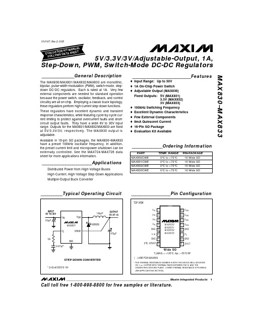
__________Typical Operating Circuit
__________________Pin Configuration
TOP VIEW
INPUT 8V TO 30V 100µF VIN VSW
100µH*
OUTPUT 5V AT 1A
V IN 1 V IN 2 V IN 3
16 V SW 15 V SW 14 V SW
_______________________Applications
Distributed Power from High-Voltage Buses High-Current, High-Voltage Step-Down Applications Multiple-Output Buck Converter
MAX831
VC 10k 0.047µF SENSE
IBM 部分电源控制IC中文引脚说明

MAX1631的引脚说明PIN1:CSH3。
3.3V SMPS(开关电源Switch Mode Power Supply )电流检测输入,以CSL3为参考限流电平为100mV。
PIN2:CSL3。
电流检测输入。
常在固定输出模式里作为反馈输入。
PIN3:FB3。
3.3V SMPS的反馈输入;将FB3调整在REF(约2.5V)时为输出可调模式。
当FB3接地时,为固定3.3V输出。
当FB3连接一个分压电阻时为输出可调节模式。
PIN4:对MAX1630、MAX1632来说,此脚为12V输出。
可往外提供12V,120mA的电压。
但要外接一个1uF电容。
对MAX1631来说,此脚为STEER。
次级反馈的逻辑控制输入。
用来选择PWM采用那路变压器和次级反馈信号。
当STEER为GND时,SECFB(secondary feedback次级反馈采用3.3V 变压器次级反馈。
当STEER为VL时,SECFB采用5V 变压器次级反馈。
PIN5:对MAX1630、MAX1632,VDD。
内置线性12V的电源。
对MAX1631,SECFB,次级线圈反馈输入。
通常从辅助输出连接一个电阻分压器。
SECFB调整在。
当接时为不采用。
2.5V VLPIN6:SYNC,振荡同步和频率选择。
连接到VL时工作在300kHZ;接地工作在200kHZ。
当有外接同步时时钟范围可在240kHZ至350Khz。
PIN7:TIME/ON5,具有双用途,用作定时电容引脚和开关控制输入。
PIN8:GND,低噪音模拟地和反馈参考点。
PIN9:REF,2.5V参考电压输出。
接1uF电容至地。
PIN10:SKIP#。
逻辑控制输入。
当为高电平时取消空闲模式。
接地为正常模式。
PIN11:RESET#,低电平有效的定时复位输出。
RESET#在地至VL之间变化。
在上电后的32,000个周32000期变高电平。
PIN12:FB5,5V SMPS反馈输入;调整到FB5=REF(约2.5V)工作输出可调整模式。
MAX322CPA+中文资料

_______________General DescriptionThe MAX320/MAX321/MAX322 are precision, dual,SPST analog switches designed to operate from ±3V to ±8V dual supplies. The MAX320 has two normally open (NO) switches and the MAX321 has two normally closed (NC) switches. The MAX322 has one NO and one NC switch. Low power consumption (1.25mW)makes these parts ideal for battery-powered equip-ment. They offer low leakage currents (100pA max) and fast switching speeds (t ON = 150ns max, t OFF = 100ns max).The MAX320 series, powered from ±5V supplies, offers 35Ωmax on-resistance (R ON ), 2Ωmax matching between channels, and 4Ωmax R ON flatness.These switches also offer 5pC max charge injection and a minimum of 2000V ESD protection per Method 3015.7.For equivalent devices specified for single-supply oper-ation, see the MAX323/MAX324/MAX325 data sheet.For quad versions of these switches, see the MAX391/MAX392/MAX393 data sheet.________________________ApplicationsBattery-Operated Systems Sample-and-Hold Circuits Heads-Up Displays Guidance and Control Systems Audio and Video Switching Military RadiosTest Equipment Communications Systems ±5V DACs and ADCsPBX, PABX____________________________Featureso Low On-Resistance, 35Ωmax (16Ωtypical)o R ON Matching Between Channels <2Ωo R ON Flatness <4Ωo Guaranteed Charge Injection <5pC o Bipolar Supply Operation (±3V to ±8V)o Low Power Consumption, <1.25mW o Low Leakage Current Over Temperature, <2.5nA at +85°C o Fast Switching, t ON <150ns, t OFF <100ns o Guaranteed Break-Before-Make (MAX322 only)______________Ordering InformationMAX320/MAX321/MAX322Precision, Dual-Supply, SPSTAnalog Switches________________________________________________________________Maxim Integrated Products 1_____________________Pin Configurations/Functional Diagrams/Truth TablesCall toll free 1-800-998-8800 for free samples or literature.19-0350; Rev 0; 12/94* Contact factory for dice specifications.** Contact factory for availability.Voltage Referenced to V-V+................................................................(V- - 0.3V) to +17V IN_, COM_, NC_, NO_ (Note 1).........(V- - 0.3V) to (V+ + 0.3V)Continuous Current (any terminal)......................................30mA Peak Current, COM_, NO_, NC_(pulsed at 1ms, 10% duty cycle max)..............................100mA ESD per Method 3015.7..................................................>2000V Continuous Power DissipationPlastic DIP (derate 9.09mW/°C above +70°C).............727mW Narrow SO (derate 5.88mW/°C above +70°C).............471mWµMAX (derate 4.10mW/°C above +70°C).....................330mW CERDIP (derate 8.00mW/°C above +70°C)..................640mW Operating Temperature RangesMAX32_C_ _........................................................0°C to +70°C MAX32_E_ _......................................................-40°C to +85°C MAX32_MJA...................................................-55°C to +125°C Storage Temperature Range.............................-65°C to +150°C Lead Temperature (soldering, 10sec).............................+300°CM A X 320/M A X 321/M A X 322Precision, Dual-Supply, SPST Analog Switches 2_______________________________________________________________________________________Stresses beyond those listed under “Absolute Maximum Ratings” may cause permanent damage to the device. These are stress ratings only, and functional operation of the device at these or any other conditions beyond those indicated in the operational sections of the specifications is not implied. Exposure to absolute maximum rating conditions for extended periods may affect device reliability.ABSOLUTE MAXIMUM RATINGSNote 1:Signals on NC_, NO_, COM_, or IN_ exceeding V+ or V- are clamped by internal diodes. Limit forward diode current tomaximum current rating.ELECTRICAL CHARACTERISTICS(V+ = +5V ±10%, V- = -5V ±10%, V INH = 3.5V, V INL = 2.5V, T A = T MIN to T MAX , unless otherwise noted.)MAX320/MAX321/MAX322Precision, Dual-Supply, SPSTAnalog Switches_______________________________________________________________________________________3ELECTRICAL CHARACTERISTICS(V+ = +5V ±10%, V- = -5V ±10%, V INH = 3.5V, V INL = 2.5V, T A = T MIN to T MAX , unless otherwise noted.)Note 2:The algebraic convention where the most negative value is a minimum and the most positive value a maximum is used in this data sheet.Note 3:Guaranteed by design.Note 4:∆R ON = ∆R ON max - ∆R ON min.Note 5:Flatness is defined as the difference between the maximum and minimum value of on-resistance as measured over the specified analog signal range.Note 6:Leakage parameters are 100% tested at maximum rated hot temperature and guaranteed by correlation at +25°C.Note 7:Off Isolation = 20 log 10[ V COM ⁄ (V NC or V NO )], V COM = output, V NC or V NO = input to off switch.Note 8:Between any two switches.M A X 320/M A X 321/M A X 322Precision, Dual-Supply, SPST Analog Switches 4_________________________________________________________________________________________________________________________________Typical Operating Characteristics(V+ = +5V, V- = -5V, T A = +25°C, unless otherwise noted.)0.0001-556585OFF LEAKAGE CURRENT vs. TEMPERATURE10TEMPERATURE (°C)O F F L E A K A G E C U R R E N T (n A )-1552545-351051250.10.00110.011000-8-602ON-RESISTANCE vs. VOLTAGE AT COM PIN30V COM (V)R O N (Ω)-4-24682052510150-5-3-4-234ON-RESISTANCE vs. VOLTAGE AT COM PIN(OVER TEMPERATURE)30V COM (V)R O N (Ω)-11252052515100-5-1ON-RESISTANCE MATCH vs. VOLTAGE AT COM PIN (OVER TEMPERATURE)V COM (V)∆R O N (Ω)130.300.350.100.050.400.450.200.250.150.505-30.0001-556585ON LEAKAGE CURRENT vs. TEMPERATURE10TEMPERATURE (°C)O N L E A K A G E C U R R E N T (n A )-1552545-351051250.10.00110.011000-556585SUPPLY CURRENT vs. TEMPERATURE100120M A X 320-07TEMPERATURE (°C)I S U P P L Y (µA )2545-35-15510512580204060140-20-5CHARGE INJECTION vs. VOLTAGE AT COM PIN15M A X 320-06V COM (V)Q (p C )-1050-15105-10-520-4-3-21234MAX320/MAX321/MAX322Precision, Dual-Supply, SPSTAnalog Switches_______________________________________________________________________________________5__________Applications InformationLogic LevelsCalculate the logic thresholds typically as follows: V IH =(V+ - 1.5V) and V IL = (V+ - 2.5V).Power-supply consumption is minimized when IN1 and IN2 are driven with logic-high levels equal to V+ and logic-low levels well below the calculated V IL of (V+ - 2.5V). IN1and IN2 can be driven to V- without damage.Analog Signal LevelsAnalog signals that range over the entire supply voltage (V- to V+) can be switched, with very little change in on-resistance over the entire voltage range (see Typical Operating Characteristics ). All switches are bidirec-tional, so NO_, NC_, and COM_ pins can be used as either inputs or outputs.Power-Supply Sequencing and Overvoltage ProtectionDo not exceed the absolute maximum ratings, because stresses beyond the listed ratings may cause perma-nent damage to the devices.Proper power-supply sequencing is recommended for all CMOS devices. Always apply V+, followed by V-,before applying analog signals or logic inputs, especial-ly if the analog or logic signals are not current-limited. Ifthis sequencing is not possible, and if the analog or logic inputs are not current-limited to <30mA, add two small signal diodes (D1, D2) as shown in Figure 1.Adding protection diodes reduces the analog signal range to a diode drop (about 0.7V) below V+ for D1,and a diode drop above V- for D2. Leakage is not affected by adding the diodes. On-resistance increas-es by a small amount at low supply voltages. Maximum supply voltage (V- to V+) must not exceed 17V.Adding protection diode D1 causes the logic thresh-olds to be shifted relative to the positive power-supply rail. This can be significant when low positive supply voltages (+5V or less) are used. Driving IN1 and IN2 all the way to the supply rails (i.e., to a diode drop higher than the V+ pin or a diode drop lower than the V- pin) is always acceptable.The protection diodes D1 and D2 also protect against some overvoltage situations. With the circuit of Figure 1,if the supply voltage is below the absolute maximum rating and if a fault voltage up to the absolute maximum rating is applied to an analog signal pin, no damage will result. For example, with ±5V supplies, analog sig-nals up to ±8.5V will not damage the circuit of Figure 1.If only a single fault signal is present, the fault voltage can rise to +12V or to -12V without damage._____________________Pin DescriptionFigure 1. Overvoltage Protection Using Two External Blocking DiodesM A X 320/M A X 321/M A X 322Precision, Dual-Supply, SPST Analog Switches 6_______________________________________________________________________________________Figure 4. Charge InjectionFigure 2. Switching TimeFigure 3. Break-Before-Make Interval (MAX322 only)______________________________________________Test Circuits/Timing DiagramsMAX320/MAX321/MAX322Precision, Dual-Supply, SPSTAnalog Switches_______________________________________________________________________________________7Figure 6. Crosstalk_________________________________Test Circuits/Timing Diagrams (continued)Figure 8. Channel-On CapacitanceFigure 7. Channel-Off Capacitance__Ordering Information (continued)___________________Chip Topography0.075" (1.90mm)0.055" (1.40mm)V+ IN2V-IN1COM2NO2 (MAX320) NC2 (MAX321/2)COM1NO1 (MAX320/2) NC1 (MAX321)* Contact factory for dice specifications.** Contact factory for availability.TRANSISTOR COUNT: 91SUBSTRATE CONNECTED TO V+M A X 320/M A X 321/M A X 322Precision, Dual-Supply, SPST Analog Switches________________________________________________________Package Informationimplied. Maxim reserves the right to change the circuitry and specifications without notice at any time.8___________________Maxim Integrated Products, 120 San Gabriel Drive, Sunnyvale, CA 94086 (408) 737-7600©1994 Maxim Integrated ProductsPrinted USAis a registered trademark of Maxim Integrated Products.。
MAX3280EAUK+T中文资料

Features
o ESD Protection: ±15kV–Human Body Model ±6kV–IEC 1000-4-2, Contact Discharge ±12kV–IEC 1000-4-2, Air-Gap Discharge
o Guaranteed 52Mbps Data Rate o Guaranteed 15ns Receiver Propagation Delay o Guaranteed 2ns Receiver Skew o Guaranteed 8ns Package-to-Package Skew Time o VL Pin for Connection to FPGAs/ASICs o Allow Up to 128 Transceivers on the Bus
Receiver Output Voltage (RO)....................-0.3V to (VCC + 0.3V) Receiver Output Voltage
(RO) (MAX3284E) .....................................-0.3V to (VL + 0.3V) Receiver Output Short-Circuit Current .......................Continuous
ENABLE —
Active High Active Low
—
DATA RATE 52Mbps 52Mbps 52Mbps
52Mbps (Note 1)
PACKAGE 5-Pin SOT23 6-Pin SOT23 6-Pin SOT23 6-Pin SOT23
________________________________________________________________ Maxim Integrated Products 1
MAX6133中文资料
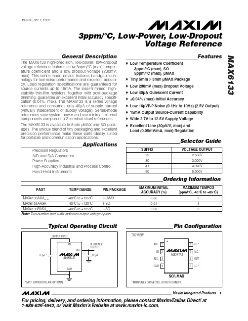
General DescriptionThe MAX6133 high-precision, low-power, low-dropout voltage reference features a low 3ppm/°C (max) temper-ature coefficient and a low dropout voltage (200mV,max). This series-mode device features bandgap tech-nology for low-noise performance and excellent accura-cy. Load regulation specifications are guaranteed for source currents up to 15mA. The laser-trimmed, high-stability thin-film resistors, together with post-package trimming, guarantee an excellent initial accuracy specifi-cation (0.04%, max). The MAX6133 is a series voltage reference and consumes only 40µA of supply current (virtually independent of supply voltage). Series-mode references save system power and use minimal external components compared to 2-terminal shunt references.The MAX6133 is available in 8-pin µMAX and SO pack-ages. The unique blend of tiny packaging and excellent precision performance make these parts ideally suited for portable and communication applications.ApplicationsPrecision Regulators A/D and D/A Converters Power SuppliesHigh-Accuracy Industrial and Process Control Hand-Held InstrumentsFeatureso Low Temperature Coefficient3ppm/°C (max), SO 5ppm/°C (max), µMAX o Tiny 5mm ✕3mm µMAX Package o Low 200mV (max) Dropout Voltage o Low 40µA Quiescent Current o ±0.04% (max) Initial Accuracyo Low 16µV P-P Noise (0.1Hz to 10Hz) (2.5V Output)o 15mA Output Source-Current Capability o Wide 2.7V to 12.6V Supply Voltage o Excellent Line (30µV/V, max) and Load (0.05mV/mA, max) RegulationMAX61333ppm/°C, Low-Power, Low-DropoutVoltage Reference________________________________________________________________Maxim Integrated Products 1Pin ConfigurationOrdering InformationTypical Operating Circuit19-2266; Rev 1; 12/02For pricing, delivery, and ordering information,please contact Maxim/Dallas Direct!at 1-888-629-4642, or visit Maxim’s website at .Note:Two-number part suffix indicates output voltage option.Selector GuideM A X 61333ppm/°C, Low-Power, Low-Dropout Voltage Reference 2_______________________________________________________________________________________ABSOLUTE MAXIMUM RATINGSELECTRICAL CHARACTERISTICS —MAX6133_25 (V OUT = 2.500V)Stresses beyond those listed under “Absolute Maximum Ratings” may cause permanent damage to the device. These are stress ratings only, and functional operation of the device at these or any other conditions beyond those indicated in the operational sections of the specifications is not implied. Exposure to absolute maximum rating conditions for extended periods may affect device reliability.Voltage (with Respect to GND)IN........................................................................-0.3V to +13V OUT..............................................-0.3V to +6V or (V IN + 0.3V)OUT Short Circuit to IN or GND Duration...............................60s Continuous Power Dissipation (T A = +70°C)8-Pin µMAX (derate 5.5mW/°C above +70°C).............362mW 8-Pin SO (derate 5.88mW/°C above +70°C)................471mWOperating Temperature Range .........................-40°C to +125°C Storage Temperature Range.............................-65°C to +150°C Junction Temperature......................................................+150°C Lead Temperature (soldering, 10s).................................+300°CMAX61333ppm/°C, Low-Power, Low-DropoutVoltage Reference_______________________________________________________________________________________3ELECTRICAL CHARACTERISTICS —MAX6133_30 (V OUT = 3.0000V)(V IN = 5V, C LOAD = 0.1µF, I OUT = 0, T A = T MIN to T MAX . Typical values are at T A = +25°C, unless otherwise noted.)M A X 61333ppm/°C, Low-Power, Low-Dropout Voltage Reference 4_______________________________________________________________________________________ELECTRICAL CHARACTERISTICS —MAX6133_41 (V OUT = 4.096V)MAX61333ppm/°C, Low-Power, Low-DropoutVoltage Reference_______________________________________________________________________________________5ELECTRICAL CHARACTERISTICS —MAX6133_50 (V OUT = 5.000V)Note 2:Dropout Voltage is the minimum voltage at which V OUT changes ≤0.1% from V OUT at V IN = 5V (V IN = 5.5V for V OUT = 5V).Note 3:Thermal Hysteresis is defined as the change in the initial +25°C output voltage after cycling the device from T MAX to T MIN .M A X 61333ppm/°C, Low-Power, Low-Dropout Voltage Reference 6_______________________________________________________________________________________Typical Operating Characteristics(V IN = 5V, I OUT = 0, T A = +25°C, unless otherwise noted.) (Note 4)SUPPLY CURRENT vs. INPUT VOLTAGE(V OUT = 2.5V)INPUT VOLTAGE (V)S U P P L Y C U R R E N T (µA )1211910345678121530456075901051201351500013-120-80-100-60-40-2000.00010.010.0010.1101001000POWER-SUPPLY REJECTION RATIO vs. FREQUENCY (V OUT = 5V)FREQUENCY (kHz)P S R R (d B )1POWER-SUPPLY REJECTION RATIO vs. FREQUENCY (V OUT = 2.5V)FREQUENCY (kHz)0.00010.1101000.0010.011000P S R R (d B )0-120-100-80-60-40-20M A X 6133 t o c 071DROPOUT VOLTAGE vs. OUTPUT CURRENT(V OUT = 5V)OUTPUT CURRENT (mA)D RO P O U T V O L T A G E (m V )1816121446810250100150200250300350400450500550600020DROPOUT VOLTAGE vs. OUTPUT CURRENT(V OUT = 2.5V)OUTPUT CURRENT (mA)D R O P O U T V O L T A GE (m V )181********642100200300400500600700020LOAD REGULATION (V OUT = 5V)OUTPUT CURRENT (mA)O U T P U T V O L T A G E (V )182461012148164.99854.99904.99955.00005.00055.00105.00155.00204.998020LOAD REGULATION (V OUT = 2.5V)OUTPUT CURRENT (mA)O U T P U T V O L T A G E (V )20181416468101222.50052.50102.49902.49952.50002.50152.50202.50252.50302.50352.50400OUTPUT VOLTAGE vs. TEMPERATURE(V OUT = 5V)TEMPERATURE (°C)O U T P U T V O L T A G E (V )110956580-105203550-254.99854.99904.99955.00005.00055.00104.9980-40125OUTPUT VOLTAGE vs. TEMPERATURE(V OUT = 2.5V)TEMPERATURE (°C)O U T P U T V O L T A G E (V )110956580-105203550-252.49942.49962.49982.50002.50022.50042.50062.50082.50102.4992-40125MAX61333ppm/°C, Low-Power, Low-DropoutVoltage Reference_______________________________________________________________________________________7Typical Operating Characteristics (continued)(V IN = 5V, I OUT = 0, T A = +25°C, unless otherwise noted.) (Note 4)LOAD TRANSIENT (V OUT = 2.5V)MAX6133 toc152.5V0mA10mA I OUT10mA/divV OUT 50mV/div AC-COUPLED400µs/divC OUT = 10µFLOAD TRANSIENT (V OUT = 2.5V)2.5V-100µA1mA 1ms/divI OUT 1mA/divV OUT 50mV/div AC-COUPLEDC OUT = 0.1µFLOAD TRANSIENT (V OUT = 2.5V)2.5V0mA10mA I OUT10mA/divV OUT 50mV/div AC-COUPLED400µs/divC OUT = 0.1µF0.1Hz TO 10Hz OUTPUT NOISE(V OUT = 5V)V OUT 10µV/div1s/divV IN = 5.5V0.1Hz TO 10Hz OUTPUT NOISE(V OUT = 2.5V)MAX6133 toc11V OUT 4µV/div1s/divSUPPLY CURRENT vs. INPUT VOLTAGE(V OUT = 5V)INPUT VOLTAGE (V)S U P P L Y C U R R E N T (µA )12119103456781220406080100120140160180200220013M A X 61333ppm/°C, Low-Power, Low-Dropout Voltage Reference 8_______________________________________________________________________________________Typical Operating Characteristics (continued)(V IN = 5V, I OUT = 0, T A = +25°C, unless otherwise noted.) (Note 4)TURN-ON TRANSIENT (V OUT = 2.5V)5V0V2.5VV OUT 1V/divV IN 2V/div2ms/divC OUT = 10µF0VTURN-ON TRANSIENT(V OUT = 5V)MAX6133 toc205.5V0V5VV OUT 2V/divV IN 2V/div400µs/divV IN = 5.5V C OUT = 0.1µF0VTURN-ON TRANSIENT (V OUT = 2.5V)MAX6133 toc195V0V2.5VV OUT 1V/divV IN 2V/div100µs/div0V C OUT = 0.1µFLINE TRANSIENT (V OUT = 5V)6.5V5V5.5VV OUT 10mV/div AC-COUPLEDV IN500mV/div AC-COUPLED1ms/divC OUT = 0.1µFV IN = 5.5VLINE TRANSIENT (V OUT = 2.5V)5.5V2.5V4.5VV OUT 10mV/div AC-COUPLEDV IN500mV/div AC-COUPLED400µs/divC OUT = 0.1µFLOAD TRANSIENT (V OUT = 2.5V)2.5V-100µA1mA I OUT 1mA/divV OUT 20mV/div AC-COUPLED1ms/divC OUT = 10µFMAX61333ppm/°C, Low-Power, Low-DropoutVoltage Reference_______________________________________________________________________________________9TURN-ON TRANSIENT(V OUT = 5V)5.5V0V5VV OUT 2V/divV IN 2V/div2ms/div0V2.50012.50032.50022.50052.50042.50072.50062.500804002006008001005003007009001000LONG-TERM STABILITY vs. TIME(V OUT = 2.5V)TIME (HOURS)V O U T (V ) 2.49942.50002.49982.50042.50022.50082.50062.501004002006008001005003007009001000LONG-TERM STABILITY vs. TIME(V OUT= 2.5V)TIME (HOURS)V O U T (V )2.49965.00005.00035.00025.00055.00045.00075.00065.000804002006008001005003007009001000LONG-TERM STABILITY vs. TIME(V OUT = 5.0V)TIME (HOURS)V O U T (V )5.00014.99994.99984.99974.9996 5.00045.00085.00105.00125.001404002006008001005003007009001000LONG-TERM STABILITY vs. TIME(V OUT= 5.0V)TIME (HOURS)V O U T (V )5.00065.00025.0000Note 4:Many of the MAX6133 Typical Operating Characteristics are extremely similar. The extremes of these characteristics arefound in the MAX6133 (2.5V output) and the MAX6133 (5V output). The Typical Operating Characteristics of the remainder of the MAX6133 family typically lie between these two extremes and can be estimated based on their output voltages.Typical Operating Characteristics (continued)(V IN = 5V, I OUT = 0, T A = +25°C, unless otherwise noted.) (Note 4)M A X 61333ppm/°C, Low-Power, Low-Dropout Voltage Reference 10______________________________________________________________________________________Applications InformationBypassing/Load CapacitanceFor the best line-transient performance, decouple the input with a 0.1µF ceramic capacitor as shown in the Typical Operating Circuit . Place the capacitor as close to I N as possible. When transient performance is less important, no capacitor is necessary. The MAX6133family requires a minimum output capacitance of 0.1µF for stability and is stable with capacitive loads (includ-ing the bypass capacitance) of up to 100µF. In applica-tions where the load or the supply can experience step changes, a larger output capacitor reduces the amount of overshoot (undershoot) and improves the circuit ’s transient response. Place output capacitors as close to the device as possible.Supply CurrentThe quiescent supply current of the MAX6133 series reference is typically 40µA and is virtually independent of the supply voltage. In the MAX6133 family, the load current is drawn from the input only when required, so supply current is not wasted and efficiency is maxi-mized at all input voltages. This improved efficiency reduces power dissipation and extends battery life.When the supply voltage is below the minimum-speci-fied input voltage (as during turn-on), the devices can draw up to 150µA beyond the nominal supply current.The input voltage source must be capable of providing this current to ensure reliable turn-on.Thermal HysteresisThermal hysteresis is the change in the output voltage at T A = +25°C before and after the device is cycled over its entire operating temperature range. Hysteresis is caused by differential package stress appearing across the bandgap core transistors. The typical ther-mal hysteresis value is 120ppm for both SO and µMAX packages.Turn-On TimeThese devices typically turn on and settle to within 0.01% of their final value in <1ms. The turn-on time can increase up to 2ms with the device operating at the minimum dropout voltage and the maximum load.Low-Power, 14-Bit DACwith MAX6133 as a ReferenceFigure 1 shows a typical application circuit for the MAX6133 providing both the power supply and precision reference voltage for a 14-bit high-resolution, serial-input, voltage-output digital-to-analog converter. The MAX6133 with a 2.5V output provides the reference volt-age for the DAC.Figure 1. 14-Bit High-Resolution DAC and Positive Reference From a Single 3V SupplyMAX61333ppm/°C, Low-Power, Low-DropoutVoltage Reference______________________________________________________________________________________11Figure 3. Temperature Coefficient vs. Operating Temperature Range for a 1LSB Maximum ErrorNegative Low-Power Voltage ReferenceAs shown in Figure 2, the MAX6133 can be used to develop a negative voltage reference using the MAX400, a rail-to-rail op-amp with low power, low noise, and low offset. The circuit only provides a good negative reference and is ideal for space- and cost-sensitive applications since it does not use resistors.Temperature Coefficient vs.Operating Temperature Rangefor a 1LSB Maximum ErrorI n a data converter application, the converter ’s refer-ence voltage must stay within a certain limit to keep the error in the data converter smaller than the resolution limit through the operating temperature range. Figure 3shows the maximum allowable reference-voltage tem-perature coefficient that keeps the conversion error to less than 1LSB. This is a function of the operating tem-perature range (T MAX - T MIN ) with the converter resolu-tion as a parameter. The graph assumes the reference-voltage temperature coefficient as the only parameter affecting accuracy. I n reality, the absolute static accuracy of a data converter is dependent on the combination of many parameters such as integral non-linearity, differential nonlinearity, offset error, gain error,as well as voltage reference changes.Chip InformationTRANSISTOR COUNT: 656PROCESS: BiCMOSFigure 2. Negative Low-Power Voltage ReferenceM A X 61333ppm/°C, Low-Power, Low-Dropout Voltage Reference 12______________________________________________________________________________________Package Information(The package drawing(s) in this data sheet may not reflect the most current specifications. For the latest package outline information,go to /packages .)MAX61333ppm/°C, Low-Power, Low-DropoutVoltage ReferenceMaxim c annot assume responsibility for use of any c irc uitry other than c irc uitry entirely embodied in a Maxim produc t. No c irc uit patent lic enses are implied. Maxim reserves the right to change the circuitry and specifications without notice at any time.Maxim Integrated Products, 120 San Gabriel Drive, Sunnyvale, CA 94086 408-737-7600 ____________________13©2002 Maxim Integrated ProductsPrinted USAis a registered trademark of Maxim Integrated Products.Package Information (continued)(The package drawing(s) in this data sheet may not reflect the most current specifications. For the latest package outline information,go to /packages .)。
MAX6318MHUK50AZ-T中文资料
___________________________________________________________________Selector Guide________________General DescriptionThe MAX6316–MAX6322 family of microprocessor (µP)supervisory circuits monitors power supplies and microprocessor activity in digital systems. It offers sev-eral combinations of push/pull, open-drain, and bidirec-tional (such as Motorola 68HC11) reset outputs, along with watchdog and manual reset features. The Selector Guide below lists the specific functions available from each device. These devices are specifically designed to ignore fast negative transients on V CC . Resets are guaranteed valid for V CC down to 1V.These devices are available in 26 factory-trimmed reset threshold voltages (from 2.5V to 5V, in 100mV incre-ments), featuring four minimum power-on reset timeout periods (from 1ms to 1.12s), and four watchdog timeout periods (from 6.3ms to 25.6s). Thirteen standard ver-sions are available with an order increment requirement of 2500 pieces (see Standard Versions table); contact the factory for availability of other versions, which have an order increment requirement of 10,000 pieces.The MAX6316–MAX6322 are offered in a miniature 5-pin SOT23 package.________________________ApplicationsPortable Computers Computers ControllersIntelligent InstrumentsPortable/Battery-Powered Equipment Embedded Control Systems____________________________Features♦Small 5-Pin SOT23 Package♦Available in 26 Reset Threshold Voltages2.5V to 5V, in 100mV Increments ♦Four Reset Timeout Periods1ms, 20ms, 140ms, or 1.12s (min)♦Four Watchdog Timeout Periods6.3ms, 102ms, 1.6s, or 25.6s (typ) ♦Four Reset Output StagesActive-High, Push/Pull Active-Low, Push/Pull Active-Low, Open-Drain Active-Low, Bidirectional♦Guaranteed Reset Valid to V CC = 1V♦Immune to Short Negative V CC Transients ♦Low Cost♦No External ComponentsMAX6316–MAX63225-Pin µP Supervisory Circuits withWatchdog and Manual Reset________________________________________________________________Maxim Integrated Products 119-0496; Rev 7; 11/07_______________Ordering InformationOrdering Information continued at end of data sheet.*The MAX6318/MAX6319/MAX6321/MAX6322 feature two types of reset output on each device.Typical Operating Circuit and Pin Configurations appear at end of data sheet.For pricing, delivery, and ordering information, please contact Maxim Direct at 1-888-629-4642,or visit Maxim’s website at .Specify lead-free by replacing “-T” with “+T” when ordering.ELECTRICAL CHARACTERISTICS(V CC = 2.5V to 5.5V, T A = -40°C to +125°C, unless otherwise noted. Typical values are at T A = +25°C.) (Note 1)M A X 6316–M A X 63225-Pin µP Supervisory Circuits with Watchdog and Manual Reset 2_______________________________________________________________________________________ABSOLUTE MAXIMUM RATINGSStresses beyond those listed under “Absolute Maximum Ratings” may cause permanent damage to the device. These are stress ratings only, and functional operation of the device at these or any other conditions beyond those indicated in the operational sections of the specifications is not implied. Exposure to absolute maximum rating conditions for extended periods may affect device reliability.Voltage (with respect to GND)V CC ......................................................................-0.3V to +6V RESET (MAX6320/MAX6321/MAX6322 only)...... -0.3V to +6V All Other Pins.........................................-0.3V to (V CC + 0.3V)Input/Output Current, All Pins.............................................20mAContinuous Power Dissipation (T A = +70°C)SOT23-5 (derate 7.1mW/°C above +70°C)...............571mW Operating Temperature Range..........................-40°C to +125°C Junction Temperature......................................................+150°C Storage Temperature Range..............................-65°C to +160°C Lead Temperature (soldering, 10s).................................+300°CTH available in 100mV increments from 2.5V to 5V (see Table 1 at end of data sheet).Note 3:Guaranteed by design.MAX6316–MAX63225-Pin µP Supervisory Circuits withWatchdog and Manual Reset_______________________________________________________________________________________3Note 5:Measured from RESET V OL to (0.8 x V CC ), R LOAD = ∞.Note 6:WDI is internally serviced within the watchdog period if WDI is left unconnected.Note 7:The WDI input current is specified as the average input current when the WDI input is driven high or low. The WDI input is designed for a three-stated-output device with a 10µA maximum leakage current and capable of driving a maximum capac-itive load of 200pF. The three-state device must be able to source and sink at least 200µA when active.ELECTRICAL CHARACTERISTICS (continued)M A X 6316–M A X 63225-Pin µP Supervisory Circuits with Watchdog and Manual Reset 4_________________________________________________________________________________________________________________________________Typical Operating Characteristics(T A = +25°C, unless otherwise noted.)021*********-4020-20406080100MAX6316/MAX6317/MAX6318/MAX6320/MAX6321SUPPLY CURRENT vs. TEMPERATURETEMPERATURE (°C)S U P P L Y C U R R E N T (μA )302010504090807060100-40-20020406080100V CC FALLING TO RESET PROPAGATIONDELAY vs. TEMPERATURETEMPERATURE (°C)R E S E T P R O P A G A T I O N D E L A Y (μs )140180160240220200300280260320-40020-20406080100MAX6316/MAX6317/MAX6319/MAX6320/MAX6322MANUAL RESET TO RESETPROPAGATION DELAY vs. TEMPERATURETEMPERATURE (°C)P R O P A G A T I O N D E L A Y (n s )0.950.980.970.961.000.991.041.031.021.011.05-40-2020406080100NORMALIZED RESET TIMEOUT PERIOD vs. TEMPERATUREM A X 6316t o c 04TEMPERATURE (°C)N O R M A L I Z E D R E S E T T I M E O U T P E R I O D0.950.980.970.961.000.991.041.031.021.011.05-40-2020406080100MAX6316/MAX6317/MAX6318/MAX6320/MAX6321NORMALIZED WATCHDOG TIMEOUTPERIOD vs. TEMPERATUREM A X 6316t o c 05TEMPERATURE (°C)N O R M A L I Z E D W A T C H D O G T I M E O U T P E R I O D800101001000MAXIMUM V CC TRANSIENT DURATION vs. RESET THRESHOLD OVERDRIVE2010RESET THRESHOLD OVERDRIVE (mV) V RST - V CCT RA N S I E N T D U R A T I O N (μs )3050604070200ns/divMAX6316M/6318MH/6319MHBIDIRECTIONALPULLUP CHARACTERISTICSMAX6316–MAX63225-Pin µP Supervisory Circuits withWatchdog and Manual Reset_______________________________________________________________________________________5______________________________________________________________Pin DescriptionM A X 6316–M A X 63225-Pin µP Supervisory Circuits with Watchdog and Manual Reset 6______________________________________________________________________________________________________Detailed DescriptionA microprocessor’s (µP) reset input starts or restarts the µP in a known state. The reset output of the MAX6316–MAX6322 µP supervisory circuits interfaces with the reset input of the µP, preventing code-execution errors during power-up, power-down, and brownout condi-tions (see the Typical Operating Circuit ). The MAX6316/MAX6317/MAX6318/MAX6320/MAX6321 are also capa-ble of asserting a reset should the µP become stuck in an infinite loop.Reset OutputThe MAX6316L/MAX6318LH/MAX6319LH feature an active-low reset output, while the MAX6317H/MAX6318_H/MAX6319_H/MAX6321HP/MAX6322HP feature an active-high reset output. RESET is guaran-teed to be a logic low and RESET is guaranteed to be a logic high for V CC down to 1V.The MAX6316–MAX6322 assert reset when V CC is below the reset threshold (V RST ), when MR is pulled low (MAX6316_/MAX6317H/MAX6319_H/MAX6320P/MAX6322HP only), or if the WDI pin is not serviced withinthe watchdog timeout period (t WD ). Reset remains assert-ed for the specified reset active timeout period (t RP ) after V CC rises above the reset threshold, after MR transitions low to high, or after the watchdog timer asserts the reset (MAX6316_/MAX6317H/MAX6318_H/MAX6320P/MAX6321HP). After the reset active timeout period (t RP )expires, the reset output deasserts, and the watchdog timer restarts from zero (Figure 2).Figure 1. Functional DiagramFigure 2. Reset Timing DiagramMAX6316–MAX63225-Pin µP Supervisory Circuits withWatchdog and Manual Reset_______________________________________________________________________________________7Bidirectional R E S E T OutputThe MAX6316M/MAX6318MH/MAX6319MH are designed to interface with µPs that have bidirectional reset pins,such as the Motorola 68HC11. Like an open-drain output,these devices allow the µP or other devices to pull the bidirectional reset (RESET ) low and assert a reset condi-tion. However, unlike a standard open-drain output, it includes the commonly specified 4.7k Ωpullup resistor with a P-channel active pullup in parallel.This configuration allows the MAX6316M/MAX6318MH/MAX6319MH to solve a problem associated with µPs that have bidirectional reset pins in systems where sev-eral devices connect to RESET (F igure 3). These µPs can often determine if a reset was asserted by an exter-nal device (i.e., the supervisor IC) or by the µP itself (due to a watchdog fault, clock error, or other source),and then jump to a vector appropriate for the source of the reset. However, if the µP does assert reset, it does not retain the information, but must determine the cause after the reset has occurred.The following procedure describes how this is done in the Motorola 68HC11. In all cases of reset, the µP pulls RESET low for about four external-clock cycles. It then releases RESET , waits for two external-clock cycles,then checks RESET ’s state. If RESET is still low, the µP concludes that the source of the reset was external and, when RESET eventually reaches the high state, it jumps to the normal reset vector. In this case, stored-state information is erased and processing begins fromscratch. If, on the other hand, RESET is high after a delay of two external-clock cycles, the processor knows that it caused the reset itself and can jump to a different vector and use stored-state information to determine what caused the reset.A problem occurs with faster µPs; two external-clock cycles are only 500ns at 4MHz. When there are several devices on the reset line, and only a passive pullup resis-tor is used, the input capacitance and stray capacitance can prevent RESET from reaching the logic high state (0.8✕V CC ) in the time allowed. If this happens, all resets will be interpreted as external. The µP output stage is guaran-teed to sink 1.6mA, so the rise time can not be reduced considerably by decreasing the 4.7k Ωinternal pullup resistance. See Bidirectional Pullup Characteristics in the Typical Operating Characteristics .The MAX6316M/MAX6318MH/MAX6319MH overcome this problem with an active pullup FET in parallel with the 4.7k Ωresistor (F igures 4 and 5). The pullup transistor holds RESET high until the µP reset I/O or the supervisory circuit itself forces the line low. Once RESET goes below V PTH , a comparator sets the transition edge flip-flop, indi-cating that the next transition for RESET will be low to high. When RESET is released, the 4.7k Ωresistor pulls RESET up toward V CC . Once RESET rises above V PTH but is below (0.85 x V CC ), the active P-channel pullup turns on. Once RESET rises above (0.85 x V CC ) or the 2µs one-shot times out, the active pullup turns off. The parallel combination of the 4.7k Ωpullup and theFigure 3. MAX6316M/MAX6318MH/MAX6319MH Supports Additional Devices on the Reset BusM A X 6316–M A X 63225-Pin µP Supervisory Circuits with Watchdog and Manual Reset 8_______________________________________________________________________________________Figure 4. MAX6316/MAX6318MH/MAX6319MH Bidirectional Reset Output Functional DiagramMAX6316–MAX63225-Pin µP Supervisory Circuits withWatchdog and Manual Reset_______________________________________________________________________________________9P-channel transistor on-resistance quickly charges stray capacitance on the reset line, allowing RESET to transition from low to high within the required two elec-tronic-clock cycles, even with several devices on the reset line. This process occurs regardless of whether the reset was caused by V CC dipping below the reset threshold, the watchdog timing out, MR being asserted,or the µP or other device asserting RESET . The parts do not require an external pullup. To minimize supply cur-rent consumption, the internal 4.7k Ωpullup resistor dis-connects from the supply whenever the MAX6316M/MAX6318MH/MAX6319MH assert reset.Open-Drain R E S E T OutputThe MAX6320P/MAX6321HP/MAX6322HP have an active-low, open-drain reset output. This output struc-ture will sink current when RESET is asserted. Connect a pullup resistor from RESET to any supply voltage up to 6V (Figure 6). Select a resistor value large enough toregister a logic low (see Electrical Characteristics ), and small enough to register a logic high while supplying all input current and leakage paths connected to the RESET line. A 10k Ωpullup is sufficient in most applications.Manual-Reset InputThe MAX6316_/MAX6317H/MAX6319_H/MAX6320P/MAX6322HP feature a manual reset input. A logic low on MR asserts a reset. After MR transitions low to high, reset remains asserted for the duration of the reset timeout peri-od (t RP ). The MR input is connected to V CC through an internal 52k Ωpullup resistor and therefore can be left unconnected when not in use. MR can be driven with TTL-logic levels in 5V systems, with CMOS-logic levels in 3V systems, or with open-drain or open-collector output devices. A normally-open momentary switch from MR to ground can also be used; it requires no external debouncing circuitry. MR is designed to reject fast, negative-going transients (typically 100ns pulses). A 0.1µF capacitor from MR to ground provides additional noise immunity.The MR input pin is equipped with internal ESD-protection circuitry that may become forward biased. Should MR be driven by voltages higher than V CC , excessive current would be drawn, which would damage the part. F or example, assume that MR is driven by a +5V supply other than V CC . If V CC drops lower than +4.7V, MR ’s absolute maximum rating is violated [-0.3V to (V CC + 0.3V)], and undesirable current flows through the ESD structure from MR to V CC . To avoid this, use the same supply for MR as the supply monitored by V CC . This guarantees that the voltage at MR will never exceed V CC .Watchdog InputThe MAX6316_/MAX6317H/MAX6318_H/MAX6320P/MAX6321HP feature a watchdog circuit that monitors the µP’s activity. If the µP does not toggle the watchdog input (WDI) within the watchdog timeout period (t WD ),reset asserts. The internal watchdog timer is cleared by reset or by a transition at WDI (which can detect pulses as short as 50ns). The watchdog timer remains cleared while reset is asserted. Once reset is released, the timer begins counting again (Figure 7).The WDI input is designed for a three-stated output device with a 10µA maximum leakage current and the capability of driving a maximum capacitive load of 200pF.The three-state device must be able to source and sink at least 200µA when active. Disable the watchdog function by leaving WDI unconnected or by three-stating the driver connected to WDI. When the watchdog timer is left open circuited, the timer is cleared internally at intervals equal to 7/8 of the watchdog period.Figure 6. MAX6320P/MAX6321HP/MAX6322HP Open-Drain RESET Output Allows Use with Multiple SuppliesFigure 5. Bidirectional RESET Timing DiagramM A X 6316–M A X 63225-Pin µP Supervisory Circuits with Watchdog and Manual Reset 10______________________________________________________________________________________Applications InformationWatchdog Input CurrentThe WDI input is internally driven through a buffer and series resistor from the watchdog counter. For minimum watchdog input current (minimum overall power con-sumption), leave WDI low for the majority of the watch-dog timeout period. When high, WDI can draw as much as 160µA. Pulsing WDI high at a low duty cycle will reduce the effect of the large input current. When WDI is left unconnected, the watchdog timer is serviced within the watchdog timeout period by a low-high-low pulse from the counter chain.Negative-Going V CC TransientsThese supervisors are immune to short-duration, nega-tive-going V CC transients (glitches), which usually do not require the entire system to shut down. Typically,200ns large-amplitude pulses (from ground to V CC ) on the supply will not cause a reset. Lower amplitude puls-es result in greater immunity. Typically, a V CC transient that goes 100mV under the reset threshold and lasts less than 4µs will not trigger a reset. An optional 0.1µF bypass capacitor mounted close to V CC provides addi-tional transient immunity.Ensuring Valid Reset OutputsDown to V CC = 0The MAX6316_/MAX6317H/MAX6318_H/MAX6319_H/MAX6321HP/MAX6322HP are guaranteed to operate properly down to V CC = 1V. In applications that require valid reset levels down to V CC = 0, a pulldown resistor to active-low outputs (push/pull and bidirectional only,F igure 8) and a pullup resistor to active-high outputs(push/pull only, Figure 9) will ensure that the reset line is valid while the reset output can no longer sink orsource current. This scheme does not work with the open-drain outputs of the MAX6320/MAX6321/MAX6322.The resistor value used is not critical, but it must be large enough not to load the reset output when V CC is above the reset threshold. F or most applications,100k Ωis adequate.Watchdog Software Considerations(MAX6316/MAX6317/MAX6318/MAX6320/MAX6321)One way to help the watchdog timer monitor software execution more closely is to set and reset the watchdog input at different points in the program, rather than pulsing the watchdog input high-low-high or low-high-low. This technique avoids a stuck loop, in which the watchdog timer would continue to be reset inside the loop, keeping the watchdog from timing out.Figure 7. Watchdog Timing RelationshipFigure 9. Ensuring RESET Valid to V CC = 0 on Active-High Push/Pull OutputsFigure 8. Ensuring RESET Valid to V CC = 0 on Active-Low Push/Pull and Bidirectional OutputsMAX6316–MAX6322Watchdog and Manual Reset______________________________________________________________________________________11F igure 10 shows an example of a flow diagram where the I/O driving the watchdog input is set high at the beginning of the program, set low at the end of every subroutine or loop, then set high again when the pro-gram returns to the beginning. If the program should hang in any subroutine, the problem would be quickly corrected, since the I/O is continually set low and the watchdog timer is allowed to time out, causing a reset or interrupt to be issued. As described in the Watchdog Input Current section, this scheme results in higher time average WDI current than does leaving WDI low for the majority of the timeout period and periodically pulsing it low-high-low.Figure 10. Watchdog Flow Diagram__________________Pin ConfigurationsTypical Operating CircuitTable 2. Standard VersionsTable 1. Factory-Trimmed Reset ThresholdsM A X 6316–M A X 6322Watchdog and Manual ResetTable 3. Reset/Watchdog Timeout PeriodsMAX6316–MAX6322Watchdog and Manual Reset______________________________________________________________________________________13__Ordering Information (continued)a watchdog feature (see Selector Guide) are factory-trimmed to one of four watchdog timeout periods. Insert the letter corre-sponding to the desired watchdog timeout period (W, X, Y, or Z from Table 3) into the blank following the reset timeout suffix.TRANSISTOR COUNT: 191SUBSTRATE IS INTERNALLY CONNECTED TO V+Chip Informationdard versions only. The required order increment for nonstandard versions is 10,000 pieces. Contact factory for availability.M A X 6316–M A X 6322Watchdog and Manual Reset 14______________________________________________________________________________________Package Information(The package drawing(s) in this data sheet may not reflect the most current specifications. For the latest package outline information,go to /packages .)M axim cannot assume responsibility for use of any circuitry other than circuitry entirely embodied in a M axim product. No circuit patent licenses are implied. Maxim reserves the right to change the circuitry and specifications without notice at any time.Maxim Integrated Products, 120 San Gabriel Drive, Sunnyvale, CA 94086 408-737-7600 ____________________15©2007 Maxim Integrated Productsis a registered trademark of Maxim Integrated Products, Inc.MAX6316–MAX6322 Watchdog and Manual ResetRevision History。
MAX485CPA+中文资料
For pricing, delivery, and ordering information,please contact Maxim/Dallas Direct!at 1-888-629-4642, or visit Maxim’s website at .General DescriptionThe MAX481, MAX483, MAX485, MAX487–MAX491, and MAX1487 are low-power transceivers for RS-485 and RS-422 communication. Each part contains one driver and one receiver. The MAX483, MAX487, MAX488, and MAX489feature reduced slew-rate drivers that minimize EMI and reduce reflections caused by improperly terminated cables,thus allowing error-free data transmission up to 250kbps.The driver slew rates of the MAX481, MAX485, MAX490,MAX491, and MAX1487 are not limited, allowing them to transmit up to 2.5Mbps.These transceivers draw between 120µA and 500µA of supply current when unloaded or fully loaded with disabled drivers. Additionally, the MAX481, MAX483, and MAX487have a low-current shutdown mode in which they consume only 0.1µA. All parts operate from a single 5V supply.Drivers are short-circuit current limited and are protected against excessive power dissipation by thermal shutdown circuitry that places the driver outputs into a high-imped-ance state. The receiver input has a fail-safe feature that guarantees a logic-high output if the input is open circuit.The MAX487 and MAX1487 feature quarter-unit-load receiver input impedance, allowing up to 128 MAX487/MAX1487 transceivers on the bus. Full-duplex communi-cations are obtained using the MAX488–MAX491, while the MAX481, MAX483, MAX485, MAX487, and MAX1487are designed for half-duplex applications.________________________ApplicationsLow-Power RS-485 Transceivers Low-Power RS-422 Transceivers Level TranslatorsTransceivers for EMI-Sensitive Applications Industrial-Control Local Area Networks__Next Generation Device Features♦For Fault-Tolerant ApplicationsMAX3430: ±80V Fault-Protected, Fail-Safe, 1/4Unit Load, +3.3V, RS-485 TransceiverMAX3440E–MAX3444E: ±15kV ESD-Protected,±60V Fault-Protected, 10Mbps, Fail-Safe, RS-485/J1708 Transceivers♦For Space-Constrained ApplicationsMAX3460–MAX3464: +5V, Fail-Safe, 20Mbps,Profibus RS-485/RS-422 TransceiversMAX3362: +3.3V, High-Speed, RS-485/RS-422Transceiver in a SOT23 PackageMAX3280E–MAX3284E: ±15kV ESD-Protected,52Mbps, +3V to +5.5V, SOT23, RS-485/RS-422,True Fail-Safe ReceiversMAX3293/MAX3294/MAX3295: 20Mbps, +3.3V,SOT23, RS-855/RS-422 Transmitters ♦For Multiple Transceiver ApplicationsMAX3030E–MAX3033E: ±15kV ESD-Protected,+3.3V, Quad RS-422 Transmitters ♦For Fail-Safe ApplicationsMAX3080–MAX3089: Fail-Safe, High-Speed (10Mbps), Slew-Rate-Limited RS-485/RS-422Transceivers♦For Low-Voltage ApplicationsMAX3483E/MAX3485E/MAX3486E/MAX3488E/MAX3490E/MAX3491E: +3.3V Powered, ±15kV ESD-Protected, 12Mbps, Slew-Rate-Limited,True RS-485/RS-422 TransceiversMAX481/MAX483/MAX485/MAX487–MAX491/MAX1487Low-Power, Slew-Rate-Limited RS-485/RS-422 Transceivers______________________________________________________________Selection Table19-0122; Rev 8; 10/03Ordering Information appears at end of data sheet.M A X 481/M A X 483/M A X 485/M A X 487–M A X 491/M A X 1487Low-Power, Slew-Rate-Limited RS-485/RS-422 Transceivers 2_______________________________________________________________________________________ABSOLUTE MAXIMUM RATINGSSupply Voltage (V CC ).............................................................12V Control Input Voltage (RE , DE)...................-0.5V to (V CC + 0.5V)Driver Input Voltage (DI).............................-0.5V to (V CC + 0.5V)Driver Output Voltage (A, B)...................................-8V to +12.5V Receiver Input Voltage (A, B).................................-8V to +12.5V Receiver Output Voltage (RO).....................-0.5V to (V CC +0.5V)Continuous Power Dissipation (T A = +70°C)8-Pin Plastic DIP (derate 9.09mW/°C above +70°C)....727mW 14-Pin Plastic DIP (derate 10.00mW/°C above +70°C)..800mW 8-Pin SO (derate 5.88mW/°C above +70°C).................471mW14-Pin SO (derate 8.33mW/°C above +70°C)...............667mW 8-Pin µMAX (derate 4.1mW/°C above +70°C)..............830mW 8-Pin CERDIP (derate 8.00mW/°C above +70°C).........640mW 14-Pin CERDIP (derate 9.09mW/°C above +70°C).......727mW Operating Temperature RangesMAX4_ _C_ _/MAX1487C_ A...............................0°C to +70°C MAX4__E_ _/MAX1487E_ A.............................-40°C to +85°C MAX4__MJ_/MAX1487MJA...........................-55°C to +125°C Storage Temperature Range.............................-65°C to +160°C Lead Temperature (soldering, 10sec).............................+300°CDC ELECTRICAL CHARACTERISTICS(V CC = 5V ±5%, T A = T MIN to T MAX , unless otherwise noted.) (Notes 1, 2)Stresses beyond those listed under “Absolute Maximum Ratings” may cause permanent damage to the device. These are stress ratings only, and functional operation of the device at these or any other conditions beyond those indicated in the operational sections of the specifications is not implied. Exposure to absolute maximum rating conditions for extended periods may affect device reliability.V V IN = -7VV IN = 12V V IN = -7V V IN = 12V Input Current (A, B)I IN2V TH k Ω48-7V ≤V CM ≤12V, MAX487/MAX1487R INReceiver Input Resistance -7V ≤V CM ≤12V, all devices except MAX487/MAX1487R = 27Ω(RS-485), Figure 40.4V ≤V O ≤2.4VR = 50Ω(RS-422)I O = 4mA, V ID = -200mV I O = -4mA, V ID = 200mV V CM = 0V-7V ≤V CM ≤12V DE, DI, RE DE, DI, RE MAX487/MAX1487,DE = 0V, V CC = 0V or 5.25VDE, DI, RE R = 27Ωor 50Ω, Figure 4R = 27Ωor 50Ω, Figure 4R = 27Ωor 50Ω, Figure 4DE = 0V;V CC = 0V or 5.25V,all devices except MAX487/MAX1487CONDITIONSk Ω12µA ±1I OZRThree-State (high impedance)Output Current at ReceiverV 0.4V OL Receiver Output Low Voltage 3.5V OH Receiver Output High Voltage mV 70∆V TH Receiver Input Hysteresis V -0.20.2Receiver Differential Threshold Voltage-0.2mA 0.25mA-0.81.01.55V OD2Differential Driver Output (with load)V 2V 5V OD1Differential Driver Output (no load)µA±2I IN1Input CurrentV 0.8V IL Input Low Voltage V 2.0V IH Input High Voltage V 0.2∆V OD Change in Magnitude of Driver Common-Mode Output Voltage for Complementary Output States V 0.2∆V OD Change in Magnitude of Driver Differential Output Voltage for Complementary Output States V 3V OC Driver Common-Mode Output VoltageUNITS MINTYPMAX SYMBOL PARAMETERMAX481/MAX483/MAX485/MAX487–MAX491/MAX1487Low-Power, Slew-Rate-Limited RS-485/RS-422 Transceivers_______________________________________________________________________________________3SWITCHING CHARACTERISTICS—MAX481/MAX485, MAX490/MAX491, MAX1487(V CC = 5V ±5%, T A = T MIN to T MAX , unless otherwise noted.) (Notes 1, 2)DC ELECTRICAL CHARACTERISTICS (continued)(V CC = 5V ±5%, T A = T MIN to T MAX , unless otherwise noted.) (Notes 1, 2)ns 103060t PHLDriver Rise or Fall Time Figures 6 and 8, R DIFF = 54Ω, C L1= C L2= 100pF ns MAX490M, MAX491M MAX490C/E, MAX491C/E2090150MAX481, MAX485, MAX1487MAX490M, MAX491MMAX490C/E, MAX491C/E MAX481, MAX485, MAX1487Figures 6 and 8, R DIFF = 54Ω,C L1= C L2= 100pF MAX481 (Note 5)Figures 5 and 11, C RL = 15pF, S2 closedFigures 5 and 11, C RL = 15pF, S1 closed Figures 5 and 11, C RL = 15pF, S2 closed Figures 5 and 11, C RL = 15pF, S1 closed Figures 6 and 10, R DIFF = 54Ω,C L1= C L2= 100pFFigures 6 and 8,R DIFF = 54Ω,C L1= C L2= 100pF Figures 6 and 10,R DIFF = 54Ω,C L1= C L2= 100pF CONDITIONS ns 510t SKEW ns50200600t SHDNTime to ShutdownMbps 2.5f MAX Maximum Data Rate ns 2050t HZ Receiver Disable Time from High ns 103060t PLH 2050t LZ Receiver Disable Time from Low ns 2050t ZH Driver Input to Output Receiver Enable to Output High ns 2050t ZL Receiver Enable to Output Low 2090200ns ns 134070t HZ t SKD Driver Disable Time from High |t PLH - t PHL |DifferentialReceiver Skewns 4070t LZ Driver Disable Time from Low ns 4070t ZL Driver Enable to Output Low 31540ns51525ns 31540t R , t F 2090200Driver Output Skew to Output t PLH , t PHL Receiver Input to Output4070t ZH Driver Enable to Output High UNITS MIN TYP MAX SYMBOL PARAMETERFigures 7 and 9, C L = 100pF, S2 closed Figures 7 and 9, C L = 100pF, S1 closed Figures 7 and 9, C L = 15pF, S1 closed Figures 7 and 9, C L = 15pF, S2 closedM A X 481/M A X 483/M A X 485/M A X 487–M A X 491/M A X 1487Low-Power, Slew-Rate-Limited RS-485/RS-422 Transceivers 4_______________________________________________________________________________________SWITCHING CHARACTERISTICS—MAX483, MAX487/MAX488/MAX489(V CC = 5V ±5%, T A = T MIN to T MAX , unless otherwise noted.) (Notes 1, 2)SWITCHING CHARACTERISTICS—MAX481/MAX485, MAX490/MAX491, MAX1487 (continued)(V CC = 5V ±5%, T A = T MIN to T MAX , unless otherwise noted.) (Notes 1, 2)3001000Figures 7 and 9, C L = 100pF, S2 closed Figures 7 and 9, C L = 100pF, S1 closed Figures 5 and 11, C L = 15pF, S2 closed,A - B = 2VCONDITIONSns 40100t ZH(SHDN)Driver Enable from Shutdown toOutput High (MAX481)nsFigures 5 and 11, C L = 15pF, S1 closed,B - A = 2Vt ZL(SHDN)Receiver Enable from Shutdownto Output Low (MAX481)ns 40100t ZL(SHDN)Driver Enable from Shutdown toOutput Low (MAX481)ns 3001000t ZH(SHDN)Receiver Enable from Shutdownto Output High (MAX481)UNITS MINTYP MAX SYMBOLPARAMETERt PLH t SKEW Figures 6 and 8, R DIFF = 54Ω,C L1= C L2= 100pFt PHL Figures 6 and 8, R DIFF = 54Ω,C L1= C L2= 100pFDriver Input to Output Driver Output Skew to Output ns 100800ns ns 2000MAX483/MAX487, Figures 7 and 9,C L = 100pF, S2 closedt ZH(SHDN)Driver Enable from Shutdown to Output High2502000ns2500MAX483/MAX487, Figures 5 and 11,C L = 15pF, S1 closedt ZL(SHDN)Receiver Enable from Shutdown to Output Lowns 2500MAX483/MAX487, Figures 5 and 11,C L = 15pF, S2 closedt ZH(SHDN)Receiver Enable from Shutdown to Output Highns 2000MAX483/MAX487, Figures 7 and 9,C L = 100pF, S1 closedt ZL(SHDN)Driver Enable from Shutdown to Output Lowns 50200600MAX483/MAX487 (Note 5) t SHDN Time to Shutdownt PHL t PLH , t PHL < 50% of data period Figures 5 and 11, C RL = 15pF, S2 closed Figures 5 and 11, C RL = 15pF, S1 closed Figures 5 and 11, C RL = 15pF, S2 closed Figures 5 and 11, C RL = 15pF, S1 closed Figures 7 and 9, C L = 15pF, S2 closed Figures 6 and 10, R DIFF = 54Ω,C L1= C L2= 100pFFigures 7 and 9, C L = 15pF, S1 closed Figures 7 and 9, C L = 100pF, S1 closed Figures 7 and 9, C L = 100pF, S2 closed CONDITIONSkbps 250f MAX 2508002000Maximum Data Rate ns 2050t HZ Receiver Disable Time from High ns 25080020002050t LZ Receiver Disable Time from Low ns 2050t ZH Receiver Enable to Output High ns 2050t ZL Receiver Enable to Output Low ns ns 1003003000t HZ t SKD Driver Disable Time from High I t PLH - t PHL I DifferentialReceiver SkewFigures 6 and 10, R DIFF = 54Ω,C L1= C L2= 100pFns 3003000t LZ Driver Disable Time from Low ns 2502000t ZL Driver Enable to Output Low ns Figures 6 and 8, R DIFF = 54Ω,C L1= C L2= 100pFns 2502000t R , t F 2502000Driver Rise or Fall Time ns t PLH Receiver Input to Output2502000t ZH Driver Enable to Output High UNITS MIN TYP MAX SYMBOL PARAMETERMAX481/MAX483/MAX485/MAX487–MAX491/MAX1487Low-Power, Slew-Rate-Limited RS-485/RS-422 Transceivers_______________________________________________________________________________________530002.5OUTPUT CURRENT vs.RECEIVER OUTPUT LOW VOLTAGE525M A X 481-01OUTPUT LOW VOLTAGE (V)O U T P U T C U R R E N T (m A )1.515100.51.02.0203540450.90.1-50-252575RECEIVER OUTPUT LOW VOLTAGE vs.TEMPERATURE0.30.7TEMPERATURE (°C)O U T P U TL O W V O L T A G E (V )500.50.80.20.60.40100125-20-41.5 2.0 3.0 5.0OUTPUT CURRENT vs.RECEIVER OUTPUT HIGH VOLTAGE-8-16M A X 481-02OUTPUT HIGH VOLTAGE (V)O U T P U T C U R R E N T (m A )2.5 4.0-12-18-6-14-10-203.54.5 4.83.2-50-252575RECEIVER OUTPUT HIGH VOLTAGE vs.TEMPERATURE3.64.4TEMPERATURE (°C)O U T P UT H I G H V O L T A G E (V )0504.04.63.44.23.83.01001259000 1.0 3.0 4.5DRIVER OUTPUT CURRENT vs.DIFFERENTIAL OUTPUT VOLTAGE1070M A X 481-05DIFFERENTIAL OUTPUT VOLTAGE (V)O U T P U T C U R R E N T (m A )2.0 4.05030806040200.5 1.5 2.53.5 2.31.5-50-2525125DRIVER DIFFERENTIAL OUTPUT VOLTAGEvs. TEMPERATURE1.72.1TEMPERATURE (°C)D I F FE R E N T I A L O U T P U T V O L T A G E (V )751.92.21.62.01.8100502.4__________________________________________Typical Operating Characteristics(V CC = 5V, T A = +25°C, unless otherwise noted.)NOTES FOR ELECTRICAL/SWITCHING CHARACTERISTICSNote 1:All currents into device pins are positive; all currents out of device pins are negative. All voltages are referenced to deviceground unless otherwise specified.Note 2:All typical specifications are given for V CC = 5V and T A = +25°C.Note 3:Supply current specification is valid for loaded transmitters when DE = 0V.Note 4:Applies to peak current. See Typical Operating Characteristics.Note 5:The MAX481/MAX483/MAX487 are put into shutdown by bringing RE high and DE low. If the inputs are in this state for lessthan 50ns, the parts are guaranteed not to enter shutdown. If the inputs are in this state for at least 600ns, the parts are guaranteed to have entered shutdown. See Low-Power Shutdown Mode section.M A X 481/M A X 483/M A X 485/M A X 487–M A X 491/M A X 1487Low-Power, Slew-Rate-Limited RS-485/RS-422 Transceivers 6___________________________________________________________________________________________________________________Typical Operating Characteristics (continued)(V CC = 5V, T A = +25°C, unless otherwise noted.)120008OUTPUT CURRENT vs.DRIVER OUTPUT LOW VOLTAGE20100M A X 481-07OUTPUT LOW VOLTAGE (V)O U T P U T C U R R E N T (m A )6604024801012140-1200-7-5-15OUTPUT CURRENT vs.DRIVER OUTPUT HIGH VOLTAGE-20-80M A X 481-08OUTPUT HIGH VOLTAGE (V)O U T P U T C U R R E N T (m A )-31-603-6-4-2024-100-40100-40-60-2040100120MAX1487SUPPLY CURRENT vs. TEMPERATURE300TEMPERATURE (°C)S U P P L Y C U R R E N T (µA )20608050020060040000140100-50-2550100MAX481/MAX485/MAX490/MAX491SUPPLY CURRENT vs. TEMPERATURE300TEMPERATURE (°C)S U P P L Y C U R R E N T (µA )257550020060040000125100-50-2550100MAX483/MAX487–MAX489SUPPLY CURRENT vs. TEMPERATURE300TEMPERATURE (°C)S U P P L Y C U R R E N T (µA )257550020060040000125MAX481/MAX483/MAX485/MAX487–MAX491/MAX1487Low-Power, Slew-Rate-Limited RS-485/RS-422 Transceivers_______________________________________________________________________________________7______________________________________________________________Pin DescriptionFigure 1. MAX481/MAX483/MAX485/MAX487/MAX1487 Pin Configuration and Typical Operating CircuitM A X 481/M A X 483/M A X 485/M A X 487–M A X 491/M A X 1487__________Applications InformationThe MAX481/MAX483/MAX485/MAX487–MAX491 and MAX1487 are low-power transceivers for RS-485 and RS-422 communications. The MAX481, MAX485, MAX490,MAX491, and MAX1487 can transmit and receive at data rates up to 2.5Mbps, while the MAX483, MAX487,MAX488, and MAX489 are specified for data rates up to 250kbps. The MAX488–MAX491 are full-duplex trans-ceivers while the MAX481, MAX483, MAX485, MAX487,and MAX1487 are half-duplex. In addition, Driver Enable (DE) and Receiver Enable (RE) pins are included on the MAX481, MAX483, MAX485, MAX487, MAX489,MAX491, and MAX1487. When disabled, the driver and receiver outputs are high impedance.MAX487/MAX1487:128 Transceivers on the BusThe 48k Ω, 1/4-unit-load receiver input impedance of the MAX487 and MAX1487 allows up to 128 transceivers on a bus, compared to the 1-unit load (12k Ωinput impedance) of standard RS-485 drivers (32 trans-ceivers maximum). Any combination of MAX487/MAX1487 and other RS-485 transceivers with a total of 32 unit loads or less can be put on the bus. The MAX481/MAX483/MAX485 and MAX488–MAX491 have standard 12k ΩReceiver Input impedance.Low-Power, Slew-Rate-Limited RS-485/RS-422 Transceivers 8_______________________________________________________________________________________Figure 2. MAX488/MAX490 Pin Configuration and Typical Operating CircuitFigure 3. MAX489/MAX491 Pin Configuration and Typical Operating CircuitMAX483/MAX487/MAX488/MAX489:Reduced EMI and ReflectionsThe MAX483 and MAX487–MAX489 are slew-rate limit-ed, minimizing EMI and reducing reflections caused by improperly terminated cables. Figure 12 shows the dri-ver output waveform and its Fourier analysis of a 150kHz signal transmitted by a MAX481, MAX485,MAX490, MAX491, or MAX1487. High-frequency har-monics with large amplitudes are evident. Figure 13shows the same information displayed for a MAX483,MAX487, MAX488, or MAX489 transmitting under the same conditions. Figure 13’s high-frequency harmonics have much lower amplitudes, and the potential for EMI is significantly reduced.MAX481/MAX483/MAX485/MAX487–MAX491/MAX1487Low-Power, Slew-Rate-Limited RS-485/RS-422 Transceivers_______________________________________________________________________________________9_________________________________________________________________Test CircuitsFigure 4. Driver DC Test Load Figure 5. Receiver Timing Test LoadFigure 6. Driver/Receiver Timing Test Circuit Figure 7. Driver Timing Test LoadM A X 481/M A X 483/M A X 485/M A X 487–M A X 491/M A X 1487Low-Power, Slew-Rate-Limited RS-485/RS-422 Transceivers 10_______________________________________________________Switching Waveforms_________________Function Tables (MAX481/MAX483/MAX485/MAX487/MAX1487)Figure 8. Driver Propagation DelaysFigure 9. Driver Enable and Disable Times (except MAX488 and MAX490)Figure 10. Receiver Propagation DelaysFigure 11. Receiver Enable and Disable Times (except MAX488and MAX490)Table 1. TransmittingTable 2. ReceivingLow-Power Shutdown Mode (MAX481/MAX483/MAX487)A low-power shutdown mode is initiated by bringing both RE high and DE low. The devices will not shut down unless both the driver and receiver are disabled.In shutdown, the devices typically draw only 0.1µA of supply current.RE and DE may be driven simultaneously; the parts are guaranteed not to enter shutdown if RE is high and DE is low for less than 50ns. If the inputs are in this state for at least 600ns, the parts are guaranteed to enter shutdown.For the MAX481, MAX483, and MAX487, the t ZH and t ZL enable times assume the part was not in the low-power shutdown state (the MAX485/MAX488–MAX491and MAX1487 can not be shut down). The t ZH(SHDN)and t ZL(SHDN)enable times assume the parts were shut down (see Electrical Characteristics ).It takes the drivers and receivers longer to become enabled from the low-power shutdown state (t ZH(SHDN ), t ZL(SHDN)) than from the operating mode (t ZH , t ZL ). (The parts are in operating mode if the –R —E –,DE inputs equal a logical 0,1 or 1,1 or 0, 0.)Driver Output ProtectionExcessive output current and power dissipation caused by faults or by bus contention are prevented by two mechanisms. A foldback current limit on the output stage provides immediate protection against short cir-cuits over the whole common-mode voltage range (see Typical Operating Characteristics ). In addition, a ther-mal shutdown circuit forces the driver outputs into a high-impedance state if the die temperature rises excessively.Propagation DelayMany digital encoding schemes depend on the differ-ence between the driver and receiver propagation delay times. Typical propagation delays are shown in Figures 15–18 using Figure 14’s test circuit.The difference in receiver delay times, | t PLH - t PHL |, is typically under 13ns for the MAX481, MAX485,MAX490, MAX491, and MAX1487 and is typically less than 100ns for the MAX483 and MAX487–MAX489.The driver skew times are typically 5ns (10ns max) for the MAX481, MAX485, MAX490, MAX491, and MAX1487, and are typically 100ns (800ns max) for the MAX483 and MAX487–MAX489.MAX481/MAX483/MAX485/MAX487–MAX491/MAX1487Low-Power, Slew-Rate-Limited RS-485/RS-422 Transceivers______________________________________________________________________________________1110dB/div0Hz5MHz500kHz/div10dB/div0Hz5MHz500kHz/divFigure 12. Driver Output Waveform and FFT Plot of MAX481/MAX485/MAX490/MAX491/MAX1487 Transmitting a 150kHz SignalFigure 13. Driver Output Waveform and FFT Plot of MAX483/MAX487–MAX489 Transmitting a 150kHz SignalM A X 481/M A X 483/M A X 485/M A X 487–M A X 491/M A X 1487Low-Power, Slew-Rate-Limited RS-485/RS-422 Transceivers 12______________________________________________________________________________________V CC = 5V T A = +25°CV CC = 5V T A = +25°CV CC = 5V T A = +25°CV CC = 5V T A = +25°CFigure 14. Receiver Propagation Delay Test CircuitFigure 15. MAX481/MAX485/MAX490/MAX491/MAX1487Receiver t PHLFigure 16. MAX481/MAX485/MAX490/MAX491/MAX1487Receiver t PLHPHL Figure 18. MAX483, MAX487–MAX489 Receiver t PLHLine Length vs. Data RateThe RS-485/RS-422 standard covers line lengths up to 4000 feet. For line lengths greater than 4000 feet, see Figure 23.Figures 19 and 20 show the system differential voltage for the parts driving 4000 feet of 26AWG twisted-pair wire at 110kHz into 120Ωloads.Typical ApplicationsThe MAX481, MAX483, MAX485, MAX487–MAX491, and MAX1487 transceivers are designed for bidirectional data communications on multipoint bus transmission lines.Figures 21 and 22 show typical network applications circuits. These parts can also be used as line repeaters, with cable lengths longer than 4000 feet, as shown in Figure 23.To minimize reflections, the line should be terminated at both ends in its characteristic impedance, and stub lengths off the main line should be kept as short as possi-ble. The slew-rate-limited MAX483 and MAX487–MAX489are more tolerant of imperfect termination.MAX481/MAX483/MAX485/MAX487–MAX491/MAX1487Low-Power, Slew-Rate-Limited RS-485/RS-422 Transceivers______________________________________________________________________________________13DIV Y -V ZRO5V 0V1V0V -1V5V 0V2µs/divFigure 19. MAX481/MAX485/MAX490/MAX491/MAX1487 System Differential Voltage at 110kHz Driving 4000ft of Cable Figure 20. MAX483, MAX487–MAX489 System Differential Voltage at 110kHz Driving 4000ft of CableFigure 21. MAX481/MAX483/MAX485/MAX487/MAX1487 Typical Half-Duplex RS-485 NetworkM A X 481/M A X 483/M A X 485/M A X 487–M A X 491/M A X 1487Low-Power, Slew-Rate-Limited RS-485/RS-422 Transceivers 14______________________________________________________________________________________Figure 22. MAX488–MAX491 Full-Duplex RS-485 NetworkFigure 23. Line Repeater for MAX488–MAX491Isolated RS-485For isolated RS-485 applications, see the MAX253 and MAX1480 data sheets.MAX481/MAX483/MAX485/MAX487–MAX491/MAX1487Low-Power, Slew-Rate-Limited RS-485/RS-422 Transceivers______________________________________________________________________________________15_______________Ordering Information_________________Chip TopographiesMAX481/MAX483/MAX485/MAX487/MAX1487N.C. RO 0.054"(1.372mm)0.080"(2.032mm)DE DIGND B N.C.V CCARE * Contact factory for dice specifications.__Ordering Information (continued)M A X 481/M A X 483/M A X 485/M A X 487–M A X 491/M A X 1487Low-Power, Slew-Rate-Limited RS-485/RS-422 Transceivers 16______________________________________________________________________________________TRANSISTOR COUNT: 248SUBSTRATE CONNECTED TO GNDMAX488/MAX490B RO 0.054"(1.372mm)0.080"(2.032mm)N.C. DIGND Z A V CCYN.C._____________________________________________Chip Topographies (continued)MAX489/MAX491B RO 0.054"(1.372mm)0.080"(2.032mm)DE DIGND Z A V CCYREMAX481/MAX483/MAX485/MAX487–MAX491/MAX1487Low-Power, Slew-Rate-Limited RS-485/RS-422 Transceivers______________________________________________________________________________________17Package Information(The package drawing(s) in this data sheet may not reflect the most current specifications. For the latest package outline information go to /packages .)S O I C N .E P SM A X 481/M A X 483/M A X 485/M A X 487–M A X 491/M A X 1487Low-Power, Slew-Rate-Limited RS-485/RS-422 Transceivers 18______________________________________________________________________________________Package Information (continued)(The package drawing(s) in this data sheet may not reflect the most current specifications. For the latest package outline information go to /packages .)MAX481/MAX483/MAX485/MAX487–MAX491Low-Power, Slew-Rate-Limited RS-485/RS-422 TransceiversMaxim cannot assume responsibility for use of any circuitry other than circuitry entirely embodied in a Maxim product. No circuit patent licenses are implied. Maxim reserves the right to change the circuitry and specifications without notice at any time.Maxim Integrated Products, 120 San Gabriel Drive, Sunnyvale, CA 94086 408-737-7600 ____________________19©2003 Maxim Integrated ProductsPrinted USAis a registered trademark of Maxim Integrated Products.M A X 481/M A X 483/M A X 485/M A X 487–M A X 491/M A X 1487P D I P N .E PSPackage Information (continued)(The package drawing(s) in this data sheet may not reflect the most current specifications. For the latest package outline information go to /packages .)。
MAX3232中文资料.pdf
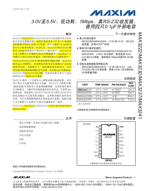
MAX3222/MAX3232/MAX3237/MAX32413.0V至5.5V、低功耗、1Mbps、真RS-232收发器,使用四只0.1µF外部电容________________________________________________________________Maxim Integrated Products119-0273; Rev 7; 1/07MegaBaud和UCSP是Maxim Integrated Products, Inc.的商标。
本文是英文数据资料的译文,文中可能存在翻译上的不准确或错误。
如需进一步确认,请在您的设计中参考英文资料。
有关价格、供货及订购信息,请联络Maxim亚洲销售中心:10800 852 1249 (北中国区),10800 152 1249 (南中国区),或访问Maxim的中文网站:。
M A X 3222/M A X 3232/M A X 3237/M A X 32413.0V至5.5V、低功耗、1Mbps、真RS-232收发器,使用四只0.1µF外部电容2_______________________________________________________________________________________ABSOLUTE MAXIMUM RATINGSELECTRICAL CHARACTERISTICS(V CC = +3.0V to +5.5V, C1–C4 = 0.1µF (Note 2), T A = T MIN to T MAX , unless otherwise noted. Typical values are at T A = +25°C.)Stresses beyond those listed under “Absolute Maximum Ratings” may cause permanent damage to the device. These are stress ratings only, and functional operation of the device at these or any other conditions beyond those indicated in the operational sections of the specifications is not implied. Exposure to absolute maximum rating conditions for extended periods may affect device reliability.Note 1:V+ and V- can have a maximum magnitude of 7V, but their absolute difference cannot exceed 13V.V CC ...........................................................................-0.3V to +6V V+ (Note 1)...............................................................-0.3V to +7V V- (Note 1)................................................................+0.3V to -7V V+ + V- (Note 1)...................................................................+13V Input VoltagesT_IN, SHDN , EN ...................................................-0.3V to +6V MBAUD...................................................-0.3V to (V CC + 0.3V)R_IN.................................................................................±25V Output VoltagesT_OUT...........................................................................±13.2V R_OUT....................................................-0.3V to (V CC + 0.3V)Short-Circuit DurationT_OUT....................................................................ContinuousContinuous Power Dissipation (T A = +70°C)16-Pin TSSOP (derate 6.7mW/°C above +70°C).............533mW 16-Pin Narrow SO (derate 8.70mW/°C above +70°C)....696mW 16-Pin Wide SO (derate 9.52mW/°C above +70°C)........762mW 16-Pin Plastic DIP (derate 10.53mW/°C above +70°C)...842mW 18-Pin SO (derate 9.52mW/°C above +70°C)..............762mW 18-Pin Plastic DIP (derate 11.11mW/°C above +70°C)..889mW 20-Pin SSOP (derate 7.00mW/°C above +70°C).........559mW 20-Pin TSSOP (derate 8.0mW/°C above +70°C).............640mW 28-Pin TSSOP (derate 8.7mW/°C above +70°C).............696mW 28-Pin SSOP (derate 9.52mW/°C above +70°C).........762mW 28-Pin SO (derate 12.50mW/°C above +70°C).....................1W Operating Temperature RangesMAX32_ _C_ _.....................................................0°C to +70°C MAX32_ _E_ _ .................................................-40°C to +85°C Storage Temperature Range.............................-65°C to +150°C Lead Temperature (soldering, 10s).................................+300°CMAX3222/MAX3232/MAX3237/MAX32413.0V至5.5V、低功耗、1Mbps、真RS-232收发器,使用四只0.1µF外部电容_______________________________________________________________________________________3TIMING CHARACTERISTICS—MAX3222/MAX3232/MAX3241(V CC = +3.0V to +5.5V, C1–C4 = 0.1µF (Note 2), T A = T MIN to T MAX , unless otherwise noted. Typical values are at T A = +25°C.)ELECTRICAL CHARACTERISTICS (continued)(V CC = +3.0V to +5.5V, C1–C4 = 0.1µF (Note 2), T A = T MIN to T MAX , unless otherwise noted. Typical values are at T A = +25°C.)A X 3222/M A X 3232/M A X 3237/M A X 32413.0V至5.5V、低功耗、1Mbps、真RS-232收发器,使用四只0.1µF外部电容4_______________________________________________________________________________________典型工作特性Ω, T A = +25°C, unless otherwise noted.)LOAD CAPACITANCE (pF)0246810121416182022150MAX3222/MAX3232SLEW RATEvs. LOAD CAPACITANCELOAD CAPACITANCE (pF)S L E W R A T E (V /µs )20003000100040005000510152025303540MAX3222/MAX3232SUPPLY CURRENT vs. LOAD CAPACITANCEWHEN TRANSMITTING DATALOAD CAPACITANCE (pF)S U P P L Y C U R R E N T (m A )20003000100040005000TIMING CHARACTERISTICS—MAX3237(V CC = +3.0V to +5.5V, C1–C4 = 0.1µF (Note 2), T A = T MIN to T MAX , unless otherwise noted. Typical values are at T A = +25°C.)Note 2:MAX3222/MAX3232/MAX3241: C1–C4 = 0.1µF tested at 3.3V ±10%; C1 = 0.047µF, C2–C4 = 0.33µF tested at 5.0V ±10%.MAX3237: C1–C4 = 0.1µF tested at 3.3V ±5%; C1–C4 = 0.22µF tested at 3.3V ±10%; C1 = 0.047µF, C2–C4 = 0.33µF tested at 5.0V ±10%.Note 3:Transmitter input hysteresis is typically 250mV.MAX3222/MAX3232/MAX3237/MAX32413.0V至5.5V、低功耗、1Mbps、真RS-232收发器,使用四只0.1µF外部电容_______________________________________________________________________________________5-7.5-5.0-2.502.55.07.50MAX3241TRANSMITTER OUTPUT VOLTAGEvs. LOAD CAPACITANCELOAD CAPACITANCE (pF)T R A N S M I T T E R O U T P U T V O L T A G E (V )2000300010004000500046810121416182022240MAX3241SLEW RATEvs. LOAD CAPACITANCELOAD CAPACITANCE (pF)S L E W R A T E (V /µs )20003000100040005000510152025303545400MAX3241SUPPLY CURRENT vs. LOADCAPACITANCE WHEN TRANSMITTING DATALOAD CAPACITANCE (pF)S U P P L Y C U R R E N T (m A )20003000100040005000-7.5-5.0-2.502.55.07.50MAX3237TRANSMITTER OUTPUT VOLTAGE vs. LOAD CAPACITANCE (MBAUD = GND)LOAD CAPACITANCE (pF)T R A N S M I T T E R O U T P U T V O L T A G E (V )200030001000400050000102030504060700MAX3237SLEW RATE vs. LOAD CAPACITANCE(MBAUD = V CC )LOAD CAPACITANCE (pF)S L E W R A T E (V /µs )500100015002000-7.5-5.0-2.502.55.07.50MAX3237TRANSMITTER OUTPUT VOLTAGE vs. LOAD CAPACITANCE (MBAUD = V CC )LOAD CAPACITANCE (pF)T R A N S M I T T E R O U T P U T V O L T A G E (V )5001000150020001020304050600MAX3237SUPPLY CURRENT vs.LOAD CAPACITANCE (MBAUD = GND)LOAD CAPACITANCE (pF)S U P P L Y C U R R E N T (m A )200030001000400050000246810120MAX3237SLEW RATE vs. LOAD CAPACITANCE(MBAUD = GND)LOAD CAPACITANCE (pF)S L E W R A T E (V /µs )2000300010004000500010302040506070MAX3237SKEW vs. LOAD CAPACITANCE(t PLH - t PHL )LOAD CAPACITANCE (pF)1000150050020002500____________________________________________________________________典型工作特性(续)(V CC = +3.3V, 235kbps data rate, 0.1µF capacitors, all transmitters loaded with 3k Ω, T A = +25°C, unless otherwise noted.)M A X 3222/M A X 3232/M A X 3237/M A X 32413.0V至5.5V、低功耗、1Mbps、真RS-232收发器,使用四只0.1µF外部电容6_________________________________________________________________________________________________________________________________________________________________引脚说明MAX3222/MAX3232/MAX3237/MAX32413.0V至5.5V、低功耗、1Mbps、真RS-232收发器,使用四只0.1µF外部电容_______________________________________________________________________________________7_______________________________详细说明双电荷泵电压转换器MAX3222/MAX3232/MAX3237/MAX3241的内部电源由两路稳压型电荷泵组成,只要输入电压(V CC )在3.0V至5.5V范围以内,即可提供+5.5V (倍压电荷泵)和-5.5V (反相电荷泵)输出电压。
MAX882中文资料
19-0275; Rev 0; 12/94
5V/3.3V or Adjustable, Low-Dropout, Low IQ, 200mA Linear Regulators
_______________General Description
The MAX882/MAX883/MAX884 linear regulators maximize battery life by combining ultra-low supply currents and low dropout voltages. They feature 200mA output current capability at up to +125°C junction temperature and come in a 1.5W SOIC package. The 1.5W package (compared to 0.47W for standard SOIC packages) allows a wider operating range for the input voltage and output current. The MAX882/MAX883/MAX884 use a Pchannel MOSFET pass transistor to maintain a low 11µA (15µA max) supply current from no-load to the full 200mA output. Unlike earlier bipolar regulators, there are no PNP base current losses that increase with output current. And, in dropout, the MOSFET does not suffer from excessive base currents that occur when PNP transistors go into saturation. Typical dropout voltages are 220mV at 5V and 200mA, or 320mV at 3.3V and 200mA. The MAX882 features a 7µA standby mode that disables the output but keeps the reference, low-battery comparator, and biasing circuitry alive. The MAX883/MAX884 feature a shutdown (OFF) mode that turns off all circuitry, reducing supply current to less than 1µA. All three devices include a low-battery-detection comparator, foldback current limiting, reverse-current protection, and thermal overload protection. The output is preset at 3.3V for the MAX882/MAX884 and 5V for the MAX883. In addition, all devices employ Dual Mode™ operation, allowing user-adjustable outputs from 1.25V to 11V using external resistors. The input voltage supply range is 2.7V to 11.5V. For low-dropout linear regulators with output currents up to 500mA, refer to the MAX603/MAX604 data sheet.
MAXIM 化数字电位器MAX5481, MAX5482, MAX5483, MAX548 说明书

ENGLISH•简体中文•日本語•概述状况状况:生产中。
下载Notes MAX5481Linear13-WireSerial SPINon-Volatile102410253519.6$1.95@1kMAX548250$1.95 @1kMAX548310$1.95 @1kMAX548450$1.95 @1k查看所有Digital Potentiometers (128)引脚配置相关产品MAX5494,MAX5495,MAX5496, ...10位、双路、非易失、线性变化数字电位器类似产品:浏览其它类似产品线查看所有Digital Potentiometers (128产品)顶标MAX5481顶标MAX5482顶标MAX5483顶标MAX5484新品发布[ 2005-08-03 ]应用工程师帮助选型,下个工作日回复参数搜索应用帮助概述技术文档定购信息概述关键特性应用/使用关键指标图表注释、注解相关产品数据资料应用笔记评估板设计指南可靠性报告软件/模型价格与供货样品在线订购封装信息无铅信息参考文献: 19-3708 Rev. 4; 2008-03-12本页最后一次更新: 2008-03-27联络我们:信息反馈、提出问题 • 对该网页的评价 • 发送本网页 • 隐私权政策 • 法律声明 © 2010 Maxim Integrated Products版权所有General DescriptionThe MAX5481–MAX5484 10-bit (1024-tap) nonvolatile,linear-taper, programmable voltage-dividers and vari-able resistors perform the function of a mechanical potentiometer, but replace the mechanics with a pin-configurable 3-wire serial SPI™-compatible interface or up/down digital interface. The MAX5481/MAX5482 are 3-terminal voltage-dividers and the MAX5483/MAX5484are 2-terminal variable resistors.The MAX5481–MAX5484 feature an internal, non-volatile, electrically erasable programmable read-only memory (EEPROM) that stores the wiper position for ini-tialization during power-up. The 3-wire SPI-compatible serial interface allows communication at data rates up to 7MHz. A pin-selectable up/down digital interface is also available.The MAX5481–MAX5484 are ideal for applications requiring digitally controlled potentiometers. Two end-to-end resistance values are available (10k Ωand 50k Ω) in a voltage-divider or a variable-resistor configuration (see the Selector G uide ). The nominal resistor temperature coefficient is 35ppm/°C end-to-end, and only 5ppm/°C ratiometric, making these devices ideal for applications requiring low-temperature-coefficient voltage-dividers,such as low-drift, programmable gain-amplifiers.The MAX5481–MAX5484 operate with either a +2.7V to +5.25V single power supply or ±2.5V dual power sup-plies. These devices consume 400µA (max) of supply current when writing data to the nonvolatile memory and 1.0µA (max) of standby supply current. The MAX5481–MAX5484 are available in a space-saving (3mm x 3mm), 16-pin TQFN, or a 14-pin TSSOP pack-age and are specified over the extended (-40°C to +85°C) temperature range.ApplicationsFeatures♦1024 Tap Positions♦Power-On Recall of Wiper Position from Nonvolatile Memory♦16-Pin (3mm x 3mm x 0.8mm) TQFN or 14-Pin TSSOP Package♦35ppm/°C End-to-End Resistance Temperature Coefficient♦5ppm/°C Ratiometric Temperature Coefficient ♦10kΩand 50kΩEnd-to-End Resistor Values♦Pin-Selectable SPI-Compatible Serial Interface or Up/Down Digital Interface ♦1µA (max) Standby Current♦Single +2.7V to +5.25V Supply Operation ♦Dual ±2.5V Supply OperationMAX5481–MAX548410-Bit, Nonvolatile, Linear-Taper DigitalPotentiometers________________________________________________________________Maxim Integrated Products1Ordering InformationPin Configurations19-3708; Rev 5; 4/10For pricing delivery, and ordering information please contact Maxim Direct at 1-888-629-4642,or visit Maxim’s website at .Selector Guide appears at end of data sheet.SPI is a trademark of Motorola, Inc.temperature range.+Denotes a lead(Pb)-free/RoHS-compliant package.*EP = Exposed pad.Ordering Information continued at end of data sheet.Gain and Offset AdjustmentLCD Contrast Adjustment Pressure SensorsLow-Drift Programmable Gain AmplifiersMechanical Potentiometer ReplacementM A X 5481–M A X 548410-Bit, Nonvolatile, Linear-Taper Digital PotentiometersABSOLUTE MAXIMUM RATINGSStresses beyond those listed under “Absolute Maximum Ratings” may cause permanent damage to the device. These are stress ratings only, and functional operation of the device at these or any other conditions beyond those indicated in the operational sections of the specifications is not implied. Exposure to absolute maximum rating conditions for extended periods may affect device reliability.V DD to GND...........................................................-0.3V to +6.0V V SS to GND............................................................-3.5V to +0.3V V DD to V SS .............................................................-0.3V to +6.0V H, L, W to V SS ..................................(V SS - 0.3V) to (V DD + 0.3V)CS , SCLK(INC ), DIN(U/D ), SPI/UD to GND..-0.3V to (V DD + 0.3V)Maximum Continuous Current into H, L, and WMAX5481/MAX5483.........................................................±5mA MAX5482/MAX5484......................................................±1.0mA Maximum Current into Any Other Pin...............................±50mAContinuous Power Dissipation (T A = +70°C)16-Pin TQFN (derate 17.5mW/°C above +70°C).....1398.6mW 14-Pin TSSOP (derate 9.1mW/°C above +70°C)..........727mW Operating Temperature Range ...........................-40°C to +85°C Junction Temperature......................................................+150°C Storage Temperature Range.............................-60°C to +150°C Lead Temperature (soldering, 10s).................................+300°C Soldering Temperature (reflow).......................................+260°CELECTRICAL CHARACTERISTICSMAX5481–MAX548410-Bit, Nonvolatile, Linear-Taper DigitalPotentiometers_______________________________________________________________________________________3ELECTRICAL CHARACTERISTICS (continued)(V DD = +2.7V to +5.25V, V SS = V GND = 0V, V H = V DD , V L = 0V, T A = -40°C to +85°C, unless otherwise noted. Typical values are at V DD = +5.0V, T A = +25°C, unless otherwise noted.) (Note 1)M A X 5481–M A X 548410-Bit, Nonvolatile, Linear-Taper Digital Potentiometers 4_______________________________________________________________________________________TIMING CHARACTERISTICSNote 2:The DNL and INL are measured with the device configured as a voltage-divider with H = V DD and L = V SS . The wiper termi-nal (W) is unloaded and measured with a high-input-impedance voltmeter.Note 3:The DNL_R and INL_R are measured with D.N.C. unconnected and L = V SS = 0V. For V DD = +5V, the wiper terminal is dri-ven with a source current of I W = 80µA for the 50k Ωdevice and 400µA for the 10k Ωdevice. For V DD = +3V, the wiper termi-nal is driven with a source current of 40µA for the 50k Ωdevice and 200µA for the 10k Ωdevice.Note 4:The wiper resistance is measured using the source currents given in Note 3.Note 5:The device draws higher supply current when the digital inputs are driven with voltages between (V DD - 0.5V) and (V GND +0.5V). See Supply Current vs. Digital Input Voltage in the Typical Operating Characteristics .Note 6:Wiper settling test condition uses the voltage-divider configuration with a 10pF load on W. Transition code from 00000 00000to 01111 01111 and measure the time from CS going high to the wiper voltage settling to within 0.5% of its final value.MAX5481–MAX548410-Bit, Nonvolatile, Linear-Taper DigitalPotentiometers_______________________________________________________________________________________5-1.0-0.6-0.8-0.2-0.40.200.40.80.61.002563841285126407688961024DNL vs. CODE (MAX5483)CODED N L (L S B )V DD = 2.7V-1.0-0.6-0.8-0.2-0.40.200.40.80.61.002563841285126407688961024DNL vs. CODE (MAX5483)CODED N L (L S B )V DD = 5V-2.0-1.0-1.50-0.50.51.01.5 2.0INL vs. CODE (MAX5483)I N L (L S B )V DD = 2.7V02563841285126407688961024CODE-2.0-1.0-1.50-0.50.51.01.5 2.0INL vs. CODE (MAX5483)I N L (L S B )V DD = 3V2563841285126407688961024CODE-2.0-1.0-1.50-0.50.51.01.5 2.0INL vs. CODE (MAX5483)I N L (L S B )V DD = 5V02563841285126407688961024CODE-1.0-0.6-0.8-0.2-0.40.200.40.80.61.002563841285126407688961024DNL vs. CODE (MAX5481)CODED N L (L S B )-1.0-0.6-0.8-0.2-0.40.200.40.80.61.002563841285126407688961024DNL vs. CODE (MAX5481)CODED N L (L S B )V DD = 5V-1.0-0.6-0.8-0.2-0.40.200.40.80.61.002563841285126407688961024INL vs. CODE (MAX5481)CODEI N L (L S B )-1.0-0.6-0.8-0.2-0.40.200.40.80.61.002563841285126407688961024INL vs. CODE (MAX5481)CODEI N L (L S B )Typical Operating Characteristics(V DD = 5.0V, V SS = 0V, T A = +25°C, unless otherwise noted.)M A X 5481–M A X 548410-Bit, Nonvolatile, Linear-Taper Digital Potentiometers 6_______________________________________________________________________________________-1.0-0.6-0.8-0.2-0.40.200.40.80.61.002563841285126407688961024DNL vs. CODE (MAX5484)CODED N L (L S B )-1.0-0.6-0.8-0.2-0.40.200.40.80.61.002563841285126407688961024DNL vs. CODE (MAX5484)CODED N L (L S B )-1.0-0.6-0.8-0.2-0.40.200.40.80.61.002563841285126407688961024INL vs. CODE (MAX5484)CODEI N L (L S B )-1.0-0.6-0.8-0.2-0.40.200.40.80.61.002563841285126407688961024INL vs. CODE (MAX5484)CODEI N L (L S B )-1.0-0.6-0.8-0.2-0.40.200.40.80.61.002563841285126407688961024DNL vs. CODE (MAX5482)CODED N L (L S B )-1.0-0.6-0.8-0.2-0.40.200.40.80.61.002563841285126407688961024DNL vs. CODE (MAX5482)CODED N L (L S B )-1.0-0.6-0.8-0.2-0.40.200.40.80.61.002563841285126407688961024INL vs. CODE (MAX5482)CODEI N L (L S B )V DD = 2.7V-1.0-0.6-0.8-0.2-0.40.200.40.80.61.02563841285126407688961024INL vs. CODE (MAX5482)CODEI N L (L S B )V DD = 5V02010403050607080WIPER RESISTANCE vs. CODE (VARIABLE RESISTOR, T A = -40°C)M A X 5481 t o c 18R W (Ω)2563841285126407688961024CODETypical Operating Characteristics (continued)(V DD = 5.0V, V SS = 0V, T A = +25°C, unless otherwise noted.)MAX5481–MAX5484Typical Operating Characteristics (continued)(V DD = 5.0V, V SS = 0V, T A = +25°C, unless otherwise noted.)10-Bit, Nonvolatile, Linear-Taper DigitalPotentiometers_______________________________________________________________________________________702010403050607080WIPER RESISTANCE vs. CODE (VARIABLE RESISTOR, T A = +25°C)M A X 5481 t oc 19R W (Ω)2563841285126407688961024CODE2010403050607080WIPER RESISTANCE vs. CODE (VARIABLE RESISTOR, T A = +85°C)M A X 5481 t o c 20R W (Ω)2563841285126407688961024CODE10302050604070W-TO-L RESISTANCE vs. CODE(MAX5484)R W L (k Ω)02563841285126407688961024CODE02641012814W-TO-L RESISTANCE vs. CODE(MAX5483)R W L (k Ω)2563841285126407688961024CODE18.018.519.019.520.020.521.021.522.0012345WIPER RESISTANCE vs. WIPER VOLTAGE(VARIABLE RESISTOR)WIPER VOLTAGE (V)R W (Ω)-2.0-1.5-1.0-0.500.51.01.52.0-40-1510356085END-TO-END (R HL ) % CHANGE vs. TEMPERATURE (VOLTAGE-DIVIDER)M A X 5481 t o c 24TEMPERATURE (°C)E N D -T O -E N D R E S I S T A N C E C H A N G E (%)-2.0-1.5-1.0-0.500.51.01.52.0-40-1510356085WIPER-TO-END RESISTANCE (R WL ) % CHANGE vs. TEMPERATURE (VARIABLE RESISTOR)TEMPERATURE (°C)W I P E R -T O -E N D R E S I S T A N C E C H A N G E (%)00.30.90.61.21.5-4010-15356085STANDBY SUPPLY CURRENTvs. TEMPERATURETEMPERATURE (°C)I D D (μA )DIGITAL SUPPLY CURRENT vs. DIGITAL INPUT VOLTAGEDIGITAL INPUT VOLTAGE (V)I D D (μA )4.54.03.53.02.52.01.51.00.5110100100010,0000.15.0M A X 5481–M A X 548410-Bit, Nonvolatile, Linear-Taper Digital Potentiometers Typical Operating Characteristics (continued)(Circuit of Figure 1, T A = +25°C, unless otherwise noted.)1μs/divTAP-TO-TAP SWITCHING TRANSIENTRESPONSE (MAX5481)V W(AC-COUPLED)20mV/divCS 2V/divH = V DD , L = GND C W = 10pFFROM CODE 01 1111 1111TO CODE 10 0000 00004μs/divTAP-TO-TAP SWITCHING TRANSIENTRESPONSE (MAX5482)V W(AC-COUPLED)20mV/divCS 2V/divH = V DD , L = GND C W = 10pFFROM CODE 01 1111 1111TO CODE 10 0000 0000WIPER RESPONSE vs. FREQUENCY(MAX5481)FREQUENCY (kHz)G A I N (d B )100101-20-15-10-5-250.11000WIPER RESPONSE vs. FREQUENCY(MAX5482)FREQUENCY (kHz)G A I N (d B )100101-20-15-10-50-250.11000THD+N vs. FREQUENCY(MAX5481)FREQUENCY (kHz)T H D +N (%)1010.10.0010.010.11100.00010.01100THD+N vs. FREQUENCY(MAX5482)FREQUENCY (kHz)T H D +N (%)1010.10.0010.010.11100.00010.0110004020806012010014018016020002563841285126407688961024RATIOMETRIC TEMPERATURE COEFFICIENT vs. CODECODER A T I O M E T R I C T E M P C O (p p m )100300200500600400700VARIABLE-RESISTOR TEMPERATURECOEFFICIENT vs. CODET C V R (p p m )02563841285126407688961024CODE10-Bit, Nonvolatile, Linear-Taper DigitalPotentiometersPin DescriptionMAX5481–MAX5484M A X 5481–M A X 548410-Bit, Nonvolatile, Linear-Taper Digital Potentiometers Pin Description (continued)(MAX5483/MAX5484 Variable Resistors)MAX5481–MAX548410-Bit, Nonvolatile, Linear-Taper DigitalPotentiometersFunctional DiagramsM A X 5481–M A X 548410-Bit, Nonvolatile, Linear-Taper Digital Potentiometers Detailed DescriptionThe MAX5481/MAX5482 linear programmable voltage-dividers and the MAX5483/MAX5484 variable resistors feature 1024 tap points (10-bit resolution) (see the Functional Diagrams ). These devices consist of multi-ple strings of equal resistor segments with a wiper con-tact that moves among the 1024 points through a pin-selectable 3-wire SPI-compatible serial interface or up/down interface. The MAX5481/MAX5483 provide a total end-to-end resistance of 10k Ω, and the MAX5482/MAX5484 have an end-to-end resistance of 50k Ω. The MAX5481/MAX5482 allow access to the high, low, and wiper terminals for a standard voltage-divider configuration.MAX5481/MAX5482 ProgrammableVoltage-DividersThe MAX5481/MAX5482 programmable voltage-dividers provide a weighted average of the voltage between the H and L inputs at the W output. Both devices feature 10-bit resolution and provide up to 1024 tap points between the H and L voltages. Ideally,the V L voltage occurs at the wiper terminal (W) when all data bits are zero and the V H voltage occurs at the wiper terminal when all data bits are one. The step size (1 LSB) voltage is equal to the voltage applied across terminals H and L divided by 210. Calculate the wiper voltage V Was follows:Functional Diagrams (continued)MAX5481–MAX548410-Bit, Nonvolatile, Linear-Taper DigitalPotentiometerswhere D is the decimal equivalent of the 10 data bits writ-ten (0 to 1023), V HL is the voltage difference between the H and L terminals:The MAX5481 includes a total end-to-end resistance value of 10k Ωwhile the MAX5482 features an end-to-end resistance value of 50k Ω. These devices are not intended to be used as a variable resistor . Wiper cur-rent creates a nonlinear voltage drop in series with the wiper. To ensure temperature drift remains within speci-fications, do not pull current through the voltage-divider wiper. Connect the wiper to a high-impedance node.Figures 1 and 2 show the behavior of the MAX5481’s resistance from W to H and from W to L. This does not apply to the variable-resistor devicesMAX5483/MAX5484 Variable ResistorsThe MAX5483/MAX5484 provide a programmable resistance between W and L. The MAX5483 features a total end-to-end resistance value of 10k Ω, while the MAX5484 provides an end-to-end resistance value of 50k Ω. The programmable resolution of this resistance is equal to the nominal end-to-end resistance divided by 1024 (10-bit resolution). For example, each nominal segment resistance is 9.8Ωand 48.8Ωfor the MAX5483and the MAX5484, respectively.wiper position from the 1024 possible positions, result-ing in 1024 values for the resistance from W to L.Calculate the resistance from W to L (R WL ) by using the where D is decimal equivalent of the 10 data bits writ-ten, R W-L is the nominal end-to-end resistance, and R Z is the zero-scale error. Table 1 shows the values of R WL at selected codes for the MAX5483/MAX5484.Digital InterfaceConfigure the MAX5481–MAX5484 by a pin-selectable,3-wire, SPI-compatible serial data interface or an up/down interface. Drive SPI/UD high to select the 3-wire SPI-compatible interface. Pull SPI/UD low to select the up/down interface.V FSE V andV ZSE V FSE HL ZSE HL =⎡⎣⎢⎤⎦⎥=⎡⎣⎢⎤⎦⎥10241024,Figure 1. Resistance from W to H vs. Code (10k ΩVoltage-Divider)Figure 2. Resistance from W to L vs. Code (10k ΩVoltage-Divider)M A X 5481–M A X 548410-Bit, Nonvolatile, Linear-Taper Digital Potentiometers SPI-Compatible Serial InterfaceDrive SPI/UD high to enable the 3-wire SPI-compatible serial interface (see Figure 3). This write-only interface contains three inputs: chip select (CS ), data in (DIN(U/D )), and data clock (SCLK(INC )). Drive CS low to load the data at DIN(U/D ) synchronously into the shift register on each SCLK(INC ) rising edge.The WRITE command (C1, C0 = 00) requires 24 clock cycles to transfer the command and data (Figure 4a).The COPY commands (C1, C0 = 10 or 11) use either eight clock cycles to transfer the command bits (Figure 4b) or 24 clock cycles with the last 16 data bits disre-garded by the device.After loading the data into the shift register, drive CS high to latch the data into the appropriate control regis-ter. Keep CS low during the entire serial data stream to avoid corruption of the data. Table 2 shows the com-mand decoding.Write Wiper RegisterData written to this register (C1, C0 = 00) controls the wiper position. The 10 data bits (D9–D0) indicate the position of the wiper. For example, if DIN(U/D ) = 00 00000000, the wiper moves to the position closest to L. If DIN(U/D ) = 11 1111 1111, the wiper moves closest to H.This command writes data to the volatile random access memory (RAM), leaving the NV register unchanged. When the device powers up, the data stored in the NV register transfers to the wiper register,moving the wiper to the stored position. Figure 5 shows how to write data to the wiper register.Table 2. Command Decoding*X = Don’t care.Figure 3. SPI-Compatible Serial-Interface Timing Diagram (SPI/UD = 1)10-Bit, Nonvolatile, Linear-Taper DigitalPotentiometers ArrayMAX5481–MAX5484Figure4. Serial SPI-Compatible Interface FormatFigure5. Write Wiper Register OperationM A X 5481–M A X 548410-Bit, Nonvolatile, Linear-Taper Digital Potentiometers Copy Wiper Register to NV RegisterThe copy wiper register to NV register command (C1,C0 = 10) stores the current position of the wiper to the NV register for use at power-up. Figure 6 shows how to copy data from wiper register to NV register. The oper-ation takes up to 12ms (max) after CS goes high to complete and no other operation should be performed until completion.Copy NV Register to Wiper RegisterThe copy NV register to wiper register (C1, C0 = 11)restores the wiper position to the current value stored in the NV register. Figure 7 shows how to copy data from the NV register to the wiper register.Digital Up/Down InterfaceFigure 8 illustrates an up/down serial-interface timing diagram. In digital up/down interface mode (SPI/UD =0), the logic inputs CS , DIN(U/D ), and SCLK(INC ) con-trol the wiper position and store it in nonvolatile memory (see Table 3). The chip-select (CS ) input enables the serial interface when low and disables the interface when high. The position of the wiper is stored in the nonvolatile register when CS transitions from low to high while SCLK(INC ) is high.When the serial interface is active (CS low), a high-to-low (falling edge) transition on SCLK(INC ) increments or decrements the internal 10-bit counter depending on the state of DIN(U/D ). If DIN(U/D ) is high, the wiper increments. If DIN(U/D ) is low, the wiper decrements.The device stores the value of the wiper position in the nonvolatile memory when CS transitions from low to high while SCLK(INC ) is high. The host system can disablethe serial interface and deselect the device without stor-ing the latest wiper position in the nonvolatile memory by keeping SCLK(INC ) low while taking CS high.Upon power-up, the MAX5481–MAX5484 load the value of nonvolatile memory into the wiper register, and set the wiper position to the value last stored.Figure 6. Copy Wiper Register to NV Register OperationFigure 7. Copy NV Register to Wiper Register OperationMAX5481–MAX548410-Bit, Nonvolatile, Linear-Taper DigitalPotentiometersStandby ModeThe MAX5481–MAX5484 feature a low-power standby mode. When the device is not being programmed, it enters into standby mode and supply current drops to 0.5µA (typ).Nonvolatile MemoryThe internal EEPROM consists of a nonvolatile register that retains the last value stored prior to power-down.The nonvolatile register is programmed to midscale at the factory. The nonvolatile memory is guaranteed for 50 years of wiper data retention and up to 200,000wiper write cycles.Power-UpUpon power-up, the MAX5481–MAX5484 load the data stored in the nonvolatile wiper register into the volatile wiper register, updating the wiper position with the data stored in the nonvolatile wiper register.Applications InformationThe MAX5481–MAX5484 are ideal for circuits requiring digitally controlled adjustable resistance, such as LCD contrast control (where voltage biasing adjusts the dis-play contrast), or programmable filters with adjustable gain and/or cutoff frequency.Positive LCD Bias ControlFigures 9 and 10 show an application where a voltage-divider or a variable resistor is used to make an adjustable, positive LCD-bias voltage. The op amp pro-vides buffering and gain to the voltage-divider network made by the programmable voltage-divider (Figure 9) or to a fixed resistor and a variable resistor (see Figure 10).Programmable Gain and Offset AdjustmentFigure 11 shows an application where a voltage-divider and a variable resistor are used to make a programma-ble gain and offset adjustment.Figure 8. Up/Down Serial-Interface Timing Diagram (SPI/UD = 0)M A X 5481–M A X 548410-Bit, Nonvolatile, Linear-Taper Digital Potentiometers 18______________________________________________________________________________________Programmable FilterFigure 12 shows the configuration for a 1st-order pro-grammable filter using two variable resistors. Adjust R2for the gain and adjust R3 for the cutoff frequency. Use the following equations to estimate the gain (G) and the 3dB cutoff frequency (f C):Figure 10. Positive LCD Bias Control Using a Variable ResistorFigure 12. Programmable FilterFigure 11. Programmable Gain/Offset AdjustmentFigure 9. Positive LCD Bias Control Using a Voltage-DividerMAX5481–MAX548410-Bit, Nonvolatile, Linear-Taper DigitalPotentiometers______________________________________________________________________________________19Chip InformationPROCESS: BiCMOSSelector GuidePin Configurations (continued)Ordering Information (continued)Note: All devices are specified over the -40°C to +85°C operating temperature range.+Denotes a lead(Pb)-free/RoHS-compliant package.*EP = Exposed pad.Package InformationFor the latest package outline information and land patterns, go to /packages . Note that a “+”, “#”, or “-” in the package code indicates RoHS status only. Package draw-ings may show a different suffix character, but the drawing per-tains to the package regardless of RoHS status.M A X 5481–M A X 548410-Bit, Nonvolatile, Linear-Taper Digital Potentiometers Maxim cannot assume responsibility for use of any circuitry other than circuitry entirely embodied in a Maxim product. No circuit patent licenses are implied. Maxim reserves the right to change the circuitry and specifications without notice at any time.20____________________Maxim Integrated Products, 120 San Gabriel Drive, Sunnyvale, CA 94086 408-737-7600©2010 Maxim Integrated ProductsMaxim is a registered trademark of Maxim Integrated Products, Inc.。
MAX320-MAX322中文资料
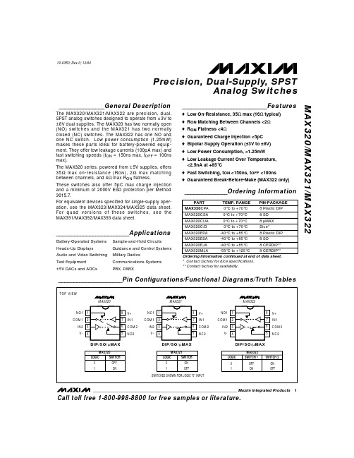
ELECTRICAL CHARACTERISTICS
(V+ = +5V ±10%, V- = -5V ±10%, VINH = 3.5V, VINL = 2.5V, TA = TMIN to TMAX, unless otherwise noted.)
PARAMETER ANALOG SWITCH Analog Signal Range
For equivalent devices specified for single-supply operation, see the MAX323/MAX324/MAX325 data sheet. For quad versions of these switches, see the MAX391/MAX392/MAX393 data sheet.
Plastic DIP (derate 9.09mW/°C above +70°C) .............727mW Narrow SO (derate 5.88mW/°C above +70°C) .............471mW
µMAX (derate 4.10mW/°C above +70°C) .....................330mW CERDIP (derate 8.00mW/°C above +70°C) ..................640mW Operating Temperature Ranges MAX32_C_ _ ........................................................0°C to +70°C MAX32_E_ _......................................................-40°C to +85°C MAX32_MJA ...................................................-55°C to +125°C Storage Temperature Range .............................-65°C to +150°C Lead Temperature (soldering, 10sec) .............................+300°C
OMAPL138硬件说明

1. 开发板简介YXDSP-OMAPL138至尊板是南京研旭电气科技有限公司特针对高校、研究所和中小企业的设计需求而自主研发的产品。
该开发板可以满足基于OMAPL138开发时的所有应用,板卡提供了丰富的二次开发接口,能够为您基于OMAPL138的设计节约成本和时间。
目前,我们的产品已经广泛应用于众多科研院所、高校、电力电子类、通讯类、工业类、医疗类公司,在长期的客户产品开发使用过程中得到高度认可和好评。
YXDSP-OMAPL138至尊板采用了核心板+功能底板合并分拆的结构,在保证DSP能稳定独立运行、外设资源充分扩展的基础上,优化结构设计,注重EMC处理。
核心板采用6层PCB设计,功能底板采用2层PCB设计。
产品的抗电磁干扰能力性能优越,可将产品用于工业现场。
TI公司的达芬奇架构嵌入式应用处理器开始使用DSP与ARM结合的非对称多核结构。
OMAPL138就是其中的一款低功耗双核嵌入式处理器。
OMAPL138双核构架兼具DSP内核和ARM926EJ-S内核。
ARM926EJ-S是一个执行32位、16位指令和处理32位、16位或8位数据的32为RISC 处理器内核。
该内核采用流水线的结构,因此处理器和储存器系统的所有部件都可连续地工作。
ARM内核有一个协处理器15(CP15)、保护模块、数据和程序储存器管理单元(MMUs)以及后备缓冲器。
它具有分离的16KB的指令高速缓存和16KB的数据高速缓存。
两者通过虚拟索引虚拟标签形成四路关联。
另外,ARM内核还具有一个8KB的RAM(矢量表)和64KB 的ROM。
DSP核采用了一个2级基于高速缓存的架构。
Level1程序高速缓存(L1P)是一个32KB 直接映射的高速缓存,Level1数据高速缓存(L1D)是一个32KB的两路组关联高速缓存。
Level2程序高速缓存(L2P)包含256KB的内存空间,为程序空间和数据包空间所共享。
L2配置为映射内存、高速缓存或者两者的结合。
MAX3087ESA中文资料
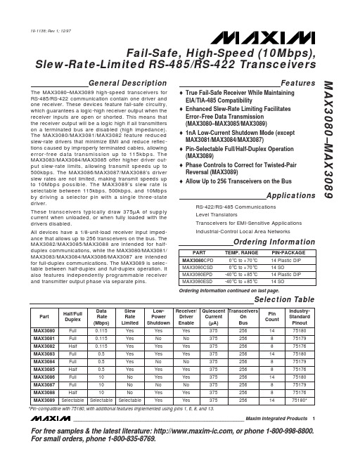
375
256
MAX3084
Full
0.5
Yes
No
No
375
256
MAX3085
Half
0.5
Yes
Yes
Yes
375
256
MAX3086
Full
10
No
Yes
Yes
375
256
MAX3087
Full
10
No
No
No
375
256
MAX3088
Half
10
No
Yes
Yes
375
256
MAX3089 Selectable Selectable Selectable
These transceivers typically draw 375µA of supply current when unloaded, or when fully loaded with the drivers disabled.
All devices have a 1/8-unit-load receiver input impedance that allows up to 256 transceivers on the bus. The MAX3082/MAX3085/MAX3088 are intended for halfduplex communications, while the MAX3080/MAX3081/ MAX3083/MAX3084/MAX3086/MAX3087 are intended for full-duplex communications. The MAX3089 is selectable between half-duplex and full-duplex operation. It also features independently programmable receiver and transmitter output phase via separate pins.
MAX630CSA+中文资料
General DescriptionMaxim’s MAX630 and MAX4193 CMOS DC-DC regula-tors are designed for simple, efficient, minimum-size DC-DC converter circuits in the 5mW to 5W range. The MAX630 and MAX4193 provide all control and power handling functions in a compact 8-pin package: a 1.31V bandgap reference, an oscillator, a voltage com-parator, and a 375mA N-channel output MOSF ET. A comparator is also provided for low-battery detection.Operating current is only 70µA and is nearly indepen-dent of output switch current or duty cycle. A logic-level input shuts down the regulator to less than 1µA quies-cent current. Low-current operation ensures high effi-ciency even in low-power battery-operated systems.The MAX630 and MAX4193 are compatible with most battery voltages, operating from 2.0V to 16.5V.The devices are pin compatible with the Raytheon bipo-lar circuits, RC4191/2/3, while providing significantly improved efficiency and low-voltage operation. Maxim also manufactures the MAX631, MAX632, and MAX633DC-DC converters, which reduce the external compo-nent count in fixed-output 5V, 12V, and 15V circuits.See Table 2 at the end of this data sheet for a summary of other Maxim DC-DC converters.Applications+5V to +15V DC-DC ConvertersHigh-Efficiency Battery-Powered DC-DC Converters+3V to +5V DC-DC Converters 9V Battery Life ExtensionUninterruptible 5V Power Supplies5mW to 5W Switch-Mode Power SuppliesFeatures♦High Efficiency—85% (typ)♦70µA Typical Operating Current ♦1µA Maximum Quiescent Current ♦2.0V to 16.5V Operation♦525mA (Peak) Onboard Drive Capability ♦±1.5% Output Voltage Accuracy (MAX630)♦Low-Battery Detector♦Compact 8-Pin Mini-DIP and SO Packages ♦Pin Compatible with RC4191/2/3MAX630/MAX4193CMOS Micropower Step-UpSwitching Regulator________________________________________________________________Maxim Integrated Products 1Pin ConfigurationOrdering InformationTypical Operating Circuit19-0915; Rev 2; 9/08For pricing, delivery, and ordering information,please contact Maxim/Dallas Direct!at 1-888-629-4642, or visit Maxim’s website at .*Dice are specified at T A = +25°C. Contact factory for dice specifications.**Contact factory for availability and processing to MIL-STD-883.†Contact factory for availibility.M A X 630/M A X 4193CMOS Micropower Step-Up Switching Regulator 2_______________________________________________________________________________________ABSOLUTE MAXIMUM RATINGSELECTRICAL CHARACTERISTICSStresses beyond those listed under “Absolute Maximum Ratings” may cause permanent damage to the device. These are stress ratings only, and functional operation of the device at these or any other conditions beyond those indicated in the operational sections of the specifications is not implied. Exposure to absolute maximum rating conditions for extended periods may affect device reliability.Supply Voltage.......................................................................18V Storage Temperature Range ............................-65°C to +160°C Lead Temperature (soldering, 10s).................................+300°C Operating Temperature RangeMAX630C, MAX4193C........................................0°C to +70°C MAX630E, MAX4193E.....................................-40°C to +85°C MAX630M, MAX4193M..................................-55°C to +125°CPower Dissipation8-Pin PDIP (derate 6.25mW/°C above +50°C).............468mW 8-Pin SO (derate 5.88mW/°C above +50°C)................441mW 8-Pin CERDIP (derate 8.33mW/°C above +50°C)........833mW Input Voltage (Pins 1, 2, 6, 7).....................-0.3V to (+V S + 0.3V)Output Voltage, L X and LBD..................................................18V L X Output Current..................................................525mA (Peak)LBD Output Current............................................................50mAMAX630/MAX4193CMOS Micropower Step-UpSwitching Regulator_______________________________________________________________________________________3L X ON-RESISTANCE vs.TEMPERATURETEMPERATURE (°C)L X R O N (Ω)100755025-25-5024680125SUPPLY CURRENT vs.TEMPERATUREM A X 630/4193 t o c 02TEMPERATURE (°C)I S (μA )100755025-25-50402080601201001400125SUPPLY CURRENT vs.SUPPLY VOLTAGEM A X 630/4193 t o c 03+V S (V)I S (μA )14121086425015010025020030016Typical Operating Characteristics(T A = +25°C, unless otherwise noted.)ELECTRICAL CHARACTERISTICSNote 1:Guaranteed by correlation with DC pulse measurements.Note 2:The operating frequency range is guaranteed by design and verified with sample testing.Detailed DescriptionThe operation of the MAX630 can best be understood by examining the voltage regulating loop of F igure 1.R1 and R2 divide the output voltage, which is com-pared with the 1.3V internal reference by comparator COMP1. When the output voltage is lower than desired,the comparator output goes high and the oscillator out-put pulses are passed through the NOR gate latch,turning on the output N-channel MOSFET at pin 3, L X .As long as the output voltage is less than the desired voltage, pin 3 drives the inductor with a series of pulses at the oscillator frequency.Each time the output N-channel MOSFET is turned on,the current through the external coil, L1, increases,storing energy in the coil. Each time the output turns off,the voltage across the coil reverses sign and the volt-age at L X rises until the catch diode, D1, is forward biased, delivering power to the output.When the output voltage reaches the desired level,1.31V x (1 + R1 / R2), the comparator output goes low and the inductor is no longer pulsed. Current is then supplied by the filter capacitor, C1, until the output volt-age drops below the threshold, and once again L X is switched on, repeating the cycle. The average duty cycle at L X is directly proportional to the output current.Output Driver (L X Pin)The MAX630/MAX4193 output device is a large N-channel MOSFET with an on-resistance of 4Ωand a peak current rating of 525mA. One well-known advan-tage that MOSF ETs have over bipolar transistors in switching applications is higher speed, which reduces switching losses and allows the use of smaller, lighter,less costly magnetic components. Also important is that MOSF ETs, unlike bipolar transistors, do not require base current that, in low-power DC-DC converters,often accounts for a major portion of input power.The operating current of the MAX630 and MAX4193increases by approximately 1µA/kHz at maximum power output due to the charging current required by the gate capacitance of the L X output driver (e.g., 40µA increase at a 40kHz operating frequency). In compari-son, equivalent bipolar circuits typically drive their NPN L X output device with 2mA of base drive, causing the bipolar circuit’s operating current to increase by a fac-tor of 10 between no load and full load.OscillatorThe oscillator frequency is set by a single external, low-cost ceramic capacitor connected to pin 2, C X . 47pF sets the oscillator to 40kHz, a reasonable compromise between lower switching losses at low frequencies and reduced inductor size at higher frequencies.M A X 630/M A X 4193CMOS Micropower Step-Up Switching Regulator 4_______________________________________________________________________________________Low-Battery DetectorThe low-battery detector compares the voltage on LBR with the internal 1.31V reference. The output, LBD, is an open-drain N-channel MOSFET. In addition to detecting and warning of a low battery voltage, the comparator can also perform other voltage-monitoring operations such as power-failure detection.Another use of the low-battery detector is to lower the oscillator frequency when the input voltage goes below a specified level. Lowering the oscillator frequency increases the available output power, compensating for the decrease in available power caused by reduced input voltage (see Figure 5).Logic-Level Shutdown InputThe shutdown mode is entered whenever I C (pin 6) is driven below 0.2V or left floating. When shut down, theMAX630’s analog circuitry, oscillator, L X , and LBD out-puts are turned off. The device’s quiescent current dur-ing shutdown is typically 10nA (1µA max).Bootstrapped OperationIn most circuits, the preferred source of +V S voltage for the MAX630 and MAX4193 is the boosted output volt-age. This is often referred to as a “bootstrapped” oper-ation since the circuit figuratively “lifts” itself up.The on-resistance of the N-channel L X output decreas-es with an increase in +V S ; however, the device operat-ing current goes up with +V S (see the Typical Operating Characteristics , I S vs. +V S graph). In circuits with very low output current and input voltages greater than 3V, it may be more efficient to connect +V S direct-ly to the input voltage rather than bootstrap.MAX630/MAX4193CMOS Micropower Step-UpSwitching Regulator_______________________________________________________________________________________5Figure 1. +5V to +15V Converter and Block DiagramM A X 630/M A X 4193External ComponentsResistorsSince the LBR and V FB input bias currents are specified as 10nA (max), the current in the dividers R1/R2 and R3/R4 (Figure 1) may be as low as 1µA without signifi-cantly affecting accuracy. Normally R2 and R4 are between 10k Ωand 1M Ω, which sets the current in the voltage-dividers in the 1.3µA to 130µA range. R1 and R3 can then be calculated as follows:where V OUT is the desired output voltage and V LB isthe desired low-battery warning threshold.If the I C (shutdown) input is pulled up through a resistor rather than connected directly to +V S , the current through the pullup resistor should be a minimum of 4µAInductor ValueThe available output current from a DC-DC voltageboost converter is a function of the input voltage, exter-nal inductor value, output voltage, and the operating frequency.The inductor must 1) have the correct inductance, 2) be able to handle the required peak currents, and 3) have acceptable series resistance and core losses. If the inductance is too high, the MAX630 will not be able to deliver the desired output power, even with the L X out-put on for every oscillator cycle. The available output power can be increased by either decreasing the inductance or the frequency. Reducing the frequency increases the on-period of the L X output, thereby increasing the peak inductor current. The available out-put power is increased since it is proportional to the square of the peak inductor current (I PK ).where P OUT includes the power dissipated in the catchdiode (D1) as well as that in the load. If the inductance is too low, the current at L X may exceed the maximum rating. The minimum allowed inductor value is expressed by:where I MAX ≈525mA (peak L X current) and t ON is the on-time of the L X output.The most common MAX630 circuit is a boost-mode converter (Figure 1). When the N-channel output device is on, the current linearly rises since:At the end of the on-time (14µs for 40kHz, 55% duty-cycle oscillator) the current is:The energy in the coil is:At maximum load, this cycle is repeated 40,000 timesper second, and the power transferred through the coil is 40,000 x 5.25 = 210mW. Since the coil only supplies the voltage above the input voltage, at 15V, the DC-DC converter can supply 210mW / (15V - 5V) = 21mA. The coil provides 210mW and the battery directly supplies another 105mW, for a total of 315mW of output power. If the load draws less than 21mA, the MAX630 turns on its output only often enough to keep the output voltage at a constant 15V.Reducing the inductor value increases the available output current: lower L increases the peak current,thereby increasing the available power. The external inductor required by the MAX630 is readily obtained from a variety of suppliers (Table 1). Standard coils are suitable for most applications.Types of InductorsMolded InductorsThese are cylindrically wound coils that look similar to 1W resistors. They have the advantages of low cost and ease of handling, but have higher resistance, higher losses, and lower power handling capability than other types.102112131131104134131131ΩΩΩΩ≤≤=−≤≤=− .. ..R M R R x V VR M R R x V VOUTLBCMOS Micropower Step-Up Switching Regulator 6_______________________________________________________________________________________Potted Toroidal InductorsA typical 1mH, 0.82Ωpotted toroidal inductor (Dale TE-3Q4TA) is 0.685in in diameter by 0.385in high and mounts directly onto a PC board by its leads. Such devices offer high efficiency and mounting ease, but at a somewhat higher cost than molded inductors.Ferrite Cores (Pot Cores)Pot cores are very popular as switch-mode inductors since they offer high performance and ease of design.The coils are generally wound on a plastic bobbin,which is then placed between two pot core sections. A simple clip to hold the core sections together com-pletes the inductor. Smaller pot cores mount directly onto PC boards through the bobbin terminals. Cores come in a wide variety of sizes, often with the center posts ground down to provide an air gap. The gap pre-vents saturation while accurately defining the induc-tance per turn squared.Pot cores are suitable for all DC-DC converters, but are usually used in the higher power applications. They are also useful for experimentation since it is easy to wind coils onto the plastic bobbins.Toroidal CoresIn volume production, the toroidal core offers high per-formance, low size and weight, and low cost. They are,however, slightly more difficult for prototyping, in that manually winding turns onto a toroid is more tedious than on the plastic bobbins used with pot cores.Toroids are more efficient for a given size since the flux is more evenly distributed than in a pot core, where the effective core area differs between the post, side, top,and bottom.Since it is difficult to gap a toroid, manufacturers produce toroids using a mixture of ferromagnetic powder (typically iron or Mo-Permalloy powder) and a binder. The perme-ability is controlled by varying the amount of binder,which changes the effective gap between the ferromag-netic particles. Mo-Permalloy powder (MPP) cores have lower losses and are recommended for the highest effi-ciency, while iron powder cores are lower cost.DiodesIn most MAX630 circuits, the inductor current returns to zero before L X turns on for the next output pulse. This allows the use of slow turn-off diodes. On the other hand, the diode current abruptly goes from zero to full peak current each time L X switches off (Figure 1, D1).To avoid excessive losses, the diode must therefore have a fast turn-on time.F or low-power circuits with peak currents less than 100mA, signal diodes such as 1N4148s perform well.For higher-current circuits, or for maximum efficiency at low power, the 1N5817 series of Schottky diodes are recommended. Although 1N4001s and other general-purpose rectifiers are rated for high currents, they are unacceptable because their slow turn-on time results in excessive losses.MAX630/MAX4193CMOS Micropower Step-UpSwitching Regulator_______________________________________________________________________________________7Table 1. Coil and Core ManufacturersM A X 630/M A X 4193Filter CapacitorThe output-voltage ripple has two components, with approximately 90 degrees phase difference between them. One component is created by the change in the capacitor’s stored charge with each output pulse. The other ripple component is the product of the capacitor’s charge/discharge current and its effective series resis-tance (ESR). With low-cost aluminum electrolytic capacitors, the ESR-produced ripple is generally larger than that caused by the change in charge.where V IN is the coil input voltage, L is its inductance, f is the oscillator frequency, and ESR is the equivalent series resistance of the filter capacitor.The output ripple resulting from the change in charge on the filter capacitor is:where t CHG and t DIS are the charge and dischargetimes for the inductor (1/2f can be used for nominal cal-culations).Oscillator Capacitor, C XThe oscillator capacitor, C X , is a noncritical ceramic or silver mica capacitor. C X can also be calculated by:where f is the desired operating frequency in Hertz, and C INT is the sum of the stray capacitance on the C X pin and the internal capacitance of the package. The internal capacitance is typically 1pF for the plastic package and 3pF for the CERDIP package. Typical stray capacitances are about 3pF for normal PC board layouts, but will be significantly higher if a socket is used.Bypassing and CompensationSince the inductor-charging current can be relatively large, high currents can flow through the ground con-nection of the MAX630/MAX4193. To prevent unwanted feedback, the impedance of the ground path must be as low as possible, and supply bypassing should be used for the device.When large values (>50k Ω) are used for the voltage-setting resistors, R1 and R2 of F igure 1, stray capaci-tance at the V FB input can add a lag to the feedback response, destabilizing the regulator, increasing low-frequency ripple, and lowering efficiency. This can often be avoided by minimizing the stray capacitance at the V FB node. It can also be remedied by adding a lead compensation capacitor of 100pF to 10nF in paral-lel with R1 in Figure 1.DC-DC Converter ConfigurationsDC-DC converters come in three basic topologies:buck, boost, and buck-boost (Figure 2). The MAX630 is usually operated in the positive-voltage boost circuit,where the output voltage is greater than the input.The boost circuit is used where the input voltage is always less than the desired output and the buck circuit is used where the input is greater than the output. Thebuck-boost circuit inverts, and can be used with, inputCMOS Micropower Step-Up Switching Regulator 8_______________________________________________________________________________________Figure 2. DC-DC Converter Configurationsvoltages that are either greater or less than the output. DC-DC converters can also be classified by the control method. The two most common are pulse-width modu-lation (PWM) and pulse-frequency modulation (PF M). PWM switch-mode power-supply ICs (of which current-mode control is one variant) are well-established in high-power off-line switchers. Both PWM and PF M cir-cuits control the output voltage by varying duty cycle. In the PWM circuit, the frequency is held constant and the width of each pulse is varied. In the PFM circuit, the pulse width is held constant and duty cycle is con-trolled by changing the pulse repetition rate.The MAX630 refines the basic PFM by employing a con-stant-frequency oscillator. Its output MOSFET is switched on when the oscillator is high and the output voltages is lower than desired. If the output voltage is higher than desired, the MOSFET output is disabled for that oscillator cycle. This pulse skipping varies the average duty cycle, and thereby controls the output voltage.Note that, unlike the PWM ICs, which use an op amp as the control element, the MAX630 uses a comparator tocompare the output voltage to an onboard reference. This reduces the number of external components and operating current.Typical Applications+5V to +15V DC-DC Converter Figure 1 shows a simple circuit that generates +15V at approximately 20mA from a +5V input. The MAX630 has a ±1.5% reference accuracy, so the output voltage has an untrimmed accuracy of ±3.5% if R1 and R2 are 1% resistors. Other output voltages can also be select-ed by changing the feedback resistors. Capacitor C X sets the oscillator frequency (47pF = 40kHz), while C1 limits output ripple to about 50mV.With a low-cost molded inductor, the circuit’s efficiency is about 75%, but an inductor with lower series resis-tance such as the Dale TE3Q4TA increases efficiency to around 85%. A key to high efficiency is that the MAX630 itself is powered from the +15V output. This provides the onboard N-channel output device with 15V gate drive, lowering its on-resistance to about 4Ω. When +5V power is first applied, current flows through L1 and D1, supplying the MAX630 with 4.4V for startup.+5V to ±15V DC-DC Converter The circuit in F igure 3 is similar to that of F igure 1 except that two more windings are added to the induc-tor. The 1408 (14mm x 8mm) pot core specified is an IEC standard size available from many manufacturers (see Table 1). The -15V output is semiregulated, typi-cally varying from -13.6V to -14.4V as the +15V load current changes from no load to 20mA.2.5W, 3V to 5V DC-DC ConverterSome systems, although battery powered, need high currents for short periods, and then shut down to a low-power state. The extra circuitry of Figure 4 is designed tomeet these high-current needs. Operating in the buck-boost or flyback mode, the circuit converts -3V to +5V.The left side of Figure 4 is similar to Figure 1 and sup-plies 15V for the gate drive of the external power MOS-FET. This 15V gate drive ensures that the external deviceis completely turned on and has low on-resistance.The right side of F igure 4 is a -3V to +5V buck-boost converter. This circuit has the advantage that when theMAX630 is turned off, the output voltage falls to 0V,unlike the standard boost circuit, where the output volt-age is V BATT- 0.6V when the converter is shut down.When shut down, this circuit uses less than 10µA, withmost of the current being the leakage current of the power MOSFET.The inductor and output-filter capacitor values havebeen selected to accommodate the increased power levels. With the values indicated, this circuit can supplyup to 500mA at 5V, with 85% efficiency. Since the leftside of the circuit powers only the right-hand MAX630,the circuit starts up with battery voltages as low as1.5V, independent of the loading on the +5V output.MAX630/MAX4193CMOS Micropower Step-UpSwitching Regulator _______________________________________________________________________________________9M A X 630/M A X 4193+3V Battery to +5V DC-DC ConverterA common power-supply requirement involves conver-sion of a 2.4V or 3V battery voltage to a 5V logic sup-ply. The circuit in Figure 5 converts 3V to 5V at 40mA with 85% efficiency. When I C (pin 6) is driven low, the output voltage will be the battery voltage minus the drop across diode D1.The optional circuitry using C1, R3, and R4 lowers the oscillator frequency when the battery voltage falls to 2.0V. This lower frequency maintains the output-power capability of the circuit by increasing the peak inductor current, compensating for the reduced battery voltage.Uninterruptable +5V SupplyIn Figure 6, the MAX630 provides a continuous supply of regulated +5V, with automatic switchover between line power and battery backup. When the line-powered input voltage is at +5V, it provides 4.4V to the MAX630and trickle charges the battery. If the line-powered input falls below the battery voltage, the 3.6V battery supplies power to the MAX630, which boosts the bat-tery voltage up to +5V, thus maintaining a continuous supply to the uninterruptable +5V bus. Since the +5V output is always supplied through the MAX630, there are no power spikes or glitches during power transfer.The MAX630’s low-battery detector monitors the line-powered +5V, and the LBD output can be used to shut down unnecessary sections of the system during power failures. Alternatively, the low-battery detector could monitor the NiCad battery voltage and provide warning of power loss when the battery is nearly discharged.Unlike battery backup systems that use 9V batteries,this circuit does not need +12V or +15V to recharge the battery. Consequently, it can be used to provide +5V backup on modules or circuit cards that only have 5V available.9V Battery Life ExtenderFigure 7’s circuit provides a minimum of 7V until the 9V battery voltage falls to less than 2V. When the battery voltage is above 7V, the MAX630’s I C pin is low, putting it into the shutdown mode that draws only 10nA. When the battery voltage falls to 7V, the MAX8212 voltage detector’s output goes high, enabling the MAX630. The MAX630 then maintains the output voltage at 7V, even as the battery voltage falls below 7V. The LBD is used to decrease the oscillator frequency when the battery voltage falls to 3V, thereby increasing the output cur-rent capability of the circuit.CMOS Micropower Step-Up Switching Regulator 10______________________________________________________________________________________Figure 4. High-Power 3V to 5V Converter with ShutdownNote that this circuit (with or without the MAX8212) can be used to provide 5V from four alkaline cells. The initial volt-age is approximately 6V, and the output is maintained at 5V even when the battery voltage falls to less than 2V.Dual-Tracking RegulatorA MAX634 inverting regulator is combined with a MAX630 in F igure 8 to provide a dual-tracking ±15Voutput from a 9V battery. The reference for the -15V output is derived from the positive output through R3and R4. Both regulators are set to maximize output power at low-battery voltage by reducing the oscillator frequency, through LBR, when V BATT falls to 7.2V.MAX630/MAX4193Switching Regulator______________________________________________________________________________________11Figure 5. 3V to 5V Converter with Low-Battery Frequency ShiftFigure 7. Battery Life Extension Down to 3V InFigure 6. Uninterruptable +5V SupplyM A X 630/M A X 4193Switching Regulator 12______________________________________________________________________________________Table 2. Maxim DC-DC ConvertersFigure 8. ±12V Dual-Tracking RegulatorMAX630/MAX4193Switching Regulator______________________________________________________________________________________13Package InformationFor the latest package outline information, go to /packages .Chip TopographyLBR17I CV FB6230.089"(2.26mm)C XL XM A X 630/M A X 4193Switching Regulator Maxim cannot assume responsibility for use of any circuitry other than circuitry entirely embodied in a Maxim product. No circuit patent licenses are implied. Maxim reserves the right to change the circuitry and specifications without notice at any time.14____________________Maxim Integrated Products, 120 San Gabriel Drive, Sunnyvale, CA 94086 408-737-7600©2008 Maxim Integrated Productsis a registered trademark of Maxim Integrated Products, Inc.Revision History。
max485esa中文资料
General DescriptionThe MAX481, MAX483, MAX485, MAX487–MAX491, andMAX1487 are low-power transceivers for RS-485 and RS-422 communication. Each part contains one driver and onereceiver. The MAX483, MAX487, MAX488, and MAX489feature reduced slew-rate drivers that minimize E MI andreduce reflections caused by improperly terminated cables,thus allowing error-free data transmission up to 250kbps.The driver slew rates of the MAX481, MAX485, MAX490,MAX491, and MAX1487 are not limited, allowing them totransmit up to 2.5Mbps.These transceivers draw between 120µA and 500µA ofsupply current when unloaded or fully loaded with disableddrivers. Additionally, the MAX481, MAX483, and MAX487have a low-current shutdown mode in which they consumeonly 0.1µA. All parts operate from a single 5V supply.Drivers are short-circuit current limited and are protectedagainst excessive power dissipation by thermal shutdowncircuitry that places the driver outputs into a high-imped-ance state. The receiver input has a fail-safe feature thatguarantees a logic-high output if the input is open circuit.The MAX487 and MAX1487 feature quarter-unit-loadreceiver input impedance, allowing up to 128 MAX487/MAX1487 transceivers on the bus. Full-duplex communi-cations are obtained using the MAX488–MAX491, whilethe MAX481, MAX483, MAX485, MAX487, and MAX1487are designed for half-duplex applications.________________________Applications Low-Power RS-485 Transceivers Low-Power RS-422 Transceivers Level Translators Transceivers for EMI-Sensitive Applications Industrial-Control Local Area Networks__Next Generation Device Features o For Fault-Tolerant Applications MAX3430: ±80V Fault-Protected, Fail-Safe, 1/4Unit Load, +3.3V, RS-485 Transceiver MAX3440E–MAX3444E: ±15kV ESD-Protected,±60V Fault-Protected, 10Mbps, Fail-Safe, RS-485/J1708 Transceivers o For Space-Constrained Applications MAX3460–MAX3464: +5V, Fail-Safe, 20Mbps,Profibus RS-485/RS-422 Transceivers MAX3362: +3.3V, High-Speed, RS-485/RS-422Transceiver in a SOT23 Package MAX3280E–MAX3284E: ±15kV ESD-Protected,52Mbps, +3V to +5.5V, SOT23, RS-485/RS-422,True Fail-Safe Receivers MAX3293/MAX3294/MAX3295: 20Mbps, +3.3V,SOT23, RS-485/RS-422 Transmitters o For Multiple Transceiver Applications MAX3030E–MAX3033E: ±15kV ESD-Protected,+3.3V, Quad RS-422 Transmitters o For Fail-Safe Applications MAX3080–MAX3089: Fail-Safe, High-Speed (10Mbps), Slew-Rate-Limited RS-485/RS-422Transceiverso For Low-Voltage ApplicationsMAX3483E/MAX3485E/MAX3486E/MAX3488E/MAX3490E/MAX3491E: +3.3V Powered, ±15kVESD-Protected, 12Mbps, Slew-Rate-Limited,True RS-485/RS-422 Transceivers For pricing, delivery, and ordering information, please contact Maxim Direct at1-888-629-4642, or visit Maxim Integrated’s website at .______________________________________________________________Selection Table19-0122; Rev 10; 9/14PARTNUMBERHALF/FULL DUPLEX DATA RATE (Mbps) SLEW-RATE LIMITED LOW-POWER SHUTDOWN RECEIVER/DRIVER ENABLE QUIESCENT CURRENT (μA) NUMBER OF RECEIVERS ON BUS PIN COUNT MAX481Half 2.5No Yes Yes 300328MAX483Half 0.25Yes Yes Yes 120328MAX485Half 2.5No No Yes 300328MAX487Half 0.25Yes Yes Yes 1201288MAX488Full 0.25Yes No No 120328MAX489Full 0.25Yes No Yes 1203214MAX490Full 2.5No No No 300328MAX491Full 2.5No No Yes 3003214MAX1487 Half 2.5No No Yes 2301288Ordering Information appears at end of data sheet.找电子元器件上宇航军工MAX481/MAX483/MAX485/MAX487–MAX491/MAX1487Low-Power, Slew-Rate-LimitedRS-485/RS-422 TransceiversPackage Information For the latest package outline information and land patterns, go to . Note that a “+”, “#”, or “-”in the package code indicates RoHS status only. Package drawings may show a different suffix character, but the drawing pertains to the package regardless of RoHS status.16Low-Power, Slew-Rate-Limited RS-485/RS-422 TransceiversMAX481/MAX483/MAX485/MAX487–MAX491/MAX1487Maxim Integrated cannot assume responsibility for use of any circuitry other than circuitry entirely embodied in a Maxim Integrated product. No circuit patent licenses are implied. Maxim Integrated reserves the right to change the circuitry and specifications without notice at any time. The parametric values (min and max limits) shown in the Electrical Characteristics table are guaranteed. Other parametric values quoted in this data sheet are provided for guidance.Maxim Integrated 160 Rio Robles, San Jose, CA 95134 USA 1-408-601-100017©2014 Maxim Integrated Products, Inc.Maxim Integrated and the Maxim Integrated logo are trademarks of Maxim Integrated Products, Inc.。
MAX038中文资料

高频函数信号发生器MAX038及其应用高频函数信号发生器MAX038及其应用作者:李琳来源:网络目前广泛应用的函数发生器芯片是ICL8038(国产5G8038),他的主要技术指标是最高振荡频率仅为100 kHz,而且三种输出波形从不同的引脚输出,使用很不方便。
MAX038是ICL8038的升级产品,他的最高振荡频率可达40 MHz,而且由于在芯片内采用了多路选择器,使得三种输出波形可通过编程从同一个引脚输出,输出波形的切换时间可在0.3μs内完成,使用更加方便。
1 MAX038芯片介绍MAX038是MAXIM公司生产的一个只需要很少外部元件的精密高频波形产生器,在适当调整其外部控制条件时,它可以产生准确的高频方波、正弦波、三角波、锯齿波等信号,这些信号的峰峰值精确地固定在2V,频率从0.1Hz~20MHz连续可调,方波的占空比从10%~90%连续可调。
通过MAX038的A0、A1引脚上电平的不同组合,可以选择不同的输出波形类型。
其性能特点如下:(1) 0.1 Hz~20 MHz工作频率范围;(2) 15%~85%可变的占空比;(3) 低阻抗输出缓冲器:0.1;(4) 低失真正弦波:0.75%;(5) 低温度漂移:200 ppm/℃。
MAX038引脚排列如图所示各引脚功能如图所示:Max038内部电路,如图:2 MAX038芯片使用方法2.1 波形选择MAX038可以产生正弦波、方波或三角波。
具体的输出波形由地址A0和A1的输入数据进行设置,如表1所示。
波形切换可通过程序控制在任意时刻进行,而不必考虑输出信号当时的相位。
2.2 波形调整2.2.1 输出频率的调整输出频率调整方式分为粗调和细调两种方法:粗调取决于IIN引脚的输入电流IIN,COSC引脚的电容量CF(对地)以及FADJ引脚上的电压。
当VFADJ=0 V时,输出的中心频率f0为:fo(MHz)=Iin(μA)÷COSC (pF)。
max038
授课计划:基于max038的函数信号发生器1.MAX038简介MAX038是美国马克希姆公司研制的单片高频精密函数波形发生器。
(1)它能产生精确的高频正弦波、矩形波(含方波)、三角波和锯齿波。
(2)频率范围宽,从0.1Hz直到20MHz,最高可达40MHz。
(3)占空比调节范围宽,且占空比与频率均可单独调节,相互影响小。
(4)波形失真小。
正弦波总谐波失真度仅为0.75%,占空比调节的非线性度只有2%。
(5)可由内部提供2.50V±0.02V的基准电压去设定频率、占空比等。
(6)采用±5V双供电,电源电压是±4.75~±5.25V,允许变化±5%,电流约80mA。
2.74LS138简介74LS138是数字电路中的译码器件,在一定的控制条件下能将输入的3种不同状态译成8种不同的输出状态来作为控制信号调节MAX038的工作状态。
3.PS9518简介由武汉力源公司生产的PS9518是一个可取代机械电位器的8位非易失性器件,它内含一个单位增益放大器来缓冲输出并使VOUT的摆幅能达到电源幅度,该器件电源电压为2.7V~5.5V。
其简单按钮输入为操作者调整设备提供理想的接口。
其/UP和/DWN的内部有50kΩ上拉电阻省去了按键控制所需要的外部电阻。
当/STR保持低电平时,只要芯片检测到VDD掉电,计数器的值(当前电阻值)便会自动存储到内部EEPROM中,在下次上电时,可以回到掉电前的状态。
4.U7及LM324U7要求是一个能从DC至40MHz都能正常工作的+5V单电源运算放大器。
由于MAX038的输出信号幅度为2V的峰值,放大器的放大倍数设为220倍,所以U7输出为TTL电平的方波信号。
在这里将其接为闭环工作状态,其目的是利用负反馈来减小放大电路对外界干扰的敏感程度。
LM324为常见的双电压运算放大器。
5.电路整体说明电路由图1和图2将相应相同名字的端口连接构成。
MAX038资料中文

高频信号发生器_______________概述MAX038是一种只需极少外围电路就能实现高 频、高精度输出三角波、锯齿波、正弦波、方波 和脉冲波的精密高频函数发生器芯片。
内部提供 的2.5V 基准电压和一个外接电阻和电容可以控制 输出频率范围在0.1Hz 到20MHz 。
占空比可在较大 的范围内由一个±2.3V的线性信号控制变化,便 于进行脉冲宽度调制和产生锯齿波。
频率调整和 频率扫描可以用同样的方式实现。
占空比和频率 控制是独立的。
通过设置2个TTL 逻辑地址引脚合适的逻辑电 平,能设定正弦波,方波或三角波的输出。
所有 波形的输出都是峰-峰值为±2VP -P 的信号。
低阻 抗输出能力可以达到±20mA。
____________________________性能o 频率调节范围:0.1Hz 到20MHzo 三角波, 锯齿波, 正弦波, 方波和脉冲波 o 频率和占空比独立可调 o 频率扫描范围:350:1 o 可控占空比:15%到85% o 低阻抗输出缓冲器: 0.1Ω o 低失真正弦波: 0.75% o 低温度漂移: 200ppm/°C______________型号信息TTL 逻辑地址引脚SYNC 从内部振荡器输出占 空比固定为50%的信号,不受其它波占空比的影 响,从而同步系统中其它振荡器。
内部振荡器 允许被连接着相位检波器输入端(PDI )的外部 TTL 时钟同步。
型号 MAX038CPP MAX038CWP MAX038C/D MAX038EPP MAX038EWP工作温度 0°C 到 +70°C 0°C 到 +70°C 0°C 到 +70°C -40°C 到 +85°C -40°C 到 +85°C引脚--封装 20 Plastic DIP 20 SO Dice* 20 Plastic DIP 20 SO.__________________应用精密函数信号发生器 压控振荡器 频率调制器*Contact factory for dice specifications.__________________引脚图脉宽调制器 锁相环 频率合成器FSK 发生器(正弦波和方波)________________________________________________________________ Maxim Integrated Products1For free samples & the latest literature: , or phone 1-800-998-8800. For small orders, phone 408-737-7600 ext. 3468MAX038高频信号发生器图1. 内部结构及基本工作电路_______________ 详细说明MAX038是一种高频函数信号发生器,它可以使 用最少的外部元件而产生低失真正弦波,三角波, 锯齿波,方波(脉冲波)。
MAX323中文资料
8 V+ 7 IN1 6 COM2 5 NC2
DIP/SO/µMAX
LOGIC
0 1
MAX325 SWITCH 1
OFF ON
SWITCH 2
ON OFF
________________________________________________________________ Maxim Integrated Products 1
For equivalent devices specified for dual-supply operation, see the MAX320/MAX321/MAX322 data sheet. For quad versions of the MAX320 series, see MAX391/ MAX392/MAX393 data sheet.
Continuous Current (any terminal) ......................................30mA Peak Current, COM_, NO_, NC_
(pulsed at 1ms, 10% duty cycle max) ............................100mA ESD per Method 3015.7 ..................................................>2000V Continuous Power Dissipation
<2.5nA at +85°C o Fast Switching: tON <150ns, tOFF <100ns o Guaranteed Break-Before-Make (MAX325 only) o TTL/CMOS Logic Compatible
- 1、下载文档前请自行甄别文档内容的完整性,平台不提供额外的编辑、内容补充、找答案等附加服务。
- 2、"仅部分预览"的文档,不可在线预览部分如存在完整性等问题,可反馈申请退款(可完整预览的文档不适用该条件!)。
- 3、如文档侵犯您的权益,请联系客服反馈,我们会尽快为您处理(人工客服工作时间:9:00-18:30)。
___________________________________________________________________Selector Guide________________General DescriptionThe MAX6316–MAX6322 family of microprocessor (µP)supervisory circuits monitors power supplies and microprocessor activity in digital systems. It offers sev-eral combinations of push/pull, open-drain, and bidirec-tional (such as Motorola 68HC11) reset outputs, along with watchdog and manual reset features. The Selector Guide below lists the specific functions available from each device. These devices are specifically designed to ignore fast negative transients on V CC . Resets are guaranteed valid for V CC down to 1V.These devices are available in 26 factory-trimmed reset threshold voltages (from 2.5V to 5V, in 100mV incre-ments), featuring four minimum power-on reset timeout periods (from 1ms to 1.12s), and four watchdog timeout periods (from 6.3ms to 25.6s). Thirteen standard ver-sions are available with an order increment requirement of 2500 pieces (see Standard Versions table); contact the factory for availability of other versions, which have an order increment requirement of 10,000 pieces.The MAX6316–MAX6322 are offered in a miniature 5-pin SOT23 package.________________________ApplicationsPortable Computers Computers ControllersIntelligent InstrumentsPortable/Battery-Powered Equipment Embedded Control Systems____________________________Features♦Small 5-Pin SOT23 Package♦Available in 26 Reset Threshold Voltages2.5V to 5V, in 100mV Increments ♦Four Reset Timeout Periods1ms, 20ms, 140ms, or 1.12s (min)♦Four Watchdog Timeout Periods6.3ms, 102ms, 1.6s, or 25.6s (typ) ♦Four Reset Output StagesActive-High, Push/Pull Active-Low, Push/Pull Active-Low, Open-Drain Active-Low, Bidirectional♦Guaranteed Reset Valid to V CC = 1V♦Immune to Short Negative V CC Transients ♦Low Cost♦No External ComponentsMAX6316–MAX63225-Pin µP Supervisory Circuits withWatchdog and Manual Reset________________________________________________________________Maxim Integrated Products 119-0496; Rev 7; 11/07_______________Ordering InformationOrdering Information continued at end of data sheet.*The MAX6318/MAX6319/MAX6321/MAX6322 feature two types of reset output on each device.Typical Operating Circuit and Pin Configurations appear at end of data sheet.For pricing, delivery, and ordering information, please contact Maxim Direct at 1-888-629-4642,or visit Maxim’s website at .Specify lead-free by replacing “-T” with “+T” when ordering.ELECTRICAL CHARACTERISTICS(V CC = 2.5V to 5.5V, T A = -40°C to +125°C, unless otherwise noted. Typical values are at T A = +25°C.) (Note 1)M A X 6316–M A X 63225-Pin µP Supervisory Circuits with Watchdog and Manual Reset 2_______________________________________________________________________________________ABSOLUTE MAXIMUM RATINGSStresses beyond those listed under “Absolute Maximum Ratings” may cause permanent damage to the device. These are stress ratings only, and functional operation of the device at these or any other conditions beyond those indicated in the operational sections of the specifications is not implied. Exposure to absolute maximum rating conditions for extended periods may affect device reliability.Voltage (with respect to GND)V CC ......................................................................-0.3V to +6V RESET (MAX6320/MAX6321/MAX6322 only)...... -0.3V to +6V All Other Pins.........................................-0.3V to (V CC + 0.3V)Input/Output Current, All Pins.............................................20mAContinuous Power Dissipation (T A = +70°C)SOT23-5 (derate 7.1mW/°C above +70°C)...............571mW Operating Temperature Range..........................-40°C to +125°C Junction Temperature......................................................+150°C Storage Temperature Range..............................-65°C to +160°C Lead Temperature (soldering, 10s).................................+300°CTH available in 100mV increments from 2.5V to 5V (see Table 1 at end of data sheet).Note 3:Guaranteed by design.MAX6316–MAX63225-Pin µP Supervisory Circuits withWatchdog and Manual Reset_______________________________________________________________________________________3Note 5:Measured from RESET V OL to (0.8 x V CC ), R LOAD = ∞.Note 6:WDI is internally serviced within the watchdog period if WDI is left unconnected.Note 7:The WDI input current is specified as the average input current when the WDI input is driven high or low. The WDI input is designed for a three-stated-output device with a 10µA maximum leakage current and capable of driving a maximum capac-itive load of 200pF. The three-state device must be able to source and sink at least 200µA when active.ELECTRICAL CHARACTERISTICS (continued)M A X 6316–M A X 63225-Pin µP Supervisory Circuits with Watchdog and Manual Reset 4_________________________________________________________________________________________________________________________________Typical Operating Characteristics(T A = +25°C, unless otherwise noted.)021*********-4020-20406080100MAX6316/MAX6317/MAX6318/MAX6320/MAX6321SUPPLY CURRENT vs. TEMPERATURETEMPERATURE (°C)S U P P L Y C U R R E N T (μA )302010504090807060100-40-20020406080100V CC FALLING TO RESET PROPAGATIONDELAY vs. TEMPERATURETEMPERATURE (°C)R E S E T P R O P A G A T I O N D E L A Y (μs )140180160240220200300280260320-40020-20406080100MAX6316/MAX6317/MAX6319/MAX6320/MAX6322MANUAL RESET TO RESETPROPAGATION DELAY vs. TEMPERATURETEMPERATURE (°C)P R O P A G A T I O N D E L A Y (n s )0.950.980.970.961.000.991.041.031.021.011.05-40-2020406080100NORMALIZED RESET TIMEOUT PERIOD vs. TEMPERATUREM A X 6316t o c 04TEMPERATURE (°C)N O R M A L I Z E D R E S E T T I M E O U T P E R I O D0.950.980.970.961.000.991.041.031.021.011.05-40-2020406080100MAX6316/MAX6317/MAX6318/MAX6320/MAX6321NORMALIZED WATCHDOG TIMEOUTPERIOD vs. TEMPERATUREM A X 6316t o c 05TEMPERATURE (°C)N O R M A L I Z E D W A T C H D O G T I M E O U T P E R I O D800101001000MAXIMUM V CC TRANSIENT DURATION vs. RESET THRESHOLD OVERDRIVE2010RESET THRESHOLD OVERDRIVE (mV) V RST - V CCT RA N S I E N T D U R A T I O N (μs )3050604070200ns/divMAX6316M/6318MH/6319MHBIDIRECTIONALPULLUP CHARACTERISTICSMAX6316–MAX63225-Pin µP Supervisory Circuits withWatchdog and Manual Reset_______________________________________________________________________________________5______________________________________________________________Pin DescriptionM A X 6316–M A X 63225-Pin µP Supervisory Circuits with Watchdog and Manual Reset 6______________________________________________________________________________________________________Detailed DescriptionA microprocessor’s (µP) reset input starts or restarts the µP in a known state. The reset output of the MAX6316–MAX6322 µP supervisory circuits interfaces with the reset input of the µP, preventing code-execution errors during power-up, power-down, and brownout condi-tions (see the Typical Operating Circuit ). The MAX6316/MAX6317/MAX6318/MAX6320/MAX6321 are also capa-ble of asserting a reset should the µP become stuck in an infinite loop.Reset OutputThe MAX6316L/MAX6318LH/MAX6319LH feature an active-low reset output, while the MAX6317H/MAX6318_H/MAX6319_H/MAX6321HP/MAX6322HP feature an active-high reset output. RESET is guaran-teed to be a logic low and RESET is guaranteed to be a logic high for V CC down to 1V.The MAX6316–MAX6322 assert reset when V CC is below the reset threshold (V RST ), when MR is pulled low (MAX6316_/MAX6317H/MAX6319_H/MAX6320P/MAX6322HP only), or if the WDI pin is not serviced withinthe watchdog timeout period (t WD ). Reset remains assert-ed for the specified reset active timeout period (t RP ) after V CC rises above the reset threshold, after MR transitions low to high, or after the watchdog timer asserts the reset (MAX6316_/MAX6317H/MAX6318_H/MAX6320P/MAX6321HP). After the reset active timeout period (t RP )expires, the reset output deasserts, and the watchdog timer restarts from zero (Figure 2).Figure 1. Functional DiagramFigure 2. Reset Timing DiagramMAX6316–MAX63225-Pin µP Supervisory Circuits withWatchdog and Manual Reset_______________________________________________________________________________________7Bidirectional R E S E T OutputThe MAX6316M/MAX6318MH/MAX6319MH are designed to interface with µPs that have bidirectional reset pins,such as the Motorola 68HC11. Like an open-drain output,these devices allow the µP or other devices to pull the bidirectional reset (RESET ) low and assert a reset condi-tion. However, unlike a standard open-drain output, it includes the commonly specified 4.7k Ωpullup resistor with a P-channel active pullup in parallel.This configuration allows the MAX6316M/MAX6318MH/MAX6319MH to solve a problem associated with µPs that have bidirectional reset pins in systems where sev-eral devices connect to RESET (F igure 3). These µPs can often determine if a reset was asserted by an exter-nal device (i.e., the supervisor IC) or by the µP itself (due to a watchdog fault, clock error, or other source),and then jump to a vector appropriate for the source of the reset. However, if the µP does assert reset, it does not retain the information, but must determine the cause after the reset has occurred.The following procedure describes how this is done in the Motorola 68HC11. In all cases of reset, the µP pulls RESET low for about four external-clock cycles. It then releases RESET , waits for two external-clock cycles,then checks RESET ’s state. If RESET is still low, the µP concludes that the source of the reset was external and, when RESET eventually reaches the high state, it jumps to the normal reset vector. In this case, stored-state information is erased and processing begins fromscratch. If, on the other hand, RESET is high after a delay of two external-clock cycles, the processor knows that it caused the reset itself and can jump to a different vector and use stored-state information to determine what caused the reset.A problem occurs with faster µPs; two external-clock cycles are only 500ns at 4MHz. When there are several devices on the reset line, and only a passive pullup resis-tor is used, the input capacitance and stray capacitance can prevent RESET from reaching the logic high state (0.8✕V CC ) in the time allowed. If this happens, all resets will be interpreted as external. The µP output stage is guaran-teed to sink 1.6mA, so the rise time can not be reduced considerably by decreasing the 4.7k Ωinternal pullup resistance. See Bidirectional Pullup Characteristics in the Typical Operating Characteristics .The MAX6316M/MAX6318MH/MAX6319MH overcome this problem with an active pullup FET in parallel with the 4.7k Ωresistor (F igures 4 and 5). The pullup transistor holds RESET high until the µP reset I/O or the supervisory circuit itself forces the line low. Once RESET goes below V PTH , a comparator sets the transition edge flip-flop, indi-cating that the next transition for RESET will be low to high. When RESET is released, the 4.7k Ωresistor pulls RESET up toward V CC . Once RESET rises above V PTH but is below (0.85 x V CC ), the active P-channel pullup turns on. Once RESET rises above (0.85 x V CC ) or the 2µs one-shot times out, the active pullup turns off. The parallel combination of the 4.7k Ωpullup and theFigure 3. MAX6316M/MAX6318MH/MAX6319MH Supports Additional Devices on the Reset BusM A X 6316–M A X 63225-Pin µP Supervisory Circuits with Watchdog and Manual Reset 8_______________________________________________________________________________________Figure 4. MAX6316/MAX6318MH/MAX6319MH Bidirectional Reset Output Functional DiagramMAX6316–MAX63225-Pin µP Supervisory Circuits withWatchdog and Manual Reset_______________________________________________________________________________________9P-channel transistor on-resistance quickly charges stray capacitance on the reset line, allowing RESET to transition from low to high within the required two elec-tronic-clock cycles, even with several devices on the reset line. This process occurs regardless of whether the reset was caused by V CC dipping below the reset threshold, the watchdog timing out, MR being asserted,or the µP or other device asserting RESET . The parts do not require an external pullup. To minimize supply cur-rent consumption, the internal 4.7k Ωpullup resistor dis-connects from the supply whenever the MAX6316M/MAX6318MH/MAX6319MH assert reset.Open-Drain R E S E T OutputThe MAX6320P/MAX6321HP/MAX6322HP have an active-low, open-drain reset output. This output struc-ture will sink current when RESET is asserted. Connect a pullup resistor from RESET to any supply voltage up to 6V (Figure 6). Select a resistor value large enough toregister a logic low (see Electrical Characteristics ), and small enough to register a logic high while supplying all input current and leakage paths connected to the RESET line. A 10k Ωpullup is sufficient in most applications.Manual-Reset InputThe MAX6316_/MAX6317H/MAX6319_H/MAX6320P/MAX6322HP feature a manual reset input. A logic low on MR asserts a reset. After MR transitions low to high, reset remains asserted for the duration of the reset timeout peri-od (t RP ). The MR input is connected to V CC through an internal 52k Ωpullup resistor and therefore can be left unconnected when not in use. MR can be driven with TTL-logic levels in 5V systems, with CMOS-logic levels in 3V systems, or with open-drain or open-collector output devices. A normally-open momentary switch from MR to ground can also be used; it requires no external debouncing circuitry. MR is designed to reject fast, negative-going transients (typically 100ns pulses). A 0.1µF capacitor from MR to ground provides additional noise immunity.The MR input pin is equipped with internal ESD-protection circuitry that may become forward biased. Should MR be driven by voltages higher than V CC , excessive current would be drawn, which would damage the part. F or example, assume that MR is driven by a +5V supply other than V CC . If V CC drops lower than +4.7V, MR ’s absolute maximum rating is violated [-0.3V to (V CC + 0.3V)], and undesirable current flows through the ESD structure from MR to V CC . To avoid this, use the same supply for MR as the supply monitored by V CC . This guarantees that the voltage at MR will never exceed V CC .Watchdog InputThe MAX6316_/MAX6317H/MAX6318_H/MAX6320P/MAX6321HP feature a watchdog circuit that monitors the µP’s activity. If the µP does not toggle the watchdog input (WDI) within the watchdog timeout period (t WD ),reset asserts. The internal watchdog timer is cleared by reset or by a transition at WDI (which can detect pulses as short as 50ns). The watchdog timer remains cleared while reset is asserted. Once reset is released, the timer begins counting again (Figure 7).The WDI input is designed for a three-stated output device with a 10µA maximum leakage current and the capability of driving a maximum capacitive load of 200pF.The three-state device must be able to source and sink at least 200µA when active. Disable the watchdog function by leaving WDI unconnected or by three-stating the driver connected to WDI. When the watchdog timer is left open circuited, the timer is cleared internally at intervals equal to 7/8 of the watchdog period.Figure 6. MAX6320P/MAX6321HP/MAX6322HP Open-Drain RESET Output Allows Use with Multiple SuppliesFigure 5. Bidirectional RESET Timing DiagramM A X 6316–M A X 63225-Pin µP Supervisory Circuits with Watchdog and Manual Reset 10______________________________________________________________________________________Applications InformationWatchdog Input CurrentThe WDI input is internally driven through a buffer and series resistor from the watchdog counter. For minimum watchdog input current (minimum overall power con-sumption), leave WDI low for the majority of the watch-dog timeout period. When high, WDI can draw as much as 160µA. Pulsing WDI high at a low duty cycle will reduce the effect of the large input current. When WDI is left unconnected, the watchdog timer is serviced within the watchdog timeout period by a low-high-low pulse from the counter chain.Negative-Going V CC TransientsThese supervisors are immune to short-duration, nega-tive-going V CC transients (glitches), which usually do not require the entire system to shut down. Typically,200ns large-amplitude pulses (from ground to V CC ) on the supply will not cause a reset. Lower amplitude puls-es result in greater immunity. Typically, a V CC transient that goes 100mV under the reset threshold and lasts less than 4µs will not trigger a reset. An optional 0.1µF bypass capacitor mounted close to V CC provides addi-tional transient immunity.Ensuring Valid Reset OutputsDown to V CC = 0The MAX6316_/MAX6317H/MAX6318_H/MAX6319_H/MAX6321HP/MAX6322HP are guaranteed to operate properly down to V CC = 1V. In applications that require valid reset levels down to V CC = 0, a pulldown resistor to active-low outputs (push/pull and bidirectional only,F igure 8) and a pullup resistor to active-high outputs(push/pull only, Figure 9) will ensure that the reset line is valid while the reset output can no longer sink orsource current. This scheme does not work with the open-drain outputs of the MAX6320/MAX6321/MAX6322.The resistor value used is not critical, but it must be large enough not to load the reset output when V CC is above the reset threshold. F or most applications,100k Ωis adequate.Watchdog Software Considerations(MAX6316/MAX6317/MAX6318/MAX6320/MAX6321)One way to help the watchdog timer monitor software execution more closely is to set and reset the watchdog input at different points in the program, rather than pulsing the watchdog input high-low-high or low-high-low. This technique avoids a stuck loop, in which the watchdog timer would continue to be reset inside the loop, keeping the watchdog from timing out.Figure 7. Watchdog Timing RelationshipFigure 9. Ensuring RESET Valid to V CC = 0 on Active-High Push/Pull OutputsFigure 8. Ensuring RESET Valid to V CC = 0 on Active-Low Push/Pull and Bidirectional OutputsMAX6316–MAX6322Watchdog and Manual Reset______________________________________________________________________________________11F igure 10 shows an example of a flow diagram where the I/O driving the watchdog input is set high at the beginning of the program, set low at the end of every subroutine or loop, then set high again when the pro-gram returns to the beginning. If the program should hang in any subroutine, the problem would be quickly corrected, since the I/O is continually set low and the watchdog timer is allowed to time out, causing a reset or interrupt to be issued. As described in the Watchdog Input Current section, this scheme results in higher time average WDI current than does leaving WDI low for the majority of the timeout period and periodically pulsing it low-high-low.Figure 10. Watchdog Flow Diagram__________________Pin ConfigurationsTypical Operating CircuitTable 2. Standard VersionsTable 1. Factory-Trimmed Reset ThresholdsM A X 6316–M A X 6322Watchdog and Manual ResetTable 3. Reset/Watchdog Timeout PeriodsMAX6316–MAX6322Watchdog and Manual Reset______________________________________________________________________________________13__Ordering Information (continued)a watchdog feature (see Selector Guide) are factory-trimmed to one of four watchdog timeout periods. Insert the letter corre-sponding to the desired watchdog timeout period (W, X, Y, or Z from Table 3) into the blank following the reset timeout suffix.TRANSISTOR COUNT: 191SUBSTRATE IS INTERNALLY CONNECTED TO V+Chip Informationdard versions only. The required order increment for nonstandard versions is 10,000 pieces. Contact factory for availability.M A X 6316–M A X 6322Watchdog and Manual Reset 14______________________________________________________________________________________Package Information(The package drawing(s) in this data sheet may not reflect the most current specifications. For the latest package outline information,go to /packages .)M axim cannot assume responsibility for use of any circuitry other than circuitry entirely embodied in a M axim product. No circuit patent licenses are implied. Maxim reserves the right to change the circuitry and specifications without notice at any time.Maxim Integrated Products, 120 San Gabriel Drive, Sunnyvale, CA 94086 408-737-7600 ____________________15©2007 Maxim Integrated Productsis a registered trademark of Maxim Integrated Products, Inc.MAX6316–MAX6322 Watchdog and Manual ResetRevision History。