LPI-C011701S-150B;中文规格书,Datasheet资料
MD1701 series_X_Instruction Manual_EN_Domestic General_X_R1.00_(EN_CSMK1700.0086.0001)
MD1701 SeriesTest BlocksInstruction Manual NR Electric Co., Ltd.PrefaceMD1701 Series Test Blocks Instruction ManualiDate: 2013-07-03PrefaceIntroductionThis guide and the relevant operating or service manual documentation for the equipment provide full information on safe handling, commissioning and testing of this equipment.Documentation for equipment ordered from NR is dispatched separately from manufactured goods and may not be received at the same time. Therefore, this guide is provided to ensure that printed information normally present on equipment is fully understood by the recipient.Before carrying out any work on the equipment, the user should be familiar with the contents of this manual, and read relevant chapter carefully.This chapter describes the safety precautions recommended when using the equipment. Before installing and using the equipment, this chapter must be thoroughly read and understood.Health and SafetyThe information in this chapter of the equipment documentation is intended to ensure that equipment is properly installed and handled in order to maintain it in a safe condition.When electrical equipment is in operation, dangerous voltages will be present in certain parts of the equipment. Failure to observe warning notices, incorrect use, or improper use may endanger personnel and equipment and cause personal injury or physical damage. Before working in the terminal strip area, the equipment must be isolated.Proper and safe operation of the equipment depends on appropriate shipping and handling, proper storage, installation and commissioning, and on careful operation, maintenance and servicing. For this reason, only qualified personnel may work on or operate the equipment. Qualified personnel are individuals who:● Are familiar with the installation, commissioning, and operation of the equipment and of thesystem to which it is being connected; ● Are able to safely perform switching operations in accordance with accepted safetyengineering practices and are authorized to energize and de-energize equipment and to isolate, ground, and label it; ● Are trained in the care and use of safety apparatus in accordance with safety engineeringpractices; ● Are trained in emergency procedures (first aid).Instructions and WarningsThe following indicators and standard definitions are used:PrefaceMD1701 Series Test Blocks Instruction Manual iiDate: 2013-07-03DANGER!It means that death, severe personal injury, or considerable equipment damage will occur if safety precautions are disregarded.WARNING!It means that death, severe personal, or considerable equipment damage could occur if safety precautions are disregarded.CAUTION!It means that light personal injury or equipment damage may occur if safety precautions are disregarded. This particularly applies to damage to the device and to resulting damage of the protected equipment.WARNING!The firmware may be upgraded to add new features or enhance/modify existing features, please make sure that the version of this manual is compatible with the product in your hand.WARNING!During operation of electrical equipment, certain parts of these devices are under high voltage. Severe personal injury or significant equipment damage could result from improper behavior. Only qualified personnel should work on this equipment or in the vicinity of this equipment. These personnel must be familiar with all warnings and service procedures described in this manual, as well as safety regulations.In particular, the general facility and safety regulations for work with high-voltage equipment must be observed. Noncompliance may result in death, injury, or significant equipment damage.DANGER!Never allow the current transformer (CT) secondary circuit connected to this equipment to be opened while the primary system is live. Opening the CT circuit will produce a dangerously high voltage.WARNING!Exposed terminalsDo not touch the exposed terminals of this equipment while the power is on, as the high voltage generated is dangerousPrefaceMD1701 Series Test Blocks Instruction ManualiiiDate: 2013-07-03● Residual voltageHazardous voltage can be present in the DC circuit just after switching off the DC power supply. It takes a few seconds for the voltage to discharge.CAUTION!● EarthThe earthing terminal of the equipment must be securely earthed ● Operating environmentThe equipment must only be used within the range of ambient environment detailed in the specification and in an environment free of abnormal vibration. ● RatingsBefore applying AC voltage and current or the DC power supply to the equipment, check that they conform to the equipment ratings. ● Printed circuit boardDo not attach and remove printed circuit boards when DC power to the equipment is on, as this may cause the equipment to malfunction. ● External circuitWhen connecting the output contacts of the equipment to an external circuit, carefully check the supply voltage used in order to prevent the connected circuit from overheating. ● Connection cableCarefully handle the connection cable without applying excessive force.CopyrightVersion: R1.00P/N: EN_CSMK1700.0086.0001Copyright © NR 2013. All rights reservedNR ELECTRIC CO., LTD.69 Suyuan Avenue. Jiangning, Nanjing 211102, China Tel: +86-25-87178185, Fax: +86-25-87178208 Website: , Email: NR_TechSupport@We reserve all rights to this document and to the information contained herein. Improper use in particular reproduction and dissemination to third parties is strictly forbidden except where expressly authorized.The information in this manual is carefully checked periodically, and necessary corrections will be included in future editions. If nevertheless any errors are detected, suggestions for correction or improvement are greatly appreciated.We reserve the rights to make technical improvements without notice.PrefaceMD1701 Series Test Blocks Instruction Manual ivDate: 2013-07-03Documentation StructureThe manual provides a functional and technical description of this product and a comprehensive set of instructions for the use and application of MD1701 series test blocks. All contents provided by this manual are summarized as below:1 IntroductionBriefly introduce the application, functions and features about this product.2 Technical DataIntroduce the technical data about this product.3 ApplicationIntroduce the applications and functions of this product.4 InstallationIntroduce relevant sizes and panel mounting details of this product.5 Manual Version HistoryList the instruction manual version and the modification history records.Table of ContentsMD1701 Series Test Blocks Instruction ManualvDate: 2013-07-03Table of ContentsPreface (i)Introduction ................................................................................................................ i Health and Safety ...................................................................................................... i Instructions and Warnings (i)Table of Contents .................................................................................. v 1 Introduction . (1)1.1 Overview .............................................................................................................. 1 1.2 Glossary .. (2)2 Technical Data (3)2.1 Electrical Specifications (3)2.1.1 Maximum Working Current (Continuously) ............................................................................. 3 2.1.2 Maximum Working Current (for 1s) ......................................................................................... 3 2.1.3 Maximum Working Voltage...................................................................................................... 3 2.1.4 Contact Resistance .. (3)2.2 Mechanical Specifications ................................................................................. 3 2.3 Flame Retardation .............................................................................................. 3 2.4 Ambient Temperature and Humidity Range ..................................................... 3 2.5 Type Tests .. (3)2.5.1 Mechanical Tests ..................................................................................................................... 4 2.5.2 Electrical Tests . (4)3 Application (5)3.1 Overview .............................................................................................................. 5 3.2 Function . (11)3.2.1 CT Shorting Links (CJ2T/CJ4T) (12)Table of ContentsMD1701 Series Test Blocks Instruction Manual viDate: 2013-07-033.2.2 Test Blocks (MD1701-01/MD1701-02) and Multi-finger Test Plug (CJ28T) .......................... 12 3.2.3 Single-finger Test Plug (YJ2T) . (13)4 Installation (17)4.1 Mechanical Installation .................................................................................... 17 4.2 Multi-finger Test Plug (CJ28T) ......................................................................... 18 4.3 Single-finger Test Plug (YJ2T) . (18)5 Manual Version History (19)1 IntroductionMD1701 Series Test Blocks Instruction Manual1Date: 2013-07-031 Introduction1.1 OverviewMD1701 series products (including test blocks, test plugs and accessories) cooperate with protection relays to provide online monitoring/testing for power system protection schemes. With the application of MD1701 series test blocks, operation security can be ensured. Moreover, monitoring, isolation and secondary injection testing can be simplified and quickly performed. Available models of MD1701 series products are listed as below: MD1701-01MD1701-01 is a standard test block. Terminal 13 and terminal 14 of MD1701-01 can be used to connect the main DC auxiliary supply to the protection scheme or relay through this circuit. MD1701-01 is shown in the following figure.Figure 1.1-1 MD1701-01 test block1 IntroductionMD1701 Series Test Blocks Instruction Manual 2Date: 2013-07-03● MD1701-02MD1701-02 is a special test block designed for use in busbar protection schemes. Terminal 13 and terminal 14 of MD1701-02 can be used for CT connections. ● CJ28TCJ28T is a multi-finger test plug. ● YJ2TYJ2T is a single-finger test plug. ● CJ4TCJ4T is a four-terminal CT shorting link. ● CJ2TCJ2T is a two-terminal CT shorting link.Note! CT shorting links (CJ2T and CJ4T) must cooperate with multi-finger test plug (CJ28T).Note! Terminal 13 and terminal 14 on MD1701-01 test block and CJ28T multi-finger test plug must not be used for CT connections since they may present a safety hazard.1.2 GlossaryTable 1.2-1 Glossary2 Technical Data2.1 Electrical Specifications2.1.1 Maximum Working Current (Continuously)2.1.2 Maximum Working Current (for 1s)2.1.3 Maximum Working Voltage2.1.4 Contact Resistance2.2 Mechanical Specifications2.3 Flame Retardation2.4 Ambient Temperature and Humidity Range2.5 Type TestsMD1701 Series Test Blocks Instruction Manual 42.5.1 Mechanical Tests2.5.2 Electrical Tests3 Application3.1 OverviewMD1701 series products can be installed at secondary sides of CTs/VTs, or installed in the signal sampling circuit of IEDs in power system protection schemes. Shorting links of secondary sides of CTs, online monitoring/testing can be performed.The MD1701 cover can provide protection from electric shock hazard. There are 2 covers as shown in the following 2 figures.As shown in the following figure, the 1st cover (with a shorting link for terminal 13 and terminal 14) is designed for MD1701-01.Figure 3.1-1 Cover for MD1701-01 test block (with a shorting link for terminal 13 and terminal 14)As shown in the following figure, the 2nd cover (without shorting link) is designed for MD1701-02.MD1701 Series Test Blocks Instruction Manual 6Figure 3.1-2 Cover for MD1701-02 test block (without shorting link)Main functions of MD1701 series products are listed as below:1) During the operation of MD1701-01/MD1701-02 test block (with cover), each circuitcomprises of a pair of internal contacts which are normally sprung together to complete the circuit link through the block when the associated protective equipment is in normal service. For MD1701-01 with a cover as shown in Figure 3.1-1, terminal 13 and terminal 14 are connected by a shorting link of the cover.For MD1701-02 with a cover as shown in Figure 3.1-2, terminal 13 and terminal 14 are not connected by the cover.Please refer to the following figure for the application of MD1701-01.Figure 3.1-3 Application of MD1701-01 test block2) By removing the front cover of MD1701-01/MD1701-02, access to internal circuits for testingpurposes can be achieved.A metallic probe secured to the inside face of the MD1701-01 cover is automaticallywithdrawn when the cover is removed, so interrupting the circuit between terminal 13 and terminal 14. By routing the main DC auxiliary supply to the protection scheme or relay through this circuit, removal of the test block cover will thereby prevent maloperation of the protection during the ensuing tests.This link is not provided on the MD1701-02 because the contacts between terminals 13 and14 are normally closed.Please refer to the following figure for this function.MD1701 Series Test Blocks Instruction Manual 8Figure 3.1-4 MD1701-01/MD1701-02 test block (Without cover)3) Plug-link can be used to short link corresponding secondary CT circuit. Attach a plug-link toCJ28T multi-finger test plug firstly, and then insert CJ28T into MD1701-01/MD1701/02 test block.As shown in the following figure, terminal 09 and terminal 10 are linked by the plug-link, now the circuit between terminal 13 and terminal 14 will be interrupted. Therefore, the plug-link can be used for testing, or used for potential monitoring.Figure 3.1-5 Application of plug-link and CJ28T multi-finger test plug4) CJ4T CT shorting link can be used to short link 4 current circuits of CJ28T;CJ2T CT shorting link can be used to short link 2 current circuits of CJ28T.As shown in the following figure, attach a CJ4T or CJ2T to dedicated position of CJ28T, insert CJ28T into MD1701-01/MD1701-02 test block, now inadvertent open circuit of the dedicated position can be avoided.MD1701 Series Test Blocks Instruction Manual 10Figure 3.1-6 Application of CT shorting link and CJ28T multi-finger test plugPlease refer to the following figure for four-terminal CT shorting link (CJ4T). Figure 3.1-7 Four-terminal CT shorting link (CJ4T)Please refer to the following figure for two-terminal CT shorting link (CJ2T).Figure 3.1-8 Two-terminal CT shorting link (CJ2T)5) As shown in the following figure, the YJ2T single-finger test plug can be inserted intoindividual test positions in the test block, so as to perform potential monitoring of designated circuit. Moreover, current/voltage measurements can also be provided.Figure 3.1-9 Application of YJ2T single-finger test plug3.2 FunctionMD1701-01/MD1701-02 test block cooperates with CJ28T multi-finger test plug, so as to provide online monitoring/testing function.Note! Before use, the insulation of the flying leads should be visually checked for damage.MD1701 Series Test Blocks Instruction Manual 12Note! The continuity of CJ28T test plug leads and the state of their insulation should bechecked before insertion into the MD1701-01/MD1701-02 test block.3.2.1 CT Shorting Links (CJ2T/CJ4T)When CT shorting links (CJ2T and CJ4T) cooperate with multi-finger test plug (CJ28T) to short-link different circuits, please check the short-link position carefully, and then plug CJ2T/CJ4T and CJ28T to corresponding test block.Please refer to Figure 3.1-7 for CJ4T (Four-terminal CT shorting link);Please refer to Figure 3.1-8 for CJ2T (Two-terminal CT shorting link).3.2.2 Test Blocks (MD1701-01/MD1701-02) and Multi-finger Test Plug (CJ28T)Note! Before using CJ28T multi-finger test plug, please confirm you can understand thewarnings printed on CJ28T. The printed warnings are listed as below:Note:Please confirm CT secondary windings are short-circuited and test supplies are isolated BEFORE the plug is inserted!Please refer to the diagram for connections.Note! Before using MD1701-01/MD1701-02 test block and CJ28T multi-finger test plug,please confirm you can understand warnings and introductions in this section.Note! Terminal 13 and terminal 14 on MD1701-01 test block and CJ28T multi-finger testplug must not be used for CT connections since they may present a safety hazard.If MD1701-02 test block cooperates with CJ28T, terminal 13 and terminal 14 of MD1701-02 must not be used for CT connections since this will present a safety hazard. The reason for this is that the associated CJ28T test plug contact finger is shorter than the others. This would result in an open circuit path on the MD1701-02.Note! When CJ28T is inserted into MD1701-01/MD1701-02 test block, the screws ofCJ28T must be tightened to ensure CJ28T is inserted into the test block firmly.When MD1701-01/MD1701-02 test block is installed to proper position, an earth connection should be made to the case of this product. Moreover, the cover (with a shorting link for terminal 13 and terminal 14) should be connected to MD1701-01 firmly, while the other cover (without shorting link) should be connected to MD1701-02 firmly.MD1701-01/MD1701-02 test block carries 14 circuits, each of which is brought out to separate pairs of terminals at the rear of the case.MD1701 Series Test Blocks Instruction Manual13Date: 2013-07-03 Each circuit comprises of a pair of internal contacts which are normally sprung together to complete the circuit link through the block when the associated protective equipment is in normal service.By removing the front cover, access to internal circuits for testing purposes can be achieved. A metallic probe secured to the inside face of the MD1701-01 cover is automatically withdrawn when the cover is removed, so interrupting the circuit between terminal 13 and terminal 14. By routing the main DC auxiliary supply to the protection scheme or relay through this circuit, removal of the test block cover will thereby prevent maloperation of the protection during the ensuing tests.This link is not provided on the MD1701-02 because the contacts between terminals 13 and 14 are normally closed.Insertion of CJ28T test plug can open circuits of the contacts which connect terminal pairs, allowing testing to proceed.CJ28T multi-finger test plug carries twenty-eight 4mm sockets. Each socket is identified by a number which corresponds to the numbered case terminal to which the socket is connected when the plug is inserted. CJ28T is shown in the following figure.Figure 3.2-1 CJ28T multi-finger test plug3.2.3 Single-finger Test Plug (YJ2T)As shown in the following figure, the YJ2T single-finger test plug can be inserted into individualMD1701 Series Test Blocks Instruction Manual 14Date: 2013-07-03test positions in the test block.Note! Before using YJ2T test plug, please confirm you can understand warnings andintroductions in this section.Note! The continuity of YJ2T test plug leads and the state of their insulation should be checked before insertion into the MD1701-01/MD1701-02 test block.Figure 3.2-2 Application of YJ2T single-finger test plugSimilar to CJ28T, the YJ2T single-finger test plug can be inserted into individual test position in the test block as shown in the above figure.YJ2T test plug consists of two contact strips which are insulated from each other, and each of which is connected to a lead, as shown in the following figure.MD1701 Series Test Blocks Instruction Manual15 Date: 2013-07-03Figure 3.2-3 Single-finger test plugNote! An ammeter on the correct range should be connected to the two leads before YJ2Tis inserted, especially if a CT secondary circuit is being monitored.Current measurements function and voltage measurements function are provided by YJ2T single-finger test plug as introduced in the following sections.3.2.3.1 Current MeasurementsYJ2T single-finger test plug allows the current in any of the circuits routed through the test block to be monitored. When using YJ2T to monitor secondary CT current, the leads from this must never be open circuited, otherwise lethal voltages may be generated. Before YJ2T is inserted into the test plug, the connected ammeter must be on the correct range. With this plug in the test block, the ammeter range must not be changed. Therefore, potentially lethal voltages can be avoided.3.2.3.2 Voltage MeasurementsHazardous live voltages will be accessible via the YJ2T single-finger test plug leads when using YJ2T for voltage measurements.Connections to other equipment (e.g.: CTs, DC power supplies), should be made to odd numbered terminals on the test block. This ensures that when the test plug CJ28T is used, the sockets in the white half of the plug are the isolated relay circuits, and the sockets in the blue half are connected to the potentially live power supplies as shown in Figure 3.2-1.Note! It is essential that the sockets in the CJ28T test plug which correspond to currenttransformer secondary windings are by shorted using external links before the test plug is inserted into the MD1701-01/MD1701-02 test block. It ensures that current transformer secondary windings are short-circuited before they are disconnected from the protection. Please refer to Figure 3.1-5.MD1701 Series Test Blocks Instruction Manual 16 Date: 2013-07-03 Terminal 13 and terminal 14 of MD1701-01 can be used to connect the main DC auxiliary supply to the protection scheme or relay through this circuit. If it is necessary to use the DC auxiliary power supply during testing, then it can be linked across using the sockets in the CJ28T test plug. Test equipment can be connected to the relay or scheme by using the sockets in the white area of CJ28T.If more than one MD1701-01 test block is used in the connections to a relay, it is recommended to route the DC power supply through each of them, so as to avoid maloperation.4 Installation4.1 Mechanical InstallationDimension sizes and panel mounting details are listed in the following figure.Each terminal of MD1701-01/MD1701-02 has a screw outlet for pre-insulated crimp terminations.Protective earth terminal on the rear of the MD1701-01/MD1701-02 should be connected to earth by using 2.5mm2 (approximate) cable.Figure 4.1-1 Dimensions of MD1701-01 (unit: mm)MD1701 Series Test Blocks Instruction Manual 17Date: 2013-07-03MD1701 Series Test Blocks Instruction Manual 18Date: 2013-07-03Note! Dimensions of MD1701-02 are the same as MD1701-01.4.2 Multi-finger Test Plug (CJ28T)CJ28T multi-finger test plug can be plugged into MD1701-01/MD1701-02 test block. CJ28T test plug carries twenty-eight 4mm sockets. Each socket is identified by a number which corresponds to the numbered case terminal to which the socket is connected when the plug is inserted. Accessories provided with each CJ28T test plug:● Four short plug-links, each link comprising two 4mm insulated elastic plugs joined by 50mm ofinterconnecting cable.● Four long plug-links, each link comprising two 4mm insulated elastic plugs joined by 150mmof interconnecting cable.● Six spare 4mm insulated elastic plugs that readily accept up to 2.5mm 2 flexible insulatedcable for test-lead purposes.4.3 Single-finger Test Plug (YJ2T)Each YJ2T single-finger test plug is supplied pre-wired with a suitable length of 1.0mm 2 twin flexible insulated cable. The 2 cores of the cable have different colors so as to ensure polarity identification.5 Manual Version HistoryIn the current version of the instruction manual, several descriptions on existing features have been modified.Manual version and modification history recordsMD1701 Series Test Blocks Instruction Manual 19Date: 2013-07-03。
ipis IPL-L100W 说明书
產品使用方法
● 風扇操作條件設定在中心温度
−UP / DOWN 按鈕
−當你按下UP按鈕0.5秒後再按下DOWN按鈕,將可把游標移往右邊。 −當你按下DOWN按鈕0.5秒後再按下UP按鈕,將可把游標移往左邊。 −如果你同時按UP和DOWN按鈕1秒時,將顯示存取模 式。
Copyright 2007 by IPIS CO., LTD. All rights reserved.
9
產品使用方法
自動模式B Begin/End 設定
● 自動模式B: 操作設定從begin No. 到 end No.
−UP / DOWN 按鈕 −當你按下UP按鈕0.5秒後再按下DOWN按鈕,將可把游標移往右邊。 −當你按下DOWN按鈕0.5秒後再按下UP按鈕,將可把游標移往左邊。 −如果你同時按UP和DOWN按鈕1秒時,將顯示存取模式。
££Mft&1~Jfl ~111
J1AA1t
a IPL-LIOOW :£-I-k1!.18 iii ~Ji.{fJ ~LED*-~f(.1f JJt {fJ jf- if ' t.,(~~ ~.£_.&.ajJ{ it* ~ 0
~ lH1 it~#";t il-eiifit~. " {fJ ~~;ftr/F ~ {fJ ~Ji. ' IPL-LIOOW"iif t.,( ~jt§ tt~iIjt i8.~ft~{#. )JtlJ
Copyright 2007 by IPIS CO., LTD. All rights reserved.
目錄
1
重要的安全守則
使用產品前請詳讀下列指示
小心 此符號表示可能會對人體造成傷害或只對財物造成損害
canon eos m5中文使用手册说明书
基本指南進階指南相機的基本操作自動模式/混合自動拍攝模式其他拍攝模式播放模式無線功能設定選單配件附錄索引P 模式Tv 、Av 、M 、C1及C2模式用前須知基本指南進階指南相機的基本操作自動模式/混合自動拍攝模式其他拍攝模式播放模式無線功能設定選單配件附錄索引P 模式Tv 、Av 、M 、C1及C2模式用前須知基本指南進階指南相機的基本操作自動模式/混合自動拍攝模式其他拍攝模式播放模式無線功能設定選單配件附錄索引P 模式Tv 、Av 、M 、C1及C2模式用前須知基本指南進階指南相機的基本操作自動模式/混合自動拍攝模式其他拍攝模式播放模式無線功能設定選單配件附錄索引P 模式Tv 、Av 、M 、C1及C2模式用前須知2223232424262728293131 (33)34 (37) (37)37基本指南進階指南相機的基本操作自動模式/混合自動拍攝模式其他拍攝模式播放模式無線功能設定選單配件附錄索引P 模式Tv 、Av 、M 、C1及C2模式用前須知5353 (53)5556) (56)) (57)5858) (58)) (59)) (59)) (59)) (60)(以1分鐘的短片為例) (60)) (61)61 (62)63636464656566) (66)在混合自動拍攝模式下拍攝 .播放短片摘要靜止影像/短片靜止影像短片場景圖示 .螢幕上的方框 ......................................................................................常用的便捷功能 ...............................................................................42使用自拍 ..............................................................................................使用自拍功能以避免相機震動 .....................................................自訂自拍 .........................................................................................輕觸螢幕進行拍攝(輕觸式快門) .......................................................連續拍攝 ..............................................................................................影像自訂功能 ...................................................................................45變更影像畫質 ......................................................................................拍攝RAW 格式的影像 ....................................................................使用選單 .........................................................................................變更長寬比 ..........................................................................................變更短片影像畫質 ..............................................................................實用的拍攝功能 ...............................................................................48使用雙軸電子水平儀 ..........................................................................使用自動程度 ......................................................................................自訂相機操作 ...................................................................................49避免自動對焦輔助光發光 ..................................................................關閉防紅眼燈 ......................................................................................變更拍攝後影像的顯示時間 ..............................................................其他拍攝模式.....................................................................使用您喜愛的設定進行拍攝(創意輔助儲存/載入設定.儲存設定載入設定基本指南進階指南相機的基本操作自動模式/混合自動拍攝模式其他拍攝模式播放模式無線功能設定選單配件附錄索引P 模式Tv 、Av 、M 、C1及C2模式用前須知8181818182828283 (83)84 (84)85858686 (87)8889) (89) (91)929292 (93).............................93調整影像亮度(曝光補償關閉曝光模擬鎖定影像亮度/曝光(自動曝光鎖變更測光方法 .變更ISO 感光度調整自動ISO 設定 .自動包圍曝光(自動包圍曝光拍攝) ...................................................自動校正亮度及對比度(自動亮度優化) ...........................................拍攝明亮主體(高光色調優先) ...........................................................影像色彩 ...........................................................................................71調整白平衡 ..........................................................................................自訂白平衡 .....................................................................................手動校正白平衡 .............................................................................手動設定白平衡色溫 .....................................................................自訂色彩(相片風格) ...........................................................................自訂相片風格 .................................................................................儲存自訂相片風格 .........................................................................對焦 ...................................................................................................75選擇自動對焦方式 ..............................................................................單點自動對焦 .................................................................................+追蹤............................................................................................流暢區域自動對焦 .........................................................................選擇要對焦的主體(觸控自動對焦使用自動對焦鎖拍攝 ..........................................................................使用伺服自動對焦拍攝 ......................................................................變更對焦設定 ......................................................................................微調焦點 ..............................................................................................使用手動對焦模式拍攝 .輕鬆辨識對焦區域(手動對焦突出輪廓) .閃光燈 ...............................................................................................80變更閃燈模式 .自動 .................................................................................................基本指南進階指南相機的基本操作自動模式/混合自動拍攝模式其他拍攝模式播放模式無線功能設定選單配件附錄索引P 模式Tv 、Av 、M 、C1及C2模式107108108109109110110110111111111111112112113113114115115116117117119120120將功能指定給按鈕及轉盤將功能指定給速控轉盤自訂快速設定選單 .選擇要包含在選單中的項目重新排列選單項目儲存拍攝設定 ......................................................................................可儲存的設定 .................................................................................儲存常用拍攝選單項目(我的選單) ...................................................重新命名我的選單設定頁 .............................................................刪除我的選單設定頁 .....................................................................將我的選單設定頁或項目全部刪除 .............................................自訂我的選單設定頁顯示 .............................................................播放模式..........................................................................檢視 .................................................................................................100輕觸式螢幕操作 ................................................................................切換顯示模式 ....................................................................................自訂顯示的拍攝資訊 ...................................................................過度曝光警告(影像的光亮部份) .顯示自動對焦點 ...........................................................................顯示格線 .......................................................................................亮度直方圖 ...................................................................................RGB 直方圖 ...................................................................................拍攝靜止影像時檢視建立的短片按日期檢視 ...................................................................................瀏覽及篩選影像 .............................................................................104使用索引搜尋影像 .輕觸式螢幕操作輕觸兩下放大尋找符合特定條件的影像 .使用主轉盤在影像之間跳轉 .輕觸式螢幕操作基本指南進階指南相機的基本操作自動模式/混合自動拍攝模式其他拍攝模式播放模式無線功能設定選單配件附錄索引P 模式Tv 、Av 、M 、C1及C2模式141141142142142143發送的影像 ........................143 .............................144 ................................................144144144145146146147 ...................................................147148 ............................................................148 ....................................................149150150150151151152152152縮減檔案大小 .編輯短片摘要 .無線功能.可用的無線功能使用Wi-Fi 功能使用藍牙®功能 ..................................................................................將影像傳輸至智能手機 .................................................................124將影像傳輸至具備藍牙功能的智能手機 ........................................將影像傳輸至兼容NFC 的智能手機 ................................................相機處於拍攝模式時透過NFC 連接............................................相機處於播放模式時透過NFC 連接............................................透過Wi-Fi 選單連接至智能手機.......................................................使用其他存取點 ................................................................................確認存取點的兼容性 ...................................................................使用兼容WPS 的存取點 ...............................................................連接至列出的存取點 ...................................................................以前使用過的存取點 ...................................................................發送影像至註冊的網絡服務 .........................................................132註冊網絡服務 ....................................................................................註冊CANON iMAGE GATEWAY ...............................................註冊其他網絡服務 .......................................................................上傳影像至網絡服務 ........................................................................使用媒體播放器檢視影像 .............................................................136從連接的打印機無線打印影像 .....................................................137發送影像至其他相機影像發送選項發送多張影像 .逐張選擇影像選擇範圍發送評分的影像基本指南進階指南相機的基本操作自動模式/混合自動拍攝模式其他拍攝模式播放模式無線功能設定選單配件附錄索引P 模式Tv 、Av 、M 、C1及C2模式用前須知164164165166166166167167 (169169169)170171171171171172173174 ...........................................174175175175176176176 ...........................................................177 ...........................................177 .. (177)使用省電模式 .省電調整 .螢幕亮度 .切換螢幕資訊顏色 .世界時鐘 .日期及時間 .顯示的語言 ........................................................................................關閉相機聲音 ....................................................................................開啟相機聲音 ....................................................................................隱藏提示 ............................................................................................按圖示列出拍攝模式 ........................................................................調整輕觸式螢幕面板 ........................................................................清潔影像感應器 ................................................................................關閉自動清潔 ...............................................................................啟動清潔感應器 ...........................................................................手動清潔感應器 ...........................................................................查看認證標誌 ....................................................................................設定要記錄在影像中的版權資訊 ....................................................刪除全部版權資訊 .......................................................................調整其他設定 ....................................................................................回復相機的預設設定 ........................................................................回復相機的所有預設值 ...............................................................回復個別功能的預設值 ...............................................................配件 .................................................................................系統圖 .............................................................................................161另購配件 .. (162)鏡頭 ....................................................................................................電源 ....................................................................................................閃光燈 ................................................................................................麥克風 ................................................................................................其他配件 ............................................................................................打印機 ................................................................................................基本指南進階指南相機的基本操作自動模式/混合自動拍攝模式其他拍攝模式播放模式無線功能設定選單配件附錄索引P 模式Tv 、Av 、M 、C1及C2模式用前須知清除打印清單的所有影像將影像加入相簿 .指定選擇的方法逐張加入影像將所有影像加入相簿移除相簿的所有影像附錄 .................................................................................疑難排解 .........................................................................................179螢幕提示 .........................................................................................183螢幕資訊 .. (185)拍攝時 ................................................................................................電量 ...............................................................................................播放時 ................................................................................................資訊顯示1 .....................................................................................資訊顯示2 .....................................................................................資訊顯示3 .....................................................................................資訊顯示4 .....................................................................................資訊顯示5 .....................................................................................資訊顯示6 .....................................................................................資訊顯示7 .....................................................................................資訊顯示8 .....................................................................................短片控制介面的總覽 ...................................................................功能及選單表 (188)各拍攝模式下的可用功能 ................................................................快速設定選單 ....................................................................................拍攝設定頁 .C.Fn 設定頁INFO.速控.設定設定頁 .我的選單設定頁 .播放設定頁 .播放模式下的快速設定選單 .206206206206206207207207207208209209210210210210210210211)的注意事項 ...............................214214214215 . (215215215)基本指南進階指南相機的基本操作自動模式/混合自動拍攝模式其他拍攝模式播放模式無線功能設定選單配件附錄索引P 模式Tv 、Av 、M 、C1及C2模式用前須知基本指南進階指南相機的基本操作自動模式/混合自動拍攝模式其他拍攝模式播放模式無線功能設定選單配件附錄索引P 模式Tv 、Av 、M 、C1及C2模式用前須知基本指南進階指南相機的基本操作自動模式/混合自動拍攝模式其他拍攝模式播放模式無線功能設定選單配件附錄索引P 模式Tv 、Av 、M 、C1及C2模式用前須知用前須知基本指南進階指南相機的基本操作自動模式/混合自動拍攝模式其他拍攝模式播放模式無線功能設定選單配件附錄索引P 模式Tv 、Av 、M 、C1及C2模式用前須知基本指南進階指南相機的基本操作自動模式/混合自動拍攝模式其他拍攝模式播放模式無線功能設定選單配件附錄索引P 模式Tv 、Av 、M 、C1及C2模式用前須知基本指南進階指南相機的基本操作自動模式/混合自動拍攝模式其他拍攝模式播放模式無線功能設定選單配件附錄索引P 模式Tv 、Av 、M 、C1及C2模式用前須知基本指南進階指南相機的基本操作自動模式/混合自動拍攝模式其他拍攝模式播放模式無線功能設定選單配件附錄索引P 模式Tv 、Av 、M 、C1及C2模式用前須知基本指南進階指南相機的基本操作自動模式/混合自動拍攝模式其他拍攝模式播放模式無線功能設定選單配件附錄索引P 模式Tv 、Av 、M 、C1及C2模式用前須知基本指南進階指南相機的基本操作自動模式/混合自動拍攝模式其他拍攝模式播放模式無線功能設定選單配件附錄索引P 模式Tv 、Av 、M 、C1及C2模式用前須知基本指南進階指南相機的基本操作自動模式/混合自動拍攝模式其他拍攝模式播放模式無線功能設定選單配件附錄索引P 模式Tv 、Av 、M 、C1及C2模式用前須知基本指南進階指南相機的基本操作自動模式/混合自動拍攝模式其他拍攝模式播放模式無線功能設定選單配件附錄索引P 模式Tv 、Av 、M 、C1及C2模式用前須知基本指南進階指南相機的基本操作自動模式/混合自動拍攝模式其他拍攝模式播放模式無線功能設定選單配件附錄索引P 模式Tv 、Av 、M 、C1及C2模式用前須知基本指南進階指南相機的基本操作自動模式/混合自動拍攝模式其他拍攝模式播放模式無線功能設定選單配件附錄索引P 模式Tv 、Av 、M 、C1及C2模式升起閃光燈],請按下起閃光燈。
PDA101系列产品说明书

SpecificationPDA101SFor TV lounges etc.Specification as PDA101L but the microphone is replaced by a SCART lead30metres of 0.5mm 2 loop cable supplied.PDA101CFor ticket countersSpecification as PDA101L but loop cable replaced by easily installed TxBI loop padP D A 101M m i c r o p h o n e supplied.VariantsInputs Two 3.5mm Mono Jack socket MicrophoneImpedance 1 K WSensitivity -92 dB to -43 dB Phantom 2.5 V on tip, max current 0.25mA Line Impedance 47 K WSensitivity -30 dB to -12 dB Performance Dynamic range >75 dB Noise <-72 dBInput level controlSwitchable between mic and line for each inputMicrophone adjustable - ∞ to –56dB Line adjustableBandwidth40 Hz to 15 KHz, 0 dB line input -52 dB mic input40 Hz to 8 KHz, -24 dB line input -77 dB mic input Output Drive current Max 3.12 A PeakMax 1.42 A RMS 1 KHzLoop coverage50m 2 max. - must use 0.5mm 2 cable or TxBI counter loop padLoop impedance 0.2W to 1.2W PowerrequirementsMains voltage 230V AC ± 20% Consumption < 20VA2m mains lead and fused plug providedFusesPlug top 3AInternal mains fuse 250mA 20mm (HRC) DimensionsWidth 110mm Height 52mm Length 133mm Weight 785gPacked weight 1640gNo responsibility can be accepted by themanufacturers or distributors of this product for any misinterpretation of an instruction or guidance note or for the compliance of the system as a whole. These instructions are general and cannot be considered to cover every aspect of an installation. The manufacturer’s policy is one of continuous improvement and we reserve the right to make changes to product specifications at our discretion and without prior notice. E&OE.FeaturesTechnical Description50m 2 maximum coverage Wall mountable case2 x 3.5 mm inputs switchable between line and mic as requiredAutomatic compressor / expander Input adjustableLoop current adjustable to suit room conditionsUses up to 30 metres of 0.5mm 2 cable only (supplied)See page 8 for features of variantsThe PDA101 is a true constant current induction loop amplifier and is designed to cover up to an absolute maximum of 50m² (7.07m x 7.07m).A gain of 52 dB is applied to the microphone signal and a gain of 0dB to the line input. The signals are mixed using the front panel controls and then fed into the compander. This ensures that very low level or high level sources can be used without pre-amplification or attenuation. The compander maintains the output level within a 45dB window.Operation Instruction ManualPDA101L & VariantsAudio frequency induction loop ampilifiersAC power operationFor normal AC operation, plug the AC power supply cord in a wall outlet of 230 V specified voltage. The unit complies with BS415.AC power cordThe power cord supplied with the unit has a moulded plug. If it is necessary to remove the plug at any time, it must be replaced with a plug top meeting BS1363A, or equivalent, fitted with a 3 Amp fuse. The wires in the mains lead supplied with the unit are coloured in accordance with the following code. Green and Yellow Earth Blue Neutral BrownLiveAs the colours of the wires in the mains lead of this unit may not correspond with the coloured markings identifying the terminals in your plug, please connect as follows. Wire Plug terminalGreen & Yellow‘E’ mark‘EARTH’ symbol mark ‘GREEN’ mark‘GREEN AND YELLOW’ markBlue‘N’ mark‘BLACK’ mark ‘BLUE’ mark Brown‘L’ mark ‘RED’ mark ‘BROWN’ markCautionTo prevent electric shock do not remove the coverUpon receipt of the amplifier shipment, please inspect for any damage incurred in transit. If damage is found, please notify your local representative and the transport company immediately. State date, nature of damage and whether any damage was noticed on the shipping container prior to unpacking. Please give the waybill number of the shipping order.The unit should not be placed in areas; 1.with poor ventilation2.exposed to direct sunlight3.with high ambient temperature or adjacentto heat generating equipment 4.with high humidity or dust levels 5.susceptible to vibrationUnpackingIntentionally Blank Intentionally BlankLoop patternsA loop pattern laid on the floor is a low cost method to reduce over-spill by providing more even field strength compared to the usual single turn of cable laid around the room’s perimeter. The basic pattern looks like the diagram below:Large areas and multiple roomsUse several loop patterns, each pattern must be connected to a separate loop amplifier. When laying out patterns, ensure each is 90 degrees out of phase with its neighbours as per the following diagrams which show a two storey building:Note. For a two storey building the same loop position on different floors is also 90 degrees out of phase.Non-rectangular roomsLayout as per a basic pattern and step backthe prongs to the shape of the room.Each pattern should be considered as a many pronged fork. The pattern should be spaced approx. 2m from nearest wall / next pattern, prongs of the fork should be spaced approx. 2m apart and should be approx. 2m wide, prongs should extend to approx. 3/4m of base of fork.Assume the cable is being run around the edge of a room for cable diameter calculations, as the pattern restricts the amount of power which can be fed into the loop. The large black arrow shows clockwise direction of loop. Break into pattern at any point to connect PDA unit. Loop patternsInstallation Input connectionsTwo input connectors are standard 3.5mmmono jack sockets. Both are mic or lineselectable dependant upon the DIP switchpositions, use the following chart or see theback of the unit which has the switch positionsnext to the switches.Phantom power is supplied - 2.5V, 0.25mAmaximum.Read this manual thoroughly before startinginstallation, the following procedure should beused.1.Install the loop (see page 6)2.Before connecting a loop to the amplifieruse, a multimeter to check the loop is notshorted to ground at any point, (it will almostcertainly damage the amplifier if it is).Remove approximately 6mm of the outerinsulation from the cable. Connect the loopcable to the amplifier by inserting a terminalscrewdriver into the small rectangular holeabove the cable insertion hole, this will openthe insertion hole and allow the cable to bepushed into the connector. Remove theterminal screwdriver and the connector willclose gripping the cable. Ensure theconnector is gripping the conductor in thecable and not the insulation.3.Connect music or speech input signal to theamplifier. The peak line level of this signalshould be approximately 1V.4.Set the DIP switches as required.5.Ensure input levels controls and drivecontrol are fully anti-clockwise.6.Connect mains lead to the amplifier andensure the power LED (green) lights.7.Increase the input level controls until the red‘limit’ LED is just flashing. If you are usingboth inputs the level controls act as a simplemixer.8.Adjust the drive control until the red clip LEDjust lights during periods of high signal level(when the limit led just lights).ing an induction loop receiver (eg SigNETRxti2 or a field strength meter), listen to thesignal inside the loop. It is also advisable tocheck the system with a field strength meter.Please note that the orientation of the fieldstrength meter may influence the reading.Mains HumBackground hum can sometimes be heardwhen testing an installation especailly whentesting with a induction loop receiver. This isnot caused by the loop system and will NOTnormally be heard by hearing aid users, due tobuilt in filtering in most hearing aids. Thesource of mains hum is most likely to be (50Hz) mains wiring, particularly in old buildingswhere Live and Neutral cables may takedifferent routes, thus creating an inductionloop radiating at 50Hz. If the client complainsof mains hum simply switch off the amplifier toSwitch Off On1 Line Microphone2 Phantom Off Phantom ON3 Line Microphone4 Phantom Off Phantom ONOutput connectionsLoop outputThe output is via two Screwless vertical PCB terminals. Connection is made by way of tails. To allow cables to be inserted, slide a terminal screwdriver into the rectangular hole directly above the cable entry hole to be used, when cable has been inserted remove the screwdriver which allows the connector to close and grip the conductor.WARNING: The PDA amplifiers are capable of producing short term peaks of twice their rated current.The PDA101 can be wall mounted, using No 8 japanned woodscrews (provided) on 100 mm centres vertical or 45 mm centres horizontal, using the holes marked on the diagram below. Care must be taken when attaching unit to screw heads to ensure that screw heads do not damage the printed circuit board.Wall mountingLoop cablesCable selectionOnly 0.5mm 2 cable, as supplied, should be used. If other cable types are used it will be necessary to adjust the drive current as appropriate.Use of a tri-rated cable is recommended. This is cable with a tougher than usual jacket, the reason being; damage will occur to the amplifier if at any point the loop is grounded. Loop cable should ideally be laid at floor level but in certain circumstances this may not be possible. Any large amounts of metal (eg steel meshed reinforced concrete floors) will absorb some of the signal strength, in this case the cable may have to be mounted in the walls. Aluminium (suspended ceilings) being para-magnetic should also be avoided, mounting a loop above an aluminium suspended ceiling will probably result in almost no coverage, turning up the output of an amplifier would just make matters worse as it will just stress the output stage (and minutely warm the aluminium) resulting in a definite shortening of the life-span of the amplifier.Speaker positioningIf a speaker is placed near or beside a loop cable the cross-over in the speaker may pick up the loop signal, so try to keep speakers and loop cables as far apart as possible. Normally this does not show up in use because loop and speaker have the same programme material, only where the loop has a different signal to the speakers (e.g. stage talk back systems)will this become an issue.Feeder CablesWhen connecting an amplifier to a loop some distance away use a heavy gauge twisted pair (2.5mm 2). This will have a negligible impedance, as such the amplifier will not drive against it and the power will be fed into the loop where it can do useful work.Test loopsWe always recommend the laying of a test loop, there is no such thing as a standard installation and sometimes only a test loop will uncover problematic areas.FeedbackLong lengths of unbalanced signal cable may cause feedback when placed inside the loop. Keep connecting audio leads as short as pos-sible.Problems may occur when using standard dynamic microphones. The coil inside may act as a receiver and cause feedback. It is advisable to use condenser microphones. These may require phantom powering, available on both microphone inputs.Other sources of feedback are coils in other equipment that is linked to the induction loop system, for example guitar pickups.Loop cable classA loop cable is classed as a 2A cable under IEEE 16th Edition wiring regulations. As such it must be sited a minimum of 600mm away from telephone, mains and control cables.Loop cables。
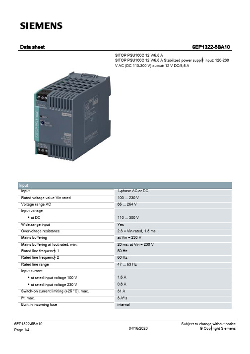
西门子SITOP PSU100C 12 V 6.5 A电源说明书
04/16/2020
Subject to change without notice © Copyright Siemens
Protection in the mains power input (IEC 898)
Output Output Rated voltage Vout DC Total tolerance, static ± Static mains compensation, approx. Static load balancing, approx. Residual ripple peak-peak, max. Residual ripple peak-peak, typ. Spikes peak-peak, max. (bandwidth: 20 MHz) Spikes peak-peak, typ. (bandwidth: 20 MHz) Adjustment range Product function Output voltage adjustable Output voltage setting Status display On/off behavior Startup delay, max. Voltage rise, typ. Rated current value Iout rated Current range ● Note Supplied active power typical Parallel switching for enhanced performance Numbers of parallel switchable units for enhanced performance
50 mm 50 mm 0 mm 0 mm 0.32 kg Yes
MMBQ11 Wi-Fi Module 规格说明书
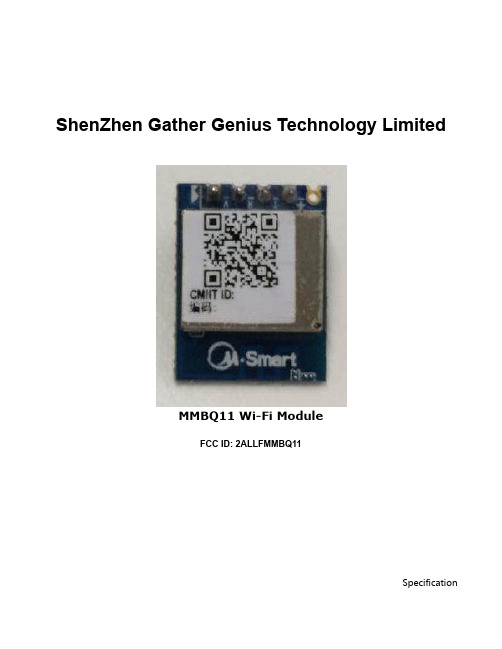
ShenZhen Gather Genius Technology LimitedMMBQ11 Wi-Fi ModuleFCC ID: 2ALLFMMBQ11SpecificationMMBQ11 WIFI Module DatasheetVersion 1.1 Disclaimer and noticeThe document is provided “AS IS,”without warranty of any kinds, including the implied warranties of merchantability and applies to any guarantee for a particular purpose, or non infringement, and any proposal, specification or sample of any guarantee mentioned anywhere else.This document does not bear any responsibility, including the use of the document information from infringement of any patent infringement liability.This document is not here by estoppel or otherwise, any intellectual property rights is granted the license, whether express or implied license.The information in this document might be modified for upgrade or other reasons.ShenZhen Gather Genius Technology Limite reserves the rights to make change withoutnotice. This document is used for design guide only, ShenZhen Gather Genius Technology Limitedtry the best to supply the correct information, but it does not assure there is not any error in this document. All the ostensive or implied states, information, suggestion are not guaranteed.INDEX1.GENERAL DESCRIPTION (2)1.1.Features (2)2.Pin assignment (4)3.Package and dimensions (5)4.Main function description (6)4.1.MCU (6)4.2.Memory (6)4.3.Interface (6)4.4.Absolute maximum ratings (6)4.5.Recommended operating range (7)5.RF specification (7)6.Power consumption (8)7.Recommended Reflow Profile (8)8.AT instruction (10)8.1.General AT instruction description (10)8.2.Operation instruction description (11)8.3.TCP/UDP port (14)8.4.GPIO/PWM instructions description (16)8.5.SMART LINK instruction description (17)8.6.SOFT AP instructions description (17)8.7.RF instructions description (18)8.8.Other description (23)1.GENERAL DESCRIPTIONThe MMBQ11module supports standard IEEE802.11 b/g/n protocol, TCP/IP stack and support STA, AP, STA+AP work mode. It can be used in the present device for additional Wi-Fi feature, or to design standalone network controller.MMBQ11 is a total solution for Wi-Fi network, which can be used separately.It can boot from external flash directly and designed to work with external MCU.In this case, MMBQ11can be added to any micro-controller system through UART interface.MMBQ11 is highly integrated with antenna switch, BALUN, PA, PMU. It just needs a few components for external circuit, which help to save the PCB room and cost furthest.1.1.Features•Support 802.11 b/g/n;•Embedded TCP/IP protocol stack;•Integrated TR switch/Balun/LNA/PA/antenna;•MCU clock frequency up to 160M, internal cache 8kB;•Integrated 16Mbitsflash;•Supply voltage range: 4.75V~5.25VDC, single 5V is recommended to use.•Support OTA firmware upgrade, which can be initiated with mobile phone APP and AT command;•Support STA, AP ,AP+STA mode;•Support Smart Link;•Support WEP/TKIP/WPA/WPA2 protocol;•Support802.11e and WMM/WMM PS;•Support UART;•Support HT20/40;Table 1 Major hardware and software features2.Pin assignmentThere are 4pins in MMBQ11 module, Figure1 is the pin assignment, Table 2 is the pin definition.Figure 1MMBQ11 pin assignmentTable 2 MMBQ11 pin definition3.Package and dimensionsThe dimensions of MMBQ11 module is 15mm*20mm*9.5mm(Figure 3), and it integrates 16Mb SPI Flash and 0 dBi PCB antenna.Figure 2MMBQ11module exteriorFigure 3MMBQ11 module dimensions4.Main function description4.1.MCUThe MCU of MMBQ11 is a low-power single chip, it supply integrated solution for embedded smart family system. It integrated 2.4 GHz WLAN CMOS PA and LNA. The RF front-end is single-ended double-direction. Also, it integrates LDO and DC-DC converter, which can separate digital circuit and analog circuit for lower noise.4.2.Memory4.2.1. Built- in SRAMMMBQ11 integrates 192KB SRAM。
SCALANCE X101-1 商品说明书
24 V
6GK5101-1BB00-2AA3 Page 1/4
06/28/2018
Subject to change without notice © Copyright Siemens
● at DC / maximum
Supply voltage, current consumption, power loss Supply voltage ● external ● external Type of voltage / of the supply voltage Product component / fusing at power supply input Fuse protection type / at input for supply voltage Consumed current ● maximum Power loss [W] ● at DC / at 24 V
Compact 40 mm 125 mm 124 mm 0.55 kg
Yes Yes Yes
No No
FM3611: Class 1, Divison 2, Group A, B, C, D / T.., Class 1, Zone 2, Group IIC, T.. EN 600079-15 II 3 G EEx nA II T.. KEMA 06 ATEX 0021 X
Yes
Yes Yes Yes Yes Yes No 134 y
/snst
/simatic-net https:// /industry/infocenter /bilddb /cax https://
Security information
UL 60950-1, CSA C22.2 No. 60950-1 UL 1604 and UL 2279-15 (Hazardous Location), Class 1 / Division 2 / Group A, B, C, D / T.., Class 1 / Zone 2 / Group IIC / T.. EN 61000-6-3 EN 61000-6-4:2001 EN 61000-6-2:2001, EN 61000-6-4:2001 Yes Yes Yes
PMS150C datasheet V001_CN-1

PMS150C系列8位IO类型单片机数据手册第0.01版2016年3月17日Copyright 2016 by PADAUK Technology Co., Ltd., all rights reserved重要声明应广科技保留权利在任何时候变更或终止产品,建议客户在使用或下单前与应广科技或代理商联系以取得最新、最正确的产品信息。
应广科技不担保本产品适用于保障生命安全或紧急安全的应用,应广科技不为此类应用产品承担任何责任。
关键应用产品包括,但不仅限于,可能涉及的潜在风险的死亡,人身伤害,火灾或严重财产损失。
应广科技不承担任何责任来自于因客户的产品设计所造成的任何损失。
在应广科技所保障的规格范围内,客户应设计和验证他们的产品。
为了尽量减少风险,客户设计产品时,应保留适当的产品工作范围安全保障。
PMS150C不适用于交流供电阻容降压或者电源纹波大,EFT要求高的应用,请注意不要将PMS150C用于这种特殊要求的产品中。
提供本文档的中文简体版是为了便于了解,请勿忽视文中英文的部份,因为其中提供有关产品性能以及产品使用的有用信息,应广科技暨代理商对于文中可能存在的差错不承担任何责任,建议参考本档英文版。
目录1. 单片机特点 (7)1.1. 系统功能 (7)1.2. CPU特点 (7)2. 系统概述和方框图 (8)3. 引脚功能说明 (9)4. 器件电气特性 (10)4.1 直流交流电气特性 (10)4.2 工作范围 (11)4.3 IHRC频率与VDD关系曲线图 (12)4.4 ILRC频率与VDD关系曲线图 (12)4.5 IHRC频率与温度关系曲线图(校准到16MHz) (13)4.6 ILRC频率与温度关系曲线图 (13)4.7 工作电流与VDD、系统时钟CLK=IHRC/n曲线图 (14)4.8 工作电流与VDD、系统时钟CLK=ILRC/n曲线图 (14)4.9 引脚上拉电阻曲线图 (15)4.10 引脚输出驱电流(Ioh)与灌电流(Iol) 曲线图 (15)4.11 引脚输出输入高电压与低电压(V IH / V IL) 曲线图 (16)5. 功能概述 (17)5.1程序内存——OTP (17)5.2 开机流程 (17)5.3 数据存储器 – SRAM (18)5.4 振荡器和时钟 (18)5.4.1内部高频振荡器和内部低频振荡 (18)5.4.2芯片校准 (18)5.4.3 IHRC频率校准与系统时钟 (19)5.4.4系统时钟和LVR基准位 (20)5.5 16位定时器 (Timer16) (21)5.6 看门狗定时器 (22)5.7 中断 (22)5.8 省电与掉电 (24)5.8.1省电模式(stopexe) (24)5.8.2掉电模式(stopsys) (25)5.8.3 唤醒 (26)5.9 IO引脚 (27)5.10 复位和LVR (28)5.10.1复位 (28)6. IO 寄存器 (29)6.1 标志寄存器(flag),IO 地址 =0x00 (29)6.2 堆栈指针寄存器(sp),IO地址 =0x02 (29)6.3 时钟控制寄存器(clkmd),IO地址 =0x03 (29)6.4 中断允许寄存器(inten),IO地址 =0x04 (30)6.6 Timer16控制寄存器(t16m),IO地址 =0x06 (30)6.7 外部晶体振荡器控制寄存器(eoscr,只写),IO地址 =0x0a (31)6.8 中断缘选择寄存器 (integs), IO地址 =0x0c (31)6.9 端口A数字输入启用寄存器(padier), IO 地址 =0x0d (31)6.10 端口A数据寄存器(pa),IO地址 =0x10 (31)6.11 端口A控制寄存器(pac),IO地址 =0x11 (31)6.12 端口A上拉控制寄存器(paph),IO地址 =0x12 (31)6.13 杂项寄存器(misc), IO 地址 =0x3b (32)7. 指令 (33)7.1 数据传输类指令 (34)7.2 算术运算类指令 (36)7.3 移位元元运算类指令 (38)7.4 逻辑运算类指令 (39)7.5 位运算类指令 (41)7.6 条件运算类指令 (41)7.7 系统控制类指令 (42)7.8 指令执行周期综述 (44)7.9 指令影响标志的综述 (45)8. 特别注意事项 (46)8.1. 使用IC时 (46)8.1.1. IO使用与设定 (46)8.1.2. 中断 (46)8.1.3. 切换系统时钟 (47)8.1.4. 掉电模式、唤醒以及看门狗 (47)8.1.5. TIMER16溢出时间 (47) (47)8.1.6. LVR8.1.7. 指令 (47)8.1.8. RAM定义限制 (47)8.1.9. 烧录方法 (48)8.2. 使用ICE时 (48)修订历史:修订日期描述初版0.01 2016/3/17PMS150B 和PMS150C 主要差异表PMS150B 与PMS150C 主要差异列举如下:项目 功能PMS150BPMS150C1 ILRC 频率 110KHz@5.0V ,25oC 62KHz@5.0V ,25o C (VDD 变化对ILRC 有影响) 2 LVR 2.8V,2.2V,2.0V 4.0V,3.5V,3.0V,2.75V 2.5V,2.2V,2.0V,1.8V 3 RAM 60 bytes64 bytes 4 PA5口输入模式上拉电阻 没有有5 工作温度0o C ~70o C -20o C ~70o C6省电模式功耗(stopexe ) 40uA@3.3V3 uA@3.3V7 IO 输出电流 17mA/-7mA@5.0V普通模式:14.5mA/-10.5mA@5.0V低驱动模式:5mA/-3.5mA@5.0V 8 看门狗定时器溢时 4096,16384,65536 ILRC 时钟周期8192,16384,65536,262144 ILRC 时钟周期9 唤醒时间 快速模式:1024 T IHRC 普通模式:1024 T ILRC 快速模式:32 T ILRC 普通模式:2048 T ILRC 10 开机时间快速模式:2048 T IHRC 普通模式:1024 T ILRC快速模式:32 T ILRC 普通模式:2048 T ILRC 11系统保留OTP 区 0x3F8~0x3FF(8 word) 0x3F0~0x3FF(16 word)12 ILRC 做系统时钟源 ILRC,ILRC/4 ILRC,ILRC/4,ILRC/16 13支持ICE 类型PDK3S-I-001/002/003, 5S-I-S015S-I-S011. 单片机特点1.1. 系统功能◆时钟模式:内部高频振荡器、内部低频振荡器◆硬件16位定时器◆快速唤醒功能◆ 6 个带输入上拉电阻IO引脚,且做输出时具有可选的电流驱动能力◆1个外部中断输入引脚◆每个引脚都可弹性设定唤醒功能◆8级LVR可选◆工作频率0 ~ 8MHz@VDD≧3V; 0 ~ 4MHz@VDD≧2.2V; 0 ~ 2MHz@VDD≧2.0V;◆工作电压:2.0V ~ 5.5V◆工作温度:-20 o C ~70 o C◆功耗特性:I operating ~ 0.3mA@1MIPS, VDD=3.3VI operating ~ 13uA@ILRC=62KHz, VDD=3.3VI powerdown ~ 0.5uA@VDD=3.3V1.2. CPU特点◆工作模式:单一处理单元的工作模式◆ 1KW OTP程序内存◆ 64字节数据存储器◆提供79条指令◆绝大部分指令都是单周期(1T)指令◆可程序设定的堆栈深度◆所有的数据存储器都可当数据指针(index pointer)◆独立的IO地址以及存储地址方便程序开发2. 系统概述和方框图PMS150C是一个IO类型、完全静态,以OTP为程序存储基础的单片机。
BradyPrinter i5100 使用者手冊说明书
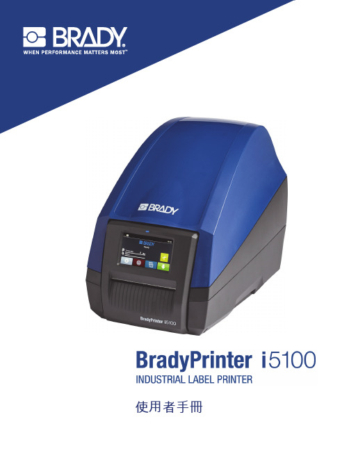
使用者手冊目錄1 • 簡介與安全警告 (1)一般資訊與免責聲明 (1)安全 (3)2 • 支援 (4)技術支援與維修 (4)應用工程服務 (5)3 • 設定與入門 (6)印表機組件概觀 (7)連接印表機 (8)4 • 觸控式螢幕 - 基本資訊 (10)首頁螢幕資訊 (10)首頁螢幕上的活動功能表圖示 (10)首頁螢幕頂部的資訊圖示 (11)首頁螢幕上的 IP-Enabled 耗材資訊 (11)基本功能表導覽 (12)5 • 列印模式 (14)智慧列印系統 (14)Brady 模式列印(IP-Enabled 列印) (14)標準模式列印 (14)部分 Brady 模式/部分標準模式 (14)有關 IP-Enabled 列印元件的其他資訊 (16)6 • 載入耗材 (17)載入順序 (17)取出已安裝的耗材 (17)載入標籤卷 (18)載入層迭標籤媒體 (20)載入色帶卷 (20)選擇和設定標籤感應器 (22)7 • 列印 (26)校準(列印媒體饋送的同步) (26)撕紙模式列印 (26)自動切割列印 (26)8 • 清潔與維護 (28)認可的清潔棉簽 (28)清潔列印輥 (28)清潔列印頭 (28)清潔標籤感應器 (28)清潔切刀(自動切刀型號) (29)9 • 故障排除 (30)錯誤螢幕導覽 (30)帶有補救方法的錯誤訊息清單 (30)10 • 媒體尺寸規格 (36)標籤/列印媒體尺寸 (36)印表機和感應器尺寸 (37)反射標記尺寸(「黑色標記」) (38)槽口/切口尺寸 (38)11 • 授權與機構許可 (40)1 • 簡介與安全警告一般資訊與免責聲明以下產品的使用者手冊:免責聲明本手冊是 Brady Worldwide, Inc.(後文稱為「Brady」)的專有財產,可能會不時進行修改,恕不另行通知。
Brady 不承擔為您提供此類 修改(如果有)的責任。
我們保留本手冊的所有著作權。
若無 Brady 的事先書面同意,不得使用任何方式複製或複製本手冊的任何部分。
YSI X100 Series 产品说明书
Transmitter x100e Seriesfor pH, Dissolved Oxygen and ConductivityAdvanced transmitters for reliable measurements and for harsh conditions Technical DataDrawings2Specifications transmitter pH 2100e 4Specifications transmitter O 24100e 6Specifications transmitter O 24100ppb 7Specifications transmitter Cond 7100e 8Specifications transmitter Cond Ind 7100e 10Terminal assignment «Advanced Line» transmitters 12General specifications «Advanced Line» transmitters 14Ordering information17Short descriptionThe cost-effective Transmitter X100 Series are suitable designed for highly reliable and accurate measure-ments in a wide range of industrial applications. The instruments are easy to operate and the large-size LCD provides substantial all essential information. The measurement values are displayed in largecharacters and additional pictographs explain the function operation and advise any signal or functional irregularities.Features–Two 0/4…20 mA current outputs –Two limit contacts –Alarm & wash contact–Continuous monitoring of sensor and transmitter performance –Sensor diagnostics–Easy operation with help of pictographs –PID controller–Communication with EasyClean, the METTLER TOLEDO cleaningContentsDrawings AssemblyMounting1Sealing plugs2Hexagon nuts3Pg cable glands4Rubber reducer5Pg plug6Enclosure screws7Hinge pin8Cable ties9Filler plugs10Gaskets11Washer12Jumper876541Cable gland (3 pieces)2Breakthroughs for cablegland or conduit 1/2 ",Ø 21.5 mm(2 breakthroughs).Conduits not included!3Holes for post mounting4Holes for wall mountingDrawingsPipe mounting with ZU 0274 bracket kitProtective hood ZU 0276 for wall and pipe mountingPanel-mount kit ZU 0275165 mm 132 mm173 m m1 Protected hood (if required)2 Hose clamps with worm gear drive to DIN 3017(2 pieces)3 Postmounting plate4 For vertical orhorizontal post/pipe mounting5 Self-tapping screws1 Screws2 Seal3 Control panel4 Span pieces5 Threaded sleevesSpecifications Transmitter pH 2100e pH/mV input Input for pH, ORP electrodes or ISFETMeasurement range –1500…+1500 mVDisplay range pH value –2.00…16.00ORP –1999…+1999 mVGlass electrode input1)Input resistance > 0.5 x 10 12ΩInput current < 2 x 10 –12AReference electrode input1)Input resistance > 1 x 10¹⁰ΩInput current < 1 x 10 –10AMeas. error 1,2,3)pH value< 0.02mV value< 1 mVElectrodestandardization pH *Operating modes-BUF Calibration with automatic buffer recognition Calimatic:Buffer sets-01-Mettler-Toledo 2.00/4.01/7.00/9.21-02-Merck/Riedel de Haen 2.00/4.00/7.00/9.00/12.00-03-Ciba (94) 2.06/4.00/7.00/10.00-04-NIST technical 1.68/4.00/7.00/10.01/12.46-05-NIST standard 1.679/4.006/6.865/9.180-06-HACH 4.00/7.00/10.18-07-WTW technical buffers 2.00/4.01/7.00/10.00-PRD Product Calibration-MAN Calibration with manual entry of individual buffer values-DAT Data entry of premeasured electrodesZero point adjustment ±200 mVMax. calibration range Asymmetry potential: ±60 mVSlope: 80…103 % (47.5…61 mV/pH)Sensor standardizationORP*ORP calibrationMax. calibration range –700…+700D mVCal timer 0000…9999 hSensocheck automatic monitoring of glass andreference electrode (can be disabled)Sensoface provides information on the electrode condition.Evaluation of zero/slope, response,calibration interval, SensocheckSpecifications Transmitter pH 2100e Temperature input *Pt100/Pt1000/NTC 30 kΩ / NTC 8,55 kΩ2-wire connection, adjustableMeasurement range Pt100/Pt1000: –20.0…+ 200.0 °C/–4…+ 392 °FNTC 30 kΩ – 20.0…+ 150.0 °C/–4…+ 302 °FNTC 8.55 kΩ –10.0…+ 130.0 °C/+14…+ 266 °FAdjustment range 10 KResolution0.1 °C/1 °FMeas. error 1,2,3)< 0.5 K (< 1 K for Pt100; <1K for NTC >100 °C)Temp. compensation Linear –19.99…+19.99 %/Kof process medium (reference temp. 25 °C)Power output for operating an ISFET adapter+ 3 V/0.5 mA– 3 V/0.5 mA*User-defined1)To IEC 746 Part 1, at nominal operating conditions2)± 1 count3)Plus sensor errorSpecifications Transmitter O24100e Dissolved oxygen inputSensor type A:InPro6000 (6800)Sensor type B:InPro6900Measuring current-2…1800 nAResolution0.05 nA (with Vpol ≤ 800 mV and Vref ≤ 200 mV)Saturation (–10…80 °C)0…500 %Meas. error1,2,3)0.5 % of meas. val. +0.5 %Concentration (–10…80 °C)0.00…50.00 mg/l0.00…50.00 ppmMeas. error 1,2,3)0.5 % of meas. val. + 0.05 mg/lor 0.05 ppmAdm. guard current20 µAPolarization voltage * 0…1000 mVProcess pressure* 0.000…9.999 bar(…999.9 kPa/…145.0 psi)Salt correction * 00.00…45.00 g/kgSensor standardizationOperating modes * DO saturation (automatic)DO concentration (automatic)Product calibrationZero point calibrationCalibration range Zero point ± 2 nASensor type A Slope 25…130 nA(at 25 °C, 1013 mbars)Calibration range Zero point ± 2 nASensor type B Slope200…550 nA(at 25 °C, 1013 mbars)Calibration timer * 0000…9999 hPressure correction * 0.000…9.999 bars/999.9 kPa/145.0 psiSensocheck Monitoring for short circuits/open circuits (can be disabled)Sensoface Provides information on the sensor conditionEvaluation of zero/slope, response, calibration interval, SensocheckTemperature input *NTC 22 kΩ / NTC 30 kΩ*2-wire connection, adjustableMeasurement range– 20.0…+150.0 °C/– 4…+ 302 °FAdjustment range10 KResolution0.1 °C/1 °FMeas. error 1,2,3)< 0.5 K (< 1 K at >100 °C)*User-defined1)To IEC 746 Part 1, at nominal operating conditions2)± 1 count3)Plus sensor errorSpecifications Transmitter O24100ppb Dissolved oxygen inputSensor type A:InPro6000 (6800)Sensor type B:InPro6900Measuring current-2…600 nAResolution0.01 nA (with Vpol ≤ 500 mV and Vref ≤ 200 mV)Saturation (–10…80 °C)0.0.…120.0 %Meas. error1,2,3)0.5 % of meas. val. +0.1 %Concentration (–10…80 °C)0000…9999 µg/l0000…9999 ppb0.0000…9.999 mg/l0.0000…9.999 ppmMeas. error 1,2,3)0.5 % of meas. val. +0.005 mg/lor 0.005 ppmAdm. guard current20 µAPolarization voltage* 0…1000 mVProcess pressure* 0.000…9.999 bars(to 999.9 kPa/…145.0 psi)Salt correction* 00.00…45.00 g/kgSensor standardizationOperating modes * DO saturation (automatic)DO concentration (automatic)Product calibrationZero point calibrationCalibration range Zero point ± 2 nASensor type A Slope25…130 nA(at 25 °C, 1013 mbars)Calibration range Zero point ± 2 nASensor type B Slope 200…550 nA(at 25 °C, 1013 mbars)Calibration timer * 0000…9999 hPressure correction * 0.000…9.999 bars/999.9 kPa/145.0 psiSensocheck Monitoring for short circuits/open circuits (can be disabled)Sensoface Provides information on the sensor conditionEvaluation of zero/slope, response, calibration interval, SensocheckTemperature input *NTC 22 kΩ/ NTC 30 kΩ*2-wire connection, adjustableMeasurement range–20.0…+150.0 °C/–4…+302 °FAdjustment range10 KResolution0.1 °C/1 °FMeas. error 1,2,3)< 0.5 K (< 1 K at >100 °C)*User-defined1)To IEC 746 Part 1, at nominal operating conditions2)± 1 count3)Plus sensor errorSpecifications Transmitter Cond 7100e Conductivity input Input for 2-e or 4-e conductivity sensorsWorking range4-electrode sensor:0.2 µS *c …1000 mS * c (c = cell constant)2-electrode sensor:0.2 µS *c …200 mS * c(the actual range is very much depending on the sensor used,display limited to 3500 mS)Effective ranges Conductivity0.000…9.999 µS/cm00.00…99.99 µS/cm000.0…999.9 µS/cm0000…9999 µS/cm0.000…9.999 mS/cm00.00…99.99 mS/cm000.0…999.9 mS/cm0.000…9.999 S/m00.00…99.99 S/mResistivity00.00…99.99 MΩcmConcentration0.00…9.99 % by wt.Salinity0.0…45.0 ‰ (0…35 °C)Measurement error1,2,3)< 1% of measured value +0.4 µS * cConc. measurements-01- NaCl0.00…9.99 % by wt.(0 …60°C)-02- HCl0.00…9.99 % by wt.(–20…50 °C)-03- NaOH0.00…9.99 % by wt.(0…100 °C)-04- H2SO40.00…9.99 % by wt.(–17…110 °C)-05- HNO30.00…9.99 % by wt.(–17…50 °C)Sensor standardization Input of cell constant with simultaneous displayof conductivity value and temperatureInput of conductivity value with simultaneous displayof cell constant and temperatureProduct calibrationTemperature probe adjustmentPermissible cell constant00.0050…19.9999 cm–1Sensocheck Monitoring of sensor polarization and cable capacitance (can be disabled)Sensoface Provides information on the sensor condition (Sensocheck)Sensor monitor Display of direct measurement values for validationpurpose (resistance/temperature)USP-Function Monitoring of conductivity of water for pharmaceuticalapplications to USP (USP <645>) with adjustable limitvalues (10…100 % of USP value)Specifications Transmitter Cond 7100e Temperature input*)Pt100/Pt1000/NTC 30 kΩ / NTC 8.55 kΩ2-wire connection, adjustableMeasuring range Pt100/Pt1000–20…+200 °C / –4…+392 °FNTC 30 kΩ–20…+150 °C / -4…+302 °FNTC 8.55 kΩ–10…+130 °C / +14…+266 °FResolution0.1 °C / 1 °FError1,2,3)0.5 K (< 1 K with Pt100; < 1 K with NTC > 100 °C)Temperature compensation(OFF)not compensated(ref. temp. 25 °C)(Lin)linear, 0.00…19.99 %/K, –20…130 °C(NLF)natural waters to EN 27888, 0…36 °C(nACL)ultrapure water with NaCl traces, 0…120 °C(HCL)ultrapure water with HCl traces, 0…120 °C(nH3)ultrapure water with NH3traces, 0…120 °C*User-defined1)To IEC 746 Part 1, at nominal operating conditions2)± 1 count3)Plus sensor errorSpecifications Transmitter Cond Ind 7100e Conductivity input Input for inductive sensorsWorking range Conductivity0.000…1999 mS/cmConcentration0.00…100 % by wt.Salinity0.0…45.0 ‰ (0…35 °C)Effective ranges Conductivity0.000…9.999 mS/cm00.00…99.99 mS/cm000.0…999.9 mS/cm0000…1999 mS/cm0.000…9.999 S/m00.00…99.99 S/mConcentration0.00…99.99 %Salinity0.0…45.0 ‰ (0…35 °C)Measurement error1,2,3)< 1% of measured value +0.005 mSConc. measurements-01- NaCl0…26 %(0…60 °C)-02- HCl0…18 % (–20…50 °C)-03- NaOH0…14 % (0…100 °C)-04- H2SO40…30 % (–17…110 °C)-05- HNO30…30 % (–20…50 °C)-06- H2SO492…99 % (–17…115 °C)-07- HCl22…39 % (–20…50 °C)-08- HNO335…96 % (–20…50 °C)-09- H2SO432…84 % (–17…115 °C)-10- NaOH18…50 % (0…100 °C)Sensor standardization Input of cell factor with simultaneous displayof conductivity value and temperatureInput of conductivity value with simultaneous displayof cell factor and temperatureProduct calibrationZero point calibrationTemperature probe adjustmentPermissible cell factor00.100…19.999Permissible transfer ratio01.00…199.99Permissible zero pointdeviation± 0.5 mS/cmSensocheck Monitoring of sender coil and leads for short circuiting,and of the receiver coil for disruption (can be disabled)Sensoface Indicates sensor status (zero point, sensocheck)Sensor monitor Display of direct measurement values for validationpurpose (resistance /temperature)Specifications Transmitter Cond Ind 7100e Temperature input*Pt100/Pt1000/NTC 100 kΩ2-wire connection, adjustableMeasuring range Pt100/Pt1000–20…+200 °C / –4… +392 °FNTC–20…+130 °C / –4… +266 °FResolution0.1 °C / 1 °FError1,2,3)0.5 K (< 1 K with Pt100; < 1 K with NTC > 100 °C)Temperature compensation(OFF)not compensated(ref. temp. 25 °C)(LIN)linear, 0.00…19.99 %/K(NLF)natural waters to EN 27888 (0…35 °C)* User-defined1) To IEC 746 Part 1, at nominal operating conditions2) ± 1 count3) Plus sensor errorTerminal assignment «Advanced Line» transmittersTransmitter O 24100 ppbTransmitter O 24100 eTransmitter pH 2100 eTerminal assignment«Advanced Line» transmitters Transmitter Cond 7100eTransmitter Cond Ind 7100eGeneral specifications «Advanced Line» transmitters HOLD input Galv. separated (OPTO coupler)Function Switches device to HOLD stateSwitching voltage 0…2 V (AC/DC) hold inactive10…30 V (AC/DC) hold activeCONTROL input pH/O2)Galv. separated (OPTO coupler)Function Control input for automatic cleaning/calibration systemSwitching voltage0…2 V (AC/DC) inactive10…30 V (AC/DC) activeCONTROL input (Cond)Galv. separated (OPTO coupler)Function Switches between two parameter setsSwitching voltage0…2 V (AC/DC) set #1 active10…30 V (AC/DC) set #2 activeOutput 10/4…20 mA, max. 10 V, floating(galv. connected to output 2)Process variable *pH 2100 e pH/mVO24100e%, mg/lO24100 ppb%, mg/lCond 7100e conductivity, resistivity, concentration, salinityCond Ind 7100e conductivity, concentration, salinityCurrent characteristics*linear or logarithmic (depends on transmitter)Overrange *22 mA in the case of error messageOutput filter *Low-pass, filter time constant 0…120 sMeas. error1)< 0.3 % of current value +0.05 mAStart/end of scale As desired within measuring rangeAdm. span pH 2100e 2.00…18.00/200…3000 mV024100e 5…500 %, 0.5…50 mg/l024100 ppb 2…200 %, 0.2…10 mg/lCond 7100e LIN 5 % of selected measuring rangeLOG 1 decadeCond Ind 7100e LIN 5 % of selected measuring rangeLOG 1 decadeOutput 20/4…20 mA, max. 10 V, floating(galv. connected to output 1)Process variable TemperatureOverrange *22 mA in the case of temp error messagesOutput filter *Low-pass, filter time constant 0…120 sMeas. error 1)< 0.3 % of current value + 0.05 mAStart/end of scale *pH, Cond: –20…+200 °C/–4…+392 °F, 02:–20…+150 °C/–4...+302 °FAdm. span pH, Cond: 20…320 K, 02:20…170 KAlarm contact Relay contact, floatingContact ratings AC < 250 V/< 3 A/< 750 VADC < 30 V/< 3 A/< 90 WContact response N/C (fail-safe type)Alarm delay 0000…0600 sGeneral specifications «Advanced Line» transmitters Limit values Output via relay contacts R1, R2Contacts R1, R2 floating, but inter-connectedContact ratings AC < 250 V/< 3 A/< 750 VADC < 30 V/< 3 A/< 90 WContact response *N/C or N/ODelay *0000…9999 sSwitching points *As desired within measuring rangeHysteresis *pH 2100e0…5.00 pH/0…500 mV024100e 0…50 %/0…5.00 mg/l (ppm)024100ppb 0…50 %/0…5.00 mg/l (ppm)Cond 7100e0…50 % of measuring rangeCond Ind 7100e0…50 % of measuring rangePID process controller Output via relay contacts R1, R2 (see limit values)Setpoint specification *pH 2100e–02.00…16.00/– 1500…+1500 mV024100e 0…500 % / 0…50 mg/l024100ppb 0…120% / 0…9.999 mg/lCond 7100e within selected measuring rangeCond Ind 7100e within selected measuring rangeNeutral zone *pH 2100e0…5.00 pH / 0…+500 mV024100e 0…50 % / 0…5 mg/l024100ppb 0…50 % / 0…5 mg/l (ppm)Cond 7100e within selected measuring rangeCond Ind 7100e max. 50 % of selected measuring rangeP-action *Controller gain K R:0010…9999 %I-action component *Reset time Tr: 0000…9999 s(0000 s = no integral action)D-action component *Derivative-actiontime Td: 0000…9999 s(0000 s = no derivative action)Controller type*Pulse length controller or pulse frequency controllerPulse period *0001…0600 s, min. ON time 0.5 s (pulse length controller)Max. pulse frequency *0001…0180 min–1(pulse frequency controller)Cleaning function/Relay contact, floating2nd parameter set for controlling a simple rinsing system or an automatic cleaning systemor to show that 2nd parameter set is activeContact ratings AC < 250 V/< 3 A/< 750 VADC < 30 V/< 3 A/< 90 WContact response *N/C or N/O (cleaning function)N/O (2nd parameter set)Rinsing interval *000.0…999.9 h(000.0 h = cleaning function switched off)Cleaning time *0000…1999 sCalibration interval *000.0…999.9 hCleaning interval*000.0…999.9 h*User-defined1)To IEC 746 Part 1, at nominal operating conditions2)± 1 count3)Plus sensor errorGeneral specifications«Advanced Line» transmitters Display LC display, 7-segment with iconsMain display Character height 17 mm, unit symbols 10 mmSecondary display Character height 10 mm, unit symbols 7 mmSensoface 3 status indicators (friendly, neutral, sad smiley)Mode indicators 5 status bars: «meas», «cal», «alarm», «cleaning», «config»18 further icons for configuration and messagesAlarm indication Red LED in case of alarm or HOLD, user definedKeypad 5 keys: [cal] [conf] [] [] [enter]Service functionsCurrent source Current specifiable for output 1 and 2 (00.00…22.00mA)Manual controller Controller output entered directly (start of control process)Device self-test Automatic memory test (RAM, FLASH, EEPROM)Display test Display of all segmentsLast Error Display of last error occurredSensor monitor Display of direct, uncorrected sensor signal (electrode/sensor)Relay test Manual control of the four switching contactsParameter sets*Two selectable parameter sets for different applicationsData retention Parameters and calibration data > 10 years (EEPROM)EMC EN 61326EN 61326/A1Lightning protection EN 61000-4-5, Installation Class 2Protection against Protective separation of all extra-low-voltageelectrical shock circuits against mains as per EN 61010FM/CSA NI, Class 1, Div 2, Group A, B, C, D, T4Power supply24 (–15%)…230 (+10%) V AC/DC; approx. 5 VA, 2.5 WAC: 45…65 HzOvervoltage category II, Class IINominal operating conditionsAmbient temperature– 20…+55 °C / –4...+131 °FTransport/Storage temp – 20…+70 °C / -4...+158 °FRelative humidity 10…95 % non condensingPower supply24 (–15%)…230 (+ 10 %) V AC/DCFrequency for AC 45…65 HzGeneral specifications and ordering information«Advanced Line» transmittersEnclosure molded enclosure made of PBT (polybutylene terephtalate)Color Bluish gray RAL 7031Assembly• Wall mounting• Pipe mounting: Ø 40…60 mm,Ø 30…45 mm• Panel mounting, cutout to DIN 43 700, sealed against panelDimensions H x W x L: 144 x 144 x 105 mm (5.67 x 5.67 x 4.13")Ingress protection IP 65/NEMA 4XCable glands 3 breakthroughs for cable glands M20 x 1.52 breakthroughs for NPT 1/2 " or Rigid Metallic ConduitWeight approx. 1 kg*User-defined1)To IEC 746 Part 1, at nominal operating conditions2)± 1 count3)Plus sensor errorOrdering information Array Transmitter pH 2100e pH 2100e52 121 102Transmitter O24100e O24100e52 121 103Transmitter O2 4100ppb O24100ppb52 121 104Transmitter Cond 7100e Cond 7100e52 121 126Transmitter Cond Ind 7100e Cond Ind 7100e52 121 127Installation accessoriesBracket kit ZU 027452 120 741Panel-mount kit ZU 027552 120 740Protective hood ZU 027652 120 739NotesNotesMETTLER TOLEDO Market Organizations Subject to technical changes.© Mettler-Toledo AG, Process Analytics 08/13 Printed in Switzerland. 52 121 132Mettler-Toledo AG, Process Analytics Im Hackacker 15, CH–8902 Urdorf Tel. + 41 44 729 62 11, Fax +41 44 729 66 Sales and Service:Australia Mettler-Toledo Ltd.220 Turner Street Port Melbourne AUS-3207 Melbourne/VIC Phone +61 1300 659 761Fax +61 3 9645 3935e-mail *****************Austria Mettler-Toledo Ges.m.b.H.Südrandstraße 17A-1230 Wien Phone +43 1 604 19 80Fax +43 1 604 28 80e-mail ***********************Brazil Mettler-Toledo Ind. e Com. Ltda.Avenida Tamboré, 418TamboréBR-06460-000 Barueri/SP Tel.+55 11 4166 7400Fax +55 11 4166 7401e-mail *******************.br *******************.br China Mettler-Toledo Instruments (Shanghai) Co. Ltd.589 Gui Ping Road Cao He Jing CN-200233 Shanghai Phone +86 21 64 85 04 35Fax +86 21 64 85 33 51e-mail *************** Croatia Mettler-Toledo d.o.o.Mandlova 3HR-10000 Zagreb Phone +385 1 292 06 33Fax +385 1 295 81 40e-mail ****************Czech Republic Mettler-Toledo s.r.o.Trebohosticka 2283/2CZ-100 00 Praha 10 Phone +420 2 72 123 150Fax +420 2 72 123 170e-mail *****************Denmark Mettler-Toledo A/S Naverland 8DK-2600 Glostrup Phone +45 43 27 08 00Fax +45 43 27 08 28e-mail ****************France Mettler-Toledo Analyse Industrielle S.A.S.30, Boulevard de Douaumont F-75017 Paris Phone +33 1 47 37 06 00Fax +33 1 47 37 46 26e-mail **************Germany Mettler-Toledo GmbH Prozeßanalytik Ockerweg 3D-35396 Gießen Phone +49 641 507 333Fax +49 641 507 397e-mail **************Great Britain Mettler-Toledo LTD 64 Boston Road, Beaumont Leys GB-Leicester LE4 1AW Phone +44 116 235 7070Fax +44 116 236 5500e-mail *******************Hungary Mettler-Toledo Kereskedelmi KFT Teve u. 41HU-1139 Budapest Phone +36 1 288 40 40Fax +36 1 288 40 50e-mail ***************India Mettler-Toledo India Private Limited Amar Hill, Saki Vihar Road Powai IN-400 072 Mumbai Phone +91 22 2857 0808Fax +91 22 2857 5071e-mail *****************Italy Mettler-Toledo S.p.A.Via Vialba 42I-20026 Novate Milanese Phone +39 02 333 321Fax +39 02 356 2973e-mail **************************Japan Mettler-Toledo K.K.Process Division 6F Ikenohata Nisshoku Bldg.2-9-7, Ikenohata Taito-ku JP-110-0008 Tokyo Phone +81 3 5815 5606Fax +81 3 5815 5626e-mail **********************Malaysia Mettler-Toledo (M) Sdn Bhd Bangunan Electroscon Holding, U 1-01Lot 8 Jalan Astaka U8/84Seksyen U8, Bukit Jelutong MY-40150 Shah Alam Selangor Phone +60 3 78 44 58 88 Fax +60 3 78 45 87 73e-mail ****************************Mexico Mettler-Toledo S.A. de C.V.Ejercito Nacional #340Col. Chapultepec Morales Del. Miguel Hidalgo MX-11570 México D.F.Phone +52 55 1946 0900e-mail *****************Poland Mettler-Toledo (Poland) Sp.z.o.o.ul. Poleczki 21PL-02-822 Warszawa Phone +48 22 545 06 80Fax +48 22 545 06 88e-mail *************Russia Mettler-Toledo Vostok ZAO Sretenskij Bulvar 6/1Office 6RU-101000 Moscow Phone +7 495 621 56 66Fax +7 495 621 63 53e-mail **************Singapore Mettler-Toledo (S) Pte. Ltd.Block 28Ayer Rajah Crescent #05-01SG-139959 Singapore Phone +65 6890 00 11Fax +65 6890 00 12+65 6890 00 13e-mail ****************Slovakia Mettler-Toledo s.r.o.Hattalova 12/A SK-83103 Bratislava Phone +421 2 4444 12 20-2Fax +421 2 4444 12 23e-mail *************Slovenia Mettler-Toledo d.o.o.Pot heroja Trtnika 26SI-1261 Ljubljana-Dobrunje Phone +386 1 530 80 50Fax +386 1 562 17 89e-mail *******************South Korea Mettler-Toledo (Korea) Ltd.Yeil Building 1 & 2 F 124-5, YangJe-Dong SeCho-Ku KR-137-130 Seoul Phone +82 2 3498 3500Fax +82 2 3498 3555e-mail *****************Spain Mettler-Toledo S.A.E.C/Miguel Hernández, 69-71ES-08908 L’Hospitalet de Llobregat (Barcelona)Phone +34 902 32 00 23Fax +34 902 32 00 24e-mail *************Sweden Mettler-Toledo AB Virkesvägen 10Box 92161SE-12008 Stockholm Phone +46 8 702 50 00Fax +46 8 642 45 62e-mail ****************Switzerland Mettler-Toledo (Schweiz) GmbH Im Langacher Postfach CH-8606 Greifensee Phone +41 44 944 45 45Fax +41 44 944 45 10e-mail ******************Thailand Mettler-Toledo (Thailand) Ltd.272 Soi Soonvijai 4Rama 9 Rd., Bangkapi Huay Kwang TH-10320 Bangkok Phone +66 2 723 03 00Fax +66 2 719 64 79e-mail ****************************USA/Canada Mettler-Toledo Ingold, Inc.36 Middlesex Turnpike Bedford, MA 01730, USA Phone +1 781 301 8800Freephone +1 800 352 8763Fax +1 781 271 0681e-mail**************。
LCB710;中文规格书,Datasheet资料
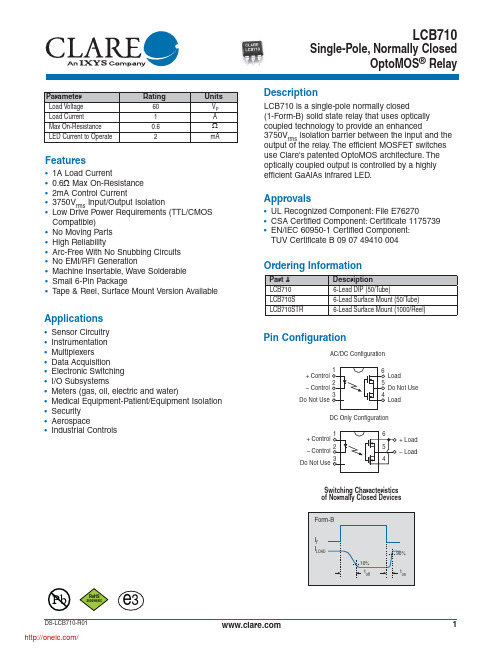
Applications
• Sensor Circuitry • Instrumentation • Multiplexers • Data Acquisition • Electronic Switching • I/O Subsystems • Meters (gas, oil, electric and water) • Medical Equipment-Patient/Equipment Isolation • Security • Aerospace • Industrial Controls
RoHS
2002/95/EC
DS-LCB710-R01
/
e3
Switching Characteristics of Normally Closed Devices
Form-B
IF ILOAD
10% toff
90% ton
1
Absolute Maximum Ratings @ 25ºC
Typical LED Forward Voltage Drop (N=50, TA=25ºC)
30
25
20
15
10
5
0 1.220 1.225 1.230 1.235 1.240 1.245 1.250 LED Forward Voltage (V)
Device Count (N)
PERFORMANCE DATA*
Ordering Information
Part # LCB710 LCB710S LCB710STR
Description 6-Lead DIP (50/Tube) 6-Lead Surface Mount (50/Tube) 6-Lead Surface Mount (1000/Reel)
NSi812x高可靠双通道数字隔离器数据手册说明书
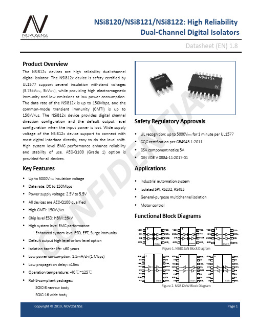
C O NF ID EN T IA LNSi8120/NSi8121/NSi8122: High ReliabilityDual-Channel Digital IsolatorsDatasheet (EN) 1.8Product OverviewThe NSi812x devices are high reliability dual-channel digital isolator. The NSi812x device is safety certified by UL1577 support several insulation withstand voltages (3.75kV rms , 5kV rms ), while providing high electromagnetic immunity and low emissions at low power consumption. The data rate of the NSi812x is up to 150Mbps, and the common-mode transient immunity (CMTI) is up to 150kV/us. The NSi812x device provides digital channel direction configuration and the default output level configuration when the input power is lost. Wide supply voltage of the NSi812x device support to connect with most digital interface directly, easy to do the level shift. High system level EMC performance enhance reliability and stability of use. AEC-Q100 (Grade 1) option is provided for all devices.Key Features• Up to 5000V rms Insulation voltage• Date rate: DC to 150Mbps• Power supply voltage: 2.5V to 5.5V • All devices are AEC-Q100 qualified • High CMTI: 150kV/us • Chip level ESD: HBM: ±6kV• High system level EMC performance:Enhanced system level ESD, EFT, Surge immunity• Default output high level or low level option • Isolation barrier life: >60 years• Low power consumption: 1.5mA/ch (1 Mbps) • Low propagation delay: <15ns • Operation temperature: -40℃~125℃ • RoHS-compliant packages:SOIC-8 narrow body SOIC-16 wide bodySafety Regulatory Approvals• UL recognition: up to 5000V rms for 1 minute per UL1577• CQC certification per GB4943.1-2011• CSA component notice 5A • DIN VDE V 0884-11:2017-01Applications• Industrial automation system • Isolated SPI, RS232, RS485• General-purpose multichannel isolation • Motor controlFunctional Block DiagramsC O NF ID EN T IA LIndex1.0 ABSOLUTE MAXIMUM RATINGS .............................................................................................................................. 3 2.0 SPECIFICATIONS ........................................................................................................................................................... 3 2.1. E LECTRICAL CHARACTERISTICS .................................................................................................................................................. 3 2.2. TYPICAL PERFORMANCE CHARACTERISTICS ........................................................................................................................... 7 2.3. P ARAMETER M EASUREMENT I NFORMATION . (8)3.0 HIGH VOLTAGE FEATURE DESCRIPTION (9)3.1. INSULATION AND SAFETY RELATED SPECIFICATIONS (9)3.2. DIN VDE V 0884-11(VDE V 0884-11):2017-01 INSULATION CHARATERISTICS ....................................................................... 9 3.3. R EGULATORY INFORMATION ................................................................................................................................................... 11 4.0 FUNCTION DESCRIPTION ..........................................................................................................................................11 5.0 APPLICATION NOTE ................................................................................................................................................... 12 5.1. PCB L AYOUT ...................................................................................................................................................................... 12 5.2. H IGH SPEED PERFORMANCE ................................................................................................................................................... 12 5.3. T YPICAL S UPPLY C URRENT E QUATIONS ..................................................................................................................................... 13 6.0 PACKAGE INFORMATION ......................................................................................................................................... 13 7.0 TAPE AND REEL INFORMATION ............................................................................................................................. 17 8.0 ORDER INFORMATION .............................................................................................................................................. 20 9.0 REVISION HISTORY . (21)C O NF ID EN T IA L1.0 ABSOLUTE MAXIMUM RATINGSPower Supply Voltage VDD1, VDD2 -0.5 6.5 V Maximum Input Voltage VINA, VINB -0.4 VDD+0.41 V Maximum Output Voltage V OUTA , V OUTB -0.4 VDD+0.41 VMaximum Input/Output Pulse VoltageVINA, VINB, V OUTA , V OUTB-0.8VDD+0.8VPulse width should be less than 100ns, and the duty cycle should be less than 10%Common-Mode Transients CMTI ±150 kV/us Output currentIo -15 15mAMaximum Surge Isolation VoltageV IOSM5.3kVOperating Temperature Topr -40125 ℃Storage Temperature Tstg -40150℃Electrostatic dischargeHBM±6000VCDM±2000V1 The maximum voltage must not exceed 6.5V.2.0 SPECIFICATIONS2.1. ELECTRICAL CHARACTERISTICS(VDD1=2.5V~5.5V, VDD2=2.5V~5.5V, Ta=-40℃ to 125℃. Unless otherwise noted, Typical values are at VDD1 = 5V, VDD2 = 5V, Ta =25℃)Power on ResetVDD POR2.2 V POR threshold as during power-upVDD HYS 0.1 V POR threshold Hysteresis Input ThresholdV IT1.6 V Input Threshold at rising edge V IT_HYS 0.4 V Input Threshold Hysteresis High Level Input Voltage V IH 2 V Low Level Input Voltage V IL 0.8 V High Level Output Voltage V OH VDD-0.3 V I OH ≤ 4mA Low Level Output VoltageV OL0.3VI OL ≤ 4mAC O NF ID EN T IA LOutput Impedance R out 50 ohm Input Pull high or low CurrentI pull 8 15 uA Start Up Time after POR trbs 40 usec Common Mode Transient ImmunityCMTI±100±150kV/us(VDD1=5V± 10%, VDD2=5V± 10%, Ta=-40℃ to 125℃. Unless otherwise noted, Typical values are at VDD1 = 5V, VDD2 = 5V, Ta = 25℃)Supply currentNSi8120 I DD1(Q0) 0.58 0.87 mAAll Input 0V for NSi8120x0 Or All Input at supply for NSi8120x1 I DD2(Q0) 1.18 1.77 mA I DD1(Q1) 2.92 4.38 mA All Input at supply for NSi8120x0 Or All Input 0V for NSi8120x1I DD2(Q1) 1.241.86mAI DD1(1M) 1.71 2.56 mA All Input with 1Mbps, C L =15pFI DD2(1M)1.382.07mAI DD1(10M) 1.78 2.67 mA All Input with 10Mbps, C L =15pF I DD2(10M)3.24.8mA I DD1(100M)2.103.15 mA All Input with 100Mbps, C L =15pFI DD2(100M)21.031.5mANSi8121/ NSi8122 I DD1(Q0) 1.031.55 mA All Input 0V for NSi812xx0 Or All Input at supply for NSi812xx1 I DD2(Q0) 1.00 1.5 mA I DD1(Q1)2.203.3 mA All Input at supply for NSi812xx0Or All Input 0V for NSi812xx1 I DD2(Q1)2.133.2 mA I DD1(1M) 1.72 2.58 mA All Input with 1Mbps, C L =15pFI DD2(1M) 1.68 2.52 mA I DD1(10M) 2.62 3.93 mA All Input with 10Mbps, C L =15pFI DD2(10M) 2.71 4.06 mA I DD1(100M) 11.01 16.5 mA All Input with 100Mbps, C L = 15pF I DD2(100M)12.8 19.2 mA Data RateDR 0 150 MbpsC O NF ID EN T IA LPropagation Delayt PLH 5 8.20 15 ns See Figure 2.7 , C L = 15pF t PHL 5 10.56 15 ns See Figure 2.7, C L = 15pF Pulse Width Distortion |t PHL – t PLH | PWD5.0nsSee Figure 2.7 , C L = 15pFRising Time t r 5.0 ns See Figure 2.7 , C L = 15pF Falling Timet f 5.0 ns See Figure 2.7 , C L = 15pFPeak Eye Diagram Jitter t JIT (PK) 350 ps Channel-to-Channel Delay Skewt SK (c2c) 2.5 nsPart-to-Part Delay Skewt SK (p2p)5.0ns(VDD1=3.3V± 10%, VDD2=3.3V± 10%, Ta=-40℃ to 125℃. Unless otherwise noted, Typical values are at VDD1 = 3.3V, VDD2 = 3.3V, Ta =25℃)Supply currentNSi8120 I DD1(Q0) 0.550.83mA All Input 0V for NSi8120x0 Or All Input at supply for NSi8120x1 I DD2(Q0) 1.12 1.68 mA I DD1(Q1) 2.87 4.3 mA All Input at supply for NSi8120x0 Or All Input 0V for NSi8120x1 I DD2(Q1)1.18 1.77mA I DD1(1M)1.72.55mA All Input with 1Mbps, C L = 15pFI DD2(1M)1.271.91 mA I DD1(10M) 1.732.6 mA All Input with 10Mbps, C L = 15pF I DD2(10M)2.413.6 mA I DD1(100M) 2.05 3.08 mA All Input with 100Mbps, C L = 15pF I DD2(100M)14.0521.08mANSi8121/ NSi8122 I DD1(Q0) 0.98 1.47 mA All Input 0V for NSi812xx0 Or All Input at supply for NSi812xx1 I DD2(Q0) 0.95 1.43 mA I DD1(Q1) 2.14 3.21 mA All Input at supply for NSi812xx0 Or All Input 0V for NSi812xx1 I DD2(Q1) 2.08 3.12 mA I DD1(1M) 1.63 2.45 mA All Input with 1Mbps, C L = 15pFI DD2(1M) 1.59 2.39 mA I (10M)2.223.33mAAll Input with 10Mbps,C O NF I D EN T IA LI DD2(10M) 2.25 3.38 mA C L = 15pFI DD1(100M) 7.57 11.36 mA All Input with 100Mbps, C L = 15pF I DD2(100M)8.5 12.75 mA Data RateDR 0 150 Mbps Minimum Pulse Width PW 5.0 nsPropagation Delayt PLH 5 9.20 15 ns See Figure 2.7 , C L = 15pF t PHL5 10.40 15 ns See Figure 2.7, C L = 15pF Pulse Width Distortion |t PHL – t PLH | PWD5.0nsSee Figure 2.7 , C L = 15pFRising Time t r 5.0 ns See Figure 2.7 , C L = 15pF Falling Timet f5.0 nsSee Figure 2.7 , C L = 15pFPeak Eye Diagram Jitter t JIT (PK) 350psChannel-to-Channel Delay Skewt SK (c2c)2.5nsPart-to-Part Delay Skew t SK (p2p)5.0ns(VDD1=2.5V± 10%, VDD2=2.5V± 10%, Ta=-40℃ to 125℃. Unless otherwise noted, Typical values are at VDD1 = 2.5V, VDD2 = 2.5V, Ta =25℃)Supply currentNSi8120I DD1(Q0) 0.53 0.8 mA All Input 0V for NSi8120x0 Or All Input at supply for NSi8120x1 I DD2(Q0) 1.11.65 mA I DD1(Q1)2.85 4.28 mA All Input at supply for NSi8120x0 Or All Input 0V for NSi8120x1 I DD2(Q1)1.15 1.73 mA I DD1(1M) 1.632.45 mA All Input with 1Mbps, C L = 15pFI DD2(1M) 1.21 1.82 mA I DD1(10M) 1.68 2.52 mA All Input with 10Mbps, C L = 15pFI DD2(10M) 2.05 3.08 mA I DD1(100M) 1.95 2.93 mA All Input with 100Mbps, C L = 15pFI DD2(100M)10.415.6mANSi8121/ NSi8122I DD1(Q0) 0.96 1.44 mA All Input 0V for NSi812xx0 Or All Input at supply for NSi812xx1I (Q0)0.931.395mAF ID EN T IA LI DD1(Q1) 2.11 3.165 mA All Input at supply for NSi812xx0Or All Input 0V for NSi812xx1 I DD2(Q1) 2.05 3.075 mA I DD1(1M) 1.58 2.37 mA All Input with 1Mbps, C L = 15pFI DD2(1M) 1.54 2.31 mA I DD1(10M) 2.02 3.03 mA All Input with 10Mbps, C L = 15pFI DD2(10M) 2.04 3.06 mA I DD1(100M) 6.03 9.045 mA All Input with 100Mbps, C L = 15pF I DD2(100M)6 9 mAData RateDR 0 150 Mbps Minimum Pulse Width PW 5.0 nsPropagation Delayt PLH 5 10 15 nsSee Figure 2.7 , C L = 15pF t PHL5 10 15nsSee Figure 2.7, C L = 15pFPulse Width Distortion |t PHL – t PLH | PWD5.0nsSee Figure 2.7 , C L = 15pFRising Time t r5.0ns See Figure 2.7 , C L = 15pF Falling Timet f5.0 ns See Figure 2.7 , C L = 15pFPeak Eye Diagram Jitter t JIT (PK)350ps Channel-to-Channel Delay Skewt SK (c2c)2.5ns Part-to-Part Delay Skew t SK (p2p)5.0ns2.2. TYPICAL PERFORMANCE CHARACTERISTICSFigure 2.1 NSi8120 VDD1 Supply Current vs Data Rate Figure 2.2 NSi8120 VDD2 Supply Current vs Data RateC OE2.3. PARAMETER MEASUREMENT INFORMATIONC LFigure 2.7 Switching Characteristics Test Circuit and WaveformFigure 2.8 Common-Mode Transient Immunity Test CircuitC O NF ID EN T IA L3.0 HIGH VOLTAGE FEATURE DESCRIPTION3.1. INSULATION AND SAFETY RELATED SPECIFICATIONSMinimum External Air Gap (Clearance)L(I01) 4.0 8.0 mm Shortest terminal-to-terminal distance through air Minimum External Tracking (Creepage)L(I02)4.08.0mmShortest terminal-to-terminal distance across the package surfaceMinimum internal gap DTI 20 um Distance through insulationTrackingResistance(Comparative Tracking Index) CTI>400VDIN EN 60112 (VDE 0303-11); IEC 60112Material GroupⅡ3.2. DIN VDE V 0884-11(VDE V 0884-11):2017-01 INSULATION CHARATERISTICSSOIC-8 SOIC-16 Installation Classification per DIN VDE 0110For Rated Mains Voltage ≤ 150V rms Ⅰto Ⅳ Ⅰto Ⅳ For Rated Mains Voltage ≤ 300V rms Ⅰto Ⅲ Ⅰto Ⅳ For Rated Mains Voltage ≤ 400V rms Ⅰto Ⅲ Ⅰto Ⅳ Climatic Classification10/105/2110/105/21 Pollution Degree per DIN VDE 0110, Table 122Maximum repetitive isolation voltageVIORM 565 849 Vpeak Input to Output Test Voltage, Method B1V IORM × 1.5 = V pd (m) , 100%production test, t ini = t m = 1 sec, partial discharge < 5 pCV pd (m)8471273VpeakInput to Output Test Voltage, Method AAfter Environmental Tests Subgroup 1V IORM × 1.2= V pd (m) , t ini = 60 sec, t m = 10 sec, partial V pd (m)6781018VpeakC O N T IA LAfter Input and /or Safety Test Subgroup 2 and Subgroup 3 V IORM × 1.2= V pd (m) , t ini = 60 sec, t m = 10 sec, partialdischarge < 5 pC V pd (m)6781018VpeakMaximum transient isolation voltage t = 60 sec VIOTM 5300 7000 Vpeak Maximum Surge Isolation VoltageTest method per IEC60065,1.2/50uswaveform, VTEST=VIOSM×1.3VIOSM53845384VpeakIsolation resistance VIO =500V RIO >109 >109 Ω Isolation capacitance f = 1MHzCIO 0.6 0.6pFInput capacitanceCI22pF Total Power Dissipation at 25℃Ps1499 mW Safety input, output, or supply currentθJA = 140 °C/W, V I = 5.5 V, T J = 150 °C, T A = 25 °C Is160mAθJA = 84 °C/W, V I = 5.5 V, T J = 150 °C, T A = 25 °C237 mA Case TemperatureTs150150℃Figure 3.2 NSi8120W/NSi8121W/NSi8122W Thermal Derating Curve, Dependence of Safety Limiting Values with Case Temperature per DIN VDE V 0884-11C O NF ID EN T IA L3.3. REGULATORY INFORMATIONThe NSi8120N/NSi8121N/NSi8122N are approved by the organizations listed in table.UL 1577 Component Recognition Program 1Approved under CSA ComponentAcceptance Notice 5ADIN VDE V 0884-11:2017-012Certified by CQC11-471543-2012 GB4943.1-2011Single Protection, 3750V rms Isolation voltageSingle Protection, 3750V rms IsolationvoltageBasic Insulation 565Vpeak, V IOSM =5384VpeakBasic insulation at 400V rms (565Vpeak)File (E500602)File (E500602)File (5024579-4880-0001)File (pending)1 In accordance with UL 1577, each NSi8120N/NSi8121N/NSi8122N is proof tested by applying an insulation test voltage ≥ 4500 Vrms for 1 sec.2 In accordance with DIN VDE V 0884-11, each NSi8120N/NSi8121N/NSi8122N is proof tested by applying an insulation test voltage ≥ 847 V peak for 1 sec(partial discharge detection limit = 5 pC). The * marking branded on the component designates DIN VDE V 0884-11 approval.The NSi8120W/NSi8121W/NSi8122W are approved by the organizations listed in table.UL 1577 Component Recognition Program 1Approved under CSAComponent Acceptance Notice5ADIN VDE V 0884-11(VDE V 0884-11):2017-012 Certified by CQC11-471543-2012 GB4943.1-2011Single Protection, 5000V rms Isolation voltageSingle Protection, 5000V rmsIsolation voltageBasic Insulation 849Vpeak, V IOSM =5384Vpeak Basic insulation at 800V rms (1131Vpeak) Reinforced insulation at 400V rms (565Vpeak)File (E500602)File (E500602)File (5024579-4880-0001)File (pending)1 In accordance with UL 1577, each NSi8120W/NSi8121W/NSi8122W is proof tested by applying an insulation test voltage ≥ 6000 V rms for 1 sec.2 In accordance with DIN VDE V 0884-11, each NSi8120W/NSi8121W/NSi8122W is proof tested by applying an insulation test voltage ≥ 1273 V peak for 1 sec(partial discharge detection limit = 5 pC). The * marking branded on the component designates DIN VDE V 0884-11 approval.4.0 FUNCTION DESCRIPTIONThe NSi812x is a Dual-channel digital isolator based on a capacitive isolation barrier technique. The digital signal is modulated with RF carrier generated by the internal oscillator at the Transmitter side. Then it is transferred through the capacitive isolation barrier and demodulated at the Receiver side.The NSi812x devices are high reliability dual-channel digital isolator with AEC-Q100 qualified. The NSi812x device is safety certified by UL1577 support several insulation withstand voltages (3.75kV rms , 5kV rms ), while providing high electromagnetic immunity and low emissions at low power consumption. The data rate of the NSi812x is up to 150Mbps, and the common-mode transient immunity (CMTI) is up to 150kV/us. The NSi812x device provides digital channel direction configuration and the default output level configuration when the input power is lost. Wide supply voltage of the NSi812x device support to connect with most digital interface directly, easy to do the level shift. High system level EMC performance enhance reliability and stability of use.The NSi812x has a default output status when VDDIN is unready and VDDOUT is ready as shown in Table 4.1, which helps for diagnosis when power is missing at the transmitter side. The output B follows the same status with the input A within 1us after powering up.C O NF ID EN T IA LCopyright © 2019, NOVOSENSEPage 12 Table 4.1 Output status vs. power statusH Ready Ready H Normal operation.L Ready Ready L XUnreadyReadyL HThe output follows the same status with the input within 60us after input side VDD1 is powered on.X Ready Unready XThe output follows the same status with the input within 60us after output side VDD2 is powered on.5.0 APPLICATION NOTE5.1. PCB LAYOUTThe NSi812x requires a 0.1 µF bypass capacitor between VDD1 and GND1, VDD2 and GND2. The capacitor should beplaced as close as possible to the package. Figure 5.1 to Figure 5.4 show the recommended PCB layout, make sure the space under the chip should keep free from planes, traces, pads and via. To enhance the robustness of a design, the user may also include resistors (50–300 Ω ) in series with the inputs and outputs if the system is excessively noisy. The series resistors also improve the system reliability such as latch-up immunity.The typical output impedance of an isolator driver channel is approximately 50 Ω, ±40%. When driving loads where transmission line effects will be a factor, output pins should be appropriately terminated with controlled impedance PCB traces.Figure5.1 Recommended PCB Layout — Top Layer Figure5.2 Recommended PCB Layout — Bottom LayerFigure5.3 Recommended PCB Layout — Top Layer Figure5.4 Recommended PCB Layout — Bottom Layer5.2. HIGH SPEED PERFORMANCEFigure 5.5 shows the eye diagram of NSi812x at 200Mbps data rate output. The result shows a typical measurement on the NSi812x with 350ps p-p jitter.C O NF ID EN T IA LFigure5.5 NSi812x Eye Diagram5.3. TYPICAL SUPPLY CURRENT EQUATIONSThe typical supply current of NSi812x can be calculated using below equations. I DD1 and I DD2 are typical supply currents measured in mA, f is data rate measured in Mbps, C L is the capacitive load measured in pFNSi8120:I DD1 = 0.19 *a1+1.45*b1+0.82*c1. I DD2 = 1.36+ VDD1*f* C L *c1*10-9When a1 is the channel number of low input at side 1, b1 is the channel number of high input at side 1, c1 is the channel number of switch signal input at side 1.NSi8121/ NSi8122:I DD1 = 0.87 +1.26*b1+0.63*c1+ VDD1*f* C L *c2*10-9I DD2 = 0.87 +1.26*b2+0.63*c2+ VDD1*f* C L *c1*10-9When b1 is the channel number of high input at side 1, c1 is the channel number of switch signal input at side 1, b2 is the channel number of high input at side 2, c2 is the channel number of switch signal input at side 2.6.0 PACKAGE INFORMATIONVDD GND 22VDD INA GND 2VDD 2Figure 6.1 NSi8120N Package Figure 6.2 NSi8121N PackageC O NF ID EN T IA LVDD INBGND 22Figure 6.3 NSi8122N PackageFigure 6.4 SOIC8 Package Shape and Dimension in millimeters (inches)Table6.1 NSi8120N/ NSi8121N/ NSi8122N Pin Configuration and DescriptionNSi8121N PIN NO.NSi8122N PIN NO.SYMBOL FUNCTION1 1 1 VDD1 Power Supply for Isolator Side 12 7 2 INA Logic Input A3 3 6 INB Logic Input B4 4 4 GND1 Ground 1, the ground reference for Isolator Side 15 5 5 GND2 Ground 2, the ground reference for Isolator Side 26 6 3 OUTB Logic Output B7 2 7 OUTA Logic Output A888VDD2Power Supply for Isolator Side 2C O NFVDD GND GND 2VDD 2GND 2GND NC NCNC VDD GND GND 2VDD 22GND NC NC NCFigure 6.5 NSi8120W Package Figure 6.6 NSi8121W PackageVDD INB GND GND 2VDD 2GND 2GND NC NC NCFigure 6.7 NSi8122W PackageFigure 6.8 WB SOIC16 Package Shape and Dimension in millimeters and (inches)C O NF ID EN T IA LTable 6.2 NSi8120W/ NSi8121W/ NSi8122W Pin Configuration and Description1 1 1 GND1 Ground 1, the ground reference for Isolator Side 12 2 2 NC No Connection.3 3 3 VDD1 Power Supply for Isolator Side 14 13 4 INA Logic Input A5 5 12 INB Logic Input B6 6 6 NC No Connection.7 7 7 GND1 Ground 1, the ground reference for Isolator Side 18 8 8 NC No Connection. 9 9 9 GND2 Ground 2, the ground reference for Isolator Side 210 10 10 NC No Connection. 11 11 11 NC No Connection. 12 12 5OUTB Logic Output A 13 4 13OUTALogic Output B 14 14 14 VDD2 Power Supply for Isolator Side 215 15 15 NC No Connection.161616GND2Ground 2, the ground reference for Isolator Side 27.0TAPE AND REEL INFORMATIONLAITNEDIFNOCC O NF ID EN T IA LFigure 7.1 Tape and Reel Information of SOIC8LAITNEDIFNOCFigure 7.2 Tape and Reel Information of WB SOIC16NF ID EN T IA L8.0 ORDER INFORMATIONNSi8120N0 3.75 2 0 150 Low -40 to 125℃ NO SOIC8 NSi8120N1 3.75 2 0 150 High -40 to 125℃ NO SOIC8 NSi8121N0 3.75 1 1 150 Low -40 to 125℃ NO SOIC8 NSi8121N1 3.75 1 1 150 High -40 to 125℃ NO SOIC8 NSi8122N0 3.75 1 1 150 Low -40 to 125℃ NO SOIC8 NSi8122N1 3.75 1 1 150 High -40 to 125℃ NO SOIC8 NSi8120W0 5 2 0 150 Low -40 to 125℃ NO WB SOIC16 NSi8120W1 5 2 0 150 High -40 to 125℃ NO WB SOIC16 NSi8121W0 5 1 1 150 Low -40 to 125℃ NO WB SOIC16 NSi8121W1 5 1 1 150 High -40 to 125℃ NO WB SOIC16 NSi8122W0 5 1 1 150 Low -40 to 125℃ NO WB SOIC16 NSi8122W1 5 1 1 150 High -40 to 125℃ NO WB SOIC16 NSi8120N0Q 3.75 2 0 150 Low -40 to 125℃ YES SOIC8 NSi8120N1Q 3.75 2 0 150 High -40 to 125℃ YES SOIC8 NSi8121N0Q 3.75 1 1 150 Low -40 to 125℃ YES SOIC8 NSi8121N1Q 3.75 1 1 150 High -40 to 125℃ YES SOIC8 NSi8122N0Q 3.75 1 1 150 Low -40 to 125℃ YES SOIC8 NSi8122N1Q 3.75 1 1 150 High -40 to 125℃ YES SOIC8 NSi8120W0Q 5 2 0 150 Low -40 to 125℃ YES WB SOIC16 NSi8120W1Q 5 2 0 150 High -40 to 125℃ YES WB SOIC16 NSi8121W0Q 5 1 1 150 Low -40 to 125℃ YES WB SOIC16 NSi8121W1Q 5 1 1 150 High -40 to 125℃ YES WB SOIC16 NSi8122W0Q 5 1 1 150 Low -40 to 125℃ YES WB SOIC16 NSi8122W1Q 5 1 1 150 High -40 to 125℃YES WB SOIC16 NOTE: All packages are RoHS-compliant with peak reflow temperatures of 260 °C according to the JEDEC industry standard classifications and peak solder temperatures. All devices are AEC-Q100 qualified.Part Number Rule:NSi(81)(2)(1)(N)(1)(Q)C O NF ID EN T IA LNSi8120/NSi8121/NSi81229.0 REVISION HISTORY1.0 Original2017/11/15 1.1 Change to Ordering information2018/3/26 1.2 Add maximum operation current specification. 2018/6/20 1.3 Change block diagram 2018/7/28 1.4 Correct Table 6.2 Pin No.2018/8/20 1.5 Add specification “Input Pull high or low Current” 2018/9/10 1.6 Add “Maximum Input/Output Pulse Voltage” 2018/10/91.7 Change to Ordering information 2018/12/20 1.8 Change Certification Information2019/06/17。
iCharger 系列充电器306B_ch中文说明书
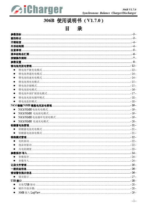
306B 使用说明书 ( V1.7.0 )
目录
参数指标 .........................................................................................................................................................................- 3 能性特点 .........................................................................................................................................................................- 3 开箱检查 .........................................................................................................................................................................- 4 外形结构图 .....................................................................................................................................................................- 4 注意事项 .........................................................................................................................................................................- 5 菜单结构总汇图 ......................................................................................................................- 6 按键操作规则 .................................................................................................................................................................- 7 参数设置 .........................................................................................................................................................................- 8 锂电池充放电管理 .......................................................................................................................................................- 12 -
2MBI100N-120中文资料
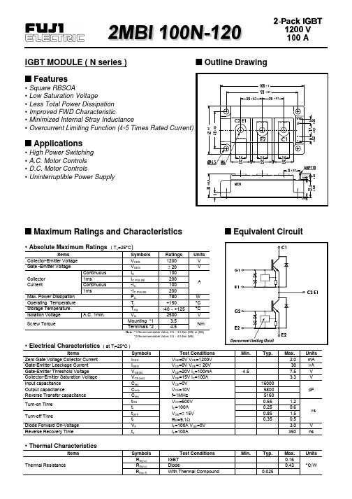
• Absolute Maximum Ratings ( Tc=25°C)
Items
Symbols
Ratings Units
Collector-Emitter Voltage Gate -Emitter Voltage
VCES VGES
1200
V
± 20
V
Collector Current
Max. Power Dissipation Operating Temperature Storage Temperature
Items
Symbols
Zero Gate Voltage Collector Current
ICES
Gate-Emitter Leackage Current
IGES
Gate-Emitter Threshold Voltage
VGE(th)
Collector-Emitter Saturation Voltage
Continuous 1ms Continuous 1ms
IC IC PULSE -IC -IC PULSE PC Tj Tstg
100
200
A
100
200
780
W
+150
°C
-40 ∼ +125 °C
Isolation Voltage Screw Torque
A.C. 1min.
Vis
2500
V
Mounting *1
trr
Test Conditions VGE=0V VCE=1200V VCE=0V VGE=± 20V VGE=20V IC=100mA VGE=15V IC=100A VGE=0V VCE=10V f=1MHz VCC=600V IC=100A VGE=± 15V RG=9.1Ω IF=100A VGE=0V IF=100A
HEDS-9710R-200LPI51资料
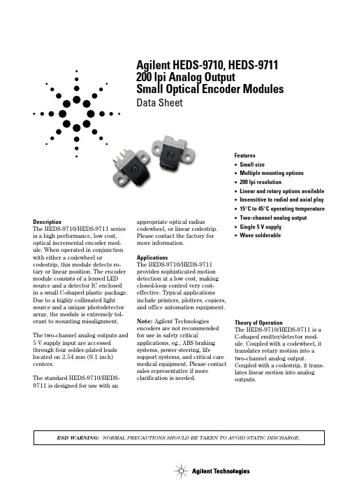
The module contains a single Light Emitting Diode (LED) as its light source. The light is colli-mated into a parallel beam by means of a single lens located directly over the LED. Opposite the emitter is the integrated de-tector circuit. This IC consists of multiple sets of photodetectors and the signal processing cir-cuitry necessary to produce the analog waveforms.The codewheel/codestrip moves between the emitter and detector, causing the light beam to be in-terrupted by the pattern of spaces and bars on the codewheel/ codestrip. The photodiodes which detect these interruptions are arranged in a pattern that corre-sponds to the radius and count density of the codewheel/ codestrip. These detectors are also spaced such that a light period on one pair of detectors corresponds to a dark period on the adjacent pair of detectors. The photodiode outputs are fed through the signal processing circuitry, which produces the final outputs for channels A and B. Due to this integrated phasing technique, the analog output of channel A is in quadrature with channel B (90 degrees out of phase).Package DimensionsSee HEDS-9700 datasheet forpackage outline drawings.DefinitionsCount (N): The number of barand window pairs or Counts PerRevolution (CPR) of the code-wheel, or the number of Lines PerInch (LPI) of the codestrip.1 Shaft Rotation=360 mechanicaldegrees=N cycles1 cycle (c)=360 electricaldegrees (°e)= 1 bar and window pairPulse Width (P): The number ofelectrical degrees that an outputis high during one cycle. Thisvalue is nominally 180°e or 1/2cycle.Pulse Width Error (∆P): Thedeviation, in electrical degrees, ofthe pulse width from its idealvalue of 180°e.State Width (S): The number ofelectrical degrees between atransition in the output of channelA and the neighboring transitionin the output of channel B. Thereare four states per cycle, eachnominally 90°e.State Width Error (∆S): Thedeviation, in electrical degrees, ofeach state width from its idealvalue of 90°e.Phase (Φ): The number of elec-trical degrees between the centerof the high state of channel A andthe center of the high state ofchannel B. This value is nomi-nally 90°e for quadrature output.Phase Error (∆Φ): The devia-tion of the phase from its idealvalue of 90°e.Direction of Rotation: Whenthe codewheel rotates counter-clockwise, as viewed lookingdown on the module (so themarking is visible), channel A willlead channel B. If the codewheelrotates in the opposite direction,channel B will lead channel A.Optical Radius (R OP): Thedistance from the codewheel’scenter of rotation to the opticalcenter (O.C.) of the encodermodule.Mounting Position (R M):Distance from Motor Shaft centerof rotation to center of AlignmentTab receiving hole.Absolute Maximum RatingsParameter Symbol Min.Max.Units Notes Storage Temperature T S–4085°COperating Temperature T A1545°CSupply Voltage V CC–0.57VSoldering Temperature260°C t ≤ 5 sec.Recommended Operating ConditionsParameter Symbol Min.Max.Units Notes Temperature T1545Supply Voltage V CC 4.8 5.2V Ripple < 100 mV p-p Count Frequency8kHz(Velocity (rpm) x N) 60Waveform DefinitionANALOGIap IbpABIamDIGITALABName Paramenter Definition Label Analog Peak The absolute value in µA of the magnitude of the Iap, Ibp,analog signal (i.e., one-sided reading).Iam, Ibm Analog Peak-to-Peak Ipp The peak-to-peak signal magnitude in µA of the Iappanalog signal.Ibpp Analog Offset Ioffset The offset in µA from the mid-point of the analogpeak-to-peak signal to the zero current point.State Width State Width The number of electrical degrees between a transition State 1in channel A and the neighboring transition in channel B.State 2There are four states per cycle, each nominally 90°e.State 3The transitions are determined by where the analog State 4signal crosses the Zero point.State Width Error State Width Error The deviation, in electrical degrees, of each state widthfrom its ideal value of 90°e.Pulse Width Pulse Width The number of electrical degrees that an analog output Pis greater than zero during one cycle. This value isnominally 180°e or 1/2 cycle.Pulse Width Error Pulse Width Error The deviation, in electrical degrees, of each pulse widthfrom its ideal value of 180°e.Electrical CharacteristicsElectrical Characteristics over Recommended Operating Range, Typical at 25°C.Parameter Symbol Min.Typ.Max.Units Notes Supply Current I CC1740mAEncoding CharacteristicsEncoding Characteristics over Recommended Operating Range and Recommended Mounting Tolerances.These characteristics do not include codewheel/codestrip contributions.UnitsRadial microns± 130Tangential microns± 130Gap microns50 – 250 Temperature°C15 – 45O.R.mm18 – LinearCPR count900 – Linear Codewheel Slot/Spoke ratio0.9 – 1.1Min.Max.IppµA1073IoffsetµA–4+4State Width Error e°–40+40Pulse Width Error e°–40+40 Recommended Codewheel and Codestrip CharacteristicsAnalog Encoder Interface CircuitIAIBV REF = 1.4 V ± 0.2 V (DC)The circuit shown can be used to convert the current output to a voltage. Resistor value, R1, and Capacitor, C, are specified to attain required gain and low-pass filtering, which are application specific. The gain is chosen to attain maximum output swing and not clamp the op-amp. V REF should be set to 1.4 V ± 0.2 V.A 0.1 µF bypass capacitor (decoupling capacitor) is recom-mended to be placed within 1 cm of the encoder for optimal power supply noise rejection. Outputs are high impedance (typical 1M ohm) and susceptible to EMI.Ordering Information HEDS-971Lead Configurations0 – straight leads1 – bent leadsResolutionsR – 200 lpiOptionBracket Options5051Package Dimensions Option 50Package Dimensions Option 51FOR DETAILS)C H BV C CC H AG N DLEAD THICKNESS = 0.25 mm LEAD PITCH = 2.54 mmC H BV C CC H AG N DLEAD THICKNESS = 0.25 mm LEAD PITCH = 2.54 mmFOR DETAILS)Package Dimensions Bent Version – Option 50Package Dimensions Bent Version – Option 51LEAD THICKNESS = 0.25 mm LEAD PITCH = 2.54 mmFOR DETAILS)LEAD THICKNESS = 0.25 mm LEAD PITCH = 2.54 mmFOR DETAILS)Mounting ConsiderationsNote: These dimensions include shaft end play and codewheel warp.All dimensions for mounting the module and codewheel/codestrip should be measured with respect to the two mounting posts, shown above.Mounting TolerancesCase 1 specifies the mounting tolerances required on Rm in order to achieve the respective encoding characteristics shown on page 4. The mounting tolerances are as follows:Case 1: Rm ± 0.13 mm (.005 inches)Recommended Screw Size: M2.5 x 0.45 or 2-56/semiconductorsFor product information and a complete list ofdistributors, please go to our web site.For technical assistance call:Americas/Canada: +1 (800) 235-0312 or(408) 654-8675Europe: +49 (0) 6441 92460China: 10800 650 0017Hong Kong: (+65) 6271 2451India, Australia, New Zealand: (+65) 6271 2394Japan: (+81 3) 3335-8152(Domestic/Interna-tional), or 0120-61-1280(Domestic Only)Korea: (+65) 6271 2194Malaysia, Singapore: (+65) 6271 2054Taiwan: (+65) 6271 2654Data subject to change.Copyright © 2002 Agilent Technologies, Inc.Obsoletes 5988-3614ENMay 10, 2002。
M57140-01;中文规格书,Datasheet资料
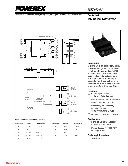
VIN
Direct Current
VO
Between Pins 10 - 9 , 12 - 11, 14 - 13,
IL = 30mA
Between Pins 8 - 7 , IL = 100mA
ILP
Between Pins 10 - 9 , 12 - 11, 14 - 13
Between Pins 8 - 7
Load Regulation Efficiency
Reg-out h
Between Pins 10 - 9 , 12 - 11, 14 - 13, IL = 0 ~ 30mA
Between Pins 8 - 7 , IL = 0 ~ 100mA Between Pins 10 - 9 , 12 - 11, 14 - 13,
IL = 30mA Between Pins 8 - 7 , IL = 100mA
Min. 18 13.5
13.5 – – –
– –
–
Typ. 20 15.0
Max. 22 16.5
Units Volts Volts
15.0 16.5
33
–
110
–
5 10
Volts mA mA %
7 12
%
70
–
%
159 /
Powerex, Inc., 200 Hillis Street, Youngwood, Pennsylvania 15697-1800 (724) 925-7272
M57140-01 Isolated DC-to-DC Converter
Absolute Maximum Ratings, VIN = 20V, Ta = 25 °C unless otherwise specified
TC100B数据手册V1.3中文手册发布
青岛鼎信通讯股份有限公司目录1概述 (1)2功能特点 (1)3原理框图 (1)4引脚定义 (2)4.1 芯片引脚图 (2)4.2 引脚说明 (2)5功能描述 (3)5.1供电电源 (3)5.2过流保护功能 (3)5.3接收发送控制 (3)5.4数据收发 (3)6电气参数 (4)6.1额定直流电气参数 (4)6.2交流电气指标 (5)6.3电气特性图 (5)6.4ESD特性 (6)7封装尺寸 (7)8参考电路 (8)8.1典型应用电路 (8)8.2关键器件选型 (8)1概述XY•CN-PDC总线是一种可供电、无极性、两线制通信机制,具有通讯设备容量大,通讯速率高,设计简单,布线方便,抗干扰能力强等特点。
采用《可供电分布式控制协议XY•CN-PDC》,可保证在252个设备组网情况下,任一设备事件上报时间小于100mS,多点设备同时上报逐一提取,不会产生网络冲突。
XY•CN-PDC总线特别适用于三表集抄、智能家居控制、消防报警及联动控制、楼宇自动化控制等系统。
XY•CN-PDC总线采用主从方式通讯,TC100B芯片实现主站的通讯接口功能,TC001B芯片实现从站的通讯接口功能。
2功能特点静态功耗典型值小于1mA;工作电压范围宽:12V~36V;自带内部稳压输出:+5V,10mA;下行发码满幅电压调制,上行收码电流环解调,抗干扰能力强;最多可挂接252个节点设备;通讯距离1200m,上行通讯速率可达19200bps,下行通讯速率可达9600bps;采用半双工通讯;小体积QFN-16封装;可隔离设计保证电磁兼容特性;功率器件外置,芯片不易损坏;工作温度:-40℃~ +85℃。
3原理框图图1 TC100B原理框图4 引脚定义4.1 芯片引脚图T X DI D E TV O U TTREORXDBUSL GNDV D DV D E T REVINVBBUSHVCCN CR B图2 TC100B 芯片引脚图4.2注:当输入+5V/+3.3V 时,RXD 和EO 输出的高电平为+5V/+3.3V ,低电平为0V 。
英可瑞直流电源模块用户手册
3
4 外形结构与接口
4.1 外形结构
图 1:模块外形图
4.2 输入输出的接口
图 2:航空组件定义图 表 2:整流模块插座定义表 信号名称 交流输入 引脚号 1 2 3 7 8 11 12 15 直流输出 16 18 直流输出正 直流输出负 大地 PE 保护地,请可靠连接。 信号定义 交流输入 A 相 交流输入 B 相 交流输入 C 相 RS485 说 明
2
1 概述
GF22010-10 系列高频开关整流模块先进的 LLC 谐振软开关技术, 效率高;采用无源 PFC 技术,功率因数高;内置完善的 EMC 设计,满足 GB/T 19826-2005 标准中 EMC 相关输入,可以满 足 380VAC 和 415VAC 电网需求。
备
注
≥0.9
/
≥0.9
/
额定输入/额定输出
回缩电流≤40%额定电流,可恢复 300±5VDC,不可恢复 145±3VDC,不可恢复 需手动恢复 交流电压正常后, 自动恢复工作 降温后自动恢复
305±10VAC(恢复电压 317±10VAC) 485±10VAC(恢复电压 468±10VAC) 80℃±5(恢复温度:65℃±5) 温度和电流联合控制,线性调速 88mm×177mm×310mm(宽×高×深) ≤4Kg
2 主要特点
● 输入电压工作范围宽:323VAC~480VAC; ● 采用先进的 LLC 谐振高频软开关技术,效率高,功率密度高; ● 完善的 EMC 设计,满足相关标准要求; ● 内置短路回缩保护,即使模块输出长期处于短路状态也不致损坏; ● 采用 LED 显示,可查询模块的电压、电流、地址及故障信息; ● 完善的保护及告警功能,包括输入过/欠压、输出过压、过温、过流等; ● 风机采用温度联合电流控制调速,噪音小,可靠性高; ● 内置可拆卸式防尘网罩,方便维护; ● 内置防反接保护,支持带电热拔插。
1701Q 1801Q 说明书20100201
小太阳仪器 号位显示比特误码率(BER)值。测量结果如图 2-4 所示。
2.5 伴音载频测量 在频道测量模式下,按动频道键,当前频道的图像载频状态转换为伴 ~12~
MS1701Q/MS1801Q 数字电视场强仪
3、系统设置
3.1 数字参数设置
首先进入数字频道测量模式,如图 3-1。按设置键,仪器进入数字参数
设置状态,显示屏最下方 MODE--表示 QAM 调制方式; BW--表示测量带宽; SR--表示符号率。
显示屏最下方“MODE”闪烁,按数字键输入 6 4 后,按 确认 键。
调制方式有:16QAM,32QAM,64 QAM,128 QAM,256 QAM,一般情况下国内 使用 64 QAM。
~2~
MS1701Q/MS1801Q 数字电视场强仪
1、MS1701Q/MS1801Q 数字电视场强仪一般性说明
1.1 简介 MS1701Q/MS1801Q 数字电视场强仪是专为 CATV 有线电视工程安装检
测人员设计的高性能测量仪器。该仪器采用全数字高亮度宽温液晶显示,读 数清晰准确,由于微处理器的引入,使之功能更强,精度更高,操作更为灵 活方便。 可以很方便地测量 CATV 数字系统的主要技术指标。具有单通道, 双通道,载差测量,载噪比测量,数字平均功率测量,QAM,MER,BER 测 量等强大功能。
1.2 面板装置(见图 1-1/ 1-2)
1、蓄电池充电插口 2、射频输入端子
4、系统设置键
5、功能键
7、数字键
8、充电指示灯
~3~
3、液晶显示屏 6、上,下行调整键 9、电源开关键
