2SB1198中文资料
S-80841CNNB-B82T2G中文资料

Features
• Super-low current consumption • • • • • • 1.3 µA typ. (detection voltage≤1.4 V, at VDD=1.5 V) 0.8 µA typ. (detection voltage≥1.5 V, at VDD=3.5 V) High-precision detection voltage ±2.0% Operating voltage range 0.65 V to 5.0 V (detection voltage≤1.4 V) 0.95 V to 10.0 V (detection voltage≥1.5 V) Hysteresis characteristics 5% typ. Detection voltage 0.8 V to 6.0 V (0.1 V step) Output form Nch open-drain output (Active Low) CMOS output (Active Low) Lead-free products
元器件交易网
Rev.4.3_00
SUPER-SMALL PACKAGE HIGH-PRECISION VOLTAGE DETECTOR
S-808xxC Series
The S-808xxC series is a series of high-precision voltage detectors developed using CMOS process. The detection voltage is fixed internally with an accuracy of ±2.0%. Two output forms, Nch open-drain and CMOS output, are available. Super-low current consumption and miniature package lineup can meet demand from the portable device applications.
2SJ201中文资料

TOSHIBA Field Effect Transistor Silicon P Channel MOS Type2SJ201High-Power Amplifier Applicationz High breakdown voltage: V DSS = −200 V z High forward transfer admittance : |Y fs | = 5.0 S (typ.)z Complementary to 2SK1530Absolute Maximum Ratings (Ta = 25°C)Characteristics Symbol RatingUnitDrain −source voltage V DSS−200 VGate −source voltage V GSS ±20 V Drain current(Note 1)I D−12 A Drain power dissipation (Tc = 25°C) P D 150 W Channel temperature T ch 150 °C Storage temperature rangeT stg−55~150 °CNote: Using continuously under heavy loads (e.g. the application of high temperature/current/voltage and the significant change intemperature, etc.) may cause this product to decrease in the reliability significantly even if the operating conditions (i.e. operating temperature/current/voltage, etc.) are within the absolute maximum ratings. Please design the appropriate reliability upon reviewing the Toshiba Semiconductor Reliability Handbook (“Handling Precautions”/Derating Concept and Methods) and individual reliability data (i.e. reliability test report and estimated failure rate, etc).Unit: mmJEDEC ― JEITA―TOSHIBA 2-21F1B Weight: 9.75 g (typ.)Electrical Characteristics (Ta = 25°C)Characteristics Symbol Test Condition Min Typ. Max UnitDrain cut −off current I DSS V DS = −200 V, V GS = 0 ― ―−1.0mA Gate leakage currentI GSS V DS = 0, V GS = ±20 V ― ― ±0.5μADrain −source breakdown voltageV (BR) DSSI D = −10 mA, V GS = 0−200 ― ― V Gate −source cut −off voltage(Note 2) V GS (OFF) V DS = −10 V, I D = −0.1 A−0.8 ― −2.8V Drain −source saturation voltage V DS (ON)I D = −8 A, V GS = −10 V―−2.0−5.0VForward transfer admittance |Y fs | V DS = −10 V, I D = −5 A ― 5.0 ― S Input capacitance C iss V DS = −30 V, V GS = 0, f = 1 MHz ― 1500 ― Output capacitanceC oss V DS = −30 V, V GS = 0, f = 1 MHz ― 430 ― Reverse transfer capacitanceC rssV DS = −30 V, V GS = 0, f = 1 MHz― 230 ―pFNote 1: Ensure that the channel temperature does not exceed 150°C. Note 2: V GS (OFF) ClassificationO: −0.8~−1.6, Y: −1.4~−2.8This transistor is an electrostatic-sensitive device. Please handle with caution.Markinglead (Pb)-free finish.Switching Time Test Circuit WaveformsRESTRICTIONS ON PRODUCT USE20070701-EN •The information contained herein is subject to change without notice.•TOSHIBA is continually working to improve the quality and reliability of its products. Nevertheless, semiconductor devices in general can malfunction or fail due to their inherent electrical sensitivity and vulnerability to physical stress. It is the responsibility of the buyer, when utilizing TOSHIBA products, to comply with the standards of safety in making a safe design for the entire system, and to avoid situations in which a malfunction or failure of such TOSHIBA products could cause loss of human life, bodily injury or damage to property.In developing your designs, please ensure that TOSHIBA products are used within specified operating ranges as set forth in the most recent TOSHIBA products specifications. Also, please keep in mind the precautions and conditions set forth in the “Handling Guide for Semiconductor Devices,” or “TOSHIBA Semiconductor Reliability Handbook” etc.• The TOSHIBA products listed in this document are intended for usage in general electronics applications (computer, personal equipment, office equipment, measuring equipment, industrial robotics, domestic appliances, etc.).These TOSHIBA products are neither intended nor warranted for usage in equipment that requires extraordinarily high quality and/or reliability or a malfunction or failure of which may cause loss of human life or bodily injury (“Unintended Usage”). Unintended Usage include atomic energy control instruments, airplane or spaceship instruments, transportation instruments, traffic signal instruments, combustion control instruments, medical instruments, all types of safety devices, etc.. Unintended Usage of TOSHIBA products listed in his document shall be made at the customer’s own risk.•The products described in this document shall not be used or embedded to any downstream products of which manufacture, use and/or sale are prohibited under any applicable laws and regulations.• The information contained herein is presented only as a guide for the applications of our products. No responsibility is assumed by TOSHIBA for any infringements of patents or other rights of the third parties which may result from its use. No license is granted by implication or otherwise under any patents or other rights of TOSHIBA or the third parties.• Please contact your sales representative for product-by-product details in this document regarding RoHS compatibility. Please use these products in this document in compliance with all applicable laws and regulations that regulate the inclusion or use of controlled substances. Toshiba assumes no liability for damage or losses occurring as a result of noncompliance with applicable laws and regulations.。
FE2.1中文资料

FE2.1高速七端口USB2.0集线器控制芯片一引言FE2.1芯片是高度集成,高品质,高性能,低能耗,总体花费低的高速七端口USB2.0集线器解决方案。
FE2.1适应多样任务译码器(MMT)风格,借此达到最大的数据输出。
六个(而不是两个)非周期数据处理缓冲器被用来将潜在的传输干扰降至最低。
整个设计基于状态机控制原理,降低了相应延迟时间。
该芯片中没有使用微控制器。
为了保证高品质,整个芯片覆盖测试扫描链—包括高速模块(频率480MHz),所以在运行前可以检测所有逻辑组件。
芯片拥有特殊的自检建立模式,可以在封装和测试阶段测试高速、全速和低速模拟前端结束(AFE)元件。
通过使用0.18微米制造工艺和全面电源/时钟控制机制实现低功耗。
若无必要,芯片的大部分不会被锁住。
特点:■低功耗:□七个下行端口全部在高速模式工作时电流为155mA,□一个下行端口工作在高速模式下电流为66mA,■完全符合通用串行总线规范修订版2.0(USB2.0):□上传端口支持高速度(480MHz信)和全速(12MHZ)模式;□7下行端口支持高速(480MHz信),全速(12MHz)和低速(1.5MHz)模式;。
■集成USB2.0收发器;■集成上传1.5KΩ上拉电阻、下行1.5KΩ下拉电阻和串行电阻;■集成5V转3.3V和1.8V的电压调节器;■集成上电复位电路■集成12MHz的振荡器与反馈电阻和晶体负载电容;■集成12MHz转480MHz锁相回路;■多种任务译码器□一个任务译码器负责一个下行端口;□单任务译码器采用备用接口0,多任务译码器用备用接口1;□每个任务译码器可以处理64个开始分散任务、32个完全分散任务和6个无周期任务;■只支持自供电模式■主板配置选项——□成组或单独的电源控制模式选项;□全局、多模块或单模块过流保护选项;□配置可拆卸或不可拆卸下行设备;□选择下行端口数目;■电可擦可编程只读存储器配置选项——□供应商ID、产品ID和设备发行数量;□可拆卸或不可拆卸下行设备配置;□编号;□下行端口数目:■综合状态指标支持□标准下行端口状态指示灯(每个下行端口有绿色和琥珀色LED控制指示灯);□集线器工作/暂停状态LED指示灯;■支持微软Windows98SE/ME,2000,XP和Vista操作系统;■支持Mac OS 8.6及以上操作系统;■支持Linux 内核2.4.20及以上系统;封装:■64针脚LQFP(大小:10×10mm)■48针脚LQFP (大小: 7×7mm )框图(面积大小:10×10mm)64针脚封装引脚分配图48针脚封装引脚分配图引脚说明表格备注:1.OVCJ[7:2]针脚配有可选择的内部上拉电阻。
2SB系列三极管参数
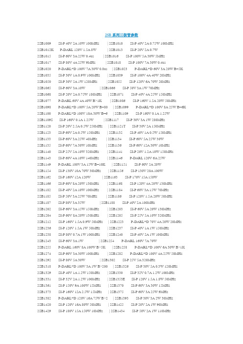
2SB系列三极管参数2SB1009 SI-P 40V 2A 10W 100MHz | 2SB1010 SI-P 40V 2A 0.75W 100MHz2SB1012K P-DARL 120V 1.5A 8W | 2SB1013 SI-P 20V 2A 0.7W2SB1015 SI-P 60V 3A 25W 0.4us | 2SB1016 SI-P 100V 5A 30W 5MHz2SB1017 SI-P 80V 4A 25W 9MHz | 2SB1018 SI-P 100V 7A 30W 0.4us2SB1020 P-DARL+D 100V 7A 30W 0.8us | 2SB1023 P-DARL+D 60V 3A 20W B=5K 2SB1035 SI-P 30V 1A 0.9W 100MHz | 2SB1039 SI-P 100V 4A 40W 20MHz2SB1050 SI-P 30V 5A 1W 120MHz | 2SB1055 SI-P 120V 6A 70W 20MHz2SB1065 SI-P 60V 3A 10W | 2SB1066 SI-P 50V 3A 1W 70MHz2SB1068 SI-P 20V 2A 0.75W 180MHz | 2SB1071 SI-P 40V 4A 25W 150MHz2SB1077 P-DARL 60V 4A 40W B>1K | 2SB1086 SI-P 160V 1.5A 20W 50MHz2SB1098 P-DARL+D 100V 5A 20W B=80 | 2SB1099 P-DARL+D 100V 8A 25W B=6K 2SB1100 P-DARL+D 100V 10A 30W B=6 | 2SB1109 SI-P 160V 0.1A 1.25W2SB1109S SI-P 160V 0.1A 1.25W | 2SB1117 SI-P 30V 3A 1W 280MHz2SB1120 SI-P 20V 2.5A 0.5W 250MHz | 2SB1121T SI-P 30V 2A 150MHz2SB1123 SI-P 60V 2A 0.5W 150MHz | 2SB1132 SI-P 40V 1A 0.5W 150MHz2SB1133 SI-P 60V 3A 25W 40MHz | 2SB1134 SI-P 60V 5A 25W 30W2SB1135 SI-P 60V 7A 30W 10MHz | 2SB1136 SI-P 60V 12A 30W 10MHz2SB1140 SI-P 25V 5A 10W 320MHz | 2SB1141 SI-P 20V 1.2A 10W 150MHz2SB1143 SI-P 60V 4A 10W 140MHz | 2SB1146 P-DARL 120V 6A 25W2SB1149 P-DARL 100V 3A 15W B=10K | 2SB1151 SI-P 60V 5A 20W2SB1154 SI-P 130V 10A 70W 30MHz | 2SB1156 SI-P 130V 20A 100W2SB1162 SI-P 160V 12A 120W | 2SB1163 SI-P 170V 15A 150W2SB1166 SI-P 60V 8A 20W 130MHz | 2SB1168 SI-P 120V 4A 20W 130MHz2SB1182 SI-P 40V 2A 10W 100MHz | 2SB1184 SI-P 60V 3A 15W 70MHz2SB1185 SI-P 50V 3A 25W 70MHz | 2SB1186 SI-P 120V 1.5A 20W 50MHz2SB1187 SI-P 80V 3A 35W | 2SB1188 SI-P 40V 2A 100MHz2SB1202 SI-P 60V 3A 15W 150MHz | 2SB1203 SI-P 60V 5A 20W 130MHz2SB1204 SI-P 60V 8A 20W 130MHz | 2SB1205 SI-P 25V 5A 10W 320MHz2SB1212 SI-P 160V 1.5A 0.9W 50MHz | 2SB1223 P-DARL+D 70V 4A 20W 20MHz2SB1236 SI-P 120V 1.5A 1W 50MHz | 2SB1237 SI-P 40V 1A 1W 150MHz2SB1238 SI-P 80V 0.7A 1W 100MHz | 2SB1240 SI-P 40V 2A 1W 100MHz2SB1243 SI-P 60V 3A 1W | 2SB1254 P-DARL 160V 7A 70W2SB1255 P-DARL 160V 8A 100W B>5K | 2SB1258 P-DARL+D 100V 6A 30W B>1K 2SB1274 SI-P 60V 3A 30W 100MHz | 2SB1282 P-DARL+D 100V 4A 25W 50MHz 2SB1292 SI-P 80V 5A 30W | 2SB1302 SI-P 25V 5A 320MHz2SB1318 P-DARL+D 100V 3A 1W B>200 | 2SB1326 SI-P 30V 5A 0.3W 120MHz2SB1329 SI-P 40V 1A 1.2W 150MHz | 2SB1330 SI-P 32V 0.7A 1.2W 100MHz2SB1331 SI-P 32V 2A 1.2W 100MHz | 2SB1353E SI-P 120V 1.5A 1.8W 50MHz2SB1361 SI-P 150V 9A 100W 15MHz | 2SB1370 SI-P 60V 3A 30W 15MHz2SB1373 SI-P 160V 12A 2.5W 15MHz | 2SB1375 SI-P 60V 3A 25W 9MHz2SB1382 P-DARL+D 120V 16A 75W B>2 | 2SB1393 SI-P 30V 3A 2W 30MHz2SB1420 SI-P 120V 16A 80W 50MHz | 2SB1425 SI-P 20V 2A 1W 90MHz2SB1429 SI-P 180V 15A 150W 10MHz | 2SB1434 SI-P 50V 2A 1W 110MHz2SB1468 SI-P 60/30V 12A 25W | 2SB1470 P-DARL 160V 8A 150W B>5K2SB1490 P-DARL 160V 7A 90W B>5K | 2SB1493 P-DARL 160/140V 7A 70W 20 2SB1503 P-DARL 160V 8A 120W B>5K | 2SB1556 P-DARL 140V 8A 120W B>5K 2SB1557 P-DARL 140V 7A 100W B>5K | 2SB1559 P-DARL 160V 8A 80W B>5K 2SB1560 P-DARL 160V 10A 100W 50MHz | 2SB1565 SI-P 80V 3A 25W 15MHz2SB1587 P-DARL+D 160V 8A 70W B>5K | 2SB1624 P-DARL 110V 6A 60W B>5K 2SB206 GE-P 80V 30A 80W | 2SB324 GE-P 32V 1A 0.25W2SB337 GE-P 50V 7A 30W LF-POWER | 2SB407 GE-P 30V 7A 30W2SB481 GE-P 32V 1A 6W 15KHz | 2SB492 GE-P 25V 2A 6W2SB511E SI-P 35V 1.5A 10W 8MHz | 2SB524 SI-P 60V 1.5A 10W 70MHz2SB527 SI-P 110V 0.8A 10W 70MHz | 2SB531 SI-P 90V 6A 50W 8MHz2SB536 SI-P 130V 1.5A 20W 40MHz | 2SB537 SI-P 130V 1.5A 20W 60MHz2SB541 SI-P 110V 8A 80W 9MHz | 2SB544 SI-P 25V 1A 0.9W 180MHz2SB546A SI-P 200V 2A 25W 5MHz | 2SB549 SI-P 120V 0.8A 10W 80MHz2SB557 SI-P 120V 8A 80W | 2SB560 SI-P 100V 0.7A 0.9W 100MHz2SB561 SI-P 25V 0.7A 0.5W | 2SB564 SI-P 30V 1A 0.8W2SB598 SI-P 25V 1A 0.5W 180MHz | 2SB600 SI-P 200V 15A 200W 4MHz2SB601 P-DARL 100V 5A 30W | 2SB605 SI-P 60V 0.7A 0.8W 120MHz2SB621 SI-N 25V 1.5A 0.6W 200MHz | 2SB621A SI-N 50V 1A 0.75W 200MHz2SB631 SI-P 100V 1A 8W | 2SB632 SI-P 25V 2A 10W 100MHz2SB633 SI-P 100V 6A 40W 15MHz | 2SB637 SI-P 50V 0.1A 0.3W 200MHz2SB641 SI-P 30V 0.1A 120MHz | 2SB647 SI-P 120V 1A 0.9W 140MHz2SB649A SI-P 160V 1.5A 1W 140MHz | 2SB656 SI-P 160V 12A 125W 20MHz2SB673 P-DARL+D 100V 7A 40W 0.8us | 2SB676 P-DARL 100V 4A 30W 0.15us 2SB681 SI-N 150V 12A 100W 13MHz | 2SB688 SI-P 120V 8A 80W 10MHz2SB700 SI-P 160V 12A 100W | 2SB703 SI-P 100V 4A 40W 18MHz2SB705 SI-P 140V 10A 120W 17MHz | 2SB707 SI-P 80V 7A 40W POWER2SB709 SI-P 45V 0.1A 0.2W 80MHz | 2SB716 SI-P 120V 0.05A 0.75W2SB720 SI-P 200V 2A 25W 100MHz | 2SB727 P-DARL+D 120V 6A 50W B>1K 2SB731 SI-P 60V 1A 10W 75MHz | 2SB733 SI-P 20V 2A 1W >50MHz2SB734 SI-P 60V 1A 1W 80MHz | 2SB739 SI-P 20/16V 2A 0.9W 80MHz2SB740 SI-P 70V 1A 0.9W | 2SB744 SI-P 70V 3A 10W 45MHz2SB750 P-DARL+D 60V 2A 35W B>100 | 2SB753 SI-P 100V 7A 40W 0.4us2SB764 SI-P 60V 1A 0.9A 150MHz | 2SB765 P-DARL+D 120V 3A 30W B>1K2SB766 SI-P 30V 1A 200MHz | 2SB772 SI-P 40V 3A 10W 80MHz2SB774 SI-P 30V 0.1A 0.4W 150MHz | 2SB775 SI-P 100V 6A 60W 13MHz2SB776 SI-P 120V 7A 70W 15MHz | 2SB788 SI-P 120V 0.02A 0.4W 150MHz2SB791 P-DARL+D 120V 8A 40W B>10 | 2SB794 P-DARL+D 60V 1.5A 10W B=7 2SB795 P-DARL+D 80V 1.5A 10W B<3 | 2SB808 SI-P 20V 0.7A 0.25W 250MHz 2SB810 SI-P 30V 0.7A 0.35W 160MHz | 2SB815 SI-P 20V 0.7A 0.25W 250MHz2SB816 SI-P 150V 8A 80W 15MHz | 2SB817 SI-P 160V 12A 100W2SB817F SI-P 160V 12A 90W 15MHz | 2SB819 SI-P 50V 1.5A 1W 150MHz2SB822 SI-P 40V 2A 0.75W 100MHz | 2SB824 SI-P 60V 5A 30W 30 MHz2SB825 SI-P 60V 7A 40W 10MHz | 2SB826 SI-P 60V 12A 40W 10MHz2SB827 SI-P 60V 7A 80W 10MHz | 2SB828 SI-P 60V 12A 80W 10MHz2SB829 SI-P 60V 15A 90W 20MHz | 2SB857 SI-P 50V 4A 40W NF/S-L2SB861 SI-P 200V 2A 30W | 2SB863 SI-P 140V 10A 100W 15MHz2SB865 P-DARL 80V 1.5A 0.9W | 2SB873 SI-P 30V 5A 1W 120MHz2SB882 P-DARL+D 70V 10A 40W B>5K | 2SB883 P-DARL+D 70V 15A 70W B=5K 2SB884 P-DARL 110V 3A 30W B=4K | 2SB885 P-DARL+D 110V 3A 35W B=4K 2SB891 SI-P 40V 2A 5W 100MHz | 2SB892 SI-P 60V 2A 1W2SB895A P-DARL 60V 1A B=8000 | 2SB897 P-DARL+D 100V 10A 80W B>12SB908 P-DARL+D 80V 4A 15W 0.15us | 2SB909 SI-P 40V 1A 1W 150MHz2SB922 SI-P 120V 12A 80W 20MHz | 2SB926 SI-P 30V 2A 0.75W2SB938A P-DARL+D 60V 4A 40W B>1K | 2SB940 SI-P 200V 2A 35W 30MHz2SB941 SI-P 60V 3A 35W POWER | 2SB945 SI-P 130V 5A 40W 30MHz2SB946 SI-P 130V 7A 40W 30MHz | 2SB950A P-DARL+D 80V 4A 40W B>1K2SB953A SI-P 50V 7A 30W 150MHz | 2SB955 P-DARL+D 120V 10A 50W B=42SB975 P-DARL+D 100V 8A 40W B>6K | 2SB976 SI-P 27V 5A 0.75W 120MHz2SB985 SI-P 60V 3A 1W 150MHz | 2SB986 SI-P 60V 4A 10W 150MHz2SB988 SI-P 60V 3A 30W <400/2200。
东芝芯片资料
0 900Ω 600Ω 19.5K 15K 13K 19K
LA7833引脚功能
引脚
1 2 3 4 4 6 7
功能
接地端 场输出 自举升压电源端 场激励输入 负反馈输入及相位补偿 电源端 场逆程脉冲输出
直流电压
0V 13.6V 25.5V 0.8V 0.8V 26V 1.4V
纹波滤波电路引脚 第二伴音中频输出 调频直流反馈滤波电路引脚
电压
1.8V 0V 1.3V
+2.5V
+5V 2.45V 2.45V
1V 6.4V 0V 0V 2.3V 1.6V 0V +5V 3.6V 4.3V 0V 8V 8.8V 3.5V 5.6V 3.4V 3.5V
RXIK档对地电阻(黑表笔接地)
场AGC 总线时钟端子 总线数据端子
行电源 SECAM识别/载波信号输出
行逆程脉冲输入 复合同步信号输出 行激励信号输出
接地 沙堡脉冲输出 视频信号输出
数字电源
SECAM蓝色差信号输入 SECAM红色差信号输入
亮度信号输入 行AFC滤波
外接视频信号
接地 视频信Leabharlann 输入黑电平检测滤波直流电压(V)
有信号 4.9
800Ω 0
12.5K
12.8K
6K 13K 13K 13K 12.8K 13.2K
0 12.8K 13K 11.5K
1K 12.5K 12K
0 900Ω 600Ω 12.5K 12.2K 11.5K 12K
红笔接地 R×1K档
800Ω 0
19K
27K
5.5K 20K 20K 18K 28K 28K
2SK2608中文资料

TOSHIBA Field Effect Transistor Silicon N Channel MOS Type (π−MOSIII)2SK2608Switching Regulator Applicationsz Low drain −source ON resistance : R DS (ON) = 3.73 Ω (typ.) z High forward transfer admittance : |Y fs |= 2.6 S (typ.)z Low leakage current : I DSS = 100 μA (max) (V DS = 720 V) z Enhancement mode : V th = 2.0~4.0 V (V DS = 10 V, I D = 1 mA)Absolute Maximum Ratings (Ta = 25°C)Characteristics Symbol Rating UnitDrain −source voltageV DSS 900 VDrain −gate voltage (R GS = 20 k Ω) V DGR 900 V Gate −source voltage V GSS ±30 V DC (Note 1) I D 3 A Drain currentPulse (Note 1)I DP 9A Drain power dissipation (Tc = 25°C)P D 100 WSingle pulse avalanche energy(Note 2) E AS 295mJ Avalanche currentI AR 3 ARepetitive avalanche energy (Note 3) E AR 10.0 mJ Channel temperature T ch 150 °C Storage temperature rangeT stg−55~150 °CNote: Using continuously under heavy loads (e.g. the application of high temperature/current/voltage and the significant change intemperature, etc.) may cause this product to decrease in the reliability significantly even if the operating conditions (i.e. operating temperature/current/voltage, etc.) are within the absolute maximum ratings. Please design the appropriate reliability upon reviewing the Toshiba Semiconductor Reliability Handbook (“Handling Precautions”/Derating Concept and Methods) and individual reliability data (i.e. reliability test report and estimated failure rate, etc).Thermal CharacteristicsCharacteristics Symbol Max UnitThermal resistance, channel to case R th (ch −c) 1.25 °C / W Thermal resistance, channel to ambientR th (ch −a)83.3°C / WNote 1: Ensure that the channel temperature does not exceed 150°C. Note 2: V DD = 90 V, T ch = 25°C (initial), L = 60.0 mH, R G = 25 Ω, I AR = 3 A Note 3: Repetitive rating: pulse width limited by maximum channel temperature This transistor is an electrostatic-sensitive device. Please handle with caution.Unit: mmJEDEC TO-220AB JEITA SC-46 TOSHIBA 2-10P1B Weight: 2.0 g (typ.)Electrical Characteristics (Ta = 25°C)Characteristics SymbolTest ConditionMin Typ. Max Unit Gate leakage currentI GSS V GS = ±30 V, V DS = 0 V — — ±10μA Gate −source breakdown voltage V (BR) GSS I G = ±10 μA, V DS = 0 V ±30 — — V Drain cut −off currentI DSS V DS = 720 V, V GS = 0 V — — 100μA Drain −source breakdown voltage V (BR) DSS I D = 10 mA, V GS = 0 V 900 — — V Gate threshold voltage V th V DS = 10 V, I D = 1 mA 2.0 — 4.0 V Drain −source ON resistance R DS (ON)V GS = 10 V, I D = 1.5 A— 3.73 4.3 Ω Forward transfer admittance |Y fs | V DS = 20 V, I D = 1.5 A0.652.6—SInput capacitanceC iss — 750 —Reverse transfer capacitance C rss — 10 — Output capacitanceC ossV DS = 25 V, V GS = 0 V, f = 1 MHz — 70 —pF Rise timet r — 15 —Turn −on timet on — 55 —Fall timet f — 30 — Switching timeTurn −off timet off— 110 —nsTotal gate charge (gate −sourceplus gate −drain) Q g —25 — Gate −source charge Q gs — 13 — Gate −drain (“miller”) ChargeQ gdV DD ≈ 400 V, V GS = 10 V, I D = 3 A — 12 —nCSource −Drain Ratings and Characteristics (Ta = 25°C)Characteristics SymbolTest ConditionMin Typ. Max UnitContinuous drain reverse current(Note 1)I DR —— — 3 A Pulse drain reverse current(Note 1) I DRP —— — 9 A Forward voltage (diode) V DSF I DR = 3 A, V GS = 0 V——−1.9VReverse recovery time t rr — 1200 — ns Reverse recovery chargeQ rrI DR = 3 A, V GS = 0 V, dI DR / dt = 100 A / μs— 8.5 — μCMarkinglead (Pb)-free package or lead (Pb)-free finish.K2608⎟⎠⎞⎜⎝⎛−⋅⋅⋅=DD VDSS VDSS AS V B B I L 21E 2R G = 25 ΩV DD = 90 V , L = 60 mHRESTRICTIONS ON PRODUCT USE20070701-EN •The information contained herein is subject to change without notice.•TOSHIBA is continually working to improve the quality and reliability of its products. Nevertheless, semiconductor devices in general can malfunction or fail due to their inherent electrical sensitivity and vulnerability to physical stress. It is the responsibility of the buyer, when utilizing TOSHIBA products, to comply with the standards of safety in making a safe design for the entire system, and to avoid situations in which a malfunction or failure of such TOSHIBA products could cause loss of human life, bodily injury or damage to property.In developing your designs, please ensure that TOSHIBA products are used within specified operating ranges as set forth in the most recent TOSHIBA products specifications. Also, please keep in mind the precautions and conditions set forth in the “Handling Guide for Semiconductor Devices,” or “TOSHIBA Semiconductor Reliability Handbook” etc.• The TOSHIBA products listed in this document are intended for usage in general electronics applications (computer, personal equipment, office equipment, measuring equipment, industrial robotics, domestic appliances, etc.).These TOSHIBA products are neither intended nor warranted for usage in equipment that requires extraordinarily high quality and/or reliability or a malfunction or failure of which may cause loss of human life or bodily injury (“Unintended Usage”). Unintended Usage include atomic energy control instruments, airplane or spaceship instruments, transportation instruments, traffic signal instruments, combustion control instruments, medical instruments, all types of safety devices, etc.. Unintended Usage of TOSHIBA products listed in his document shall be made at the customer’s own risk.•The products described in this document shall not be used or embedded to any downstream products of which manufacture, use and/or sale are prohibited under any applicable laws and regulations.• The information contained herein is presented only as a guide for the applications of our products. No responsibility is assumed by TOSHIBA for any infringements of patents or other rights of the third parties which may result from its use. No license is granted by implication or otherwise under any patents or other rights of TOSHIBA or the third parties.• Please contact your sales representative for product-by-product details in this document regarding RoHS compatibility. Please use these products in this document in compliance with all applicable laws and regulations that regulate the inclusion or use of controlled substances. Toshiba assumes no liability for damage or losses occurring as a result of noncompliance with applicable laws and regulations.。
2SB1375中文资料
Ta = 25°C Tc = 25°C
Junction temperature
Storage temperature range
VCBO VCEO VEBO
IC IB
PC
Tj Tstg
−60
V
−60
V
−7
V
−3
A
−0.5
A
2.0 W
25
150
°C
−55 to 150
°C
JEDEC
―
JEITA
―
TOSHIBA
2-10R1A
Weight: 1.7 g (typ.)
Note: Using continuously under heavy loads (e.g. the application of high temperature/current/voltage and the significant change in temperature, etc.) may cause this product to decrease in the reliability significantly even if the operating conditions (i.e. operating temperature/current/voltage, etc.) are within the absolute maximum ratings. Please design the appropriate reliability upon reviewing the Toshiba Semiconductor Reliability Handbook (“Handling Precautions”/Derating Concept and Methods) and individual reliability data (i.e. reliability test report and estimated failure rate, etc).
2SB1079中文资料

2SB1079Silicon PNP Triple DiffusedApplicationLow frequency power amplifier complementary pair with 2SD1559 Outline2SB10792Absolute Maximum Ratings (Ta = 25°C)ItemSymbol Ratings Unit Collector to base voltage V CBO –100V Collector to emitter voltage V CEO –100V Emitter to base voltage V EBO –7V Collector current I C –20A Collector peak current I C(peak)–30A Base currentI B –3A Collector power dissipation P C *1100W Junction temperature Tj 150°C Storage temperature Tstg–55 to +150°CNote:1.Value at T C = 25°C.Electrical Characteristics (Ta = 25°C)ItemSymbol Min Typ Max Unit Test conditions Collector to base breakdown voltageV (BR)CBO–100——V I C = –0.1 mA, I E = 0Collector to emitter breakdown voltageV (BRCEO –100——V I C = –25 mA, R BE = ∞Collector to emitter sustain voltageV CEO(sus)–100——V I C = –200 mA, R BE = ∞*1Emitter to base breakdown voltageV (BR)EBO –7——V I E = –50 mA, I C = 0Collector cutoff current I CBO ——–100µA V CB = –100 V, I E = 0I CEO ——–1.0mAV CE = –80 V, R BE = ∞DC current transfer ratio h FE 1000—20000V CE = –3 V, I C = –10 A*1Collector to emitter saturation voltageV CE(sat)1——–2.0V I C = –10 A, I B = –20 mA*1Base to emitter saturation voltageV BE(sat)1——–2.5V Collector to emitter saturation voltageV CE(sat)2——–3.0V I C = –20 A, I B = –200 mA*1Base to emitter saturation voltage V BE(sat)2——–3.5V Turn on time t on —0.6—µs I C = –10 A, I B1 = –I B2 = –20 mA Storage time t stg—3.5—µsNote:1.Pulse Test.2SB107932SB10794Hitachi CodeJEDECEIAJWeight (reference value)TO-3P—Conforms5.0 gUnit: mmCautions1.Hitachi neither warrants nor grants licenses of any rights of Hitachi’s or any third party’s patent,copyright, trademark, or other intellectual property rights for information contained in this document.Hitachi bears no responsibility for problems that may arise with third party’s rights, includingintellectual property rights, in connection with use of the information contained in this document.2.Products and product specifications may be subject to change without notice. Confirm that you have received the latest product standards or specifications before final design, purchase or use.3.Hitachi makes every attempt to ensure that its products are of high quality and reliability. However,contact Hitachi’s sales office before using the product in an application that demands especially high quality and reliability or where its failure or malfunction may directly threaten human life or cause risk of bodily injury, such as aerospace, aeronautics, nuclear power, combustion control, transportation,traffic, safety equipment or medical equipment for life support.4.Design your application so that the product is used within the ranges guaranteed by Hitachi particularly for maximum rating, operating supply voltage range, heat radiation characteristics, installationconditions and other characteristics. Hitachi bears no responsibility for failure or damage when used beyond the guaranteed ranges. Even within the guaranteed ranges, consider normally foreseeable failure rates or failure modes in semiconductor devices and employ systemic measures such as fail-safes, so that the equipment incorporating Hitachi product does not cause bodily injury, fire or other consequential damage due to operation of the Hitachi product.5.This product is not designed to be radiation resistant.6.No one is permitted to reproduce or duplicate, in any form, the whole or part of this document without written approval from Hitachi.7.Contact Hitachi’s sales office for any questions regarding this document or Hitachi semiconductor products.Hitachi, Ltd.Semiconductor & Integrated Circuits.Nippon Bldg., 2-6-2, Ohte-machi, Chiyoda-ku, Tokyo 100-0004, Japan Tel: Tokyo (03) 3270-2111 Fax: (03) 3270-5109Copyright ' Hitachi, Ltd., 1999. All rights reserved. Printed in Japan.Hitachi Asia Pte. Ltd.16 Collyer Quay #20-00Hitachi TowerSingapore 049318Tel: 535-2100Fax: 535-1533URLNorthAmerica : http:/Europe : /hel/ecg Asia (Singapore): .sg/grp3/sicd/index.htm Asia (Taiwan): /E/Product/SICD_Frame.htm Asia (HongKong): /eng/bo/grp3/index.htm Japan : http://www.hitachi.co.jp/Sicd/indx.htmHitachi Asia Ltd.Taipei Branch Office3F, Hung Kuo Building. No.167, Tun-Hwa North Road, Taipei (105)Tel: <886> (2) 2718-3666Fax: <886> (2) 2718-8180Hitachi Asia (Hong Kong) Ltd.Group III (Electronic Components)7/F., North Tower, World Finance Centre,Harbour City, Canton Road, Tsim Sha Tsui,Kowloon, Hong Kong Tel: <852> (2) 735 9218Fax: <852> (2) 730 0281 Telex: 40815 HITEC HXHitachi Europe Ltd.Electronic Components Group.Whitebrook ParkLower Cookham Road MaidenheadBerkshire SL6 8YA, United Kingdom Tel: <44> (1628) 585000Fax: <44> (1628) 778322Hitachi Europe GmbHElectronic components Group Dornacher Stra§e 3D-85622 Feldkirchen, Munich GermanyTel: <49> (89) 9 9180-0Fax: <49> (89) 9 29 30 00Hitachi Semiconductor (America) Inc.179 East Tasman Drive,San Jose,CA 95134 Tel: <1> (408) 433-1990Fax: <1>(408) 433-0223For further information write to:。
2SK2082-01中文资料
- Electrical Characteristics (TC=25°C), unless otherwise specified
Item
Symbol
Test conditions
Drain-Source Breakdown-Voltage
V (BR)DSS ID=1mA
VGS=0V
Gate Threshhold Voltage
V GS(th)
ID=1mA
VDS=VGS
Zero Gate Voltage Drain Current
I DSS
VDS=900V Tch=25°C
VGS=0V
Tch=125°C
Gate Source Leakage Current
I GSS
11
ID [A]
PD [W]
→ Tc [°C]
→ VDS [V]
This specification is subject to change without notice!
t [s] →
1,1 1,4 Ω
5
10
S
2200 3300 pF
210 320 pF
65 100 pF
25
40 ns
60
90 ns
140 210 ns
70 110 ns
9
A
9A
36 A
1,2 1,8 V
450
ns
4
µC
- Thermal Characteristics Item Thermal Resistance
tf
RGS=10 Ω
Avalanche Capability
2SK3318中文资料

40 55 310 70
Note) Measuring methods are based on JAPANESE INDUSTRIAL STANDARD JIS C 7030 measuring methods for transistors.
Publication date: November 2004 SJG00040AED
(1) An export permit needs to be obtained from the competent authorities of the Japanese Government if any of the products or technical information described in this material and controlled under the "Foreign Exchange and Foreign Trade Law" is to be exported or taken out of Japan. (2) The technical information described in this material is limited to showing representative characteristics and applied circuits examples of the products. It neither warrants non-infringement of intellectual property right or any other rights owned by our company or a third party, nor grants any license. (3) We are not liable for the infringement of rights owned by a third party arising out of the use of the technical information as described in this material. (4) The products described in this material are intended to be used for standard applications or general electronic equipment (such as office equipment, communications equipment, measuring instruments and household appliances). Consult our sales staff in advance for information on the following applications: • Special applications (such as for airplanes, aerospace, automobiles, traffic control equipment, combustion equipment, life support systems and safety devices) in which exceptional quality and reliability are required, or if the failure or malfunction of the products may directly jeopardize life or harm the human body. • Any applications other than the standard applications intended. (5) The products and product specifications described in this material are subject to change without notice for modification and/or improvement. At the final stage of your design, purchasing, or use of the products, therefore, ask for the most up-to-date Product Standards in advance to make sure that the latest specifications satisfy your requirements. (6) When designing your equipment, comply with the guaranteed values, in particular those of maximum rating, the range of operating power supply voltage, and heat radiation characteristics. Otherwise, we will not be liable for any defect which may arise later in your equipment. Even when the products are used within the guaranteed values, take into the consideration of incidence of break down and failure mode, possible to occur to semiconductor products. Measures on the systems such as redundant design, arresting the spread of fire or preventing glitch are recommended in order to prevent physical injury, fire, social damages, for example, by using the products. (7) When using products for which damp-proof packing is required, observe the conditions (including shelf life and amount of time let standing of unsealed items) agreed upon when specification sheets are individually exchanged. (8) This material may be not reprinted or reproduced whether wholly or partially, without the prior written permission of Matsushita Electric Industrial Co., Ltd.
BK1198数据手册v1.2 New
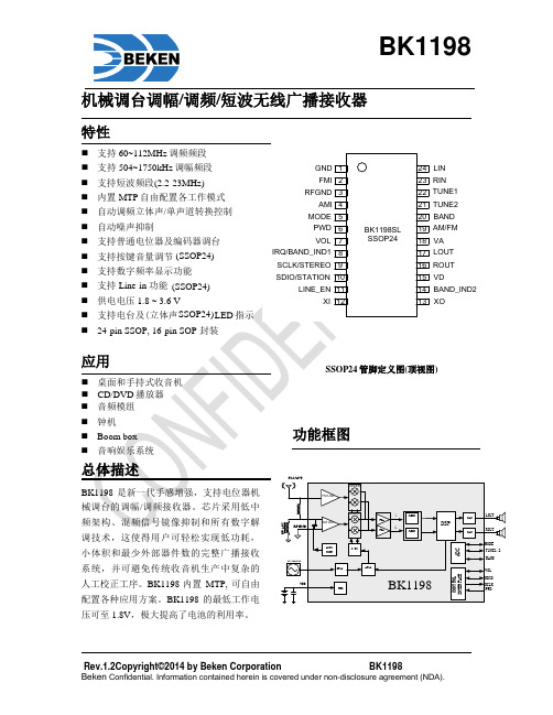
REG
BK1198
ADC
LOUT
DAC
DAC
ROUT
MODE TUNE1/2
BAND
VOL
SDIO SCLK PWD
CONTROL INTERFACE
图 1BK1198 功能框图
2.1 调频接收器
FM接收器采用了可减少外围器件数量 的数字低中频架构,内部集成了支持 全世界调频广播频段(60-112MHz) 的低噪声放大器(LNA),可以控制 LNA的增益从而优化灵敏度和抑制大 干扰信号的自动增益控制器(AGC), 可把射频信号转换为低中频信号的镜 像抑制混频器。混频器的输出通过一 个可编程增益控制放大器(PGA)来 放大,然后由一个高分辨率的模数转 换器(ADC)转换成数字信号。一个 音频数字信号处理器(DSP)完成了 频道选择、FM解调、立体声多路解码 器和输出音频信号的功能。多路解码 器可自动从立体声转换成单声道解码, 从而限制了输出噪声。
2.2 中波接收器
BK1198通过3个波段可支持全世界调 幅频段(504-1750kHz)。它使用了低 中频架构从而使外围器件的数量达到 最小数量。使用这种架构可实现高精 度的滤波,从而达到了极好的灵敏度 和噪声抑制。同FM接收器相似,AM 接收器集成了LNA和AGC,这优化了 灵敏度抑制了大干扰信号,从而使得 弱信号电台也能够有良好的接收效果。 BK1198提供了高准确度的数字AM自 动调谐,从而省去了产线调试。为了 最大限度地提供灵活性,对于中波频 段,接收器可以支持180~300µH范围 的磁棒线圈。
MW ANT
SSOP24 管脚定义图(顶视图)
功能框图
FM ANT
RFGND
32.768KHz
VDD
FM LNA
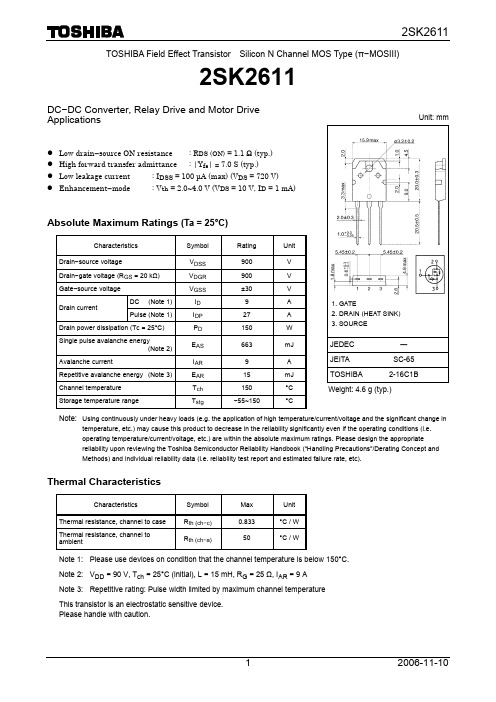
2SK2611中文资料
TOSHIBA Field Effect Transistor Silicon N Channel MOS Type (π−MOSIII)2SK2611DC −DC Converter, Relay Drive and Motor Drive Applicationsz Low drain −source ON resistance : R DS (ON) = 1.1 Ω (typ.) z High forward transfer admittance : |Y fs | = 7.0 S (typ.)z Low leakage current : I DSS = 100 μA (max) (V DS = 720 V)z Enhancement −mode : V th = 2.0~4.0 V (V DS = 10 V, I D = 1 mA)Absolute Maximum Ratings (Ta = 25°C)Characteristics Symbol Rating UnitDrain −source voltageV DSS 900 VDrain −gate voltage (R GS = 20 k Ω) V DGR 900 VGate −source voltage V GSS ±30 VDC (Note 1) I D 9 A Drain currentPulse (Note 1)I DP 27A Drain power dissipation (Tc = 25°C)P D 150 WSingle pulse avalanche energy(Note 2) E AS 663mJ Avalanche currentI AR 9 A Repetitive avalanche energy (Note 3) E AR 15 mJChannel temperature T ch 150 °C Storage temperature rangeT stg−55~150 °CNote: Using continuously under heavy loads (e.g. the application of high temperature/current/voltage and the significant change intemperature, etc.) may cause this product to decrease in the reliability significantly even if the operating conditions (i.e. operating temperature/current/voltage, etc.) are within the absolute maximum ratings. Please design the appropriate reliability upon reviewing the Toshiba Semiconductor Reliability Handbook (“Handling Precautions”/Derating Concept and Methods) and individual reliability data (i.e. reliability test report and estimated failure rate, etc).Thermal CharacteristicsCharacteristics Symbol Max UnitThermal resistance, channel to case R th (ch −c) 0.833 °C / W Thermal resistance, channel to ambientR th (ch −a)50°C / WNote 1: Please use devices on condition that the channel temperature is below 150°C. Note 2: V DD = 90 V, T ch = 25°C (initial), L = 15 mH, R G = 25 Ω, I AR = 9 A Note 3: Repetitive rating: Pulse width limited by maximum channel temperature This transistor is an electrostatic sensitive device. Please handle with caution.Unit: mm1. GATE2. DRAIN (HEAT SINK)3. SOURCEJEDEC ―JEITA SC-65 TOSHIBA 2-16C1B Weight: 4.6 g (typ.)Electrical Characteristics (Ta = 25°C)Characteristics SymbolTest ConditionMin Typ. Max Unit Gate leakage currentI GSS V GS = ±30 V, V DS = 0 V — — ±10μA Gate −source breakdown voltage V (BR) GSS I G = ±10 μA, V DS = 0 V ±30 — — V Drain cut −off currentI DSS V DS = 720 V, V GS = 0 V — — 100μA Drain −source breakdown voltage V (BR) DSS I D = 10 mA, V GS = 0 V 900 — — V Gate threshold voltage V th V DS = 10 V, I D = 1 mA 2.0 — 4.0 V Drain −source ON resistance R DS (ON)V GS = 10 V, I D = 4 A— 1.11.4ΩForward transfer admittance |Y fs | V DS = 15 V, I D = 4 A3.07.0 — SInput capacitanceC iss — 2040 —Reverse transfer capacitance C rss — 45 — Output capacitanceC ossV DS = 25 V, V GS = 0 V, f = 1 MHz — 190 —pF Rise timet r — 25 —Turn −on timet on — 60 —Fall timet f — 20 —Switching timeTurn −off timet off— 95 —nsTotal gate charge (gate −sourceplus gate −drain) Q g —58 — Gate −source charge Q gs — 32 — Gate −drain (“miller”) ChargeQ gdV DD ≈ 400 V, V GS = 10 V, I D = 9 A — 26 —nCSource −Drain Ratings and Characteristics (Ta = 25°C)Characteristics SymbolTest ConditionMin Typ. Max UnitContinuous drain reverse current(Note 1)I DR —— — 9 A Pulse drain reverse current(Note 1) I DRP —— — 27 A Forward voltage (diode) V DSF I DR = 9 A, V GS = 0 V——−1.9VReverse recovery time t rr — 1.6 — μs Reverse recovery chargeQ rrI DR = 9 A, V GS = 0 V, dI DR / dt = 100 A / μs— 20 — μCMarkinglead (Pb)-free package or lead (Pb)-free finish.⎟⎠⎞⎜⎝⎛−⋅⋅⋅=DD VDSS VDSS AS V B B I L 21E 2R G = 25 ΩV DD = 90 V , L = 15 mHRESTRICTIONS ON PRODUCT USE20070701-EN •The information contained herein is subject to change without notice.•TOSHIBA is continually working to improve the quality and reliability of its products. Nevertheless, semiconductor devices in general can malfunction or fail due to their inherent electrical sensitivity and vulnerability to physical stress. It is the responsibility of the buyer, when utilizing TOSHIBA products, to comply with the standards of safety in making a safe design for the entire system, and to avoid situations in which a malfunction or failure of such TOSHIBA products could cause loss of human life, bodily injury or damage to property.In developing your designs, please ensure that TOSHIBA products are used within specified operating ranges as set forth in the most recent TOSHIBA products specifications. Also, please keep in mind the precautions and conditions set forth in the “Handling Guide for Semiconductor Devices,” or “TOSHIBA Semiconductor Reliability Handbook” etc.• The TOSHIBA products listed in this document are intended for usage in general electronics applications (computer, personal equipment, office equipment, measuring equipment, industrial robotics, domestic appliances, etc.).These TOSHIBA products are neither intended nor warranted for usage in equipment that requires extraordinarily high quality and/or reliability or a malfunction or failure of which may cause loss of human life or bodily injury (“Unintended Usage”). Unintended Usage include atomic energy control instruments, airplane or spaceship instruments, transportation instruments, traffic signal instruments, combustion control instruments, medical instruments, all types of safety devices, etc.. Unintended Usage of TOSHIBA products listed in his document shall be made at the customer’s own risk.•The products described in this document shall not be used or embedded to any downstream products of which manufacture, use and/or sale are prohibited under any applicable laws and regulations.• The information contained herein is presented only as a guide for the applications of our products. No responsibility is assumed by TOSHIBA for any infringements of patents or other rights of the third parties which may result from its use. No license is granted by implication or otherwise under any patents or other rights of TOSHIBA or the third parties.• Please contact your sales representative for product-by-product details in this document regarding RoHS compatibility. Please use these products in this document in compliance with all applicable laws and regulations that regulate the inclusion or use of controlled substances. Toshiba assumes no liability for damage or losses occurring as a result of noncompliance with applicable laws and regulations.。
BAS321中文资料

MAM406
Fig.1 Simplified outline (SOD323) and symbol.
LIMITING VALUES In accordance with the Absolute Maximum Rating System (IEC 60134). SYMBOL VRRM VR IF IFRM IFSM PARAMETER repetitive peak reverse voltage continuous reverse voltage continuous forward current repetitive peak forward current non-repetitive peak forward current see Fig.2; note 1 tp < 0.5 ms; δ ≤ 0.25 square wave; Tj = 25 °C prior to surge; see Fig.4 t = 1 µs t = 100 µs t = 10 ms Ptot Tstg Tj Note 1. Device mounted on an FR4 printed circuit-board. total power dissipation storage temperature junction temperature Tamb = 25 °C; note 1 − − − − −65 − 9 3 1.7 300 +150 150 A A A mW °C °C CONDITIONS − − − − MIN. MAX. 250 200 250 625 V V mA mA UNIT