MSP中文数据手册
MSP中文资料
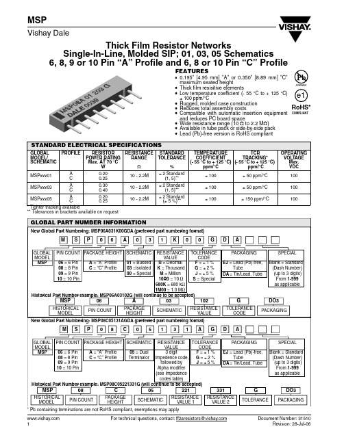
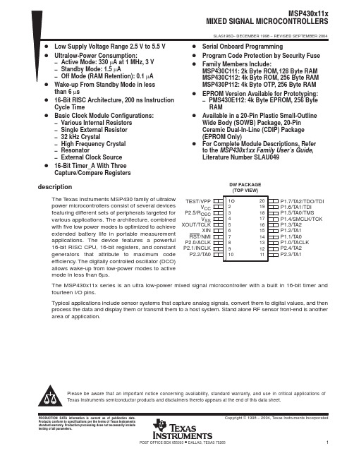
Thick Film Resistor NetworksSingle-In-Line, Molded SIP; 01, 03, 05 Schematics 6, 8, 9 or 10 Pin “A” Profile and 6, 8 or 10 Pin “C” ProfileFor technical questions, contact: ff2aresistors@Document Number: 31510MSPVishay DaleFEATURES•0.195" [4.95 mm] "A" or 0.350" [8.89 mm] "C"maximum seated height•Thick film resisitive elements•Low temperature coefficient (- 55 °C to + 125 °C)± 100 ppm/°C•Rugged, molded case construction •Reduces total assembly costs•Compatible with automatic insertion equipment and reduces PC board space•Wide resistance range (10 Ω to 2.2 M Ω)•Available in tube pack or side-by-side pack •Lead (Pb)-free version is RoHS compliant* Tighter tracking available** Tolerances in brackets available on requestSTANDARD ELECTRICAL SPECIFICATIONSGLOBAL MODEL/ SCHEMATICPROFILE RESISTOR POWER RATING Max. AT 70 °CW RESISTANCE RANGE ΩSTANDARD TOLERANCE%TEMPERATURE COEFFICIENT (- 55 °C to + 125 °C)ppm/°C TCR TRACKING* (- 55 °C to + 125 °C)ppm/°COPERATINGVOLTAGE Max. VDCMSPxxx01A C 0.20 0.25 10 - 2.2M ± 2 Standard (1, 5)** ± 100 ± 50 ppm/°C 100 MSPxxx03 A C0.30 0.4010 - 2.2M ± 2 Standard (1, 5)** ± 100 ± 50 ppm/°C 100 MSPxxx05A C 0.20 0.2510 - 2.2M± 2 Standard (± 5 %)**± 100± 150 ppm/°C100Document Number: 31510For technical questions, contact: ff2aresistors@MSPThick Film Resistor Networks Single-In-Line, Molded SIP;01, 03, 05 Schematics 6, 8, 9 or 10 Pin "A" Profileand 6, 8 or 10 Pin "C" ProfileVishay DaleDIMENSIONSin inches [millimeters]GLOBAL MODEL A (Max.)B C D (Max.)MSP060.590 [14.99]0.500 [12.70]5MSPxxA = 0.195 [4.95]MSPxxC = 0.350 [8.89]MSP080.790 [20.07]0.700 [17.78]7MSP100.990 [25.15]0.900 [22.86]9MSP090.890 [22.61]0.800 [20.32]80.195 [4.95] ONL YTECCHNICAL SPECIFICATIONSPARAMETERUNITMSP SERIES Package Power RatingMaximum at + 25 °C and + 70 °C See Derating Curves Voltage Coefficient of Resistance V eff < 50 ppm typicalDielectric StrengthVAC 200Isolation Resistance (03 Schematic)Ω> 100M Operating T emperature Range °C - 55 to + 125Storage T emperature Range°C - 55 to + 150MECHANICAL SPECIFICATIONSMarking Resistance to Solvents:Permanency testing per MIL-STD-202, Method 215Solderability:Per MIL-STD-202, Method 208E, RMA flux Body:Molded epoxyT erminals:Copper alloy, solder plated Weight:MSP06A = 0.4 gram MSP06C = 0.7 gram MSP08A = 0.5 gram MSP08C = 0.9 gram MSP09A = 0.55 gram MSP10C = 1.1 gramMSP10A = 0.6 gram For technical questions, contact: ff2aresistors@Document Number: 31510MSPVishay DaleThick Film Resistor Networks Single-In-Line, Molded SIP;01, 03, 05 Schematics 6, 8, 9 or 10 Pin "A" Profileand 6, 8 or 10 Pin "C" ProfileIMPEDANCE CODESCODE R 1(Ω) R 2(Ω)CODE R 1(Ω) R 2(Ω)500B 82130141A 270270750B 120200181A 330390800C 130210191A 330470990A 160260221B 330680101C 180240281B 560560111C 180270381B 560 1.2K 121B 180390501C 620 2.7K 121C 220270102A 1.5K 3.3K 131A220330202B3K6.2KMSPThick Film Resistor Networks Single-In-Line, Molded SIP;01, 03, 05 Schematics 6, 8, 9 or 10 Pin "A" Profileand 6, 8 or 10 Pin "C" ProfileVishay DaleDocument Number: 31510For technical questions, contact: ff2aresistors@Higher power ratings available. Contact factory."A" PROFILE + 70 °C PACKAGE RATINGSMSP10A 1.25 watts MSP09A 1.12 watts MSP08A 1.00 watts MSP06A0.75 watts"C" PROFILE + 70 °C PACKAGE RATINGSMSP10C 1.60 watts MSP08C 1.30 watts MSP06C1.00 wattsPERFORMANCETESTCONDITIONSMAX. ΔR (Typical Test Lots)Power Conditioning 1.5 x rated power, applied 1.5 hours “ON” and 0.5 hour “OFF” for 100 hrs. ± 4 hrs. at + 25 °C ambient temperature ± 0.50 % ΔR Thermal Shock 5 cycles between - 65 °C and + 125 °C ± 0.50 % ΔR Short Time Overload 2.5 x rated working voltage 5 seconds± 0.25 % ΔR Low Temperature Operation 45 minutes at full rated working voltage at - 65 °C ± 0.25 % ΔR Moisture Resistance 240 hrs. with humidity ranging from 80 % RH to 98 % RH± 0.50 % ΔR Resistance to Soldering Heat Leads immersed in + 260 °C solder to within 1/16" of device body for 10 seconds± 0.25 % ΔR Shock T otal of 18 shocks at 100 G's± 0.25 % ΔR Vibration 12 hours at maximum of 20 G's between 10 and 2000 Hz± 0.25 % ΔR Load Life 1000 hrs. at + 70 °C, rated power applied 1.5 hours “ON”, 0.5 hour “OFF” for full 1000 hour period. Derated according to the curve.± 1.00 % ΔR T erminal Strength 4.5 pound pull for 30 seconds ± 0.25 % ΔRInsulation Resistance10 000 Megohm (minimum)-Dielectric Withstanding Voltage-Disclaimer Legal Disclaimer NoticeVishayAll product specifications and data are subject to change without notice.Vishay Intertechnology, Inc., its affiliates, agents, and employees, and all persons acting on its or their behalf (collectively, “Vishay”), disclaim any and all liability for any errors, inaccuracies or incompleteness contained herein or in any other disclosure relating to any product.Vishay disclaims any and all liability arising out of the use or application of any product described herein or of any information provided herein to the maximum extent permitted by law. The product specifications do not expand or otherwise modify Vishay’s terms and conditions of purchase, including but not limited to the warranty expressed therein, which apply to these products.No license, express or implied, by estoppel or otherwise, to any intellectual property rights is granted by this document or by any conduct of Vishay.The products shown herein are not designed for use in medical, life-saving, or life-sustaining applications unless otherwise expressly indicated. Customers using or selling Vishay products not expressly indicated for use in such applications do so entirely at their own risk and agree to fully indemnify Vishay for any damages arising or resulting from such use or sale. Please contact authorized Vishay personnel to obtain written terms and conditions regarding products designed for such applications.Product names and markings noted herein may be trademarks of their respective owners.元器件交易网Document Number: 。
MSP40系列 数据手册
MEMSensing Microsystems Co., Ltd总体说明MSP40系列硅压力传感器,可以提供精确的、与外界感测压力线性相关的电压输出。
这一系列具备标准封装形式的、未补偿的传感器件为用户提供了灵活的使用方式,使用户可以方便地设计与添加后续的信号处理电路。
针对温度和非线性度进行的补偿,对于此系列产品是比较简单的,这是因为此系列产品性能具有高度的一致性和可重复性。
之所以有这样的特性,这是由于敏芯的优化的器件设计、独有的传感器加工工艺所造就的。
MSP40系列产品是基于先进的MEMS(微机械电子系统的简称)技术。
同时,此系列产品也得益于敏芯微电子长期在MEMS器件量产中获得的经验与形成的技术优势。
产品特点低成本具有自主知识产权的芯片设计标准化的、可方便表面贴装或焊接的封装形式与供电电压成线性关系的输出75毫伏满量程输出 (典型值)±0.25% 非线性度 (最大值)大范围的工作温度区间(‐40摄氏度 至 +125 摄氏度)应用范例电子血压计心率检测仪液面高度监测汽车领域 (燃油箱液位监测、燃油流速测量、真空控制系统等)暖通和空调系统压力控制系统管脚定义与内部电路结构图MSP40系列产品可以灵活采用的三种管脚定义来使用,用户可以根据实际需要选取:【第一种使用方式】管脚号符号 定义1 ‐V OUT,1 输出电压负端子12 +V S 输入电压正端子3 +V OUT 输出电压正端子4 空5 GND输入电压负端子6 ‐V OUT,2 输出电压负端子2 其对应内部电路图如图一所示:MEM Sensing Microsystems Co., Ltd图一 未补偿压力传感器电路 (双负电压输出端子类型)【第二种使用方式】 管脚号 符号 定义1 +V S,1 输入电压正端子12 ‐V OUT 输出电压负端子3 ‐V S 输入电压负端子4 空5 +V OUT 输出电压正端子 6+V S,2输入电压正端子2其对应内部电路图如图二所示:图二 未补偿压力传感器电路(双正供电端子类型)【第三种使用方式】 管脚号符号 定义1 ‐V S,1 输入电压负端子12 +V OUT 输出电压正端子3 +V S输入电压正端子4空5 ‐V OUT 输出电压负端子 6‐V S,2输入电压负端子2其对应内部电路图如图三所示:图三未补偿压力传感器电路(双负接地端子类型)该系列器件的差分电压输出与被量测压力(差压或绝压)成正比。
MSP430F2XX中文手册(加了标签) 10.通用串口

MSP430F2系列16位超低功耗单片机模块原理第10章通用串口界面Universal Serial Interface 版本: 1.5日期: 2007.5.原文: TI MSP430x2xxfamily.pdf翻译: 陈安都湖南长沙-中南大学编辑: DC 微控技术论坛版主注:以下文章是翻译TI MSP430x2xxfamily.pdf 文件中的部分内容。
由于我们翻译水平有限,有整理过程中难免有所不足或错误;所以以下内容只供参考.一切以原文为准。
详情请密切留意微控技术论坛。
Page 1 of 15通用串行接口模块(USI)提供与硬件模块的SPI和I2C串行通信。
本章讨论这两种模式。
USI模块包含在MSP420X20XX系列中。
主题10.1 USI的介绍10.2 USI的使用10.3 USI的寄存器10.1 USI的介绍USI模块提供支持同步串行通信的基本功能。
一般地,一个8、16位移位寄存器能用来输出数据流,少许的几条指令就可以执行串行通信。
另外,USI包含的内置硬件可以模拟SPI和I2C通信。
USI模块还包括中断,可以进一步减少串行通信的通用程序并且保持MSP430的低功耗特性。
USI模块的特性包括:支持三线SPI模式支持I2C模式可变的数据长度在LPM4方式下不需要内部时钟MSB或LSB指令可选在I2C模式下能控制SCL打开、停止监测在主机模式下的仲裁丢失监测可编程的时钟发生器可选择的钟极性和相位控制Page 2 of 15表10-1展示了SPI模式下的USI模块Page 3 of 15表10-2展示了I2C模式下的USI模块10.2 USI的操作USI模块主要由移位寄存器和位计数器组成,通过逻辑控制来支持SPI和I2C 通信。
USI的移位寄存器为USISR,通过软件直接控制数据的移入和移出。
位计数器计算采样位的数目以及在USICNTX位写零时设置USI中断标志位Page 4 of 15USIIFG。
MSP中文数据手册

MSP中文数据手册文档编制序号:[KK8UY-LL9IO69-TTO6M3-MTOL89-FTT688]DW封装(顶视图)可用选型功能模块图管脚功能简介:1.CPUMSP430的CPU采用16位RISC架构,具有高度的应用开发透明性。
除了流程控制指令,所有的操作都以寄存器操作的形式进行,其中源操作数有七种寻址方式,目的操作数有四种寻址方式。
该CPU集成了16个寄存器,用于缩短指令执行时间可以在一个时钟周期内完成寄存器间操作。
其中R0-R3这四个寄存器被用作特殊功能寄存器,分别作为程序计数器、堆栈指针、状态寄存器、常数发生器,其余寄存器用作通用寄存器。
外围设备通过数据、抵制、控制总线与CPU相连,通过所有指令可以很容易的对它们进行控制。
2.指令集整个指令集由51条指令构成,具有三种格式和七种寻址方式。
每一条指令都既可以做字操作,又可做字节操作。
表1总结了三种指令格式并举例,寻址方式见表2表1指令字格式表2寻址方式说明3.工作模式MSP430有一个活动模式和五个软件可选的低功耗工作模式。
一个中断事件可以把系统从各种低功耗模式唤醒,响应中断请求并且从中断程序中返回原来的低功耗模式。
JL(R-GDIP-T20)陶瓷双列直插式封装注释:1.所有的线性尺寸都是以英寸(毫米)为单位2.此图仅供参考,如有变化不另行通知3.在MIL-STD-1835GDIP1-T20范围内变化DW(R-PDSO-G20)塑料小外形封装(SOP)注释:1.所有的线性尺寸以英寸(毫米)为单位2.此图仅供参考,如有变化不另行通知3.体积尺寸不包括模具毛刺或者不超过0.006(0.15)的突起4.在JEDECMS-013范围内变化。
MSP430F5系列中文手册1.0版第19章 EEM嵌入式仿真模块
MSP430F5系列16位超低功耗单片机模块原理第19章EEM嵌入式仿真模块版本: 1.0日期: 2009.2.原文: TI slau208.pdf (5xxfamily User's Guide)翻译: 韩庆书中国农业大学编辑: DC 微控技术论坛版主注:以下文章是翻译TI slau208.pdf 文件中的部分内容。
由于我们翻译水平有限,有整理过程中难免有所不足或错误;所以以下内容只供参考.一切以原文为准。
文章更新详情请密切留意微控技术论坛。
Page 1 of 5第十九章EEM嵌入式仿真模块本章主要目录19.1 嵌入式仿真模块介绍19.2 嵌入式仿真模块的基本组成19.3 嵌入式仿真模块设置19.1 嵌入式仿真模块介绍每个MSP430flash型微控制器都实现了嵌入式仿真模块(EEM)。
可以通过4线JTAG模式或者Spy-Bi-Wire模式对它进行控制和访问。
每种实现都是器件相关的,详细描述在19.3节嵌入式仿真模块设置和器件数据手册中。
概括的说,具有以下特征:l实时断点控制,并可以不被打扰的执行代码l单步,单步进入,跳过功能l支持所有的低功耗模式l支持所有的系统频率和时钟源l最多可以在地址总线和数据总线上设置8个触发、断点(器件相关)l最多可以在CPU寄存器写入口设置2个触发、断点(器件相关)l地址总线,数据总线和CPU寄存器写入口结合总共可以组成10个组合的触发、断点(器件相关)l最多两个循环计数器(器件相关)l触发排序(器件相关)l用集成跟踪缓冲器来存储内部总线和控制信号(器件相关)l在仿真停顿时,对定时器,通信外围器件和其他通用器件或前置基础模块进行时钟控制图19-1展示了目前最大的嵌入式仿真模块5xx系列实现的简化的模块图Page 2 of 519.2 嵌入式仿真基本组成19.2.1 触发器MSP430系统的嵌入式仿真模块的事件控制由触发器组成。
触发器是指示特定事件发生的内部信号。
MSP430f552X中文手册

MSP430F552X中文手册及例程(耐心开完,必有收获)一、先写一篇开个头:这样快速闯入MSP430学习过程进入各个电子产品公司的网站,招聘里面嵌入式占据了大半工程师职位。
广义的嵌入式无非几种:传统的什么51单片机、 MSP430称做嵌入式微控制器;ARM是嵌入式微处理器;当然还有DSP;FPGA。
我们现在就不说别的,就说MSP430单片机,多数想学MSP430的童鞋,对89C51内核系列的单片机是很熟悉的,为了加深对MSP430 系列单片机的认识吗,迅速闯入MSP430学习过程,就必须彻底了解MSP430单片机,我们不妨将51单片机和MSP430两者进行一下比较。
第一点, 51内核单片机是8 位单片机。
其指令是采用的被称为“ CISC ”的复杂指令集,共具有111 条指令。
而MSP430 单片机是16 位的单片机,采用了精简指令集( RISC )结构,只有简洁的27 条指令,大量的指令则是模拟指令,众多的寄存器以及片内数据存储器都可参加多种运算。
这些内核指令均为单周期指令,功能强,运行的速度快。
第二点,MCU主要分为两种工作模式:待机与执行。
51内核单片机正常情况下消耗的电流为mA级,在掉电状态下,其耗电电流仍约为3mA左右;即使在掉电方式下,电源电压可以下降到2V ,但是为了保存内部RAM 中的数据,还需要提供约50uA的电流。
而430单片机功耗是在uA级的,工作电流极小,并且超低功耗,关断状态下的电流仅为0.1μA,待机电流为0.8μA,常规模式下的(250μA/1MIPS@3V),端口漏电流不足50 nA,并可零功耗掉电复位(BOR)。
另外,该芯片属低电器件,仅需1.8~3.6V电压供电,因而可有效降低系统功耗。
MSP430将低功耗模式扩展为7种,分别对应不同应用场合及任务的低功耗方式。
以睡眠模式为例,包括深度睡眠模式RTC:只有时钟在跑而其他都不动,目前,TI宣布其MSP430在RTC模式下最低功耗仅为360nA。
MSP5000中文资料
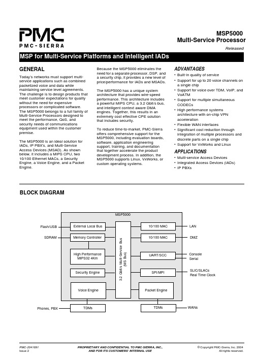
MSP5000ReleasedMSP for Multi-Service Platforms and Intelligent IADsMulti-Service ProcessorPMC-2041691 PROPRIETARY AND CONFIDENTIAL TO PMC -SIERRA, INC.,© Copyright PMC-Sierra, Inc. 2004Issue 2AND FOR ITS CUSTOMERS’ INTERNAL USE All rights reserved.GENERALToday’s networks must support multi-service applications such as combined packetized voice and data whilemaintaining service level agreements. The challenge is to design products that meet customer expectations for quality without the need for expensiveprocessors or complicated software.The MSP5000 belongs to a full family of Multi-Service Processors designed to meet the performance, QoS, and security needs of communications equipment used within the customer premise.The MSP5000 is an ideal solution for IADs, IP PBX's, and Multi-Service Access Devices (MSAD). As shown below, it includes a MIPS CPU, two 10/100 Ethernet MACs, a Security Engine, a Voice Engine, and a Packet Engine.Because the MSP5000 eliminates the need for a separate processor, DSP, and a security chip, it provides a new level of price/performance for IADs and MSADs.The MSP5000 has a unique system architecture that provides wire-speed performance. This architecture includes a powerful MIPS CPU, a 3.2 Gbit/s bus, and intelligent context aware DMA engines. Together, this results in an extremely cost effective CPE solution that includes security.To reduce time-to-market, PMC-Sierra offers comprehensive support for the MSP5000, including evaluation boards, software, application engineering support, training, and documentation that together accelerate the product development process. In addition, the MSP5000 supports Linux, VxWorks, or custom operating systems.ADVANTAGES•Built-in quality of service•Support for up to 20 voice channels on a single chip•Support for voice over TDM, VoIP, and VoATM•Support for multiple simultaneous CODECs•High performance systems architecture with on-chip VPN acceleration•Flexible WAN interfaces•Significant cost reduction through integration of multiple processors and discrete parts on a single chip •Support for VxWorks and LinuxAPPLICATIONS•Multi-service Access Devices•Integrated Access Devices (IADs)•IP PBXsBLOCK DIAGRAM3.2 G b i t /s M u l t i -S e r v i c e B u s (M S B u s )External Local Bus Memory ControllerHigh Performance MIPS32 4KmMSP5000LAN Console DMZSDRAMFlash/USB Security Engine SPI/MPIUART/SCC10/100 MAC10/100 MAC Voice Engine TDMs WANsPacket EngineSerialSLIC/SLACs Real Time ClockTDMs Phones, PBXHead Office:PMC-Sierra, Inc.8555 Baxter PlaceBurnaby, B.C. V5A 4V7CanadaTel: 1.604.415.6000Fax: 1.604.415.6200MSP for Multi-Service Platforms and Intelligent IADsTo order documentation, send email to:document@ or contact the head office,Attn: Document CoordinatorPMC-2041691 (R2)© Copyright PMC-Sierra, Inc. 2004. All rights reserved.For a complete list of PMC-Sierra’s trademarks and registered trademarks, visit: /legal/PROPRIETARY AND CONFIDENTIAL TO PMC-SIERRA, INC., AND FOR ITS CUSTOMERS’ INTERNAL USEMSP5000 Multi-Service ProcessorAll product documentation is available on our web site at: For corporate information,send email to:info@ELECTRICAL•369 pin PBGA•Vcc 3.3V I/O, 1.8V core •Power consumption 2WSYSTEM PROCESSOR•High performance MIPS32 4Km processor at 150 MHz•16 KB instruction cache, 16 KB data cacheULTRAFAST MULTI-SERVICE BUS (MS BUS)•Peak bandwidth of 3.2 Gbit/s •True parallel processing•Fast path – low latency voice processing•Prioritized accessVOICE ENGINE•LSI ZSP processor up to 125 MHz •80 KB instruction, 80 KB data on-chip SRAM•ADPCM hardware acceleratorTELEPHONY INTERFACE•Dual TDM interfaces each capable of 128 full duplex channelsPACKET ENGINE•LSI ZSP processor up to 125 MHz •80 KB instruction, 80 KB data on-chip SRAMWAN INTERFACE OPTIONS•UTOPIA I/II interface•Two Synchronous serial interfaces •LAN Interface•Two Independent 10/100 Ethernet MACs (MII or 7-wire)•Supports VLAN tagging and DMZSECURITY ENGINE•Hardware accelerator for DES, 3DES, MD5, and SHA-1•IPSec compliantSYSTEM CONTROL•Eight interrupt inputs •GPIOs•MIPS timer, two system timers, and watchdog timer •Block copy engine•Flexible external local bus interfaceMISCELLANEOUS INTERFACES•UART •SPI/MPI•Two-wire serial•Two Serial communications controllers (asynchronous, synchronous, HDLC)MEMORY CONTROLLER•Glueless interface to 128 MB of SDRAM•Glueless interface to 32 MB of flashPACKET ENGINE FIRMWARE•AAL0, AAL1, AAL2, AAL5, ATM SAR, OAM-F5 (loop back)•RFC1483 - Multiprotocol ncapsulation over AAL5•QoS•CES supportVOICE PROCESSING•Voice CODECs (G.711, G.726, G.729a/b, G.723.1)•G.168 echo cancellers•G.711-Fax, fax/modem tone detection •T.38 Fax relay•DTMF generation/detection •Call progress generation •Caller ID•Voice activity detection and comfort noise•Silence suppression•Channel cross-switch and conferencing •Gain control •Jitter buffer•Adaptive clocking •Packet playout•Hardware Fastpath (VoATM)•BLES VoATM profiles (9,10,11)•VoIP Inband caller ID/DTMF processing of fax•CODEC switching and simultaneous multiple CODECsSOFTWARE•APIs: Voice and Packet engines, MACs, Security engine, and Block Copy•Sample code for voice gatewayinteroperability verification, signaling, and switching•Sample drivers for selected WAN options (G.SHDSL, SDSL, T1)CERTIFICATIONS•NIST certification for securityalgorithms (FIPS 46-3, 81, and 180-1)DEVELOPMENT TOOLS•Support for Linux and VxWorks •Evaluation boardsTHIRD PARTY SUPPORT•Security Applications•Ashley Laurent - Broadway Engine •INTOTO - iGateway•SofaWare Technologies - Safe@Office •Voice Processing•GIPS - Global IP Sound - NetEq •RADVISION - H.323, SIP, MGCP •EJTAG Debuggers •EPI - MAJIC probe•WindRiver - visionICE II。
MSP430F2XX中文手册(加了标签) 5.Flash块控制器

Page 1 of 18MSP430F2系列16位超低功耗单片机模块原理第5章 Flash 块控制器版本: 1.3日期: 2007.6.原文: TI MSP430x2xxfamily.pdf翻译: 余川编辑: DC 微控技术论坛版主注:以下文章是翻译TI MSP430x2xxfamily.pdf 文件中的部分内容。
由于我们翻译水平有限,有整理过程中难免有所不足或错误;所以以下内容只供参考.一切以原文为准。
详情请密切留意微控技术论坛。
第五章 Flash 存储控制器本章介绍了MSP430x2xx 系列单片机Flash 存储控制器的操作。
5.1 Flash 存储器的介绍Page 2 of 18 5.2 Flash 存储器的分段结构5.3 Flash 存储器的操作5.4 Flash 存储器的控制寄存器5.1 Flash 存储器的介绍MSP430 的F lash 存储器是可位/字节/字寻址和编程的存储器。
该模块由一个集成控制器来控制编程和擦除的操作。
控制器包括三个寄存器,一个时序发生器及一个提供编程/擦除电压的电压发生器。
MSP430 的F lash 存储器的特点有:● 产生内部编程电压● 可位/字节/字编程● 超低功耗操作● 支持段擦除和多段模块擦除F lash 存储器和控制器的结构框图如图5−1所示。
注意:F lash 写入和擦除操作期间的最小电压值V CC 应为2.2V 。
如果在操作期间V CC 低于2.2V ,写入或擦除的结果将是不确定的。
图5−1 F lash 存储器框图Page 3 of 185.2 Flash 存储器的分段结构MSP430 F lash 存储器分成多个段。
可对其进行单个位/字节/字的写入,但是最小的擦除单位是段。
F lash 存储器分为主存储器和信息存储器两部分,在操作上两者没有什么区别,程序代码和数据可以存储于任意部分。
两部分的区别在于段的大小和物理地址。
信息存储器有四个64字节的段,主存储器有两个或更多的512字节的段。
MSP432P401R 用户指南
MSP432P401R 用户指南1. 引言本文档旨在为使用MSP432P401R微控制器的开发者提供详细的用户指南。
MSP432P401R是德州仪器(TI)推出的一款低功耗、高性能的ARM Cortex-M4F 内核微控制器。
本指南将帮助用户了解MSP432P401R的基本特性、功能模块和使用方法。
2. 概述MSP432P401R微控制器是基于ARM Cortex-M4F内核的32位单片机。
与其他MSP微控制器相比,MSP432P401R具有更低的功耗和更高的性能。
它采用了TI 的低功耗技术,使得在高性能运算的同时,整个系统的功耗仅为几个微瓦。
MSP432P401R具有丰富的外设功能,包括数字IO、模拟IO、时钟和定时器。
它还支持各种通信接口,如UART、SPI和I2C,以及模拟模块,如ADC和DAC。
此外,MSP432P401R还集成了多个片上内存和闪存,以及一些特殊模块,如低功耗计时器(RTC)和DMA控制器。
3. 特性3.1 处理器MSP432P401R采用ARM Cortex-M4F内核,运行频率高达48MHz。
它具有高性能的浮点单元(FPU),可加速浮点运算,支持单精度和双精度浮点数操作。
此外,MSP432P401R还集成了硬件除法器,可执行快速的整数除法操作。
3.2 存储器MSP432P401R具有256KB的闪存和64KB的RAM。
闪存用于存储用户程序和数据,RAM用于存储运行时数据。
此外,MSP432P401R还具有额外的片上存储器,如EEPROM和FRAM,可供用户进行非易失性数据存储。
3.3 时钟和定时器MSP432P401R支持多个时钟源,包括外部晶体振荡器、内部RC振荡器和低功耗振荡器。
它还具有多个定时器模块,包括通用定时器和低功耗定时器,可用于生成精确的时间延迟和定时事件。
3.4 通信接口MSP432P401R支持多种通信接口,包括UART、SPI和I2C。
通过这些接口,可以实现与其他外部设备的数据交换和通信。
MSP430PDF中文版PDF资料

指令集描述P(220—257)* DECX.A目的操作数减1* DECX.[W] 目的操作数减1* DECX.B 目的操作数减1语法DECV.A dstDECX dst 或DECX.W dstDECX.B dst操作dst – 1 →dst仿真SUBX.A#1,dstSUBX #1,dstSUBX.B #1,dst说明目的操作数减1 以前的内容丢失状态位N :结果为负时置位为正时复位Z : dst包含1时置位其他情况时复位C : dst包含0时置位其他情况时复位V : 产生算术溢出时置位其他情况时复位目的操作数的初始值为08000H时置位其他情况时复位方式位OscOff(晶振控制位),CPUOff(CPU控制位)和GIE(中断标志位)不受影响例子目的地址操作数减一DECX.A TONI ; TONI减一* DECDX.[W] 目的操作数减2* DECDX.B 目的操作数减2语法DECDX.A dstDECDX dst or DECDX.W dsDECDX.B dst操作dst - 2 -> dst仿真SUBX.A#2,dstSUBX #2,dstSUBX.B #2,dst说明目的操作数减2 以前的内容丢失状态位N : 结果为负时置位为正时复位Z : dst包含2时置位其他情况时复位C : dst包含0或1时置位其他情况时复位V : dst产生算术溢出时置位其他情况时复位目的操作数的初始值为08001H或08000H时置方式位OscOff, CPUOff 和GIE不受影响例子目的地址操作数减二DECDX.A TONI ; Decrement TONI* INCX.[W] 目的操作数加1* INCX.B 目的操作数加1语法INCX.A dstINCX dst or INCX.W dstINCX.B dst操作dst + 1 →dst仿真ADDX.A#1,dstADDX #1,dstADDX.B #1,dst说明目的操作数加1 以前的内容丢失状态位N : 结果为负时置位为正时复位Z : dst包含0FFFFFH时置位其他情况时复位dst包含0FFFFH时置位其他情况时复位dst包含0FFFH时置位其他情况时复位C: dst包含0FFFFFH时置位其他情况时复位dst包含0FFFFH时置位其他情况时复位dst包含0FFFH时置位其他情况时复位V : dst包含07FFFH时置位其他情况时复位dst包含07FFFH时置位其他情况时复位dst包含07FH时置位其他情况时复位方式位OscOff ,CPUOff 和GIE不受影响例子目的地址操作数加一INCX.A TONI ; Increment TONI (20-bits)* INCDX.A目的操作数加2* INCDX.[W] 目的操作数加2* INCDX.B 目的操作数加2语法INCDX.A dstINCDX dst or INCDX.W dstINCDX.B dst操作dst + 1 →dst仿真ADDX.A#2,dstADDX #2,dstADDX.B #2,dst说明目的操作数加2以前的内容丢失状态位N: 结果为负时置位为正时复位Z : dst包含0FFFFEH时置位其他情况时复位dst包含0FFFEH时置位其他情况时复位dst包含0FEH时置位其他情况时复位C: dst包含0FFFFEH或0FFFFFH时置位其他情况时复位dst包含0FFFEH或0FFFFH时置位其他情况时复位dst包含0FEH或0FFH时置位其他情况时复位V: dst包含07FFFEH或0FFFFH时置位其他情况时复位dst包含07FFEH或0FFFH时置位其他情况时复位dst包含07EH或0FH时置位其他情况时复位方式位OscOff ,CPUOff 和GIE不受影响例子目的地址操作数加二INCDX.B LEO ; Increment LEO by two* INVX.A目的操作数求反* INVX.[W] 目的操作数求反* INVX.B 目的操作数求反语法INVX.A dstINVX dst or INVX.W dstINVX.B dst操作.NOT.dst →dst仿真XORX.A#0FFFFFh,dstXORX #0FFFFh,dstXORX.B #0FFh,dst说明目的操作数取反以前的内容丢失状态位N : 结果为负时置位为正时复位Z :dst 包含0FFFFFH时置位其他情况时复位dst 包含0FFFFH时置位其他情况时复位dst 包含0FFH时置位其他情况时复位C :结果不为零时置位其他情况时复位( = .NOT.Zero )V 初始目的操作数为负时置位其他情况时复位方式位OscOff CPUOff 和GIE不受影响例子R5 求反INVX.A R5 ; R5求反MOVX.A源操作数移至目的操作数MOVX.[W] 源操作数移至目的操作数MOVX.B 源操作数移至目的操作数语法MOVX.A src,dstMOVX src,dst or MOVX.W src,dstMOVX.B src,dst操作src →dst说明源操作数被移至目的操作数源操作数不受影响目的操作数以前的内容丢失状态位N: 不影响状态位Z: 不影响状态位C: 不影响状态位V: 不影响状态位方式位OscOff ,CPUOff 和GIE不受影响例子移动18000H 到EDEMOVX. A#018000h, &EDE ; Move 18000h to EDE例子地起码表EDE(字数据)的内容被复制到表TOM 地址表的长度为030H MOV #EDE, R10 ;准备指针Loop MOV @R10+, TOM-EDE-2(R10) ;将R10 中的指针用于两表DEC R9 ;计数器减1JNZ Loop ;计数器<>0 继续........ ;完成例子地起码表EDE(字数据)的内容被复制到表TOM 地址表的长度为020H MOV #EDE, R10 ;准备指针MOV #020H, R9 ;计数器Loop MOV @R10+, TOM-EDE-2(R10) ;将R10 中的指针用于两表DEC R9 ;计数器减1JNZ Loop ;计数器<>0 继续........ ;完成28种MOVX寻址方式中的10种,一个指令可以使用MOVX,这样可以节省二个字节编码周期。
[计算机软件及应用]15MSP430中文用户指南
![[计算机软件及应用]15MSP430中文用户指南](https://img.taocdn.com/s3/m/b69a5036443610661ed9ad51f01dc281e53a5681.png)
T EXAS I NSTRUMENTSMSP430系列混合信号微控制器结构及模块用户指南目录1MSP430系列1.1特性与功能1.2系统关键性能1.3MSP430系列的各型号2结构概述2.1CPU2.2代码存储器2.3数据存储器(RAM)2.4运行控制2.5外围模块2.6振荡器、倍频器和时钟发生器3系统复位、中断和运行模式3.1系统复位和初始化3.2中断系统结构3.3中断处理3.3.1SFR中的中断控制位3.3.2外部中断3.4运行模式3.5低功耗模式3.5.1 低功耗模式0与模式1,LPM0和LPM1 3.5.2 低功耗模式2与模式3,LPM2和LPM3 3.5.3 低功耗模式4,LPM43.6 低功耗应用要点4 存储器组织4.1 存储器中的数据4.2 片内ROM组织4.2.1 ROM表的处理4.2.2 计算分支跳转和子程序调用4.3 RAM与外围模块组织4.3.1 RAM4.3.2 外围模块—地址定位4.3.3 外围模块--SFR5 16位CPU5.1 CPU寄存器5.1.1 程序计数器PC5.1.2 系统堆栈指针SP5.1.3 状态寄存器SR5.1.4 常数发生寄存器CG1与CG25.2 寻址模式5.2.1 寄存器模式5.2.2 变址模式5.2.3 符号模式5.2.4 绝对模式5.2.5 间接模式5.2.6 间接增量模式5.2.7 立即模式5.2.8 指令的时钟周期与长度5.3 指令组概述5.3.1 双操作数指令5.3.2 单操作数指令5.3.3 条件跳转5.3.4 模拟指令的短格式5.3.5 其它指令5.4 指令分布6 硬件乘法器6.1 硬件乘法器的操作6.2 硬件乘法器的寄存器6.3 硬件乘法器的SFR位6.4 硬件乘法器的软件限制6.4.1 硬件乘法器软件限制--寻址模式 6.4.2 硬件乘法器软件限制--中断程序7 振荡器与系统时钟发生器7.1 晶体振荡器7.2 处理机时钟发生器7.3 系统时钟运行模式7.4 系统时钟控制寄存器7.4.1 模块寄存器7.4.2 与系统时钟发生器相关的SFR位 7.5 DCO典型特性8 数字I/O配置8.1 通用端口P08.1.1 P0控制寄存器8.1.2 P0原理图8.1.3 P0中断控制功能8.2 通用端口P1、P28.2.1 P1、P2控制寄存器8.2.2 P1、P2原理图8.2.3 P1、P2中断控制功能8.3 通用端口P3、P48.3.1 P3、P4控制寄存器8.3.2 P3、P4原理图8.4 LCD端口8.5 LCD端口--定时器/端口比较器9 通用定时器/端口模块9.1 定时器/端口模块操作9.1.1 定时器/端口计数器TPCNT1,8位操作 9.1.2 定时器/端口计数器TPCNT2,8位操作 9.1.3 定时器/端口计数器,16位操作9.2 定时器/端口寄存器9.3 定时器/端口SFR位9.4 定时器/端口在A/D中的应用9.4.1 R/D转换原理9.4.2 分辨率高于8位的转换10 定时器10.1 Basic Timer110.1.1 BasicTimer1寄存器10.1.2 SFR位10.1.3 BasicTimer1操作10.1.4 BasicTimer1操作:LCD时钟信号f LCD 10.2 8位间隔(Interval)定时器/计数器 10.2.1 8位定时器/计数器的操作10.2.2 8位定时器/计数器的寄存器10.2.3 与8位定时器/计数器有关的SFR 10.2.4 8位定时器/计数器在UART中的应用 10.3 看门狗定时器10.3.1 看门狗定时器寄存器10.3.2 看门狗定时器中断控制功能10.3.3 看门狗定时器操作10.4 8位PWM定时器10.4.1 操作10.4.2 PWM寄存器11 Timer_A11.1 Timer_A的操作11.1.1 定时器操作11.1.2 捕获模式11.1.3 比较器模式11.1.4 输出单元11.2 Timer_A的寄存器11.2.1 Timer_A控制寄存器TACTL11.2.2 捕获/比较控制寄存器CCTL11.2.3 Timer_A中断向量寄存器11.3 Timer_A的应用11.3.1 Timer_A增计数模式应用11.3.2 Timer_A连续模式应用11.3.3 Timer_A增/减计数模式应用11.3.4 Timer_A软件捕获应用11.3.5 Timer_A处理异步串行通信协议 11.4 Timer_A的特殊情况11.4.1 CCR0用作周期寄存器11.4.2 定时器寄存器的启/停11.4.3 输出单元Unit012 USART外围接口,UART模式12.1 异步操作12.1.1 异步帧格式12.1.2 异步通信的波特率发生器12.1.3 异步通信格式12.1.4 线路空闲多处理机模式12.1.5 地址位格式12.2 中断与控制功能12.2.1 USART接收允许12.2.2 USART发送允许12.2.3 USART接收中断操作12.2.4 USART发送中断操作12.3 控制与状态寄存器12.3.1 USART控制寄存器UCTL12.3.2 发送控制寄存器UTCTL12.3.3 接收控制寄存器URCTL12.3.4 波特率选择和调制控制寄存器12.3.5 USART接收数据缓存URXBUF12.3.6 USART发送数据缓存UTXBUF12.4 UART模式,低功耗模式应用特性 12.4.1 由UART帧启动接收操作12.4.2 UART模式波特率与时钟频率12.4.3 节约MSP430资源的多处理机模式 12.5 波特率的计算13 USART外围接口,SPI模式13.1 USART的同步操作13.1.1 SPI模式中的主模式,MM=1、SYNC=1 13.1.2 SPI模式中的从模式,MM=0、SYNC=1 13.2 中断与控制功能13.2.1 USART接收允许13.2.2 USART发送允许13.2.3 USART接收中断操作13.2.4 USART发送中断操作13.3 控制与状态寄存器13.3.1 USART控制寄存器13.3.2 发送控制寄存器UTCTL13.3.3 接收控制寄存器URCTL13.3.4 波特率选择和调制控制寄存器 13.3.5 USART接收数据缓存URXBUF 13.3.6 USART发送数据缓存UTXBUF14 液晶显示驱动14.1 LCD驱动基本原理14.2 LCD控制器/驱动器14.2.1 LCD控制器/驱动器功能14.2.2 LCD控制及模式寄存器14.2.3 LCD显示存储器14.2.4 LCD操作软件例程14.3 LCD端口功能14.4 LCD与端口模式混合应用实例15 A/D转换器15.1 概述15.2 A/D转换操作15.2.1 A/D转换15.2.2 A/D中断15.2.3 A/D量程15.2.4 A/D电流源15.2.5 A/D输入端与多路切换15.2.6 A/D接地与降噪15.2.7 A/D输入与输出引脚15.3 A/D控制寄存器16 其它模块16.1 晶体振荡器16.2 上电电路16.3 晶振缓冲输出附录A 外围模块分布附录B 指令组说明附录C EPROM编程本书用途及表述约定MSP430用户指南以方便工程师及程序员使用的方式提供软件和硬件资料,以帮助开发应用MSP430系列的产品。
MSP430F13X_14X系列中文数据手册.

MSP430x13x , MSP430x14x , MSP430x14x1混合信号微控制器低电源电压范围:1.8~3.6V超低功耗:待机模式:1.6uA关闭模式 (RAM保持 :0.1uA活动模式:280uA at 1MHz, 2.2V5种省电模式6us 内从待机模式唤醒16位 RISC 结构, 125ns 指令周期带内部参考,采样保持和自动扫描特性的 12位 A/D转换器有 7个捕获 /比较寄存器的 16位定时器 Timer_B有 3个捕获 /比较寄存器的 16位定时器 Timer_A片内集成比较器串行在线编程,无需外部编程电压,安全熔丝可编程代码保护 .器件系列包括:–MSP430F133:8KB+256B闪速存储器, 256B 的 RAM–MSP430F135:16KB+256B闪速存储器, 512B 的 RAM–MSP430F147, MSP430F1471:32KB+256B闪速存储器, 1KB 的 RAM –MSP430F148, MSP430F1481:48KB+256B闪速存储器, 2KB 的 RAM–MSP430F149, MSP430F1491:60KB+256B闪速存储器, 2KB 的 RAM可用封装:64脚方形扁平封装 (QFP.描述德州仪器的 MSP430系列是一种超低功耗微控制器系列,由针对各种不同应用模块组合特性的多种型号组成.微控制器可设计成使用电池长时间工作.由于其 16位的体系结构, 16位的 CPU 集成寄存器和常数发生器, 可使 MSP430实现了最大化的代码效率。
数字控制振荡器使所有低功率模式唤醒到运行模式小于 6us 的唤醒时间。
MSP430x13x 和 MSP430x14x 系列是有两个内置 16位定时器,一个快速 12位 A/D转换器,一或两个通用串行同步 /异步通信接口 (USART和 48个 I/O引脚构造的微控制器。
典型应用为传感器系统,把模拟信号转换成数字值,处理并发送数据到主系统。
MSP430中文选型手册

MSP430超低功耗微处理器无所不在的 MCU总有一款 430 适合您2009年第三季度免费的代码限制版 Code Composer Essentials (16 kB ) 与 IAR (4/8/16 kB ) 软件。
支持器件价格1All$ 99All (8 devices at one time)$ 199All$ 49目标板与编程器目标板(无编程器)MSP-FET430U14 MSP-FET430U28 MSP-FET430U23x0 MSP-FET430U38 MSP-FET430U48MSP-FET430U64 MSP-TS430PM64MSP-FET430U64A MSP-TS430PM64A MSP-FET430U80 MSP-FET430U80USB MSP-TS430PN80USBeZ430-RF2500价格1 Complete development system with detachable target board and USB emulator. Ideal for new users. $20 Wireless development system including two detachable 2.4GHz wireless target boards and USB emulator. $49ZigBee development system including three detachable ZigBee target boards and USB emulator. $99 Solar Energy Harvesting development system. A battery-less wireless sensor network. $149$10 2.4GHz wireless target board for expanding your wireless network (emulator required). $20红色粗体标注的为新产品。
MSP430F5系列中文手册1.1版第4章 PMM电源管理与供电监控

MSP430F5系列16位超低功耗单片机模块原理第4章PMM 电源管理模块与供电监控版本: 1.1发布日期: 2008.7. 最后更新日期:2010.8.原文: TI slau208.pdf (5xxfamily User's Guide)翻译: 田萍果西安工业大学编辑: DC 微控网总版主注:以下文章是翻译TI slau208.pdf 文件中的部分内容。
由于我们翻译水平有限,有整理过程中难免有所不足或错误;所以以下内容只供参考.一切以原文为准。
文章更新详情请密切留意微控技术论坛。
第11章PMM 电源管理模块与供电监控4.1 电源管理简介电源管理特征:.提供宽的电源电压范围:1.8V-3.6V.产生的核心电压(V CORE):1.4V,1.6V,1.8V和1.9V(典型值).欠压复位(BOR).配有DVCC 和VCORE的电源电压管理.DVCC 和VCORE的电源电压监测有8个可编程级别.软件恢复掉电时系统状态.掉电条件下软件可选择上电复位.上电失败时有I/O保护.软件可选监视状态输出(可选)MSP430主要数字逻辑需要一个低于DVCC允许范围的电压。
因此,电源管理模块集成了一个低压降的电压调整器(LDO),LDO可以产生一个二次核心电压VCORE。
这个核心电压可通过四步编程从而使功耗最低化。
核的最小允许电压依赖于选择的MCLK大小,如4-1图所示。
我们可以管理和监控DV CC and V CORE。
当电压降到特殊阈值以下时管理和监控就工作了。
通常来讲,管理会致使上电复位事件发生(POR),而监控产生中断标志,这时软件就可以处理了。
比如说,DV CC(LDO 的高电平)分别被高电平管理(SVS H)和高电平监测器(SVM H)所管理和监测;V CORE(LDO的低电平)分别被低电平管理(SVS L)和低电平监测器(SVM L)所管理和监测. 电源管理单元框图如图4-2所示。
I/O口和所有模拟单元包括晶振在内都由DV CC供电。
MSP430F4XX中文技术手册

– MSP430F412: 4KB + 256B Flash Memory,256B RAM;
– MSP430F413: 8KB + 256B Flash Memory,256B RAM;
MSP430单片机数据手册—英
IMPORTANT NOTICETexas Instruments Incorporated and its subsidiaries (TI) reserve the right to make corrections, modifications, enhancements, improvements, and other changes to its products and services at any time and to discontinue any product or service without notice. Customers should obtain the latest relevant information before placing orders and should verify that such information is current and complete. All products are sold subject to TI’s terms and conditions of sale supplied at the time of order acknowledgment.TI warrants performance of its hardware products to the specifications applicable at the time of sale in accordance with TI’s standard warranty. T esting and other quality control techniques are used to the extent TI deems necessary to support this warranty. Except where mandated by government requirements, testing of all parameters of each product is not necessarily performed.TI assumes no liability for applications assistance or customer product design. Customers are responsible for their products and applications using TI components. T o minimize the risks associated with customer products and applications, customers should provide adequate design and operating safeguards.TI does not warrant or represent that any license, either express or implied, is granted under any TI patent right, copyright, mask work right, or other TI intellectual property right relating to any combination, machine, or process in which TI products or services are used. Information published by TI regarding third-party products or services does not constitute a license from TI to use such products or services or a warranty or endorsement thereof. Use of such information may require a license from a third party under the patents or other intellectual property of the third party, or a license from TI under the patents or other intellectual property of TI.Reproduction of information in TI data books or data sheets is permissible only if reproduction is without alteration and is accompanied by all associated warranties, conditions, limitations, and notices. Reproduction of this information with alteration is an unfair and deceptive business practice. TI is not responsible or liable for such altered documentation.Resale of TI products or services with statements different from or beyond the parameters stated by TI for that product or service voids all express and any implied warranties for the associated TI product or service and is an unfair and deceptive business practice. TI is not responsible or liable for any such statements. Following are URLs where you can obtain information on other Texas Instruments products and application solutions:Products ApplicationsAmplifiers Audio /audioData Converters Automotive /automotiveDSP Broadband /broadbandInterface Digital Control /digitalcontrolLogic Military /militaryPower Mgmt Optical Networking /opticalnetwork Microcontrollers Security /securityTelephony /telephonyVideo & Imaging /videoWireless /wirelessMailing Address:Texas InstrumentsPost Office Box 655303 Dallas, Texas 75265Copyright 2004, Texas Instruments Incorporated。
MSP430F2XX中文手册(加了标签) 1..MSP430体系结构

MSP430F2系列16位超低功耗单片机模块原理第1章MSP430体系结构版本: 1.3日期: 2007.4.原文: TI MSP430x2xxfamily.pdf翻译: 袁德纯编辑: DC 微控论坛版主注:以下文章是翻译TI MSP430x2xxfamily.pdf 文件中的部分内容。
由于我们翻译水平有限,有整理过程中难免有所不足或错误;所以以下内容只供参考.一切以原文为准。
详情请密切留意微控技术论坛。
Page 1 of 7第一章 MSP430的体系结构本章主要描述了MSP430的体系结构本章内容目录1.1MSP430的体系结构1.2可编程时钟系统1.3嵌入式仿真环境1.4地址空间1.5MSP430X2XX系列的提高1.1MSP430的体系结构将MSP430内部的16位精简指令集的CPU通过冯.诺依曼结构的地址总线和数据总线连接到外围设备和可编程时钟系统。
由于有一个先进的CPU配合具有标准组件存储印象的模拟和数字的外围设备,使得MSP430可用于处理混合信号。
MSP430x2xx系列的主要特性如下:◆超低功耗延长了电池的使用寿命●保持RAM 0.1uA●实时时钟模式 0.8uA●MIPS运行 250uA◆理想精确的模拟信号测量●门控比较定时器测量电阻类元件◆16位的精简指令集的CPU全新应用●更大的寄存器空间消除了运行空间的瓶颈●紧凑的核结构设计减少了功耗、降低了成本●使得高水平的编程更优化●27条核心指令和7种寻址方式●强大的矢量中断能力◆系统内的可编程FLASH使改变代码、在线升级和数据载入更灵活1.2 可编程时钟系统时钟系统是为电池供电系统而特别设计的。
只需要一个32KHZ的晶振就可以直接驱动一个低频的辅助时钟(ACLK)。
ACLK可工作于实时时钟模式,并具能够自我唤醒。
内部集成了一个DCO使主时钟(MCLK)可以被CPU和其他的高速外围设备所使用。
由于有了DCO,使得一个窄脉冲在少于2US 的时间内就可以将MSP430唤醒CPU工作。
MSP430 Ultra-Low-Power MCUs 数据手册说明书
MSP430 Ultra-Low-Power MCUsModular ArchitectureFlashClock SystemWatchdogRISC CPU 16-BitJ T A G /D e b u gACLKSMCLK MABMDBAnalog Peripheral DigitalPeripheralMCLKACLKSMCLKRAMPortMSP430 Modern Orthogonal 16-Bit RISC CPUThe MSP430 CPU core with sixteen 16-bitregisters, 27 single-cycle instructions and seven addressing modes results in higher processing efficiency and code density.MSP430 ArchitectureA 16-bit RISC CPU, peripherals and flexible clock system are combined by using a von-Neumann common memory address bus (MAB) and memory data bus (MDB). Partnering a modern CPU with modular memory-mapped analog and digital peripherals,the MSP430 offers solutions fortoday’s and tomorrow’s mixed-signal applications.Memory Options• Flash, ROM, OTP versions (from 1 kB to 60 kB)• RAM up to 10 kBAnalog Peripherals•High-performance ADC •Dual DACs •Comparator •LCD driver• Supply Voltage Supervisor (SVS)Digital Peripherals•USART/I2C•Hardware multiplier • 16-bit and 8-bit timers • DMA controllerModern 16-Bit RISC CPU• Large register file eliminates accumulator bottleneck •Optimized for C and assembler programming•Compact core design reduces power and cost•Up to 8 MIPS of performance available The MSP430’s orthogonal archi-tecture provides the flexibility of 16 fully addressable, single-cycle 16-bit CPU registers and the power of a RISC instruction set. The modern design of the CPU offers versatility through simplicity using only 27 easy-to-understandinstructions and seven consistent-addressing modes. This results in a 16-bit low-power CPU that has more effective processing, is smaller-sized, and more code-efficient than other 8/16-bit microcontrollers.Now it’s possible to develop new ultra-low-power, high-performance applications at a fraction of the code size.ADC12 with 200 ksps+, auto-scan, V REF , temperature sensor, and programmable sample and hold intervals.tStand-ByActiveActiveMultiple Oscillator Clock SystemUltra-Low-Power Activity ProfileADC12Flexible Clock System•Low-frequency auxiliary clock —Ultra-low-power stand-by mode •High-speed master clock—High-performance processing •Stability over time and temperature The MSP430 clock system is designed specifically for battery-powered applications. Multiple oscillators are utilized to support event-driven burst activity. A low frequency Auxiliary Clock (ACLK) is driven directly from a common 32-kHz watch crystal—with no additional external compo-nents. The ACLK can be used for a background real-time clock self wake-up function. An integrated high-speed Digitally Controlled Oscillator (DCO)can source the master clock (MCLK)used by the CPU and high-speed peripherals. By design, the DCO is active and stable in less than 6 µs.MSP430-based solutions efficiently use 16-bit RISC CPU high-perform-ance in very short burst intervals.This results in very high-performance and ultra-low power consumption.High-Performance Analog•12-bit or 10-bit fast SAR ADC •14-bit hi-res SAR ADC •16-bit slope ADC •12-bit DACSeveral high-performance data con-verter solutions are available in the MSP430 family. Innovative comparator-gated timers are available on alldevices for high-resolution slope type conversions. This is ideal for measur-ing resistive sensors such as thermis-tors when coupled with a capacitor.A fast 200-ksps+ 12-bit ADC with very high-integration is available on the MSP430F13x/14x/16x/43x/44x and is ideal for demanding applica-tions such as electricity meters and digital motor control. MSP430x32x derivatives offer a 14-bit ADC with a programmable current source.1Suggested 10,000 unit resale price in U.S. dollars. 2V CC2.5-5.5V 3Planned release Q2 2003. 4Planned release Q4 2003. All production parts support industrial temperature range.Product Selection:If you are not sure which MSP430 device best fits the performance, cost and power needs of your applica-tion, please refer to the selection guide on the previous page or visit the MSP430 home page at /msp430Price per unit in U.S. dollars.MSP-FET430 Flash Emulation Tool•JTAG based real-time in-system emulation•Target board, interface box, cable and samples•CD-Rom includes Kickstart IDE, assembler, linker, simulator and 4-kB C-compilerThe Flash Emulation Tool (FET) supports complete in-system development and is available for all MSP430F1xx and MSP430F4xx Flash devices.Programming, assembler/C-source level debug, single stepping, multiple hardware breakpoints, full-speed operation and peripheral access are all fully supported in-system using JTAG. The FET comes complete with everything required to complete an entire project.Embedded Emulation with theMSP430•Development is in-system andsubject to the exact same char-acteristics of the final application•Non-obtrusive in portable andhigh-pin count situations•Common user software andphysical interfaceToday’s applications operating atlower voltages, with tighter pack-aging and higher-precision analog,benefit greatly from the MSP430’sin-system emulation approach. TheMSP430’s dedicated embeddedemulation logic resides on theactual device itself and is accessedvia industry standard JTAG usingno additional system resources.From the first day of development,firmware engineers can now unob-trusively develop and debug theirembedded code with full-speedexecution, breakpoints, and singlesteps in an application.Embedded emulation becomeseven more important with high-performance mixed-signal systemsthat must maintain the integrity ofmicrovolt analog signals. Signalintegrity is virtually impossible withcumbersome in-circuit emulatorsthat are sensitive to cablingcrosstalk. And unlike abstract back-ground debuggers, no time-sharingof system serial communicationresources is required with embed-ded emulation on the MSP430.By combining the flexibility ofin-system programmable Flashmemory, unobtrusive embeddedemulation, and a common userinterface, development time isreduced. And, should the situationarise, last minute code updates aswell as remote scheduled andunscheduled upgrades can alsobe made.180****0107800 79 11 37+34 902 35 40 28************* ***********。
Ikalogic SP209系列9通道200MSPS逻辑分析器数据手册说明书

SP209 Series9-Channels, 200MSPS logic analyzerProduct status: Active.22.NOV.2018─PRODUCT DATA SHEET(PRELIMINARY DATA)IKALOGIC S.A.S.19 Rue Columbia 87000 Limoges FRANCEIkalogic | SP209 series data sheet | 1Table of contentsTable of contents1 SP209 Series overview2 Typical applications2 Product highlights2 Main characteristics3 SP209(i) Interfaces3 Principle of operation4 Embedded memory vs streaming4 Versatile trigger system4 External trigger OUT specifications5 External trigger IN specifications5 Industrial port (SP209i only)5 What’s in the box6 Unpacking and first usage6 Status LEDs behavior6 Software quick start guide6 Capturing your first signal7 Mechanical data7 Model SP209i7 Model SP2097 Probes7 Software technical requirements8 Ordering information8 Certifications and regulations8 Document Revisions9Ikalogic | SP209 series data sheet | 2SP209 Series overviewSP209series logic analyzers and protocoldecoders offer in depth analysis of logic signalsand protocols with200MHz(5ns)timingresolution.9-channel operation allows8-bitparallel data to be captured along with a clock orstrobe signal.SP Series is composed of two devices,SP209and SP209i.Both offer9logic inputs,butSP209i integrates industrial receivers forCAN, LIN, RS232 and RS485 buses. 1Typical applicationsSP series logic analyzers are perfectlyadapted for demanding applications,where it is needed to capture logic signalswith maximum time resolution on all9channels.●Embedded systems debugging●Research and education●Serial protocols analysis, like I2C,SPI, UART or 1-Wire (non exhaustive list)●Industrial bus analysis: RS232,RS485, CAN, LIN●ADC diagnosticProduct highlights●Schmitt trigger input stages with adjustable thresholds●200 MHz sampling rate, with all 9 channels used.●External clock option (state mode), up to 50MHz●Precise trigger-In and trigger-Out signals on SMA ports1 I ndustrial receivers in the SP209i are multiplexed with one or more of the existing 9 logic channelsIkalogic | SP209 series data sheet | 3Main characteristicsTiming and measurements Sampling rate (MAX.) 200 MSPS External clock Max. rate (State mode) 50 MHz Logic Inputs digital bandwidth50 MHz Embedded memory 2 Gb2Trigger output Yes, via SMA connector External trigger inputYes, via SMA connectorLogic inputsNumber of channels 9Input impedance 200 KΩ || 8 pFThreshold circuits 3Adjustable logic level (for each threshold) 1.8, 2.5, 3.3, 5VAbsolute max voltage on digital inputsContinuous± 25 VPower requirements Input power connector Micro USB femaleInput current 500 mA Input voltage5 V ± 0.25 V Communication interfaceUSB 2.0 High Speed2DDR-3sampling memory is used to buffer samples before streaming to host computer.SP209(i) Interfaces1.Status LED2.9-CH logic probes input3.Trigger OUT SMA connector4.Trigger IN SMA connectorB (micro-B) port.6.Industrial port3Principle of operationSP209Series logic analyzers connects to a computer via a USBcable.A free software -called ScanaStudio -is used to configure the device and display captured signals. The software can also be used to further analyze the captured samples by decoding protocols like I2C, SPI or UART.Embedded memory vs streamingUSB based logic analyzers (ones that don’t have a display and rely on a computer for that matter)usually operate according to one of two schemes:●Using an e mbedded memory to store captured samples.Samples3Only on SP209i (industrial) version.Ikalogic | SP209 series data sheet | 4are later downloaded at a slowerspeed via the USB interface.Thishas the advantage of not beinglimited by USB transfer rate,buthas the disadvantage of limitedembedded memory.●Streaming captured samples overthe USB connection,at themaximum possible speed.Whilethis offers the advantage of avirtually unlimited memory(onlylimited by host computer’smemory),it has the disadvantageof limiting the sampling rate toUSB’s throughput.SP209combines the advantages of bothstreaming and embedded memorytechniques.An embedded2Gb DDR-3memory stores captured samples at200MHz sampling rate on all channels,while a USB interface compresses and transfers the data simultaneously,effectively emptying the embedded memory and making more room for new samples.This results is a logic analyzer that can capture dozens of minutes of logic signals activity on 9 channels at 200 MSPS.Versatile trigger systemSP209series offer a state of the art trigger system.It’s composed of two FlexiTrig®trigger engines,each FlexiTrig engine can be used in one of those modes:●Edge trigger●Pulse trigger (with minimum andmaximum pulse width)●Timed logic sequence●Protocol based trigger (e.g. I2C busaddress or serial UART character)●External trigger source Furthermore,the two trigger engines(called A and B hereafter)can becascaded in one of the following modes:● A then B (Wait until A triggers thenarm B trigger engine)● B then A● A and B (Trigger engines A and Bmust trigger, but in any order)● A or B (whoever triggers first) Finally,an external trigger output is always active,in all modes and generates a trigger pulse whenever a trigger condition is met and a capture starts.Signal specifications for External trigger input and output are detailed in following section.External trigger OUT specificationsThere is an internal data path delay of 20ns before external signals reach internal trigger engine(T0).When trigger event occurs,a10ms(T2)pulse is generated on the Trig Out port.This porthas a50Ωseries impedance allowing easy interfacing to50Ωinput devices.This can be used to synchronise the capture with other equipment like an oscilloscope.Polarity of the trigger can be set in software.There is also a10ns delay(T1) between internal trigger detection and Trig Out assertion.Therefore,the totaltime for an external event to generate a Trigger OUT pulse is T0+T1 = 30ns.Ikalogic | SP209 series data sheet | 5External trigger IN specificationsThe Trig In port allows to start acquisitionon an external event generated by another instrument.The minimum pulse width (T1)is 5ns.Polarity can be set in software.The input impedance is also software selectable (100kΩor 50Ω).The threshold level is 1.0V.T2,the time between external trigger in active edge and internal trigger engine assertion is 20ns.Industrial port (SP209i only)SP209i offer the possibility to connect directly to industrial buses,as opposed to logic channels which can only be connected to single ended logic level such as LVCMOS or LVTTL.Each one of the industrial inputs integrates a dedicated receiver circuit,perfectly adapted to each standard.For more reliability in an industrial context,each bus receiver is exposed via screw terminals.Adequate wires (6-30 AWG)should be used to connect SP209i to the the bus being probed .4Industrial receivers offer the advantage of visualizing exactly what a standard4Wires to connect SP209i to industrial bus are not provided.off-the-shelf transceiver would receive if connected to that bus.The list of the industrial inputs is detailed below:● 1 CAN bus receiver●2RS485bus receiver (can be combined to form a full duplex RS422 bus receiver) ● 2 RS232 receivers ●1 LIN bus receiverPlease refer to the SP209i casing for exact pinout.RS485 receiver specifications Max. baudrate50 Mbps Common Mode Operating range-7 V to +12 V Common Mode Input Impedance48 kΩ || 10 pF (preliminary)Common Mode voltage abs. max±15 V Differential Threshold voltage-125 mV Differential Fixed hysteresis 25 mVDifferential Input Impedance400 kΩ or 120 Ω Software selectable(preliminary)RS232 receiver specifications Max. baudrate 1.5 Mbps Operating range ±15 V Input Impedance 5 kΩ|| 50 pF (preliminary)Absolute max voltage ±20 V Threshold voltage 1.5 V Hysteresis300 mVIkalogic | SP209 series data sheet | 6CAN receiver specificationsMax. baudrate 8 MbpsCommon Mode Operatingrange±12 VCommon Mode InputImpedanceT.B.D.Common Mode Absolutemax voltage±24 VDifferential ModeOperating range-4 V to +9 VDifferential Thresholdvoltage700 mVDifferential Fixedhysteresis30 mV to 200 mVDifferential Input Impedance 25 kΩ||20 pF or 120 Ω Software selectable(preliminary)LIN receiver specificationsMax. baudrate 20 kbps Operating range (BAT pin) 6 V to 18 V Operating range (RX pin) 0 V to 18 VRX pull up resistance (toBAT)40 kΩ Abolute max voltage (BAT) ±24 V Abolute max voltage (RX) ±24 V Threshold voltage 0.5 * VBAT Hysteresis 0.12 * VBATPlease note that SP209i can still only capture9channels simultaneously.Industrial inputs are internallymultiplexed with logic inputs.It is recommended to connect the ground of the industrial bus being measured to the nearest ground screw terminal. What’s in the boxSP209series is shipped with the followingaccessories:●SP209(i) device●10 leads micro-grabber probes set(premium quality, custom Ikalogicdesign)● 1 meter length Micro-USB cable●Cable comb Unpacking and first usageWe recommend the user to start byidentifying all different components thatare provided,then connect the SP209device to a free USB port of yourcomputer using the provided USB cable.The LED should glow according to the table in the“Status LEDs behavior”section.Status LEDs behaviorStatus led can be in one of 3 states:Status LEDOrange Device powered up but notconnected to softwareWhite Fix Device powered up and connectedto softwareWhite blinking Device powered up, connected tosoftware and detecting activity onone of the logic channels.Software quick start guideStart by downloading latest version of ScanaStudio software w and following instructions to install bothIkalogic | SP209 series data sheet | 7 software and provided drivers.It isrecommended to restart your computerafter the software and drivers have beeninstalled.Once the software is installed,run it,and create a new workspace by selecting “SP209” or “SP209i” as the device type. Note:if at the point the device is not recognised by your computer,theScanaStudio workspace is created as ademo workspace or the status LEDs stays orange even after creating a ScanaStudio workspace, please follow those steps:●Ensure the USB port used candeliver at least 500mA.●Try switching to another machineif one is available.●If all the above fails,please contactIkalogic support. Capturing your first signalTo capture your first logic signals,please follow those steps:1.Connect the device via USBunch ScanaStudio and create anSP209(i) workspace.3.Connect the probes to SP209(i)and to your signals source4.Ensure the ground probe isconnected5.Check if the status LED is blinking:if it’s the case,it means the somelogic changes are already beingdetected on the probes.6.Hit the start button in ScanaStudioand wait until signals are captured. You can adjust the quantity of samples to capture by adjusting the number of samples in the device configuration tab. Mechanical dataAll SP209series devices casing are manufactured from anodized aluminum,able to withstand heavy duty usage in various harsh environments.All markings are laser engraved,ensuring important pinout information is not lost over time.Model SP209iWeight: 105 gm(All dimensions in mm)Model SP209Weight: 90 gm (preliminary)(All dimensions in mm)Ikalogic | SP209 series data sheet | 8ProbesProbes cables are made of 24AWG extra flexible silicone wires. All wires are black colored, but every wire has a whitemarking tube with the channel number (e.g. “1” or “GND”) and a colored sticker on the probe tip.(All dimensions in mm)Software technical requirementsDownload ScanaStudio software on so you can use your device on your favorite platform. SP209(i) and ScanaStudio were tested to supports the following platforms:●Windows 7/8/10●Mac OS 10.9 or later●Ubuntu 14.04 or laterOrdering informationFor ordering information, please check for nearest distributor on w or contact us for any inquiry at ********************.Certifications and regulationsThis device complies with the following applicable European Directives:Electromagnetic Compatibility (EMC) Directive 2004/108/EC,Low-Voltage Directive 2006/95/EC, IEC61326-2.This device complies with part 15of the FCC Rules. Operation is subject to the following two conditions:(1) This device may not cause harmful interference,and (2) this device must accept any interference received, including interference that may cause undesired operation.CAN ICES-3 (B) / NMB-3 (B)RoHS Compliant 2011/65/EC.This device does not contain any of the substances in excess of the maximum concentration values ("MCVs")defined in the EU RoHS Directive.NOTE:This equipment has been tested and found to comply with the limits for a Class B digital device, pursuant to part 15of the FCC Rules.These limits are designed to provide reasonable protection against harmful interference in a residential installation.This equipment generates uses and can radiate radio frequency energy and,if not installed and used in accordance with the instruction,may cause harmful interference to radio communications.However,there is no guarantee that interference will not occur in a particular installation.If this equipment does cause harmful interference to radio or television reception which can be determined by turning the equipment off and on,the user is encouraged to try to correct interference by one or more of the following measures: • Reorient or relocate the receiving antenna.•Increase the separation between the equipment and receiver.•Connect the equipment into an outlet on circuit different from that to which the receiver is connected. •Consult the dealer or an experienced radio/TV technician for help.Ikalogic | SP209 series data sheet | 9Document Revisions●22-November-2018:○Fixed error in “What’s in the box” chapter○Updated trigger OUT and trigger IN specifications○Updated device weight●10-October-2018: Initial release of this datasheet.This information is subject to change without notice. © Ikalogic SAS 2018, 。
- 1、下载文档前请自行甄别文档内容的完整性,平台不提供额外的编辑、内容补充、找答案等附加服务。
- 2、"仅部分预览"的文档,不可在线预览部分如存在完整性等问题,可反馈申请退款(可完整预览的文档不适用该条件!)。
- 3、如文档侵犯您的权益,请联系客服反馈,我们会尽快为您处理(人工客服工作时间:9:00-18:30)。
Jump-on-equal bit=0
表2 寻址方式说明
3.工作模式
MSP430有一个活动模式和五个软件可选的低功耗工作模式。一个中断事件可以把系统从各种低功耗模式唤醒,响应中断请求并且从中断程序中返回原来的低功耗模式。
以下六种工作模式可以通过软件进行配置:
1.活动模式(AM):所有时钟均被激活。
2.当满足最小的t cap时间和参数时,外部信号将触发捕获事件。即便捕获信号小于t cap 也可能触发捕获事件。为了确保获得16位定时器值和使标志位置位,周期和时间必须满足这些规范。
内部信号Tax,SMCLK at Timer_A
泄露电流(参阅注释1)
注释:1.除非另外说明,测量时对应引脚所加的电平为VSS或VCC
2.数字端口引脚的泄露电流要单个测量。端口引脚必须选择为输入并且没有选择上拉或下拉电阻。
输出 P2x,Tax
输出P1口和P2口
注释:1.对于所有输出组合,最大总电流I OH(max)和I OL(max)不能超过±12mA,以便输出电压满足输出电压下降标准。
2.对于所有输出组合,最大总电流I OH(max)和I OL(max)不能超过±36mA,以便输出电压满足输出电压下降标准。
产品说明
TI公司的MSP43O系列超低功耗微控制器由一些基本功能模块按照不同的应用目标组合而成。在便携式测量应用中,这种优化的体系结构结合五种低功耗模式可以达到延长电池寿命的目的。MSP430系列的CPU采用16位精简指令系统,集成有16位寄存器和常数发生器,发挥了最高的代码效率。它采用数字控制振荡器(DCO),使得从低功耗模式到唤醒模式的转换时间小于6μs.
MSP中文数据手册
MSP430混合信号微控制器数据手册
产品特性
●低电压范围:2.5V~5.5V
●超低功耗
——活动模式:330μA at 1MHz, 3V
——待机模式:0.8μA
——掉电模式(RAM数据保持):0.1μA
●从待机模式唤醒响应时间不超过6μs
●16位精简指令系统,指令周期200ns
●基本时钟模块配置
基本时钟模块提供了一下几种时钟信号:
1.辅助时钟(ACLK),由32768Hz外部晶体或者一个高频晶体产生
2.主时钟(MCLK),供CPU使用的系统时钟
3.子系统时钟(SMCLK),供外围模块使用的子系统时钟
数字I/O
共有两个8位的I/O接口---P1和P2(在外部引脚上只有6个P2I/O信号可用):
2.低功耗模式0(LPM0):CPU停止工作,外围模块继续工作,ACLK和SMCLK有效,MCLK的环路控制无效。
3.低功耗模式1(LPM1):CPU停止工作,外围模块继续工作,ACLK和SMCLK有效,MCLK的环路控制无效,如果数字控制振荡器(DCO)没有被用于活动模式,其DC发生器被关闭。
4. 低功耗模式2(LPM2):CPU停止工作,外围模块继续工作,ACLK有效,SMCLK和MCLK环路控制无效,DCO的DC发生器关闭。
OFIFG: 振荡器错误时置位.
NMIFG: 通过RST/NMI引脚置位
存储器组织
外围设备
外设通过数据、地址、控制总线与CPU相连,可以通过所有操作指令进行控制。完整的模块说明请参阅MSP43Ox11xx系列用户手册(文献号:SLAU049)。
振荡器和系统时钟
时钟系统由基本时钟模块支持,基本时钟模块包括一个内部数字控制振荡器、一个高频晶振和对一个32768Hz外部晶振的支持。基本时钟模块的这种设计既满足了低系统开销的要求,又满足了低功耗的要求。内部数字控制振荡器(DCO)提供了一个高速开启的时钟源,它尅在6μs内达到稳定。
●调节控制位MOD0到MOD4选择在32个DCO时钟周期的周期里f(DCO+1)被使用多少次,在剩余的时钟周期里使用频率f(DCO).这个频率是一个如下所示的平均值:
晶振,XIN,XOUT
注释:1.晶体两端都需要连接电容,电容值由晶体制造商规定。
2.仅当使用一个外部逻辑水平时钟源时适用,使用晶体或谐振器时不适用。
结束一个检查或者编程会话后,TEST引脚恢复低电平,熔丝检查模式和检测电流终止。
上电后,TMS引脚的第一个下降沿将激活熔丝检查模式,或者如果在上电期间TMS保持低电平,该模式也会激活。TMS引脚的第二个上升沿将关闭熔丝检查模式。该模式关闭后,熔丝检查模式保持无效直到另一个POR出现。在每一次POR,熔丝检查模式都有机会激活。
——多种内部电阻
——单个外部电阻
——32kHz晶振
——高频晶体
——谐振器
——外部时钟源
●带有三个捕获/比较寄存器的16位定时器(Timer_A)
●串行在线可编程
●采用保险熔丝的程序代码保护措施
●该系列产品包括
——MSP430C111:2K字节ROM,128字节RAM
——MSP430C112:4K字节ROM,256字节RAM
任意引脚上Leabharlann 电压(见注释)……………………………………-0.3V---VCC+0.3V
任意端点二极管电流……………………………………………………………±2mA
存储温度(未编程芯片)……………………………………………-55℃---150℃
存储温度(已编程芯片)……………………………………………-40℃----85℃
供电电流(进入VCC)不包括外部电流
注释:所有输入连接到VSS或VCC,输出悬空。
与系统频率相对应的活动模式下的电流消耗:
与供电电压相对应的活动模式下的电流消耗:
施密特触发式输入_P1和P2口
标准输入RST/NMI,TCK,TMS,TDI
输入Px.x,Tax
注释:1.外部信号每次将中断标志置位,t int 周期和时间参数必须满足条件。即使触发信号比t int短,也可能会使标志位置位。为了确保标志可靠置位,信号周期和时间都应满足条件。
1.中断使能寄存器1
WDTIE: 看门狗定时器中断使能位。当看门狗定时器被配置在间隔定时器模式时激活,当选中看门狗模式时不激活。
OFIE: 振荡器错误中断使能位。
NMIE: 非可屏蔽中断使能位。
2.中断标志寄存器1
WDTIFG:看门狗定时器溢出(看门狗模式下)或者保密密钥非法时置位,VCC上电或者复位模式下RST/NMI引脚引起复位时复位.
1.所有的单个I/O位均是独立可编程的
2.允许任意组合输入、输出和中断条件
3.P1口的所有8位和P2口的6位都可以用于处理外部中断处理
4.可以使用所有指令读写端口控制的寄存器
注释:外部引脚上只有P2口的6位,P2.0—P2.5,但为P2口分配了所有的控制位和数据位。
看门狗定时器
看门狗定时器(WDT)模块的基本功能是当软件执行出现混乱时可以控制系统自动复位。如果设定的溢出时间到了,系统将产生复位。如果应用程序不需要看门狗功能,这个模块可以作为一个间隔定时器使用,当选择的定时时间到了以后,它可以产生一个定时中断。
注释1:这些参数未进行实际产品测试
注释1:这些参数未进行实际产品测试
主要的DCO特性
●个别设备有最小和最大工作频率。f(DCOx0)到f(DCOx7)的特定参数对所有设备均是有效的。
●Rsel(n)选择的所有范围和Rsel(n+1)的重合。
●DCO控制位DCO0,DCO1,DCO2有一个由参数S DCO 定义的步长。
带有施密特触发器的输入输出口P2,P2.0到P2.4
注释:x为P2口的位标示符,从0到4
注释:1.ROM版本有可供选择的上拉或下拉电阻
2.可选上拉或下拉电阻的熔丝只能在工厂编程
输入输出电路(续)
带有施密特触发器的输入输出口P2,P2.5,供基本时钟模块使用的Rosc功能
输入输出电路(续)
P2口,未连接的位P2.6和P2.7
-40°C~85°C
MSP430C111IDW
MSP430C112IDW
MSP430P112IDW
25°C
-----
PMS430E112JL
功能模块图
管脚功能
简介:
1.CPU
MSP430的CPU采用16位RISC架构,具有高度的应用开发透明性。除了流程控制指令,所有的操作都以寄存器操作的形式进行,其中源操作数有七种寻址方式,目的操作数有四种寻址方式。
该CPU集成了16个寄存器,用于缩短指令执行时间可以在一个时钟周期内完成寄存器间操作。其中R0-R3这四个寄存器被用作特殊功能寄存器,分别作为程序计数器、堆栈指针、状态寄存器、常数发生器,其余寄存器用作通用寄存器。外围设备通过数据、抵制、控制总线与CPU相连,通过所有指令可以很容易的对它们进行控制。
定时器 A3
定时器A3是一个带有3个捕获/比较寄存器的16位定时器/计数器。定时器A3可以支持多重的捕获/比较、PWM输出、间隔计时。定时器A3还具有很多中断能力。中断可能产生自计数器溢出和每一个捕获/比较寄存器。
外围模块表
绝对最大额定参数
VCC—VSS电压…………………………………………………………-0.3V-----6V
注释:x为P2口的位标识符6到7,在元件上没有与这两位对应的外部引脚
注释:将P2口未连接的两位6和7用作中断标志是一种良好的应用方法,除了软件其他信号不会影响到这两个中断标志,从而它们被用作软件中断。
JTAG熔丝检查模式
上电复位(POR)后第一次使用JTAG口,在TEST端有熔丝的MSP430设备有一个熔丝检查模式,可以检测熔丝的通断。该模式有效时,如果熔丝没烧断,将有一个熔丝检查电流Itf(电压3V时1mA,电压5V时2.5mA)从TEST引脚流到地,必须防止意外激活熔丝检查模式,以免增加系统功耗。
MSP430x11x系列是一种超低功耗的混合信号微控制器,它拥有一个内置的16位计数器和14个I/0引脚。