MAX4014EUK-T中文资料
MAX5144EUB中文资料

CS
2
SCLK 3 DIN 4
MAX5141 MAX5143
7 VDD 6 OUT 5 CLR
MAX5142 MAX5144
8 RFB 7 INV 6 OUT
DIN 4 CLR 5
µMAX
µMAX
Ordering Information
PART MAX5141EUA MAX5142EUB MAX5143EUA MAX5144EUB TEMP. RANGE -40°C to +85°C -40°C to +85°C -40°C to +85°C -40°C to +85°C PIN-PACKAGE 8 µMAX 10 µMAX 8 µMAX 10 µMAX INL (LSB) ±1 ±1 ±1 ±1 SUPPLY RANGE (V) 5 5 3 3 OUTPUT SWING Unipolar Bipolar Unipolar Bipolar
SPI and QSPI are trademarks of Motorola, Inc. MICROWIRE is a trademark of National Semiconductor Corp. ________________________________________________________________ Maxim Integrated Products 1
ELECTRICAL CHARACTERISTICS
(VDD = +3V (MAX5143/MAX5144) or +5V (MAX5141/MAX5142), VREF = +2.5V, TA = TMIN to TMAX, CL = 10pF, GND = 0, RL = ∞, unless otherwise noted. Typical values are at TA = +25°C.) PARAMETER SYMBOL CONDITIONS MIN 14 ±0.5 ±0.5 ±0.05 ±10 ±0.1 ROUT (Note 2) RFB/RINV Ratio error BZSTC PSR +2.7V ≤ VDD ≤ +3.3V (MAX5143/MAX5144) +4.5V ≤ VDD ≤ +5.5V (MAX5141/MAX5142) (Note 3) Unipolar mode Bipolar mode 2.0 10 6 15 1 7 0.2 ±0.5 ±1 ±1 VDD 6.2 1 ±0.03 ±20 ±1 ±1 ±2 TYP MAX UNITS Bits LSB LSB LSB ppm/°C LSB ppm/°C kΩ
MAX491EESD+中文资料

Driver Input Voltage (DI).............................-0.5V to (VCC + 0.5V)
Driver Output Voltage (Y, Z; A, B) ..........................-8V to +12.5V
Receiver Input Voltage (A, B).................................-8V to +12.5V
元器件交易网
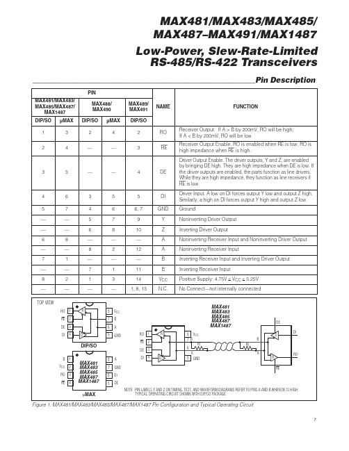
MAX481E/MAX483E/MAX485E/MAX487E–MAX491E/MAX1487E
±15kV ESD-Protected, Slew-Rate-Limited, Low-Power, RS-485/RS-422 Transceivers
ABSOLUTE MAXIMUM RATINGS
General Description
The MAX481E, MAX483E, MAX485E, MAX487E– MAX491E, and MAX1487E are low-power transceivers for RS-485 and RS-422 communications in harsh environments. Each driver output and receiver input is protected against ±15kV electro-static discharge (ESD) shocks, without latchup. These parts contain one driver and one receiver. The MAX483E, MAX487E, MAX488E, and MAX489E feature reduced slew-rate drivers that minimize EMI and reduce reflections caused by improperly terminated cables, thus allowing error-free data transmission up to 250kbps. The driver slew rates of the MAX481E, MAX485E, MAX490E, MAX491E, and MAX1487E are not limited, allowing them to transmit up to 2.5Mbps.
MAX4173TEUT-T中文资料

Notebook Computers
Portable/Battery-Powered Systems
Smart Battery Packs/Chargers
Cell Phones
Power-Management Systems
General System/Board-Level Current Monitoring
The combination of three gain versions and a userselectable external sense resistor sets the full-scale current reading. This feature offers a high level of integration, resulting in a simple and compact currentsense solution.
+20V/V (MAX4173T) +50V/V (MAX4173F) +100V/V (MAX4173H) ♦ ±0.5% Full-Scale Accuracy ♦ ±0.3mV Input Offset Voltage (MAX4173T) ♦ 420µA Supply Current ♦ Wide 1.7MHz Bandwidth (MAX4173T) ♦ +3V to +28V Operating Supply ♦ Available in Space-Saving SOT23-6 Package
Typical Operating Circuit
0 TO +28V
VSENSE
+3V TO +28V 0.1µF
nRF401中文手册

表 1. nRF401 主要技术特性
*PWR_UP 管脚间歇供电 占空比 2% 周期 200ms
单位
MHZ
KHz dBm dBm kbit/s
V uA mA uA
定购信息
型号
nRF401-IC nRF401-EVKIT
特性
20pin SSOIC Evaluation kit with nRF401 IC
Sensitivity
@400
.BR=20kbit/s,BER<10-3
Bit rate
ZI
Recommended antenna
port differential impedance
Spurious emission
to +85
最小
典型
最大 单位
2.7
3
5.25
V
0
V
11
mA
8
mA
8
uA
10
DBm
名称 tTR tRT tST tSR tVT tVR
最大延时
3ms 1ms 2ms 3ms 4ms 5ms
条件 连续工作
上电
COPYRIGHT ©2001 ALL RIGHTS RESERVED 迅通科技 TEL: (0451)6349363 6332356 4
433MHZ 单片无线收发芯片
功能描述
真正的单片 FSK 收发芯片 非常少的外围元件 无需进行初始化和配置 不需要对数据进行曼彻斯特编码 最高速率 20Kbps 2 个工作频道 宽工作电压范围 低功耗 待机模式
nRF401
应用领域
报警和安全系统 自动测试系统 家庭自动化控制 遥控装置 车辆安全系统 工业控制 无线通信 电信终端
MAX4466EXK中文资料

5-Pin SC70 (derate 2.5mW/°C above +70°C) .............200mW 5-Pin SOT23 (derate 7.1mW/°C above +70°C) ...........571mW
ELECTRICAL CHARACTERISTICS
(VCC = +5V, VCM = 0, VOUT = VCC/2, RL = ∞ to VCC/2, SHDN = GND (MAX4467/MAX4468 only). TA = TMIN to TMAX, unless otherwise noted. Typical values specified at TA = +25°C.) (Note 1)
TOP VIEW
IN+ 1
5 VCC
MAX4465 GND 2 MAX4466
IN- 3
4 OUT
SC70/SOT23 Pin Configurations continued at end of data sheet.
Rail-to-Rail is a registered trademark of Nippon Motorola, Ltd.
Features
o +2.4V to +5.5V Supply Voltage Operation
o Versions with 5nA Complete Shutdown Available (MAX4467/MAX4468)
MAX1722EZK-T中文资料
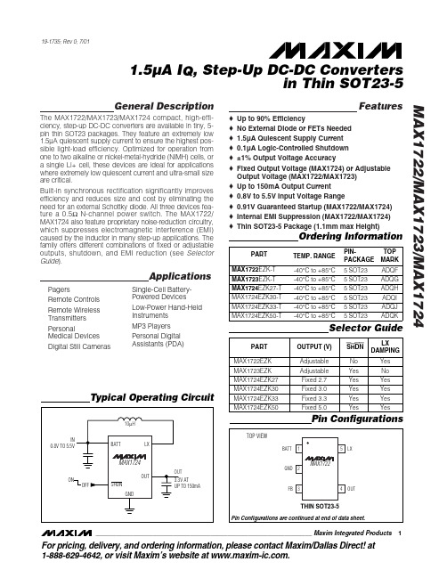
MAX1722
FB 3
4
OUT
THIN SOT23-5
Pin Configurations are continued at end of data sheet.
________________________________________________________________ Maxim Integrated Products
元器件交易网
19-1735; Rev 0; 7/01
1.5µA IQ, Step-Up DC-DC Converters in Thin SOT23-5
General Description
The MAX1722/MAX1723/MAX1724 compact, high-efficiency, step-up DC-DC converters are available in tiny, 5pin thin SOT23 packages. They feature an extremely low 1.5µA quiescent supply current to ensure the highest possible light-load efficiency. Optimized for operation from one to two alkaline or nickel-metal-hydride (NiMH) cells, or a single Li+ cell, these devices are ideal for applications where extremely low quiescent current and ultra-small size are critical. Built-in synchronous rectification significantly improves efficiency and reduces size and cost by eliminating the need for an external Schottky diode. All three devices feature a 0.5Ω N-channel power switch. The MAX1722/ MAX1724 also feature proprietary noise-reduction circuitry, which suppresses electromagnetic interference (EMI) caused by the inductor in many step-up applications. The family offers different combinations of fixed or adjustable outputs, shutdown, and EMI reduction (see Selector Guide). o o o o o o o o o o o
美国Eaton公司产品说明书:Eaton PDG23G0040TFFK电解型防护电路保护器

Eaton PDG23G0040TFFKEaton Power Defense molded case circuit breaker, Globally Rated, Frame 2, Three Pole, 40A, 35kA/480V, T-M (Fxd-Fxd) TU, Standard Terminals Line Only (PDG2X3T100)Eaton Power Defense molded case circuit breakerPDG23G0040TFFK 78667989305088.9 mm 152.4 mm 104.6 mm 1.82 kg Eaton Selling Policy 25-000, one (1) year from the date of installation of theProduct or eighteen (18) months from thedate of shipment of the Product,whichever occurs first.RoHS Compliant IEC 60947-2UL 489CSACCC MarkedProduct NameCatalog Number UPCProduct Length/Depth Product Height Product Width Product Weight WarrantyCompliancesCertifications40 AComplete breaker 2Three-polePD2 Global Class A T-M (Fxd-Fxd) TU600 Vac600 VStandard Terminals Line Only35 kAIC at 480 Vac 25 kAIC Icu/ 20 kAIC Ics/ 52.5 kAIC Icm @480V Brazil (IEC) 35 kAIC @480V (UL) 65 kAIC @240V (UL)30 kAIC Icu/ 22.5 kAIC Ics/ 63 kAIC Icm @440V (IEC) 8 kAIC Icu/ 4 kAIC Ics/ 16.8 kAIC Icm @690V (IEC)20 kAIC Icu/ 15/13 kAIC Ics/ 42 kAIC Icm @525V South Africa (IEC)10 kAIC Icu @250 Vdc36 kAIC Icu/ 36 kAIC Ics/ 75.6 kAIC Icm @380-415V (IEC) 18 kAIC @600V (UL/CSA)55 kAIC Icu/ 55 kAIC Ics/ 121 kAIC Icm @240V (IEC) 10 kAIC Icu @125 VdcEaton Power Defense PDG23G0040TFFK 3D drawing Consulting application guide - molded case circuit breakers Amperage Rating Circuit breaker frame type Frame Number of poles Circuit breaker type Class Trip Type Voltage rating Voltage rating - max TerminalsInterrupt rating Interrupt rating range3D CAD drawing packageApplication notesBrochuresPower Defense technical selling bookletPower Defense molded case circuit breaker selection posterPower Defense brochurePower Defense molded case circuit breakers - Frame 2 product aid Certification reportsEU Declaration of Conformity - Power Defense molded case circuit breakersPDG4 CCC certificationPDG4 CB reportPower Defense Declaration concerning California’s Proposition 65PDG2 CB reportInstallation instructionsPower Defense Frame 2 tunnel terminal (aluminum), 50A, 3 pole instructions - IL012236EN H03Power Defense Frame 1 IEC and Frame 2 Rotary Mechanism with NFPA Handle Attachment Instructions (IL012260EN).pdfPower Defense Frame 2 tunnel terminal kits - PDG2X1TA225K instructions- IL012239EN H01Power Defense Frame 2 Direct Rotary Handle Assy With Interlock Version Instructions (IL012138EN).pdfPower Defense Frame 2 screw terminal_end cap kit, 225A, 3 pole instructions - IL012258EN H01Power Defense Frame 2 global terminal shield, 3 pole - IL012330EN Power Defense Frame 2/3/4/5/6 voltage neutral sensor module wiring instructions – IL012316ENPower Defense Frame 2 shunt trip UVR instructions - IL012130EN Power Defense Frame 2 clamp terminal (steel), 20A, 3 pole instructions - IL012246EN H03Power Defense Frame 2 PDG2 and PDC(E)9 breaker instructions -IL012106ENPower Defense Frame 2 multi wire connector kit -PDG2X3(2)(4)TA2256W instructions - IL012242EN H01Power Defense Frame 2 tunnel terminal (aluminum), 150A, 3 pole instructions - IL012238EN H03Power Defense Frame 2 locking devices and handle block instructions - IL012149ENPower Defense Frame 1-2-3-4 IP door barrier assembly instructions -IL012278ENPower Defense Frame 2 handle mech direct rotary handle instructions - IL012134ENPower Defense Frame 2 handle mech variable depth rotary handle instructions - IL012136ENPower Defense Frame 2 multi wire connector kit -PDG2X3(2)(4)TA2253W instructions - IL012243EN H01Power Defense Frame 2 terminal kit - PDG2X3(2)(4)TA225RF instructions - IL012245EN H01Power Defense Frame 2 box terminal (steel), 100A, 3 pole instructions - IL012234EN H03Power Defense Frame 2 tunnel terminal (aluminum), 100A, 3 pole instructions - IL012237EN H03Power Defense Frame 2 box terminal (aluminum), 225A, 3 pole instructions - IL012235EN H03Power Defense Frame 2 terminal kit - PDG2X3(2)(4)TA150RF instructions - IL012244EN H01Installation videosPower Defense Frame 2 Locking Devices and Handle Block Animated Instructions.pdf.rhPower Defense Frame 2 TMTU Aux, Alarm, ST and UVR Animated Instructions.rhPower Defense Frame 2 Bell Alarm with PXR Animated Instructions.pdf.rh Power Defense Frame 2 withTMTU, Shunt Trip_UVR Animated Instructions.rhPower Defense Frame 2 Handle Mech Variable Depth Rotary Handle Animated Instructions.rhMultimediaPower Defense Frame 3 Variable Depth Rotary Handle Mechanism Installation How-To VideoPower Defense Frame 2 Direct Rotary Handle Mechanism Installation How-To VideoPower Defense Frame 2 Variable Depth Rotary Handle Mechanism Installation How-To VideoPower Defense Frame 2 Aux, Alarm, Shunt Trip, and UVR How-To Video Power Defense Frame 5 Trip Unit How-To VideoPower Defense molded case circuit breakersEaton Power Defense for superior arc flash safetyPower Defense BreakersPower Defense Frame 6 Trip Unit How-To VideoSpecifications and datasheetsEaton Specification Sheet - PDG23G0040TFFKTime/current curvesPower Defense time current curve Frame 2 - PD2Warranty guidesSelling Policy 25-000 - Distribution and Control Products and ServicesEaton Corporation plc Eaton House30 Pembroke Road Dublin 4, Ireland © 2023 Eaton. All Rights Reserved. Eaton is a registered trademark.All other trademarks areproperty of their respectiveowners./socialmediaMolded case and low-voltage power circuit breaker health Single and double break MCCB performance revisited Intelligent circuit protection yields space savingsMaking a better machineSafer by design: arc energy reduction techniques Molded case and low-voltage breaker healthWhite papers。
MAX3490摘出资料(部分中文)
MAX3488, MAX3490,MAX3491 功能,全双工通信,而 MAX3483, MAX3485, MAX3486是专为半双工通信。
单一的电源供应,没有电荷注入;具有+ 5V 逻辑电源互操作;最大偏斜为 8ns ; 2ns 低电流掉电模式;共模输入电压范围:—7〜+ 12V ,总线上允许多达 32个收发器;全双工和半双工版本;具有电流限制和热 关机驱动器过载保护驱动器具有短路电流限制和对功耗过大的保护,热关断电路,驱动器输岀置于高阻抗状态。
接收器输入具 有故障安全功能,保证逻辑高输岀,如果两个输入端开路。
选择MAX3490做RS-422,下图为 MAX3490引脚图1 ——VCC2―― RO 接收器输出 3―― DI 驱动器输入 4 ——GND 5 ---- Y 同相驱动器输出 6 ---- Z 反相驱动器输出 7 ---- B反相接收器输入8——A 同相接收器输入保证数据传输速率(Mbps ) 10电源电压(V ) to 半/全双工 全双工摆率限制 无 驱动器/接收器使 无 关断电流(NA )关断时无引脚数8频率大,高频谐波明显MAX3490没有接收器发送器使能,控制逻辑如下图Dences 宙Rhouf Receiver/Driver Enable(MAX3488/MAX349a}T^ble 3. Transmitting T^able 4. ReceivingMAX3490 (无RE 、DE 引脚)绝对最大额定值如下图:IN^UTOUTPUTSDI zY 1 D 1 □1INPUTSOUTPUTA. 6 RO *D.2V1 <-a.2v0 Inputs Open1□IP/SOE L叵叵DABSOLUTE MAXIMUM RATINGSS U P P 卜F \ 01 ^3 9 e l\/ kill ■ ■ ■ ■ ■■!■■■■■■ iri ■ ■ ■ ■ ■ ■ ■ ■ ■ ■ ■ ■■ ■ ■ ■ ■ ■ i ■ ■ ■ r ■ ■ ■ ■ ■ ■ ■Control IrpiJ ValLage (RE, D£) ............... .......... ............... -0.3V ta 7V□rtvsr Inpul Voltage (6l).............. .......... .......... ............... -0.3Vtn 7VOnvar Output VcItaQ* (A,気V, ZX - ......................... -7J5V to12.SVftccer^CF Input VaKagc |A, B) . -7.5V to )2 5VReceiver Ojtput Voltage (RO) . . -O.3Vto (Vcc * 0 3V)Gontinucus Power g$ipmTk?n (T R= +70芒|各Pin Pi/Mc DIP 忖申rate 9 09mWU above +70© 72?mW8-Pin SO (<1HW 5 aarrrtVy «bove +7C P C), 471mW14-Rn Plastic DlP(de<m© 10mW fl C above +70忙》... HOOtrMf14-Rn SO (deia1^ fl.SSmW.^C abaw +70*C> __________ UUJllMfOperating Temperalur?MAXU C .............. ......... *........ ... ..................... -.Ot:to +7[TCMAX3d_ _E__”…lh.. “一,. ,.H.…““-“,-H.⑷乜B +85\:Storage Temperafur? Range lo +16[yCbead Tempeiature [wldering lOlMC)..................................... +XD*CMAX3490驱动器的开关特性如下图:DRIVER SWITCHING CHARACTERISTICS-MAX3465h MAX14$0, and MAX3491ri^E:» 3.3M a T*w *25*CJPARAMtFER CONCilTICNS m TVP MA 9(UNITSDrrwf OHtreftfiii OdljMjt Del叩g■ Sdll, Figure 7 122M mDrvcr Wfe-oEiii Ckrlp ui T M7»C r Time hno良L * fiOtl, Flpm 71&25mEtr p临他n M■丫LCfflMCHHiah Lrvtl IpiLM R L * 37(1. F4l/*a T2235m轉、ion Delay Hl0hi&-Lew Leveli IpML R. - ZTflFiflWWE■Jr22 35tp L n - iPHitl □越g*曲m Dtt&Ff吕的却iH^ie S- IPDS R.fc• 27n, FipL<eS E mDRIVER OUTPUT ENABLEJOIS^BLE TIMES {IWS-iflS'IMLW3-431 聞切Dmw CXJtput tnable r me I Q L OW LE^el tfZL Ri= 110SL f^FLFa 10 45 M OEDiwci" OulpiJl EiwN? Trne tg High Len el S FZH Ri ■ 110(1 钿ure $ 45raDrw CMp讥04»^le Time tom Migih Level fi t* 11(X1. F»flL*t940 to POriw D・*l・ Tim from LwLwi tpLE R L* 11IMI. i&40 BO mDTM< dip Lit Errtb^A Tiffii Au墟电叭旳Lx L#v4l tm Rl ■匚如i 10<8W gm 他Qrta&r ErrtBifi Titre frw 电靜©询|a H(;h 4PCH R; - 1inni FigiLiraS®o r»MAX3490CPA(TCto +70'Q8 Ptasttc DIPMAX349OCSA(TCt口+7D B C\8 SOMAX3490C/D crcto+70e c \Dice'MAX349OEPA-4(rc to +85X8 Plastic DIPMAX349OESA■40X10+9598 SOMAX3490引脚配置与典型工作电路,如下图|l巒4e 2 MAA J4ML JWAJC3啲Pin 8 两#挪询事呵Typ"C^ uftMOTE AEANODE O 8LXF砂*师悶ZKSQW诂沖盟F训卜皿咻斥$钵自Ncrv^OfU MAX3490封装尺寸L -15^ Plastic DIPPLASTIC DU AL-IN-LINE PACKAGE(0.300 in.)DIM [HOMES MLLlWETESS MIN MAA MIN MAXA a 200A1ocn&-■"20 12& C 175 3104-iS *3 0D5& Q0» 1.402W0.01S a 022 041 OKoo^ 1 MC DQOB0 0120200 30 &1D0Q&0 09001328E0.300 0 925 A2A E10咖0 310dia7VT e OJOO■■eA D.3H)■*tB Q4P0 10 16 L 0 IU a iso 2923J1 PINSMCHES MJJME1TER3-MN NUM MNI MAXa 0 3430 w BM 891 0140^3513-6719-43 ET lir o.-«Q -B51: 911&.43 010MBS 0i1522 4B 23.24 020 101S104535742454□24 1 14H2B52S DE37 13。
西门子微机综合保护装置介绍

Page 1哈尔滨光宇电气自动化有限公司公司介绍Page 2哈尔滨光宇电气自动化有限公司主要产品CL2000 变电站、火电站、水电站综合自动化系统CL2000 电网调度自动化系统CL2000 低压微机综合保护器高频开关直流电源高精度零序电流互感器及高精度电流互感器西门子微机综合保护装置系统集成Page 41.西门子电力自动化业务介绍2.西门子第 代微机综合保护装置SIPROTEC 4 总体介绍3. 西门子微机综合保护装置调试软件DIGSI 4 总体介绍4. 西门子第 代微机综合保护装置SIPROTEC 4 7SJ6X介绍5. 西门子第 代微机综合保护装置SIPROTEC 4 7UT6x介绍6. 西门子第 代微机综合保护装置SIPROTEC 4 7SD610介绍主要介绍内容Page 51.西门子电力自动化业务介绍2.西门子第 代微机综合保护装置SIPROTEC 4 总体介绍3. 西门子微机综合保护装置调试软件DIGSI 4 总体介绍4. 西门子第 代微机综合保护装置SIPROTEC 4 7SJ6X介绍5. 西门子第 代微机综合保护装置SIPROTEC 4 7UT6x介绍6. 西门子第 代微机综合保护装置SIPROTEC 4 7SD610介绍主要介绍内容Page 6Siemens:代表可靠性reliabilityGermanyEurope excl. GermanyAmericasAsia-PacificOthersEmployeesinthousands2000040000600008000050020030040010010000084/8589/9094/9599/0004/05 Sales in millionsof euros由Werner von Siemens创建于1847年Siemens今天已成为最成功的跨国公司之一公司现状2005年10月统计数据461000 名员工754.45亿欧元年销售额在190多个国家设立分公司/机构Page 7Siemens Power Transmission and Distribution PTD: 输配电集团PTD业务范围能源自动化EnergyAutomationPower transformers distributiontransformerswithoilorcast-resininsulation网控系统能源交易系统Networkconsulting maintenance repairand meterservices继电保护和变电站综合自动化系统Components switchgearand turnkeyprojectsforAC and DC powertechnology forpowertransmission≤52kVComponents switchgearand turnkeyprojectsforAC and DC powertechnology forpowertransmission 52kVPage 8全球范围第一名No.121 市场份额3500 职员业务覆盖60多个国家于2004年获得EFQM的特殊奖励Siemens 输配电能源自动化/PTD EA:市场现状继电保护能源自动化系统通讯大型控制系统研发生产能源自动化/EnergyAutomationPage 9西门子电力自动化有限公司Siemens Power Automation Ltd. SPA给中国客户带来能源自动化的创新技术提供全系列的产品 保护、变电站综合自动化系统、电能计量及能源管理系统。
MEMORY存储芯片MAX491EESD+T中文规格书
μMAX
8 VCC 7B 6A 5 GND
8A
RO 1
R
RE 2
DE 3
DI 4 D
8 VCC 7B
Rt 6
A
5 GND
MAX481 MAX483 MAX485 MAX487 MAX1487
DE
DI D B Rt
A R
RO
7 GND
RE
6 DI
5 DE
NOTE: PIN LABELS Y AND Z ON TIMING, TEST, AND WAVEFORM DIAGRAMS REFER TO PINS A AND B WHEN DE IS HIGH. TYPICAL OPERATING CIRCUIT SHOWN WITH DIP/SO PACKAGE.
MAX481/MAX483/MAX485/ MAX487–MAX491/MAX1487
Low-Power, Slew-Rate-Limited RS-485/RS-422 Transceivers
______________________________________________________________Pin Description
Figure 1. MAX481/MAX483/MAX485/MAX487/MAX1487 Pin Configuration and Typical Operating Circuit
7
MAX481/MAX483/MAX485/ MAX487–MAX491/MAX1487
Low-Power, Slew-Rate-Limited RS-485/RS-422 Transceivers
8
__________Applications Information
莫加 EDS-G4014 系列全球通信网络设备说明书

EDS-G4014Series8G+62.5GbE-port full Gigabit managed Ethernet switchesFeatures and Benefits•Developed according to the IEC62443-4-1and compliant with the IEC62443-4-2industrial cybersecurity standards•Turbo Ring and Turbo Chain(recovery time<50ms@250switches),andRSTP/STP for network redundancy•Wide range of power input options for flexible deployment•Compact and flexible housing design to fit into confined spaces•Supports MXstudio for easy,visualized industrial network management•Increased bandwidth capabilities with fiber SFP slots supporting up to2.5GbpsCertificationsIntroductionThe EDS-G4014Series is equipped with eight Gigabit Ethernet ports and six2.5Gbps fiber-optic ports,making it ideal for upgrading an existing network to Gigabit speed or building a new full Gigabit backbone.Gigabit transmission speed increases bandwidth for higher performance and can transfer large amounts of triple-play services across a network quickly.Redundant Ethernet technologies such as Turbo Ring,Turbo Chain,and RSTP/STP increase the reliability of your system and improve the availability of your network backbone.The EDS-G4014Series is designed specifically for demanding applications such as video and process monitoring,ITS,and DCS systems,all of which can benefit from a scalable backbone.The EDS-G4014Series is compliant with the IEC62443-4-2and IEC62443-4-1Industrial Cybersecurity certifications,which cover both product security and secure development life-cycle requirements,helping our customers meet the compliance requirements of secure industrial network design.SpecificationsEthernet Interface10/100/1000BaseT(X)Ports(RJ45connector)8Auto MDI/MDI-X connectionAuto negotiation speedFull/Half duplex mode100/1000/2500BaseSFP Ports41000/2500BaseSFP Ports2Standards IEEE802.3for10BaseTIEEE802.3u for100BaseT(X)IEEE802.3ab for1000BaseT(X)IEEE802.3z for1000BaseXIEEE802.3bz for2.5GBaseXIEEE802.3x for flow controlIEEE802.3ad for Port Trunk with LACPIEEE802.1Q for VLAN TaggingIEEE802.1D-2004for Spanning Tree ProtocolIEEE802.1w for Rapid Spanning Tree ProtocolIEEE802.1p for Class of ServiceIEEE802.1X for authenticationEthernet Software FeaturesFilter GMRP,GVRP,GARP,802.1Q VLAN,IGMP Snooping v1/v2/v3,IGMP Querier Management IPv4/IPv6,Flow control,Back Pressure Flow Control,DHCP Server/Client,ARP,RARP,LLDP,Port Mirror,Linkup Delay,SMTP,SNMP Trap,SNMP Inform,SNMPv1/v2c/v3,RMON,TFTP,SFTP,HTTP,HTTPS,Telnet,Syslog,Private MIBMIB P-BRIDGE MIB,Q-BRIDGE MIB,IEEE8021-SPANNING-TREE-MIB,IEEE8021-PAE-MIB,IEEE8023-LAG-MIB,LLDP-EXT-DOT1-MIB,LLDP-EXT-DOT3-MIB,SNMPv2-MIB,RMON MIB Groups1,2,3,9Redundancy Protocols STP,RSTP,Turbo Ring v2,Turbo Chain,Ring Coupling,Dual-Homing,LinkAggregation,MSTPSecurity Broadcast storm protection,Rate Limit,Trust access control,Static Port Lock,MACSticky,HTTPS/SSL,SSH,RADIUS,TACACS+,Login and Password Policy,Accesscontrol listTime Management SNTP,NTP Server/Client,NTP AuthenticationProtocols IPv4/IPv6,TCP/IP,UDP,ICMP,ARP,RARP,TFTP,DNS,NTP Client,DHCP Server,DHCP Client,802.1X,QoS,HTTPS,HTTP,Telnet,SMTP,SNMPv1/v2c/v3,RMON,SyslogSwitch PropertiesMAC Table Size16KJumbo Frame Size9.216KBMax.No.of VLANs256VLAN ID Range VID1to4094IGMP Groups512Priority Queues4Packet Buffer Size1MBLED InterfaceLED Indicators PWR1,PWR2,STATE,FAULT,MSTR/HEAD,CPLR/TAIL,SYNCSerial InterfaceConsole Port RS-232(TxD,RxD,GND),8-pin RJ45(115200,n,8,1)USB InterfaceUSB Connector USB Type A(Reserved)Input/Output InterfaceAlarm Contact Channels1,Relay output with current carrying capacity of1A@24VDCDigital Input Channels1Digital Inputs+13to+30V for state1-30to+3V for state0Max.input current:8mAButtons Reset buttonDIP Switch ConfigurationDIP Switches Turbo Ring,Master,Coupler,ReservePower ParametersConnection2removable4-contact terminal block(s)Pre-installed Power Module-LV/-LV-T models:PWR-100-LV-HV/-HV-T models:PWR-105-HV-INote The EDS-G4014Series supports modular power supplies.The model names and powerparameters are determined by the installed power module.For example:EDS-G4014-6QGS-T+PWR-100-LV=EDS-G4014-6QGS-LV-TEDS-G4014-6QGS-T+PWR-105-HV-I=EDS-G4014-6QGS-HV-TIf you install a different power module,refer to the specifications of the correspondingmodel.For example,if you replace the power module of the EDS-G4014-6QGS-LV-Twith the PWR-105-HV-I,refer to the specifications of the EDS-G4014-6QGS-HV-T. Input Voltage-LV/-LV-T models:12/24/48VDC,Redundant dual inputs-HV/-HV-T models:110/220VDC/VAC,Single inputOperating Voltage-LV/-LV-T models:9.6to60VDC-HV/-HV-T models:88to300VDC,85to264VACInput Current-LV/-LV-T models:12-48VDC,1.50-0.40A or24VDC,0.70A-HV/-HV-T models:110-220VAC,50-60Hz,0.30-0.20A or110-220VDC,0.30-0.20A Power Consumption(Max.)EDS-G4014-6QGS-LV(-T)models:14.91WEDS-G4014-6QGS-HV(-T)models:17.32WOverload Current Protection SupportedReverse Polarity Protection SupportedPhysical CharacteristicsIP Rating IP40Dimensions55x140x122.5mm(2.17x5.51x4.82in)Weight846g(1.87lb)Installation DIN-rail mounting,Wall mounting(with optional kit)Housing MetalEnvironmental LimitsOperating Temperature Standard Models:-10to60°C(14to140°F)Wide Temp.Models:-40to75°C(-40to167°F)Ambient Relative Humidity5to95%(non-condensing)Standards and CertificationsIndustrial Cybersecurity IEC62443-4-1IEC62443-4-2Safety UL61010-2-201,EN62368-1(LVD)EMC EN55032/35,EN61000-6-2/-6-4EMI CISPR32,FCC Part15B Class AEMS IEC61000-4-2ESD:Contact:8kV;Air:15kVIEC61000-4-3RS:80MHz to1GHz:20V/mIEC61000-4-4EFT:Power:4kV;Signal:4kVIEC61000-4-5Surge:Power:4kV;Signal:4kVIEC61000-4-6CS:10VIEC61000-4-8PFMFMaritime-LV/-LV-T models:DNV,ABS,NK,LRVibration IEC60068-2-6Shock IEC60068-2-27Freefall IEC60068-2-32Railway EN50121-4Traffic Control NEMA TS2Power Substation IEC61850-3,IEEE1613Class1Hazardous Locations Class I Division2,ATEX,IECExMTBFTime EDS-G4014-6QGS-LV/LV-T models:994,797hrsEDS-G4014-6QGS-HV/HV-T models:487,613hrsWarrantyWarranty Period5yearsDetails See /warrantyPackage ContentsDevice1x EDS-G4014Series switchDocumentation1x quick installation guide1x product notice,Simplified Chinese1x product certificates of quality inspection,Simplified Chinese1x warranty cardDimensionsOrdering InformationEDS-G4014-6QGS-LV8429.6to60VDC PWR-100-LV-10to60°C EDS-G4014-6QGS-LV-T8429.6to60VDC PWR-100-LV-40to75°CEDS-G4014-6QGS-HV84288to300VDC,85to264VACPWR-105-HV-I-10to60°CEDS-G4014-6QGS-HV-T84288to300VDC,85to264VACPWR-105-HV-I-40to75°CAccessories(sold separately)SFP ModulesSFP-1GEZXLC SFP module with11000BaseEZX port with LC connector for110km transmission,0to60°C operatingtemperatureSFP-1GEZXLC-120SFP module with11000BaseEZX port with LC connector for120km transmission,0to60°C operatingtemperatureSFP-1GLHLC SFP module with11000BaseLH port with LC connector for30km transmission,0to60°C operatingtemperatureSFP-1GLHXLC SFP module with11000BaseLHX port with LC connector for40km transmission,0to60°C operatingtemperatureSFP-1GLSXLC SFP module with11000BaseLSX port with LC connector for1km/2km transmission,0to60°Coperating temperatureSFP-1GLXLC SFP module with11000BaseLX port with LC connector for10km transmission,0to60°C operatingtemperatureSFP-1GSXLC SFP module with11000BaseSX port with LC connector for300m/550m transmission,0to60°Coperating temperatureSFP-1GZXLC SFP module with11000BaseZX port with LC connector for80km transmission,0to60°C operatingtemperatureSFP-1GLHLC-T SFP module with11000BaseLH port with LC connector for30km transmission,-40to85°C operatingtemperatureSFP-1GLHXLC-T SFP module with11000BaseLHX port with LC connector for40km transmission,-40to85°Coperating temperatureSFP-1GLSXLC-T SFP module with11000BaseLSX port with LC connector for1km/2km transmission,-40to85°Coperating temperatureSFP-1GLXLC-T SFP module with11000BaseLX port with LC connector for10km transmission,-40to85°C operatingtemperatureSFP-1GSXLC-T SFP module with11000BaseSX port with LC connector for300m/550m transmission,-40to85°Coperating temperatureSFP-1GZXLC-T SFP module with11000BaseZX port with LC connector for80km transmission,-40to85°C operatingtemperatureSFP-1G10ALC WDM-type(BiDi)SFP module with11000BaseSFP port with LC connector for10km transmission;TX1310nm,RX1550nm,0to60°C operating temperatureSFP-1G10BLC WDM-type(BiDi)SFP module with11000BaseSFP port with LC connector for10km transmission;TX1550nm,RX1310nm,0to60°C operating temperatureSFP-1G20ALC WDM-type(BiDi)SFP module with11000BaseSFP port with LC connector for20km transmission;TX1310nm,RX1550nm,0to60°C operating temperatureSFP-1G20BLC WDM-type(BiDi)SFP module with11000BaseSFP port with LC connector for20km transmission;TX1550nm,RX1310nm,0to60°C operating temperatureSFP-1G40ALC WDM-type(BiDi)SFP module with11000BaseSFP port with LC connector for40km transmission;TX1310nm,RX1550nm,0to60°C operating temperatureSFP-1G40BLC WDM-type(BiDi)SFP module with11000BaseSFP port with LC connector for40km transmission;TX1550nm,RX1310nm,0to60°C operating temperatureSFP-1G10ALC-T WDM-type(BiDi)SFP module with11000BaseSFP port with LC connector for10km transmission;TX1310nm,RX1550nm,-40to85°C operating temperatureSFP-1G10BLC-T WDM-type(BiDi)SFP module with11000BaseSFP port with LC connector for10km transmission;TX1550nm,RX1310nm,-40to85°C operating temperatureSFP-1G20ALC-T WDM-type(BiDi)SFP module with11000BaseSFP port with LC connector for20km transmission;TX1310nm,RX1550nm,-40to85°C operating temperatureSFP-1G20BLC-T WDM-type(BiDi)SFP module with11000BaseSFP port with LC connector for20km transmission;TX1550nm,RX1310nm,-40to85°C operating temperatureSFP-1G40ALC-T WDM-type(BiDi)SFP module with11000BaseSFP port with LC connector for40km transmission;TX1310nm,RX1550nm,-40to85°C operating temperatureSFP-1G40BLC-T WDM-type(BiDi)SFP module with11000BaseSFP port with LC connector for40km transmission;TX1550nm,RX1310nm,-40to85°C operating temperatureSFP-1FELLC-T SFP module with1100Base single-mode with LC connector for80km transmission,-40to85°Coperating temperatureSFP-1FEMLC-T SFP module with1100Base multi-mode,LC connector for2/4km transmission,-40to85°C operatingtemperatureSFP-1FESLC-T SFP module with1100Base single-mode with LC connector for40km transmission,-40to85°Coperating temperatureSFP-2.5GLSLC-T SFP module with12.5GBaseFX port with LC connector,single-mode,for20km transmission,-40to85°C operating temperatureSFP-2.5GSLHLC-T SFP module with12.5GBaseFX port with LC connector,single-mode,for45km transmission,-40to85°C operating temperatureSFP-2.5GMLC-T SFP module with12.5GBaseFX port with LC connector,multi-mode,for170,200,550,600mtransmission,-40to85°C operating temperatureSFP-2.5GSLC-T SFP module with12.5GBaseFX port with LC connector,single-mode,for5km transmission,-40to85°C operating temperaturePower SuppliesHDR-60-2460W/2.5A DIN-rail24VDC power supply,universal85to264VAC or120to370VDC input voltage,-30to70°C operating temperatureNDR-120-24120W/5.0A DIN-rail24VDC power supply,universal90to264VAC or127to370VDC input voltage,-20to70°C operating temperatureNDR-120-48120W/2.5A DIN-rail48VDC power supply,universal90to264VAC or127to370VDC input voltage,-20to70°C operating temperatureNDR-240-48240W/5.0A DIN-rail48VDC power supply,universal90to264VAC or127to370VDC input voltage,-20to70°C operating temperatureMDR-40-24DIN-rail24VDC power supply with40W/1.7A,85to264VAC,or120to370VDC input,-20to70°Coperating temperatureMDR-60-24DIN-rail24VDC power supply with60W/2.5A,85to264VAC,or120to370VDC input,-20to70°Coperating temperature©Moxa Inc.All rights reserved.Updated Nov01,2022.This document and any portion thereof may not be reproduced or used in any manner whatsoever without the express written permission of Moxa Inc.Product specifications subject to change without notice.Visit our website for the most up-to-date product information.。
MAX4130EUK+T,MAX4130EUK+T,MAX4132ESA+,MAX4132EUA+,MAX4131ESA,MAX4131EBT+T, 规格书,Datasheet 资料

MAX4130–MAX4134________________________________________________________________Maxim Integrated Products1For pricing, delivery, and ordering information,please contact Maxim/Dallas Direct!at 1-888-629-4642, or visit Maxim’s website at .General DescriptionThe MAX4130–MAX4134 family of operational amplifiers combines 10MHz gain-bandwidth product and excellent DC accuracy with Rail-to-Rail ®operation at the inputs and outputs. These devices require only 900µA per amplifier, and operate from either a single supply (+2.7V to +6.5V) or dual supplies (±1.35V to ±3.25V) with a common-mode voltage range that extends 250mV beyond V EE and V CC . They are capable of driving 250Ωloads and are unity-gain stable. In addition, the MAX4131/ MAX4133 feature a shutdown mode in which the outputs are placed in a high-impedance state and the supply current is reduced to only 25µA per amplifier.With their rail-to-rail input common-mode range and output swing, the MAX4130–MAX4134 are ideal for low-voltage, single-supply operation. Although the minimum operating voltage is specified at 2.7V, the devices typically operate down to 1.8V. In addition, low offset voltage and high speed make them the ideal signal-conditioning stages for precision, low-voltage data-acquisition systems. The MAX4130 is offered in the space-saving 5-pin SOT23 package. The MAX4131 is offered in the ultra-small 6-bump, 1mm x 1.5mm chip-scale package (UCSP™).________________________ApplicationsBattery-Powered Instruments Portable Equipment Data-Acquisition Systems Signal ConditioningLow-Power, Low-Voltage ApplicationsFeatureso 6-Bump UCSP (MAX4131)o +2.7V to +6.5V Single-Supply Operationo Rail-to-Rail Input Common-Mode Voltage Rangeo Rail-to-Rail Output Voltage Swing o 10MHz Gain-Bandwidth Product o 900µA Quiescent Current per Amplifier o 25µA Shutdown Function (MAX4131/MAX4133)o 200µV Offset Voltageo No Phase Reversal for Overdriven Inputs o Drive 250ΩLoadso Stable with 160pF Capacitive Loads o Unity-Gain StableSingle/Dual/Quad, Wide-Bandwidth, Low-Power,Single-Supply, Rail-to-Rail I/O Op Amps19-1089; Rev 3; 3/03*Dice are specified at T A = +25°C. DC parameters only.Ordering Information continued at end of data sheet.Pin Configurations appear at end of data sheet.Rail-to-Rail is a registered trademark of Nippon Motorola, Ltd.UCSP is a trademark of Maxim Integrated Products, Inc.M A X 4130–M A X 4134Single/Dual/Quad, Wide-Bandwidth, Low-Power,Single-Supply Rail-to-Rail I/O Op Amps 2_______________________________________________________________________________________ABSOLUTE MAXIMUM RATINGSDC ELECTRICAL CHARACTERISTICS(V CC = +2.7V to +6.5V, V EE = 0V, V CM = 0V, V OUT = V CC /2, R L tied to V CC /2, SHDN ≥2V (or open), T A = +25°C , unless otherwise noted.)Stresses beyond those listed under “Absolute Maximum Ratings” may cause permanent damage to the device. These are stress ratings only, and functional operation of the device at these or any other conditions beyond those indicated in the operational sections of the specifications is not implied. Exposure to absolute maximum rating conditions for extended periods may affect device reliability.Supply Voltage (V CC - V EE )...................................................7.5V IN+, IN-, SHDN Voltage...................(V CC + 0.3V) to (V EE - 0.3V)Output Short-Circuit Duration (Note 1).......................Continuous(short to either supply)Continuous Power Dissipation (T A = +70°C)5-Pin SOT23 (derate 7.1mW/°C above +70°C)............571mW 6-Bump UCSP (derate 2.9mW/°C above +70°C).........308mW 8-Pin SO (derate 5.88mW/°C above +70°C)................471mW8-Pin µMAX (derate 4.10mW/°C above +70°C)...........330mW 14-Pin SO (derate 8.00mW/°C above +70°C)..............640mW Operating Temperature RangeMAX413_E__...................................................-40°C to +85°C Maximum Junction Temperature.....................................+150°C Storage Temperature Range.............................-65°C to +160°C Lead Temperature (soldering, 10s).................................+300°C Bump Reflow Temperature .........................................+235°CNote 1:Provided that the maximum package power-dissipation rating is not exceeded.MAX4130–MAX4134Single/Dual/Quad, Wide-Bandwidth, Low-Power,Single-Supply Rail-to-Rail I/O Op AmpsDC ELECTRICAL CHARACTERISTICS (continued)(V CC = +2.7V to +6.5V, V EE = 0V, V CM = 0V, V OUT = V CC /2, R L tied to V CC /2, SHDN ≥2V (or open), T A = +25°C , unless otherwise noted.)DC ELECTRICAL CHARACTERISTICS(V CC = +2.7V to +6.5V, V EE = 0V, V CM = 0V, V OUT = V CC /2, R L tied to V CC /2, SHDN ≥2V (or open), T A = -40°C to +85°C , unlessM A X 4130–M A X 4134Single/Dual/Quad, Wide-Bandwidth, Low-Power,Single-Supply Rail-to-Rail I/O Op Amps 4_______________________________________________________________________________________DC ELECTRICAL CHARACTERISTICS(V CC = +2.7V to +6.5V, V EE = 0V, V CM = 0V, V OUT = V CC /2, R L tied to V CC /2, SHDN ≥2V (or open), T A = -40°C to +85°C , unlessMAX4130–MAX4134Single/Dual/Quad, Wide-Bandwidth, Low-Power,Single-Supply Rail-to-Rail I/O Op Amps_______________________________________________________________________________________5DC ELECTRICAL CHARACTERISTICS (continued)(V CC = +2.7V to +6.5V, V EE = 0V, V CM = 0V, V OUT = V CC /2, R L tied to V CC /2, SHDN ≥2V (or open), T A = -40°C to +85°C , unless otherwise noted.) (Note 2)AC ELECTRICAL CHARACTERISTICSM A X 4130–M A X 4134Single/Dual/Quad, Wide-Bandwidth, Low-Power,Single-Supply, Rail-to-Rail I/O Op Amps 6_______________________________________________________________________________________60-401001k 10k 1M 10M100k 100M GAIN AND PHASE vs. FREQUENCY-20FREQUENCY (Hz)G A I N (d B )02040P H A S E (D E G R E E S )180144720-72-144-180-108-363610860-401001k 10k 1M 10M100k 100MGAIN AND PHASEvs. FREQUENCY (WITH C)-20FREQUENCY (Hz)G A I N (d B )2040P H A S E (D E G R E E S )180144720-72-144-180-108-36361080-100101001k100k1M10M10k 100MPOWER-SUPPLY REJECTIONvs. FREQUENCY-80FREQUENCY (Hz)P S R (d B )-60-40-2001051520253530454050-40-25-105203550658095SHUTDOWN SUPPLY CURRENTvs. TEMPERATURETEMPERATURE (°C)S U P P L Y C U R R E N T (µA )1000.100.011001k100k1M10M10k100MOUTPUT IMPEDANCE vs. FREQUENCYFREQUENCY (Hz)O U T P U T I M P E D A N C E (Ω)1101150800850900950105010001100-40-25-105203550658095SUPPLY CURRENT PER AMPLIFIERvs. TEMPERATURETEMPERATURE (°C)S U P P L Y C U R R E N T (µA )-10-505101520-40-25-105203550658095OUTPUT LEAKAGE CURRENTvs. TEMPERATURETEMPERATURE (°C)L E A K A G E C U R R E N T (µA )Typical Operating Characteristics(V CC = +5V, V EE = 0V, VCM = V CC / 2, T A = +25°C, unless otherwise noted.)-600123456INPUT BIAS CURRENT vs. COMMON-MODE VOLTAGECOMMON-MODE VOLTAGE (V)I N P U T B I A S C U R R E N T (n A )-50-40-30-20-10010203040-60-40-40-25-105203550658095INPUT BIAS CURRENTvs. TEMPERATURETEMPERATURE (°C)I N P U T B I A S C U R R E N T (n A )-200204060MAX4130–MAX4134Single/Dual/Quad, Wide-Bandwidth, Low-Power,Single-Supply, Rail-to-Rail I/O Op Amps_______________________________________________________________________________________712070750600110115OUTPUT VOLTAGE: EITHER SUPPLY (mV)G A I N (d B )30095859080100200500105100400LARGE-SIGNAL GAIN vs. OUTPUT VOLTAGE130-40-25-105203550658095LARGE-SIGNAL GAIN vs. TEMPERATURE90120TEMPERATURE (°C)G A I N (d B )11010085951251151051.21.31.51.41.61.71.81.9-40-25-105203550658095MINIMUM OPERATING VOLTAGEvs. TEMPERATUREM A X 4130/34-21TEMPERATURE (°C)M I N I M U M O P E R A T I N G V O L T A G E (V )Typical Operating Characteristics (continued)(V CC = +5V, V EE = 0V, V CM = V CC / 2, T A = +25°C, unless otherwise noted.)12080859095100105110115-40-25-105203550658095COMMON-MODE REJECTIONvs. TEMPERATURETEMPERATURE (°C)C O M M O N -M ODE R E J E C T I O N (d B )130700600120OUTPUT VOLTAGE: EITHER SUPPLY (mV)G A I N (dB )3001009080100200500110400LARGE-SIGNAL GAIN vs. OUTPUT VOLTAGE12060600110OUTPUT VOLTAGE: EITHER SUPPLY (mV)G A I N (d B )300908070100200500100400LARGE-SIGNAL GAIN vs. OUTPUT VOLTAGE12080-40-25-105203550658095LARGE-SIGNAL GAIN vs. TEMPERATURE90TEMPERATURE (°C)G A I N (d B )105859511511010012070750600110115OUTPUT VOLTAGE: EITHER SUPPLY (mV)G A I N (d B )30095859080100200500105100400LARGE-SIGNAL GAIN vs. OUTPUT VOLTAGE-3.00-2.25-0.75-1.5001.500.752.253.00-40-25-105203550658095INPUT OFFSET VOLTAGE vs. TEMPERATURETEMPERATURE (°C)V O L T A G E (m V )M A X 4130–M A X 4134Single/Dual/Quad, Wide-Bandwidth, Low-Power,Single-Supply, Rail-to-Rail I/O Op Amps 8_______________________________________________________________________________________1408010k 1k 100k 10M 1M CHANNEL SEPARATION vs. FREQUENCYFREQUENCY (Hz)C H A N N E L S E P A R A T I O N (d B )1009013011012010100k10kFREQUENCY (Hz)1001k 0.03000.0050.0100.0150.0200.025 TOTAL HARMONIC DISTORTION AND NOISE vs. FREQUENCYT H D A N D N O I S E (%)0.10.0014.04.44.25.04.84.6TOTAL HARMONIC DISTORTION AND NOISE vs. PEAK-TO-PEAK SIGNAL AMPLITUDEPEAK-TO-PEAK SIGNAL AMPLITUDE (V)T H D + N O I S E (%)0.01INTIME (200ns/div)V O L T A G E (50m V /d i v )OUTMAX4131SMALL-SIGNAL TRANSIENT RESPONSE (NONINVERTING)IN TIME (200ns/div)V O L T A G E (50m V /d i v )OUT MAX4131SMALL-SIGNAL TRANSIENT RESPONSE (INVERTING)A V = -1IN TIME (2µs/div)V O L T A G E (2V/d i v )OUT MAX4131LARGE-SIGNAL TRANSIENT RESPONSE (NONINVERTING)A V = +1INTIME (2µs/div)V O L T A G E (2V /d i v )OUTMAX4131LARGE-SIGNAL TRANSIENT RESPONSE (INVERTING)Typical Operating Characteristics (continued)(V CC = +5V, V EE = 0V, V CM = V CC / 2, T A = +25°C, unless otherwise noted.)1600-40-25-105203550658095MINIMUM OUTPUT VOLTAGEvs. TEMPERATURE20140120TEMPERATURE (°C)V O U T - V E E (m V )100806040050100150200250300-40-25-105203550658095MAXIMUM OUTPUT VOLTAGEvs. TEMPERATURETEMPERATURE (°C)V C C - V O U T (m V )MAX4130–MAX4134Single/Dual/Quad, Wide-Bandwidth, Low-Power,Single-Supply, Rail-to-Rail I/O Op Amps_______________________________________________________________________________________9Figure 1a. Reducing Offset Error Due to Bias Current (Noninverting)Figure 1b. Reducing Offset Error Due to Bias Current (Inverting)M A X 4130–M A X 4134Single/Dual/Quad, Wide-Bandwidth, Low-Power,Single-Supply, Rail-to-Rail I/O Op Amps 10______________________________________________________________________________________Applications InformationRail-to-Rail Input StageDevices in the MAX4130–MAX4134 family of high-speed amplifiers have rail-to-rail input and output stages designed for low-voltage, single-supply opera-tion. The input stage consists of separate NPN and PNP differential stages that combine to provide an input common-mode range that extends 0.2V beyond the supply rails. The PNP stage is active for input volt-ages close to the negative rail, and the NPN stage is active for input voltages near the positive rail. The input offset voltage is typically below 200µV. The switchover transition region, which occurs near V CC / 2, has been extended to minimize the slight degradation in com-mon-mode rejection ratio caused by the mismatch of the input pairs. Their low offset voltage, high band-width, and rail-to-rail common-mode range make these op amps excellent choices for precision, low-voltage data-acquisition systems.Since the input stage switches between the NPN and PNP pairs, the input bias current changes polarity as the input voltage passes through the transition region.Reduce the offset error caused by input bias currents flowing through external source impedances by match-ing the effective impedance seen by each input (Figures 1a, 1b). High source impedances, together with input capacitance, can create a parasitic pole that produces an underdamped signal response. Reducing the input impedance or placing a small (2pF to 10pF)capacitor across the feedback resistor improves response.The MAX4130–MAX4134s ’ inputs are protected from large differential input voltages by 1k Ωseries resistors and back-to-back triple diodes across the inputs (Figure 2). For differential input voltages less than 1.8V,input resistance is typically 500k Ω. For differential input voltages greater than 1.8V, input resistance is approxi-mately 2k Ω. The input bias current is given by the fol-lowing equation:Figure 2. Input Protection CircuitMAX4130–MAX4134Single/Dual/Quad, Wide-Bandwidth, Low-Power,Single-Supply, Rail-to-Rail I/O Op Amps______________________________________________________________________________________11Rail-to-Rail Output StageThe minimum output voltage is within millivolts of ground for single-supply operation where the load is referenced to ground (V EE ). Figure 3 shows the input voltage range and output voltage swing of a MAX4131connected as a voltage follower. With a +3V supply and the load tied to ground, the output swings from 0.00V to 2.90V. The maximum output voltage swing depends on the load, but will be within 150mV of a +3V supply, even with the maximum load (500Ωto ground).Driving a capacitive load can cause instability in most high-speed op amps, especially those with low quies-cent current. The MAX4130–MAX4134 have a high tol-erance for capacitive loads. They are stable with capacitive loads up to 160pF. Figure 4 gives the stable operating region for capacitive loads. Figures 5 and 6show the response with capacitive loads and the results of adding an isolation resistor in series with the output (Figure 7). The resistor improves the circuit ’s phase margin by isolating the load capacitor from the op amp ’s output.INTIME (1µs/div)V O L T A G E (1V /d i v )OUTV CC = 3V, R L = 10k Ω to V EEFigure 3. Rail-to-Rail Input/Output Voltage RangeFigure 4. Capacitive-Load StabilityINTIME (200ns/div)V O L T A G E (50m V /d i v )OUTV CC = 5V R L = 10k Ω C L = 130pFFigure 5. MAX4131 Small-Signal Transient Response with Capacitive Load Figure 6. MAX4131 Transient Response to Capacitive Load with Isolation ResistorINTIME (500ns/div)V O L T A G E (50m V /d i v )OUTV CC = 5V C L = 1000pF R S = 39ΩM A X 4130–M A X 4134Single/Dual/Quad, Wide-Bandwidth, Low-Power,Single-Supply, Rail-to-Rail I/O Op Amps 12______________________________________________________________________________________Power-Up and Shutdown ModeThe MAX4130–MAX4134 amplifiers typically settle with-in 1µs after power-up. Figures 9 and 10 show the out-put voltage and supply current on power-up, using the test circuit of Figure 8.The MAX4131 and MAX4133 have a shutdown option.When the shutdown pin (SHDN ) is pulled low, the sup-ply current drops below 25µA per amplifier and theamplifiers are disabled with the outputs in a high-impedance state. Pulling SHDN high or leaving it float-ing enables the amplifier. In the dual-amplifier MAX4133, the shutdown functions operate indepen-dently. Figures 11 and 12 show the output voltage and supply current responses of the MAX4131 to a shut-down pulse, using the test circuit of Figure 8.Figure 7. Capacitive-Load Driving CircuitFigure 8. Power-Up/Shutdown Test CircuitV CC TIME (5µs/div)V O L T A G E (1V /d i v )OUTFigure 9. Power-Up Output Voltage V CC (1V/div)TIME (5µs/div)I EE(500µA/div)Figure 10. Power-Up Supply CurrentMAX4130–MAX4134Single/Dual/Quad, Wide-Bandwidth, Low-Power,Single-Supply, Rail-to-Rail I/O Op Amps______________________________________________________________________________________13Power Supplies and LayoutThe MAX4130–MAX4134 operate from a single +2.7V to +6.5V power supply, or from dual supplies of ±1.35V to ±3.25V. For single-supply operation, bypass the power supply with a 0.1µF ceramic capacitor in parallel with at least 1µF. For dual supplies, bypass each sup-ply to ground.Good layout improves performance by decreasing the amount of stray capacitance at the op amp ’s inputs and outputs. Decrease stray capacitance by placing external components close to the op amp ’s pins, mini-mizing trace lengths and resistor leads.UCSP Applications InformationFor the latest application details on UCSP construction,dimensions, tape carrier information, PC board tech-niques, bump-pad layout, and the recommended reflow temperature profile, as well as the latest informa-tion on reliability testing results, go to Maxim ’s website at /ucsp and search for the Application Note: UCSP –A Wafer-Level Chip-Scale Package .TIME (1µs/div)OUTFigure 11. Shutdown Output Voltage TIME (1µs/div)Figure 12. Shutdown Enable/Disable Supply CurrentM A X 4130–M A X 4134Single/Dual/Quad, Wide-Bandwidth, Low-Power,Single-Supply, Rail-to-Rail I/O Op Amps 14________________________________________________________________________________________________________________________________________________Pin ConfigurationsMAX4130–MAX4134Single/Dual/Quad, Wide-Bandwidth, Low-Power,Single-Supply, Rail-to-Rail I/O Op Amps______________________________________________________________________________________15Chip InformationOrdering Information (continued)MAX4130 TRANSISTOR COUNT: 170MAX4131 TRANSISTOR COUNT: 170MAX4132 TRANSISTOR COUNT: 340MAX4134 TRANSISTOR COUNT: 680*Dice are specified at T A = +25°C, DC parameters only.Package Information(The package drawing(s) in this data sheet may not reflect the most current specifications. For the latest package outline information,go to /packages .)M A X 4130–M A X 4134Single/Dual/Quad, Wide-Bandwidth, Low-Power,Single-Supply, Rail-to-Rail I/O Op Amps 16______________________________________________________________________________________Package Information (continued)(The package drawing(s) in this data sheet may not reflect the most current specifications. For the latest package outline information,go to /packages .)MAX4130–MAX4134Single/Dual/Quad, Wide-Bandwidth, Low-Power,Single-Supply, Rail-to-Rail I/O Op Amps______________________________________________________________________________________17Package Information (continued)(The package drawing(s) in this data sheet may not reflect the most current specifications. For the latest package outline information,go to /packages .)Maxim cannot assume responsibility for use of any circuitry other than circuitry entirely embodied in a Maxim product. No circuit patent licenses are M A X 4130–M A X 4134Single/Dual/Quad, Wide-Bandwidth, Low-Power,Single-Supply, Rail-to-Rail I/O Op Amps implied. Maxim reserves the right to change the circuitry and specifications without notice at any time.18__________________Maxim Integrated Products, 120 San Gabriel Drive, Sunnyvale, CA 94086 (408) 737-7600©2003 Maxim Integrated ProductsPrinted USAis a registered trademark of Maxim Integrated Products.Package Information (continued)(The package drawing(s) in this data sheet may not reflect the most current specifications. For the latest package outline information,go to /packages .)。
MAXIM MAX4604 MAX4605 MAX4606 说明书

For free samples & the latest literature: , or phone 1-800-998-8800.For small orders, phone 1-800-835-8769.General DescriptionThe MAX4604/MAX4605/MAX4606 quad analog switch-es feature 5Ωmax on-resistance. On-resistance is matched between switches to 0.5Ωmax and is flat (0.5Ωmax) over the specified signal range. Each switch can handle Rail-to-Rail ®analog signals. The off-leakage cur-rent is only 2.5nA max at +85°C. These analog switches are ideal in low-distortion applications and are the pre-ferred solution over mechanical relays in automatic test equipment or in applications where current switching is required. These switches have low power requirements,require less board space, and are more reliable than mechanical relays.The MAX4604 has four normally closed (NC) switches,the MAX4605 has four normally open (NO) switches,and the MAX4606 has two NC and two NO switches.These switches operate from a single supply of +4.5V to +36V or from dual supplies of ±4.5V to ±20V. All dig-ital inputs have +0.8V and +2.4V logic thresholds,ensuring TTL/CMOS logic compatibility when using ±15V supplies or a single +12V supply.ApplicationsReed Relay Replacement PBX, PABX Systems Test EquipmentAudio-Signal Routing Communication SystemsAvionicsFeatureso Low On-Resistance (5Ωmax)o Guaranteed R ON Match Between Channels (0.5Ωmax)o Guaranteed R ON Flatness over Specified Signal Range (0.5Ωmax)o Rail-to-Rail Signal Handlingo Guaranteed ESD Protection > 2000V per Method 3015.7o Single-Supply Operation: +4.5V to +36V Dual-Supply Operation: ±4.5V to ±20V o TTL/CMOS-Compatible Control InputsMAX4604/MAX4605/MAX46065Ω, Quad, SPST, CMOS Analog Switches________________________________________________________________Maxim Integrated Products1Pin Configurations/Functional Diagrams/Truth Tables19-1393; Rev 1; 8/99Ordering Information continued at end of data sheet.Ordering InformationRail-to-Rail is a registered trademark of Nippon Motorola, Ltd.M A X 4604/M A X 4605/M A X 46065Ω, Quad, SPST, CMOS Analog Switches 2_______________________________________________________________________________________ABSOLUTE MAXIMUM RATINGSNote 1:Signals on NC_, NO_, COM_, or IN_ exceeding V+ or V- are clamped by internal diodes. Limit forward-diode current tomaximum current rating.V+ to GND..............................................................-0.3V to +44V V- to GND..............................................................+0.3V to -44V V+ to V-...................................................................-0.3V to +44V V L to GND......................................(DGND - 0.3V) to (V+ + 0.3V)All Other Pins to DGND (Note 1).........(V- - 0.3V) to (V+ + 0.3V) Continuous Current (COM_, NO_, NC_) ........................±100mA Peak Current (COM_, NO_, NC_)(pulsed at 1ms, 10% duty cycle)...............................±300mAContinuous Power Dissipation (T A = +70°C)16-pin Narrow SO (derate 8.70mW/°C above +70°C)....696mW 16-pin Plastic DIP (derate 10.53mW/°C above +70°C)..842mW Operating Temperature RangesMAX460_C_E ......................................................0°C to +70°C MAX460_E_E....................................................-40°C to +85°C Storage Temperature Range.............................-65°C to +160°C Lead Temperature (soldering, 10sec).............................+300°CELECTRICAL CHARACTERISTICS—Dual Supplies(V+ = +15V, V- = -15V, V L = 5V, V IN_H = 2.4V, V IN_L = 0.8V, T A = T MIN to T MAX , unless otherwise noted. Typical values are at T A = +25°C.)Stresses beyond those listed under “Absolute Maximum Ratings” may cause permanent damage to the device. These are stress ratings only, and functional operation of the device at these or any other conditions beyond those indicated in the operational sections of the specifications is not implied. Exposure to absolute maximum rating conditions for extended periods may affect device reliability.MAX4604/MAX4605/MAX46065Ω, Quad, SPST, CMOS Analog Switches_______________________________________________________________________________________3ELECTRICAL CHARACTERISTICS—Dual Supplies (continued)(V+ = +15V, V- = -15V, V L = 5V, V IN_H = 2.4V, V IN_L = 0.8V, T A = T MIN to T MAX , unless otherwise noted. Typical values are T A = +25°C.)M A X 4604/M A X 4605/M A X 46065Ω, Quad, SPST, CMOS Analog Switches 4_______________________________________________________________________________________ELECTRICAL CHARACTERISTICS—Single Supply(V+ = +12V, V- = 0, V L = 5V, V IN_H = 2.4V, V IN_L = 0.8V, T A = T MIN to T MAX , unless otherwise noted. Typical values are at T A = +25°C.)MAX4604/MAX4605/MAX46065Ω, Quad, SPST, CMOS Analog Switches_______________________________________________________________________________________5ELECTRICAL CHARACTERISTICS—Single Supply (continued)(V+ = +12V, V- = 0, V L = 5V, V IN_H = 2.4V, V IN_L = 0.8V, T A = T MIN to T MAX , unless otherwise noted. Typical values are at T A = +25°C.)Note 2:The algebraic convention, where the most negative value is a minimum and the most positive value a maximum, is used inthis data sheet.Note 3:Guaranteed by design.Note 4:∆R ON = R ON(MAX)- R ON(MIN).Note 5:Flatness is defined as the difference between the maximum and minimum value of on-resistance as measured over thespecified analog signal range.Note 6:Leakage parameters are 100% tested at maximum-rated hot temperature and guaranteed by correlation at +25°C.Note 7:Off-isolation = 20log10 [V COM_/ (V NC_or V NO_)], V COM_= output, V NC_or V NO_= input to off switch.Note 8:Between any two switches.Note 9:Leakage testing at single supply is guaranteed by testing with dual supplies.M A X 4604/M A X 4605/M A X 46065Ω, Quad, SPST, CMOS Analog Switches 6_______________________________________________________________________________________Typical Operating Characteristics(T A = +25°C, unless otherwise noted.)2.03.02.54.03.55.04.55.56.56.07.0-20-10-5-1505101520ON-RESISTANCEV COM (V)R O N (Ω)1.52.52.03.53.04.54.05.0-15-50-1051015ON-RESISTANCE vs. V COMAND TEMPERATURE (DUAL SUPPLIES)V COM (V)R O N (Ω)264108121416186931215182124ON-RESISTANCEvs. V COM (SINGLE SUPPLY)V COM (V)R O N (Ω)3.04.54.03.55.05.56.06.57.07.58.0042681012ON-RESISTANCE vs. VCOMAND TEMPERATURE (SINGLE SUPPLY)V COM (V)R O N (Ω)040208060120100140180160200-10-6-4-2-8248610TURN-ON/TURN-OFF TIMEvs. V COMV COM (V)t O N , t O F F (n s )0.0110k 1010.11001k 100k -40-10520-253550100958065ON/OFF-LEAKAGE CURRENTvs. TEMPERATURETEMPERATURE (°C)L E A K A G E (p A )-250-150-200-50-100500100-15-50-1051015CHARGE INJECTION vs. V COMV COM (V)Q (p C )7090801101001301201401601501701012131411151617191820TURN-ON/TURN-OFF TIME vs. SUPPLY VOLTAGEV+, V- (V)t O N , t O F F (n s )8090120110100130140160150170-40-2020406080100TURN-ON/TURN-OFF TIME vs. TEMPERATURETEMPERATURE (°C)t O N , t O F F (n s )MAX4604/MAX4605/MAX46065Ω, Quad, SPST, CMOS Analog Switches_______________________________________________________________________________________7Typical Operating Characteristics (continued)(T A = +25°C, unless otherwise noted.)Pin Description0.010.110k 1011001k 100k -40-10520-253550100958065SUPPLY CURRENT vs. TEMPERATURETEMPERATURE (°C)I +, I - (n A )-10-1000.1100101FREQUENCY RESPONSE-70-90-30-500-60-80-20-40FREQUENCY (MHz)L O S S (d B )-720-450-630-90-270P H A S E (D E G R E E S )M A X 4604/M A X 4605/M A X 46065Ω, Quad, SPST, CMOS Analog Switches8_______________________________________________________________________________________Applications InformationOvervoltage ProtectionProper power-supply sequencing is recommended for all CMOS devices. Do not exceed the absolute maxi-mum ratings, because stresses beyond the listed rat-ings can cause permanent damage to the devices.Always sequence V+ on first, then V-, followed by the logic inputs, NO, or COM. If power-supply sequencing is not possible, add two small signal diodes (D1, D2) in series with supply pins for overvoltage protection (Figure 1). Adding diodes reduces the analog signal range to one diode drop below V+ and one diode drop above V-, but does not affect the devices’ low switch resistance and low leakage characteristics. Device operation is unchanged, and the difference between V+ and V- should not exceed 44V. These protection diodes are not recommended when using a single supply.Off-Isolation at High FrequenciesIn 50Ωsystems, the high-frequency on-response of these parts extends from DC to above 100MHz with a typical loss of -2dB. When the switch is turned off, how-ever, it behaves like a capacitor, and off isolation decreases with increasing frequency. (Above 300MHz,the switch actually passes more signal turned off than turned on.) This effect is more pronounced with higher source and load impedances.Above 5MHz, circuit board layout becomes critical, and it becomes difficult to characterize the response of theswitch independent of the circuit. The graphs shown in the Typical Operating Characteristics were taken using a 50Ωsource and load connected with BNC connec-tors to a circuit board deemed “average;” that is,designed with isolation in mind, but not using strip-line or other special RF circuit techniques. For critical appli-cations above 5MHz, use the MAX440, MAX441, and MAX442, which are fully characterized up to 160MHz.Figure 1. Overvoltage Protection Using External Blocking DiodesFigure 2. Switching-Time Test CircuitMAX4604/MAX4605/MAX46065Ω, Quad, SPST, CMOS Analog Switches_______________________________________________________________________________________9Figure 3. Charge-Injection Test CircuitFigure 4. Off-Isolation Test CircuitFigure 5. Crosstalk Test CircuitM A X 4604/M A X 4605/M A X 46065Ω, Quad, SPST, CMOS Analog Switches 10______________________________________________________________________________________Figure 6. Switch Off-Capacitance Test Circuit Figure 7. Switch On-Capacitance Test CircuitMAX4604/MAX4605/MAX46065Ω, Quad, SPST, CMOS Analog Switches ______________________________________________________________________________________11Chip Information TRANSISTOR COUNT: 100Package InformationOrdering Information (continued)M A X 4604/M A X 4605/M A X 46065Ω, Quad, SPST, CMOS Analog Switches Maxim cannot assume responsibility for use of any circuitry other than circuitry entirely embodied in a Maxim product. No circuit patent licenses are implied. Maxim reserves the right to change the circuitry and specifications without notice at any time.12____________________Maxim Integrated Products, 120 San Gabriel Drive, Sunnyvale, CA 94086 408-737-7600©1999 Maxim Integrated Products Printed USAis a registered trademark of Maxim Integrated Products.Package Information (continued)。
MAX490E

For pricing, delivery, and ordering information,please contact Maxim/Dallas Direct!at 1-888-629-4642, or visit Maxim’s website at .General DescriptionThe MAX481, MAX483, MAX485, MAX487–MAX491, and MAX1487 are low-power transceivers for RS-485 and RS-422 communication. Each part contains one driver and one receiver. The MAX483, MAX487, MAX488, and MAX489feature reduced slew-rate drivers that minimize EMI and reduce reflections caused by improperly terminated cables,thus allowing error-free data transmission up to 250kbps.The driver slew rates of the MAX481, MAX485, MAX490,MAX491, and MAX1487 are not limited, allowing them to transmit up to 2.5Mbps.These transceivers draw between 120µA and 500µA of supply current when unloaded or fully loaded with disabled drivers. Additionally, the MAX481, MAX483, and MAX487have a low-current shutdown mode in which they consume only 0.1µA. All parts operate from a single 5V supply.Drivers are short-circuit current limited and are protected against excessive power dissipation by thermal shutdown circuitry that places the driver outputs into a high-imped-ance state. The receiver input has a fail-safe feature that guarantees a logic-high output if the input is open circuit.The MAX487 and MAX1487 feature quarter-unit-load receiver input impedance, allowing up to 128 MAX487/MAX1487 transceivers on the bus. Full-duplex communi-cations are obtained using the MAX488–MAX491, while the MAX481, MAX483, MAX485, MAX487, and MAX1487are designed for half-duplex applications.________________________ApplicationsLow-Power RS-485 Transceivers Low-Power RS-422 Transceivers Level TranslatorsTransceivers for EMI-Sensitive Applications Industrial-Control Local Area Networks__Next Generation Device Features♦For Fault-Tolerant ApplicationsMAX3430: ±80V Fault-Protected, Fail-Safe, 1/4Unit Load, +3.3V, RS-485 TransceiverMAX3440E–MAX3444E: ±15kV ESD-Protected,±60V Fault-Protected, 10Mbps, Fail-Safe, RS-485/J1708 Transceivers♦For Space-Constrained ApplicationsMAX3460–MAX3464: +5V, Fail-Safe, 20Mbps,Profibus RS-485/RS-422 TransceiversMAX3362: +3.3V, High-Speed, RS-485/RS-422Transceiver in a SOT23 PackageMAX3280E–MAX3284E: ±15kV ESD-Protected,52Mbps, +3V to +5.5V, SOT23, RS-485/RS-422,True Fail-Safe ReceiversMAX3293/MAX3294/MAX3295: 20Mbps, +3.3V,SOT23, RS-855/RS-422 Transmitters ♦For Multiple Transceiver ApplicationsMAX3030E–MAX3033E: ±15kV ESD-Protected,+3.3V, Quad RS-422 Transmitters ♦For Fail-Safe ApplicationsMAX3080–MAX3089: Fail-Safe, High-Speed (10Mbps), Slew-Rate-Limited RS-485/RS-422Transceivers♦For Low-Voltage ApplicationsMAX3483E/MAX3485E/MAX3486E/MAX3488E/MAX3490E/MAX3491E: +3.3V Powered, ±15kV ESD-Protected, 12Mbps, Slew-Rate-Limited,True RS-485/RS-422 TransceiversMAX481/MAX483/MAX485/MAX487–MAX491/MAX1487Low-Power, Slew-Rate-Limited RS-485/RS-422 Transceivers______________________________________________________________Selection Table19-0122; Rev 8; 10/03Ordering Information appears at end of data sheet.M A X 481/M A X 483/M A X 485/M A X 487–M A X 491/M A X 1487Low-Power, Slew-Rate-Limited RS-485/RS-422 Transceivers 2_______________________________________________________________________________________ABSOLUTE MAXIMUM RATINGSSupply Voltage (V CC ).............................................................12V Control Input Voltage (RE , DE)...................-0.5V to (V CC + 0.5V)Driver Input Voltage (DI).............................-0.5V to (V CC + 0.5V)Driver Output Voltage (A, B)...................................-8V to +12.5V Receiver Input Voltage (A, B).................................-8V to +12.5V Receiver Output Voltage (RO).....................-0.5V to (V CC +0.5V)Continuous Power Dissipation (T A = +70°C)8-Pin Plastic DIP (derate 9.09mW/°C above +70°C)....727mW 14-Pin Plastic DIP (derate 10.00mW/°C above +70°C)..800mW 8-Pin SO (derate 5.88mW/°C above +70°C).................471mW14-Pin SO (derate 8.33mW/°C above +70°C)...............667mW 8-Pin µMAX (derate 4.1mW/°C above +70°C)..............830mW 8-Pin CERDIP (derate 8.00mW/°C above +70°C).........640mW 14-Pin CERDIP (derate 9.09mW/°C above +70°C).......727mW Operating Temperature RangesMAX4_ _C_ _/MAX1487C_ A...............................0°C to +70°C MAX4__E_ _/MAX1487E_ A.............................-40°C to +85°C MAX4__MJ_/MAX1487MJA...........................-55°C to +125°C Storage Temperature Range.............................-65°C to +160°C Lead Temperature (soldering, 10sec).............................+300°CDC ELECTRICAL CHARACTERISTICS(V CC = 5V ±5%, T A = T MIN to T MAX , unless otherwise noted.) (Notes 1, 2)Stresses beyond those listed under “Absolute Maximum Ratings” may cause permanent damage to the device. These are stress ratings only, and functional operation of the device at these or any other conditions beyond those indicated in the operational sections of the specifications is not implied. Exposure to absolute maximum rating conditions for extended periods may affect device reliability.VV IN = -7VV IN = 12V V IN = -7V V IN = 12V Input Current (A, B)I IN2V TH k Ω48-7V ≤V CM ≤12V, MAX487/MAX1487R INReceiver Input Resistance -7V ≤V CM ≤12V, all devices except MAX487/MAX1487R = 27Ω(RS-485), Figure 40.4V ≤V O ≤2.4VR = 50Ω(RS-422)I O = 4mA, V ID = -200mV I O = -4mA, V ID = 200mV V CM = 0V-7V ≤V CM ≤12V DE, DI, RE DE, DI, RE MAX487/MAX1487,DE = 0V, V CC = 0V or 5.25VDE, DI, RE R = 27Ωor 50Ω, Figure 4R = 27Ωor 50Ω, Figure 4R = 27Ωor 50Ω, Figure 4DE = 0V;V CC = 0V or 5.25V,all devices except MAX487/MAX1487CONDITIONSk Ω12µA ±1I OZRThree-State (high impedance)Output Current at ReceiverV 0.4V OL Receiver Output Low Voltage 3.5V OH Receiver Output High Voltage mV 70∆V TH Receiver Input Hysteresis V -0.20.2Receiver Differential Threshold Voltage-0.2mA 0.25mA-0.81.01.55V OD2Differential Driver Output (with load)V 2V 5V OD1Differential Driver Output (no load)µA±2I IN1Input CurrentV 0.8V IL Input Low Voltage V 2.0V IH Input High Voltage V 0.2∆V OD Change in Magnitude of Driver Common-Mode Output Voltage for Complementary Output States V 0.2∆V OD Change in Magnitude of Driver Differential Output Voltage for Complementary Output States V 3V OC Driver Common-Mode Output VoltageUNITS MINTYPMAX SYMBOL PARAMETERMAX481/MAX483/MAX485/MAX487–MAX491/MAX1487Low-Power, Slew-Rate-Limited RS-485/RS-422 Transceivers_______________________________________________________________________________________3SWITCHING CHARACTERISTICS—MAX481/MAX485, MAX490/MAX491, MAX1487(V CC = 5V ±5%, T A = T MIN to T MAX , unless otherwise noted.) (Notes 1, 2)DC ELECTRICAL CHARACTERISTICS (continued)(V CC = 5V ±5%, T A = T MIN to T MAX , unless otherwise noted.) (Notes 1, 2)ns 103060t PHL Driver Rise or Fall Time Figures 6 and 8, R DIFF = 54Ω, C L1= C L2= 100pF ns MAX490M, MAX491M MAX490C/E, MAX491C/E2090150MAX481, MAX485, MAX1487MAX490M, MAX491MMAX490C/E, MAX491C/E MAX481, MAX485, MAX1487Figures 6 and 8, R DIFF = 54Ω,C L1= C L2= 100pFMAX481 (Note 5)Figures 5 and 11, C RL = 15pF, S2 closedFigures 5 and 11, C RL = 15pF, S1 closed Figures 5 and 11, C RL = 15pF, S2 closed Figures 5 and 11, C RL = 15pF, S1 closed Figures 6 and 10, R DIFF = 54Ω,C L1= C L2= 100pFFigures 6 and 8,R DIFF = 54Ω,C L1= C L2= 100pF Figures 6 and 10,R DIFF = 54Ω,C L1= C L2= 100pF CONDITIONS ns 510t SKEW ns50200600t SHDNTime to ShutdownMbps 2.5f MAX Maximum Data Rate ns 2050t HZ Receiver Disable Time from High ns 103060t PLH 2050t LZ Receiver Disable Time from Low ns 2050t ZH Driver Input to Output Receiver Enable to Output High ns 2050t ZL Receiver Enable to Output Low 2090200ns ns 134070t HZ t SKD Driver Disable Time from High |t PLH - t PHL |DifferentialReceiver Skewns 4070t LZ Driver Disable Time from Low ns 4070t ZL Driver Enable to Output Low 31540ns51525ns 31540t R , t F 2090200Driver Output Skew to Output t PLH , t PHL Receiver Input to Output4070t ZH Driver Enable to Output High UNITS MIN TYP MAX SYMBOL PARAMETERFigures 7 and 9, C L = 100pF, S2 closed Figures 7 and 9, C L = 100pF, S1 closed Figures 7 and 9, C L = 15pF, S1 closed Figures 7 and 9, C L = 15pF, S2 closedM A X 481/M A X 483/M A X 485/M A X 487–M A X 491/M A X 1487Low-Power, Slew-Rate-Limited RS-485/RS-422 Transceivers 4_______________________________________________________________________________________SWITCHING CHARACTERISTICS—MAX483, MAX487/MAX488/MAX489(V CC = 5V ±5%, T A = T MIN to T MAX , unless otherwise noted.) (Notes 1, 2)SWITCHING CHARACTERISTICS—MAX481/MAX485, MAX490/MAX491, MAX1487 (continued)(V CC = 5V ±5%, T A = T MIN to T MAX , unless otherwise noted.) (Notes 1, 2)3001000Figures 7 and 9, C L = 100pF, S2 closed Figures 7 and 9, C L = 100pF, S1 closed Figures 5 and 11, C L = 15pF, S2 closed,A - B = 2VCONDITIONSns 40100t ZH(SHDN)Driver Enable from Shutdown toOutput High (MAX481)nsFigures 5 and 11, C L = 15pF, S1 closed,B - A = 2Vt ZL(SHDN)Receiver Enable from Shutdownto Output Low (MAX481)ns 40100t ZL(SHDN)Driver Enable from Shutdown toOutput Low (MAX481)ns 3001000t ZH(SHDN)Receiver Enable from Shutdownto Output High (MAX481)UNITS MINTYP MAX SYMBOLPARAMETERtPLH t SKEW Figures 6 and 8, R DIFF = 54Ω,C L1= C L2= 100pFt PHL Figures 6 and 8, R DIFF = 54Ω,C L1= C L2= 100pFDriver Input to Output Driver Output Skew to Output ns 100800ns ns 2000MAX483/MAX487, Figures 7 and 9,C L = 100pF, S2 closedt ZH(SHDN)Driver Enable from Shutdown to Output High2502000ns2500MAX483/MAX487, Figures 5 and 11,C L = 15pF, S1 closedt ZL(SHDN)Receiver Enable from Shutdown to Output Lowns 2500MAX483/MAX487, Figures 5 and 11,C L = 15pF, S2 closedt ZH(SHDN)Receiver Enable from Shutdown to Output Highns 2000MAX483/MAX487, Figures 7 and 9,C L = 100pF, S1 closedt ZL(SHDN)Driver Enable from Shutdown to Output Lowns 50200600MAX483/MAX487 (Note 5) t SHDN Time to Shutdownt PHL t PLH , t PHL < 50% of data period Figures 5 and 11, C RL = 15pF, S2 closed Figures 5 and 11, C RL = 15pF, S1 closed Figures 5 and 11, C RL = 15pF, S2 closed Figures 5 and 11, C RL = 15pF, S1 closed Figures 7 and 9, C L = 15pF, S2 closed Figures 6 and 10, R DIFF = 54Ω,C L1= C L2= 100pFFigures 7 and 9, C L = 15pF, S1 closed Figures 7 and 9, C L = 100pF, S1 closed Figures 7 and 9, C L = 100pF, S2 closed CONDITIONSkbps 250f MAX 2508002000Maximum Data Rate ns 2050t HZ Receiver Disable Time from High ns 25080020002050t LZ Receiver Disable Time from Low ns 2050t ZH Receiver Enable to Output High ns 2050t ZL Receiver Enable to Output Low ns ns 1003003000t HZ t SKD Driver Disable Time from High I t PLH - t PHL I DifferentialReceiver SkewFigures 6 and 10, R DIFF = 54Ω,C L1= C L2= 100pFns 3003000t LZ Driver Disable Time from Low ns 2502000t ZL Driver Enable to Output Low ns Figures 6 and 8, R DIFF = 54Ω,C L1= C L2= 100pFns 2502000t R , t F 2502000Driver Rise or Fall Time ns t PLH Receiver Input to Output2502000t ZH Driver Enable to Output High UNITS MIN TYP MAX SYMBOL PARAMETERMAX481/MAX483/MAX485/MAX487–MAX491/MAX1487Low-Power, Slew-Rate-Limited RS-485/RS-422 Transceivers_______________________________________________________________________________________530002.5OUTPUT CURRENT vs.RECEIVER OUTPUT LOW VOLTAGE525M A X 481-01OUTPUT LOW VOLTAGE (V)O U T P U T C U R R E N T (m A )1.515100.51.02.0203540450.90.1-50-252575RECEIVER OUTPUT LOW VOLTAGE vs.TEMPERATURE0.30.7TEMPERATURE (°C)O U T P U TL O W V O L T A G E (V )500.50.80.20.60.40100125-20-41.5 2.0 3.0 5.0OUTPUT CURRENT vs.RECEIVER OUTPUT HIGH VOLTAGE-8-16M A X 481-02OUTPUT HIGH VOLTAGE (V)O U T P U T C U R R E N T (m A )2.5 4.0-12-18-6-14-10-203.54.5 4.83.2-50-252575RECEIVER OUTPUT HIGH VOLTAGE vs.TEMPERATURE3.64.4TEMPERATURE (°C)O U T P UT H I G H V O L T A G E (V )0504.04.63.44.23.83.01001259000 1.0 3.0 4.5DRIVER OUTPUT CURRENT vs.DIFFERENTIAL OUTPUT VOLTAGE1070M A X 481-05DIFFERENTIAL OUTPUT VOLTAGE (V)O U T P U T C U R R E N T (m A )2.0 4.05030806040200.5 1.5 2.53.5 2.31.5-50-2525125DRIVER DIFFERENTIAL OUTPUT VOLTAGEvs. TEMPERATURE1.72.1TEMPERATURE (°C)D I F FE R E N T I A L O U T PU T V O L T A G E (V )751.92.21.62.01.8100502.4__________________________________________Typical Operating Characteristics(V CC = 5V, T A = +25°C, unless otherwise noted.)NOTES FOR ELECTRICAL/SWITCHING CHARACTERISTICSNote 1:All currents into device pins are positive; all currents out of device pins are negative. All voltages are referenced to deviceground unless otherwise specified.Note 2:All typical specifications are given for V CC = 5V and T A = +25°C.Note 3:Supply current specification is valid for loaded transmitters when DE = 0V.Note 4:Applies to peak current. See Typical Operating Characteristics.Note 5:The MAX481/MAX483/MAX487 are put into shutdown by bringing RE high and DE low. If the inputs are in this state for lessthan 50ns, the parts are guaranteed not to enter shutdown. If the inputs are in this state for at least 600ns, the parts are guaranteed to have entered shutdown. See Low-Power Shutdown Mode section.M A X 481/M A X 483/M A X 485/M A X 487–M A X 491/M A X 1487Low-Power, Slew-Rate-Limited RS-485/RS-422 Transceivers 6___________________________________________________________________________________________________________________Typical Operating Characteristics (continued)(V CC = 5V, T A = +25°C, unless otherwise noted.)120008OUTPUT CURRENT vs.DRIVER OUTPUT LOW VOLTAGE20100M A X 481-07OUTPUT LOW VOLTAGE (V)O U T P U T C U R R E N T (m A )6604024801012140-1200-7-5-15OUTPUT CURRENT vs.DRIVER OUTPUT HIGH VOLTAGE-20-80M A X 481-08OUTPUT HIGH VOLTAGE (V)O U T P U T C U R R E N T (m A )-31-603-6-4-2024-100-40100-40-60-2040100120MAX1487SUPPLY CURRENT vs. TEMPERATURE300TEMPERATURE (°C)S U P P L Y C U R R E N T (µA )20608050020060040000140100-50-2550100MAX481/MAX485/MAX490/MAX491SUPPLY CURRENT vs. TEMPERATURE300TEMPERATURE (°C)S U P P L Y C U R R E N T (µA )257550020060040000125100-50-2550100MAX483/MAX487–MAX489SUPPLY CURRENT vs. TEMPERATURE300TEMPERATURE (°C)S U P P L Y C U R R E N T (µA )257550020060040000125MAX481/MAX483/MAX485/MAX487–MAX491/MAX1487Low-Power, Slew-Rate-Limited RS-485/RS-422 Transceivers_______________________________________________________________________________________7______________________________________________________________Pin DescriptionFigure 1. MAX481/MAX483/MAX485/MAX487/MAX1487 Pin Configuration and Typical Operating CircuitM A X 481/M A X 483/M A X 485/M A X 487–M A X 491/M A X 1487__________Applications InformationThe MAX481/MAX483/MAX485/MAX487–MAX491 and MAX1487 are low-power transceivers for RS-485 and RS-422 communications. The MAX481, MAX485, MAX490,MAX491, and MAX1487 can transmit and receive at data rates up to 2.5Mbps, while the MAX483, MAX487,MAX488, and MAX489 are specified for data rates up to 250kbps. The MAX488–MAX491 are full-duplex trans-ceivers while the MAX481, MAX483, MAX485, MAX487,and MAX1487 are half-duplex. In addition, Driver Enable (DE) and Receiver Enable (RE) pins are included on the MAX481, MAX483, MAX485, MAX487, MAX489,MAX491, and MAX1487. When disabled, the driver and receiver outputs are high impedance.MAX487/MAX1487:128 Transceivers on the BusThe 48k Ω, 1/4-unit-load receiver input impedance of the MAX487 and MAX1487 allows up to 128 transceivers on a bus, compared to the 1-unit load (12k Ωinput impedance) of standard RS-485 drivers (32 trans-ceivers maximum). Any combination of MAX487/MAX1487 and other RS-485 transceivers with a total of 32 unit loads or less can be put on the bus. The MAX481/MAX483/MAX485 and MAX488–MAX491 have standard 12k ΩReceiver Input impedance.Low-Power, Slew-Rate-Limited RS-485/RS-422 Transceivers 8_______________________________________________________________________________________Figure 2. MAX488/MAX490 Pin Configuration and Typical Operating CircuitFigure 3. MAX489/MAX491 Pin Configuration and Typical Operating CircuitMAX483/MAX487/MAX488/MAX489:Reduced EMI and ReflectionsThe MAX483 and MAX487–MAX489 are slew-rate limit-ed, minimizing EMI and reducing reflections caused by improperly terminated cables. Figure 12 shows the dri-ver output waveform and its Fourier analysis of a 150kHz signal transmitted by a MAX481, MAX485,MAX490, MAX491, or MAX1487. High-frequency har-monics with large amplitudes are evident. Figure 13shows the same information displayed for a MAX483,MAX487, MAX488, or MAX489 transmitting under the same conditions. Figure 13’s high-frequency harmonics have much lower amplitudes, and the potential for EMI is significantly reduced.MAX481/MAX483/MAX485/MAX487–MAX491/MAX1487Low-Power, Slew-Rate-Limited RS-485/RS-422 Transceivers_______________________________________________________________________________________9_________________________________________________________________Test CircuitsFigure 4. Driver DC Test Load Figure 5. Receiver Timing Test LoadFigure 6. Driver/Receiver Timing Test Circuit Figure 7. Driver Timing Test LoadM A X 481/M A X 483/M A X 485/M A X 487–M A X 491/M A X 1487Low-Power, Slew-Rate-Limited RS-485/RS-422 Transceivers 10_______________________________________________________Switching Waveforms_________________Function Tables (MAX481/MAX483/MAX485/MAX487/MAX1487)Figure 8. Driver Propagation DelaysFigure 9. Driver Enable and Disable Times (except MAX488 and MAX490)Figure 10. Receiver Propagation DelaysFigure 11. Receiver Enable and Disable Times (except MAX488and MAX490)Table 1. TransmittingTable 2. ReceivingLow-Power Shutdown Mode (MAX481/MAX483/MAX487)A low-power shutdown mode is initiated by bringing both RE high and DE low. The devices will not shut down unless both the driver and receiver are disabled.In shutdown, the devices typically draw only 0.1µA of supply current.RE and DE may be driven simultaneously; the parts are guaranteed not to enter shutdown if RE is high and DE is low for less than 50ns. If the inputs are in this state for at least 600ns, the parts are guaranteed to enter shutdown.For the MAX481, MAX483, and MAX487, the t ZH and t ZL enable times assume the part was not in the low-power shutdown state (the MAX485/MAX488–MAX491and MAX1487 can not be shut down). The t ZH(SHDN)and t ZL(SHDN)enable times assume the parts were shut down (see Electrical Characteristics ).It takes the drivers and receivers longer to become enabled from the low-power shutdown state (t ZH(SHDN ), t ZL(SHDN)) than from the operating mode (t ZH , t ZL ). (The parts are in operating mode if the –R —E –,DE inputs equal a logical 0,1 or 1,1 or 0, 0.)Driver Output ProtectionExcessive output current and power dissipation caused by faults or by bus contention are prevented by two mechanisms. A foldback current limit on the output stage provides immediate protection against short cir-cuits over the whole common-mode voltage range (see Typical Operating Characteristics ). In addition, a ther-mal shutdown circuit forces the driver outputs into a high-impedance state if the die temperature rises excessively.Propagation DelayMany digital encoding schemes depend on the differ-ence between the driver and receiver propagation delay times. Typical propagation delays are shown in Figures 15–18 using Figure 14’s test circuit.The difference in receiver delay times, | t PLH - t PHL |, is typically under 13ns for the MAX481, MAX485,MAX490, MAX491, and MAX1487 and is typically less than 100ns for the MAX483 and MAX487–MAX489.The driver skew times are typically 5ns (10ns max) for the MAX481, MAX485, MAX490, MAX491, and MAX1487, and are typically 100ns (800ns max) for the MAX483 and MAX487–MAX489.MAX481/MAX483/MAX485/MAX487–MAX491/MAX1487Low-Power, Slew-Rate-Limited RS-485/RS-422 Transceivers______________________________________________________________________________________1110dB/div0Hz5MHz500kHz/div10dB/div0Hz5MHz500kHz/divFigure 12. Driver Output Waveform and FFT Plot of MAX481/MAX485/MAX490/MAX491/MAX1487 Transmitting a 150kHz SignalFigure 13. Driver Output Waveform and FFT Plot of MAX483/MAX487–MAX489 Transmitting a 150kHz SignalM A X 481/M A X 483/M A X 485/M A X 487–M A X 491/M A X 1487Low-Power, Slew-Rate-Limited RS-485/RS-422 Transceivers 12______________________________________________________________________________________V CC = 5V T A = +25°CV CC = 5V T A = +25°CV CC = 5V T A = +25°CV CC = 5V T A = +25°CFigure 14. Receiver Propagation Delay Test CircuitFigure 15. MAX481/MAX485/MAX490/MAX491/MAX1487Receiver t PHLFigure 16. MAX481/MAX485/MAX490/MAX491/MAX1487Receiver t PLHPHL Figure 18. MAX483, MAX487–MAX489 Receiver t PLHLine Length vs. Data RateThe RS-485/RS-422 standard covers line lengths up to 4000 feet. For line lengths greater than 4000 feet, see Figure 23.Figures 19 and 20 show the system differential voltage for the parts driving 4000 feet of 26AWG twisted-pair wire at 110kHz into 120Ωloads.Typical ApplicationsThe MAX481, MAX483, MAX485, MAX487–MAX491, and MAX1487 transceivers are designed for bidirectional data communications on multipoint bus transmission lines.Figures 21 and 22 show typical network applications circuits. These parts can also be used as line repeaters, with cable lengths longer than 4000 feet, as shown in Figure 23.To minimize reflections, the line should be terminated at both ends in its characteristic impedance, and stub lengths off the main line should be kept as short as possi-ble. The slew-rate-limited MAX483 and MAX487–MAX489are more tolerant of imperfect termination.MAX481/MAX483/MAX485/MAX487–MAX491/MAX1487Low-Power, Slew-Rate-Limited RS-485/RS-422 Transceivers______________________________________________________________________________________13DIV Y -V ZRO5V 0V1V0V -1V5V 0V2µs/divFigure 19. MAX481/MAX485/MAX490/MAX491/MAX1487 System Differential Voltage at 110kHz Driving 4000ft of Cable Figure 20. MAX483, MAX487–MAX489 System Differential Voltage at 110kHz Driving 4000ft of CableFigure 21. MAX481/MAX483/MAX485/MAX487/MAX1487 Typical Half-Duplex RS-485 NetworkM A X 481/M A X 483/M A X 485/M A X 487–M A X 491/M A X 1487Low-Power, Slew-Rate-Limited RS-485/RS-422 Transceivers 14______________________________________________________________________________________Figure 22. MAX488–MAX491 Full-Duplex RS-485 NetworkFigure 23. Line Repeater for MAX488–MAX491Isolated RS-485For isolated RS-485 applications, see the MAX253 and MAX1480 data sheets.MAX481/MAX483/MAX485/MAX487–MAX491/MAX1487Low-Power, Slew-Rate-Limited RS-485/RS-422 Transceivers______________________________________________________________________________________15_______________Ordering Information_________________Chip TopographiesMAX481/MAX483/MAX485/MAX487/MAX1487N.C. RO 0.054"(1.372mm)0.080"(2.032mm)DE DIGND B N.C.V CCARE * Contact factory for dice specifications.__Ordering Information (continued)M A X 481/M A X 483/M A X 485/M A X 487–M A X 491/M A X 1487Low-Power, Slew-Rate-Limited RS-485/RS-422 Transceivers 16______________________________________________________________________________________TRANSISTOR COUNT: 248SUBSTRATE CONNECTED TO GNDMAX488/MAX490B RO 0.054"(1.372mm)0.080"(2.032mm)N.C. DIGND Z A V CCYN.C._____________________________________________Chip Topographies (continued)MAX489/MAX491B RO 0.054"(1.372mm)0.080"(2.032mm)DE DIGND Z A V CCYREMAX481/MAX483/MAX485/MAX487–MAX491/MAX1487Low-Power, Slew-Rate-Limited RS-485/RS-422 Transceivers______________________________________________________________________________________17Package Information(The package drawing(s) in this data sheet may not reflect the most current specifications. For the latest package outline information go to /packages .)S O I C N .E P SM A X 481/M A X 483/M A X 485/M A X 487–M A X 491/M A X 1487Low-Power, Slew-Rate-Limited RS-485/RS-422 Transceivers 18______________________________________________________________________________________Package Information (continued)(The package drawing(s) in this data sheet may not reflect the most current specifications. For the latest package outline information go to /packages .)MAX481/MAX483/MAX485/MAX487–MAX491Low-Power, Slew-Rate-Limited RS-485/RS-422 TransceiversMaxim cannot assume responsibility for use of any circuitry other than circuitry entirely embodied in a Maxim product. No circuit patent licenses are implied. Maxim reserves the right to change the circuitry and specifications without notice at any time.Maxim Integrated Products, 120 San Gabriel Drive, Sunnyvale, CA 94086 408-737-7600 ____________________19©2003 Maxim Integrated ProductsPrinted USAis a registered trademark of Maxim Integrated Products.M A X 481/M A X 483/M A X 485/M A X 487–M A X 491/M A X 1487P D I P N .E PSPackage Information (continued)(The package drawing(s) in this data sheet may not reflect the most current specifications. For the latest package outline information go to /packages.)。
max1241中文资料

MAX1241是一种低功耗、低电压的12位串行ADC。
它使用逐次逼近技术完成A/D 转换过程。
最大非线性误差小于1LSB,转换时间9µs。
采用三线式串行接口,内置快速采样/保持电路。
其结构和引脚定义如图9-15所示MAX1241的管脚功能如表9-3所示。
采用单电源供电,动态功耗在以每秒73K转换速率工作时,仅需0.9mA电流。
在停止转换时,可通过SHDN控制端使其处于休眠状态,以降低静态功耗。
休眠方式下,电源电MAX1241A/D转换器与8051的接口 MAX1241与微机接口的实现有二种选择,一是使用普通端口,利用程序实现串行输入。
另一种则是直接使用串行口。
前者输入速度低,后者需占用串行通讯口。
这两种接口方式的电路图如图9-17所示。
图9-17(a)中,接口使用三位通用I/O端口P1.0~P1.2。
其中P1.0用于片选信号。
P1.2为数据输入,P1.1产生驱动脉冲SCLK。
按此接口电路的采集程序如下:MOV A,#00HMOV R6,#04HMOV R7,#08HCLR P1.2CLR P1.0 ;A/D片选有效,启动转换WAIT: JNB P1.2, WAIT;等待A/D转换结束GAOWI: SETB P1.1CLR P1.1MOV C, P1.2 ;输入一位数据RLC ADJNZ R6, GAOWI ;判高4位是否移出MOV 21H, A ;存高4位的转换结果DIDW: SETB P1.1CLR P1.1MOV C, P1.2RLC ADJNZ R7, DIWIMOV 20H, A ;存低8位的转换结果SETB P1.1CLR P1.1SETB P1.0RET当使用8051的串行口与MAX1241连接时,如图9-17(b)串行口应工作在方式0,即同步移位寄存器方式。
此时,串行口的RXD被用于接收MAX1241的输出数据。
而发送数据端TXD则被用于提供驱动时钟,为满足时序要求,应将其反相。
MAX4466EXK+T中文资料

General DescriptionThe MAX4465–MAX4469 are micropower op amps opti-mized for use as microphone preamplifiers. They pro-vide the ideal combination of an optimized gain bandwidth product vs. supply current, and low voltage operation in ultra-small packages. The MAX4465/MAX4467/MAX4469 are unity-gain stable and deliver a 200kHz gain bandwidth from only 24µA of supply cur-rent. The MAX4466/MAX4468 are decompensated for a minimum stable gain of +5V/V and provide a 600kHz gain bandwidth product. I n addition, these amplifiers feature Rail-to-Rail ®outputs, high A VOL ,plus excellent power-supply rejection and common-mode rejection ratios for operation in noisy environments.The MAX4467/MAX4468 include a complete shutdown mode. I n shutdown, the amplifiers’ supply current is reduced to 5nA and the bias current to the external microphone is cut off for ultimate power savings. The single MAX4465/MAX4466 are offered in the ultra-small 5-pin SC70 package, while the single with shutdown MAX4467/MAX4468 and dual MAX4469 are available in the space-saving 8-pin SOT23 package.ApplicationsMicrophone Preamplifiers Hearing Aids Cellular PhonesVoice-Recognition Systems Digital Dictation Devices HeadsetsPortable ComputingFeatureso +2.4V to +5.5V Supply Voltage Operation o Versions with 5nA Complete Shutdown Available (MAX4467/MAX4468)o Excellent Power-Supply Rejection Ratio: 112dB o Excellent Common-Mode Rejection Ratio: 126dB o High A VOL : 125dB (R L = 100k Ω)o Rail-to-Rail Outputso Low 24µA Quiescent Supply Current o Gain Bandwidth Product:200kHz (MAX4465/MAX4467/MAX4469)600kHz A V ≥5 (MAX4466/MAX4468)o Available in Space-Saving Packages5-Pin SC70 (MAX4465/MAX4466)8-Pin SOT23 (MAX4467/MAX4468/MAX4469)MAX4465–MAX4469Low-Cost, Micropower , SC70/SOT23-8, MicrophonePreamplifiers with Complete Shutdown________________________________________________________________Maxim Integrated Products 119-1950; Rev 1; 4/01Ordering InformationRail-to-Rail is a registered trademark of Nippon Motorola, Ltd.Ordering Information continued at end of data sheet.Pin ConfigurationsTypical Operating CircuitFor pricing, delivery, and ordering information,please contact Maxim/Dallas Direct!at 1-888-629-4642, or visit Maxim’s website at .M A X 4465–M A X 4469Low-Cost, Micropower , SC70/SOT23-8, Microphone Preamplifiers with Complete Shutdown 2_______________________________________________________________________________________ABSOLUTE MAXIMUM RATINGSStresses beyond those listed under “Absolute Maximum Ratings” may cause permanent damage to the device. These are stress ratings only, and functional operation of the device at these or any other conditions beyond those indicated in the operational sections of the specifications is not implied. Exposure to absolute maximum rating conditions for extended periods may affect device reliability.Supply Voltage (V CC to GND)................................................+6V All Other Pins to GND.................................-0.3V to (V CC + 0.3V)Output Short-Circuit DurationOUT Shorted to GND or V CC .................................Continuous Continuous Power Dissipation (T A = +70°C)5-Pin SC70 (derate 2.5mW/°C above +70°C).............200mW 5-Pin SOT23 (derate 7.1mW/°C above +70°C)...........571mW8-Pin SOT23 (derate 5.3mW/°C above +70°C)...........421mW 8-Pin SO (derate 5.88mW/°C above +70°C)...............471mW Operating Temperature Range ...........................-40°C to +85°C Storage Temperature Range.............................-65°C to +150°C Junction Temperature......................................................+150°C Lead Temperature (soldering, 10s).................................+300°CELECTRICAL CHARACTERISTICS(V CC = +5V, V CM = 0, V OUT = V CC /2, R L = ∞to V CC /2, SHDN = GND (MAX4467/MAX4468 only). T A = T MIN to T MAX , unless otherwise noted. Typical values specified at T A = +25°C.) (Note 1)MAX4465–MAX4469Low-Cost, Micropower , SC70/SOT23-8, MicrophonePreamplifiers with Complete Shutdown_______________________________________________________________________________________3-140-120-100-80-60-40-20020406080100120140MAX4465/MAX4467/MAX4469GAIN AND PHASE vs. FREQUENCY (NO LOAD)FREQUENCY (Hz)10.11k10k 100k101001MG A I N (d B )/P H A S E (D E G R E E S )-160-140-120-100-80-60-400-2020406080100120140MAX4466/MAX4468 GAIN AND PHASEvs. FREQUENCY (NO LOAD)FREQUENCY (Hz)G A I N (d B )/P H A S E (D E G R E E S )11k10k100k101001M-140-120-100-80-60-40-20020406080100120140MAX4465/MAX4467/MAX4469GAIN AND PHASE vs. FREQUENCY (C L = 100pF)FREQUENCY (Hz)10.11k10k 100k101001MG A I N (d B )/P H A S E (D EG R E E S )Note 2:Shutdown mode is available only on the MAX4467/MAX4468.Note 3:External feedback networks not considered.ELECTRICAL CHARACTERISTICS (continued)(V CC = +5V, V CM = 0, V OUT = V CC /2, R L = ∞to V CC /2, SHDN = GND (MAX4467/MAX4468 only), T A = T MIN to T MAX , unless otherwise noted. Typical values specified at T A = +25°C.) (Note 1)Typical Operating Characteristics(V CC = +5V, V CM = 0, V OUT = V CC /2, R L = 100k Ωto V CC /2, SHDN = GND (MAX4467/MAX4468 only), T A = +25°C, unless otherwise noted.)M A X 4465–M A X 4469Low-Cost, Micropower , SC70/SOT23-8, Microphone Preamplifiers with Complete Shutdown 4_______________________________________________________________________________________POWER-SUPPLY REJECTION RATIOvs. FREQUENCYFREQUENCY (Hz)101k10k100k1001MP S R R (d B )-10-130-110-90-70-50-3010,0001000100101-4010-15356085SHUTDOWN SUPPLY CURRENTvs. TEMPERATURETEMPERATURE (°C)S U P P L Y C U R R E N T (p A)222325242627-4010-15356085SUPPLY CURRENT vs. TEMPERATURETEMPERATURE (°C)S U P P L Y C U R R E N T (µA )10001001010.1-4010-15356085OUTPUT LEAKAGE CURRENTvs. TEMPERATURETEMPERATURE (°C)I L E A K (p A )-1000.111001000CHANNEL-TO-CHANNEL ISOLATIONvs. FREQUENCY-80-60-40-20M A X 4465-69 t o c 08FREQUENCY (kHz)C H A N N E L -T O -C H A N N E L I S O L A T I O N (d B )10-600-200-4002000400600-4010-15356085M A X 4465-69 t o c 09TEMPERATURE (°C)V O S (µV )INPUT OFFSET VOLTAGE vs. TEMPERATURE013245-4010-15356085TEMPERATURE (°C)V D D - V O U T (m V )OUTPUT VOLTAGE SWING HIGHvs. TEMPERATURE013245-4010-15356085TEMPERATURE (°C)V O U T - V S S (m V )OUTPUT VOLTAGE SWING LOWvs. TEMPERATURE-120-114-116-118-112-110-108-106-104-102-100-4010-15356085M A X 4465-69 t o c 12TEMPERATURE (°C)C M R R (d B )COMMON-MODE REJECTION RATIOvs. TEMPERATURETypical Operating Characteristics (continued)(V CC = +5V, V CM = 0, V OUT = V CC /2, R L = 100k Ωto V CC /2, SHDN = GND (MAX4467/MAX4468 only), T A = +25°C, unless otherwise noted.)MAX4465–MAX4469Low-Cost, Micropower , SC70/SOT23-8, MicrophonePreamplifiers with Complete Shutdown_______________________________________________________________________________________580908510095110105115125120130 0 1.0 1.5 2.00.5 2.5 3.0 3.5 4.54.0 5.0LARGE-SIGNAL GAIN vs. OUTPUT VOLTAGEM A X 4465-69 t o c 13V OUT (V)G A I N (d B )-4010-15356085TEMPERATURE (°C)G A I N (d B )LARGE-SIGNAL GAIN vs. TEMPERATURE1301251201151101.01.21.11.41.31.51.6-4010-15356085M A X 4465-69 t o c 15TEMPERATURE (°C)V M I N (V )MINIMUM OPERATING VOLTAGEvs. TEMPERATURE1001010.10.010.001202k20k200MAX4465/MAX4467/MAX4469TOTAL HARMONIC DISTORTION PLUS NOISEvs. FREQUENCYFREQUENCY (Hz)T H D + N (%)10010FREQUENCY (Hz)T H D + N (%)10.10.010.001202k 20020kMAX4466/MAX4468TOTAL HARMONIC DISTORTIONvs. FREQUENCY1001010.10.0101.01.50.52.0T H D + N (%)MAX4465/MAX4467/MAX4469TOTAL HARMONIC DISTORTION PLUS NOISEvs. INPUT AMPLITUDEV IN (Vp-p)2.53.01000.050.100.150.200.250.301010.10.010.001V IN (Vp-p)T H D + N (%)MAX4466/MAX4468TOTAL HARMONIC DISTORTION PLUS NOISEvs. INPUT AMPLITUDE20µs/div NONINVERTING SMALL-SIGNALTRANSIENT RESPONSEMAX4465-69 toc2050mV/divTypical Operating Characteristics (continued)(V CC = +5V, V CM = 0, V OUT = V CC /2, R L = 100k Ωto V CC /2, SHDN = GND (MAX4467/MAX4468 only), T A = +25°C, unless otherwise noted.)200µs/divNONINVERTING LARGE-SIGNALTRANSIENT RESPONSEMAX4465-69 toc212V/divM A X 4465–M A X 4469Low-Cost, Micropower , SC70/SOT23-8, Microphone Preamplifiers with Complete Shutdown 6_______________________________________________________________________________________Typical Operating Characteristics (continued)(V CC = +5V, V CM = 0, V OUT = V CC /2, R L = 100k Ωto V CC /2, SHDN = GND (MAX4467/MAX4468 only), T A = +25°C, unless otherwise noted.)21345SUPPLY VOLTAGE (V)S U P PL Y C U R R E N T (µA )SUPPLY CURRENT vs. SUPPLY VOLTAGE403020100220401001k100k1M70130100190160FREQUENCY (Hz)e N O I S E (n V √Hz )10k e NOISE vs. FREQUENCY0515102025SINK CURRENT vs. OUTPUT VOLTAGEOUTPUT VOLTAGE (V)S I N K C U R R E N T (m A )1.01.50.52.02.53.00515102025SOURCE CURRENT vs. OUTPUT VOLTAGEOUTPUT VOLTAGE (V)S O U R C E C U R R E N T (m A )1.01.50.52.02.53.0Low-Cost, Micropower , SC70/SOT23-8, MicrophonePreamplifiers with Complete Shutdown_______________________________________________________________________________________7Detailed DescriptionThe MAX4465–MAX4469 are low-power, micropower op amps designed to be used as microphone preampli-fiers. These preamplifiers are an excellent choice for noisy environments because of their high common-mode rejection and excellent power-supply rejection ratios. They operate from a single +2.4V to +5.5V sup-ply.The MAX4465/MAX4467/MAX4469 are unity-gain stable and deliver a 200kHz gain bandwidth from only 24µA of supply current. The MAX4466/MAX4468 have a mini-mum stable gain of +5V/V while providing a 600kHz gain bandwidth product.The MAX4467/MAX4468 feature a complete shutdown,which is active-high, and a shutdown-controlled output providing bias to the microphone. The MAX4465/MAX4467/MAX4469 feature a slew rate suited to voice channel applications. The MAX4466/MAX4468 can be used for full-range audio, e.g., PC99 inputs.Rail-to-Rail Output StageThe MAX4465–MAX4469 can drive a 10k Ωload and still typically swing within 16mV of the supply rails. Figure 1shows the output voltage swing of the MAX4465 config-ured with A V = +10.Switched Bias SupplyWhen used as a microphone amplifier for an electret microphone, some form of DC bias for the microphone is necessary. The MAX4467/MAX4468 have the ability toturn off the bias to the microphone when the device is in shutdown. This can save several hundred microamps of supply current, which can be significant in low power applications. The MI C_BI AS pin provides a switched version of V CC to the bias components. Figure 3 shows some typical values.Driving Capacitive LoadsDriving a capacitive load can cause instability in many op amps, especially those with low quiescent current.The MAX4465/MAX4467/MAX4469 are unity-gain stable for a range of capacitive loads up to 100pF. Figure 4shows the response of the MAX4465 with an excessive capacitive load.Applications InformationShutdown ModeThe MAX4467 and MAX4468 feature a low-power, com-plete shutdown mode. When SHDN goes high, the sup-ply current drops to 5nA, the output enters a high impedance state and the bias current to the microphone is switched off. Pull SHDN low to enable the amplifier.Do not leave SHDN floating. Figure 5 shows the shut-down waveform.Common-Mode Rejection RatioA microphone preamplifier ideally only amplifies the sig-nal present on its input and converts it to a voltage appearing at the output. When used in noninverting mode, there is a small output voltage fluctuation when both inputs experience the same voltage change in thecommon mode. The ratio of these voltages is called the common-mode gain. The common-mode rejection ratio is the ratio of differential-mode gain to common-mode gain. The high CMRR properties of the MAX4465–MAX4469 provide outstanding performances when configured as a noninverting microphone pream-plifier.Power-UpThe MAX4465–MAX4469 outputs typically settle within 1µs after power-up. Figure 6 shows the output voltage on power-up.Power Supplies and LayoutThe MAX4465–MAX4469 operate from a single +2.4V to +5.5V power supply. Bypass the power supply with a 0.1µF capacitor to ground. Good layout techniques are necessary for the MAX4465–MAX4469 family. To decrease stray capacitance, minimize trace lengths by placing external components close to the op amp ’s pins. Surface-mount components are recommended. In systems where analog and digital grounds are avail-able, the MAX4465–MAX4469 should be connected to the analog ground.Test Circuits/Timing Diagrams1M Ω+5V+5V1M Ω0.1µF0.01µF13IN+IN-M A X 4465–M A X 4469Low-Cost, Micropower , SC70/SOT23-8, Microphone Preamplifiers with Complete Shutdown 1V/div100µs/divFigure 1. Rail-to-Rail Output OperationMAX4465–MAX4469Low-Cost, Micropower , SC70/SOT23-8, MicrophonePreamplifiers with Complete Shutdown_______________________________________________________________________________________9Figure 3. Bias Network CircuitTest Circuits/Timing Diagrams (continued)40µs/div C L = 2000pFFigure 4. Small-Signal Transient Response with Excessive Capacitive Load400µs/divR L = 10k ΩC L = 10pFFigure 5. MAX4467/MAX4468 Shutdown WaveformM A X 4465–M A X 4469Low-Cost, Micropower , SC70/SOT23-8, Microphone Preamplifiers with Complete Shutdown 10______________________________________________________________________________________20µs/divFigure 6. Power-Up/Power-Down WaveformChip InformationMAX4465/MAX4466 TRANSISTOR COUNT: 62MAX4467/MAX4468 TRANSISTOR COUNT: 72MAX4469 TRANSISTOR COUNT: 113PROCESS: BiCMOSOrdering Information (continued)Pin Configurations (continued)Selector GuidePART MINIMUM STABLEGAINMAX4465+1MAX4466+5MAX4467+1Test Circuits/Timing Diagrams (continued)MAX4465–MAX4469Low-Cost, Micropower , SC70/SOT23-8, Microphone Preamplifiers with Complete Shutdown______________________________________________________________________________________11Package InformationM A X 4465–M A X 4469Low-Cost, Micropower , SC70/SOT23-8, Microphone Preamplifiers with Complete Shutdown12______________________________________________________________________________________Package Information (continued)MAX4465–MAX4469Low-Cost, Micropower , SC70/SOT23-8, Microphone Preamplifiers with Complete Shutdown______________________________________________________________________________________13Package Information (continued)M A X 4465–M A X 4469Low-Cost, Micropower , SC70/SOT23-8, Microphone Preamplifiers with Complete ShutdownMaxim cannot assume responsibility for use of any circuitry other than circuitry entirely embodied in a Maxim product. No circuit patent licenses are implied. Maxim reserves the right to change the circuitry and specifications without notice at any time.14____________________Maxim Integrated Products, 120 San Gabriel Drive, Sunnyvale, CA 94086 408-737-7600©2001 Maxim Integrated Products Printed USA is a registered trademark of Maxim Integrated Products.Package Information (continued)。
MAX4014EUK中文资料

5-pin SOT23 (derate 7.1mW/°C above+70°C)..............571mW 8-pin SO (derate 5.9mW/°C above +70°C)...................471mW
8-pin µMAX (derate 4.1mW/°C above +70°C) ..............330mW 14-pin SO (derate 8.3mW/°C above +70°C).................667mW 16-pin QSOP (derate 8.3mW/°C above +70°C)............667mW Operating Temperature Range ...........................-40°C to +85°C Storage Temperature Range .............................-65°C to +150°C Lead Temperature (soldering, 10sec) .............................+300°C
MAX490EESA+资料
Supply Control
Voltage (VCC) Input Voltage
.(.–R—..E.–..,..D..E..)........................................-.0....5..V...t.o...(.V..C...C...+...0...152VV)
♦ For Low-Voltage Applications: MAX3483E/MAX3485E/MAX3486E/MAX3488E/ MAX3490E/MAX3491E: +3.3V Powered, ±15kV ESD-Protected, 12Mbps, Slew-Rate-Limited, True RS-485/RS-422 Transceivers
General Description
The MAX481E, MAX483E, MAX485E, MAX487E– MAX491E, and MAX1487E are low-power transceivers for RS-485 and RS-422 communications in harsh environments. Each driver output and receiver input is protected against ±15kV electro-static discharge (ESD) shocks, without latchup. These parts contain one driver and one receiver. The MAX483E, MAX487E, MAX488E, and MAX489E feature reduced slew-rate drivers that minimize EMI and reduce reflections caused by improperly terminated cables, thus allowing error-free data transmission up to 250kbps. The driver slew rates of the MAX481E, MAX485E, MAX490E, MAX491E, and MAX1487E are not limited, allowing them to transmit up to 2.5Mbps.
MAX481_MAX483_MAX485_MAX487_MAX1487_MAX490_MAX491_中文资料

本文是Maxim 正式英文资料的译文,Maxim 不对翻译中存在的差异或由此产生的错误负责。
请注意译文中可能存在文字组织或翻译错误,如需确认任何词语的准确性,请参考Maxim 提供的英文版资料。
索取免费样品和最新版的数据资料,请访问Maxim 的主页: 。
_____________________________ _概述MAX481、MAX483、MAX485、MAX487-MAX491以及MAX1487是用于RS-485与RS-422通信的低功耗收发器,每个器件中都具有一个驱动器和一个接收器。
MAX483、MAX487、MAX488以及MAX489具有限摆率驱动器,可以减小EMI ,并降低由不恰当的终端匹配电缆引起的反射,实现最高250k b p s 的无差错数据传输。
M A X 481、MAX485、MAX490、MAX491、MAX1487的驱动器摆率不受限制,可以实现最高2.5Mbps 的传输速率。
这些收发器在驱动器禁用的空载或满载状态下,吸取的电源电流在120(A 至500(A 之间。
另外,MAX481、MAX483与MAX487具有低电流关断模式,仅消耗0.1µA 。
所有器件都工作在5V 单电源下。
驱动器具有短路电流限制,并可以通过热关断电路将驱动器输出置为高阻状态,防止过度的功率损耗。
接收器输入具有失效保护特性,当输入开路时,可以确保逻辑高电平输出。
MAX487与MAX1487具有四分之一单位负载的接收器输入阻抗,使得总线上最多可以有128个M A X 487/MAX1487收发器。
使用MAX488-MAX491可以实现全双工通信,而MAX481、MAX483、MAX485、MAX487与MAX1487则为半双工应用设计。
_______________________________应用低功耗RS-485收发器低功耗RS-422收发器电平转换器用于EMI 敏感应用的收发器工业控制局域网____________________下一代器件的特性♦容错应用MAX3430: ±80V 故障保护、失效保护、1/4单位负载、+3.3V 、RS-485收发器MAX3440E-MAX3444E: ±15kV ESD 保护、±60V 故障保护、10Mbps 、失效保护、RS-485/J1708收发器♦对于空间受限应用MAX3460-MAX3464: +5V 、失效保护、20Mbps 、Profibus RS-485/RS-422收发器MAX3362: +3.3V 、高速、RS-485/RS-422收发器,采用SOT23封装MAX3280E-MAX3284E: ±15kV ESD 保护、52Mbps 、+3V 至+5.5V 、SOT23、RS-485/RS-422、真失效保护接收器MAX3293/MAX3294/MAX3295: 20Mbps 、+3.3V 、SOT23、RS-485/RS-422发送器♦对于多通道收发器应用MAX3030E-MAX3033E: ±15kV ESD 保护、+3.3V 、四路RS-422发送器♦对于失效保护应用MAX3080-MAX3089: 失效保护、高速(10Mbps)、限摆率RS-485/RS-422收发器♦对于低电压应用MAX3483E/MAX3485E/MAX3486E/MAX3488E/MAX3490E/MAX3491E: +3.3V 供电、±15kV ESD 保护、12Mbps 、限摆率、真正的RS-485/RS-422收发器MAX481/MAX483/MAX485/MAX487–MAX491/MAX1487低功耗、限摆率、RS-485/RS-422收发器_____________________________________________________________________选择表19-0122; Rev 8; 10/03定购信息在本资料的最后给出。
- 1、下载文档前请自行甄别文档内容的完整性,平台不提供额外的编辑、内容补充、找答案等附加服务。
- 2、"仅部分预览"的文档,不可在线预览部分如存在完整性等问题,可反馈申请退款(可完整预览的文档不适用该条件!)。
- 3、如文档侵犯您的权益,请联系客服反馈,我们会尽快为您处理(人工客服工作时间:9:00-18:30)。
_______________General DescriptionThe MAX4014/MAX4017/MAX4019/MAX4022 are preci-sion, closed-loop, gain of +2 (or -1) buffers featuring high slew rates, high output current drive, and low dif-ferential gain and phase errors. These single-supply devices operate from +3.15V to +11V, or from ±1.575V to ±5.5V dual supplies. The input voltage range extends 100mV beyond the negative supply rail and the outputs swing Rail-to-Rail ®.These devices require only 5.5mA of quiescent supply current while achieving a 200MHz -3dB bandwidth and a 600V/µs slew rate. I n addition, the MAX4019 has a disable feature that reduces the supply current to 400µA. I nput voltage noise for these parts is only 10nV/√Hz and input current noise is only 1.3pA/√Hz .This buffer family is ideal for low-power/low-voltage applications that require wide bandwidth, such as video, communications, and instrumentation systems.For space-sensitive applications, the MAX4014 comes in a tiny 5-pin SOT23 package.________________________ApplicationsPortable/Battery-Powered Instruments Video Line DriverAnalog-to-Digital Converter Interface CCD Imaging SystemsVideo Routing and Switching Systems____________________________Featureso Internal Precision Resistors for Closed-Loop Gains of +2 or -1o High Speed:200MHz -3dB Bandwidth30MHz 0.1dB Gain Flatness (6MHz min)600V/µs Slew Rate o Single 3.3V/5.0V Operation o Outputs Swing Rail-to-Railo Input Voltage Range Extends Beyond V EE o Low Differential Gain/Phase: 0.04%/0.02°o Low Distortion at 5MHz:-78dBc Spurious-Free Dynamic Range -75dB Total Harmonic Distortion o High Output Drive: ±120mA o Low, 5.5mA Supply Current o 400µA Shutdown Supply Currento Space-Saving SOT23-5, µMAX, or QSOP PackagesMAX4014/MAX4017/MAX4019/MAX4022Low-Cost, High-Speed, Single-Supply, Gain of +2Buffers with Rail-to-Rail Outputs in SOT23__________Typical Operating Circuit19-1284; Rev 2; 8/01_____________________Selector GuideRail-to-Rail is a registered trademark of Nippon Motorola Ltd.________________________________________________________________Maxim Integrated Products 1For pricing, delivery, and ordering information,please contact Maxim/Dallas Direct!at 1-888-629-4642, or visit Maxim’s website at .M A X 4014/M A X 4017/M A X 4019/M A X 4022Low-Cost, High-Speed, Single-Supply, Gain of +2 Buffers with Rail-to-Rail Outputs in SOT232_______________________________________________________________________________________ABSOLUTE MAXIMUM RATINGSDC ELECTRICAL CHARACTERISTICS(V CC = +5V, V EE = 0V, IN_- =0V, EN_ = 5V, R L = ∞to ground, V OUT = V CC / 2, noninverting configuration, T A = T MIN to T MAX , unless otherwise noted. Typical values are at T A = +25°C.) (Note 1)Supply Voltage (V CC to V EE )..................................................12V IN_-, IN_+, OUT_, EN_ ....................(V EE - 0.3V) to (V CC + 0.3V)Output Short-Circuit Duration to V CC or V EE ..............Continuous Continuous Power Dissipation (T A = +70°C)5-pin SOT23 (derate 7.1mW/°C above+70°C)..............571mW 8-pin SO (derate 5.9mW/°C above +70°C)...................471mW8-pin µMAX (derate 4.1mW/°C above +70°C)..............330mW 14-pin SO (derate 8.3mW/°C above +70°C).................667mW 16-pin QSOP (derate 8.3mW/°C above +70°C)............667mW Operating Temperature Range ...........................-40°C to +85°C Storage Temperature Range.............................-65°C to +150°C Lead Temperature (soldering, 10sec).............................+300°CStresses beyond those listed under “Absolute Maximum Ratings” may cause permanent damage to the device. These are stress ratings only, and functional operation of the device at these or at any other conditions beyond those indicated in the operational sections of the specifications is not implied. Exposure to absolute maximum rating conditions for extended periods may affect device reliability.MAX4014/MAX4017/MAX4019/MAX4022Low-Cost, High-Speed, Single-Supply, Gain of +2Buffers with Rail-to-Rail Outputs in SOT23_______________________________________________________________________________________3Note 1:The MAX4014EUK is 100% production tested at T A = +25°C. Specifications over temperature limits are guaranteed bydesign.Note 2:Tested with V OUT = +2.5V.Note 3: PSRR for single +5V supply tested with V EE = 0V, V CC = +4.5V to +5.5V; for dual ±5V supply with V EE = -4.5V to -5.5V,V CC = +4.5V to +5.5V; and for single +3V supply with V EE = 0V, V CC = +3.15V to +3.45V.Note 4:Guaranteed by design.AC ELECTRICAL CHARACTERISTICS(V CC = +5V, V EE = 0V, I N_- = 0V, EN_ = 5V, R L = 100Ωto ground, noninverting configuration, T A = T MIN to T MAX,unless otherwise noted. Typical values are at T A = +25°C.)M A X 4014/M A X 4017/M A X 4019/M A X 4022Low-Cost, High-Speed, Single-Supply, Gain of +2 Buffers with Rail-to-Rail Outputs in SOT234_______________________________________________________________________________________81100k1M10M 100M1G SMALL-SIGNAL GAIN vs. FREQUENCY3M A X 4014-01FREQUENCY (Hz)G A I N (d B )57246 6.86.75.9100k 1M 10M 100M 1GGAIN FLATNESS vs. FREQUENCYM A X 4014-02FREQUENCY (Hz)G A I N (d B )6.06.26.56.66.16.46.36780100k1M10M 100M1GLARGE-SIGNAL GAIN vs. FREQUENCY3M A X 4014-03FREQUENCY (Hz)G A I N (d B )521450-150100k1M10M 100M1GMAX4017/19/22CROSSTALK vs. FREQUENCY-110M A X 4014-04FREQUENCY (Hz)C R O S S T A L K (d B )-70-301030-130-90-50-100-10-20-30-60-70-90-80-40-50-100LOAD (Ω)2004006008001000HARMONIC DISTORTIONvs. LOADH A R M O N I C D I S T O R T I O N (d B c )10000.10.1M1M10M100MCLOSED-LOOP OUTPUT IMPEDANCEvs. FREQUENCYM A X 4014-05FREQUENCY (Hz)I M P E D A N C E (Ω)100110-100100k1M10M100MHARMONIC DISTORTION vs. FREQUENCY-80FREQUENCY (Hz)H A R M O N I C D I S T O R T I O N (d B c )-60-40-20-10-90-70-50-300-10-20-30-60-70-90-80-40-50-100OUTPUT SWING (Vp-p)0.51.0 1.52.0HARMONIC DISTORTION vs. OUTPUT SWINGH A R M O N I C D I S T O R T I O N (d B c )10-90100k10M100M1MMAX4019OFF ISOLATION vs. FREQUENCY-80M A X 4014-09FREQUENCY (Hz)O F F I S O L A T I O N (d B )-70-60-50-40-30-20-100 __________________________________________Typical Operating Characteristics(V CC = +5V, V EE = 0V, A VCL = +2, R L = 150Ωto V CC / 2, T A = +25°C, unless otherwise noted.)MAX4014/MAX4017/MAX4019/MAX4022Low-Cost, High-Speed, Single-Supply, Gain of +2Buffers with Rail-to-Rail Outputs in SOT23_______________________________________________________________________________________520-80100k1M10M100MPOWER-SUPPLY REJECTIONvs. FREQUENCY-60M A X 4014-10FREQUENCY (Hz)P O W E R -S U P P L Y R E J E C T I O N (d B )-40-20010-70-50-30-1076453M A X 4014-16TEMPERATURE (°C)-25-500755025100POWER-SUPPLY CURRENT (PER AMPLIFIER)vs. TEMPERATUREP O W E R -S U P P L Y C U R R E N T (m A)1011101k10M1MCURRENT NOISE DENSITYvs. FREQUENCYM A X 4014-11FREQUENCY (Hz)N O I S E (p A / H z )10010k 100k1001011101k10M1MVOLTAGE NOISE DENSITYvs. FREQUENCYM A X 4014-12FREQUENCY (Hz)N O I S E (n V /H z )10010k 100k52101001k10k100k1MOUTPUT SWING vs. LOAD RESISTANCEM A X 4014-13LOAD RESISTANCE (Ω)O U T P U T S W I N G (V p -p )344.54.03.52.52.01.53.01.0M A X 4014-14LOAD RESISTANCE (Ω)255075100125150OUTPUT SWINGvs. LOAD RESISTANCE (R L )O U T P U T S W I N G (V p -p )400350300250150501002000M A X 4014-15LOAD RESISTANCE (Ω)1000200500400300600BANDWIDTH vs. LOAD RESISTANCEB A N D W I D T H (M H z )6.05.54.55.04.0M A X 4014-17TEMPERATURE (°C)-25-500755025100INPUT BIAS CURRENT vs. TEMPERATUREI N P U T B I A S C U R R E N T (µA )0.200.160.120.040.080M A X 4014-18TEMPERATURE (°C)-25-500755025100INPUT OFFSET CURRENT vs. TEMPERATUREI N P U T O F F S E T C U R R E N T (µA )__________________________________________Typical Operating Characteristics(V CC = +5V, V EE = 0V, A VCL = +2, R L = 150Ωto V CC / 2, T A = +25°C, unless otherwise noted.)M A X 4014/M A X 4017/M A X 4019/M A X 4022Low-Cost, High-Speed, Single-Supply, Gain of +2 Buffers with Rail-to-Rail Outputs in SOT236_______________________________________________________________________________________1086420M A X 4014-19POWER-SUPPLY VOLTAGE (V)43567891011POWER-SUPPLY CURRENT (PER AMPLIFIER)vs. POWER-SUPPLY VOLTAGEP O W E R -S U P P L Y C U R R E N T (m A )5.04.84.64.24.44.0TEMPERATURE (°C)-25-500755025100VOLTAGE SWING vs. TEMPERATUREV O L T A G E S W I N G (V p -p )543120M A X 4014-20TEMPERATURE (°C)-25-500755025100INPUT OFFSET VOLTAGE vs. TEMPERATUREI N P U T O F F S E T V O L T A G E (m V )-0.025-0.020-0.015-0.010-0.0050.0000.0050.01001000100DIFFERENTIAL GAIN AND PHASE-0.05-0.04-0.02-0.03-0.010.000.01IRE IRED I F F . P H A SE (de g )D I F F . G A I N (%)M A X 4014-22IN OUTV O L T A G E(500m V /d i v )LARGE-SIGNAL PULSE RESPONSEMAX4014-25TIME (20ns/div)V CM = 0.9V, R L = 100Ω to GROUNDIN OUT V O L T A G E (25m V /d i v )SMALL-SIGNAL PULSE RESPONSEM A X 4014-23TIME (20ns/div)V CM = 1.25V, R L = 100Ω to GROUNDINOUTV O L T A G E (25m V /d i v )SMALL-SIGNAL PULSE RESPONSE(C L = 5pF)MAX4014-24TIME (20ns/div)INOUTV O L T A G E (500m V /d i v )LARGE-SIGNAL PULSE RESPONSE(C L = 5pF)MAX4014-26TIME (20ns/div)V CM = 1.75V, R L = 100Ω to GROUNDEN_5.0V (ENABLE)0V(DISABLE)1V0VOUTENABLE RESPONSE TIMEMAX4014-27TIME (1µs/div)V IN = 0.5V__________________________________________Typical Operating Characteristics(V CC = +5V, V EE = 0V, A VCL = +2, R L = 150Ωto V CC / 2, T A = +25°C, unless otherwise noted.)MAX4014/MAX4017/MAX4019/MAX4022Low-Cost, High-Speed, Single-Supply, Gain of +2Buffers with Rail-to-Rail Outputs in SOT23_______________________________________________________________________________________7______________________________________________________________Pin DescriptionM A X 4014/M A X 4017/M A X 4019/M A X 4022Low-Cost, High-Speed, Single-Supply, Gain of +2 Buffers with Rail-to-Rail Outputs in SOT238______________________________________________________________________________________________________Detailed DescriptionThe MAX4014/MAX4017/MAX4019/MAX4022 are sin-gle-supply, rail-to-rail output, voltage-feedback, closed-loop buffers that employ current-feedback techniques to achieve 600V/µs slew rates and 200MHz band-widths. These buffers use internal 500Ωresistors to provide a preset closed-loop gain of +2V/V in the non-inverting configuration or -1V/V in the inverting configu-ration. Excellent harmonic distortion and differential gain/phase performance make these buffers an ideal choice for a wide variety of video and RF signal-pro-cessing applications.Local feedback around the buffer’s output stage ensures low output impedance, which reduces gain sensitivity to load variations. This feedback also pro-duces demand-driven current bias to the output tran-sistors for ±120mA drive capability, while constraining total supply current to less than 7mA.__________Applications InformationPower SuppliesThese devices operate from a single +3.15V to +11V power supply or from dual supplies of ±1.575V to ±5.5V. For single-supply operation, bypass the V CC pin to ground with a 0.1µF capacitor as close to the pin as possible. If operating with dual supplies, bypass each supply with a 0.1µF capacitor.Selecting Gain ConfigurationEach buffer in the MAX4014 family can be configured for a voltage gain of +2V/V or -1V/V. For a gain of+2V/V, ground the inverting terminal. Use the noninvert-ing terminal as the signal input of the buffer (Figure 1a).Grounding the noninverting terminal and using the inverting terminal as the signal input configures the buffer for a gain of -1V/V (Figure 1b).Since the inverting input exhibits a 500Ωinput imped-ance, terminate the input with a 56Ωresistor when the device is configured for an inverting gain in 50Ωappli-cations (terminate with 88Ωin 75Ωapplications).Terminate the input with a 49.9Ωresistor in the nonin-verting case. Output terminating resistors should direct-ly match cable impedances in either configuration.Layout TechniquesMaxim recommends using microstrip and stripline tech-niques to obtain full bandwidth. To ensure that the PC board does not degrade the buffer’s performance, design it for a frequency greater than 1GHz. Pay careful attention to inputs and outputs to avoid large parasitic capaci-tance. Whether or not you use a constant-impedance board, observe the following guidelines when designing the board:•Don’t use wire-wrapped boards. They are too inductive.•Don’t use IC sockets. They increase parasitic capac-itance and inductance.•Use surface-mount instead of through-hole compon-ents for better high-frequency performance.•Use a PC board with at least two layers; it should be as free from voids as possible.•Keep signal lines as short and as straight as possi-ble. Do not make 90°turns; round all corners.Figure 1a. Noninverting Gain Configuration (A V = +2V/V)Figure 1b. Inverting Gain Configuration (A V = -1V/V)MAX4014/MAX4017/MAX4019/MAX4022Low-Cost, High-Speed, Single-Supply, Gain of +2Buffers with Rail-to-Rail Outputs in SOT23_______________________________________________________________________________________9Input Voltage Range and Output SwingThe input range for the MAX4014 family extends from (V EE - 100mV) to (V CC - 2.25V). I nput ground sensing increases the dynamic range for single-supply applica-tions. The outputs drive a 2k Ωload to within 60mV of the power-suply rails. With heavier loads, the output swing is reduced as shown in the Electrical Character-istics and the Typical Operating Characteristics . As the load increases, the input range is effectively limited bythe output-drive capability, since the buffers have a fixed voltage gain of +2 or -1.For example, a 50Ωload can typically be driven from 40mV above V EE to 1.6V below V CC , or 40mV to 3.4V when operating from a single +5V supply. If the buffer is operated in the noninverting, gain of +2 configuration with the inverting input grounded, the effective input voltage range becomes 20mV to 1.7V, instead of the -100mV to 2.75V indicated by the Electrical Character-istics . Beyond the effective input range, the buffer out-put is a nonlinear function of the input, but it will not undergo phase reversal or latchup.EnableThe MAX4019 has an enable feature (EN_) that allows the buffer to be placed in a low-power state. When the buffers are disabled, the supply current will not exceed 550µA per buffer.As the voltage at the EN_ pin approaches the negativesupply rail, the EN_ input current rises. Figure 2 shows a graph of EN_ input current versus EN_ pin voltage.Figure 3 shows the addition of an optional resistor in series with the EN pin, to limit the magnitude of the cur-rent increase. Figure 4 displays the resulting EN pin input current to voltage relationship.Figure 3. Circuit to Reduce Enable Logic-Low Input CurrentFigure 4. Enable Logic-Low Input Current vs. Enable Logic-Low Threshold with 10k ΩSeries ResistorM A X 4014/M A X 4017/M A X 4019/M A X 4022Low-Cost, High-Speed, Single-Supply, Gain of +2 Buffers with Rail-to-Rail Outputs in SOT2310______________________________________________________________________________________Disabled Output ResistanceThe MAX4014/MAX4017/MAX4019/MAX4022 include internal protection circuitry that prevents damage to the precision input stage from large differential input volt-ages, as shown in Figure 5. This protection circuitry con-sists of five back-to-back Schottky diodes between IN_+and IN_-. These diodes lower the disabled output resis-tance from 1k Ωto 500Ωwhen the output voltage is 3V greater or less than the voltage at I N_+. Under theseconditions, the input protection diodes will be forward biased, lowering the disabled output resistance to 500Ω.Output Capacitive Loading and StabilityThe MAX4014/MAX4017/MAX4019/MAX4022 provide maximum AC performance with no load capacitance.This is the case when the load is a properly terminated transmission line. However, they are designed to drive up 25pF of load capacitance without oscillating, but with reduced AC performance.Driving large capacitive loads increases the chance of oscillations occurring in most amplifier circuits. This is especially true for circuits with high loop gains, such as voltage followers. The buffer’s output resistance and the load capacitor combine to add a pole and excess phase to the loop response. I f the frequency of this pole is low enough to interfere with the loop response and degrade phase margin sufficiently, oscillations can occur.A second problem when driving capacitive loads results from the amplifier’s output impedance, which looks inductive at high frequencies. This inductance forms an L-C resonant circuit with the capacitive load,which causes peaking in the frequency response and degrades the amplifier’s gain margin.Figure 6 shows the frequency response of the MAX4014/MAX4017/MAX4019/MAX4022 under different capacitive loads. To drive loads with greater than 25pF of capaci-tance or to settle out some of the peaking, the output requires an isolation resistor like the one shown inFigure 5. Input Protection CircuitFigure 7. Driving a Capacitive Load through an Isolation ResistorMAX4014/MAX4017/MAX4019/MAX4022Low-Cost, High-Speed, Single-Supply, Gain of +2Buffers with Rail-to-Rail Outputs in SOT23______________________________________________________________________________________11Figure 8. Capacitive Load vs. Isolation ResistanceFigure 9. Small-Signal Gain vs. Frequency with Load Capacitance and 27ΩIsolation ResistorFigure 7. Figure 8 is a graph of the optimal isolation resis-tor versus load capacitance. Figure 9 shows the frequen-cy response of the MAX4014/MAX4017/MAX4019/MAX4022 when driving capacitive loads with a 27Ωisola-tion resistor.Coaxial cables and other transmission lines are easily dri-ven when properly terminated at both ends with their characteristic impedance. Driving back-terminated trans-mission lines essentially eliminates the lines’ capacitance.M A X 4014/M A X 4017/M A X 4019/M A X 4022Low-Cost, High-Speed, Single-Supply, Gain of +2 Buffers with Rail-to-Rail Outputs in SOT23Maxim cannot assume responsibility for use of any circuitry other than circuitry entirely embodied in a Maxim product. No circuit patent licenses are implied. Maxim reserves the right to change the circuitry and specifications without notice at any time.12____________________Maxim Integrated Products, 120 San Gabriel Drive, Sunnyvale, CA 94086 408-737-7600©2001 Maxim Integrated ProductsPrinted USAis a registered trademark of Maxim Integrated Products.__________________________________________________________Pin Configurations___________________Chip InformationSUBSTRATE CONNECTED TO V EE。