74AC169PC中文资料
中英文对照产品资料
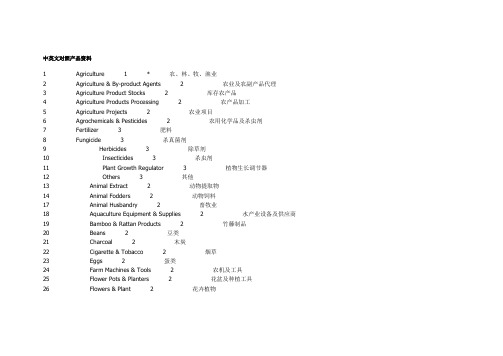
中英文对照产品资料1 Agriculture 1 * 农、林、牧、渔业2 Agriculture & By-product Agents 2 农业及农副产品代理3 Agriculture Product Stocks 2 库存农产品4 Agriculture Products Processing 2 农产品加工5 Agriculture Projects 2 农业项目6 Agrochemicals & Pesticides 2 农用化学品及杀虫剂7 Fertilizer 3 肥料8 Fungicide 3 杀真菌剂9 Herbicides 3 除草剂10 Insecticides 3 杀虫剂11 Plant Growth Regulator 3 植物生长调节器12 Others 3 其他13 Animal Extract 2 动物提取物14 Animal Fodders 2 动物饲料17 Animal Husbandry 2 畜牧业18 Aquaculture Equipment & Supplies 2 水产业设备及供应商19 Bamboo & Rattan Products 2 竹藤制品20 Beans 2 豆类21 Charcoal 2 木炭22 Cigarette & Tobacco 2 烟草23 Eggs 2 蛋类24 Farm Machines & Tools 2 农机及工具25 Flower Pots & Planters 2 花盆及种植工具26 Flowers & Plant 2 花卉植物27 Fodder & Feed Additives 2 化肥及添加剂28 Forest Machinery 2 林业机械29 Frozen & Dried Fruit 2 冷藏干果类30 Fruit 2 水果31 Garden Tools & Equipment 2 园林工具及设备32 Grain 2 谷物33 Irrigation & Watering 2 排灌机械34 Mushroom & Truffle 2 蘑菇菌类35 Nuts & Kernels 2 坚果及干果36 Plant & Animal Oil 2 食用油37 Plant Extract 2 植物提取物38 Plant Seed 2 种子39 Poultry & Livestock 2 家禽及家畜40 Tea 2 茶41 Vegetable 2 蔬菜42 Dehydrated Vegetables 3 脱水蔬菜43 Fresh Preserved Vegetables 3 新鲜蔬菜44 Frozen & Dried Vegetable 3 冷冻蔬菜45 Potato, Sweet Potato & etc. 3 土豆甘薯类46 Salted Vegetables 3 酱腌菜47 Spicy Vegetables 3 辛辣蔬菜48 Others 3 其他49 Others 2 其他50 Food & Beverage 1 * 食品及饮料51 Alcohol 2 酒类52 Aquatic Products 2 水产品53 Baby Food 2 婴儿食品54 Bean Products 2 豆制品55 Beverage Processing Machinery 2 饮料加工设备56 Beverages 2 饮料57 Bread & Biscuit 2 面包糕点58 Canned Food 2 罐头59 Cigarette & Tobacco 2 烟草60 Confectionery 2 糖果61 Cooking Equipment 2 烹饪设备62 Dairy Products 2 乳制品63 Egg Products 2 蛋类64 Fast-Food 2 快餐食品65 Flour 2 面粉66 Food Additives 2 食品添加剂67 Food Agents 2 食品饮料代理68 Food Ingredients 2 食品配料成分69 Chocolate Ingredients 3 巧克力粉70 Cultures, Enzymes & Yeast 3 酵母71 Edible Fats & Oils 3 食用油脂72 Flavors & Flavor Enhancers 3 香料及鲜味剂73 Gums & Stabilizers 3 口香糖及食品稳定剂74 Nutrient Additives 3 营养添加剂75 Spices & Seasonings 3 香味料76 Starch & Derivatives 3 淀粉77 Sugar & Sweeteners 3 甜味剂78 Food Processing 2 食品加工79 Food Processing Machinery 2 食品加工设备80 Food Projects 2 食品项目81 Food Stocks 2 库存食品饮料82 Frozen & Dried Fruit 2 冷冻水果及干果83 Frozen Food 2 冷冻食品84 Health Food 2 健康食品85 Honey Products 2 蜜制品86 Meat & Poultry 2 肉制品87 Noodles 2 面条88 Snacks 2 休闲食品89 Tea 2 茶叶90 Others 2 其他91 Automobile Supplies & Accessories 1 * 汽摩配件92 ATV 2 沙滩车93 Auto Accessories 2 汽车附件94 Auto Electrical System 2 汽车电气系统95 Auto Batteries 3 汽车电池96 Auto Ignition System 3 点火系统97 Auto Lighting System 3 汽车照明系统98 Auto Starter System 3 启动系统99 Generator & Alternator 3 发电机和交流发电机100 Motor 3 发动机101 Relays, Sensors & Switches 3 继电器、传感器、开关102 Speaker & Horn 3 汽车喇叭103 Others 3 其他104 Auto Electronics 2 汽车电子105 Car Audio 3 车载音响106 Car Video 3 车载视频107 Communications 3 车载通讯108 Navigation & GPS 3 GPS导航109 Radar Detector 3 雷达探测器110 Others 3 其他111 Auto Maintenance 2 汽车防护保养112 Auto Parts 2 汽车零部件113 Auto Bearing 3 汽车轴承114 Auto Filter 3 汽车滤清器115 Auto Meter 3 汽车仪表116 Brakes 3 刹车117 Car Glasses & Mirrors 3 汽车玻璃及反光镜118 Clutches & Parts 3 离合器及配件119 Cooling System 3 冷却系统120 Engine Parts & Mounts 3 引擎及支架121 Exhaust System 3 排气系统122 Heating & Air Conditioning System 3 空调系统123 Muffler Assembly 3 消声器总成124 Radiator & Parts 3 水箱及配件125 Security & Safety Products 3 安全保险设备126 Shock Absorbers 3 减震器127 Steering & Transmission Parts 3 转向及传动部件128 Tank & Parts 3 油箱及配件129 Tube Assembly 3 管路总成130 Wheel & Tire Parts 3 车轮及轮胎部件131 Windshield Wipers 3 雨刮器132 Wire Assembly 3 电线总成133 Others 3 其他2001 Auto Electrical Components & Parts 3 汽车电子零部件2002 Auto Exterior Accessories 3 汽车外部零部件2003 Auto Interior Accessories 3 汽车内部零部件2004 Auto Security & Safety Products 3 汽车安全产品2005 Auto Spare Parts & Supplies 3 汽车备件及代理2006 Garage Tools 3 汽车修理工具2007 Motorcycle Accessories & Supplies 3 摩托车配件及供应商2008 Motorcycle parts 3 摩托车零部件134 Auto Production Line Equipment 2 汽车制造设备135 Automobile 2 汽车136 Automobile & Parts Agent 2 汽车及配件代理137 Automobile Stocks 2 库存汽车138 Electric Motorcycles 2 电动机车139 Motorcycle Accessories 2 摩托车配件140 Motorcycle Parts 2 摩托车零部件141 Motorcycles 2 摩托车142 Parking 2 停车场设备143 Second Hand 2 二手车144 Special Transportation Equipment 2 特殊运输设备145 Others 2 其他146 Computer & PC Peripherals 1 * 计算机及外围设备147 Computer 2 电脑2009 Computer Cards 3 计算机卡2010 Computer Cases/Chassis 3 计算机硬件2011 Computer Chips 3 计算机芯片2012 Computer Power Supply 3 计算机电源2013 Computer Server 3 服务器2014 Data Cards & Readers 3 信息卡及读卡器2015 Discs & Drives 3 光盘及磁盘2016 Hub 3 网络集线器2017 Monitors & Displays 3 显示器2018 Motherboards 3 主板2019 Mouse 3 鼠标2020 Multimedia speakers 3 音箱2021 Notebook computers 3 笔记本电脑2022 PCs 3 个人电脑2023 Projector 3 放映机2024 Scanner 3 扫描仪2025 USB flash disk 3 USB闪存148 Computer & Software Agents 2 计算机及软件代理149 Computer Case & PC Case 2 机箱150 Computer Related Projects 2 计算机相关项目151 Computer Consumables 2 计算机消费品152 Hardware Components 2 硬件配件153 I/O Card 2 插卡154 IC Card 2 IC卡155 LCD PC 2 液晶显示屏计算机156 Network Device 2 网络设备157 Network Engineering 2 网络工程158 New Product 2 新产品159 Notebooks & Laptops 2 笔记本电脑160 PDA 2 PDA161 Peripherals 2 电脑用品及外设162 Computer Cables & Connectors 3 电脑接口线163 Digital Photography 3 数码相机164 Drives & Storage Devices 3 磁盘存储设备165 Earphone & Headphone 3 耳机166 Joysticks & Game Controllers 3 游戏控制杆167 Keyboard 3 键盘168 Modems 3 调制解调器169 Monitors & Displays 3 显示器170 Mouse 3 鼠标171 Multimedia Speakers 3 音箱172 PC cameras 3 摄像头173 Printers & Scanners 3 打印机及扫描仪174 Others 3 其他175 Second Hand 2 二手电脑176 Server & WorkStation 2 服务器、工作站177 Software 2 软件178 Software Design 2 软件设计179 UPS & Power Supply 2 UPS电源180 Others 2 其他181 Electronics & Electrical 1 * 电子、电工类产品182 Acoustic Component 2 音响零件183 Batteries & Chargers 2 电池及充电器184 Auto Batteries 3 汽车电池185 Battery Packs 3 电池组186 Battery Testers 3 电池检测器187 Dry Batteries, Disposable Batteries & Primary Batteries 3 干电池、一次性电池及原电池188 Fuel Cells 3 燃料电池189 Lithium Batteries, Nickel Hydride Batteries & Mobile Phone Batteries 3 锂电池、镍电池及手机电池190 Rechargeable Batteries 3 充电电池191 Solar Cells & Solar Panel 3 太阳能电池及电池板192 Storage Batteries & Secondary Batteries 3 蓄电池及可充电电池193 Watch Batteries 3 纽扣电池194 Others 3 其他195 Calculator 2 计算器196 Capacitors 2 电容器197 Chargers 2 充电器198 Circuit Breaker 2 断路器199 Commercial Field 2 商业领域200 Contactor 2 电流接触器201 EL Products 2 电器产品202 Electric Power Tools 2 电动工具203 Electrical Contacts & Contact Materials 2 电触头及电触头材料204 Electrical Outlets & Plugs 2 电器插口及电插头205 Electrical Product Agent 2 电器产品代理206 Electronic & Instrument Enclosures 2 电子乐器及音响207 Electronic Component 2 电子元件208 Electronic Data Systems 2 电子数据系统209 Electronic Instrument 2 电子乐器210 Electronic Signs 2 电子标志211 Electronics Agents 2 电子产品代理212 Electronics Designing & Processing 2 电子设计及加工213 Electronics Projects 2 电子项目214 Electronics Stocks 2 库存电子产品215 Financial Field 2 财经领域216 Fuses 2 保险丝,217 Generators 2 发电机218 High-Low Voltage Electrical Apparatus 2 高低压电子设备219 Insulation 2 绝缘产品220 Keypad & Keyboard 2 键盘221 Laser 2 激光222 LED Backlight 2 LED背景灯223 LED Calendar 2 LED日历224 LED Display 2 LRD显示屏225 Lighting Accessories 2 灯具灯饰226 Ballast & Starter 3 镇流器及触发器227 Lamp Cover & Shade 3 灯罩228 Lighting Transformer 3 照明电子变压器229 Others 3 其他230 Lighting Bulbs & Tubes 2 灯泡及灯管231 Incandescent Bulbs 3 白炽灯泡232 Energy Saving & Fluorescent 3 节能及荧光类233 Bulbs & Tubes 3 普泡/灯管234 HID Bulbs 3 高强度放电灯泡235 Others 3 其他236 Lighting Fixtures 2 照明灯具237 Emergency Lights 3 应急灯238 Flashlights & Torches 3 电筒239 Holiday Lighting 3 节日照明240 Industrial Lighting 3 工业照明242 Residential Lighting 3 居室用灯243 Others 3 其他244 Magnetic Materials 2 磁性材料245 Motors & Engines 2 电机及引擎246 Optical Instrument & Parts 2 光学仪器及配件247 PCB & PCBA 2 印制电路板及印制电路板组248 Power Accessories 2 电源附件249 Power Supplies 2 电源供应250 AC/DC Adapter 3 AC/DC适配器251 Industrial Power Supply 3 工业能源供应252 Inverter & Converter 3 变极器及转炉253 Switching Power Supply 3 开关式电源254 Transformer & Inductor 3 变压器及感应器255 Uninterrupted Power Supply (UPS) 3 UPS256 Voltage Regulator/Stabilizer 3 稳压器257 Others 3 其他258 Professional Audio, Video & Lighting 2 专业音响、摄像及照明259 Radio & TV Equipment 2 广播电视设备260 Rectifiers 2 整流器261 Relays 2 继电器262 Semiconductors 2 半导体263 Sensors 2 传感器264 Speaker 2 扬声器266 Transformers 2 变压器267 Wires, Cables & Cable Assemblies 2 电线电缆268 Audio & Video Cable 3 声频及视频电缆269 Bare Wire 3 光焊丝270 Cable Accessories & Wiring Accessories 3 电线电缆附件271 Cable Harness & Wire Harness 3 线缆装配272 Cable Manufacturing Equipment 3 线缆制造设备273 Communication Cables 3 通信电缆274 Computer Cables & Connectors 3 电脑信号线及连接器275 Connectors & Terminals 3 连接器及终端设备276 Instrumentation Cable 3 控制线缆277 Power Cable 3 电力电缆278 Power Cord 3 电源线279 Specialty Cable Assemblies 3 特殊线缆附件280 Others 3 其他281 Others 2 其他2030 Batteries & Charger 2 电池及充电器2031 AV batteries/packs 3 AV电池及电池组2032 Batteries Charger 3 充电器2033 Dry-cell batteries 3 氢氧电池2034 Lithium batteries/packs 3 锂电池及电池组2035 Notebook computer batteries/packs 3 笔记本电脑电池及电池组2036 Rechargeable batteries/packs 3 充电电池及电池组3220 Telecom batteries/packs 3 通信电源、蓄电池2037 Commercial Lighting 2 商业照明2038 Automobile repairing light 3 汽车修理用灯2039 Ceiling light 3 天花灯2040 Down light 3 筒灯2041 Emergency lighting 3 应急照明2042 Flashlight/Torch 3 手电筒2043 Fluorescent lamp 3 荧光灯具2044 Grille light 3 格栅灯2045 High bay 3 高顶灯2046 Low bay 3 低顶灯2047 Recessed down light 3 嵌灯2048 Stage lighting 3 舞台灯光照明2049 Home Lighting 2 家居灯饰2050 Ceiling mount 3 吸顶灯2051 Chandelier & pendant lamp 3 吊灯2052 Crystal light 3 水晶灯2053 Decorative lighting 3 装饰灯2054 Desk lamp 3 桌灯2055 Juvenile lighting 3 儿童灯2056 Night light 3 夜灯2057 Spot light 3 射灯2058 Table lamp 3 台灯2059 Tiffany lamp 3 蒂凡尼灯/仿蒂凡尼灯2060 Wall lamp 3 壁灯2061 floor lamp 3 落地灯2062 track light 3 导轨灯2063 Light Sources 2 光源2064 Energy-saving lamp/Compact fluorescent lamp/CCFL 3 节能灯/紧凑型荧光灯2065 Halogen bulbs 3 卤素灯泡2066 LED lightsLED 3 LED光源2067 Mosquito-lured lamp 3 诱蚊灯2068 Plant-growth lamp 3 植物生长灯2069 Special light sources 3 特种光源2070 Lighting Parts & Components 2 灯饰零配件2071 Accessory Lights 3 灯饰附件2072 Ballasts 3 镇流器2073 Electric parts 3 电器配件2074 Electrical wire 3 电源线2075 Lamp holder 3 灯头2076 Lampshade 3 灯罩2077 Lighting Hardware fittings 3 灯饰五金配件2078 Lighting components 3 灯饰零件2079 Reflectors & diffusers 3 反光罩/散光罩2080 Socket/Plug 3 插座/插头2081 Switch 3 开关2082 Terminal 3 端子2083 Transformer 3 变压器2084 Outdoor Lighting 2 户外灯2085 Festival lighting 3 节日灯饰2086 Floodlight 3 泛光灯2087 Garden light 3 花园灯/庭院灯2088 Grass lamp 3 草坪灯2089 LED lighting FixtureLED 3 LED应用灯具2090 Pool light 3 水池灯2091 Roadway luminaire/street light 3 路灯/街灯2092 Sensor light 3 感应灯2093 Signal lights 3 信号灯,警示灯2094 Solar lamp 3 阳能灯2095 Three-defend Lamp 3 三防灯(防水、防尘、防雾)2096 Underground lamp 3 埋地灯2097 Work light 3 户外工作灯2098 Audio & Video 2 音频及视频2099 A/V Cables & Connections 3 数字音视频电缆2100 AV Cleaning & Storage 3 AV清洁及存储2101 AV Loader Mechanism 3 AV录制机械2102 Amplifiers & Speakers 3 扩音器及喇叭2103 Antennas 3 天线2104 CATV, Satellite Receiver 3 有线、卫星电视接受器2105 Car AV System 3 汽车音响2106 Combo Cassette Recorder 3 收录组合机2107 Converters, Remotes, Decoders & Switchs 3 转炉、遥控,解码及开关2108 DVD Player 3 DVD2109 Digital Camera 3 数码照相机2110 Gift Radio 3 礼品收音机2111 Headphone, Earphone 3 耳机2112 Home Theater 3 家庭影院2113 Language-learning Tape Recorders 3 语言学习机2114 MP3 Player 3 MP3播放器2115 MP4 Player 3 MP4播放器2116 Micro System/Mini Combo 3 微电子系统及迷你音响2117 Microphones, Loudhailers 3 麦克风及扬声器2118 Portable CD Player 3 CD随身听2119 Portable Cassette Recorder/Player 3 磁带随身听2120 Portable DVD Player 3 便携式DVD2121 Portable VCD Player 3 便携式VCD2122 Professional AV Equipment 3 专业AV设备2123 Radio 3 收音机2124 Recording Media 3 录制设备2125 TV-VCR-DVD Combos 3 TV-VCR-DVD组合播放设备2126 TVs, Display 3 电视、显示器2127 VCD Player 3 VCD播放器2128 VCR 3 录像机2129 Digital Dictionary / Diaries 2 电子词典2130 Digital Dictionary / diaries 3 电子词典2131 Electronics clock 2 电子钟2132 Electronics clock 3 电子钟2133 Games 2 游戏2134 Games Electronics 3 电子游戏类2135 Office Electronics 2 办公电子设备2136 Office Electronics 3 办公电子设备2137 Active Components 2 有源电子电路器件2138 Crystals, Oscillators & Filters 3 晶状体、振荡器及过滤器2139 Digital ICs 3 数码IC2140 Optoelectronic Components 3 光电子元件2141 Transistors, Diodes & Tubes 3 晶体管,二极管等2142 Electromechanical Components 2 机电元件2143 Acoustic Components 3 电声零部件2144 Circuit & Heat Protection Devices 3 电路及热保护设备2145 Magnets & Heads 3 磁铁及磁头2146 Motors & Mechanisms 3 电机及机械2147 Sensors & Transducers 3 传感器2148 Strain Gauge 3 应变仪2149 Switches 3 开关2150 Electronics Manufacturing Materials & Supplies 2 电子制造材料2151 Antistatic Products 3 防静电产品2153 Connectors 3 连接器2154 Plugs, Jacks & Sockets 3 插销、插座2155 Wires, Cables & Assemblies 3 线缆及配件2152 Interconnects & Electricals 2 电子连接部件2156 Passive Components 2 无源元件2157 Capacitors 3 电容器2158 Inductors, Transformers & Coils 3 感应器、变压器及线圈2159 Resistors 3 电阻器2160 Subassemblies & Parts 2 电子元件2161 Magnetrons 3 磁电管2162 Optoelectronic Displays 3 光电显示设备2163 PCBs 3 印刷电路板2164 Parts 3 零部件2165 Power Supplies, Batteries & Accessories 3 电源、电池及配件282 Fashion 1 * 服装时尚类产品283 Apparel & Fashion Agents 2 服饰风尚产品代理284 Apparel Designing & Processing 2 服装设计加工285 Apparel Projects 2 服装项目286 Apparel Stocks 2 库存服饰287 Athletic Wear 2 运动服装288 Bathrobe 2 浴衣290 Costume & Ceremony 2 礼服291 Down Garment 2 羽绒服292 Ethnic Garment 2 民族服装321 Footwear 2 鞋类322 Women's Boots 3 女装靴323 Kids' Shoes 3 童鞋324 Men's Dress Shoes 3 男士皮鞋325 Safety Shoes 3 防护鞋类326 Women's Sandals & slippers 3 女装凉鞋/拖鞋/沙滩鞋327 Shoes Parts, Materials & Accessories 3 制鞋材料及附件328 Men's Sandals & slippers 3 男装凉鞋/拖鞋/沙滩鞋329 Special Purpose Shoes 3 特殊用途鞋类330 Sports shoes 3 运动鞋331 Women's Casual Shoes 3 女士休闲鞋332 Others 3 其他3212 Men's Boots 3 男装靴3213 Men's Casual Shoes 3 男士休闲鞋333 Fur Garment 2 皮衣334 Trimmings, Accessories & Supplies 2 装饰,点缀品及附属品335 Zippers, Buttons & Closures/Fittings 3 拉链,纽扣及带扣/配件336 Hooks & Loops 3 挂钩及圈结337 Interlinings & Linings 3 夹层及内衬338 Labels & Tags 3 牌子及标签339 Laces & Tassel Cords 3 蕾丝及流苏341 Others 3 其他2202 Garment Parts & Accessories 3 成衣配件及饰品2203 Trimming Materials & Supplies 3 点缀材料342 Gloves & Mittens 2 手套343 Infant Garment 2 婴儿服饰346 Leather Garment 2 皮状347 Leisure Wear 2 休闲服饰348 Mannequins & Forms 2 服装模特349 Outerwear 2 外套351 Related Machine 2 服装相关机械352 Sewing Machinery 2 缝纫机354 Silk Garment 2 丝绸服饰356 Socks & Stockings 2 袜子357 Speciality 2 特殊服装360 Swimwear & Beachwear 2 泳衣及沙滩装362 Underwear & Nightwear 2 内衣及睡衣363 Bras & Lingerie 3 胸罩及女士内衣364 Briefs, Panties, Thongs & Boxers 3 短裤,童裤及腰带365 Camisoles, Spencers & Vests 3 妇女短袖衬衣366 Long Johns 3 长内衣裤367 Pajamas, Sleepwear & Loungewear 3 睡衣368 Shapers 3 塑身衣369 Underwear Accessories 3 内衣附件370 Underwear Set 3 内衣裤装饰371 Others 3 其他2204 Nightwear & sleepwear 3 睡衣/家居服373 Used Clothes 2 旧装374 Winter Clothes 2 冬衣375 Others 2 其他376 Clocks 2 钟表377 Antique Clocks 3 仿古钟378 Clock Agents 3 钟类代理379 Clock Parts & Accessories 3 钟表零配件380 Desk & Table Clocks 3 桌式、台式钟381 Digital & Analog-Digital Clocks 3 数码钟及模拟数字钟382 Floor Clocks 3 落地钟383 Hourglasses 3 沙漏384 Mechanical Clocks 3 机械钟385 Specialty Clocks 3 特殊钟386 Wall Clocks 3 壁钟387 Others 3 其他388 Eyewear 2 眼镜389 Contact Lenses 3 隐形眼镜390 Eyeglass Frames 3 眼镜框391 Eyeglass Lenses 3 镜片392 Eyeglass Parts 3 眼镜配件393 Contact Lens Care Products 3 镜片保养产品394 Contact Lens Cases 3 镜片盒395 Eyeglass Care Products 3 眼镜保养品396 Eyeglass Cases & Bags 3 眼镜盒及包397 Eyewear Agents 3 眼镜代理398 Eyewear Displays 3 眼镜展示设备399 Reading Glasses 3 读书镜400 Sports Eyewear 3 运动眼镜401 Sunglasses 3 太阳镜402 Others 3 其他403 Jewelry 2 珠宝404 Bangles & Bracelets 3 手镯、脚链405 Body Jewelry 3 首饰406 Brooches 3 胸针407 Cuff Links 3 纽扣408 Earrings 3 耳环409 Jewelry Set 3 首饰附件410 Magnetic Jewelry 3 磁性首饰411 Necklaces 3 项链412 Rings 3 戒指413 Tie Clips, Tie Bars & Tie Pins 3 领带夹414 Diamond Jewelry 3 钻石类415 Gemstone Jewelry 3 宝石类416 Gold Jewelry 3 黄金饰品417 Jade Jewelry 3 玉饰418 Pearl Jewelry 3 珍珠饰品419 Platinum Jewelry 3 铂金首饰420 Silver & Sterling Silver Jewelry 3 银饰421 Pearls 3 珍珠422 Precious Stones 3 宝石423 Semi-Precious Stones 3 准宝石424 Synthetic Stones 3 人造宝石425 Others 3 其他426 Watches 2 手表427 Jewellery Cases/Boxes 3 珠宝箱/盒428 Jewelry Agents 3 珠宝代理429 Jewelry Display & Packaging 3 珠宝展示及包装430 Jewelry Findings & Components 3 珠宝附件及配件431 Jewelry Making Tools & Equipment 3 首饰制作工具及设备432 Analog-Digital Watches 3 电子表433 Antique Watches 3 仿古表434 Digital Watches 3 数码表435 Mechanical Watches 3 机械表436 Pocket Watches 3 怀表437 Quartz Analog Watches 3 石英表438 Specialty Watches 3 特殊表类439 Sports Watches 3 运动表440 Watch Agents 3 表类代理441 Watch Bands, Straps & Bracelets 3 表带442 Watch Batteries 3 表用电池443 Watch Boxes & Cases 3 手表盒444 Watch Movements 3 表芯445 Others 3 其他2174 Fashion/Ready-to-Wear Garments 2 成衣2175 Blouses & Women's top女式上衣 3 女式上衣2176 Children's wear & Infants' wear 3 童装&婴儿装2177 Full dress/Wedding Wear & Accessories 3 礼服/婚宴服装/配饰2178 Jeans wear 3 牛仔装2179 Men's Shirts 3 衬衫2180 Polo shirts/T-shirtsPolo 3 衬衫/T 恤衫2181 Rainwear 3 雨衣2182 Sporting Wear 3 运动服2183 Suits 3 西装2184 Trousers & shorts 3 裤子2185 Windbreakers 3 风衣2186 Women's dresses & Skirts 3 裙子2187 Work wear 3 工作服2188 fashion jackets/winter jackets 3 流行夹克/冬季夹克2189 pullovers & sweaters 3 套衫/毛线衫2190 winter coats & overcoats 3 大衣/外套2191 Undergarments 2 内衣2192 Children's underwear 3 儿童内衣2193 Men's underwear 3 男式内衣2194 Women's underwear 3 女式内衣2195 Fashion Accessories 2 时尚类附件294 Belts & Accessories 3 腰带及附件295 Bangles & Bracelets 3 手镯、脚链296 Body Jewelry 3 首饰297 Brooches 3 胸针298 Cuff Links 3 纽扣299 Earrings 3 耳环300 Jewelry Set 3 首饰附件301 Magnetic Jewelry 3 磁性首饰302 Necklaces 3 项链303 Rings 3 戒指304 Tie Clips, Tie Bars & Tie Pins 3 领带夹305 Diamond Jewelry 3 钻石类306 Gemstone Jewelry 3 宝石类307 Gold Jewelry 3 黄金饰品308 Jade Jewelry 3 玉饰309 Pearl Jewelry 3 珍珠饰品310 Platinum Jewelry 3 铂金首饰311 Silver & Sterling Silver Jewelry 3 银饰312 Hair Ornaments 3 发饰313 Hats & Caps 3 帽子314 Handbags & Totebags 3 手包及手提袋316 Polyester Neckties 3 聚酯领结317 Silk Neckties 3 丝制领结318 Scarves & Shawls 3 领带、披肩及围巾319 Sunglasses 3 太阳镜320 Others 3 其他2196 Eyewear & Optical Supplies 3 眼镜2197 Handkerchiefs & brooch 3 手帕/胸针2198 Handwear 3 手饰2199 Headwear 3 头饰2200 Hosiery 3 袜子2201 Neckwear 3 颈饰446 Furniture & Furnishing 1 * 家具及家装产品447 Antique & Reproduction Furniture 2 仿古家具448 Bamboo, Rattan & Wicker Furniture 2 竹编、藤编家具449 Commercial Furniture 2 商业家具450 Bar Furniture 3 酒吧家具451 Cinema, Theater & Auditorium Furniture 3 影剧院家具452 Hotel Furniture 3 酒店家具453 Computer Desks 3 电脑桌454 Conference Room Furniture 3 会议室家具455 Filing & Storage Cabinets 3 储物柜456 Lobby/Reception Furniture 3 前台家具457 Magazine Racks 3 杂志栏458 Office & Industrial Furniture 3 办公及工业家具461 Restaurant Furniture 3 饭店家具462 Others 3 其他2205 Commercial/Institutional Furniture 3 商业及制式家具463 Folding Furniture 2 折叠家具464 Furniture Agents 2 家具代理465 Furniture Hardware 2 家具硬件466 Door Stops & Door Closers 3 门阻器及闭门器467 Furniture Bolts 3 家具用螺丝468 Furniture Caster Wheels 3 "脚轮"469 Furniture Handles & Knobs 3 家具手柄及捏手470 Furniture Hinges 3 合叶471 Furniture Locks 3 锁472 Slides 3 滑轮473 Others 3 其他474 Furniture Making Tools & Machinery 2 家具制造工具及设备475 Furniture Parts & Accessories 2 家具零部件476 Glass Furniture 2 玻璃家具477 Home Decor 2 家居装饰478 Antique Clocks 3 仿古钟479 Artificial Plants & Flowers 3 装饰花木480 Candles & Holders 3 蜡烛及烛台481 Carpet 3 地毯482 Curtain 3 窗、门帘483 Cushion 3 衬垫484 Floor Clocks 3 落地钟485 Incense & Incensory 3 熏香486 Paintings & Calligraphies 3 油画及书法487 Photo & Picture Frame 3 相片及相框488 Rug & Mat 3 地毯, 垫子489 Screens & Room Dividers 3 屏风490 Table Cloth 3 桌布491 Bamboo & Wooden Vases 3 竹、木制花瓶492 Ceramic & Porcelain Vases 3 陶瓷花瓶493 Glass & Crystal Vases 3 玻璃水晶花瓶494 Metal Vases 3 金属花瓶495 Wall Clocks 3 壁钟496 Awning & Canopy 3 遮阳篷497 Blind, Shade & Shutter 3 百叶窗498 Window Hardware & Accessory 3 窗户零部件499 Other 3 其他2206 Home Décor 3 家居装饰500 Home Furniture 2 家庭家具501 Bath Mirror 3 卫生间镜502 Bathroom Cabinets 3 浴室用品箱503 Towel Racks, Bath Racks & Paper Holders 3 毛巾架、纸筒504 Air Beds & Mattresses 3 气床及床垫505 Armoires & Wardrobes 3 衣厨柜506 Bedroom Furniture 3 卧室家具508 Dressers 3 梳妆台509 Nightstands 3 床头几510 Buffets & Hutches 3 餐具柜511 Dining Furniture 3 餐厅家具514 Kitchen Furniture 3 厨房家具515 Bookcases & Bookshelves 3 书柜、书架516 Cabinets & Chests 3 柜子、箱子517 CD Racks 3 CD架518 Chairs & Recliners 3 椅子及躺椅519 Chaise Lounge 3 睡椅520 Coat Racks 3 挂衣架521 Coffee, End & Tea Table 3 茶几522 Shoe Racks 3 鞋架523 Sofas & Sofa Beds 3 沙发及沙发床524 Stool & Ottoman 3 凳子及墩子525 TV Stands 3 电视柜526 Nursery Furniture & Decor 3 医用家具及装饰527 Others 3 其他2207 Living room Furniture 3 起居室家具2299 Baby & Children's Furniture 3 儿童家具2300 Bathroom, Bar & Kitchen Furniture 3 浴室、酒吧及厨房家具528 Inflatable Furniture 2 膨胀家具529 Institutional Furniture 2 组合家具530 Hospital Furniture 3 医院家具531 Laboratory Furniture 3 实验室家具532 Library Furniture 3 图书馆家具533 School Furniture 3 学校家具534 Others 3 其他535 Metal Furniture 2 金属家具536 Outdoor Furniture 2 户外家具537 Beach & Camping Furniture 3 野营家具538 Garden & Patio Sets 3 花园家具539 Garden Gazebo & Pavilion 3 遮阳篷540 Garden Tables/Picnic Tables 3 野餐桌541 Hammocks 3 吊床542 Mailboxes 3 信箱543 Outdoor Umbrellas & Bases 3 户外雨伞544 Patio Benches/Chairs 3 花园椅凳545 Patio Swings 3 摇椅546 Others 3 其他2302 Garden/Outdoor Furniture 3 花园/户外家具547 Plastic Furniture 2 塑料家具548 Wooden & Panel Furniture 2 木制家具549 Others 2 其他550 Gifts & Crafts 1 * 礼品及工艺品551 Antique Imitation Crafts 2 以传统工艺仿造的古董赝品552 Antiques & Collectibles 2 古董收藏品553 Artificial Crafts 2 非原产地的手工艺品554 Arts Designing 2 艺术设计品555 Bamboo & Wooden Crafts 2 以竹子或木头为原材料的工艺品556 Basketry 2 诸如蓝筐之类的手工编制的篓编织品557 Candles & Holders 2 蜡烛;有烛台的蜡烛558 Carving Crafts 2 主要使用雕刻工艺制作的工艺品559 Clay Figurine 2 小雕像560 Crafts Gifts 2 用做礼品的手工艺品561 Crystal 2 主要原材料为水晶的手工艺品562 Embroidery & Crafts Textile 2 刺绣类的手工艺纺织品563 Folk Crafts 2 传统的民间工艺品564 Gifts & Crafts Agents 2 礼品和手工艺品代理商565 Gifts & Crafts Stocks 2 礼品和库存手工艺品566 Glassware 2 玻璃器具类567 Holiday Gift & Decoration 2 特定假日里使用的礼物或装饰品568 Holiday Lighting 2 特定假日里使用的照明用品569 Hourglasses 2 沙漏570 Incense & Incensory 2 熏香或香炉571 Jade Crafts 2 原产地为日本的手工艺品572 Key Chain 2 用于系挂钥匙的钥匙链573 Metal Crafts 2 主要制作材料为金属的手工艺品574 Natural Crafts 2 更多地保持制作原料的自然原貌的手工艺品575 Paintings & Calligraphies 2 作为礼物的油画或书法作品576 Paints Crafts 2 用做礼物的油画577 Paper Crafts 2 以纸张为主要原料的手工艺品578 Photo & Picture Frame 2 用于放置相片或图画的框架579 Photo Album 2 用于放置照片的相册580 Plastic Crafts 2 以塑料为主要原材料的手工艺品581 Pottery & Enamel 2 陶器、珐琅或瓷釉582 Promotion Gifts 2 用于各种比赛中的奖品583 Pyrography 2 用电烙铁绘制的烙画584 Religious Crafts 2 用于宗教用途的手工艺品585 Resinic Crafts 2 主要原材料是树脂的手工艺品586 Sculptures 2 雕刻品或雕塑品587 Stone Carving & Sculpture 2 以石头为主要原材料的雕刻和手工艺品588 Bamboo & Wooden Vases 2 以竹子或木头为主要原料的管状手工艺品589 Ceramic & Porcelain Vases 2 以陶瓷为主要原料的管状手工艺品590 Glass & Crystal Vases 2 以玻璃或水晶为主要原料的管状手工艺品591 Metal Vases 2 以金属为主要原料的管状手工艺品592 Others 2 其他593 Health & Beauty 1 * 健康及美容产品594 Beauty Products Agents 2 美容产品代理商595 Bio-technology Products 2 生物科技产品596 Disabilities 2 辅助产品597 Enzyme (Ferment) Preparations 2 酶、酵产品598 Health Product Agents 2 健康产品代理599 Health Projects 2 健康项目600 Home Healthcare Equipment 2 主要针对家庭使用而设计的健康设备601 Hospital Furniture 2 主要针对医院使用而设计的健康设备602 Massager 2 按摩产品或设备603 Medical Equipment 2 用于内科使用的医疗设备604 Medical Implements 2 医疗器械工作中使用的工具或器械605 Medical Testing & Laboratory Apparatus 3 医疗测试或医疗实验室使用的器械606 Self-Examination Monitors & Instruments 3 用于自我检查使用的监视器或相关设备607 Surgical Instruments 3 外科用医疗设备608 Traditional Therapies 3 传统的医疗设备609 Others 3 其他610 Medical Supplies 2 医疗设备供应商611 Medicine & Health Products 2 医药保健品612 Drugs & Medications 3 药片、药物或药剂613 Health Care Products 3 保健品614 Health Food 3 保健食品615 Herb Medicine 3 经过加工的中草药616 Herbs & Natural Remedies 3 未经加工的天然草药617 Personal Care 2 个人护理用品618 Bath 3 浴室、浴盆、浴缸619 Beauty Equipment 3 美容保健设备620 Breast Care 3 胸部护理设备621 Contact Lens Care Products 3 用于护理隐形眼镜的产品622 Contact Lens Cases 3 隐形眼镜盒623 Contact Lenses 3 隐形眼镜624 Cosmetic Accessories 3 化妆品附件625 Cosmetics 3 化妆品626 Dental Hygiene 3 口腔卫生护理产品627 Electric Shavers 3 电动剔须刀628 Flavour & Fragrance 3 香水或体味调节品629 Hair 3 头发护理产品:包括梳子、电吹风、头发染色剂等630 Nail Care 3 指甲刀、指甲剪631 Razors & Shaving Products 3 用于刮胡子的剃刀等产品632 Reading Glasses 3 放大镜633 Skin Care 3 皮肤护理产品,诸如护手霜、护理油、面膜等634 Soap 3 香皂635 Weight Loss 3 减肥用品636 Others 3 其他2208 Personal Care 3 个人护理用品637 Pharmaceutic Machinery 2 药品调制器械638 Pharmaceutical Chemicals 2 药品药物产品或药物制配639 Pharmacy Stocks 2 配药用原材料640 Sex Products 2 性用品641 Therapies 2 治疗方法642 Veterinary Medicine 2 用于治疗动物的兽医药品643 Weight Loss 2 减肥产品644 Others 2 其他645 Home Products 1 * 家居产品647 HVAC 2 空调2210 Household Air-conditioner 3 家用空调2211 Industrial/Commercial Air-conditioner 3 工业商业用空调2212 Health Scale 3 康体秤648 Audio & Video Equipment 2 音频或视频设备649 Amplifier 3 放大器尤指利用晶体管或电子管使电子信号放大的仪器。
SN74ALS169BDRG4,SN74ALS169BNSRE4,SN74ALS169BNSRG4,SN74ALS169BN,SN74ALS169BNE4, 规格书,Datasheet 资料
Addendum-Page 1PACKAGING INFORMATIONOrderable DeviceStatus(1)Package Type PackageDrawingPins Package QtyEco Plan(2)Lead/Ball Finish MSL Peak Temp (3)Samples (Requires Login)83025012A ACTIVE LCCC FK 201TBD Call TI Call TI 8302501EA ACTIVE CDIP J 161TBD Call TI Call TI 8302501FA OBSOLETE CFP W 16TBD Call TI Call TIJM38510/38003B2A ACTIVE LCCC FK 201TBD POST-PLATE N / A for Pkg Type JM38510/38003BEA ACTIVE CDIP J 161TBD A42N / A for Pkg Type M38510/38003B2A ACTIVE LCCC FK 201TBD POST-PLATE N / A for Pkg TypeM38510/38003BEA ACTIVE CDIP J 161TBD A42N / A for Pkg Type SN54ALS169BJ ACTIVE CDIP J 161TBD A42N / A for Pkg Type SN54AS169AJ OBSOLETE CDIP J 16TBDCall TICall TISN74ALS169BD ACTIVE SOIC D 1640Green (RoHS & no Sb/Br)CU NIPDAU Level-1-260C-UNLIM SN74ALS169BDE4ACTIVE SOIC D 1640Green (RoHS & no Sb/Br)CU NIPDAU Level-1-260C-UNLIM SN74ALS169BDG4ACTIVE SOIC D 1640Green (RoHS & no Sb/Br)CU NIPDAU Level-1-260C-UNLIM SN74ALS169BDR ACTIVE SOIC D 162500Green (RoHS & no Sb/Br)CU NIPDAU Level-1-260C-UNLIM SN74ALS169BDRE4ACTIVE SOIC D 162500Green (RoHS & no Sb/Br)CU NIPDAU Level-1-260C-UNLIM SN74ALS169BDRG4ACTIVE SOIC D 162500Green (RoHS & no Sb/Br)CU NIPDAU Level-1-260C-UNLIM SN74ALS169BN ACTIVE PDIP N 1625Pb-Free (RoHS)CU NIPDAU N / A for Pkg Type SN74ALS169BNE4ACTIVE PDIP N 1625Pb-Free (RoHS)CU NIPDAU N / A for Pkg Type SN74ALS169BNSR ACTIVE SO NS 162000Green (RoHS & no Sb/Br)CU NIPDAU Level-1-260C-UNLIM SN74ALS169BNSRE4ACTIVE SO NS 162000Green (RoHS & no Sb/Br)CU NIPDAU Level-1-260C-UNLIM SN74ALS169BNSRG4ACTIVE SO NS 162000Green (RoHS & no Sb/Br)CU NIPDAU Level-1-260C-UNLIM SN74AS169AN ACTIVE PDIP N 1625Pb-Free (RoHS)CU NIPDAU N / A for Pkg Type SN74AS169ANE4ACTIVE PDIP N 1625Pb-Free (RoHS)CU NIPDAU N / A for Pkg Type SNJ54ALS169BFKACTIVELCCCFK201TBDPOST-PLATE N / A for Pkg Type芯天下--/Addendum-Page 2Orderable Device Status(1)Package Type PackageDrawingPins Package QtyEco Plan(2)Lead/Ball FinishMSL Peak Temp (3)Samples (Requires Login)SNJ54ALS169BJ ACTIVE CDIP J 161TBD A42N / A for Pkg Type SNJ54AS169AFK OBSOLETE LCCC FK 20TBD Call TI Call TI SNJ54AS169AJOBSOLETECDIPJ16TBDCall TICall TI(1)The marketing status values are defined as follows:ACTIVE: Product device recommended for new designs.LIFEBUY: TI has announced that the device will be discontinued, and a lifetime-buy period is in effect.NRND: Not recommended for new designs. Device is in production to support existing customers, but TI does not recommend using this part in a new design.PREVIEW: Device has been announced but is not in production. Samples may or may not be available.OBSOLETE: TI has discontinued the production of the device.(2)Eco Plan - The planned eco-friendly classification: Pb-Free (RoHS), Pb-Free (RoHS Exempt), or Green (RoHS & no Sb/Br) - please check /productcontent for the latest availability information and additional product content details.TBD: The Pb-Free/Green conversion plan has not been defined.Pb-Free (RoHS): TI's terms "Lead-Free" or "Pb-Free" mean semiconductor products that are compatible with the current RoHS requirements for all 6 substances, including the requirement that lead not exceed 0.1% by weight in homogeneous materials. Where designed to be soldered at high temperatures, TI Pb-Free products are suitable for use in specified lead-free processes.Pb-Free (RoHS Exempt): This component has a RoHS exemption for either 1) lead-based flip-chip solder bumps used between the die and package, or 2) lead-based die adhesive used between the die and leadframe. The component is otherwise considered Pb-Free (RoHS compatible) as defined above.Green (RoHS & no Sb/Br): TI defines "Green" to mean Pb-Free (RoHS compatible), and free of Bromine (Br) and Antimony (Sb) based flame retardants (Br or Sb do not exceed 0.1% by weight in homogeneous material)(3)MSL, Peak Temp. -- The Moisture Sensitivity Level rating according to the JEDEC industry standard classifications, and peak solder temperature.Important Information and Disclaimer:The information provided on this page represents TI's knowledge and belief as of the date that it is provided. TI bases its knowledge and belief on information provided by third parties, and makes no representation or warranty as to the accuracy of such information. Efforts are underway to better integrate information from third parties. TI has taken and continues to take reasonable steps to provide representative and accurate information but may not have conducted destructive testing or chemical analysis on incoming materials and chemicals.TI and TI suppliers consider certain information to be proprietary, and thus CAS numbers and other limited information may not be available for release.In no event shall TI's liability arising out of such information exceed the total purchase price of the TI part(s) at issue in this document sold by TI to Customer on an annual basis.OTHER QUALIFIED VERSIONS OF SN54ALS169B, SN54AS169A, SN74ALS169B, SN74AS169A :•Catalog: SN74ALS169B , SN74AS169A •Military: SN54ALS169B , SN54AS169ANOTE: Qualified Version Definitions:芯天下--/PACKAGE OPTION ADDENDUM25-Jan-2012Addendum-Page 3•Catalog - TI's standard catalog product•Military - QML certified for Military and Defense Applications芯天下--/TAPE AND REELINFORMATION*Alldimensions are nominalDevicePackage Type Package Drawing Pins SPQReel Diameter (mm)Reel Width W1(mm)A0(mm)B0(mm)K0(mm)P1(mm)W (mm)Pin1Quadrant SN74ALS169BDR SOIC D 162500330.016.4 6.510.3 2.18.016.0Q1SN74ALS169BNSRSONS162000330.016.48.210.52.512.016.0Q114-Jul-2012*Alldimensions are nominalDevice Package TypePackage DrawingPins SPQ Length (mm)Width (mm)Height (mm)SN74ALS169BDR SOIC D 162500333.2345.928.6SN74ALS169BNSRSONS162000367.0367.038.014-Jul-2012IMPORTANT NOTICETexas Instruments Incorporated and its subsidiaries(TI)reserve the right to make corrections,enhancements,improvements and other changes to its semiconductor products and services per JESD46C and to discontinue any product or service per JESD48B.Buyers should obtain the latest relevant information before placing orders and should verify that such information is current and complete.All semiconductor products(also referred to herein as“components”)are sold subject to TI’s terms and conditions of sale supplied at the time of order acknowledgment.TI warrants performance of its components to the specifications applicable at the time of sale,in accordance with the warranty in TI’s terms and conditions of sale of semiconductor products.Testing and other quality control techniques are used to the extent TI deems necessary to support this warranty.Except where mandated by applicable law,testing of all parameters of each component is not necessarily performed.TI assumes no liability for applications assistance or the design of Buyers’products.Buyers are responsible for their products and applications using TI components.To minimize the risks associated with Buyers’products and applications,Buyers should provide adequate design and operating safeguards.TI does not warrant or represent that any license,either express or implied,is granted under any patent right,copyright,mask work right,or other intellectual property right relating to any combination,machine,or process in which TI components or services are rmation published by TI regarding third-party products or services does not constitute a license to use such products or services or a warranty or endorsement e of such information may require a license from a third party under the patents or other intellectual property of the third party,or a license from TI under the patents or other intellectual property of TI.Reproduction of significant portions of TI information in TI data books or data sheets is permissible only if reproduction is without alteration and is accompanied by all associated warranties,conditions,limitations,and notices.TI is not responsible or liable for such altered rmation of third parties may be subject to additional restrictions.Resale of TI components or services with statements different from or beyond the parameters stated by TI for that component or service voids all express and any implied warranties for the associated TI component or service and is an unfair and deceptive business practice. TI is not responsible or liable for any such statements.Buyer acknowledges and agrees that it is solely responsible for compliance with all legal,regulatory and safety-related requirements concerning its products,and any use of TI components in its applications,notwithstanding any applications-related information or support that may be provided by TI.Buyer represents and agrees that it has all the necessary expertise to create and implement safeguards which anticipate dangerous consequences of failures,monitor failures and their consequences,lessen the likelihood of failures that might cause harm and take appropriate remedial actions.Buyer will fully indemnify TI and its representatives against any damages arising out of the use of any TI components in safety-critical applications.In some cases,TI components may be promoted specifically to facilitate safety-related applications.With such components,TI’s goal is to help enable customers to design and create their own end-product solutions that meet applicable functional safety standards and requirements.Nonetheless,such components are subject to these terms.No TI components are authorized for use in FDA Class III(or similar life-critical medical equipment)unless authorized officers of the parties have executed a special agreement specifically governing such use.Only those TI components which TI has specifically designated as military grade or“enhanced plastic”are designed and intended for use in military/aerospace applications or environments.Buyer acknowledges and agrees that any military or aerospace use of TI components which have not been so designated is solely at the Buyer's risk,and that Buyer is solely responsible for compliance with all legal and regulatory requirements in connection with such use.TI has specifically designated certain components which meet ISO/TS16949requirements,mainly for automotive ponents which have not been so designated are neither designed nor intended for automotive use;and TI will not be responsible for any failure of such components to meet such requirements.Products ApplicationsAudio /audio Automotive and Transportation /automotiveAmplifiers Communications and Telecom /communicationsData Converters Computers and Peripherals /computersDLP®Products Consumer Electronics /consumer-appsDSP Energy and Lighting /energyClocks and Timers /clocks Industrial /industrialInterface Medical /medicalLogic Security /securityPower Mgmt Space,Avionics and Defense /space-avionics-defense Microcontrollers Video and Imaging /videoRFID OMAP Mobile Processors /omap TI E2E Community Wireless Connectivity /wirelessconnectivityMailing Address:Texas Instruments,Post Office Box655303,Dallas,Texas75265Copyright©2012,Texas Instruments Incorporated芯天下--/。
multisim元件中英对照
Multisim元件库名称中英文对照表1.Source库:包括电源、信号电压源、信号电流源、可控电压源、可控电流源、函数控制器件6个类。
2。
BASIC库:包含基础元件,如电阻、电容、电感、二极管、三极管、开关等;3。
Diodes:二极管库,包含普通二极管、齐纳二极管、二极管桥、变容二极管、PIN二极管、发光二极管等。
4。
Transisitor库:三极管库,包含NPN、PNP、达林顿管、IGBT、MOS管、场效应管、可控硅等;5。
Analog库:模拟器件库,包括运放、滤波器、比较器、模拟开关等模拟器件6。
TTL库:包含TTL型数字电路如7400 7404等门BJT电路。
7。
COMS库:COMS型数字电路如74HC00 74HC04等MOS管电路。
8。
MCU Model: MCU模型,Multisim的单片机模型比较少,只有8051 PIC16的少数模型和一些ROM RAM等9。
Advance Periphearls库:外围器件库,包含键盘、LCD、和一个显示终端的模型。
10。
MIXC Digital:混合数字电路库,包含DSP、CPLD、FPGA、PLD、单片机-微控制器、存储器件、一些接口电路等数字器件。
11。
Mixed:混合库,包含定时器、AC/DA转换芯片、模拟开关、震荡器等;12。
Indicators:指示器库,包含电压表、电流表、探针、蜂鸣器、灯、数码管等等显示器件。
13。
Power:电源库,包含保险丝、稳压器、电压抑制、隔离电源等14。
Misc:混合库,包含晶振、电子管、滤波器、MOS驱动、和其他一些器件等15。
RF:RF库,包含一些RF器件,如高频电容电感、高频三极管等16。
Elector Mechinical:电子机械器件库,包含传感开关、机械开关、继电器、电机等。
2.1. 电阻固定电阻:RES半导体电阻:RESSEMT电位计;POT变电阻;RVAR可调电阻;res12. 电容定值无极性电容;CAP定值有极性电容;CAP半导体电容:CAPSEMI可调电容:CAPVAR3. 电感:INDUCTOR4. 二极管:DIODE.LIB发光二极管:LED5. 三极管:NPN16. 结型场效应管:JFET.lib7. MOS场效应管8. MES场效应管9. 继电器:PELAY. LIB10. 灯泡:LAMP11. 运放:OPAMP12. 数码管:DPY_7-SEG_DP (MISCELLANEOUS DEVICES.LIB)13. 开关;sw_pb原理图常用库文件:Miscellaneous Devices.ddbDallas Microprocessor.ddbIntel Databooks.ddbProtel DOS Schematic Libraries.ddbPCB元件常用库:Advpcb.ddbGeneral IC.ddbMiscellaneous.ddb部分分立元件库元件名称及中英对照AND 与门ANTENNA 天线BATTERY 直流电源BELL 铃,钟BVC 同轴电缆接插件BRIDEG 1 整流桥(二极管)BRIDEG 2 整流桥(集成块)BUFFER 缓冲器BUZZER 蜂鸣器CAP 电容CAPACITOR 电容CAPACITOR POL 有极性电容CAPVAR 可调电容CIRCUIT BREAKER 熔断丝COAX 同轴电缆CON 插口CRYSTAL 晶体整荡器DB 并行插口DIODE 二极管DIODE SCHOTTKY 稳压二极管DIODE VARACTOR 变容二极管DPY_3-SEG 3段LEDDPY_7-SEG 7段LEDDPY_7-SEG_DP 7段LED(带小数点)ELECTRO 电解电容FUSE 熔断器INDUCTOR 电感INDUCTOR IRON 带铁芯电感INDUCTOR3 可调电感JFET N N沟道场效应管JFET P P沟道场效应管LAMP 灯泡LAMP NEDN 起辉器LED 发光二极管METER 仪表MICROPHONE 麦克风MOSFET MOS管MOTOR AC 交流电机MOTOR SERVO 伺服电机NAND 与非门NOR 或非门NOT 非门NPN NPN三极管NPN-PHOTO 感光三极管OPAMP 运放OR 或门PHOTO 感光二极管PNP 三极管NPN DAR NPN三极管PNP DAR PNP三极管POT 滑线变阻器PELAY-DPDT 双刀双掷继电器RES1.2 电阻RES3.4 可变电阻RESISTOR BRIDGE ? 桥式电阻RESPACK ? 电阻SCR 晶闸管PLUG ? 插头PLUG AC FEMALE 三相交流插头SOCKET ? 插座SOURCE CURRENT 电流源SOURCE VOLTAGE 电压源SPEAKER 扬声器SW ? 开关SW-DPDY ? 双刀双掷开关SW-SPST ? 单刀单掷开关SW-PB 按钮THERMISTOR 电热调节器TRANS1 变压器TRANS2 可调变压器TRIAC ? 三端双向可控硅TRIODE ? 三极真空管VARISTOR 变阻器ZENER ? 齐纳二极管DPY_7-SEG_DP 数码管SW-PB 开关其他元件库Protel Dos Schematic 4000 Cmos .Lib (40.系列CMOS管集成块元件库)4013 D 触发器4027 JK 触发器Protel Dos Schematic Analog Digital.Lib(模拟数字式集成块元件库)AD系列DAC系列HD系列MC系列Protel Dos Schematic Comparator.Lib(比较放大器元件库)Protel Dos Shcematic Intel.Lib(INTEL公司生产的80系列CPU集成块元件库)Protel Dos Schematic Linear.lib(线性元件库)例555Protel Dos Schemattic Memory Devices.Lib(内存存储器元件库)Protel Dos Schematic SYnertek.Lib(SY系列集成块元件库)Protes Dos Schematic Motorlla.Lib(摩托罗拉公司生产的元件库)Protes Dos Schematic NEC.lib(NEC公司生产的集成块元件库)Protes Dos Schematic Operationel Amplifers.lib(运算放大器元件库)Protes Dos Schematic TTL.Lib(晶体管集成块元件库74系列)Protel Dos Schematic Voltage Regulator.lib(电压调整集成块元件库)Protes Dos Schematic Zilog.Lib(齐格格公司生产的Z80系列CPU集成块元件库)原理图常用库文件:Miscellaneous Devices.ddbDallas Microprocessor.ddbIntel Databooks.ddbProtel DOS Schematic Libraries.ddbPCB元件常用库:Advpcb.ddbGeneral IC.ddbMiscellaneous.ddb部分分立元件库元件名称及中英对照AND 与门ANTENNA 天线BATTERY 直流电源BELL 铃,钟BVC 同轴电缆接插件BRIDEG 1 整流桥(二极管)BRIDEG 2 整流桥(集成块)BUFFER 缓冲器BUZZER 蜂鸣器CAP 电容CAPACITOR 电容CAPACITOR POL 有极性电容CAPVAR 可调电容CIRCUIT BREAKER 熔断丝COAX 同轴电缆CON 插口CRYSTAL 晶体整荡器DB 并行插口DIODE 二极管DIODE SCHOTTKY 稳压二极管DIODE VARACTOR 变容二极管DPY_3-SEG 3段LEDDPY_7-SEG 7段LEDDPY_7-SEG_DP 7段LED(带小数点)ELECTRO 电解电容FUSE 熔断器INDUCTOR 电感INDUCTOR IRON 带铁芯电感INDUCTOR3 可调电感JFET N N沟道场效应管JFET P P沟道场效应管LAMP 灯泡LAMP NEDN 起辉器LED 发光二极管METER 仪表MICROPHONE 麦克风MOSFET MOS管MOTOR AC 交流电机MOTOR SERVO 伺服电机NAND 与非门NOR 或非门NOT 非门NPN NPN三极管NPN-PHOTO 感光三极管OPAMP 运放OR 或门PHOTO 感光二极管PNP 三极管NPN DAR NPN三极管PNP DAR PNP三极管POT 滑线变阻器PELAY-DPDT 双刀双掷继电器RES1.2 电阻RES3.4 可变电阻RESISTOR BRIDGE ? 桥式电阻RESPACK ? 电阻SCR 晶闸管PLUG ? 插头PLUG AC FEMALE 三相交流插头SOCKET ? 插座SOURCE CURRENT 电流源SOURCE VOLTAGE 电压源SPEAKER 扬声器SW ? 开关SW-DPDY ? 双刀双掷开关SW-SPST ? 单刀单掷开关SW-PB 按钮THERMISTOR 电热调节器TRANS1 变压器TRANS2 可调变压器TRIAC ? 三端双向可控硅TRIODE ? 三极真空管VARISTOR 变阻器ZENER ? 齐纳二极管DPY_7-SEG_DP 数码管SW-PB 开关74系列:74LS00 TTL 2输入端四与非门74LS01 TTL 集电极开路2输入端四与非门74LS02 TTL 2输入端四或非门74LS03 TTL 集电极开路2输入端四与非门74LS122 TTL 可再触发单稳态多谐振荡器74LS123 TTL 双可再触发单稳态多谐振荡器74LS125 TTL 三态输出高有效四总线缓冲门74LS126 TTL 三态输出低有效四总线缓冲门74LS13 TTL 4输入端双与非施密特触发器74LS132 TTL 2输入端四与非施密特触发器74LS133 TTL 13输入端与非门74LS136 TTL 四异或门74LS138 TTL 3-8线译码器/复工器74LS139 TTL 双2-4线译码器/复工器74LS14 TTL 六反相施密特触发器74LS145 TTL BCD—十进制译码/驱动器74LS15 TTL 开路输出3输入端三与门74LS150 TTL 16选1数据选择/多路开关74LS151 TTL 8选1数据选择器74LS153 TTL 双4选1数据选择器74LS154 TTL 4线—16线译码器74LS155 TTL 图腾柱输出译码器/分配器74LS156 TTL 开路输出译码器/分配器74LS157 TTL 同相输出四2选1数据选择器74LS158 TTL 反相输出四2选1数据选择器74LS16 TTL 开路输出六反相缓冲/驱动器74LS160 TTL 可预置BCD异步清除计数器74LS161 TTL 可予制四位二进制异步清除计数器74LS162 TTL 可预置BCD同步清除计数器74LS163 TTL 可予制四位二进制同步清除计数器74LS164 TTL 八位串行入/并行输出移位寄存器74LS165 TTL 八位并行入/串行输出移位寄存器74LS166 TTL 八位并入/串出移位寄存器74LS169 TTL 二进制四位加/减同步计数器74LS17 TTL 开路输出六同相缓冲/驱动器74LS170 TTL 开路输出4×4寄存器堆74LS173 TTL 三态输出四位D型寄存器74LS174 TTL 带公共时钟和复位六D触发器74LS175 TTL 带公共时钟和复位四D触发器74LS180 TTL 9位奇数/偶数发生器/校验器74LS181 TTL 算术逻辑单元/函数发生器74LS185 TTL 二进制—BCD代码转换器74LS190 TTL BCD同步加/减计数器74LS191 TTL 二进制同步可逆计数器74LS192 TTL 可预置BCD双时钟可逆计数器74LS193 TTL 可预置四位二进制双时钟可逆计数器74LS194 TTL 四位双向通用移位寄存器74LS195 TTL 四位并行通道移位寄存器74LS196 TTL 十进制/二-十进制可预置计数锁存器74LS197 TTL 二进制可预置锁存器/计数器74LS20 TTL 4输入端双与非门74LS21 TTL 4输入端双与门74LS22 TTL 开路输出4输入端双与非门74LS221 TTL 双/单稳态多谐振荡器74LS240 TTL 八反相三态缓冲器/线驱动器74LS241 TTL 八同相三态缓冲器/线驱动器74LS243 TTL 四同相三态总线收发器74LS244 TTL 八同相三态缓冲器/线驱动器74LS245 TTL 八同相三态总线收发器74LS247 TTL BCD—7段15V输出译码/驱动器74LS248 TTL BCD—7段译码/升压输出驱动器74LS249 TTL BCD—7段译码/开路输出驱动器74LS251 TTL 三态输出8选1数据选择器/复工器74LS253 TTL 三态输出双4选1数据选择器/复工器74LS256 TTL 双四位可寻址锁存器74LS257 TTL 三态原码四2选1数据选择器/复工器74LS258 TTL 三态反码四2选1数据选择器/复工器74LS259 TTL 八位可寻址锁存器/3-8线译码器74LS26 TTL 2输入端高压接口四与非门74LS260 TTL 5输入端双或非门74LS266 TTL 2输入端四异或非门74LS27 TTL 3输入端三或非门74LS273 TTL 带公共时钟复位八D触发器74LS279 TTL 四图腾柱输出S-R锁存器74LS28 TTL 2输入端四或非门缓冲器74LS283 TTL 4位二进制全加器74LS290 TTL 二/五分频十进制计数器74LS293 TTL 二/八分频四位二进制计数器74LS295 TTL 四位双向通用移位寄存器74LS298 TTL 四2输入多路带存贮开关74LS299 TTL 三态输出八位通用移位寄存器74LS30 TTL 8输入端与非门74LS32 TTL 2输入端四或门74LS322 TTL 带符号扩展端八位移位寄存器74LS323 TTL 三态输出八位双向移位/存贮寄存器74LS33 TTL 开路输出2输入端四或非缓冲器74LS347 TTL BCD—7段译码器/驱动器74LS352 TTL 双4选1数据选择器/复工器74LS353 TTL 三态输出双4选1数据选择器/复工器74LS365 TTL 门使能输入三态输出六同相线驱动器74LS365 TTL 门使能输入三态输出六同相线驱动器74LS366 TTL 门使能输入三态输出六反相线驱动器74LS367 TTL 4/2线使能输入三态六同相线驱动器74LS368 TTL 4/2线使能输入三态六反相线驱动器74LS37 TTL 开路输出2输入端四与非缓冲器74LS373 TTL 三态同相八D锁存器74LS374 TTL 三态反相八D锁存器74LS375 TTL 4位双稳态锁存器74LS377 TTL 单边输出公共使能八D锁存器74LS378 TTL 单边输出公共使能六D锁存器74LS379 TTL 双边输出公共使能四D锁存器74LS38 TTL 开路输出2输入端四与非缓冲器74LS380 TTL 多功能八进制寄存器74LS39 TTL 开路输出2输入端四与非缓冲器74LS390 TTL 双十进制计数器74LS393 TTL 双四位二进制计数器74LS40 TTL 4输入端双与非缓冲器74LS42 TTL BCD—十进制代码转换器74LS352 TTL 双4选1数据选择器/复工器74LS353 TTL 三态输出双4选1数据选择器/复工器74LS365 TTL 门使能输入三态输出六同相线驱动器74LS366 TTL 门使能输入三态输出六反相线驱动器74LS367 TTL 4/2线使能输入三态六同相线驱动器74LS368 TTL 4/2线使能输入三态六反相线驱动器74LS37 TTL 开路输出2输入端四与非缓冲器74LS373 TTL 三态同相八D锁存器74LS374 TTL 三态反相八D锁存器74LS375 TTL 4位双稳态锁存器74LS377 TTL 单边输出公共使能八D锁存器74LS378 TTL 单边输出公共使能六D锁存器74LS379 TTL 双边输出公共使能四D锁存器74LS38 TTL 开路输出2输入端四与非缓冲器74LS380 TTL 多功能八进制寄存器74LS39 TTL 开路输出2输入端四与非缓冲器74LS390 TTL 双十进制计数器74LS393 TTL 双四位二进制计数器74LS40 TTL 4输入端双与非缓冲器74LS42 TTL BCD—十进制代码转换器74LS447 TTL BCD—7段译码器/驱动器74LS45 TTL BCD—十进制代码转换/驱动器74LS450 TTL 16:1多路转接复用器多工器74LS451 TTL 双8:1多路转接复用器多工器74LS453 TTL 四4:1多路转接复用器多工器74LS46 TTL BCD—7段低有效译码/驱动器74LS460 TTL 十位比较器74LS461 TTL 八进制计数器74LS465 TTL 三态同相2与使能端八总线缓冲器74LS466 TTL 三态反相2与使能八总线缓冲器74LS467 TTL 三态同相2使能端八总线缓冲器74LS468 TTL 三态反相2使能端八总线缓冲器74LS469 TTL 八位双向计数器74LS47 TTL BCD—7段高有效译码/驱动器74LS48 TTL BCD—7段译码器/内部上拉输出驱动74LS490 TTL 双十进制计数器74LS491 TTL 十位计数器74LS498 TTL 八进制移位寄存器74LS50 TTL 2-3/2-2输入端双与或非门74LS502 TTL 八位逐次逼近寄存器74LS503 TTL 八位逐次逼近寄存器74LS51 TTL 2-3/2-2输入端双与或非门74LS533 TTL 三态反相八D锁存器74LS534 TTL 三态反相八D锁存器74LS54 TTL 四路输入与或非门74LS540 TTL 八位三态反相输出总线缓冲器74LS55 TTL 4输入端二路输入与或非门74LS563 TTL 八位三态反相输出触发器74LS564 TTL 八位三态反相输出D触发器74LS573 TTL 八位三态输出触发器74LS574 TTL 八位三态输出D触发器74LS645 TTL 三态输出八同相总线传送接收器74LS670 TTL 三态输出4×4寄存器堆74LS73 TTL 带清除负触发双J-K触发器74LS74 TTL 带置位复位正触发双D触发器74LS76 TTL 带预置清除双J-K触发器74LS83 TTL 四位二进制快速进位全加器74LS85 TTL 四位数字比较器74LS86 TTL 2输入端四异或门74LS90 TTL 可二/五分频十进制计数器74LS93 TTL 可二/八分频二进制计数器74LS95 TTL 四位并行输入\\输出移位寄存器74LS97 TTL 6位同步二进制乘法器CD系列::CD4000 双3输入端或非门+单非门TICD4001 四2输入端或非门HIT/NSC/TI/GOLCD4002 双4输入端或非门NSCCD4006 18位串入/串出移位寄存器NSCCD4007 双互补对加反相器NSCCD4008 4位超前进位全加器NSCCD4009 六反相缓冲/变换器NSCCD4010 六同相缓冲/变换器NSCCD4011 四2输入端与非门HIT/TICD4012 双4输入端与非门NSCCD4013 双主-从D型触发器FSC/NSC/TOSCD4014 8位串入/并入-串出移位寄存器NSCCD4015 双4位串入/并出移位寄存器TICD4016 四传输门FSC/TICD4017 十进制计数/分配器FSC/TI/MOTCD4018 可预制1/N计数器NSC/MOTCD4019 四与或选择器PHICD4020 14级串行二进制计数/分频器FSCCD4021 08位串入/并入-串出移位寄存器PHI/NSCCD4022 八进制计数/分配器NSC/MOTCD4023 三3输入端与非门NSC/MOT/TICD4024 7级二进制串行计数/分频器NSC/MOT/TICD4025 三3输入端或非门NSC/MOT/TICD4026 十进制计数/7段译码器NSC/MOT/TICD4027 双J-K触发器NSC/MOT/TICD4028 BCD码十进制译码器NSC/MOT/TICD4029 可预置可逆计数器NSC/MOT/TICD4030 四异或门NSC/MOT/TI/GOLCD4031 64位串入/串出移位存储器NSC/MOT/TICD4032 三串行加法器NSC/TICD4033 十进制计数/7段译码器NSC/TICD4034 8位通用总线寄存器NSC/MOT/TICD4035 4位并入/串入-并出/串出移位寄存NSC/MOT/TI CD4038 三串行加法器NSC/TICD4040 12级二进制串行计数/分频器NSC/MOT/TICD4041 四同相/反相缓冲器NSC/MOT/TICD4042 四锁存D型触发器NSC/MOT/TICD4043 4三态R-S锁存触发器("1"触发) NSC/MOT/TI CD4044 四三态R-S锁存触发器("0"触发) NSC/MOT/TICD4046 锁相环NSC/MOT/TI/PHICD4047 无稳态/单稳态多谐振荡器NSC/MOT/TICD4048 4输入端可扩展多功能门NSC/HIT/TICD4049 六反相缓冲/变换器NSC/HIT/TICD4050 六同相缓冲/变换器NSC/MOT/TICD4051 八选一模拟开关NSC/MOT/TICD4052 双4选1模拟开关NSC/MOT/TICD4053 三组二路模拟开关NSC/MOT/TICD4054 液晶显示驱动器NSC/HIT/TICD4055 BCD-7段译码/液晶驱动器NSC/HIT/TICD4056 液晶显示驱动器NSC/HIT/TICD4059 “N”分频计数器NSC/TICD4060 14级二进制串行计数/分频器NSC/TI/MOTCD4063 四位数字比较器NSC/HIT/TICD4066 四传输门NSC/TI/MOTCD4067 16选1模拟开关NSC/TICD4068 八输入端与非门/与门NSC/HIT/TICD4069 六反相器NSC/HIT/TICD4070 四异或门NSC/HIT/TICD4071 四2输入端或门NSC/TICD4072 双4输入端或门NSC/TICD4073 三3输入端与门NSC/TICD4075 三3输入端或门NSC/TICD4076 四D寄存器CD4077 四2输入端异或非门HITCD4078 8输入端或非门/或门CD4081 四2输入端与门NSC/HIT/TICD4082 双4输入端与门NSC/HIT/TICD4085 双2路2输入端与或非门CD4086 四2输入端可扩展与或非门CD4089 二进制比例乘法器CD4093 四2输入端施密特触发器NSC/MOT/STCD4094 8位移位存储总线寄存器NSC/TI/PHICD4095 3输入端J-K触发器CD4096 3输入端J-K触发器CD4097 双路八选一模拟开关CD4098 双单稳态触发器NSC/MOT/TICD4099 8位可寻址锁存器NSC/MOT/STCD40100 32位左/右移位寄存器CD40101 9位奇偶较验器CD40102 8位可预置同步BCD减法计数器CD40103 8位可预置同步二进制减法计数器CD40104 4位双向移位寄存器CD40105 先入先出FI-FD寄存器CD40106 六施密特触发器NSC\\TICD40107 双2输入端与非缓冲/驱动器HAR\\TICD40108 4字×4位多通道寄存器CD40109 四低-高电平位移器CD4529 双四路/单八路模拟开关CD4530 双5输入端优势逻辑门CD4531 12位奇偶校验器CD4532 8位优先编码器CD4536 可编程定时器CD4538 精密双单稳CD4539 双四路数据选择器CD4541 可编程序振荡/***CD4543 BCD七段锁存译码,驱动器CD4544 BCD七段锁存译码,驱动器CD4547 BCD七段译码/大电流驱动器CD4549 函数近似寄存器CD4551 四2通道模拟开关CD4553 三位BCD计数器CD4555 双二进制四选一译码器/分离器CD4556 双二进制四选一译码器/分离器CD4558 BCD八段译码器CD4560 "N"BCD加法器CD4561 "9"求补器CD4573 四可编程运算放大器CD4574 四可编程电压比较器CD4575 双可编程运放/比较器CD4583 双施密特触发器CD4584 六施密特触发器CD4585 4位数值比较器CD4599 8位可寻址锁存器CD40110 十进制加/减,计数,锁存,译码驱动STCD40147 10-4线编码器NSC\\MOTCD40160 可预置BCD加计数器NSC\\MOTCD40161 可预置4位二进制加计数器NSC\\MOTCD40162 BCD加法计数器NSC\\MOTCD40163 4位二进制同步计数器NSC\\MOTCD40174 六锁存D型触发器NSC\\TI\\MOTCD40175 四D型触发器NSC\\TI\\MOTCD40181 4位算术逻辑单元/函数发生器CD40182 超前位发生器CD40192 可预置BCD加/减计数器(双时钟) NSC\\TICD40193 可预置4位二进制加/减计数器NSC\\TICD40194 4位并入/串入-并出/串出移位寄存NSC\\MOTCD40195 4位并入/串入-并出/串出移位寄存NSC\\MOTCD40208 4×4多端口寄存器型号器件名称厂牌备注CD4501 4输入端双与门及2输入端或非门CD4502 可选通三态输出六反相/缓冲器CD4503 六同相三态缓冲器CD4504 六电压转换器CD4506 双二组2输入可扩展或非门CD4508 双4位锁存D型触发器CD4510 可预置BCD码加/减计数器CD4511 BCD锁存,7段译码,驱动器CD4512 八路数据选择器CD4513 BCD锁存,7段译码,驱动器(消隐)CD4514 4位锁存,4线-16线译码器CD4515 4位锁存,4线-16线译码器CD4516 可预置4位二进制加/减计数器CD4517 双64位静态移位寄存器CD4518 双BCD同步加计数器CD4519 四位与或选择器CD4520 双4位二进制同步加计数器CD4521 24级分频器CD4522 可预置BCD同步1/N计数器CD4526 可预置4位二进制同步1/N计数器CD4527 BCD比例乘法器CD4528 双单稳态触发器注:同型号的74系列、74HC系列、74LS系列芯片,逻辑功能上是一样的。
HD74ALVC16835TEL资料
To all our customersRegarding the change of names mentioned in the document, such as Hitachi Electric and Hitachi XX, to Renesas Technology Corp.The semiconductor operations of Mitsubishi Electric and Hitachi were transferred to Renesas Technology Corporation on April 1st 2003. These operations include microcomputer, logic, analog and discrete devices, and memory chips other than DRAMs (flash memory, SRAMs etc.) Accordingly, although Hitachi, Hitachi, Ltd., Hitachi Semiconductors, and other Hitachi brand names are mentioned in the document, these names have in fact all been changed to Renesas Technology Corp. Thank you for your understanding. Except for our corporate trademark, logo and corporate statement, no changes whatsoever have been made to the contents of the document, and these changes do not constitute any alteration to the contents of the document itself.Renesas Technology Home Page: Renesas Technology Corp.Customer Support Dept.April 1, 2003CautionsKeep safety first in your circuit designs!1. Renesas Technology Corporation puts the maximum effort into making semiconductor products betterand more reliable, but there is always the possibility that trouble may occur with them. Trouble with semiconductors may lead to personal injury, fire or property damage.Remember to give due consideration to safety when making your circuit designs, with appropriate measures such as (i) placement of substitutive, auxiliary circuits, (ii) use of nonflammable material or (iii) prevention against any malfunction or mishap.Notes regarding these materials1. These materials are intended as a reference to assist our customers in the selection of the RenesasTechnology Corporation product best suited to the customer's application; they do not convey any license under any intellectual property rights, or any other rights, belonging to Renesas Technology Corporation or a third party.2. Renesas Technology Corporation assumes no responsibility for any damage, or infringement of anythird-party's rights, originating in the use of any product data, diagrams, charts, programs, algorithms, or circuit application examples contained in these materials.3. All information contained in these materials, including product data, diagrams, charts, programs andalgorithms represents information on products at the time of publication of these materials, and are subject to change by Renesas Technology Corporation without notice due to product improvements or other reasons. It is therefore recommended that customers contact Renesas Technology Corporation or an authorized Renesas Technology Corporation product distributor for the latest product information before purchasing a product listed herein.The information described here may contain technical inaccuracies or typographical errors.Renesas Technology Corporation assumes no responsibility for any damage, liability, or other loss rising from these inaccuracies or errors.Please also pay attention to information published by Renesas Technology Corporation by various means, including the Renesas Technology Corporation Semiconductor home page().4. When using any or all of the information contained in these materials, including product data, diagrams,charts, programs, and algorithms, please be sure to evaluate all information as a total system before making a final decision on the applicability of the information and products. Renesas Technology Corporation assumes no responsibility for any damage, liability or other loss resulting from theinformation contained herein.5. Renesas Technology Corporation semiconductors are not designed or manufactured for use in a deviceor system that is used under circumstances in which human life is potentially at stake. Please contact Renesas Technology Corporation or an authorized Renesas Technology Corporation product distributor when considering the use of a product contained herein for any specific purposes, such as apparatus or systems for transportation, vehicular, medical, aerospace, nuclear, or undersea repeater use.6. The prior written approval of Renesas Technology Corporation is necessary to reprint or reproduce inwhole or in part these materials.7. If these products or technologies are subject to the Japanese export control restrictions, they must beexported under a license from the Japanese government and cannot be imported into a country other than the approved destination.Any diversion or reexport contrary to the export control laws and regulations of Japan and/or thecountry of destination is prohibited.8. Please contact Renesas Technology Corporation for further details on these materials or the productscontained therein.HD74ALVC1683518-bit Universal Bus Driver with 3-state OutputsADE-205-192E (Z)Preliminary6th. EditionJanuary 1999 DescriptionThe HD74ALVC16835 is an 18-bit universal bus driver designed for 2.3 V to 3.6 V Voperation.CCData flow from A to Y is controlled by output enable (OE). The device operates in the transparent mode when the latch enable (LE) input is high. The A data is latched if the clock (CLK) input is held at a high or low logic level. If LE is low, the A data is stored in the latch/flip flop on the low to high transition of the CLK. When OE is high, the outputs are in the high impedance state.To ensure the high impedance state during power up or power down, OE should be tied to Vthrough aCCpullup registor; the minimum value of the registor is determined by the current sinking capability of the driver.Features• Meets “PC SDRAM registered DIMM design support document, Rev. 1.2”• V CC = 2.3 V to 3.6 V• Typical V OL ground bounce < 0.8 V (@V CC = 3.3 V, Ta = 25°C)• Typical V OH undershoot > 2.0 V (@V CC = 3.3 V, Ta = 25°C)• High output current ±24 mA (@V CC = 3.0 V)HD74ALVC16835Function TableInputsOE LE CLK A Output YH X X X ZL H X L LL H X H HL L↑L LL L↑H H*1L L H X Y*2L L L X YH :High levelL :Low levelX :ImmaterialZ :High impedance↑ :Low to high transitionNotes: 1.Output level before the indicated steady-state input conditions were established, provided that CLK was high before LE went low.2.Output level before the indicated steady-state input conditions were established.HD74ALVC16835 Pin ArrangementHD74ALVC16835Absolute Maximum RatingsItem Symbol Ratings Unit Conditions Supply voltage range VCC–0.5 to 4.6VInput voltage range *1VI–0.5 to 4.6VOutput voltage range *1,2VO –0.5 to VCC+0.5VInput clamp current IIK –50mA VI< 0Output clamp current IOK ±50mA VO< 0 or VO> VCCContinuous output current IO ±50mA VO= 0 to VCCVCC , GND current / pin ICCor IGND±100mAMaximum power dissipation at Ta = 55°C (in still air) *3PT1W TSSOPStorage temperature range Tstg–65 to 150°CStresses beyond those listed under “absolute maximum ratings” may cause permanent damage to the device. These are stress ratings only, and functional operation of the device at these or any other conditions beyond those indicated under “recommended operating condition” is not implied. Exposure to absolute-maximum-rated conditions for extended periods may affect device reliability.Notes: 1.The input and output negative-voltage ratings may be exceeded if the input and output clamp current ratings are observed.2.The input and output positive-voltage ratings may be exceeded up to 4.6 V if the input and outputclamp-current ratings are observed.3.The maximum power dissipation is calculated using a junction temperature of 150°C and boardtrace length of 750 mils.Recommended Operating ConditionsItem Symbol Min Max Unit ConditionsSupply voltage VCC2.33.6VInput voltage VI 0VCCVOutput voltage VO 0VCCVHigh-level output current IOH —–12mA VCC= 2.3 V—–12VCC= 2.7 V—–24VCC= 3.0 VLow-level output current IOL —12mA VCC= 2.3 V—12VCC= 2.7 V—24VCC= 3.0 VInput transition rise or fall rate∆t/∆v010ns/V Operating free-air temperature Ta–4085°C Note: Unused or floating control pins must be held high or low.HD74ALVC16835 Logic DiagramHD74ALVC16835Electrical CharacteristicsTa = –40 to 85°CItem Symbol VCC(V)Min Max Unit Test ConditionsInput voltage VIH2.3 to 2.7 1.7—V2.7 to3.6 2.0—VIL2.3 to 2.7—0.7V2.7 to3.6—0.8Output voltage VOH 2.3 to 3.6VCC–0.2—V IOH= –100 µA2.3 2.0—IOH= –6 mA, VIH= 1.7 V2.3 1.7—IOH= –12 mA, VIH= 1.7 V2.7 2.2—IOH= –12 mA, VIH= 2.0 V3.0 2.4—IOH= –12 mA, VIH= 2.0 V3.0 2.0—IOH= –24 mA, VIH= 2.0 VVOL 2.3 to 3.6—0.2V IOL= 100 µA2.3—0.4IOL= 6 mA, VIL= 0.7 V2.3—0.7IOL= 12 mA, VIL= 0.7 V2.7—0.4IOL= 12 mA, VIL= 0.8 V3.0—0.55IOL= 24 mA, VIL= 0.8 VInput current IIN 3.6—±5.0µA VIN= VCCor GNDOff state output current IOZ 3.6—±10µA VOUT= VCCor GNDQuiescent supply current ICC 3.6—40µA VIN= VCCor GND∆ICC 3.0 to 3.6—750µA One input at (VCC–0.6)V,other inputs at VCCor GNDHD74ALVC16835 Switching Characteristics (Ta = –40 to 85°C)(V)Min Typ Max Unit From (Input)To (Output) Item Symbol VCC2.5±0.2150——MHzMaximum clock fmaxfrequency 2.7150——3.3±0.3150——2.5±0.2 1.0— 4.2ns A Y Propagation delay time tPLH2.7—— 4.2tPHL3.3±0.3 1.0— 3.62.5±0.2 1.3— 5.0LE Y2.7—— 4.93.3±0.3 1.3—4.22.5±0.2 1.4— 5.5CLK Y2.7—— 5.23.3±0.3 1.4—4.52.5±0.2 1.4— 5.5ns OE YOutput enable time tZH2.7—— 5.6tZL3.3±0.3 1.1—4.62.5±0.2 1.0— 4.5ns OE YOutput disable time tHZt2.7—— 4.3LZ3.3±0.3 1.3— 3.93.3 3.04.57.0pF Control inputsInput capacitance CIN3.3 3.0 6.09.0Data inputs3.3 3.07.09.0pF Y portsOutput capacitance COHD74ALVC16835Switching Characteristics (Ta = –40 to 85°C) (cont)Item Symbol VCC(V)Min Typ Max Unit From (Input)Setup time tsu2.5±0.2 2.2——ns Data before CLK↑2.7 2.1——3.3±0.3 1.7——2.5±0.2 1.9——Data before LE↓2.7 1.6——CLK “H”3.3±0.3 1.5——2.5±0.2 1.3——Data before LE↓2.7 1.1——CLK “L”3.3±0.3 1.0——Hold time th2.5±0.20.6——ns Data after CLK↑2.70.6——3.3±0.30.7——2.5±0.2 1.4——Data after LE↓2.7 1.7——CLK “H” or “L”3.3±0.3 1.4——Pulse width tw2.5±0.23.3——ns LE “H”2.73.3——3.3±0.3 3.3——2.5±0.23.3——CLK “H” or “L”2.73.3——3.3±0.3 3.3——Switching Characteristics (Ta = 0 to 85°C)Item Symbol VCC(V)Min Typ Max Unit FROM(Input)TO (Output)Propagation CL=0pF*1t PLH, t PHL 3.3±0.1650.9— 2.0ns A Ydelay time CL=50pF 3.3±0.165 1.0— 4.5CL=0pF*1 3.3±0.165 1.5— 3.0CLK YCL=50pF 3.3±0.165 1.7— 4.5CL=50pF t SSO*1, 2 3.3±0.165 1.7— 4.8CLK, A YOutput rise / fall time CL=50pF t TLH, t THL*13.3±0.165 1.0— 2.5volts/nsYNotes: 1.This parameter is characterized but not tested.2.tSSO: Simultaneous switching output time.Operating Characteristics (Ta = 25°C)Item Symbol VCC = 2.5±0.2 V VCC= 3.3±0.3 V Unit Test ConditionsTyp TypPower dissipation Outputs enable Cpd 22.024.5pF CL= 0, f = 10 MHzcapacitance Outputs disable 5.0 6.0 Test CircuitWaveforms – 2IV Characteristics for Register Output (Measured value)Package DimensionsUnit : mmCautions1.Hitachi neither warrants nor grants licenses of any rights of Hitachi’s or any third party’s patent,copyright, trademark, or other intellectual property rights for information contained in this document.Hitachi bears no responsibility for problems that may arise with third party’s rights, includingintellectual property rights, in connection with use of the information contained in this document.2.Products and product specifications may be subject to change without notice. Confirm that you have received the latest product standards or specifications before final design, purchase or use.3.Hitachi makes every attempt to ensure that its products are of high quality and reliability. However,contact Hitachi’s sales office before using the product in an application that demands especially high quality and reliability or where its failure or malfunction may directly threaten human life or cause risk of bodily injury, such as aerospace, aeronautics, nuclear power, combustion control, transportation,traffic, safety equipment or medical equipment for life support.4.Design your application so that the product is used within the ranges guaranteed by Hitachi particularly for maximum rating, operating supply voltage range, heat radiation characteristics, installationconditions and other characteristics. Hitachi bears no responsibility for failure or damage when used beyond the guaranteed ranges. Even within the guaranteed ranges, consider normally foreseeable failure rates or failure modes in semiconductor devices and employ systemic measures such as fail-safes, so that the equipment incorporating Hitachi product does not cause bodily injury, fire or other consequential damage due to operation of the Hitachi product.5.This product is not designed to be radiation resistant.6.No one is permitted to reproduce or duplicate, in any form, the whole or part of this document without written approval from Hitachi.7.Contact Hitachi’s sales office for any questions regarding this document or Hitachi semiconductor products.Semiconductor & IC Div.Nippon Bldg., 2-6-2, Ohte-machi, Chiyoda-ku, Tokyo 100-0004, Japan Tel: Tokyo (03) 3270-2111 Fax: (03) 3270-5109Copyright © Hitachi, Ltd., 1998. All rights reserved. Printed in Japan.Hitachi Asia Pte. Ltd.16 Collyer Quay #20-00Hitachi TowerSingapore 049318Tel: 535-2100Fax: 535-1533URLNorthAmerica : http:/Europe : /hel/ecg Asia (Singapore): .sg/grp3/sicd/index.htm Asia (Taiwan): /E/Product/SICD_Frame.htm Asia (HongKong): /eng/bo/grp3/index.htm Japan : http://www.hitachi.co.jp/Sicd/indx.htmHitachi Asia Ltd.Taipei Branch Office3F, Hung Kuo Building. No.167, Tun-Hwa North Road, Taipei (105)Tel: <886> (2) 2718-3666Fax: <886> (2) 2718-8180Hitachi Asia (Hong Kong) Ltd.Group III (Electronic Components)7/F., North Tower, World Finance Centre,Harbour City, Canton Road, Tsim Sha Tsui,Kowloon, Hong Kong Tel: <852> (2) 735 9218Fax: <852> (2) 730 0281 Telex: 40815 HITEC HXHitachi Europe Ltd.Electronic Components Group.Whitebrook ParkLower Cookham Road MaidenheadBerkshire SL6 8YA, United Kingdom Tel: <44> (1628) 585000Fax: <44> (1628) 778322Hitachi Europe GmbHElectronic components Group Dornacher Straße 3D-85622 Feldkirchen, Munich GermanyTel: <49> (89) 9 9180-0Fax: <49> (89) 9 29 30 00Hitachi Semiconductor (America) Inc.2000 Sierra Point Parkway Brisbane, CA 94005-1897Tel: <1> (800) 285-1601Fax: <1> (303) 297-0447For further information write to:。
HD74ALVCH16836资料

HD74ALVCH1683620-bit Universal Bus Driver with 3-state OutputsADE-205-213 (Z)Preliminary1st. EditionJanuary 1998 DescriptionThis 20-bit universal bus driver is designed for 2.3 V to 3.6 V Voperation.CCData flow from A to Y is controlled by the output enable (O E) input. The device operates in the transparent mode when the latch enable (LE) input is low. The A data is latched if the clock (CLK) input is held at a high or low logic level. If LE is high, the A data is stored in the latch flip flop on the low to high transition of CLK. When OE is high, the outputs are in the high impedance state.To ensure the high impedance state during power up or power down, OE should be tied to Vthrough aCCpullup resistor; the minimum value of the resistor is determined by the current sinking capability of the driver.Active bus hold circuitry is provided to hold unused or floating inputs at a valid logic level.Features• V CC = 2.3 V to 3.6 V• Typical V OL ground bounce < 0.8 V (@V CC = 3.3 V, Ta = 25°C)• Typical V OH undershoot > 2.0 V (@V CC = 3.3 V, Ta = 25°C)• High output current ±24 mA (@V CC = 3.0 V)• Bus hold on data inputs eliminates the need for external pullup / pulldown resistorsHD74ALVCH168362Function TableInputs Output YOE LE CLK A H X X X Z L L X L L L L X H H L H ↑L L L H ↑H H L H H X Y 0 *1LHLXY 0 *2H : High level L : Low level X : ImmaterialZ : High impedance↑ : Low to high transitionNotes: 1.Output level before the indicated steady state input conditions were established, provided thatCLK is high before LE goes low.2.Output level before the indicated steady state input conditions were established.HD74ALVCH16836 Pin Arrangement3HD74ALVCH168364Absolute Maximum RatingsItemSymbol Ratings Unit ConditionsSupply voltage V CC –0.5 to 4.6V Input voltage *1V I –0.5 to 4.6V Output voltage *1, 2V O –0.5 to V CC +0.5V Input clamp current I IK –50mA V I < 0Output clamp current I OK ±50mA V O < 0 or V O > V CC Continuous output current I O±50mA V O = 0 to V CC V CC , GND current / pin I CC or I GND ±100mA Maximum power dissipation at Ta = 55°C (in still air) *3P T 1W TSSOP Storage temperature Tstg–65 to 150°CNotes:Stresses beyond those listed under “absolute maximum ratings” may cause permanent damage to the device. These are stress ratings only, and functional operation of the device at these or any other conditions beyond those indicated under “recommended operating conditions” is not implied. Exposure to absolute maximum rated conditions for extended periods may affect device reliability.1.The input and output negative voltage ratings may be exceeded if the input and output clampcurrent ratings are observed.2.This value is limited to 4.6 V maximum.3.The maximum package power dissipation is calculated using a junction temperature of 150°Cand a board trace length of 750 mils.Recommended Operating ConditionsItemSymbol Min Max Unit ConditionsSupply voltage V CC 2.3 3.6V Input voltage V I 0V CC V Output voltageV O 0V CC V High level output currentI OH—–12mAV CC = 2.3 V —–12V CC = 2.7 V —–24V CC = 3.0 V Low level output currentI OL—12mA V CC = 2.3 V —12V CC = 2.7 V —24V CC = 3.0 V Input transition rise or fall rate ∆t / ∆v 010ns / V Operating temperatureTa–4085°C Note:Unused control inputs must be held high or low to prevent them from floating.HD74ALVCH16836 Logic Diagram5HD74ALVCH168366Electrical Characteristics (Ta = –40 to 85°C)Item Symbol V CC (V)Min Max Unit Test Conditions Input voltageV IH 2.3 to 2.7 1.7—V2.7 to3.6 2.0—V IL2.3 to 2.7—0.72.7 to3.6—0.8Output voltageV OH2.3 to3.6V CC –0.2—VI OH = –100 µA2.3 2.0—I OH = –6 mA, V IH = 1.7 V 2.3 1.7—I OH = –12 mA, V IH = 1.7 V 2.7 2.2—I OH = –12 mA, V IH = 2.0 V3.0 2.4—I OH = –12 mA, V IH = 2.0 V 3.02.0—I OH = –24 mA, V IH = 2.0 V V OL2.3 to3.6—0.2I OL = 100 µA2.3—0.4I OL = 6 mA, V IL = 0.7 V 2.3—0.7I OL = 12 mA, V IL = 0.7 V 2.7—0.4I OL = 12 mA, V IL = 0.8 V3.0—0.55I OL = 24 mA, V IL = 0.8 V Input currentI IN 3.6—±5µA V IN = V CC or GND I IN (hold)2.345—V IN = 0.7 V 2.3–45—V IN = 1.7 V3.075—V IN = 0.8 V 3.0–75—V IN = 2.0 V 3.6—±500V IN = 0 to 3.6 V *1Off state output currentI OZ 3.6—±10µA V OUT = V CC or GND Quiescent supply current I CC3.6—40µA V IN = V CC or GND∆I CC3.0 to 3.6—750µA V IN = one input at (V CC –0.6) V,other inputs at V CC or GND Note:1.This is the bus hold maximum dynamic current required to switch the input from one state toanother.HD74ALVCH168367Switching Characteristics (Ta = –40 to 85°C)ItemSymbol V CC (V)Min Typ Max Unit FROM (Input)TO(Output)Maximum clock frequency f max2.5±0.2150——MHz2.7150——3.3±0.3150——Propagation delay timet PLH 2.5±0.2 1.0— 4.2nsAYt PHL2.7—— 4.23.3±0.3 1.0— 3.62.5±0.2 1.3— 5.0LEY2.7—— 4.93.3±0.3 1.3—4.22.5±0.2 1.4—5.5CLKY2.7—— 5.23.3±0.31.4— 4.5Output enable timet ZH 2.5±0.2 1.4— 5.5nsOEYt ZL2.7—— 5.63.3±0.3 1.1—4.6Output disable timet HZ 2.5±0.2 1.0— 4.5nsOEYt LZ2.7—— 4.33.3±0.3 1.3— 3.9Input capacitance C IN 3.3— 3.5—pFControl inputs 3.3— 6.0—Data inputs Output capacitanceC O3.3—7.0—pF OutputsHD74ALVCH168368Switching Characteristics (Ta = –40 to 85°C) (cont)Item Symbol V CC (V)Min Typ Max Unit FROM (Input)Setup timet su2.5±0.2 1.4——nsData before CLK ↑2.7 1.7——3.3±0.3 1.5——2.5±0.2 1.2——Data before LE ↑2.7 1.6——CLK “H”3.3±0.3 1.3——2.5±0.2 1.4——Data before LE ↑2.7 1.5——CLK “L”3.3±0.31.2——Hold timet h2.5±0.20.9——nsData after CLK ↑2.70.9——3.3±0.30.9——2.5±0.2 1.1——Data after LE ↑2.7 1.1——CLK “H” or “L”3.3±0.31.1——Pulse widtht w2.5±0.23.3——nsLE “L”2.7 3.3——3.3±0.3 3.3——2.5±0.2 3.3——CLK “H” or “L”2.73.3——3.3±0.33.3——HD74ALVCH16836 Test Circuit9HD74ALVCH16836 Waveforms – 1Waveforms – 210HD74ALVCH16836 Waveforms – 311HD74ALVCH16836Package DimensionsUnit : mm12Cautions1.Hitachi neither warrants nor grants licenses of any rights of Hitachi’s or any third party’s patent,copyright, trademark, or other intellectual property rights for information contained in this document.Hitachi bears no responsibility for problems that may arise with third party’s rights, includingintellectual property rights, in connection with use of the information contained in this document.2.Products and product specifications may be subject to change without notice. Confirm that you have received the latest product standards or specifications before final design, purchase or use.3.Hitachi makes every attempt to ensure that its products are of high quality and reliability. However,contact Hitachi’s sales office before using the product in an application that demands especially high quality and reliability or where its failure or malfunction may directly threaten human life or cause risk of bodily injury, such as aerospace, aeronautics, nuclear power, combustion control, transportation,traffic, safety equipment or medical equipment for life support.4.Design your application so that the product is used within the ranges guaranteed by Hitachi particularly for maximum rating, operating supply voltage range, heat radiation characteristics, installationconditions and other characteristics. Hitachi bears no responsibility for failure or damage when used beyond the guaranteed ranges. Even within the guaranteed ranges, consider normally foreseeable failure rates or failure modes in semiconductor devices and employ systemic measures such as fail-safes, so that the equipment incorporating Hitachi product does not cause bodily injury, fire or other consequential damage due to operation of the Hitachi product.5.This product is not designed to be radiation resistant.6.No one is permitted to reproduce or duplicate, in any form, the whole or part of this document without written approval from Hitachi.7.Contact Hitachi’s sales office for any questions regarding this document or Hitachi semiconductor products.Hitachi, Ltd.Semiconductor & Integrated Circuits.Nippon Bldg., 2-6-2, Ohte-machi, Chiyoda-ku, Tokyo 100-0004, Japan Tel: Tokyo (03) 3270-2111 Fax: (03) 3270-5109Copyright ' Hitachi, Ltd., 1999. All rights reserved. Printed in Japan.Hitachi Asia Pte. Ltd.16 Collyer Quay #20-00Hitachi TowerSingapore 049318Tel: 535-2100Fax: 535-1533URLNorthAmerica : http:/Europe : /hel/ecg Asia (Singapore): .sg/grp3/sicd/index.htm Asia (Taiwan): /E/Product/SICD_Frame.htm Asia (HongKong): /eng/bo/grp3/index.htm Japan : http://www.hitachi.co.jp/Sicd/indx.htmHitachi Asia Ltd.Taipei Branch Office3F, Hung Kuo Building. No.167, Tun-Hwa North Road, Taipei (105)Tel: <886> (2) 2718-3666Fax: <886> (2) 2718-8180Hitachi Asia (Hong Kong) Ltd.Group III (Electronic Components)7/F., North Tower, World Finance Centre,Harbour City, Canton Road, Tsim Sha Tsui,Kowloon, Hong Kong Tel: <852> (2) 735 9218Fax: <852> (2) 730 0281 Telex: 40815 HITEC HXHitachi Europe Ltd.Electronic Components Group.Whitebrook ParkLower Cookham Road MaidenheadBerkshire SL6 8YA, United Kingdom Tel: <44> (1628) 585000Fax: <44> (1628) 778322Hitachi Europe GmbHElectronic components Group Dornacher Stra§e 3D-85622 Feldkirchen, Munich GermanyTel: <49> (89) 9 9180-0Fax: <49> (89) 9 29 30 00Hitachi Semiconductor (America) Inc.179 East Tasman Drive,San Jose,CA 95134 Tel: <1> (408) 433-1990Fax: <1>(408) 433-0223For further information write to:。
常用74系列芯片特性分类及中文名称资料
ALS TTL 10 -15/64
LS TTL 18 -15/24
LVC
AC
S
LC
说明:
1)LS是低功耗肖特基,HC是高速COMS;LS的速度比HC略快,HCT输入输出与LS兼容,但是功耗低;F是高速肖特基电路;
2)LS是TTL电平,HC是COMS电平;
3)LS输入开路为高电平,HC输入不允许开路,HC一般都要求有上下拉电阻来确定输入端无效时的电平,LS 却没有这个要求;
4)LS输出下拉强上拉弱,HC上拉下拉相同;
5)工作电压不同:LS只能用5V,而HC一般为2V到6V;
6)电平不同:LS是TTL电平,其低电平和高电平分别为0.8和V2.4,而CMOS在工作电压为5V时分别为0.3V和3.6V,所以CMOS可以驱动TTL,但反过来是不行;
7420 DUAL 4-INPUT NAND GATES 双四输入与非门
7426 QUAD 2-INPUT NAND GATES 与非门
7427 TRIPLE 3-INPUT NOR GATES 三输入或非门
7430 8-INPUT NAND GATES 八输入端与非门
7432 QUAD 2-INPUT OR GATES 二输入或门
74153 4-LINE TO 1 LINE SELECTOR 四选一
74155 2-LINE TO 4-LINE DECODER 译码器
74180 PARITY GENERATOR/CHECKER 奇偶发生检验
74191 4-BIT BINARY COUNTER UP/DOWN 计数器
74HC253 DUAL 4-CH 3-STATE MUX 4路3态多路器
MC74AC4040中文资料
FUNCTION TABLE
Clock Reset L L X H Output State No Change Advance to next state All Outputs are low CLOCK
LOGIC DIAGRAM
9 7 6 5 10 3 2 4 13 12 14 15 1 11 Q1 Q2 Q3 Q4 Q5 Q6 Q7 Q8 Q9 Q10 Q11 Q12
VIL
Maximum Low Level Input Voltage
V
VOH
Minimum High Level Output Voltage
V
V
µA mA mA
* All outputs loaded; thresholds on input associated with output under test. ** Maximum test duration 2.0 ms, one output loaded at a time.
FACT DATA 5-2
元器件交易网
MC74AC4040
DC CHARACTERISTICS (unless otherwise specified)
Symbol ICC Parameter Maximum Quiescent Supply Voltage Value 80 Unit µA Vin = VCC or GND VCC = 5.5 V, TA = Worst Case Vin = VCC or GND VCC = 5.5 V, TA = 25°C
VCC 16 Q11 15 Q10 14 Q8 13 Q9 12 RESET CLK 11 10 Q1 9
12-STAGE BINARY RIPPLE COUNTER
HD74ALVCH162244中文资料

1OE 1 1Y1 2 1Y2 3 GND 4 1Y3 5 1Y4 6 VCC 7 2Y1 8 2Y2 9 GND 10 2Y3 11 2Y4 12 3Y1 13 3Y2 14 GND 15 3Y3 16 3Y4 17 VCC 18 4Y1 19 4Y2 20 GND 21 4Y3 22 4Y4 23 4OE 24
—
0.4
IOL = 4 mA, VIL = 0.7 V
2.3
—
0.55
IOL = 6 mA, VIL = 0.7 V
3.0
—
0.55
IOL = 6 mA, VIL = 0.8 V
2.7
—
0.6
IOL = 8 mA, VIL = 0.8 V
3.0
—
0.8
IOL = 12 mA, VIL = 0.8 V
Features
• VCC = 2.3 V to 3.6 V • Typical VOL ground bounce < 0.8 V (@VCC = 3.3 V, Ta = 25°C) • Typical VOH undershoot > 2.0 V (@VCC = 3.3 V, Ta = 25°C) • High output current ±12 mA (@VCC = 3.0 V) • Bus hold on data inputs eliminates the need for external pullup / pulldown resistors • All outputs have equivalent 26 Ω series resistors, so no external resistors are required.
Item
常用74系列标准数字电路的中文名称资料
常用74系列标准数字电路的中文名称资料收藏常用74系列标准数字电路的中文名称资料器件代号器件名称74 74LS 74HC00 四2输入端与非门√√√01 四2输入端与非门(OC) √√02 四2输入端或非门√√√03 四2输入端与非门(OC) √√04 六反相器√√√05 六反相器(OC) √√06 六高压输出反相器(OC,30V) √√07 六高压输出缓冲,驱动器(OC,30V) √√√08 四2输入端与门√√√09 四2输入端与门(OC) √√√10 三3输入端与非门√√√11 三3输入端与门√√12 三3输入端与非门(OC) √√√13 双4输入端与非门√√√14 六反相器√√√15 三3输入端与门(OC) √√16 六高压输出反相器(OC,15V) √17 六高压输出缓冲,驱动器(OC,15V) √20 双4输入端与非门√√√21 双4输入端与门√√√22 双4输入端与非门(OC) √√25 双4输入端或非门(有选通端) √√√26 四2输入端高压输出与非缓冲器√√√27 三3输入端或非门√√√28 四2输入端或非缓冲器√√√器件代号器件名称74 74LS 74HC30 8输入端与非门√√√32 四2输入端或门√√√33 四2输入端或非缓冲器(OC) √√37 四2输入端与非缓冲器√√38 四2输入端与非缓冲器(OC) √√40 双4输入端与非缓冲器√√√42 4线-10线译码器(BCD输入) √√43 4线-10线译码器(余3码输入) √44 4线-10线译码器(余3葛莱码输入) √48 4线-7段译码器√49 4线-7段译码器√50 双2路2-2输入与或非门√√√51 2路3-3输入,2路2-2输入与或非门√√√52 4路2-3-2-2输入与或门√53 4路2-2-2-2输入与或非门√54 4路2-3-3-2输入与或非门√√55 2路4-4输入与或非门√60 双4输入与扩展器√√61 三3输入与扩展器√62 4路2-3-3-2输入与或扩展器√64 4路4-2-3-2输入与或非门√65 4路4-2-3-2输入与或非门(OC) √70 与门输入J-K触发器√71 与或门输入J-K触发器√72 与门输入J-K触发器√器件代号器件名称74 74LS 74HC74 双上升沿D型触发器√√78 双D型触发器√√85 四位数值比较器√86 四2输入端异或门√√√87 4位二进制原码/反码√95 4位移位寄存器√101 与或门输入J-K触发器√102 与门输入J-K触发器√107 双主-从J-K触发器√108 双主-从J-K触发器√74F74是高速的TTL芯片和74HC一样就是速度高109 双主-从J-K触发器√110 与门输入J-K触发器√111 双主-从J-K触发器√√112 双下降沿J-K触发器√113 双下降沿J-K触发器√114 双下降沿J-K触发器√116 双4位锁存器√120 双脉冲同步驱动器√121 单稳态触发器√√√122 可重触发单稳态触发器√√√123 可重触发双稳态触发器√√√125 四总线缓冲器√√√126 四总线缓冲器√√√128 四2输入端或非线驱动器√√√132 四2输入端与非门√√√d触发器芯片有:74HC74 74LS90 双D触发器74LS7474LS364八D触发器(三态)7474、74 H74、74F74、74ALS74、74L74、74LS74A、74S74、74HC73、74C74双D型正沿触发器(带预置和清除端)74174、74LS174、74F174、74ALS174、74S174、74HC174、74C174六D型触发器(带清除端)74175、74LS175、74F175、74ALS175、74S175、74HC175、74C175 四D型触发器(带清除端)74273、74LS273、74S273、74F273、74ALS273、74HC273 八D型触发器(带清除端)74LS364八D触发器(三态)74LS377、74F377、74S3777八D 触发器74LS378、74F378、74S378、74HC378六D 触发器74LS379、74F379、74S379、74HC379八D 触发器。
74ACT139PC中文资料

Features
s ICC reduced by 50% s Multifunction capability s Two completely independent 1-of-4 decoders s Active LOW mutually exclusive outputs s Outputs source/sink 24 mA s ACT139 has TTL-compatible inputs
FACT is a trademark of Fairchild Semiconductor Corporation.
© 1999 Fairchild Semiconductor Corporation
DS009926
元器件交易网
Device also available in Tape and Reel. Specify by appending suffix letter “X” to the ordering code.
Connection Diagram
Pin Descriptions
Pin Names A0, A1 E O0–O3 Description Address Inputs Enable Inputs Outputs
元器件交易网
74AC139 • 74ACT139 Dual 1-of-4 Decoder/Demultiplexer
November 1988 Revised November 1999
74AC139 • 74ACT139 Dual 1-of-4 Decoder/Demultiplexer
Recommended Operating Conditions
Supply Voltage (VCC) AC ACT Input Voltage (VI) Output Voltage (VO) Operating Temperature (TA) Minimum Input Edge Rate (∆V/∆t) AC Devices VIN from 30% to 70% of VCC VCC @ 3.3V, 4.5V, 5.5V Minimum Input Edge Rate (∆V/∆t) ACT Devices VIN from 0.8V to 2.0V VCC @ 4.5V, 5.5V 125 mV/ns
74ACT32PC中文资料

元器件交易网
74AC32 • 74ACT32
Absolute Maximum Ratings(Note 1)
Supply Voltage (VCC) DC Input Diode Current (IIK) VI = −0.5V VI = VCC + 0.5V DC Input Voltage (VI) DC Output Diode Current (IOK) VO = −0.5V VO = VCC + 0.5V DC Output Voltage (VO) DC Output Source or Sink Current (IO) DC VCC or Ground Current per Output Pin (ICC or IGND) Storage Temperature (TSTG) Junction Temperature (TJ) PDIP 140°C ±50 mA −65°C to +150°C ±50 mA −20 mA +20 mA −0.5V to VCC + 0.5V −20 mA +20 mA −0.5V to VCC + 0.5V −0.5V to +7.0V
74LVC169PW-T资料
74LVC169Presettable synchronous 4-bit up/down binary counterRev. 04 — 14 October 2004Product data sheet1.General descriptionThe 74LVC169 is a high-performance, low-power, low-voltage, Si-gate CMOS device andsuperior to most advanced CMOS compatible TTL families.The 74LVC169 is a synchronous presettable 4-bit binary counter which features aninternal look-ahead carry circuitry for cascading in high-speed counting applications.Synchronous operation is provided by having all flip-flops clocked simultaneously so thatthe output (pins Q0 to Q3) change coincident with each other when so instructed by thecount-enable (pins CEP and CET) inputs and internal gating. This mode of operationeliminates the output counting spikes that are normally associated with asynchronous(ripple clock) counters. A buffered clock (pin CP) input triggers the four flip-flops on theLOW-to-HIGH transition of the clock. The counter is fully programmable; that is, theoutputs may be preset to any number between 0 and it’s maximum count. Presetting issynchronous with the clock and takes place regardless of the levels of the count enableinputs.A LOW level on the parallel enable(pin PE)input disables the counter and causesthe data at the Dn input to be loaded into the counter on the next LOW-to-HIGH transitionof the clock. The direction of the counting is controlled by the up/down (pin U/D) input.When pin U/D is HIGH, the counter counts up, when LOW, it counts down. Thelook-ahead carry circuitry is provided for cascading counters for n-bit synchronousapplications without additional gating. Instrumental in accomplishing this function are twocount-enable (pins CEP and CET) inputs and a terminal count (pin TC) output. Bothcount-enable (pins CEP and CET) inputs must be LOW to count. Input pin CET is fedforward to enable the terminal count (pin TC) output. Pin TC thus enabled will produce aLOW-level output pulse with a duration approximately equal to a HIGH level portion ofpin Q0 output. The LOW level pin TC pulse is used to enable successive cascadedstages. The 74LVC169 use edge triggered J-K type flip-flops and have no constraints onchanging the control of data input signals in either state of the clock.The only requirementis that the various inputs attain the desired state at least a set-up time before the nextLOW-to-HIGH transition of the clock and remain valid for the recommended hold timethereafter. The parallel load operation takes precedence over the other operations, asindicated in the mode select table. When pin PE is LOW, the data on the input pins D0 toD3 enter the flip-flops on the next LOW-to-HIGH transition of the clock. In order forcounting to occur, both pins CEP and CET must be LOW and pin PE must be HIGH. Thepin U/D input determines the direction of the counting. The terminal count output pin TCoutput is normally HIGH and goes LOW, provided that pin CET is LOW, when a counterreaches 15 in the count up mode.The pin TC output state is not a function of thecount-enable parallel(pin CEP)input level.Since pin TC signal is derived by decoding theflip-flop states, there exists the possibility of decoding spikes on pin TC. For this reasonthe use of pin TC as a clock signal is not recommended;see the following logic equations:count enable=CEP×CET×PEcount up: TC=Q3× Q2× Q1× Q0 × CET× (U/D)count down: TC=Q3×Q2×Q1×Q0× CET× (U/D).2.Featuress 5 V tolerant inputs for interfacing with 5 V logic s Wide supply voltage range from 1.2 V to 3.6 V s CMOS low power consumption s Direct interface with TTL levels s Inputs accept voltages up to 5.5 Vs Complies with JEDEC standard JESD8-B/JESD36s Up/down countings Two count enable inputs for n-bit cascading s Built-in look-ahead carry capabilitys Presettable for programmable operation sESD protection:x HBM EIA/JESD22-A114-B exceeds 2000V x MM EIA/JESD22-A115-A exceeds 200V .s Multiple package optionss Specified from −40°C to +85°C and from −40°C to +125°C.3.Quick reference data[1]C PD is used to determine the dynamic power dissipation (P D in µW).P D = C PD × V CC 2× f i × N +Σ (C L × V CC 2×f o ) where:f i = input frequency in MHz;f o = output frequency in MHz;C L = output load capacity in pF;V CC = supply voltage in Volts;N = number of inputs switching;Σ (C L × V CC 2× f o ) = sum of the outputs.[2]The condition is V I = GND to V CC .Table 1:Quick reference dataGND = 0 V; T amb = 25°C; t r = t f ≤ 2.5 ns.Symbol Parameter ConditionsMin Typ Max Unit t PHL ,t PLHpropagation delay C L = 50 pF; V CC =3.3 VCP to Qn - 4.0-ns CP to TC - 4.8-ns CET to TC - 4.1-ns U/D to TC- 3.7-ns f max maximum clock frequency -200-MHz C I input capacitance - 5.0-pF C PDpower dissipation capacitance per gate[1][2]-20-pF4.Ordering information5.Functional diagramTable 2:Ordering informationType numberTemperature range PackageNameDescriptionVersion 74LVC169D −40°C to +125°C SO16plastic small outline package; 16 leads; body width 3.9mmSOT109-174LVC169DB−40°C to +125°CSSOP16plastic shrink small outline package;16leads;body width 5.3mmSOT338-174LVC169PW −40°C to +125°C TSSOP16plastic thin shrink small outline package; 16 leads; body width 4.4 mmSOT403-174LVC169BQ−40°C to +125°CDHVQFN16plastic dual in-line compatible thermal enhanced very thin quad flat package; no leads; 16 terminals; body 2.5×3.5×0.85mmSOT763-1Fig 1.Logic symbol.Fig 2.IEC logic symbol.001aaa645Q2TCD0D1D2D391122710345615Q311Q014Q113PE U/D CP CEP CET 001aaa64611123456141513710G61M4 [DOWN]9G5M3 [UP]M1 [LOAD]M2 [COUNT]2, 3, 5, 6+/C722, 3, 5, 6−1,7D[1][2][4][8]3, 5 CT=154, 5 CT=0CTR4Fig 3.Logic diagram.001aaa649D CPQ QD CPQ QD CPQ QD CPQ QQ014Q113Q212Q311TC15U/D1CP 2CET 10CEP 7PE9D36D25D14D036.Pinning information6.1Pinning6.2Pin description(1)The die substrate is attached to this pad usingconductive die material. It can not be used as a supply pin or input.Fig 4.Pin configuration SO16 and (T)SSOP16package.Fig 5.Pin configuration DHVQFN16 package.169U/D V CC CP TC D0Q0D1Q1D2Q2D3Q3CEP CET GNDPE001aaa64412345678109121114131615001aaa682169CEPCETD3Q3D2GND (1)Q2D1Q1D0Q0CPTC G N DP E U /DV C CTransparent top view71061151241331421589116terminal 1index areaTable 3:Pin descriptionSymbol Pin Description U/D 1up/down control inputCP 2clock input (LOW-to-HIGH, edge-triggered)D03data input D14data input D25data input D36data inputCEP 7count enable input (active LOW)GND 8ground (0V)PE 9parallel enable input (active LOW)CET 10count enable carry input (active LOW)Q311flip-flop output Q212flip-flop output Q113flip-flop output Q014flip-flop outputTC 15terminal count output (active LOW)V CC16supply voltage7.Functional description7.1Function table[1]H = HIGH voltage level steady state.h = HIGH voltage level one setup time prior to the LOW-to-HIGH clock transition.L = LOW voltage level steady state.l = LOW voltage level one setup time prior to the LOW-to-HIGH clock transition.qn = Lower case letters indicate state of referenced output prior to the LOW-to-HIGH clock transition.X = Don’t care.↑ = LOW-to-HIGH clock transition.* = The TC is LOW when CET is LOW and the counter is at terminal count.Terminal count up is (HHHH) and terminal count down is (LLLL).Table 4:Function table [1]Operating modes Input Output CP U/D CEP CET PE Dn Qn TC Parallel load (Dn →Qn)↑X X X I I L *↑X X X l h H*Count up (increment)↑h I I h X count up *Count down (decrement)↑I I I h X count down *Hold (do nothing)↑X h X h X qn *↑XXXhXqnHFig 6.State diagram.001aaa647015141312123456711count down count up1098Illustrated is the following sequence:- Load (preset) to thirteen.- count up to fourteen, fifteen (maximum), zero, one and two.- Inhibit.- Countdown to one, zero (minimum), fifteen, fourteen and thirteen.Fig 7.Typical timing sequence.001aaa648U/DD0TCPE inhibitcount downcount up loadCEP and CETD1D3D2CP Q0Q2Q1Q3131415122211415138.Limiting values[1]The input and output voltage ratings may be exceeded if the input and output current ratings are observed.[2]For SO16 packages: above 70°C, P tot derates linearly with 8mW/K.For (T)SSOP16 packages: above 60°C, P tot derates linearly with 5.5mW/K.For DHVQFN16 packages: above 60°C, P tot derates linearly with 4.5mW/K.9.Recommended operating conditions10.Static characteristicsTable 5:Limiting valuesIn accordance with the Absolute Maximum Rating System (IEC 60134). Voltages are referenced to GND (ground = 0 V).Symbol Parameter Conditions Min Max Unit V CC supply voltage −0.5+6.5V I IK input diode current V I <0 V-−50mA V I input voltage [1]−0.5+5.5V I OK output diode current V O >V CC or V O <0 V-±50mA V O output voltage [1]−0.5V CC +0.5VI O output source or sink current-±50mA I CC , I GND V CC or GND current V O = 0 V to V CC-±100mA T stg storage temperature −65+150°C P totpower dissipationT amb =−40°C to +125°C[2]-500mWTable 6:Recommended operating conditionsSymbol ParameterConditionsMin Max Unit V CC supply voltagefor maximum speed performance 2.7 3.6V for low-voltage applications1.2 3.6V V I input voltage 0 5.5V V O output voltage 0V CC V T amb operating temperature free-air−40+125°C t r , t finput rise and fall timesV CC = 1.2 V to 2.7 V 020ns/V V CC = 2.7 V to 3.6 V10ns/VTable 7:Static characteristicsAt recommended operating conditions; voltages are referenced to GND (ground = 0V).Symbol Parameter ConditionsMinTypMaxUnitT amb =−40°C to +85°C [1]V IH HIGH-level input voltage V CC = 1.2 V V CC --V V CC = 2.7 V to 3.6V 2.0--V V ILLOW-level input voltageV CC = 1.2 V --GND V V CC = 2.7 V to 3.6 V--0.8V[1]All typical values are measured at V CC = 3.3 V and T amb = 25°C.V OHHIGH-level output voltageV I = V IH or V ILI O =−100µA; V CC =2.7 V to 3.6 V V CC − 0.2V CC -V I O =−12mA; V CC =2.7 V V CC − 0.5--V I O =−18mA; V CC =3.0 V V CC − 0.6--V I O =−24mA; V CC =3.0 VV CC − 0.8--V V OLLOW-level output voltageV I = V IH or V ILI O =100µA; V CC =2.7 V to 3.6 V -GND 0.2V I O =12mA; V CC =2.7 V --0.4V I O =24mA; V CC =3.0 V--0.55V I LI input leakage current V CC = 3.6 V; V I =5.5V or GND -±0.1±5µA I CC quiescent supply currentV CC = 3.6 V; V I =V CC or GND;I O =0A-0.110µA ∆I CC additional quiescent supply current per input pin V CC = 2.7 V to 3.6 V;V I =V CC −0.6V; I O =0 A -5500µA C I input capacitance - 5.0-pF T amb =−40°C to +125°CV IH HIGH-level input voltageV CC = 1.2 V V CC --V V CC = 2.7 V to 3.6V2.0--V V IL LOW-level input voltage V CC = 1.2 V --GND V V CC = 2.7 V to3.6 V --0.8V V OHHIGH-level output voltageV I = V IH or V ILI O =−100µA; V CC =2.7 V to 3.6 V V CC − 0.3--V I O =−12mA; V CC =2.7 V V CC − 0.65--V I O =−18mA; V CC =3.0 V V CC − 0.75--V I O =−24mA; V CC =3.0 VV CC − 1--V V OLLOW-level output voltageV I = V IH or V ILI O =100µA; V CC =2.7 V to 3.6 V --0.3V I O =12mA; V CC =2.7 V --0.6V I O =24mA; V CC =3.0 V--0.8V I LI input leakage current V CC = 3.6 V; V I =5.5V or GND --±20µA I CC quiescent supply currentV CC = 3.6 V; V I =V CC or GND;I O =0A--40µA ∆I CCadditional quiescent supply current per input pin V CC = 2.7 V to 3.6 V;V I =V CC −0.6V; I O =0 A--5000µATable 7:Static characteristics …continuedAt recommended operating conditions; voltages are referenced to GND (ground = 0V).Symbol Parameter Conditions Min Typ Max Unit11.Dynamic characteristicsTable 8:Dynamic characteristicsGND = 0 V; t r = t f≤ 2.5 ns; C L = 50 pF; R L = 500Ω; see Figure13.Symbol Parameter Conditions Min Typ Max Unit T amb =−40°C to +85°C[1]t PHL, t PLH propagation delay CP to Qn see Figure8V CC = 1.2 V-17-nsV CC = 2.7 V 1.5-7.2nsV CC = 3.0 V to 3.6 V[2] 1.5 4.08.0ns propagation delay CP to TC see Figure8V CC = 1.2 V-21-nsV CC = 2.7 V 1.5-8.8nsV CC = 3.0 V to 3.6 V[2] 1.5 4.8 6.7ns propagation delay CET to TC see Figure9V CC = 1.2 V-19-nsV CC = 2.7 V 1.5-7.2nsV CC = 3.0 V to 3.6 V[2] 1.5 4.17.2ns propagation delay U/D to TC see Figure10V CC = 1.2 V-21-nsV CC = 2.7 V 1.5-8.2nsV CC = 3.0 V to 3.6 V[2] 1.5 3.77.0ns t W clock pulse width HIGH or LOW see Figure8V CC = 2.7 V 5.0--nsV CC = 3.0 V to 3.6 V[2] 4.0 1.2-ns t su set-up time Dn to CP see Figure11V CC = 2.7 V 3.0--nsV CC = 3.0 V to 3.6 V[2] 2.5 1.0-ns set-up time PE to CP see Figure11V CC = 2.7 V 3.5--nsV CC = 3.0 V to 3.6 V[2] 3.0 1.2-ns set-up time U/D to CP see Figure12V CC = 2.7 V 6.5--nsV CC = 3.0 V to 3.6 V[2] 5.5 2.8-ns set-up time CEP,CET to CP see Figure12V CC = 2.7 V 5.5--nsV CC = 3.0 V to 3.6 V[2] 4.5 2.1-nst h hold time Dn,PE,CEP,CET,U/D to CP see Figure11 and12V CC = 2.7 V0.0--ns V CC = 3.0 V to 3.6 V[2]0.50.0-nsf max maximum clock pulse frequency see Figure8V CC = 2.7 V150--MHzV CC = 3.0 V to 3.6 V[2]150200-MHz[1]All typical values are measured at T amb = 25°C.[2]Typical values are measured at V CC = 3.3 V .t sk(0)skewV CC = 3.0 V to 3.6 V[3]-- 1.0ns C PDpower dissipation capacitance per gate[4][5]-20-pFT amb =−40°C to +125°C t PHL , t PLHpropagation delay CP to Qnsee Figure 8V CC = 2.7 V 1.5-9.0ns V CC = 3.0 V to 3.6 V1.5-10.0ns propagation delay CP to TCsee Figure 8V CC = 2.7 V 1.5-11.0ns V CC = 3.0 V to 3.6 V1.5-8.5ns propagation delay CET to TCsee Figure 9V CC = 2.7 V 1.5-9.0ns V CC = 3.0 V to 3.6 V1.5-9.0ns propagation delay U/D to TCsee Figure 10V CC = 2.7 V 1.5-10.5ns V CC = 3.0 V to 3.6 V1.5-9.0ns t Wclock pulse width HIGH or LOW see Figure 8V CC = 2.7 V 5.0--ns V CC = 3.0 V to 3.6 V4.0--ns t suset-up time Dn to CPsee Figure 11V CC = 2.7 V 3.0--ns V CC = 3.0 V to 3.6 V2.5--ns set-up time PE to CPsee Figure 11V CC = 2.7 V 3.5--ns V CC = 3.0 V to 3.6 V3.0--ns set-up time U/D to CPsee Figure 12V CC = 2.7 V 6.5--ns V CC = 3.0 V to 3.6 V5.5--ns set-up time CEP,CET to CPsee Figure 12V CC = 2.7 V 5.5--ns V CC = 3.0 V to 3.6 V4.5--ns t hhold time Dn,PE,CEP,CET,U/D to CPsee Figure 11 and 12V CC = 2.7 V 0.0--ns V CC = 3.0 V to 3.6 V0.5--ns f maxmaximum clock pulse frequency see Figure 8V CC = 2.7 V 150--MHz V CC = 3.0 V to 3.6 V150--MHz t sk(0)skewV CC = 3.0 V to 3.6 V[3]--1.5nsTable 8:Dynamic characteristics …continuedGND = 0 V; t r = t f ≤ 2.5 ns; C L = 50 pF; R L = 500Ω; see Figure 13.Symbol Parameter Conditions Min Typ Max Unit[3]Skew between any two outputs of the same package switching in the same direction. This parameter is guaranteed by design.[4]C PD is used to determine the dynamic power dissipation (P D in µW).P D = C PD × V CC 2× f i × N +Σ (C L × V CC 2×f o ) where:f i = input frequency in MHz;f o = output frequency in MHz;C L = output load capacity in pF;V CC = supply voltage in Volts;N = total load switching outputs;Σ (C L × V CC 2× f o ) = sum of the outputs.[5]The condition is V I = GND to V CC .12.WaveformsMeasurement points are given in Table 9.Logic levels: V OL and V OH are the typical output voltage drop that occur with the output load.Fig 8.Clock (CP) to outputs (Qn,TC) propagation delays, the clock pulse width and themaximum clock frequency.Measurement points are given in Table 9.Logic levels: V OL and V OH are the typical output voltage drop that occur with the output load.Fig 9.Input (CET) to output (TC) propagation delays.001aaa651CP inputQn, TC outputt PHLt PLHt W 1/f maxV MV OHV IGNDV OLV M001aaa652CETTCt PHLt PLHGNDV IV MV OHV OLV MV IMeasurement points are given in Table 9.Logic levels: V OL and V OH are the typical output voltage drop that occur with the output load.Fig 10.The up/down control input (U/D) to output (TC) propagation delays.The shaded areas indicate when the input is permitted to change for predictable output performance.Measurement points are given in Table 9.Logic levels: V OL and V OH are the typical output voltage drop that occur with the output load.Fig 11.Set-up and hold times for the input (Dn) and parallel enable input (PE).001aaa653U/DTCt PHLt PLHGNDV IV MV OHV OLV MV I001aaa654GNDGNDGNDt ht ht sut sut sut ht ht suV MV MV MV IV ICP inputPE inputDn inputV I[1]The circuit performs better when R L = 1000Ω.The shaded areas indicate when the input is permitted to change for predictable output performance.Measurement points are given in Table 9.Logic levels: V OL and V OH are the typical output voltage drop that occur with the output load.Fig 12.Set-up and hold times for count enable inputs (CEP and CET) and control input(U/D).Table 9:Measurement pointsSupply voltageInput Output V CC V M V M 1.2 V 0.5× V CC 0.5× V CC 2.7 V 1.5 V 1.5 V 3.0 V to 3.6 V1.5 V1.5 VTest data is given in T able 10.Definitions test circuit:R T = Termination resistance should be equal to output impedance Z o of the pulse generator.C L = Load capacitance including jig and probe capacitance.R L = Load resistance.Fig 13.Load circuitry for switching times.Table 10:Measurement pointsSupply voltageInput Load Position S1V CC V I C L R L t PLH , t PHL t PZH , t PHZ t PZL , t PLZ 1.2 V V CC 50 pF 500Ω[1]open GND 2× V CC 2.7 V 2.7 V 50 pF 500Ωopen GND 2× V CC 3.0 V to 3.6 V2.7 V50 pF500ΩopenGND2× V CC001aaa655t ht sut ht suGNDV IV MV MGNDV ICP inputCEP , CET, U/D inputopen GND2 x V CC V CCV IV O001aaa656D.U.T.C LR T500 Ω500 ΩPULSE GENERATORS113.Application informationFig 14.Synchronous multistage counting scheme.001aaa650Q2TCD0D1D2D3Q3Q0Q1PE U/D CP CEP CETQ2TCD0D1D2D3Q3Q0Q1PE U/D CP CEP CETQ2TCD0D1D2D3Q3Q0Q1PE U/D CP CEP CETmost significant 4-bit counterleast significant 4-bit counter Q2TCD0D1D2D3CP U/D PEQ3Q0Q1PE U/D CP CEP CET14.Package outlineFig 15.Package outline SOT109-1 (SO16).Xw MθAA 1A 2b pD H EL pQdetail XE Z ecL v M A(A )3A89116ypin 1 indexUNIT Amax.A 1A 2A 3b p c D (1)E (1)(1)e H E L L p Q Z y w v θREFERENCESOUTLINE VERSION EUROPEAN PROJECTIONISSUE DATE IEC JEDEC JEITAmm inches1.750.250.101.451.250.250.490.360.250.1910.09.84.03.8 1.27 6.25.80.70.60.70.380oo 0.250.1DIMENSIONS (inch dimensions are derived from the original mm dimensions)Note1. Plastic or metal protrusions of 0.15 mm (0.006 inch) maximum per side are not included.1.00.4 SOT109-199-12-2703-02-19076E07MS-0120.0690.0100.0040.0570.0490.010.0190.0140.01000.00750.390.380.160.150.051.050.0410.2440.2280.0280.0200.0280.0120.010.250.010.0040.0390.0160 2.5 5 mmscaleSO16: plastic small outline package; 16 leads; body width 3.9 mmSOT109-1Fig 16.Package outline SOT338-1 (SSOP16).UNIT A 1A 2A 3b p c D (1)E (1)e H E L L p Q Z y w v θ REFERENCESOUTLINE VERSION EUROPEAN PROJECTIONISSUE DATE IECJEDEC JEITAmm0.210.051.801.650.250.380.250.200.096.46.05.45.20.651.257.97.61.030.630.90.71.000.5580oo 0.130.20.1DIMENSIONS (mm are the original dimensions)Note1. Plastic or metal protrusions of 0.25 mm maximum per side are not included.SOT338-199-12-2703-02-19(1)w Mb pD H EE Z ecv M AXAy18169θAA 1A 2L p Qdetail XL(A )3MO-150pin 1 index0 2.5 5 mmscaleSSOP16: plastic shrink small outline package; 16 leads; body width 5.3 mm SOT338-1Amax.2Fig 17.Package outline SOT403-1 (TSSOP16).UNIT A 1A 2A 3b p c D (1)E (2)(1)e H E L L p Q Z y w v θ REFERENCESOUTLINE VERSION EUROPEAN PROJECTIONISSUE DATE IECJEDEC JEITAmm0.150.050.950.800.300.190.20.15.14.94.54.30.656.66.20.40.30.400.0680oo 0.130.10.21DIMENSIONS (mm are the original dimensions)Notes1. Plastic or metal protrusions of 0.15 mm maximum per side are not included.2. Plastic interlead protrusions of 0.25 mm maximum per side are not included.0.750.50SOT403-1MO-15399-12-2703-02-18w Mb pD Ze0.2518169θAA 1A 2L p Qdetail XL(A )3H EE cv M AXAy0 2.5 5 mmscaleTSSOP16: plastic thin shrink small outline package; 16 leads; body width 4.4 mm SOT403-1Amax.1.1pin 1 indexFig 18.Package outline SOT763-1 (DHVQFN16).terminal 1index area0.51A 1E h b UNIT y e 0.2c REFERENCESOUTLINE VERSION EUROPEAN PROJECTIONISSUE DATE IEC JEDEC JEITA mm 3.63.4D h 2.151.85y 12.62.41.150.85e 12.50.300.180.050.000.050.1DIMENSIONS (mm are the original dimensions) SOT763-1MO-241- - -- - -0.50.3L 0.1v 0.05w 02.5 5 mmscaleSOT763-1DHVQFN16: plastic dual in-line compatible thermal enhanced very thin quad flat package; no leads;16 terminals; body 2.5 x 3.5 x 0.85 mmA (1)max.AA 1cdetail Xyy 1Ce LE hD h e e 1b27151098116XD EC B Aterminal 1index areaA C CB v M w M E (1)Note1. Plastic or metal protrusions of 0.075 mm maximum per side are not included.D (1)02-10-1703-01-2715.Revision historyTable 11:Revision historyDocument ID Release date Data sheet status Change notice Doc. number Supersedes 74LVC169_414102004Product data sheet-9397 750 1381874LVC169_3 Modifications:•Added DHVQFN16 package•Section1: corrected logic equations•Figure14: corrected connections between 1st and 2nd counter.74LVC169_320040512Product data sheet-9397 750 1302674LVC169_2 74LVC169_219980520Product specification9397 750 0449874LVC169_19397 750 13818© Koninklijke Philips Electronics N.V . 2004. All rights reserved.Product data sheet Rev. 04 — 14 October 200421 of 2216.Data sheet status[1]Please consult the most recently issued data sheet before initiating or completing a design.[2]The product status of the device(s) described in this data sheet may have changed since this data sheet was published. The latest information is available on the Internet at URL .[3]For data sheets describing multiple type numbers, the highest-level product status determines the data sheet status.17.DefinitionsShort-form specification —The data in a short-form specification is extracted from a full data sheet with the same type number and title. For detailed information see the relevant data sheet or data handbook.Limiting values definition — Limiting values given are in accordance with the Absolute Maximum Rating System (IEC 60134). Stress above one or more of the limiting values may cause permanent damage to the device.These are stress ratings only and operation of the device at these or at any other conditions above those given in the Characteristics sections of the specification is not implied. Exposure to limiting values for extended periods may affect device reliability.Application information — Applications that are described herein for any of these products are for illustrative purposes only. Philips Semiconductors make no representation or warranty that such applications will be suitable for the specified use without further testing or modification.18.DisclaimersLife support —These products are not designed for use in life support appliances, devices, or systems where malfunction of these products can reasonably be expected to result in personal injury. Philips Semiconductors customers using or selling these products for use in such applications do so at their own risk and agree to fully indemnify Philips Semiconductors for any damages resulting from such application.Right to make changes —Philips Semiconductors reserves the right to make changes in the products - including circuits, standard cells, and/or software - described or contained herein in order to improve design and/or performance. When the product is in full production (status ‘Production’),relevant changes will be communicated via a Customer Product/Process Change Notification (CPCN). Philips Semiconductors assumes noresponsibility or liability for the use of any of these products, conveys no license or title under any patent, copyright, or mask work right to theseproducts,and makes no representations or warranties that these products are free from patent,copyright,or mask work right infringement,unless otherwise specified.19.Contact informationFor additional information, please visit: For sales office addresses, send an email to: sales.addresses@Level Data sheet status [1]Product status [2][3]DefinitionI Objective data Development This data sheet contains data from the objective specification for product development. Philips Semiconductors reserves the right to change the specification in any manner without notice.IIPreliminary dataQualificationThis data sheet contains data from the preliminary specification.Supplementary data will be published at a later date.Philips Semiconductors reserves the right to change the specification without notice,in order to improve the design and supply the best possible product.III Product data ProductionThis data sheet contains data from the product specification. Philips Semiconductors reserves the right to make changes at any time in order to improve the design,manufacturing and supply.Relevant changes will be communicated via a Customer Product/Process Change Notification (CPCN).20.Contents1General description. . . . . . . . . . . . . . . . . . . . . . 12Features . . . . . . . . . . . . . . . . . . . . . . . . . . . . . . . 23Quick reference data. . . . . . . . . . . . . . . . . . . . . 24Ordering information. . . . . . . . . . . . . . . . . . . . . 35Functional diagram . . . . . . . . . . . . . . . . . . . . . . 36Pinning information. . . . . . . . . . . . . . . . . . . . . . 56.1Pinning . . . . . . . . . . . . . . . . . . . . . . . . . . . . . . . 56.2Pin description . . . . . . . . . . . . . . . . . . . . . . . . . 57Functional description . . . . . . . . . . . . . . . . . . . 67.1Function table. . . . . . . . . . . . . . . . . . . . . . . . . . 68Limiting values. . . . . . . . . . . . . . . . . . . . . . . . . . 89Recommended operating conditions. . . . . . . . 810Static characteristics. . . . . . . . . . . . . . . . . . . . . 811Dynamic characteristics . . . . . . . . . . . . . . . . . 1012Waveforms . . . . . . . . . . . . . . . . . . . . . . . . . . . . 1213Application information. . . . . . . . . . . . . . . . . . 1514Package outline . . . . . . . . . . . . . . . . . . . . . . . . 1615Revision history. . . . . . . . . . . . . . . . . . . . . . . . 2016Data sheet status. . . . . . . . . . . . . . . . . . . . . . . 2117Definitions . . . . . . . . . . . . . . . . . . . . . . . . . . . . 2118Disclaimers. . . . . . . . . . . . . . . . . . . . . . . . . . . . 2119Contact information . . . . . . . . . . . . . . . . . . . . 21© Koninklijke Philips Electronics N.V.2004All rights are reserved.Reproduction in whole or in part is prohibited without the priorwritten consent of the copyright owner.The information presented in this document doesnot form part of any quotation or contract,is believed to be accurate and reliable and maybe changed without notice.No liability will be accepted by the publisher for anyconsequence of its use.Publication thereof does not convey nor imply any license underpatent- or other industrial or intellectual property rights.Date of release: 14 October 2004Document number: 9397 750 13818Published in The Netherlands。
CD74AC139M,CD74AC139ME4,CD74AC139MG4, 规格书,Datasheet 资料
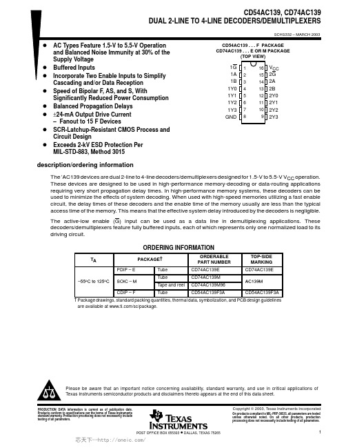
PACKAGING INFORMATIONOrderable Device Status (1)Package Type Package DrawingPins Package Qty Eco Plan (2)Lead/Ball FinishMSL Peak Temp (3)CD54AC139F3A ACTIVE CDIP J 161TBD A42N /A for Pkg Type CD74AC139E ACTIVE PDIP N 1625Pb-Free (RoHS)CU NIPDAU N /A for Pkg Type CD74AC139EE4ACTIVE PDIP N 1625Pb-Free (RoHS)CU NIPDAU N /A for Pkg Type CD74AC139M ACTIVE SOIC D 1640Green (RoHS &no Sb/Br)CU NIPDAU Level-1-260C-UNLIM CD74AC139M96ACTIVE SOIC D 162500Green (RoHS &no Sb/Br)CU NIPDAU Level-1-260C-UNLIM CD74AC139M96E4ACTIVE SOIC D 162500Green (RoHS &no Sb/Br)CU NIPDAU Level-1-260C-UNLIM CD74AC139M96G4ACTIVE SOIC D 162500Green (RoHS &no Sb/Br)CU NIPDAU Level-1-260C-UNLIM CD74AC139ME4ACTIVE SOIC D 1640Green (RoHS &no Sb/Br)CU NIPDAU Level-1-260C-UNLIM CD74AC139MG4ACTIVESOICD1640Green (RoHS &no Sb/Br)CU NIPDAULevel-1-260C-UNLIM(1)The marketing status values are defined as follows:ACTIVE:Product device recommended for new designs.LIFEBUY:TI has announced that the device will be discontinued,and a lifetime-buy period is in effect.NRND:Not recommended for new designs.Device is in production to support existing customers,but TI does not recommend using this part in a new design.PREVIEW:Device has been announced but is not in production.Samples may or may not be available.OBSOLETE:TI has discontinued the production of the device.(2)Eco Plan -The planned eco-friendly classification:Pb-Free (RoHS),Pb-Free (RoHS Exempt),or Green (RoHS &no Sb/Br)-please check /productcontent for the latest availability information and additional product content details.TBD:The Pb-Free/Green conversion plan has not been defined.Pb-Free (RoHS):TI's terms "Lead-Free"or "Pb-Free"mean semiconductor products that are compatible with the current RoHS requirements for all 6substances,including the requirement that lead not exceed 0.1%by weight in homogeneous materials.Where designed to be soldered at high temperatures,TI Pb-Free products are suitable for use in specified lead-free processes.Pb-Free (RoHS Exempt):This component has a RoHS exemptionfor either 1)lead-based flip-chip solder bumps used between the die and package,or 2)lead-based die adhesive used between the die and leadframe.The component is otherwise considered Pb-Free (RoHS compatible)as defined above.Green (RoHS &no Sb/Br):TI defines "Green"to mean Pb-Free (RoHS compatible),and free of Bromine (Br)and Antimony (Sb)based flame retardants (Br or Sb do not exceed 0.1%by weight in homogeneous material)(3)MSL,Peak Temp.--The Moisture Sensitivity Level rating according to the JEDEC industry standard classifications,and peak solder temperature.Important Information and Disclaimer:The information provided on this page represents TI's knowledge and belief as of the date that it is provided.TI bases its knowledge and belief on information provided by third parties,and makes no representation or warranty as to the accuracy of such information.Efforts are underway to better integrate information from third parties.TI has taken and continues to take reasonable steps to provide representative and accurate information but may not have conducted destructive testing or chemical analysis on incoming materials and chemicals.TI and TI suppliers consider certain information to be proprietary,and thus CAS numbers and other limited information may not be available for release.In no event shall TI's liability arising out of such information exceed the total purchase price of the TI part(s)at issue in this document sold by TI to Customer on an annual basis.PACKAGE OPTION ADDENDUM15-Oct-2009TAPE AND REEL INFORMATION*All dimensions are nominalDevicePackage Type Package Drawing Pins SPQReel Diameter (mm)Reel Width W1(mm)A0(mm)B0(mm)K0(mm)P1(mm)W (mm)Pin1Quadrant CD74AC139M96SOICD162500330.016.46.510.3 2.18.016.0Q1*All dimensions are nominalDevice Package Type Package Drawing Pins SPQ Length(mm)Width(mm)Height(mm) CD74AC139M96SOIC D162500333.2345.928.6IMPORTANT NOTICETexas Instruments Incorporated and its subsidiaries(TI)reserve the right to make corrections,modifications,enhancements,improvements, and other changes to its products and services at any time and to discontinue any product or service without notice.Customers should obtain the latest relevant information before placing orders and should verify that such information is current and complete.All products are sold subject to TI’s terms and conditions of sale supplied at the time of order acknowledgment.TI warrants performance of its hardware products to the specifications applicable at the time of sale in accordance with TI’s standard warranty.Testing and other quality control techniques are used to the extent TI deems necessary to support this warranty.Except where mandated by government requirements,testing of all parameters of each product is not necessarily performed.TI assumes no liability for applications assistance or customer product design.Customers are responsible for their products and applications using TI components.To minimize the risks associated with customer products and applications,customers should provide adequate design and operating safeguards.TI does not warrant or represent that any license,either express or implied,is granted under any TI patent right,copyright,mask work right, or other TI intellectual property right relating to any combination,machine,or process in which TI products or services are rmation published by TI regarding third-party products or services does not constitute a license from TI to use such products or services or a warranty or endorsement e of such information may require a license from a third party under the patents or other intellectual property of the third party,or a license from TI under the patents or other intellectual property of TI.Reproduction of TI information in TI data books or data sheets is permissible only if reproduction is without alteration and is accompanied by all associated warranties,conditions,limitations,and notices.Reproduction of this information with alteration is an unfair and deceptive business practice.TI is not responsible or liable for such altered rmation of third parties may be subject to additional restrictions.Resale of TI products or services with statements different from or beyond the parameters stated by TI for that product or service voids all express and any implied warranties for the associated TI product or service and is an unfair and deceptive business practice.TI is not responsible or liable for any such statements.TI products are not authorized for use in safety-critical applications(such as life support)where a failure of the TI product would reasonably be expected to cause severe personal injury or death,unless officers of the parties have executed an agreement specifically governing such use.Buyers represent that they have all necessary expertise in the safety and regulatory ramifications of their applications,and acknowledge and agree that they are solely responsible for all legal,regulatory and safety-related requirements concerning their products and any use of TI products in such safety-critical applications,notwithstanding any applications-related information or support that may be provided by TI.Further,Buyers must fully indemnify TI and its representatives against any damages arising out of the use of TI products in such safety-critical applications.TI products are neither designed nor intended for use in military/aerospace applications or environments unless the TI products are specifically designated by TI as military-grade or"enhanced plastic."Only products designated by TI as military-grade meet military specifications.Buyers acknowledge and agree that any such use of TI products which TI has not designated as military-grade is solely at the Buyer's risk,and that they are solely responsible for compliance with all legal and regulatory requirements in connection with such use. TI products are neither designed nor intended for use in automotive applications or environments unless the specific TI products are designated by TI as compliant with ISO/TS16949requirements.Buyers acknowledge and agree that,if they use any non-designated products in automotive applications,TI will not be responsible for any failure to meet such requirements.Following are URLs where you can obtain information on other Texas Instruments products and application solutions:Products ApplicationsAudio /audio Communications and Telecom /communicationsAmplifiers Computers and Peripherals /computersData Converters Consumer Electronics /consumer-appsDLP®Products Energy and Lighting /energyDSP Industrial /industrialClocks and Timers /clocks Medical /medicalInterface Security /securityLogic Space,Avionics and Defense /space-avionics-defense Power Mgmt Transportation and /automotiveAutomotiveMicrocontrollers Video and Imaging /videoRFID Wireless /wireless-appsRF/IF and ZigBee®Solutions /lprfTI E2E Community Home Page Mailing Address:Texas Instruments,Post Office Box655303,Dallas,Texas75265Copyright©2011,Texas Instruments Incorporated。
proteus常用元件中英文对照表元件名称中文名说明
proteus常用元件中英文对照表元件名称中文名说明元件名称中文名说明7407 驱动门1N914 二极管74Ls00 与非门74LS04 非门74LS08 与门74LS390 TTL 双十进制计数器7SEG 4针BCD-LED 输出从0-9 对应于4根线的BCD码7SEG 3-8译码器电路BCD-7SEG[size=+0]转换电路ALTERNATOR 交流发电机AMMETER-MILLI mA安培计AND 与门BA TTERY 电池/电池组BUS 总线CAP 电容CAPACITOR 电容器CLOCK 时钟信号源CRYSTAL 晶振D-FLIPFLOP D触发器FUSE 保险丝GROUND 地LAMP 灯LED-RED 红色发光二极管LM016L 2行16列液晶可显示2行16列英文字符,有8位数据总线D0-D7,RS,R/W,EN三个控制端口(共14线),工作电压为5V。
没背光,和常用的1602B功能和引脚一样(除了调背光的二个线脚)矚慫润厲钐瘗睞枥庑赖賃軔朧。
LOGIC ANAL YSER 逻辑分析器LOGICPROBE 逻辑探针LOGICPROBE[BIG] 逻辑探针用来显示连接位置的逻辑状态LOGICSTATE 逻辑状态用鼠标点击,可改变该方框连接位置的逻辑状态LOGICTOGGLE 逻辑触发MASTERSWITCH 按钮手动闭合,立即自动打开MOTOR 马达OR 或门POT-LIN 三引线可变电阻器POWER 电源RES 电阻RESISTOR 电阻器SWITCH 按钮手动按一下一个状态SWITCH-SPDT 二选通一按钮VOLTMETER 伏特计VOLTMETER-MILLI mV伏特计VTERM 串行口终端Electromechanical 电机Inductors 变压器Laplace Primitives 拉普拉斯变换Memory IcsMicroprocessor IcsMiscellaneous 各种器件AERIAL-天线;ATAHDD;ATMEGA64;BATTERY;CELL;CRYSTAL-晶振;FUSE;METER-仪表;聞創沟燴鐺險爱氇谴净祸測樅。
HD74AC182中文资料
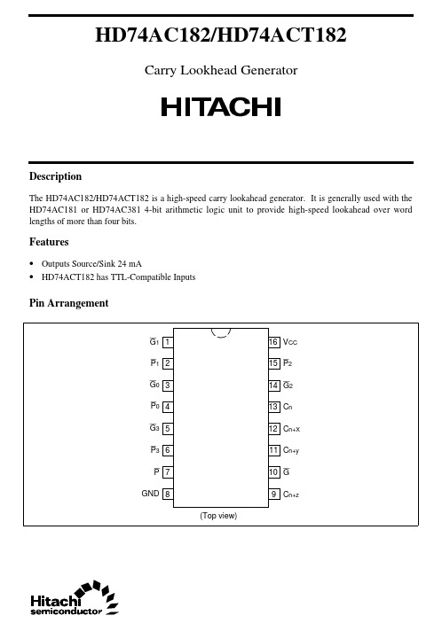
HD74AC182/HD74ACT182Carry Lookhead GeneratorDescriptionThe HD74AC182/HD74ACT182 is a high-speed carry lookahead generator. It is generally used with the HD74AC181 or HD74AC381 4-bit arithmetic logic unit to provide high-speed lookahead over word lengths of more than four bits.Features• Outputs Source/Sink 24 mA• HD74ACT182 has TTL-Compatible InputsPin ArrangementHD74AC182/HD74ACT1822Logic SymbolPin NamesCn Carry InputG 0, G 2Carry Generate Inputs (Active Low)G 1Carry Generate Input (Active Low)G 3Carry Generate Input (Active Low)P 0, P 1Carry Propagate Inputs (Active Low)P 2Carry Propagate Input (Active Low)P 3Carry Propagate Input (Active Low)C n + x to C n + z Carry OutputsG Carry Generate Output (Active Low)PCarry Propagate Output (Active Low)HD74AC182/HD74ACT1823Logic DiagramFunctional DescriptionThe HD74AC182/HD74ACT182 carry lookahead generator accepts up to four pairs of Active Low Carry Propagate (P 0 to P 3) and Carry Generate (G 0 to G 3) signals and an Active High Carry input (Cn) and provides anticipated Active High carries (C n + x , C n + y , C n + z ) across four groups of binary adders. The HD74AC182/HD74ACT182 also has Active Low Carry Propagate (P ) and Carry Generate (G ) outputs which may be used for further level of lookahead. The logic equations provided at the outputs are:C n + x = G 0 + P 0C nC n + y = G 1 + P 1G 0 + P 1P 0C nC n + z = G 2 + P 2G 1 + P 2P 1G 0 + P 2P 1P 0C n G =G 3 + P 3G 2 + P 3P 2G 1 + P 3P 2P 1G 0P =P 3P 2P 1P 0Also, the HD74AC182/HD74ACT182 can be used with binary ALUs in an active Low or active High input operand mode. The connections (Figure a) to and from the ALU to the carry lookahead generator are identical in both cases. Carries are rippled between lookahead blocks. The critical speed path follows the circled numbers. There are several possible arrangements for the carry interconnects, but all achieve about the same speed. A 28-bit ALU is formed by dropping the last HD74AC182/HD74ACT182.HD74AC182/HD74ACT1824Truth TableInputs Outputs C n G 0P 0G 1P 1G 2P 2G 3P 3C n + x C n + yC n + zGPX H H L L H X L X L X H H X L HX X X H H L X H H H X L L H X H X L X X X L X H X L X X L H H X L X L HX X X X X H H L X X X H H H X L X H H H X H X L L H X H X H X L X X X X X L X H X X X L X X L H X L X X L X L H HX LX L X L HX X X X X H H H X X X H H H X H X H H H X H X H H H X H X H X H X X X X X L X L X X X L X X L L X L X X L X L L LXL XL XL LH X X X H X H X X H X X H X H X X X H H LLLLLH :High Voltage Level L :Low Voltage Level X :ImmaterialHD74AC182/HD74ACT1825DC Characteristics (unless otherwise specified)ItemSymbol Max Unit ConditionMaximum quiescent supply current I CC 80µA V IN = V CC or ground, V CC = 5.5 V,Ta = Worst caseMaximum quiescent supply current I CC 8.0µA V IN = V CC or ground, V CC = 5.5 V,Ta = 25°CMaximum I CC /input (HD74ACT182)I CCT1.5mAV IN = V CC – 2.1 V, V CC = 5.5 V,Ta = Worst caseAC Characteristics: HD74AC182Ta = +25°C C L = 50 pFTa = –40°C to +85°C C L = 50 pF ItemSymbol V CC (V)*1Min Typ Max Min Max Unit Propagation delay t PLH3.3 1.08.010.5 1.011.5nsP n to P5.0 1.0 5.58.0 1.09.0Propagation delay t PHL 3.3 1.08.010.5 1.011.5ns P n to P5.0 1.0 5.58.0 1.09.0Propagation delay t PLH 3.3 1.09.512.0 1.013.0ns C n to C n + x, y, z5.0 1.07.510.0 1.011.0Propagation delay t PHL 3.3 1.09.012.0 1.013.0ns C n to C n + x, y, z5.0 1.07.010.0 1.011.0Propagation delay t PLH 3.3 1.010.513.0 1.014.0ns P n or G n to C n + x, y, z 5.0 1.08.010.5 1.011.5Propagation delay t PHL 3.3 1.011.514.0 1.015.5ns P n or G n to C n + x, y, z 5.01.09.011.51.012.5Note:1.Voltage Range 3.3 is 3.3 V ± 0.3 VVoltage Range 5.0 is 5.0 V ± 0.5 VHD74AC182/HD74ACT1826AC Characteristics: HD74ACT182Ta = +25°C C L = 50 pFTa = –40°C to +85°C C L = 50 pF ItemSymbol V CC (V)*1Min Typ Max Min Max Unit Propagation delay P n to Pt PLH 5.0 1.07.09.0 1.010.0ns Propagation delay P n to Pt PHL 5.0 1.08.010.0 1.011.0ns Propagation delay C n to C n + x, y, zt PLH 5.0 1.09.011.0 1.012.0ns Propagation delay C n to C n + x, y, zt PHL 5.0 1.09.011.0 1.012.0ns Propagation delay P n or G n to C n + x, y, z t PLH 5.0 1.09.011.0 1.012.0ns Propagation delay P n or G n to C n + x, y, z t PHL5.01.010.012.51.013.5nsNote:1.Voltage Range 5.0 is 5.0 V ± 0.5 VCapacitanceItemSymbol Typ Unit Condition Input capacitanceC IN 4.5pF V CC = 5.5 V Power dissipation capacitanceC PD50.0pFV CC = 5.0 VHitachi CodeJEDECEIAJWeight (reference value)DP-16 Conforms Conforms 1.07 gHitachi Code JEDEC EIAJWeight (reference value)FP-16DA —Conforms 0.24 g*Dimension including the plating thicknessBase material dimension° – 8°Hitachi CodeJEDECEIAJWeight (reference value)FP-16DN Conforms Conforms 0.15 g*Dimension including the plating thickness Base material dimension° – 8°Hitachi CodeJEDECEIAJWeight (reference value)TTP-16DA ——0.05 g*Dimension including the plating thickness Base material dimensionCautions 1.Hitachi neither warrants nor grants licenses of any rights of Hitachi’s or any third party’s patent,copyright, trademark, or other intellectual property rights for information contained in this document.Hitachi bears no responsibility for problems that may arise with third party’s rights, includingintellectual property rights, in connection with use of the information contained in this document.2.Products and product specifications may be subject to change without notice. Confirm that you havereceived the latest product standards or specifications before final design, purchase or use.3.Hitachi makes every attempt to ensure that its products are of high quality and reliability. However,contact Hitachi’s sales office before using the product in an application that demands especially high quality and reliability or where its failure or malfunction may directly threaten human life or cause risk of bodily injury, such as aerospace, aeronautics, nuclear power, combustion control, transportation,traffic, safety equipment or medical equipment for life support.4.Design your application so that the product is used within the ranges guaranteed by Hitachi particularlyfor maximum rating, operating supply voltage range, heat radiation characteristics, installationconditions and other characteristics. Hitachi bears no responsibility for failure or damage when used beyond the guaranteed ranges. Even within the guaranteed ranges, consider normally foreseeable failure rates or failure modes in semiconductor devices and employ systemic measures such as fail-safes, so that the equipment incorporating Hitachi product does not cause bodily injury, fire or other consequential damage due to operation of the Hitachi product.5.This product is not designed to be radiation resistant.6.No one is permitted to reproduce or duplicate, in any form, the whole or part of this document withoutwritten approval from Hitachi.7.Contact Hitachi’s sales office for any questions regarding this document or Hitachi semiconductorproducts.Hitachi, Ltd.Semiconductor & Integrated Circuits.Nippon Bldg., 2-6-2, Ohte-machi, Chiyoda-ku, Tokyo 100-0004, Japan Tel: Tokyo (03) 3270-2111 Fax: (03) 3270-5109Copyright ' Hitachi, Ltd., 1999. All rights reserved. Printed in Japan.Hitachi Asia Pte. Ltd.16 Collyer Quay #20-00Hitachi Tower Singapore 049318Tel: 535-2100Fax: 535-1533URL NorthAmerica : http:/Europe : /hel/ecg Asia (Singapore): .sg/grp3/sicd/index.htm Asia (Taiwan): /E/Product/SICD_Frame.htm Asia (HongKong): /eng/bo/grp3/index.htm Japan : http://www.hitachi.co.jp/Sicd/indx.htmHitachi Asia Ltd.Taipei Branch Office 3F, Hung Kuo Building. No.167, Tun-Hwa North Road, Taipei (105)Tel: <886> (2) 2718-3666Fax: <886> (2) 2718-8180Hitachi Asia (Hong Kong) Ltd.Group III (Electronic Components)7/F., North Tower, World Finance Centre,Harbour City, Canton Road, Tsim Sha Tsui,Kowloon, Hong Kong Tel: <852> (2) 735 9218Fax: <852> (2) 730 0281 Telex: 40815 HITEC HXHitachi Europe Ltd.Electronic Components Group.Whitebrook ParkLower Cookham RoadMaidenheadBerkshire SL6 8YA, United KingdomTel: <44> (1628) 585000Fax: <44> (1628) 778322Hitachi Europe GmbH Electronic components Group Dornacher Stra§e 3D-85622 Feldkirchen, Munich Germany Tel: <49> (89) 9 9180-0Fax: <49> (89) 9 29 30 00Hitachi Semiconductor(America) Inc.179 East Tasman Drive,San Jose,CA 95134Tel: <1> (408) 433-1990Fax: <1>(408) 433-0223For further information write to:。
DM74LS169中文资料
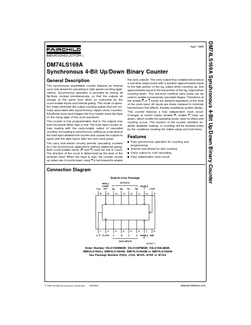
DM74LS169ASynchronous 4-Bit Up/Down Binary CounterGeneral DescriptionThis synchronous presettable counter features an internal carry look-ahead for cascading in high-speed counting appli-cations.Synchronous operation is provided by having all flip-flops clocked simultaneously,so that the outputs all change at the same time when so instructed by the count-enable inputs and internal gating.This mode of opera-tion helps eliminate the output counting spikes that are nor-mally associated with asynchronous (ripple clock)counters.A buffered clock input triggers the four master-slave flip-flops on the rising edge of the clock waveform.This counter is fully programmable;that is,the outputs may each be preset either high or low.The load input circuitry al-lows loading with the carry-enable output of cascaded counters.As loading is synchronous,setting up a low level at the load input disables the counter and causes the outputs to agree with the data inputs after the next clock pulse.The carry look-ahead circuitry permits cascading counters for n-bit synchronous applications without additional gating.Both count-enable inputs (P and T)must be low to count.The direction of the count is determined by the level of the up/down input.When the input is high,the counter counts up;when low,it counts down.Input T is fed forward to enablethe carry outputs.The carry output thus enabled will produce a low-level output pulse with a duration approximately equal to the high portion of the Q A output when counting up,and approximately equal to the low portion of the Q A output when counting down.This low-level overflow carry pulse can be used to enable successively cascaded stages.Transitions at the enable P or T inputs are allowed regardless of the level of the clock input.All inputs are diode clamped to minimize transmission-line effects,thereby simplifying system design.This counter features a fully independent clock circuit.Changes at control inputs (enable P,enable T,load,up/down),which modify the operating mode,have no effect until clocking occurs.The function of the counter (whether en-abled,disabled,loading,or counting)will be dictated solely by the conditions meeting the stable setup and hold times.Featuresn Fully synchronous operation for counting and programming.n Internal look-ahead for fast counting.n Carry output for n-bit cascading.n Fully independent clock circuitConnection DiagramDual-In-Line PackageDS006401-1Order Number 54LS169DMQB,54LS169FMQB,54LS169LMQB,DM54LS169AJ,DM54LS169AW,DM74LS169AM or DM74LS169ANSee Package Number E20A,J16A,M16A,N16E or W16AApril 1998DM74LS169A Synchronous 4-Bit Up/Down Binary Counter©1998Fairchild Semiconductor Corporation Absolute Maximum Ratings(Note1)Supply Voltage7V Input Voltage7V Operating Free Air Temperature RangeDM54LS and54LS−55˚C to+125˚C DM74LS0˚C to+70˚C Storage Temperature Range−65˚C to+150˚CRecommended Operating ConditionsSymbol Parameter DM54LS169A DM74LS169A UnitsMin Nom Max Min Nom MaxV CC Supply Voltage 4.55 5.5 4.755 5.25V V IH High Level Input Voltage22V V IL Low Level Input Voltage0.70.8V I OH High Level Output Current−0.4−0.4mA I OL Low Level Output Current48mA f CLK Clock Frequency(Note2)025025MHzClock Frequency(Note3)020020MHz t W Clock Pulse Width(Note4)2525ns t SU Setup Time Data2020(Note4)Enable2020T or P nsLoad2525U/D3030t H Hold Time(Note4)00ns T A Free Air Operating Temperature−55125070˚C Note1:The“Absolute Maximum Ratings”are those values beyond which the safety of the device cannot be guaranteed.The device should not be operated at these limits.The parametric values defined in the“Electrical Characteristics”table are not guaranteed at the absolute maximum ratings.The“Recommended Operating Conditions”table will define the conditions for actual device operation.Note2:C L=15pF,R L=2kΩ,T A=25˚C and V CC=5V.Note3:C L=50pF,R L=2kΩ,T A=25˚C and V CC=5V.Note4:T A=25˚C and V CC=5V.Electrical Characteristicsover recommended operating free air temperature range(unless otherwise noted)Symbol Parameter Conditions Min Typ Max Units(Note5)V I Input Clamp Voltage V CC=Min,I I=−18mA−1.5V V OH High Level Output V CC=Min,I OH=Max DM54 2.5 3.4V Voltage V IL=Max,V IH=Min DM74 2.7 3.4V OL Low Level Output V CC=Min,I OL=Max DM540.250.4 Voltage V IL=Max,V IH=Min DM740.350.5VI OL=4mA,V CC=Min DM740.250.4I I Input Current@Max V CC=Max Enable T0.2mAInput Voltage V I=7V Others0.1I IH High Level Input V CC=Max Enable T40µACurrent V I=2.7V Others20I IL Low Level Input V CC=Max Enable T−0.8mACurrent V I=0.4V Others−0.4I OS Short Circuit V CC=Max DM54−20−100mAOutput Current(Note6)DM74−20−100I CC Supply Current V CC=Max(Note7)2034mANote5:All typicals are at V CC=5V and T A=25˚C.Note6:Not more than one output should be shorted at a time,and the duration should not exceed one second.Note7:I CC is measured after a momentary4.5V,then ground,is applied to the CLOCK with all other inputs grounded and all the outputs open.2Switching Characteristicat V CC=5V and T A=25˚C(for Test Waveforms and Output Load)From(Input)R L=2kΩSymbol Parameter To(Output)C L=15pF C L=50pF UnitsMin Max Min Maxf MAX Maximum Clock2520MHzFrequencyt PLH Propagation Delay Time Clock to3539ns Low to High Level Output Ripple Carryt PHL Propagation Delay Time Clock to3544ns High to Low Level Output Ripple Carryt PLH Propagation Delay Time Clock to2024ns Low to High Level Output Any Qt PHL Propagation Delay Time Clock to2332ns High to Low Level Output Any Qt PLH Propagation Delay Time Enable T to1824ns Low to High Level Output Ripple Carryt PHL Propagation Delay Time Enable T to1828ns High to Low Level Output Ripple Carryt PLH Propagation Delay Time Up/Down to2530ns Low to High Level Output Ripple Carry(Note8)t PHL Propagation Delay Time Up/Down to2938ns High to Low Level Output Ripple Carry(Note8)Note8:The propagation delay from UP/DOWN to RIPPLE CARRY must be measured with the counter at either a minimum or a maximum count.As the logic levelof the up/down input is changed,the ripple carry output will follow.If the count is minimum,the ripple carry output transition will be in phase.If the count is maximum,the ripple carry output will be out of phase.Logic DiagramLS169A Binary CounterDS006401-2 4Timing DiagramLS169A Binary CountersTypical Load,Count,and Inhibit SequencesDS006401-3Physical Dimensions inches(millimeters)unless otherwise notedCeramic Leadless Chip Carrier Package(E)Order Number54LS169LMQBPackage Number E20A16-Lead Ceramic Dual-In-Line Package(J)Order Number54LS169DMQB or DM54LS169AJPackage Number J16A6Physical Dimensions inches(millimeters)unless otherwise noted(Continued)16-Lead Small Outline Molded Package(M)Order Number DM74LS169AMPackage Number M16A16-Lead Molded Dual-In-Line Package(N)Order Number DM74LS169ANPackage Number N16EPhysical Dimensionsinches (millimeters)unless otherwise noted (Continued)LIFE SUPPORT POLICYFAIRCHILD’S PRODUCTS ARE NOT AUTHORIZED FOR USE AS CRITICAL COMPONENTS IN LIFE SUPPORT DE-VICES OR SYSTEMS WITHOUT THE EXPRESS WRITTEN APPROVAL OF THE PRESIDENT OF FAIRCHILD SEMI-CONDUCTOR CORPORATION.As used herein:1.Life support devices or systems are devices or sys-tems which,(a)are intended for surgical implant intothe body,or (b)support or sustain life,and (c)whosefailure to perform when properly used in accordancewith instructions for use provided in the labeling,can be reasonably expected to result in a significant injury to the user.2.A critical component in any component of a life support device or system whose failure to perform can be rea-sonably expected to cause the failure of the life support device or system,or to affect its safety or effectiveness.Fairchild Semiconductor Corporation AmericasCustomer Response Center Tel:1-888-522-5372Fairchild Semiconductor EuropeFax:+49(0)180-5308586Email:europe.support@Deutsch Tel:+49(0)8141-35-0English Tel:+44(0)1793-85-68-56Italy Tel:+39(0)2575631Fairchild SemiconductorHong Kong Ltd.13th Floor,Straight Block,Ocean Centre,5Canton Rd.Tsimshatsui,Kowloon Hong KongTel:+8522737-7200Fax:+8522314-0061National Semiconductor Japan Ltd.Tel:81-3-5620-6175Fax:81-3-5620-617916-Lead Ceramic Flat Package (W)Order Number 54LS169FMQB or DM54LS169AWPackage Number W16AD M 74L S 169A S y n c h r o n o u s 4-B i t U p /D o w n B i n a r y C o u n t e rFairchild does not assume any responsibility for use of any circuitry described,no circuit patent licenses are implied and Fairchild reserves the right at any time without notice to change said circuitry and specifications.。
SN74AC74PWE4中文资料
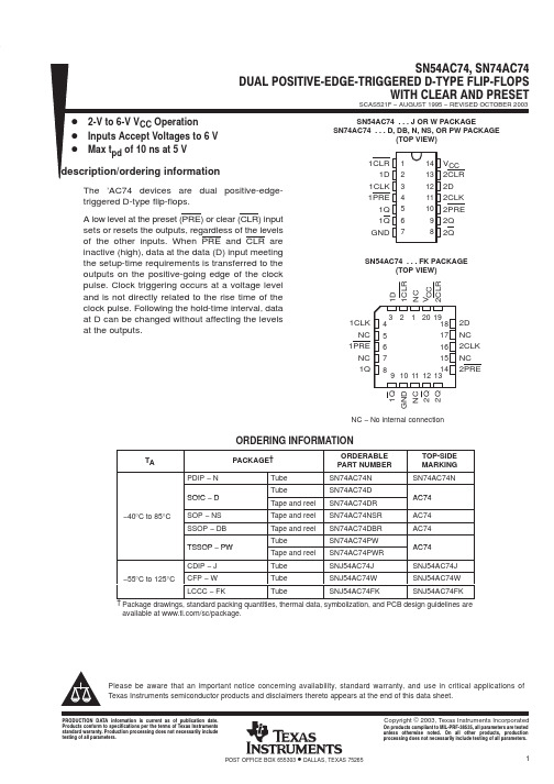
PACKAGING INFORMATIONOrderable Device Status (1)Package Type Package Drawing Pins Package Qty Eco Plan (2)Lead/Ball FinishMSL Peak Temp (3)5962-88520012A ACTIVE LCCC FK 201TBD POST-PLATE N /A for Pkg Type 5962-8852001CA ACTIVE CDIP J 141TBD A42SNPB N /A for Pkg Type 5962-8852001DA ACTIVE CFPW 141TBD A42N /A for Pkg Type 5962-8852001VCA ACTIVE CDIP J 141TBD A42SNPB N /A for Pkg Type 5962-8852001VDA ACTIVE CFP W 141TBD A42N /A for Pkg Type SN74AC74D ACTIVE SOIC D 1450Green (RoHS &no Sb/Br)CU NIPDAU Level-1-260C-UNLIM SN74AC74DBLE OBSOLETE SSOP DB 14TBDCall TI Call TISN74AC74DBR ACTIVE SSOP DB 142000Green (RoHS &no Sb/Br)CU NIPDAU Level-1-260C-UNLIM SN74AC74DBRE4ACTIVE SSOP DB 142000Green (RoHS &no Sb/Br)CU NIPDAU Level-1-260C-UNLIM SN74AC74DE4ACTIVE SOIC D 1450Green (RoHS &no Sb/Br)CU NIPDAU Level-1-260C-UNLIM SN74AC74DG4ACTIVE SOIC D 1450Green (RoHS &no Sb/Br)CU NIPDAU Level-1-260C-UNLIM SN74AC74DR ACTIVE SOIC D 142500Green (RoHS &no Sb/Br)CU NIPDAU Level-1-260C-UNLIM SN74AC74DRE4ACTIVE SOIC D 142500Green (RoHS &no Sb/Br)CU NIPDAU Level-1-260C-UNLIM SN74AC74DRG4ACTIVE SOIC D 142500Green (RoHS &no Sb/Br)CU NIPDAU Level-1-260C-UNLIM SN74AC74N ACTIVE PDIP N 1425Pb-Free (RoHS)CU NIPDAU N /A for Pkg Type SN74AC74NE4ACTIVE PDIP N 1425Pb-Free (RoHS)CU NIPDAU N /A for Pkg Type SN74AC74NSR ACTIVE SO NS 142000Green (RoHS &no Sb/Br)CU NIPDAU Level-1-260C-UNLIM SN74AC74NSRE4ACTIVE SO NS 142000Green (RoHS &no Sb/Br)CU NIPDAU Level-1-260C-UNLIM SN74AC74PW ACTIVE TSSOP PW 1490Green (RoHS &no Sb/Br)CU NIPDAU Level-1-260C-UNLIM SN74AC74PWE4ACTIVE TSSOP PW 1490Green (RoHS &no Sb/Br)CU NIPDAU Level-1-260C-UNLIM SN74AC74PWLE OBSOLETE TSSOP PW 14TBDCall TI Call TISN74AC74PWR ACTIVE TSSOP PW 142000Green (RoHS &no Sb/Br)CU NIPDAU Level-1-260C-UNLIM SN74AC74PWRE4ACTIVE TSSOP PW 142000Green (RoHS &no Sb/Br)CU NIPDAULevel-1-260C-UNLIMSNJ54AC74FK ACTIVE LCCC FK 201TBD POST-PLATE N /A for Pkg Type SNJ54AC74J ACTIVE CDIP J 141TBD A42SNPB N /A for Pkg Type SNJ54AC74WACTIVECFPW141TBDA42N /A for Pkg Type(1)The marketing status values are defined as follows:ACTIVE:Product device recommended for new designs.LIFEBUY:TI has announced that the device will be discontinued,and a lifetime-buy period is in effect.NRND:Not recommended for new designs.Device is in production to support existing customers,but TI does not recommend using this part in a new design.PREVIEW:Device has been announced but is not in production.Samples may or may not be available.18-Jul-2006OBSOLETE:TI has discontinued the production of the device.(2)Eco Plan -The planned eco-friendly classification:Pb-Free (RoHS),Pb-Free (RoHS Exempt),or Green (RoHS &no Sb/Br)-please check /productcontent for the latest availability information and additional product content details.TBD:The Pb-Free/Green conversion plan has not been defined.Pb-Free (RoHS):TI's terms "Lead-Free"or "Pb-Free"mean semiconductor products that are compatible with the current RoHS requirements for all 6substances,including the requirement that lead not exceed 0.1%by weight in homogeneous materials.Where designed to be soldered at high temperatures,TI Pb-Free products are suitable for use in specified lead-free processes.Pb-Free (RoHS Exempt):This component has a RoHS exemption for either 1)lead-based flip-chip solder bumps used between the die and package,or 2)lead-based die adhesive used between the die and leadframe.The component is otherwise considered Pb-Free (RoHS compatible)as defined above.Green (RoHS &no Sb/Br):TI defines "Green"to mean Pb-Free (RoHS compatible),and free of Bromine (Br)and Antimony (Sb)based flame retardants (Br or Sb do not exceed 0.1%by weight in homogeneous material)(3)MSL,Peak Temp.--The Moisture Sensitivity Level rating according to the JEDEC industry standard classifications,and peak solder temperature.Important Information and Disclaimer:The information provided on this page represents TI's knowledge and belief as of the date that it is provided.TI bases its knowledge and belief on information provided by third parties,and makes no representation or warranty as to the accuracy of such information.Efforts are underway to better integrate information from third parties.TI has taken and continues to take reasonable steps to provide representative and accurate information but may not have conducted destructive testing or chemical analysis on incoming materials and chemicals.TI and TI suppliers consider certain information to be proprietary,and thus CAS numbers and other limited information may not be available for release.In no event shall TI's liability arising out of such information exceed the total purchase price of the TI part(s)at issue in this document sold by TI to Customer on an annualbasis.18-Jul-2006IMPORTANT NOTICETexas Instruments Incorporated and its subsidiaries (TI) reserve the right to make corrections, modifications, enhancements, improvements, and other changes to its products and services at any time and to discontinue any product or service without notice. Customers should obtain the latest relevant information before placing orders and should verify that such information is current and complete. All products are sold subject to TI’s terms and conditions of sale supplied at the time of order acknowledgment.TI warrants performance of its hardware products to the specifications applicable at the time of sale in accordance with TI’s standard warranty. T esting and other quality control techniques are used to the extent TI deems necessary to support this warranty. Except where mandated by government requirements, testing of all parameters of each product is not necessarily performed.TI assumes no liability for applications assistance or customer product design. Customers are responsible for their products and applications using TI components. T o minimize the risks associated with customer products and applications, customers should provide adequate design and operating safeguards.TI does not warrant or represent that any license, either express or implied, is granted under any TI patent right, copyright, mask work right, or other TI intellectual property right relating to any combination, machine, or process in which TI products or services are used. Information published by TI regarding third-party products or services does not constitute a license from TI to use such products or services or a warranty or endorsement thereof. Use of such information may require a license from a third party under the patents or other intellectual property of the third party, or a license from TI under the patents or other intellectual property of TI.Reproduction of information in TI data books or data sheets is permissible only if reproduction is without alteration and is accompanied by all associated warranties, conditions, limitations, and notices. Reproduction of this information with alteration is an unfair and deceptive business practice. TI is not responsible or liable for such altered documentation.Resale of TI products or services with statements different from or beyond the parameters stated by TI for that product or service voids all express and any implied warranties for the associated TI product or service and is an unfair and deceptive business practice. TI is not responsible or liable for any such statements. Following are URLs where you can obtain information on other Texas Instruments products and application solutions:Products ApplicationsAmplifiers Audio /audioData Converters Automotive /automotiveDSP Broadband /broadbandInterface Digital Control /digitalcontrolLogic Military /militaryPower Mgmt Optical Networking /opticalnetwork Microcontrollers Security /securityLow Power Wireless /lpw Telephony /telephonyVideo & Imaging /videoWireless /wirelessMailing Address:Texas InstrumentsPost Office Box 655303 Dallas, Texas 75265Copyright 2006, Texas Instruments Incorporated。
74及其他系列芯片引脚图资料大全
一:分类74ls00 2输入四与非门74ls01 2输入四与非门(oc)74ls02 2输入四或非门74ls03 2输入四与非门(oc)74ls04 六倒相器74ls05 六倒相器(oc)74ls06 六高压输出反相缓冲器/驱动器(oc,30v) 74ls07 六高压输出缓冲器/驱动器(oc,30v)74ls08 2输入四与门74ls09 2输入四与门(oc)74ls10 3输入三与非门74ls11 3输入三与门74ls12 3输入三与非门(oc)74ls13 4输入双与非门(斯密特触发)74ls14 六倒相器(斯密特触发)74ls15 3输入三与门(oc)74ls16 六高压输出反相缓冲器/驱动器(oc,15v) 74ls17 六高压输出缓冲器/驱动器(oc,15v)74ls18 4输入双与非门(斯密特触发)74ls19 六倒相器(斯密特触发)74ls20 4输入双与非门74ls21 4输入双与门74ls22 4输入双与非门(oc)74ls23 双可扩展的输入或非门74ls24 2输入四与非门(斯密特触发)74ls25 4输入双或非门(有选通)74ls26 2输入四高电平接口与非缓冲器(oc,15v) 74ls27 3输入三或非门74ls28 2输入四或非缓冲器74ls30 8输入与非门74ls31 延迟电路74ls32 2输入四或门74ls33 2输入四或非缓冲器(集电极开路输出) 74ls34 六缓冲器74ls35 六缓冲器(oc)74ls36 2输入四或非门(有选通)74ls37 2输入四与非缓冲器74ls38 2输入四或非缓冲器(集电极开路输出74ls39 2输入四或非缓冲器(集电极开路输出)74ls40 4输入双与非缓冲器74ls41 bcd-十进制计数器74ls42 4线-10线译码器(bcd输入)74ls43 4线-10线译码器(余3码输入)74ls44 4线-10线译码器(余3葛莱码输入)74ls45 bcd-十进制译码器/驱动器74ls46 bcd-七段译码器/驱动器74ls47 bcd-七段译码器/驱动器74ls48 bcd-七段译码器/驱动器74ls49 bcd-七段译码器/驱动器(oc)74ls50 双二路2-2输入与或非门(一门可扩展)74ls51 双二路2-2输入与或非门74ls51 二路3-3输入,二路2-2输入与或非门74ls52 四路2-3-2-2输入与或门(可扩展)74ls53 四路2-2-2-2输入与或非门(可扩展)74ls53 四路2-2-3-2输入与或非门(可扩展)74ls54 四路2-2-2-2输入与或非门74ls54 四路2-3-3-2输入与或非门74ls54 四路2-2-3-2输入与或非门74ls55 二路4-4输入与或非门(可扩展)74ls60 双四输入与扩展74ls61 三3输入与扩展74ls62 四路2-3-3-2输入与或扩展器74ls63 六电流读出接口门74ls64 四路4-2-3-2输入与或非门74ls65 四路4-2-3-2输入与或非门(oc)74ls70 与门输入上升沿jk触发器74ls71 与输入r-s主从触发器74ls72 与门输入主从jk触发器74ls73 双j-k触发器(带清除端)74ls74 正沿触发双d型触发器(带预置端和清除端) 74ls75 4位双稳锁存器74ls76 双j-k触发器(带预置端和清除端)74ls77 4位双稳态锁存器74ls78 双j-k触发器(带预置端,公共清除端和公共时钟端)74ls80 门控全加器74ls81 16位随机存取存储器74ls82 2位二进制全加器(快速进位)74ls83 4位二进制全加器(快速进位)74ls84 16位随机存取存储器74ls85 4位数字比较器74ls86 2输入四异或门74ls87 四位二进制原码/反码/oi单元74ls89 64位读/写存储器74ls90 十进制计数器74ls91 八位移位寄存器74ls92 12分频计数器(2分频和6分频)74ls93 4位二进制计数器74ls94 4位移位寄存器(异步)74ls95 4位移位寄存器(并行io)74ls96 5位移位寄存器74ls97 六位同步二进制比率乘法器74ls100 八位双稳锁存器74ls103 负沿触发双j-k主从触发器(带清除端) 74ls106 负沿触发双j-k主从触发器(带预置,清除,时钟)74ls107 双j-k主从触发器(带清除端)74ls108 双j-k主从触发器(带预置,清除,时钟) 74ls109 双j-k触发器(带置位,清除,正触发)74ls110 与门输入j-k主从触发器(带锁定)74ls111 双j-k主从触发器(带数据锁定)74ls112 负沿触发双j-k触发器(带预置端和清除端)74ls113 负沿触发双j-k触发器(带预置端)74ls114 双j-k触发器(带预置端,共清除端和时钟端)74ls116 双四位锁存器74ls120 双脉冲同步器/驱动器74ls121 单稳态触发器(施密特触发)74ls122 可再触发单稳态多谐振荡器(带清除端) 74ls123 可再触发双单稳多谐振荡器74ls125 四总线缓冲门(三态输出)74ls126 四总线缓冲门(三态输出)74ls128 2输入四或非线驱动器74ls131 3-8译码器74ls132 2输入四与非门(斯密特触发)74ls133 13输入端与非门74ls134 12输入端与门(三态输出)74ls135 四异或/异或非门74ls136 2输入四异或门(oc)74ls137 八选1锁存译码器/多路转换器74ls138 3-8线译码器/多路转换器74ls139 双2-4线译码器/多路转换器74ls140 双4输入与非线驱动器74ls141 bcd-十进制译码器/驱动器74ls142 计数器/锁存器/译码器/驱动器74ls145 4-10译码器/驱动器74ls147 10线-4线优先编码器74ls148 8线-3线八进制优先编码器74ls150 16选1数据选择器(反补输出)74ls151 8选1数据选择器(互补输出)74ls152 8选1数据选择器多路开关74ls153 双4选1数据选择器/多路选择器74ls154 4线-16线译码器74ls155 双2-4译码器/分配器(图腾柱输出)74ls156 双2-4译码器/分配器(集电极开路输出) 74ls157 四2选1数据选择器/多路选择器74ls158 四2选1数据选择器(反相输出)74ls160 可预置bcd计数器(异步清除)74ls161 可预置四位二进制计数器(并清除异步) 74ls162 可预置bcd计数器(异步清除)74ls163 可预置四位二进制计数器(并清除异步) 74ls164 8位并行输出串行移位寄存器74ls165 并行输入8位移位寄存器(补码输出) 74ls166 8位移位寄存器74ls167 同步十进制比率乘法器74ls168 4位加/减同步计数器(十进制)74ls169 同步二进制可逆计数器74ls170 4*4寄存器堆74ls171 四d触发器(带清除端)74ls172 16位寄存器堆74ls173 4位d型寄存器(带清除端)74ls174 六d触发器74ls175 四d触发器74ls176 十进制可预置计数器74ls177 2-8-16进制可预置计数器74ls178 四位通用移位寄存器74ls179 四位通用移位寄存器74ls180 九位奇偶产生/校验器74ls181 算术逻辑单元/功能发生器74ls182 先行进位发生器74ls183 双保留进位全加器74ls184 bcd-二进制转换器74ls185 二进制-bcd转换器74ls190 同步可逆计数器(bcd,二进制)74ls191 同步可逆计数器(bcd,二进制)74ls192 同步可逆计数器(bcd,二进制)74ls193 同步可逆计数器(bcd,二进制)74ls194 四位双向通用移位寄存器74ls195 四位通用移位寄存器74ls196 可预置计数器/锁存器74ls197 可预置计数器/锁存器(二进制)74ls198 八位双向移位寄存器74ls199 八位移位寄存器74ls210 2-5-10进制计数器74ls213 2-n-10可变进制计数器74ls221 双单稳触发器74ls230 八3态总线驱动器74ls231 八3态总线反向驱动器74ls240 八缓冲器/线驱动器/线接收器(反码三态输出)74ls241 八缓冲器/线驱动器/线接收器(原码三态输出)74ls242 八缓冲器/线驱动器/线接收器74ls243 4同相三态总线收发器74ls244 八缓冲器/线驱动器/线接收器74ls245 八双向总线收发器74ls246 4线-七段译码/驱动器(30v)74ls247 4线-七段译码/驱动器(15v)74ls248 4线-七段译码/驱动器74ls249 4线-七段译码/驱动器74ls251 8选1数据选择器(三态输出)74ls253 双四选1数据选择器(三态输出)74ls256 双四位可寻址锁存器74ls257 四2选1数据选择器(三态输出)74ls258 四2选1数据选择器(反码三态输出) 74ls259 8为可寻址锁存器74ls260 双5输入或非门74ls261 4*2并行二进制乘法器74ls265 四互补输出元件74ls266 2输入四异或非门(oc)74ls270 2048位rom (512位四字节,oc)74ls271 2048位rom (256位八字节,oc)74ls273 八d触发器74ls274 4*4并行二进制乘法器74ls275 七位片式华莱士树乘法器74ls276 四jk触发器74ls278 四位可级联优先寄存器74ls279 四s-r锁存器74ls280 9位奇数/偶数奇偶发生器/较验器74ls281 74ls283 4位二进制全加器74ls290 十进制计数器74ls291 32位可编程模74ls293 4位二进制计数器74ls294 16位可编程模74ls295 四位双向通用移位寄存器74ls298 四-2输入多路转换器(带选通)74ls299 八位通用移位寄存器(三态输出)74ls348 8-3线优先编码器(三态输出)74ls352 双四选1数据选择器/多路转换器74ls353 双4-1线数据选择器(三态输出)74ls354 8输入端多路转换器/数据选择器/寄存器,三态补码输出74ls355 8输入端多路转换器/数据选择器/寄存器,三态补码输出74ls356 8输入端多路转换器/数据选择器/寄存器,三态补码输出74ls357 8输入端多路转换器/数据选择器/寄存器,三态补码输出74ls365 6总线驱动器74ls366 六反向三态缓冲器/线驱动器74ls367 六同向三态缓冲器/线驱动器74ls368 六反向三态缓冲器/线驱动器74ls373 八d锁存器74ls374 八d触发器(三态同相)74ls375 4位双稳态锁存器74ls377 带使能的八d触发器74ls378 六d触发器74ls379 四d触发器74ls381 算术逻辑单元/函数发生器74ls382 算术逻辑单元/函数发生器74ls384 8位*1位补码乘法器74ls385 四串行加法器/乘法器74ls386 2输入四异或门74ls390 双十进制计数器74ls391 双四位二进制计数器74ls395 4位通用移位寄存器74ls396 八位存储寄存器74ls398 四2输入端多路开关(双路输出)74ls399 四-2输入多路转换器(带选通)74ls422 单稳态触发器74ls423 双单稳态触发器74ls440 四3方向总线收发器,集电极开路74ls441 四3方向总线收发器,集电极开路74ls442 四3方向总线收发器,三态输出74ls443 四3方向总线收发器,三态输出74ls444 四3方向总线收发器,三态输出74ls445 bcd-十进制译码器/驱动器,三态输出74ls446 有方向控制的双总线收发器74ls448 四3方向总线收发器,三态输出74ls449 有方向控制的双总线收发器74ls465 八三态线缓冲器74ls466 八三态线反向缓冲器74ls467 八三态线缓冲器74ls468 八三态线反向缓冲器74ls490 双十进制计数器74ls540 八位三态总线缓冲器(反向)74ls541 八位三态总线缓冲器74ls589 有输入锁存的并入串出移位寄存器74ls590 带输出寄存器的8位二进制计数器74ls591 带输出寄存器的8位二进制计数器74ls592 带输出寄存器的8位二进制计数器74ls593 带输出寄存器的8位二进制计数器74ls594 带输出锁存的8位串入并出移位寄存器74ls595 8位输出锁存移位寄存器74ls596 带输出锁存的8位串入并出移位寄存器74ls597 8位输出锁存移位寄存器74ls598 带输入锁存的并入串出移位寄存器74ls599 带输出锁存的8位串入并出移位寄存器74ls604 双8位锁存器74ls605 双8位锁存器74ls606 双8位锁存器74ls607 双8位锁存器74ls620 8位三态总线发送接收器(反相)74ls621 8位总线收发器74ls622 8位总线收发器74ls623 8位总线收发器74ls640 反相总线收发器(三态输出)74ls641 同相8总线收发器,集电极开路74ls642 同相8总线收发器,集电极开路74ls643 8位三态总线发送接收器74ls644 真值反相8总线收发器,集电极开路74ls645 三态同相8总线收发器74ls646 八位总线收发器,寄存器74ls647 八位总线收发器,寄存器74ls648 八位总线收发器,寄存器74ls649 八位总线收发器,寄存器74ls651 三态反相8总线收发器74ls652 三态反相8总线收发器74ls653 反相8总线收发器,集电极开路74ls654 同相8总线收发器,集电极开路74ls668 4位同步加/减十进制计数器74ls669 带先行进位的4位同步二进制可逆计数器74ls670 4*4寄存器堆(三态)74ls671 带输出寄存的四位并入并出移位寄存器74ls672 带输出寄存的四位并入并出移位寄存器74ls673 16位并行输出存储器,16位串入串出移位寄存器74ls674 16位并行输入串行输出移位寄存器74ls681 4位并行二进制累加器74ls682 8位数值比较器(图腾柱输出)74ls683 8位数值比较器(集电极开路)74ls684 8位数值比较器(图腾柱输出)74ls685 8位数值比较器(集电极开路)74ls686 8位数值比较器(图腾柱输出)74ls687 8位数值比较器(集电极开路)74ls688 8位数字比较器(oc输出)74ls689 8位数字比较器74ls690 同步十进制计数器/寄存器(带数选,三态输出,直接清除)74ls691 计数器/寄存器(带多转换,三态输出)74ls692 同步十进制计数器(带预置输入,同步清除) 74ls693 计数器/寄存器(带多转换,三态输出)74ls696 同步加/减十进制计数器/寄存器(带数选,三态输出,直接清除)74ls697 计数器/寄存器(带多转换,三态输出)74ls698 计数器/寄存器(带多转换,三态输出)74ls699 计数器/寄存器(带多转换,三态输出)74ls716 可编程模n十进制计数器74ls718 可编程模n十进制计数器LM12瓦运算放大器LM124 LM224 LM324 LM2902 低电压双路运算放大器LM324 低电压双路运算放大器LM129 LM329 精密电压基准芯片LM135 LM235 LM335 精密温度传感器芯片LM1458 LM1558 双运算放大器LM158 LM258 LM358 LM2904 低压双运算放大器LM18293 四通道推拉驱动器LM1868 调幅/调频收音机芯片LM1951 1安培固态开关LM2574 0.5A降阶式电压调节器LM1575 LM2575 1A 降阶式电压调节器LM2576 3A 3A 降阶式电压调节器LM1577 LM2577 降阶式电压调节器LM2587 5A 返馈开关式电压调节器LM1893 LM2893 载体电流收发器LM193 LM293 LM393 LM2903 双路低压低漂移比较器LM2907 LM2917 频率电压转换器LM101A LM201A LM301A 运算放大器芯片LM3045 LM3046 LM3086 晶体管阵列LM111 LM211 LM311 电压比较器LM117 LM317 三端可调式稳压器LM118 LM218 LM318 运算放大器LM133 LM333安培可调负电压调节器LM137 LM337 可调式三端负压稳压器LM34 精密华氏温度传感器LM342 三端正压稳压器LM148 LM248 LM348 / LM149 LM349 双LM741运算放大器LM35 精密摄氏温度传感器LM158 LM258 LM358 LM2904 低压双运算放大器LM150 LM350 3安培可调式电压调节器LM380 2.5瓦音频放大器LM386 低压音频功率放大器LM3886 高性能68瓦音频功率放大器/带静音LM555 LM555C 时基发生器电路LM556 LM556C 双时基发生器电路LM565 相位跟随器LM567 音频译码器LM621 无刷电机换向器LM628 LM629精密位移控制器LM675功率运算放大器LM723 电压调节器LM741 运算放大器LM7805 LM78xx 系列稳压器LM7812 LM78xx 系列稳压器LM7815 LM78xx 系列稳压器LM78L00 三端正压调节器LM78L05 三端正压调节器LM78L09三端正压调节器LM78L12 三端正压调节器LM78L15 三端正压调节器LM78L62 三端正压调节器LM78L82 三端正压调节器LM340 LM78Mxx 三端正压稳压器LM7905 三端负压调节器LM7912 三端负压调节器LM7915 三端负压调节器LM79Mxx三端负压调节器LF147 LF347 宽带J型场效应输入运算放大器LF351 宽带J型场效应输入运算放大器LF353 宽带J型场效应输入运算放大器LF444 双低压J型场效应输入运算放大器(1) 74LS00双输入四与非门,管脚图如附图1-27所示。
74AC163B中文资料
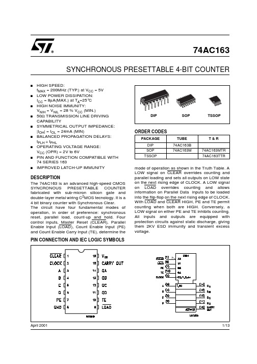
1/13April 2001sHIGH SPEED:f MAX = 200MHz (TYP.) at V CC = 5V sLOW POWER DISSIPATION:I CC = 8µA(MAX.) at T A =25°C sHIGH NOISE IMMUNITY:V NIH = V NIL = 28 % V CC (MIN.)s50Ω TRANSMISSION LINE DRIVING CAPABILITYsSYMMETRICAL OUTPUT IMPEDANCE:|I OH | = I OL = 24mA (MIN)sBALANCED PROPAGATION DELAYS:t PLH ≅ t PHLsOPERATING VOLTAGE RANGE:V CC (OPR) = 2V to 6VsPIN AND FUNCTION COMPATIBLE WITH 74 SERIES 163sIMPROVED LATCH-UP IMMUNITYDESCRIPTIONThe 74AC163 is an advanced high-speed CMOS SYNCRONOUS PRESETTABLE COUNTER fabricated with sub-micron silicon gate and double-layer metal wiring C 2MOS tecnology. It is a 4 bit binary counter with Synchronous Clear.The circuit have four fundamental modes of operation, in order of preference: synchronous reset, parallel load, count-up and hold. Four control inputs, Master Reset (CLEAR), Parallel Enable Input (LOAD), Count Enable Input (PE)and Count Enable Carry Input (TE), determine the mode of operation as shown in the Truth Table. A LOW signal on CLEAR overrides counting and parallel loading and sets all outputs on LOW state on the next rising edge of CLOCK. A LOW signal on LOAD overrides counting and allows information on Parallel Data inputs to be loaded into the flip-flop on the next rising edge of CLOCK.With LOAD and CLEAR HIGH, PE and TE permit counting when both are HIGH. Conversely, a LOW signal on either PE and TE inhibits counting.All inputs and outputs are equipped with protection circuits against static discharge, giving them 2KV ESD immunity and transient excess voltage.74AC163SYNCHRONOUS PRESETTABLE 4-BIT COUNTERPIN CONNECTION AND IEC LOGIC SYMBOLSORDER CODESPACKAGE TUBE T & R DIP 74AC163B SOP 74AC163M74AC163MTR TSSOP74AC163TTR74AC1632/13INPUT AND OUTPUT EQUIVALENT CIRCUIT PIN DESCRIPTIONTRUTH TABLE LOGIC DIAGRAMPIN No SYMBOL NAME AND FUNCTION 1CLEAR Master Reset2CLOCK Clock Input (LOW toHIGH Edge Trigger)3, 4, 5, 6A, B, C, D Data Inputs7PE Count Enable Input10TE Count Enable Carry Input 9LOAD Parallel Enable Input 14, 13, 12,11QA to QD Flip-Flop Outputs 15CARRY OUT Terminal Count Output8GND Ground (0V)16V CC Positive Supply Voltage74AC1633/13TIMING CHART74AC1634/13ABSOLUTE MAXIMUM RATINGSAbsolute Maximum Ratings are those values beyond which damage to the device may occur. Functional operation under these conditions is not implied.RECOMMENDED OPERATING CONDITIONS1) V IN from 30% to 70% of V CCSymbol ParameterValue Unit V CC Supply Voltage -0.5 to +7V V I DC Input Voltage -0.5 to V CC + 0.5V V O DC Output Voltage -0.5 to V CC + 0.5V I IK DC Input Diode Current ± 20mA I OK DC Output Diode Current ± 20mA I O DC Output Current ± 50mA I CC or I GND DC V CC or Ground Current± 300mA T stg Storage Temperature -65 to +150°C T LLead Temperature (10 sec)300°CSymbol ParameterValue Unit V CC Supply Voltage 2 to 6V V I Input Voltage 0 to V CC V V O Output Voltage 0 to V CC V T op Operating Temperature-55 to 125°C dt/dvInput Rise and Fall Time V CC = 3.0, 4.5 or 5.5V (note 1)8ns/V74AC1635/13DC SPECIFICATIONS1) Maximum test duration 2ms, one output loaded at time2) Incident wave switching is guaranteed on transmission lines with impedances as low as 50ΩSymbolParameterTest ConditionValue UnitV CC (V)T A = 25°C -40 to 85°C -55 to 125°C Min.Typ.Max.Min.Max.Min.Max.V IHHigh Level Input Voltage3.0V O = 0.1 V or V CC -0.1V 2.1 1.5 2.1 2.1V4.5 3.15 2.25 3.15 3.155.5 3.852.753.853.85V ILLow Level Input Voltage3.0V O = 0.1 V or V CC -0.1V 1.50.90.90.9V4.5 2.25 1.35 1.35 1.355.5 2.75 1.651.651.65V OHHigh Level Output Voltage3.0I O =-50 µA 2.9 2.99 2.9 2.9V4.5I O =-50 µA 4.4 4.49 4.4 4.45.5I O =-50 µA 5.4 5.495.4 5.43.0I O =-12 mA 2.56 2.46 2.44.5I O =-24 mA 3.86 3.76 3.75.5I O =-24 mA 4.864.764.7V OLLow Level Output Voltage3.0I O =50 µA 0.0020.10.10.1V4.5I O =50 µA 0.0010.10.10.15.5I O =50 µA 0.0010.10.10.13.0I O =12 mA 0.360.440.54.5I O =24 mA 0.360.440.55.5I O =24 mA 0.360.440.5I I Input Leakage Current5.5V I = V CC or GND ± 0.1± 1± 1µA I CC Quiescent Supply Current5.5V I = V CC or GND 880160µA I OLD Dynamic Output Current (note 1, 2)5.5V OLD = 1.65 V max 7550mA I OHDV OHD = 3.85 V min-75-50mA74AC1636/13AC ELECTRICAL CHARACTERISTICS (C L = 50 pF, R L = 500 Ω, Input t r = t f = 3ns)(*) Voltage range is 3.3V ± 0.3V (**) Voltage range is 5.0V ± 0.5VSymbolParameterTest ConditionValueUnitV CC (V)T A = 25°C -40 to 85°C -55 to 125°C Min.Typ.Max.Min.Max.Min.Max.t PLH t PHL Propagation DelayTime CLOCK to Q 3.3(*)7.012.013.013.0ns 5.0(**)5.09.09.59.5t PLH t PHL Propagation DelayTime CLOCK to CARRY OUT3.3(*)8.014.015.015.0ns5.0(**)6.010.511.511.5t PLH t PHL Propagation DelayTime TE to CARRY OUT3.3(*) 5.59.511.011.0ns5.0(**) 4.06.57.57.5t W CK pulse Width,(Count) HIGH or LOW3.3(*) 2.04.57.57.5ns5.0(**)2.0 4.0 4.5 4.5t W CK pulse Width,(Load) HIGH or LOW3.3(*) 2.0 3.0 3.5 3.5ns5.0(**) 2.0 2.5 3.0 3.0t s Setup Time HIGHor LOW (INPUT to CLOCK)3.3(*) 2.04.05.0 5.0ns5.0(**) 1.5 3.0 4.0 4.0t n Hold Time HIGH orLOW (INPUT to CLOCK)3.3(*)-1.5-0.500ns5.0(**)-1.00.5 1.0 1.0t s Setup Time HIGHor LOW (CLEAR to CLOCK)3.3(*) 1.0 3.04.0 4.0ns5.0(**) 1.0 3.5 4.5 4.5t h Hold Time HIGH orLOW (CLEAR to CLOCK)3.3(*)-0.50.5 1.0 1.0ns5.0(**)-0.30.5 1.0 1.0t s Setup Time HIGHor LOW ( LOAD to CLOCK)3.3(*) 3.0 5.08.08.0ns5.0(**) 2.56.07.07.0t h Hold Time HIGH orLOW (LOAD to CLOCK)3.3(*)-2.5-1.0-0.5-0.5ns5.0(**)-1.500.50.5t s Setup Time HIGHor LOW (PE or TE to CLOCK)3.3(*) 3.0 6.07.07.0ns5.0(**) 2.0 4.0 5.0 5.0t h Hold Time HIGH orLOW (PE or TE to CLOCK)3.3(*)-2.0-0.500ns5.0(**)-1.500.50.5f MAX Maximum ClockFrequency3.3(*)702006060MHz5.0(**)110200959574AC1637/13CAPACITIVE CHARACTERISTICSPD load. (Refer to Test Circuit). Average operating current can be obtained by the following equation. I CC(opr) = C PD x V CC x f IN + I CC /n (per circuit)L R L = R 1 = 500Ω or equivalentR T = Z OUT of pulse generator (typically 50Ω)WAVEFORM 1: PROPAGATION DELAYS, COUNT MODE (f=1MHz; 50% duty cycle)SymbolParameterTest ConditionValue UnitV CC (V)T A = 25°C -40 to 85°C -55 to 125°C Min.Typ.Max.Min.Max.Min.Max.C IN Input Capacitance 5.0 4.5pF C PDPower Dissipation Capacitance (note1)5.0f IN = 10MHz37pF74AC1638/13WAVEFORM 2: PROPAGATION DELAYS CLEAR MODE (f=1MHz; 50% duty cycle)WAVEFORM 3: PROPAGATION DELAYS PRESET MODE(f=1MHz; 50% duty cycle)74AC1639/13WAVEFORM 4: PROPAGATION DELAYS COUNTABLE MODE (f=1MHz; 50% duty cycle)WAVEFORM 5: PROPAGATION DELAYS CASCADE MODE(f=1MHz; 50% duty cycle)74AC163 Information furnished is believed to be accurate and reliable. However, STMicroelectronics assumes no responsibility for the consequences of use of such information nor for any infringement of patents or other rights of third parties which may result from its use. No license is granted by implication or otherwise under any patent or patent rights of STMicroelectronics. Specifications mentioned in this publication are subject to change without notice. This publication supersedes and replaces all information previously supplied. STMicroelectronics products are not authorized for use as critical components in life support devices or systems without express written approval of STMicroelectronics.© The ST logo is a registered trademark of STMicroelectronics© 2001 STMicroelectronics - Printed in Italy - All Rights ReservedSTMicroelectronics GROUP OF COMPANIESAustralia - Brazil - China - Finland - France - Germany - Hong Kong - India - Italy - Japan - Malaysia - Malta - MoroccoSingapore - Spain - Sweden - Switzerland - United Kingdom© 13/13。
PCB元器件中英文
1.电阻固定电阻:RES半导体电阻:RESSEMT电位计;POT变电阻;RVAR可调电阻;res12.电容定值无极性电容;CAP定值有极性电容;CAP半导体电容:CAPSEMI可调电容:CAPVAR3.电感:INDUCTOR4.二极管:DIODE.LIB发光二极管:LED5.三极管:NPN16.结型场效应管:JFET.lib7.MOS场效应管8.MES场效应管9.继电器:PELAY. LIB10.灯泡:LAMP 11.运放:OPAMP12.数码管:DPY_7-SEG_DP (MISCELLANEOUS DEVICES.LIB)13.开关;sw_pb原理图常用库文件:Miscellaneous Devices.ddbDallas Microprocessor.ddbIntel Databooks.ddbProtel DOS Schematic Libraries.ddbPCB元件常用库:Advpcb.ddbGeneral IC.ddbMiscellaneous.ddb部分分立元件库元件名称及中英对照AND 与门初学protel DXP 碰到最多的问题就是:不知道元件放在哪个库中。
这里我收集了DXP2004常用元件库下常见的元件。
使用时,只需在libary中选择相应的元件库后,输入英文的前几个字母就可看到相应的元件了。
通过添加通配符*,可以扩大选择范围。
下面这些库元件都是DXP 2004自带的不用下载。
########### DXP2004下Miscellaneous Devices.Intlib元件库中常用元件有:电阻系列(res*)排组(res pack*)电感(inductor*)电容(cap*,capacitor*)二极管系列(diode*,d*)三极管系列(npn*,pnp*,mos*,MOSFET*,MESFET*,jfet*,IGBT*)运算放大器系列(op*)继电器(relay*)8位数码显示管(dpy*)电桥(bri*bridge)光电耦合器( opto* ,optoisolator )光电二极管、三极管(photo*)模数转换、数模转换器(adc-8,dac-8)晶振(xtal)电源(battery)喇叭(speaker)麦克风(mic*)小灯泡(lamp*)响铃(bell)天线(antenna)保险丝(fuse*)开关系列(sw*)跳线(jumper*)变压器系列(trans*)????(tube*)(scr)(neon)(buzzer)(coax)晶振(crystal oscillator)的元件库名称是MiscellaneousDevices.Intlib, 在search栏中输入*soc 即可。
- 1、下载文档前请自行甄别文档内容的完整性,平台不提供额外的编辑、内容补充、找答案等附加服务。
- 2、"仅部分预览"的文档,不可在线预览部分如存在完整性等问题,可反馈申请退款(可完整预览的文档不适用该条件!)。
- 3、如文档侵犯您的权益,请联系客服反馈,我们会尽快为您处理(人工客服工作时间:9:00-18:30)。
H = HIGH Voltage Level L = LOW Voltage Level X = Immaterial
State Diagram
Logic Diagram
Please note that this diagram is provided only for the understanding of logic operations and should not be used to estimate propagation delays.
Ordering Code:
Order Number 74AC169SC 74AC169SJ 74AC169MTC 74AC169PC Package Number M16A M16D MTC16 N16E Package Description 16-Lead Small Outline Integrated Circuit (SOIC), JEDEC MS-012, 0.150” Narrow Body 16-Lead Small Outline Package (SOP), EIAJ TYPE II, 5.3mm Wide 16-Lead Thin Shrink Small Outline Package (TSSOP), JEDEC MO-153, 4.4mm Wide 16-Lead Plastic Dual-In-Line Package (PDIP), JEDEC MS-001, 0.300” Wide
Pin Names CEP CET CP P0–P3 PE U/D Q0–Q3 TC Description Count Enable Parallel Input Count Enable Trickle Input Clock Pulse Input Parallel Data Inputs Parallel Enable Input Up-Down Count Control Input Flip-Flop Outputs Terminal Count Output
Recommended Operating Conditions
Supply Voltage (VCC) Input Voltage (VI) Output Voltage (VO) Operating Temperature (TA) Minimum Input Edge Rate (∆V/∆t) VIN from 30% to 70% of VCC VCC @ 3.3V, 4.5V, 5.5V 125 mV/ns 2.0V to 6.0V 0V to VCC 0V to VCC −40°C to +85°C
Device also available in Tape and Reel. Specify by appending suffix letter “X” to the ordering code.
Logic Symbols
Connection Diagram
IEEE/IEC
Pin Descriptions
Note 1: Absolute maximum ratings are those values beyond which damage to the device may occur. The databook specifications should be met, without exception, to ensure that the system design is reliable over its power supply, temperature, and output/input loading variables. Fairchild does not recommend operation of FACT circuits outside databook specifications.Biblioteka 2元器件交易网
74AC169
Absolute Maximum Ratings(Note 1)
Supply Voltage (VCC) DC Input Diode Current (IIK) VI = −0.5V VI = VCC + 0.5V DC Input Voltage (VI) DC Output Diode Current (IOK) VO = −0.5V VO = VCC + 0.5V DC Output Voltage (VO) DC Output Source or Sink Current (IO) DC VCC or Ground Current per Output Pin (ICC or IGND) Storage Temperature (TSTG) Junction Temperature (TJ) PDIP 140°C ±50 mA −65°C to +150 °C ±50 mA −20 mA +20 mA −0.5V to VCC + 0.5V −20 mA +20 mA −0.5V to VCC + 0.5V −0.5V to +7.0V
元器件交易网
74AC169 4-Stage Synchronous Bidirectional Counter
November 1988 Revised November 1999
74AC169 4-Stage Synchronous Bidirectional Counter
74AC169
Functional Description
The AC169 uses edge-triggered J-K-type flip-flops and have no constraints on changing the control or data input signals in either state of the Clock. The only requirement is that the various inputs attain the desired state at least a setup time before the rising edge of the clock and remain valid for the recommended hold time thereafter. The parallel load operation takes precedence over the other operations, as indicated in the Mode Select Table. When PE is LOW, the data on the P0–P3 inputs enters the flip-flops on the next rising edge of the Clock. In order for counting to occur, both CEP and CET must be LOW and PE must be HIGH; the U/D input then determines the direction of counting. The Terminal Count (TC) output is normally HIGH and goes LOW, provided that CET is LOW, when a counter reaches zero in the Count Down mode or reaches 15 in the Count Up mode. The TC output state is not a function of the Count Enable Parallel (CEP) input level. If an illegal state occurs, the AC169 will return to the legitimate sequence within two counts. Since the TC signal is derived by decoding the flip-flop states, there exists the possibility of decoding spikes on TC. For this reason the use of TC as a clock signal is not recommended (see logic equations below). 1. Count Enable = CEP •CET • PE 2. Up: TC = Q0•Q1•Q 2Q3•(Up)•CET 3. Down: TC = Q0• Q1•Q2•Q3 •(Down)•CET
Mode Select Table
Action on Rising PE L H H H H CEP X L L H X CET X L L X H U/D Clock Edge X H L X X Load (Pn to Qn) Count Up (Increment) Count Down (Decrement) No Change (Hold) No Change (Hold)
General Description
The AC169 is fully synchronous 4-stage up/down counter. The AC169 is a modulo-16 binary counter. It features a preset capability for programmable operation, carry lookahead for easy cascading and a U/D input to control the direction of counting. All state changes, whether in counting or parallel loading, are initiated by the LOW-to-HIGH transition of the Clock.