TDA全系列功能文档
TDA7350A, 规格书,Datasheet 资料

1/23TDA7350AFebruary 20051General Features■VERY FEW EXTERNAL COMPONENTS ■NO BOUCHEROT CELLS■NO BOOSTRAP CAPACITORS ■HIGH OUTPUT POWER■NO SWITCH ON/OFF NOISE■VERY LOW STAND-BY CURRENT ■FIXED GAIN (30dB STEREO)■PROGRAMMABLE TURN-ON DELAY1.1PROTECTIONS■OUTPUT AC-DC SHORT CIRCUIT TO GROUND AND TO SUPPLY VOLTAGE ■VERY INDUCTIVE LOADS■LOUDSPEAKER PROTECTION■OVERRATING CHIP TEMPERATURE ■LOAD DUMP VOLTAGE■FORTUITOUS OPEN GROUND ■ESD2DescriptionThe TDA7350A is a new technology class AB Au-dio Power Amplifier in the Multiwatt® package de-signed for car radio applications.Thanks to the fully complementary PNP/NPN out-put configuration the high power performance of the TDA7350A is obtained without bootstrap ca-pacitors.A delayed turn-on mute circuit eliminates audible on/off noise, and a novel short circuit protection system prevents spurious intervention with highly inductive loads.22W BRIDGE-STEREO AMPLIFIER FOR CAR RADIOFigure 2. Application Circuit (Bridge)Rev. 1Figure 1. PackageTable 1. Order CodesPart Number Package TDA7350AMultiwatt11TDA7350A2/23Figure 3. Pin connection (Top view)Table 2. Absolute Maximum RatingsTable 3. Thermal DataSymbol ParameterValue Unit V S Operating Supply Voltage 18V V S DC Supply Voltage28V V S Peak Supply Voltage (t = 50ms)40V I O Output Peak Current (non rep. t = 100µs)5A IO Output Peak Current (rep. freq. > 10Hz)4A P tot Power Dissipation at T case = 85°C 36W T stg , T jStorage and Junction Temperature-40 to 150°CSymbol ParameterValue Unit R thj-caseThermal Resistance Junction-caseMax.1.8°C/WTable 4. Electrical Characteristcs(Refer to the test circuits, T amb = 25°C, V S = 14.4V, f = 1KHz unless otherwise specified)Symbol ParameterTest ConditionMin. Typ.Max.Unit V S Supply Voltage Range 818 V I d Total Quiescent Drain Current stereo configuration120mA A SBStand-by attenuation6080dBI SB Stand-byCurrent 100 µAT sd Thermal Shut-down JunctionTemperature150 °C3/23TDA7350A(*) Curve A(**) 22Hz to 22KHzSTEREO P oOutput Power (each channel)d = 10% R L = 2ΩR L = 3.2ΩR L = 4Ω711 8 6.5 W W W d = 10%; V S = 13.2V R L = 2ΩR L = 3.2ΩR L = 4Ω9 6.5 5.5W W Wd DistortionPo = 0.1 to 4W; R L = 3.2Ω0.5 %SVRSupply Voltage RejectionR g = 10k Ω f = 100Hz C3 = 22µF C3 = 100µF 45 5057dB dB C T Crosstalkf = 1KHz f = 10KHz45 5550dB dB R I Input Resistance 30 50K ΩG V Voltage Gain 27 29 31 dBG VVoltage Gain Match1 dBE IN Input Noise Voltage R g = 50Ω(*)R g = 10K Ω(*)R g = 50Ω(**)R g = 10K Ω(**) 1.5222.77 µVµV µV µVBRIDGE P oOutput Powerd = 10%; R L = 4Ω d = 10%; R L = 3.2Ω 16 2022W W d = 10%; V S = 13.2V R L = 4Ω R L = 3.2Ω17.5 19W W d Distortion P o = 0.1 to 10W; R L = 4W1 % V OS Output Offset Voltage 250mV SVRSupply Voltage RejectionR g = 10k Ω f = 100Hz C3 = 22µF C3 = 100µF45 5057dB dB R I Input Resistance 50K ΩG V VoltageGain 33 35 37 dBE IN InputNoise Voltage R g = 50Ω(*)R g = 10K Ω(*)R g = 50Ω(**)R g = 10K Ω(**)22.5 2.7 3.2µV µV µV µVTable 4. Electrical Characteristcs (continued)(Refer to the test circuits, T amb = 25°C, V S = 14.4V, f = 1KHz unless otherwise specified)Symbol ParameterTest ConditionMin.Typ.Max.UnitTDA7350A4/23Figure 4. STEREO Test and Appication CircuitFigure 5. P.C. Board and Layout (STEREO) of the circuit of fig. 45/23TDA7350AFigure 6. BRIDGE Test and Appication CircuitFigure 7. P.C. Board and Layout (BRIDGE) of the circuit of fig. 6TDA7350A6/23Table 5. Recommended Values of the External Components (ref. to the Stereo Test and Application Circuit)ComponentRecommendedValuePurpose Larger than the Recomm.ValueSmaller than the Recomm.ValueC10.22µFInputDecoupling (CH1)——C20.22µF InputDecoupling(CH2)——C3100µF Supply VoltageRejection Filtering Capacitor Longer Turn-On Delay TimeWorse Supply Voltage Rejection.Shorter Turn-On Delay Time Danger of Noise (POP)C422µF Stand-ByON/OFF Delay Delayed T urn-Off by Stand-By SwitchDanger of Noise (POP)C5220µF (min) Supply By-Pass Danger of Oscillations C6100nF (min)Supply By-PassDanger of OscillationsC72200µF OutputDecoupling CH2- Decrease of Low Frequency Cut Off- Longer Turn On Delay- Increase of Low Frequency Cut Off- Shorter T urn On DelayFigure 8. Output Power vs. Supply Voltage (Stereo)Figure 9. Output Power vs. Supply Voltage (Stereo)Figure 10. Output Power vs. Supply Voltage (Stereo)Figure 11. Output Power vs. Supply Voltage (Bridge)7/23TDA7350AFigure 12. Output Power vs. Supply Voltage(Bridge)Figure 13. Drain Current vs Supply Voltage (Stereo)Figure 14. Distortion vs Output Power (Stereo)Figure 15. Distortion vs Output Power (Stereo)Figure 16. Distortion vs Output Power (Stereo)Figure 17. Distortion vs Output Power(Bridge)TDA7350A8/23Figure 18. SVR vs. Frequency & C SVR (Stereo)Figure 19. SVR vs. Frequency & C SVR ;(Stereo)Figure 20. SVR vs. Frequency & C SVR ;(Bridge)Figure 21. SVR vs. Frequency & C SVR ;(Bridge)Figure 22. Crosstalk vs. Frequency (Stereo)Figure 23. Power Dissipation & Efficiency vs.Output Power (Stereo)9/23TDA7350AFigure 24. Power Dissipation & Efficiency vs. Output Power (Stereo)Figure 25. Power Dissipation & Efficiency vs. Output Power (Bridge)Figure 26. Power Dissipation & Efficiency vs. Output Power (Bridge))3Amplifier OrganizationThe TDA7350A has been developed taking care of the key concepts of the modern power audio am-plifier for car radio such as: space and costs sav-ing due to the minimized external count, excellent electrical performances, flexibility in use, superior reliability thanks to a built-in array of protections.As a result the following performances has been achieved:■NO NEED OF BOOTSTRAP CAPACITORS EVEN AT THE HIGHEST OUTPUT POWER LEVELS■ABSOLUTE STABILITY WITHOUT EXTERNAL COMPENSATION THANKS TO THE NNOVA-TIVE OUT STAGE CONFIGURATION, ALSO ALLOWING INTERNALLY FIXED LOSED LOOP LOWER THAN COMPETITORS■LOW GAIN (30dB STEREO FIXED WITHOUT ANY EXTERNAL COMPONENTS) IN ORDER TO MINIMIZE THE OUTPUT NOISE AND OP-TIMIZE SVR■SILENT MUTE/ST-BY FUNCTION FEATUR-ING ABSENCE OF POP ON/OFF NOISE ■HIGH SVR■STEREO/BRIDGE OPERATION WITHOUT ADDITION OF EXTERNAL COMPONENT ■AC/DC SHORT CIRCUIT PROTECTION (TO GND, TO V S , ACROSS THE LOAD)■LOUDSPEAKER PROTECTION ■DUMP PROTECTION ■ESD PROTECTION4Block Description4.1PolarizationThe device is organized with the gain resistors di-rectly connected to the signal ground pin i.e. with-out gain capacitors (fig. 27).The non inverting inputs of the amplifiers are con-nected to the SVR pin by means of resistor divid-ers, equal to the feedback networks. This allows the outputs to track the SVR pin which is sufficient-ly slow to avoid audible turn-on and turn-off tran-sients.4.2SVRThe voltage ripple on the outputs is equal to the one on SVR pin: with appropriate selection of CS-VR, more than 55dB of ripple rejection can be ob-tained.TDA7350A10/234.3Delayed Turn-on (muting)The CSVR sets a signal turn-on delay too. A circuit is included which mutes the device until the voltage on SVR pin reaches ~2.5V typ (fig. 28). The mute function is obtained by duplicating the input differential pair (fig. 29): it can be switched to the signal source or to an internal mute input. This feature is necessary to prevent transients at the inputs reaching the loudspeaker(s) immediately after power-on).Fig. 28 represents the detailed turn-on transient with reference to the stereo configuration. At the power-on the output decoupling capacitors are charged through an internal path but the device itself remains switched off (Phase 1 of the represented diagram).When the outputs reach the voltage level of about 1V (this means that there is no presence of short cir-cuits) the device switches on, the SVR capacitor starts charging itself and the output tracks exactly the SVR pin.During this phase the device is muted until the SVR reaches the "Play" threshold (~2.5V typ.), after that the music signal starts being played.4.4Stereo/Bridge SwitchingThere is also no need for external components for changing from stereo to bridge configuration (figg. 27-30). A simple short circuit between two pins allows phase reversal at one output, yet maintaining the qui-escent output voltage.4.5Stand-byThe device is also equipped with a stand-by function, so that a low current, and hence low cost switch,can be used for turn on/off.4.6StabilityThe device is provided with an internal compensation wich allows to reach low values of closed loop gain.In this way better performances on S/N ratio and SVR can be obtained.Figure 27. Block Diagram; Stereo ConfigurationFigure 28. Turn-on Delay CircuitFigure 29. Mute Function DiagramFigure 30. Block Diagram; Bridge ConfigurationFigure 31. ICV - PNP Gain vs. I C Figure 32. ICV - PNP V CE(sat) vs. I CFigure 33. ICV - PNP cut-off frequency vs. I C4.7OUTPUT STAGEPoor current capability and low cutoff frequency are well known limits of the standard lateral posite PNP-NPN power output stages have been widely used, regardless their high saturation drop. This drop can be overcome only at the ex-pense of external components, namely, the boot-strap capacitors. The availability of 4A isolated collector PNP (ICV PNP) adds versatility to the de-sign. The performance of this component, in terms of gain, V CEsat and cut-off frequency, is shown in fig. 31, 32, 33 respectively. It is realized in a new bipolar technology, characterized by topbottomisolation techniques, allowing the implementationof low leakage diodes, too. It guarantees BV CEO > 20V and BV CBO > 50V both for NPN and PNP transis-tors. Basically, the connection shown in fig. 34 has been chosen. First of all because its voltage swing is rail-to-rail, limited only by the V CEsat of the output transistors, which are in the range of 0.3Ω each. Then, the gain VOUT/VIN is greater than unity, approximately 1+R2/R1. (VCC/2 is fixed by an auxiliary amplifier common to both channel). It is possible, controlling the amount of this local feedback, to force the loop gain (A . β) to less than unity at frequencies for which the phase shift is 180°. This means that the output buffer is intrinsically stable and not prone to oscillation.Figure 34. The New Output StageIn contrast, with the circuit of fig. 35, the solution adopted to reduce the gain at high frequencies is the use of an external RC network.4.8AMPLIFIER BLOCK DIAGRAMThe block diagram of each voltage amplifier is shown in fig. 36. Regardless of production spread, the cur-rent in each final stage is kept low, with enough margin on the minimum, below which cross-over distortion would appear.Figure 35. A Classical Output StageFigure 36. Amplifier Block Diagram4.9BUILT-IN PROTECTION SYSTEMS4.9.1Short Circuit ProtectionThe maximum current the device can deliver can be calculated by considering the voltage that may be present at the terminals of a car radio amplifier and the minimum load impedance.Apart from consideration concerning the area of the power transistors it is not difficult to achieve peak cur-rents of this magnitude (5A peak).However, it becomes more complicated if AC and DC short circuit protection is also required.In particular, with a protection circuit which limits the output current following the SOA curve of the output transistors it is possible that in some conditions (highly reactive loads, for example) the protection circuit may intervene during normal operation. For this reason each amplifier has been equipped with a protection circuit that intervenes when the output current exceeds 4A.Fig 37 shows the protection circuit for an NPN power transistor (a symmetrical circuit applies to PNP).The VBE of the power is monitored and gives out a signal,available through a cascode.This cascode is used to avoid the intervention of the short circuit protection when the saturation is below a given limit.The signal sets a flip-flop which forces the amplifier outputs into a high impedance state.In case of DC short circuit when the short circuit is removed the flip-flop is reset and restarts the circuit (fig. 41). In case of AC short circuit or load shorted in Bridge configuration, the device is continuously switched in ON/OFF conditions and the current is limited.Figure 37. Circuitry for Short Circuit Detection4.9.2Load Dump Voltage SurgeThe TDA7350A has a circuit which enables it to withstand a voltage pulse train on pin 9, of the type shown in fig. 39.If the supply voltage peaks to more than 40V, then an LC filter must be inserted between the supply and pin 9, in order to assure that the pulses at pin 9 will be held within the limits shown.A suggested LC network is shown in fig. 38. With this network, a train of pulses with amplitude up to 120V and width of 2ms can be applied at point A. This type of protection is ON when the supply voltage (pulse or DC) exceeds 18V. For this reason the maximum operating supply voltage is 18V.Figure 38.Figure 39.4.9.3Polarity InversionHigh current (up to 10A) can be handled by the de-vice with no damage for a longer period than the blow-out time of a quick 2A fuse (normally con-nected in series with the supply). This features is added to avoid destruction, if during fitting to the car, a mistake on the connection of the supply is made.4.10Open GroundWhen the radio is in the ON condition and the ground is accidentally opened, a standard audio amplifier will be damaged. On the TDA7350A pro-tection diodes are included to avoid any damage.4.10.1DC VoltageThe maximum operating DC voltage for the TDA7350A is 18V. However the device can with-stand a DC voltage up to 28V with no damage. This could occur during winter if two batteries are series connected to crank the engine.4.10.2Thermal Shut-downThe presence of a thermal limiting circuit offers the following advantages:1)an overload on the output (even if it is perma-nent), or an excessive ambient temperature can be easily withstood.2)the heatsink can have a smaller factor of safetycompared with that of a conventional circuit.There is no device damage in the case of exces-sive junction temperature: all happens is that P o (and therefore P tot) and Id are reduced.The maximum allowable power dissipation de-pends upon the size of the external heatsink (i.e. its thermal resistance); Fig. 40 shows the dissi-pable power as a function of ambient temperature for different thermal resistance.Figure 40. Maximum Allowable Power Dissipation vs. Ambient TemperatureThe TDA7350A guarantees safe operations even for the loudspeaker in case of accidental shortcir-cuit.Whenever a single OUT to GND, OUT to V S short circuit occurs both the outputs are switched OFFso limiting dangerous DC current flowing through the loudspeaker.Figure 41. Restart Circuit5Application HintsThis section explains briefly how to get the best from the TDA7350A and presents some applica-tion circuits with suggestions for the value of the components.These values can change depending on the characteristics that the designer of the car radio wants to obtain,or other parts of the car radio that are connected to the audio block.To optimize the performance of the audio part it is useful (or indispensable) to analyze also the parts outside this block that can have an interconnection with the amplifier.This method can provide components and system cost saving.5.1Reducing Turn On-Off PopThe TDA7350A has been designed in a way that the turn on(off) transients are controlled through the charge(discharge) of the Csvr capacitor.As a result of it, the turn on(off) transient spectrum contents is limited only to the subsonic range.The following section gives some brief notes to get the best from this design feature(it will refer mainly to the stereo application which appears to be in most cases the more critical from the pop viewpoint.The bridge connection in fact,due to the common mode waveform at the outputs,does not give pop effect).5.2TURN-ONFig. 42 shows the output waveform (before and af-ter the "A" weighting filter) compared to the value of C svr.Better pop-on performance is obtained with higher C svr values (the recommended range is from 22µF to 220µF).The turn-on delay (during which the amplifier is in mute condition) is a function essentially of : C out, C svr. Being:T1 ≈ 120 · C outT2 ≈ 1200 · C svrThe turn-on delay is given by:T1+T2 STEREOT2 BRIDGEThe best performance is obtained by driving the st-by pin with a ramp having a slope slower than 2V/ ms.Figure 42.a) C svr = 22 µFb) C svr = 47 µFc) C svr = 100 µF5.3TURN-OFFA turn-off pop can occur if the st-by pin goes low with a short time constant (this can occur if other car radio sections, preamplifiers,radio.. are sup-plied through the same st-by switch).This pop is due to the fast switch-off of the internalcurrent generator of the amplifier.If the voltage present across the load becomes rapidly zero (due to the fast switch off) a small pop occurs, depending also on Cout,Rload.The parameters that set the switch off time constant of the st-by pin are:■the st-by capacitor (Cst-by)■the SVR capacitor (Csvr)■resistors connected from st-by pin to ground (Rext)The time constant is given by :T ≈ Csvr · 2000Ω // Rext + Cst-by · 2500Ω // RextThe suggested time constants are :T > 120ms with C out =1000µF, R L = 4ohm,stereoT > 170ms with C out = 2200µF, R L = 4ohm,stereoIf Rext is too low the Csvr can become too high and a different approach may be useful (see next section). Figg 43, 44 show some types of electronic switches (µP compatible) suitable for supplying the st-by pin (it is important that Qsw is able to saturate with V CE≤ 150mV).Also for turn off pop the bridge configuration is superior, in particular the st-by pin can go low faster.5.4Global Approach to Solving Pop Problem by Using the Muting/Turn On Delay FunctionIn the real case turn-on and turn-off pop problems are generated not only by the power amplifier, but also (very often) by preamplifiers,tone controls, radios etc. and transmitted by the power amplifier to the loud-speaker.A simple approach to solving these problems is to use the mute characteristics of the TDA7350A. If the SVR pin is at a voltage below 1.5 V, the mute attenuation (typ)is 30dB .The amplifier is in play mode when Vsvr overcomes 3.5 V.With the circuit of fig 45 we can mute the amplifier for a time Ton after switch-on and for a time Toff after switch-off. During this period the circuitry that precedes the power amplifier can produce spurious spikes that are not transmitted to the loudspeaker.This can give back a very simple design of this circuitry from the pop point of view. A timing diagram of this circuit is illustrated in fig 46.Other advantages of this circuit are:–A reduced time constant allowance of stand-by pin turn off. Consequently it is possible to drive all the car-radio with the signal that drives this pin.–A better turn-off noise with signal on the output. To drive two stereo amplifiers with this circuit it is possible to use the circuit of fig 47.Figure 43.Figure 45.Figure 46.5.5Balance Input In Bridge ConfigurationA helpful characteristic of the TDA7350A is that, in bridge configuration, a signal present on both the input capacitors is amplified by the same amount and it is present in phase at the outputs, so this signal does not produce effects on the load.The typical value of CMRR is 46 dB.Looking at fig 48, we can see that a noise signal from the ground of the power amplifier to the ground of the hypothetical preamplifier is amplified of a factor equal to the gain of the amplifier (2 · Gv). Using a con-figuration of fig. 49 the same ground noise is present at the output multiplied by the factor 2 · Gv/200. This means less distortion,less noise (e.g. motor cassette noise ) and/or a simplification of the layout of PC board.The only limitation of this balanced input is the maximum amplitude of common mode signals (few tens of millivolt) to avoid a loss of output power due to the common mode signal on the output, but in a large num-ber of cases this signal is within this range.5.6High Gain, Low Noise ApplicationThe following section describes a flexible preamplifier having the purpose to increase the gain of the TDA7350A.Figure 48.Figure 49.A two transistor network (fig. 50) has been adopted whose components can be changed in order to achieve the desired gain without affecting the good performances of the audio amplifier itself.The recommended values for 40 dB overall gain are :Table 6.Resistance Stereo StereoR110KΩ10KΩR2 4.3KΩ16KΩR310KΩ24KΩR450KΩ50KΩFigure 50.TDA7350A 6Package InformationFigure 51. Multiwatt11 (Vertical) Mechanical Data & Package Dimensions21/23TDA7350ATable 7. Revision HistoryDate Revision Description of Changes February 20051First Issue22/23TDA7350A Information furnished is believed to be accurate and reliable. However, STMicroelectronics assumes no responsibility for the consequencesof use of such information nor for any infringement of patents or other rights of third parties which may result from its use. No license is granted by implication or otherwise under any patent or patent rights of STMicroelectronics. Specifications mentioned in this publication are subject to change without notice. This publication supersedes and replaces all information previously supplied. STMicroelectronics products are notauthorized for use as critical components in life support devices or systems without express written approval of STMicroelectronics.The ST logo is a registered trademark of STMicroelectronics.All other names are the property of their respective owners© 2005 STMicroelectronics - All rights reservedSTMicroelectronics group of companiesAustralia - Belgium - Brazil - Canada - China - Czech Republic - Finland - France - Germany - Hong Kong - India - Israel - Italy - Japan - Malaysia - Malta - Morocco - Singapore - Spain - Sweden - Switzerland - United Kingdom - United States of America23/23。
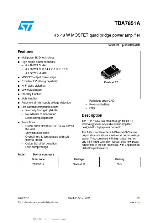
TDA7851A, 规格书,Datasheet 资料
Block diagram . . . . . . . . . . . . . . . . . . . . . . . . . . . . . . . . . . . . . . . . . . . . . . . . . . . . . . . . . . . . 5
Application circuit . . . . . . . . . . . . . . . . . . . . . . . . . . . . . . . . . . . . . . . . . . . . . . . . . . . . . . . . . 5
– Fortuitous open GND – Reversed battery – ESD
Description
The TDA7851A is a breakthrough MOSFET technology class AB audio power amplifier, designed for high-power car radio. The fully complementary P-Channel/N-Channel output structure allows a rail-to-rail output voltage swing. This, combined with high output current and minimized saturation losses, sets new power references in the car-radio field, with unparalleled distortion performance.
TDA7851A
List of tables
List of tables
TDA2052V,TDA2052H, 规格书,Datasheet 资料
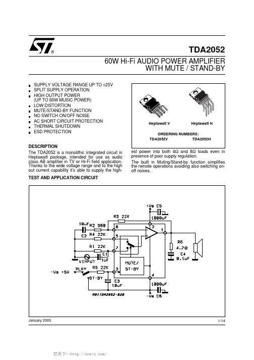
TDA205260W Hi-Fi AUDIO POWER AMPLIFIERWITH MUTE / STAND-BYSUPPLY VOLTAGE RANGE UP TO ±25V SPLIT SUPPLY OPERATION HIGH OUTPUT POWER(UP TO 60W MUSIC POWER)LOW DISTORTIONMUTE/STAND-BY FUNCTION NO SWITCH ON/OFF NOISEAC SHORT CIRCUIT PROTECTION THERMAL SHUTDOWN ESD PROTECTIONDESCRIPTIONThe TDA2052 is a monolithic integrated circuit in Heptawatt package, intended for use as audio class AB amplifier in TV or Hi-Fi field application.Thanks to the wide voltage range and to the high out current capability it’s able to supply the high-est power into both 4Ω and 8Ω loads even in presence of poor supply regulation.The built in Muting/Stand-by function simplifies the remote operations avoiding also switching on-off noises.This is advanced information on a new product now in development or undergoing evaluation. Details are subject to change without notice.January 2003®Heptawatt V Heptawatt H ORDERING NUMBERS:TDA2052V TDA2052HTEST AND APPLICATION CIRCUIT1/14ABSOLUTE MAXIMUM RATINGSSymbol ParameterValue Unit V S DC Supply Voltage±25V I O Output Peak Current (internally limited)6A P tot Power Dissipation T case = 70°C 30W T op Operating Temperature Range 0 to +70°C T stg , T jStorage and Junction Temperature-40 to +150°CBLOCK DIAGRAM1234567NON INVERTING INPUT(PLAY)INVERTING INPUT-V SSTAND-BY/MUTE +V S OUTPUTD95AU326tab connected to pin 4NON INVERTING INPUT(MUTE)PIN CONNECTION (Top view)ELECTRICAL CHARACTERISTICS (Refer to the test circuit, G V = 32dB; V S + 18V; f = 1KHz; T amb =25°C, unless otherwise specified.)Symbol ParameterTest ConditionMin.Typ.Max.Unit V S Supply Range+6+25V I q Total Quiescent Current V S = +22V204070mA I b Input Bias Current +0.5µA V OS Input Offset Voltage +15mV I OS Input Offset Current +200nA P O Music Output Power IEC268-3 Rules (*)V S = + 22.5, R L = 4Ω, d = 10%, t = 1s 5060W P OOutput Power (continuous RMS)d = 10%RL = 4ΩR L = 8ΩV S = +22V, R L = 8Ω3530402233W W W d = 1%R L = 4ΩR L = 8ΩV S = +22V, R L = 8Ω321728W W WdTotal Harmonic DistortionR L = 4ΩP O = 0.1 to 20W; f = 100Hz to 15KHz V S + 22V, R L = 8ΩP O = 0.1 to 20W; f = 100Hz to 15KHz0.10.10.70.5%%SR Slew Rate35V/µs G V Open Loop Voltage Gain 80dBe N Total Input Noise A Curvef = 20Hz to 20KHz2310µV µV R i Input Resistance 500K ΩSVR Supply Voltage Rejection f = 100Hz, V ripple = 1V RMS 4050dB T SThermal Shutdown145°CMUTE/STAND-BY FUNCTION (Ref. –V S )VT ST-BY Stand-by - Threshold11.8V VT PLAY Play Threshold2.74V I q ST-BY Quiescent Current @ Stand-by V pin 3 = 0.5V13mA ATT ST-BYStand-by Attenuation 7090dB I pin3Pin 3 Current @ Stand-by–1+10µANote (*):MUSIC POWER CONCEPTMUSIC POWER is ( according to the IEC clauses n.268-3 of Jan 83) the maximal power which the amplifier is capable of producing across the rated load resistance (regardless of non linearity) 1 sec after the application of a sinusoidal input signal of frequency 1KHz.According to this definition our method of measurement comprises the following steps:1) Set the voltage supply at the maximum operating value -10%2) Apply a input signal in the form of a 1KHz tone burst of 1 sec duration; the repetition period of the signal pulses is > 60 sec 3) The output voltage is measured 1 sec from the start of the pulse 4) Increase the input voltage until the output signal show a THD = 10%5) The music power is then V 2out /R1, where V out is the output voltage measured in the condition of point 4) and R1 is the rated load impedance The target of this method is to avoid excessive dissipation in the amplifier.THERMAL DATASymbol DescriptionValue Unit R th j-caseThermal Resistance Junction-caseMax2.5°C/WAPPLICATIONS SUGGESTIONS (See Test and Application Circuit)The recommended values of the external components are those shown on the application circuit. Differ-ent values can be used; the following table can help the designer.Comp.Value PurposeLarger Than Smaller Than R122K Ω (*)Input Impedance Increase of Input Impedance Decrease of Input Impedance R2560ΩClosed Loop Gain set to 32dB (**)Decrease of Gain Increase of Gain R322K Ω (*)Increase of GainDecrease of GainR422K Ω (*)Input Impedance @ Mute R522K Ω Stand-by Time Constant R6 4.7ΩFrequency Stability Danger of oscillationsDanger of oscillations C11µF Input DC Decoupling Higher Low-frequency cut-offC210µF Feedback DC Decoupling Higher Low-frequency cut-offC310µF Stand-by Time Constant C40.100µF Frequency Stability Danger of OscillationsC5, C61000µFSupply Voltage Bypass(*) R1 = R3 = R4 for POP optimization (**) Closed Loop Gain has to be ≥30dBFigure 1:Output Power vs. Supply VoltageFigure 2: Distortion vs. Output PowerTYPICAL CHARACTERISTICSFigure 3: Output Power vs. Supply Voltage.Figure 4: Distortion vs. Output Power.Figure 5: Distortion vs. Frequency.Figure 6: Distortion vs. Frequency.Figure 7: Quiescent Current vs. Supply Voltage Figure 8: Supply Voltage Rejection vs. Frequency.Figure 9: Bandwidth.Figure 10: Output Attenuation & Quiescent Cur-rent vs. V pin3.Figure 11: Total Power Dissipation & Efficiency vs. Output Power.Figure 12: Total Power Dissipation & Efficiency vs. Output Power.Figure 13: P.C. Board and Components Layout of the Circuit of Fig. 14 (1:1 scale)Figure 14: Demo Board Schematic.MUTE/STAND-BY FUNCTIONThe pin 3 (MUTE/STAND-BY) controls the ampli-fier status by three different thresholds, referred to -V S.When its voltage is lower than the first threshold (1V, with a +70mV hysteresis), the amplifier is in STAND-BY and all the final stage current gener-ators are off. Only the input MUTE stage is on in order to prevent pop-on problems.At V pin3=1.8V the final stage current generators are switched on and the amplifier operates in MUTE.For V pin3 =2.7V the amplifier is definitely on(PLAY condition)Figure 15.SHORT-CIRCUIT PROTECTIONThe TDA 2052 has an original circuit which pro-tects the device during accidental short-circuit be-tween output and GND / -Vs / +Vs, taking it in STAND-BY mode, so limiting also dangerous DC current flowing throught the loudspeaker.If a short-circuit or an overload dangerous for the final transistors are detected, the concerned SOA circuit sends out a signal to the latching circuit (with a 10µs delay time that prevents fast random spikes from inadvertently shutting the amplifier off) which makes Q1 and Q2 saturate (see Block Diagram). Q1 immediately short-circuits to ground the A point turning the final stage off while Q2 short-circuits to ground the external capacitor driving the pin 3 (Mute/Stand-by) towards zero potential.Only when the pin 3 voltage becomes lower than 1V, the latching circuit is allowed to reset itself and restart the amplifier, provided that the short-circuit condition has been removed. In fact, a win-dow comparator is present at the output and it is aimed at preventing the amplifier from restarting if the output voltage is lower than 0.35 Total Supply Voltage or higher than 0.65 Total Supply Voltage. If the output voltage lies between these two thresholds, one may reasonably suppose the short-circuit has been removed and the amplifier may start operating again.The PLAY/MUTE/STAND-BY function pin (pin 3) is both ground- and positive supply-compatible and can be interfaced by means of the R5, C3 net either to a TTL or CMOS output (µ-Processor) or to a specific application circuit.The R5, C3 net is fundamental, because connect-ing this pin directly to a low output impedance driver such as TTL gate would prevent the correct operation during a short-circuit. Actually a final stage overload turns on the protection latching circuit that makes Q2 try to drive the pin 3 voltage under 0.8 V. Since the maximum current this pin can stand is 3 mA, one must make sure the fol-lowing condition is met:R5≥(V A− 0.7V)3mAthat yields: R5, min = 1.5 KΩ with V A=5V.In order to prevent pop-on and -off transients, it is advisable to calculate the C3, R5 net in such a way that the STAND-BY/MUTE and MUTE/PLAY threshold crossing slope (positive at the turn-onand vice-versa) is less than 100 V/sec.Figure 16: Thermal Protection Block Diagram THERMAL PROTECTIONThe thermal protection operates on the 125µA current generator, linearly decreasing its value from 90°C on. By doing this, the A voltage slowly decreases thus switching the amplifier first to MUTE (at 145°C) and then to STAND-BY (155°C).Figure 17: Maximum Allowable Power Dissipa-tion vs. Ambient Temperature.The maximum allowable power dissipation de-pends on the size of the external heatsink (ther-mal resistance case-ambient); figure 17 shows the dissipable power as a function of ambient temperature for different thermal resistance.Figure 18: Multiway Application CircuitAPPLICATION NOTES90W MULTIWAY SPEAKER SYSTEMThe schematic diagram of figure 18, shows the solution that we have closen as a suggestion for Hi-Fi and especially TV applications.The multiway system provides the separation of the musical signal not only for the loudspeakers,but also for the power amplifiers with the following advantages:- reduced power level required of each individ-ual amplifier- complete separation of the ways (if an ampli-fier is affected by clipping distortion, the oth-ers are not)- protection of tweeters (the high power har-monics generated by low frequency clipping can not damage the delicate tweeters that are driven by independent power amplifier)- high power dedicated to low frequenciesFigure 21:Distortion vs Output Power(Midrange/Tweeter)Figure 20: Distortion vs Output Power(Subwoofer)Figure 19: Frequency ResponseAs shown in Figure 19, the R-C passive network for low-pass and High-pass give a cut with a slope of 12dB/octaveA further advantage of this application is that con-necting each speaker direcly to its amplifier, the musical signal is not modified by the variations of the impedance of the crossover over frequency.The subwoofer is designed for obtaining high sound pressure level with low distortion without stereo effect.In the application of figure 18, the subwoofer plays the 20 to 300 Hz frequency range, while the remaining 300 Hz to 20KHz are sent to two sepa-rate channels with stereo effect.The multiway system makes use of three TDA2052, one for driving the subwoofer with P OUT higher than 40W (THD = 10%), 28W undis-torted (THD = 0.01%), while the others two TDA2052 are used for driving the mid/high fre-quency speakers of L/R channels, delivering P OUT = 25W (THD = 10%) and 20W @ THD =0.01%Weight: 1.90grHeptawatt VDIM.mm inch MIN.TYP.MAX.MIN.TYP.MAX.A 4.80.189C 1.370.054D 2.4 2.80.0940.110D1 1.2 1.350.0470.053E 0.350.550.0140.022E10.70.970.0280.038F 0.60.80.0240.031G 2.34 2.54 2.740.0950.1000.105G1 4.88 5.08 5.280.1930.2000.205G27.427.627.820.2950.3000.307H210.40.409H310.0510.40.3960.409L 16.716.917.10.6570.6680.673L114.920.587L221.2421.5421.840.3860.8480.860L322.2722.5222.770.8770.8910.896L4 1.290.051L5 2.6 2.830.1020.1100.118L615.115.515.80.5940.6100.622L76 6.35 6.60.2360.2500.260L90.20.008L10 2.1 2.70.0820.106L11 4.3 4.80.1690.190M 2.55 2.8 3.050.1000.1100.120M1 4.83 5.085.330.1900.2000.210V440 (typ.)Dia3.653.850.1440.152ALL1CD1L5L2L3DEM1MH3Dia.L7L11L10L6H2FG G1G2E1FE L9V4L4H2HEPTAMEC0016069OUTLINE AND MECHANICAL DATAOUTLINE AND MECHANICAL DATAL2L3EDV5CAFL7L6L4H2FL5L10L11H3HEPTHMEC.EPSDia.L1L9G G1G2H2D1E1FEResin betweenleadsDIM.mminch MIN.TYP .MAX.MIN.TYP .MAX.A 4.800.188C 1.370.054D 2.40 2.800.0940.11D1 1.20 1.350.0470.053E 0.350.550.0140.022E10.700.970.030.036F 0.600.800.0240.031G 2.34 2.54 2.740.0920.10.108G1 4.88 5.08 5.280.1920.20.208G27.427.627.80.2920.30.307H210.400.41H310.0510.400.3950.409L1 3.90 4.20 4.500.1530.1650.177L218.1018.4018.700.7120.7240.736L3 4.88 5.08 5.280.1920.20.208L4 1.290.05L5 2.60 3.000.1020.118L615.1015.800.5940.622L7 6.00 6.600.2360.260L9 3.9 4.2 4.50.1530.1650.177L10 2.10 2.700.0830.106L13 4.30 4.800.1690.189V589˚(Min.),90˚(Typ.),91˚(Max.)DIA3.653.850.1430.151Heptawatt H0080180Information furnished is believed to be accurate and reliable. However, STMicroelectronics assumes no responsibility for the consequences of use of such information nor for any infringement of patents or other rights of third parties which may result from its use. No license is granted by implication or otherwise under any patent or patent rights of STMicroelectronics. Specification mentioned in this publication are subject to change without notice. This publication supersedes and replaces all information previously supplied. STMicroelectronics products are not authorized for use as critical components in life support devices or systems without express written approval of STMicroelectronics.The ST logo is a registered trademark of STMicroelectronics© 2003 STMicroelectronics – Printed in Italy – All Rights ReservedSTMicroelectronics GROUP OF COMPANIESAustralia - Brazil - Canada - China - Finland - France - Germany - Hong Kong - India - Israel - Italy - Japan - Malaysia - Malta - Morocco -Singapore - Spain - Sweden - Switzerland - United Kingdom - United States.。
TDA集成块引脚功能
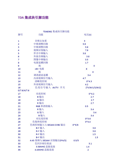
TDA集成块引脚功能TDA8362集成块引脚功能脚号功能电压(v)1 音频去加重 32 中频调整回路 5.93 中频调整回路 5.94 视频识别输入7.95 伴音中频输入 3.86 外接音频输入 3.87 图像中频输出 3.58 电源退耦回路 1.79 地010 +8V电源811 地012 调谐滤波退耦 3.413 内部视频信号输入 4.714 清晰度控制0~4.315 外部视频信号输入 4.216 色度信号输入AV/TV开关(TV/AV1/S/AV2) 0/7.6/4/7.617 亮度控制0~4.218 B输出 2.719 G输出 2.720 R输出 2.721 RGB和消隐输入0.522 R输入 3.423 G输入 3.424 B输入 3.425 对比度控制0~3.626 色饱和度控制0~4.427 色相控制输入与SECAM.CVBS输出0~5/628 B-Y输入 3.829 R-Y输入 3.830 R-Y输出 1.531 B-Y输出 1.532 4.43基频与SECAM识别输出(P.N/S) 0.5/533 色同步相位检波 5.134 3.58MHZ晶振连接 1.435 4.43MHZ晶振连接 236 行起振电源8.437 行激励输出0.538 行逆程入\沙堡脉冲出 2.839 行中心调整与滤波 2.840 行相位滤波回路 3.941 场逆程输入 2.442 场起振2.743 场激励输出 144 AFC输出 4.745 中频输入4.146 中频输入 4.147 高频头AGC输出8.848 AGC检波 3.849 RF AGC调节 1.350 音频输出 3.351 伴音解调退耦 4.152 电源退耦6.5TDA3862的亮度信号是由IC的7脚输出全电视信号,经IC的7脚上的三极管发射极输出经三极管缓冲由发射极输出经4.5MHz、5.5MHz、6.0MHz、6.5MHz 信号陷波分别送入集成电路4053的12脚和13脚,利用其内部的开关进行制式转换。
TDA系列
TDA2030 14W Hi-Fi 音频放大器TDA7000T FM 单片调频接收电路TDA7010T FM 单片调频接收电路TDA7021T FM MTS 单片调频接收电路TDA7040T 低电压锁相环立体声解码器TDA7050 低电压单/双声道功率放大器TDA1521 2×12W Hi-Fi 音频功率放大器TDA1010 音频功率放大集成电路TDA1013 音频功率放大集成电路TDA1037 音频功率放大集成电路TDA1170N 场扫描输出集成电路TDA1175P 场扫描输出集成电路TDA1180P 行扫描信号处理集成电路TDA120P 电子开关切换集成电路TDA1220 调频/调幅中频放大集成电路TDA1300T 射频放大集成电路TDA1301 伺服处理集成电路TDA1306 数/模转换集成电路TDA1311T 存储集成电路TDA1512Q 音频功率放大集成电路TDA1515 音频功率放大2W×2集成电路TDA1516Q 音频功率放大集成电路TDA1521A 双声道音频功率放大集成电路TDA1522 双声道音频功率放大20W×2集成电路TDA1524 立体声音量、音调控制集成电路TDA1526 双声道音量、音调控制集成电路TDA1541A 数/模转换集成电路TDA1542 有源滤波集成电路TDA1543A 数/模转换集成电路TDA1602A 单片录、放音集成电路TDA1675 场扫描输出集成电路TDA16846 开关电源稳压集成电路TDA1771 场扫描输出集成电路TDA1905 音频功率放大集成电路TDA1950 同步信号分离集成电路TDA2004 双声道音频功率放大集成电路TDA2005M 音频功率放大集成电路TDA2006H 音频功率放大集成电路TDA2007 双声道音频功率放大6W×2集成电路TDA2009 双声道音频功率放大集成电路TDA2030 音频功率放大集成电路TDA2030A 音频功率放大集成电路TDA2040A 音频功率放大集成电路TDA2151 色度、亮度信号放大集成电路TDA2170 场扫描输出集成电路TDA2270 场扫描输出集成电路TDA2320 红外遥控信号接收集成电路TDA2460C2 音频信号处理集成电路TDA2461C1 伴音中频放大及鉴频集成电路TDA2523 色同步解码、自动色度控制集成电路TDA2530 矩阵集成电路TDA2540Q 中频放大、视频检波集成电路TDA2541 图像中频放大集成电路TDA2545A 图像中频放大集成电路TDA2549 中频放大、检波集成电路TDA2556 伴音中频放大、鉴频集成电路TDA2560 亮度信号放大、色饱和度控制集成电路TDA2571AQ 行、场扫描信号处理集成电路TDA2577A 行、场扫描信号处理集成电路TDA2579 行、场扫描信号处理集成电路TDA2581Q 电源厚膜集成电路TDA2590Q 行扫描信号处理集成电路TDA2595 行、场扫描信号处理集成电路TDA2611A 音频功率放大5W集成电路TDA2613 音频功率放大集成电路TDA2616 双声道音频功率放大12W集成电路TDA2640 开关电源稳压集成电路TDA2653A 场扫描输出集成电路TDA2655B 场扫描输出集成电路TDA2822 双声道音频功率放大集成电路TDA3047 红外遥控信号接收集成电路TDA3190 伴音中频放大、鉴频及功率放大集成电路TDA3301B 色度解码集成电路TDA3504 视频解码集成电路TDA3505 视频信号控制集成电路TDA3540Q 中频放大、视频检波集成电路TDA3561 色度解码集成电路TDA3562A 色度解码集成电路TDA3565 色度解码集成电路TDA3592A 制式转换集成电路TDA3654 场扫描输出集成电路TDA3803A 立体声解码集成电路TDA3810 混响立体声处理集成电路TDA3857 伴音处理集成电路TDA4193 色度解码集成电路TDA4410 图像中频放大集成电路TDA4420 中频信号处理集成电路TDA4433 电视信号识别处理集成电路TDA4440 中频信号处理集成电路TDA4443 图像中频信号处理集成电路TDA4501 电视信号处理集成电路TDA4502A 电视信号处理集成电路TDA4505 电视信号处理集成电路TDA4505E 中频、鉴频、行场扫描信号处理集成电路TDA4510 色度解码集成电路TDA4555 色度解码集成电路TDA4565 色度瞬态特性改善集成电路TDA4566 缓冲放大集成电路TDA4580 视频接口集成电路TDA4601 开关电源稳压集成电路TDA4605-2 场效应管驱动电源集成电路TDA4605-3 开关电源控制集成电路TDA4650 色度解码集成电路TDA4660 延迟集成电路TDA4661 延迟集成电路TDA4663 基带延迟集成电路TDA4670 图像信号处理集成电路TDA4671 色度瞬态特性改善集成电路TDA4681 矩阵变换及亮度控制集成电路TDA4685 视频控制集成电路TDA4686 色差矩阵视频处理集成电路TDA4688 色差矩阵视频处理集成电路TDA4780 视频信号处理集成电路TDA4800 场扫描输出集成电路TDA4821P 行、场幅度自动控制集成电路TDA4850 多频彩显行场扫描控制集成电路TDA4852 行、场偏转信号处理集成电路TDA4854 总线控制同步偏转信号处理集成电路TDA4855 彩显自动同步扫描信号处理集成电路TDA4860 场扫描输出集成电路TDA4863AJ 场扫描输出集成电路TDA4863J 场扫描输出集成电路TDA4866 场扫描全桥电流驱动输出集成电路TDA4881 视频信号控制集成电路TDA4885 总线控制彩显视频信号处理150MHz集成电路TDA4886 总线控制视频信号处理140MHz集成电路TDA4918 开关电源控制集成电路TDA4950 枕形校正集成电路TDA5330T 电视调谐集成电路TDA5637 电视调谐集成电路TDA5700 调幅/调频收音集成电路TDA5731M 低压全频道调谐集成电路TDA5736M 电视调谐集成电路TDA6101Q 视频输出放大集成电路TDA6103Q 视频输出放大集成电路TDA6107Q 视频输出放大集成电路TDA6108 视频输出放大集成电路TDA6111Q 视频输出放大集成电路TDA6120Q 视频输出放大集成电路TDA6151 视频处理集成电路TDA7010T 调频收音集成电路TDA7021T 单片调频收音集成电路TDA7050 双声道音频功率放大集成电路TDA7053A 双声道音频功率放大集成电路TDA7056B 音频放大集成电路TDA7057AQ 双声道音频功率放大集成电路TDA7073 电机驱动集成电路TDA7253 音频功率放大集成电路TDA7263M 双声道音频功率放大集成电路TDA7265 双声道音频功率放大集成电路TDA7273 单片放音集成电路TDA7347P 电子开关切换集成电路TDA7429S 立体声音频处理集成电路TDA7438B 调谐控制集成电路TDA7449 音频调整集成电路TDA7494 音频功率放大集成电路TDA7495 音频功率放大集成电路TDA7496 双声道音频功率放大集成电路TDA7496L 音频功率放大集成电路TDA8132 电源稳压输出5V/12V集成电路TDA8133 复位电源稳压输出十5V/8V集成电路TDA8135 电源稳压输出+5V集成电路TDA8137 复位电源稳压5V×2集成电路TDA8138 电源取样检测控制集成电路TDA8139 电源稳压复位集成电路TDA8143 行扫描激励集成电路TDA8145 光栅东-西校正集成电路TDA8172 场扫描输出集成电路TDA8173 场扫描输出集成电路TDA8174 场扫描输出集成电路TDA8177F 场扫描输出集成电路TDA8190 伴音中放、鉴频及音频功率放大集成电路TDA8204 丽音解码集成电路TDA8305 图像、伴音、扫描信号处理集成电路TDA8310 画中画色度信号处理集成电路TDA8341 中频信号处理集成电路TDA8350Q 场扫描输出集成电路TDA8351 场扫描输出集成电路TDA8351A 场扫描输出集成电路TDA8354 场扫描输出集成电路TDA8356 场扫描输出集成电路TDA8362 视频、色度、中频行场扫描小信号处理集成电路TDA8366 电视信号处理集成电路TDA8366N3D 色度、亮度、行场扫描信号处理集成电路TDA8375 电视信号处理集成电路TDA8376 色度、亮度及行场扫描处理集成电路TDA8380 开关电源控制集成电路TDA8395 色度解码集成电路TDA8395T 色度处理集成电路TDA8417 总线控制立体声集成电路TDA8420 总线控制立体声处理集成电路TDA8424 总线控制双声道伴音信号处理集成电路TDA8425 总线控制立体声音频处理集成电路TDA8440 电视信号切换集成电路TDA8442 色度、亮度信号控制集成电路TDA8443A 总线控制视频接口集成电路TDA8443B 矩阵变换集成电路TDA8444 总线控制数/模转换集成电路TDA8461 色度解码集成电路TDA8540 视频交换矩阵集成电路TDA8563Q 双声道音频功率放大集成电路TDA8601 基色消隐切换开关集成电路TDA8732 丽音解调集成电路TDA8747N 音频/视频切换集成电路TDA8808 光电信号处理集成电路TDA8808T 光电信号处理集成电路TDA8809 误差信号处理集成电路TDA8822 音调控制集成电路TDA8841 电视信号处理集成电路TDA8843 电视信号处理集成电路TDA8944J 音频放大集成电路TDA8945J 音频功率放大集成电路TDA9045 视频信号选择集成电路TDA9102 偏转信号处理集成电路TDA9103 多频彩显偏转信号处理集成电路TDA9105 多频彩显偏转信号处理集成电路TDA9106 多频彩显偏转信号处理集成电路TDA9109 总线控制自动同步扫描信号处理集成电路TDA9110 总线控制多频彩显偏转信号处理集成电路TDA9111 扫描信号处理集成电路TDA9112 总线控制多频彩显偏转信号处理集成电路TDA9115 总线控制多频彩显偏转信号处理集成电路TDA9141 解码、同步处理集成电路TDA9143 解码、同步处理集成电路TDA9151B 可编程扫描控制集成电路TDA9160A 子画面信号处理集成电路TDA9170 色度、亮度信号校正处理集成电路TDA9177 色度、亮度信号瞬态校正处理集成电路TDA9178 视频信号处理集成电路TDA9181 梳状滤波集成电路TDA9203A 总线控制视频信号处理70MHz集成电路TDA9206A 视频信号处理130MHz集成电路TDA9207 总线控制视频信号处理150MHz集成电路TDA9321H 总线控制电视信号处理集成电路TDA9332H 总线控制电视光栅处理集成电路TDA9380 单片电视信号处理集成电路TDA9383 单片电视信号处理集成电路TDA9429S 音频信号切换及处理集成电路TDA9511 视频输出放大集成电路TDA9535 视频输出放大集成电路TDA9800 视调谐集成电路TDA9801 中频锁相环解调、鉴频集成电路TDA9808 中频信号处理集成电路TDA9815 中频信号处理集成电路TDA9820 双通道电视内载波丽音解调集成电路TDA9859 总线控制、高保真音频信号处理集成电路TDA9874A 数字伴音解调、解码集成电路TDA9875A 数字电视伴音处理集成电路。
TDA技术
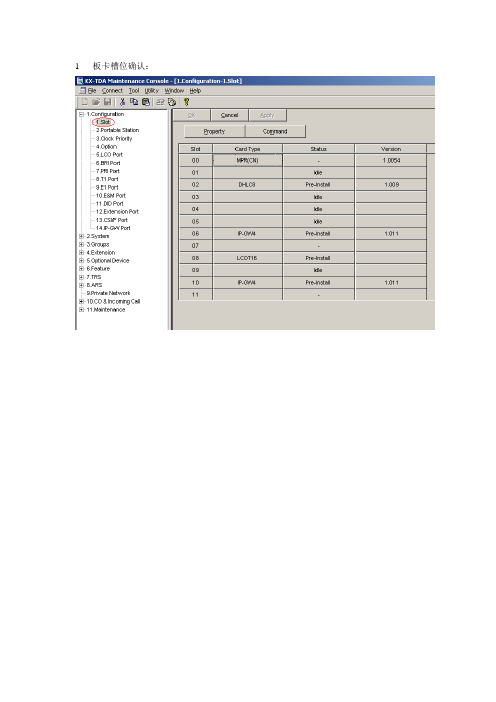
1板卡槽位确认:2分机号码更改:2.1分机字头分配2.2分机号码修改3服务等级编程:3.1长途限制等级设定3.2服务等级对应长途限制等级设定4.1外线响铃分机设定:5.1呼入组浮动号码及组类型设置5.2呼入组成员设置5.3DIL设置:6ARS设置:6.1ARS开启模式设置:6.2 2.ARS引导数字设置:6.3ARS前置数字设置:7计费码插入长途限制:7.1计费开启模式设置:7.2验证码:7.3分机密码1.移动COS,输入方法1(使用分机密码打):*47*+分机号码+分机密码+9+外线号码2.随身密码,输入方法2(使用验证码打):*47*+验证码+9+外线号码TDA200查询已拨电话:2-9 打开redial call log.TDA100 3.0版本改日夜服务的时间,要自动转换:2-4设置时间,选择automatic就是自动切换。
TDA日夜切换的代码TDA200总机怎么调日夜服务?*7800白天/*7801夜晚/*7802午餐/*7803休息TDA200 76话机铃声更改:PROG+CO键两次.TDA100打开分机呼叫等待:*7311分机呼叫等待打开.TDA200设了三个分机作UCD组,都占线怎么转到别的话机?3-5-1第二张表设溢出.TDA200点亮留言灯?*701+分机号码.TDA100话机的摘机热线时间在哪里设的?2-3第一张表.TDA200会议的证实音在哪里取消?2-9的第三张表.TDA200分机打分机要等到3声后对端分机才振铃?2-3 inter digit。
TDA200无应答转移的时间?*713+时间TDA200 PRI做外线需要设置什么?关闭CRC4模式,打开ringbTDA200总机的玲声能不能区分内线和外线呼叫?可以,PROGRAM+两次INTERCOM/CO键+选择铃音+STOREack tone.TDA100 PRI 送忙音怎么做?1-7笫6张表CCBS改为ON.松下TDA100组全忙溢出到外线的测试1.TDA100主机一台,普通话机二部,数字话机两部。
TDA8925资料
BOOT1
EN1 SW1 REL1 STAB DIAG POWERUP
OUT1
BOOT2
EN2 SW2 REL2
14 17 16 CONTROL AND HANDSHAKE
OUT2
VSS1 VSS2
Fig.1 Block diagram.
2004 May 06
Hale Waihona Puke 4Philips Semiconductors
Product specification
Power stage 2 x 15 to 25 W class-D audio amplifier
7 PINNING SYMBOL SW1 REL1 DIAG PIN 1 2 3 DESCRIPTION digital switch input; channel 1 digital control output; channel 1 digital open-drain output for overtemperature and overcurrent report digital enable input; channel 1 positive power supply; channel 1 bootstrap capacitor; channel 1 PWM output; channel 1 negative power supply; channel 1 decoupling internal stabilizer for logic supply negative power supply; channel 2 PWM output; channel 2 bootstrap capacitor; channel 2 positive power supply; channel 2 digital enable input; channel 2 enable input for switching on internal reference sources digital control output; channel 2 digital switch input; channel 2
TDA7490L, 规格书,Datasheet 资料
1/11TDA7490LDecember 20051FEATURES■20W + 20W OUTPUT POWER: @R L = 8Ω/4Ω; THD = 10%■HIGH EFFICIENCY■WIDE SUPPLY VOLTAGE RANGE (FROM ±10 TO ±25V)■SPLIT SUPPLY, SINGLE SUPPLY OPERATION■TURN OFF/ON POP FREE ■ST-BY AND MUTE FEATURES■SHORT CIRCUIT PROTECTION ACROSS THE LOAD■THERMAL OVERLOAD PROTECTION ■EXTERNALLY SINCHRONIZABLE ■BRIDGE CONFIGURATION2DESCRIPTIONThe TDA7490L is a dual audio class D amplifier assembled in Flexiwatt 25 package; it is specially designed for high efficiency application mainly for TV and Home Stereo sets.20W + 20W STEREO CLASS-D AMPLIFIER40W MONO IN BTLFigure 2. Test and Application Circuit. (Stereo Configuration)Rev. 2Figure 1. PackageTable 1. Order CodesPart Number Package TDA7490LFlexiwatt 25t eP r od u c t (s)Ob so l e t ePr od u c t (s )- O bs ol TDA7490L2/11Figure 3. Test and Application Circuit. (Bridge Configuration)Table 2. Absolute Maximum RatingsTable 3. Thermal DataSymbol ParameterValue Unit V CC DC Supply Voltage (no signal)±30V P tot Power Dissipation T case = 70°C35W T stg , T j Storage and Junction T emperature –40 to 150°C T op Operating T emperature Range0 to 70°C V 6,8,10,18Maximum Voltage on pins # 6,8,10,18 referred to GND±5VSymbolParameterValue Unit R th j-caseThermal Resistance Junction-caseTyp.1°C/WOb so l e t ePr od u3/11TDA7490LFigure 4. Application in Supply VoltageOb sol e t ePr od u c t (s ) -O bs o l e t eP r odTDA7490L4/11Figure 5. Pin ConnectionTable 4. Pin DescriptionPin N°Name Function1-V CC sign/sub Negative signal/substrate supply 2-V CCpow1Negative power supply CH13out 1PWM output of CH14+V CCpow1Positive power supply CH15BOOT1Bootstrap CH16STBY -MUTE Control State Pin7FEED1Feedback pin 1 CH18OSC Master Oscillator Setting Freequency Pin (or external sync.)9FEED2Feedback pin2 CH110IN1Input CH111T1T riangular waveform CH112+5V+5V regulator (only for internal purposes)13GNDSignal ground 14CURREF Setting current resistor 15T2T riangular waveform CH216-5V -5V regulator (only for internal purposes)17FEED3Feedback pin1 CH218IN2Input CH219FEED4Feedback pin2 CH220NC Not connected 21BOOT2Bootstrap CH222+V CCpow2Positive power supply CH223OUT2PWM output of CH224-V CCpow2Negative power supply CH225V reg10V regulatorOb so l e t ePr od u c t (s ) -O bs o l e t eP r od u c t(s) 5/11TDA7490L*: Po = measured across the load using the following inductor: COIL58120 MPPA 2 (magnectics) TURNS= 20∅ 1 mm (1) L = 15µH, C = 470nF(3) ∆Gv is intended with R2, R17, R5, R9 1% precision (4) Fsw = 0.25 · (1/(300ns + R13 · (C17 + 76pF) . 0.85)(5) V RMAX = (+Vcc) - (-Vcc) when V R ≥V RMAX the device goes in Stand-By modeTable 5. Electrical Characteristics(Refer to the test circuit, V CC = ±19V; R L = 8Ω; Demod. filter L = 30µH, C = 220nF; f = 1KHz; f sw = 200kHz;T amb = 25°C unless otherwise specified.)Symbol ParameterTest ConditionMin. Typ.Max.Unit V S Supply Range±10±25V I q T otal Quiescent Current R L = ∞ no LC filter70120mA V OS Output Offset Voltage -150+150mV P o Output PowerTHD = 10%THD= 1%2016W W P o(BTL)Output Power in Bridge ConfigurationV S = ±20V ; R L = 16ΩTHD = 10%THD=1%4032W W V S =±15.5V; R L = 8ΩTHD = 10%THD=1%4032W WP o (1)Output PowerR L = 4Ω Vcc=±13.5V THD = 10%THD=1%1814.5W W P D Maximum Dissipated Power V CC = ±19V; R L = 8ΩP ο = 20W + 20W; THD = 10% 5.6W ηEfficiency (')P o = 20W + 20W 86%THD T otal Harmonic Distortion R L = 8Ω; Po = 1 W 0.1%I max Overcurrent Protection ThresholdR L = 05A T j Thermal Shut-down Junction T emperature 150°CG v Closed Loop Gain 293031dB ∆G v (3)Gain Matching -1+1dB e N T otal Input Noise R G = 50Ω A Curvef = 20Hz to 22KHz712µV µV C T Cross talk f = 1 KHz, P o = 1W55dB R i Input Resistance2030k ΩSVR Supply Voltage Rejection f = 100Hz; V r = 0.560dBV rmax Overvoltage Threshold (5)5560V T r , T t Rising and Falling Time5070ns R DSON Power T ransistor on Resistance 0.40.8ΩFsw (4)Switching Frequency Range100200230KHzMUTE & STAND-BY FUNCTIONS V ST-BY Stand-by range 00 7V V MUTE Mute Range 1.7 2.5V V PLAY Play Range 45V A MUTE Mute Attenuation5560dB I qST-BYQuiescent Current @ Stand-by35mAOb so l e t ePr od u c t (s ) -O bs o l e t eP r od u c t (s) TDA7490L6/11Figure 6. P.C. Board and Component Layout of the Figs. 2, 3 (for Stereo and Bridge CompatibleConfiguration)Component SideSolderSide)7/11TDA7490L Figure 7. Distortion vs. Output PowerFigure 8. Distortion vs. Output PowerFigure 9. Crosstalk vs. FrequencyFigure 10. Frequency ResponseFigure 11. Power Dissipation vs. Output PowerFigure 12. Distortion vs. Output Power in BTLO b s ol e te Pr o du ct(s)-O bs ol e te Pr o du ct(sTDA7490L8/11Figure 13. Distortion vs. Output Power in BTL Figure 14. Pout vs Supply VoltageTDA7490L Figure 15. Flexiwatt 25 Mechanical Data & Package Dimensions9/11Ob so l e t ePr od u c t (s ) -O bs o l e t eP r od u c t (s) TDA7490L10/11Table 6. Revision HistoryDate RevisionDescription of ChangesMarch 20011First IssueDecember 20052Corrected the value of the inductance in the caption of the T able 5 “Electrical Characteristics”.O b s ol e te Pr o du ct(s)-O bs ol e te Pr o du ct(s)Information furnished is believed to be accurate and reliable. However, STMicroelectronics assumes no responsibility for the consequences of use of such information nor for any infringement of patents or other rights of third parties which may result from its use. No license is granted by implication or otherwise under any patent or patent rights of STMicroelectronics. Specifications mentioned in this publication are subject to change without notice. This publication supersedes and replaces all information previously supplied. STMicroelectronics products are not authorized for use as critical components in life support devices or systems without express written approval of STMicroelectronics.The ST logo is a registered trademark of STMicroelectronics.All other names are the property of their respective owners© 2005 STMicroelectronics - All rights reservedSTMicroelectronics group of companiesAustralia - Belgium - Brazil - Canada - China - Czech Republic - Finland - France - Germany - Hong Kong - India - Israel - Italy - Japan - Malaysia - Malta - Morocco - Singapore - Spain - Sweden - Switzerland - United Kingdom - United States of America11/11TDA7490L 芯天下--/。
TDA系列
TDA2030 14W Hi-Fi 音频放大器TDA7000T FM 单片调频接收电路TDA7010T FM 单片调频接收电路TDA7021T FM MTS 单片调频接收电路TDA7040T 低电压锁相环立体声解码器TDA7050 低电压单/双声道功率放大器TDA1521 2×12W Hi-Fi 音频功率放大器TDA1010 音频功率放大集成电路TDA1013 音频功率放大集成电路TDA1037 音频功率放大集成电路TDA1170N 场扫描输出集成电路TDA1175P 场扫描输出集成电路TDA1180P 行扫描信号处理集成电路TDA120P 电子开关切换集成电路TDA1220 调频/调幅中频放大集成电路TDA1300T 射频放大集成电路TDA1301 伺服处理集成电路TDA1306 数/模转换集成电路TDA1311T 存储集成电路TDA1512Q 音频功率放大集成电路TDA1515 音频功率放大2W×2集成电路TDA1516Q 音频功率放大集成电路TDA1521A 双声道音频功率放大集成电路TDA1522 双声道音频功率放大20W×2集成电路TDA1524 立体声音量、音调控制集成电路TDA1526 双声道音量、音调控制集成电路TDA1541A 数/模转换集成电路TDA1542 有源滤波集成电路TDA1543A 数/模转换集成电路TDA1602A 单片录、放音集成电路TDA1675 场扫描输出集成电路TDA16846 开关电源稳压集成电路TDA1771 场扫描输出集成电路TDA1905 音频功率放大集成电路TDA1950 同步信号分离集成电路TDA2004 双声道音频功率放大集成电路TDA2005M 音频功率放大集成电路TDA2006H 音频功率放大集成电路TDA2007 双声道音频功率放大6W×2集成电路TDA2009 双声道音频功率放大集成电路TDA2030 音频功率放大集成电路TDA2030A 音频功率放大集成电路TDA2040A 音频功率放大集成电路TDA2151 色度、亮度信号放大集成电路TDA2170 场扫描输出集成电路TDA2270 场扫描输出集成电路TDA2320 红外遥控信号接收集成电路TDA2460C2 音频信号处理集成电路TDA2461C1 伴音中频放大及鉴频集成电路TDA2523 色同步解码、自动色度控制集成电路TDA2530 矩阵集成电路TDA2540Q 中频放大、视频检波集成电路TDA2541 图像中频放大集成电路TDA2545A 图像中频放大集成电路TDA2549 中频放大、检波集成电路TDA2556 伴音中频放大、鉴频集成电路TDA2560 亮度信号放大、色饱和度控制集成电路TDA2571AQ 行、场扫描信号处理集成电路TDA2577A 行、场扫描信号处理集成电路TDA2579 行、场扫描信号处理集成电路TDA2581Q 电源厚膜集成电路TDA2590Q 行扫描信号处理集成电路TDA2595 行、场扫描信号处理集成电路TDA2611A 音频功率放大5W集成电路TDA2613 音频功率放大集成电路TDA2616 双声道音频功率放大12W集成电路TDA2640 开关电源稳压集成电路TDA2653A 场扫描输出集成电路TDA2655B 场扫描输出集成电路TDA2822 双声道音频功率放大集成电路TDA3047 红外遥控信号接收集成电路TDA3190 伴音中频放大、鉴频及功率放大集成电路TDA3301B 色度解码集成电路TDA3504 视频解码集成电路TDA3505 视频信号控制集成电路TDA3540Q 中频放大、视频检波集成电路TDA3561 色度解码集成电路TDA3562A 色度解码集成电路TDA3565 色度解码集成电路TDA3592A 制式转换集成电路TDA3654 场扫描输出集成电路TDA3803A 立体声解码集成电路TDA3810 混响立体声处理集成电路TDA3857 伴音处理集成电路TDA4193 色度解码集成电路TDA4410 图像中频放大集成电路TDA4420 中频信号处理集成电路TDA4433 电视信号识别处理集成电路TDA4440 中频信号处理集成电路TDA4443 图像中频信号处理集成电路TDA4501 电视信号处理集成电路TDA4502A 电视信号处理集成电路TDA4505 电视信号处理集成电路TDA4505E 中频、鉴频、行场扫描信号处理集成电路TDA4510 色度解码集成电路TDA4555 色度解码集成电路TDA4565 色度瞬态特性改善集成电路TDA4566 缓冲放大集成电路TDA4580 视频接口集成电路TDA4601 开关电源稳压集成电路TDA4605-2 场效应管驱动电源集成电路TDA4605-3 开关电源控制集成电路TDA4650 色度解码集成电路TDA4660 延迟集成电路TDA4661 延迟集成电路TDA4663 基带延迟集成电路TDA4670 图像信号处理集成电路TDA4671 色度瞬态特性改善集成电路TDA4681 矩阵变换及亮度控制集成电路TDA4685 视频控制集成电路TDA4686 色差矩阵视频处理集成电路TDA4688 色差矩阵视频处理集成电路TDA4780 视频信号处理集成电路TDA4800 场扫描输出集成电路TDA4821P 行、场幅度自动控制集成电路TDA4850 多频彩显行场扫描控制集成电路TDA4852 行、场偏转信号处理集成电路TDA4854 总线控制同步偏转信号处理集成电路TDA4855 彩显自动同步扫描信号处理集成电路TDA4860 场扫描输出集成电路TDA4863AJ 场扫描输出集成电路TDA4863J 场扫描输出集成电路TDA4866 场扫描全桥电流驱动输出集成电路TDA4881 视频信号控制集成电路TDA4885 总线控制彩显视频信号处理150MHz集成电路TDA4886 总线控制视频信号处理140MHz集成电路TDA4918 开关电源控制集成电路TDA4950 枕形校正集成电路TDA5330T 电视调谐集成电路TDA5637 电视调谐集成电路TDA5700 调幅/调频收音集成电路TDA5731M 低压全频道调谐集成电路TDA5736M 电视调谐集成电路TDA6101Q 视频输出放大集成电路TDA6103Q 视频输出放大集成电路TDA6107Q 视频输出放大集成电路TDA6108 视频输出放大集成电路TDA6111Q 视频输出放大集成电路TDA6120Q 视频输出放大集成电路TDA6151 视频处理集成电路TDA7010T 调频收音集成电路TDA7021T 单片调频收音集成电路TDA7050 双声道音频功率放大集成电路TDA7053A 双声道音频功率放大集成电路TDA7056B 音频放大集成电路TDA7057AQ 双声道音频功率放大集成电路TDA7073 电机驱动集成电路TDA7253 音频功率放大集成电路TDA7263M 双声道音频功率放大集成电路TDA7265 双声道音频功率放大集成电路TDA7273 单片放音集成电路TDA7347P 电子开关切换集成电路TDA7429S 立体声音频处理集成电路TDA7438B 调谐控制集成电路TDA7449 音频调整集成电路TDA7494 音频功率放大集成电路TDA7495 音频功率放大集成电路TDA7496 双声道音频功率放大集成电路TDA7496L 音频功率放大集成电路TDA8132 电源稳压输出5V/12V集成电路TDA8133 复位电源稳压输出十5V/8V集成电路TDA8135 电源稳压输出+5V集成电路TDA8137 复位电源稳压5V×2集成电路TDA8138 电源取样检测控制集成电路TDA8139 电源稳压复位集成电路TDA8143 行扫描激励集成电路TDA8145 光栅东-西校正集成电路TDA8172 场扫描输出集成电路TDA8173 场扫描输出集成电路TDA8174 场扫描输出集成电路TDA8177F 场扫描输出集成电路TDA8190 伴音中放、鉴频及音频功率放大集成电路TDA8204 丽音解码集成电路TDA8305 图像、伴音、扫描信号处理集成电路TDA8310 画中画色度信号处理集成电路TDA8341 中频信号处理集成电路TDA8350Q 场扫描输出集成电路TDA8351 场扫描输出集成电路TDA8351A 场扫描输出集成电路TDA8354 场扫描输出集成电路TDA8356 场扫描输出集成电路TDA8362 视频、色度、中频行场扫描小信号处理集成电路TDA8366 电视信号处理集成电路TDA8366N3D 色度、亮度、行场扫描信号处理集成电路TDA8375 电视信号处理集成电路TDA8376 色度、亮度及行场扫描处理集成电路TDA8380 开关电源控制集成电路TDA8395 色度解码集成电路TDA8395T 色度处理集成电路TDA8417 总线控制立体声集成电路TDA8420 总线控制立体声处理集成电路TDA8424 总线控制双声道伴音信号处理集成电路TDA8425 总线控制立体声音频处理集成电路TDA8440 电视信号切换集成电路TDA8442 色度、亮度信号控制集成电路TDA8443A 总线控制视频接口集成电路TDA8443B 矩阵变换集成电路TDA8444 总线控制数/模转换集成电路TDA8461 色度解码集成电路TDA8540 视频交换矩阵集成电路TDA8563Q 双声道音频功率放大集成电路TDA8601 基色消隐切换开关集成电路TDA8732 丽音解调集成电路TDA8747N 音频/视频切换集成电路TDA8808 光电信号处理集成电路TDA8808T 光电信号处理集成电路TDA8809 误差信号处理集成电路TDA8822 音调控制集成电路TDA8841 电视信号处理集成电路TDA8843 电视信号处理集成电路TDA8944J 音频放大集成电路TDA8945J 音频功率放大集成电路TDA9045 视频信号选择集成电路TDA9102 偏转信号处理集成电路TDA9103 多频彩显偏转信号处理集成电路TDA9105 多频彩显偏转信号处理集成电路TDA9106 多频彩显偏转信号处理集成电路TDA9109 总线控制自动同步扫描信号处理集成电路TDA9110 总线控制多频彩显偏转信号处理集成电路TDA9111 扫描信号处理集成电路TDA9112 总线控制多频彩显偏转信号处理集成电路TDA9115 总线控制多频彩显偏转信号处理集成电路TDA9141 解码、同步处理集成电路TDA9143 解码、同步处理集成电路TDA9151B 可编程扫描控制集成电路TDA9160A 子画面信号处理集成电路TDA9170 色度、亮度信号校正处理集成电路TDA9177 色度、亮度信号瞬态校正处理集成电路TDA9178 视频信号处理集成电路TDA9181 梳状滤波集成电路TDA9203A 总线控制视频信号处理70MHz集成电路TDA9206A 视频信号处理130MHz集成电路TDA9207 总线控制视频信号处理150MHz集成电路TDA9321H 总线控制电视信号处理集成电路TDA9332H 总线控制电视光栅处理集成电路TDA9380 单片电视信号处理集成电路TDA9383 单片电视信号处理集成电路TDA9429S 音频信号切换及处理集成电路TDA9511 视频输出放大集成电路TDA9535 视频输出放大集成电路TDA9800 视调谐集成电路TDA9801 中频锁相环解调、鉴频集成电路TDA9808 中频信号处理集成电路TDA9815 中频信号处理集成电路TDA9820 双通道电视内载波丽音解调集成电路TDA9859 总线控制、高保真音频信号处理集成电路TDA9874A 数字伴音解调、解码集成电路TDA9875A 数字电视伴音处理集成电路。
TDA8920CTHN1,118,TDA8920CTHN1,118,TDA8920CTHN1,118,TDA8920CJN1,112, 规格书,Datasheet 资料

TDA8920C2× 110 W class-D power amplifierRev. 02 — 11 June 2009Product data sheet1.General descriptionThe TDA8920C is a high-efficiency class-D audio power amplifier. The typical outputpower is 2× 110W with a speaker load impedance of 4Ω.The TDA8920C is available in both HSOP24and DBS23P power packages.The amplifieroperates over a wide supply voltage range from±12.5V to±32.5V and features lowquiescent current consumption.2.FeaturesI Pin compatible with TDA8950/20B for both HSOP24 and DBS23P packagesI Symmetrical operating supply voltage range from±12.5V to±32.5VI Stereo full differential inputs, can be used as stereo Single-Ended (SE) or monoBridge-Tied Load (BTL) amplifierI High output power in typical applications:N SE 2×110W, R L=4Ω (V P =±30V)N SE 2×125W, R L=4Ω (V P =±32V)N SE 2×120W, R L=3Ω (V P =±29V)N BTL 1×220W, R L=8Ω (V P =±30V)I Low noiseI Smooth pop noise-free start-up and switch offI Zero dead time switchingI Fixed frequencyI Internal or external clockI High efficiencyI Low quiescent currentI Advanced protection strategy: voltage protection and output current limitingI Thermal FoldBack (TFB)I Fixed gain of 30dB in SE and 36dB in BTL applicationsI Fully short-circuit proof across loadI BD modulation in BTL configuration3.ApplicationsI DVDI Mini and micro receiverI Home Theater In A Box (HTIAB) systemI High-power speaker system4.Quick reference data[1]V P is the supply voltage on pins VDDP1, VDDP2 and VDDA.[2]The circuit is DC adjusted at V P =±12.5V to ±32.5 V .[3]Output power is measured indirectly; based on R DSon measurement; see Section 13.3.5.Ordering informationTable 1.Quick reference dataSymbol Parameter Conditions Min Typ Max UnitGeneral, V P [1] =±30 V V P supply voltage Operating mode[2]±12.5±30±32.5V V P(ovp)overvoltage protection supply voltage Standby, Mute modes; V DD − V SS65-70V I q(tot)total quiescent currentOperating mode; no load; no filter; no RC-snubber network connected -5075mAStereo single-ended configuration P ooutput powerT j =85°C; L LC =22µH; C LC =680nF (see Figure 10)THD + N =10%; R L =4Ω;V P =±30V[3]-110-W THD + N =10%; R L =4Ω;V P =±27V-90-WMono bridge-tied load configuration P ooutput powerT j =85°C; L LC =22µH; C LC =680nF (see Figure 10); R L =8Ω;THD + N =10%; V P =±30V[3]-220-WTable 2.Ordering informationType numberPackage NameDescriptionVersion TDA8920CJ DBS23P plastic DIL-bent-SIL power package; 23 leads (straight lead length 3.2 mm)SOT411-1TDA8920CTHHSOP24plastic, heatsink small outline package; 24 leads; low stand-off heightSOT566-36.Block diagramPin numbers in brackets refer to type number TDA8920CJ.Fig 1.Block diagram001aai852OUT1V SSP1V DDP2DRIVER HIGH OUT2BOOT2TDA8920CTH (TDA8920CJ)BOOT1DRIVER LOWSWITCH1CONTROL ANDHANDSHAKEPWM MODULATORMANAGEROSCILLATORTEMPERATURE SENSOR CURRENT PROTECTION VOLTAGE PROTECTIONSTABIMODEINPUT STAGE mute9 (3)8 (2)IN1M IN1P22 (15)21 (14)20 (13)17 (11)16 (10)15 (9)VSSP2VSSP1DRIVER HIGH DRIVER LOWSWITCH2CONTROL ANDHANDSHAKEPWM MODULATOR11 (5)n.c.7 (1)OSC 2 (19)SGND6 (23)MODEINPUT STAGEmute5 (22)4 (21)IN2MIN2P 19 (-)24 (17)VSSD n.c.1 (18)VSSA 12 (6)n.c.3 (20)VDDA10 (4)n.c.23 (16)13 (7)18 (12)14 (8)VDDP2PROT STABI VDDP17.Pinning information7.1PinningFig 2.Pin configuration TDA8920CTH Fig 3.Pin configuration TDA8920CJTDA8920CTHVSSD VSSA VDDP2SGND BOOT2VDDA OUT2IN2M VSSP2IN2P n.c.MODE STABI OSC VSSP1IN1P OUT1IN1MBOOT1n.c.VDDP1n.c.PROT n.c.001aai853242322212019181716151413111291078563412TDA8920CJOSC IN1P IN1M n.c.n.c.n.c.PROT VDDP1BOOT1OUT1VSSP1STABI VSSP2OUT2BOOT2VDDP2VSSD VSSA SGND VDDA IN2M IN2P MODE 001aai85412345678910111213141516171819202122237.2Pin descriptionTable 3.Pin descriptionSymbol Pin DescriptionTDA8920CTH TDA8920CJVSSA118negative analog supply voltageSGND219signal groundVDDA320positive analog supply voltageIN2M421channel 2 negative audio inputIN2P522channel 2 positive audio inputMODE623mode selection input: Standby, Mute or OperatingmodeOSC71oscillator frequency adjustment or tracking inputIN1P82channel 1 positive audio inputIN1M93channel 1 negative audio inputn.c.104not connectedn.c.115not connectedn.c.126not connectedPROT137decoupling capacitor for protection (OCP)VDDP1148channel 1 positive power supply voltageBOOT1159channel 1 bootstrap capacitorOUT11610channel 1 PWM outputVSSP11711channel 1 negative power supply voltageST ABI1812decoupling of internal stabilizer for logic supplyn.c.19-not connectedVSSP22013channel 2 negative power supply voltageOUT22114channel 2 PWM outputBOOT22215channel 2 bootstrap capacitorVDDP22316channel 2 positive power supply voltageVSSD2417negative digital supply voltage8.Functional description8.1GeneralThe TDA8920C is a two-channel audio power amplifier that uses class-D technology.For each channel, the audio input signal is converted into a digital PWM signal using ananalog input stage and a PWM modulator; see Figure1. To drive the output powertransistors, the digital PWM signal is fed to a control and handshake block and to high-and low-side driver circuits.This level-shifts the low-power digital PWM signal from a logiclevel to a high-power PWM signal switching between the main supply lines.A2nd-order low-passfilter converts the PWM signal to an analog audio signal that can beused to drive a loudspeaker.The TDA8920C single-chip class-D amplifier contains high-power switches,drivers,timing and handshaking between the power switches, along with some control logic. To ensure maximum system robustness, an advanced protection strategy has been implemented to provide overvoltage, overtemperature and overcurrent protection.Each of the two audio channels contains a PWM modulator,an analog feedback loop and a differential input stage.The TDA8920C also contains circuits common to both channels such as the oscillator, all reference sources, the mode interface and a digital timing manager.The two independent amplifier channels feature high output power, high efficiency, low distortion and low quiescent currents, and can be connected in the followingconfigurations:•Stereo Single-Ended (SE)•Mono Bridge-Tied Load (BTL)The amplifier system can be switched to one of three operating modes using pin MODE:•Standby mode: featuring very low quiescent current•Mute mode: the amplifier is operational but the audio signal at the output is suppressed by disabling the voltage-to-current (VI) converter input stages •Operating mode:the amplifier is fully operational,de-muted and can deliver an output signalA slowly rising voltage should be applied(e.g.via an RC network)to pin MODE to ensure pop noise-free start-up. The bias-current setting of the (VI converter) input stages is related to the voltage on the MODE pin.In Mute mode, the bias-current setting of the VI converters is zero (VI converters are disabled). In Operating mode, the bias current is at a maximum. The time constant required to apply the DC output offset voltage gradually between Mute and Operating mode levels can be generated using an RC network connected to pin MODE.An example of a switching circuit for driving pin MODE is illustrated in Figure4. If the capacitor was omitted, the very short switching time constant could result in audible pop noises being generated at start-up (depending on the DC output offset voltage and loudspeaker used).Fig 4.Example of mode selection circuit010aaa552 SGND mode controlmute/ operating 10 µF5.6 kΩ+5 V470 Ωstandby/ operating S2S1 5.6 kΩTo ensure the coupling capacitors at the inputs (C IN in Figure 10)are fully charged before the outputs start switching,a delay is inserted during the transition from Mute to Operating mode.An overview of the start-up timing is provided in Figure 5.For proper switch-off,the MODE pin should be forced LOW at least 100ms before the supply lines (V DDA and V SSA )drop below 12.5 V .(1)First 1⁄4 pulse down.Upper diagram: When switching from Standby to Mute, there is a delay of approximately 100 ms before the output starts switching.The audio signal will become available once V MODE reaches the Operating mode level (see Table 8),but not earlier than 150ms after switching to Mute.T o start-up pop noise-free, it is recommended that the time constant applied to pin MODE be at least 350 ms for the transition between Mute and Operating modes.Lower diagram: When switching directly from Standby to Operating mode, there is a delay of 100ms before the outputs start switching. The audio signal becomes available after a second delay of 50ms.To start-up pop noise-free,it is recommended that the time-constant applied to pin MODE be at least 500ms for the transition between Standby and Operating modes.Fig 5.Timing on mode selection input pin MODE2.2 V < V MODE < 3 Vaudio outputoperatingstandbymute50 %duty cycle> 4.2 V0 V (SGND)time001aah657V MODE100 ms50 msmodulated PWM> 350 ms2.2 V < V MODE < 3 Vaudio outputoperatingstandbymute50 %duty cycle> 4.2 V0 V (SGND)timeV MODE100 ms50 msmodulated PWM> 350 ms(1)(1)8.2Pulse-width modulation frequencyThe amplifier output signal is a PWM signal with a typical carrier frequency of between250kHz and450kHz.A2nd-order LC demodulationfilter on the output is used to convert the PWM signal into an analog audio signal. The carrier frequency is determined by anexternal resistor, R OSC, connected between pins OSC and VSSA. The optimal carrierfrequency setting is between 250kHz and 450kHz.The carrier frequency is set to345kHz by connecting an external30kΩresistor between pins OSC and VSSA. See Table9 on page14 for more details.If two or more class-D amplifiers are used in the same audio application, it isrecommended that an external clock circuit be used with all devices (see Section13.4).This will ensure that they operate at the same switching frequency, thus avoiding beattones(if the switching frequencies are different,audible interference known as‘beat tones’can be generated)8.3ProtectionThe following protection circuits are incorporated into the TDA8920C:•Thermal protection:–Thermal FoldBack (TFB)–OverT emperature Protection (OTP)•OverCurrent Protection (OCP)•Window Protection (WP)•Supply voltage protection:–UnderVoltage Protection (UVP)–OverVoltage Protection (OVP)–UnBalance Protection (UBP)How the device reacts to a fault conditions depends on which protection circuit has beenactivated.8.3.1Thermal protectionThe TDA8920C employes an advanced thermal protection strategy. A TFB functiongradually reduces the output power within a defined temperature range.If the temperature continues to rise, OTP is activated to shut down the device completely.8.3.1.1Thermal FoldBack (TFB)If the junction temperature(T j)exceeds the thermal foldback activation threshold,the gain is gradually reduced.This reduces the output signal amplitude and the power dissipation, eventually stabilizing the temperature.TFB is specified at the thermal foldback activation temperature T act(th_fold) where theclosed-loop voltage gain is reduced by 6dB. The TFB range is:T act(th_fold)−5°C < T act(th_fold) < T act(th_prot)The value of T act(th_fold) for the TDA8920C is approximately 153°C; see Table8 for moredetails.8.3.1.2OverTemperature Protection (OTP)If TFB fails to stabilize the temperature and the junction temperature continues to rise,the amplifier will shut down as soon as the temperature reaches the thermal protectionactivation threshold,T act(th_prot).The amplifier will resume switching approximately 100ms after the temperature drops below T act(th_prot).The thermal behavior is illustrated in Figure 6.8.3.2OverCurrent Protection (OCP)In order to guarantee the robustness of the TDA8920C, the maximum output current that can be delivered at the output stages is limited. OCP is built in for each output power switch.OCP is activated when the current in one of the power transistors exceeds the OCPthreshold (I ORM = 9.2 A) due, for example, to a short-circuit to a supply line or across the load.The TDA8920C amplifier distinguishes between low-ohmic short-circuit conditions and other overcurrent conditions such as a dynamic impedance drop at the loudspeaker. The impedance threshold (Z th ) depends on the supply voltage.How the amplifier reacts to a short circuit depends on the short-circuit impedance:•Short-circuit impedance >Z th :the amplifier limits the maximum output current to I ORMbut the amplifier does not shut down the PWM outputs. Effectively, this results in a clipped output signal across the load (behavior very similar to voltage clipping).•Short-circuit impedance <Z th :the amplifier limits the maximum output current to I ORMand at the same time discharges the capacitor on pin PROT. When C PROT is fully discharged, the amplifier shuts down completely and an internal timer is started.The value of the protection capacitor (C PROT ) connected to pin PROT can be between 10pF and 220pF (typically 47pF). While OCP is activated, an internal current source is enabled that will discharge C PROT .(1)Duty cycle of PWM output modulated according to the audio input signal.(2)Duty cycle of PWM output reduced due to TFB.(3)Amplifier is switched off due to OTP .Fig 6.Behavior of TFB and OTP001aah656(T act(th_fold) − 5°C)T act(th_fold) T j (°C)T act(th_prot)Gain (dB)30 dB24 dB0 dB123When OCP is activated, the power transistors are turned off. They are turned on again during the next switching cycle.If the output current is still greater than the OCP threshold,they will be immediately switched off again.This switching will continue until C PROT is fully discharged. The amplifier will then be switched off completely and a restart sequence initiated.After a fixed period of 100ms, the amplifier will attempt to switch on again, but will fail if the output current still exceeds the OCP threshold. The amplifier will continue trying to switch on every 100 ms. The average power dissipation will be low in this situation because the duty cycle is low.Switching the amplifier on and off in this way will generate unwanted ‘audio holes’. This can be avoided by increasing the value of C PROT (up to 220 pF) to delay amplifier switch-off. C PROT will also prevent the amplifier switching off due to transient frequency-dependent impedance drops at the speakers.The amplifier will switch on, and remain in Operating mode, once the overcurrent condition has been removed. OCP ensures the TDA8920C amplifier is fully protected against short-circuit conditions while avoiding audio holes.[1]OVP can be triggered by supply pumping; see Section 13.6.8.3.3Window Protection (WP)Window Protection (WP)checks the conditions at the output terminals of the power stage and is activated:•During the start-up sequence, when the TDA8920C is switching from Standby toMute.Start-up will be interrupted If a short-circuit is detected between one of the output terminals and pin VDDP1/VDDP2or VSSP1/VSSP2.The TDA8920C will wait until the short-circuit to the supply lines has been removed before resuming start-up.The short circuit will not generate large currents because the short-circuit check is carried out before the power stages are enabled.•When the amplifier is shut down completely because the OCP circuit has detected ashort circuit to one of the supply lines.WP will be activated when the amplifier attempts to restart after 100 ms (seeSection 8.3.2).The amplifier will not start-up again until the short circuit to the supply lines has been removed.Table 4.Current limiting behavior during low output impedance conditions at different values of C PROTTypeV P (V)V I (mV , p-p) f (Hz)C PROT (pF)PWM output stopsShort (Z th =0Ω)Short(Z th =0.5Ω)Short(Z th =1Ω)TDA8920C 29.55002010yes yes OVP [1]100010yes yes no 2015yes yes OVP [1]100015yes no no 1000220nonono8.3.4Supply voltage protectionIf the supply voltage drops below the minimum supply voltage threshold,V P(uvp),the UVP circuit will be activated and the system will shut down. Once the supply voltage rises above V P(uvp) again, the system will restart after a delay of 100ms.If the supply voltage exceeds the maximum supply voltage threshold, V P(ovp), the OVP circuit will be activated and the power stages will be shut down. When the supply voltage drops below V P(ovp) again, the system will restart after a delay of 100ms.An additional UnBalance Protection (UBP) circuit compares the positive analog supply voltage (on pin VDDA) with the negative analog supply voltage (on pin VSSA) and is triggered if the voltage difference exceeds a factor of two (V DDA > 2×|V SSA | OR |V SSA |>2× V DDA ). When the supply voltage difference drops below the unbalance threshold,V P(ubp), the system restarts after 100ms.An overview of all protection circuits and their respective effects on the output signal is provided in T able 5.[1]Amplifier gain depends on the junction temperature and heatsink size.[2]The amplifier shuts down completely only if the short-circuit impedance is below the impedance threshold (Z th ; see Section 8.3.2). In all other cases, current limiting results in a clipped output signal.[3]Fault condition detected during any Standby-to-Mute transition or during a restart after OCP has been activated (short-circuit to one of the supply lines).8.4Differential audio inputsThe audio inputs are fully differential ensuring a high common mode rejection ratio and maximum flexibility in the application.•Stereo operation: to avoid acoustical phase differences, the inputs should be inantiphase and the speakers should be connected in antiphase. This configuration:–minimizes power supply peak current–minimizes supply pumping effects, especially at low audio frequencies•Mono BTL operation:the inputs must be connected in anti-parallel.The output of onechannel is inverted and the speaker load is connected between the two outputs of the TDA8920C. In practice (because of the OCP threshold) the output power can be boosted to twice the output power that can be achieved with the single-ended configuration.The input configuration for a mono BTL application is illustrated in Figure 7.Table 5.Overview of TDA8920C protection circuitsProtection name Completeshutdown Restart directly Restart after 100ms Pin PROT detection TFB [1]N N N N OTP Y N Y N OCP Y [2]N [2]Y [2]Y WP N [3]Y N N UVP Y N Y N OVP Y N Y N UBPYNYN9.Limiting values[1]V P is the supply voltage on pins VDDP1, VDDP2 and VDDA.10.Thermal characteristicsFig 7. Input configuration for mono BTL applicationV inIN1P OUT1power stagembl466OUT2SGNDIN1MIN2P IN2MTable 6.Limiting valuesIn accordance with the Absolute Maximum Rating System (IEC 60134).Symbol Parameter ConditionsMin Max Unit V P [1]supply voltageStandby, Mute modes; V DD − V SS -65V I ORM repetitive peak output current maximum output current limiting9.2-A T stg storage temperature −55+150°C T amb ambient temperature −40+85°C T j junction temperature -150°C V MODE voltage on pin MODE referenced to SGND06V V OSC voltage on pin OSC 0SGND + 6V V I input voltage referenced to SGND; pin IN1P; IN1M;IN2P and IN2M−5+5V V PROT voltage on pin PROTreferenced to voltage on pin VSSD 012V V ESD electrostatic discharge voltage Human Body Model (HBM)−2000+2000V Charged Device Model (CDM)−500+500V I q(tot)total quiescent current Operating mode; no load; no filter; no RC-snubber network connected -75mA V PWM(p-p)peak-to-peak PWM voltageon pins OUT1 and OUT2-120VTable 7.Thermal characteristics Symbol ParameterConditions Typ Unit R th(j-a)thermal resistance from junction to ambient in free air40K/W R th(j-c)thermal resistance from junction to case1.1K/W11.Static characteristics[1]V P is the supply voltage on pins VDDP1, VDDP2 and VDDA.[2]The circuit is DC adjusted at V P =±12.5V to ±32.5 V .[3]Unbalance protection activated when V DDA > 2×|V SSA | OR |V SSA |> 2× V DDA .[4]With respect to SGND (0V).[5]The transition between Standby and Mute modes has hysteresis,while the slope of the transition between Mute and Operating modes is determined by the time-constant of the RC network on pin MODE; see Figure 8.[6]DC output offset voltage is gradually applied to the output during the transition between Mute and Operating modes. The slope caused by any DC output offset is determined by the time-constant of the RC network on pin MODE.[7]At a junction temperature of approximately T act(th_fold)−5°C,gain reduction commences and at a junction temperature of approximately T act(th_prot),the amplifier switches off.Table 8.Static characteristics V P [1] =±30 V; f osc = 345 kHz; T amb = 25°C; unless otherwise specified.Symbol Parameter Conditions Min Typ Max Unit Supply V P supply voltageOperating mode [2]±12.5±30±32.5V V P(ovp)overvoltage protection supply voltageStandby, Mute modes;V DD −V SS65-70V V P(uvp)undervoltage protection supply voltage V DD −V SS 20-25V V P(ubp)unbalance protection supply voltage [3]-33-%I q(tot)total quiescent currentOperating mode; no load; no filter;no RC-snubber network connected -5075mAI stb standby current measured at 30 V -480650µA Mode select input; pin MODEV MODEvoltage on pin MODEreferenced to SGND [4]0-6V Standby mode [4][5]0-0.8V Mute mode [4][5] 2.2- 3.0V Operating mode[4][5]4.2-6V I I input current V I =5.5 V -110150µA Audio inputs; pins IN1M, IN1P , IN2P and IN2MV I input voltage DC input [4]-0-V Amplifier outputs; pins OUT1 and OUT2V O(offset)output offset voltageSE; Mute mode --±25mV SE; Operating mode [6]--±150mV BTL; Mute mode --±30mV BTL; Operating mode[6]--±210mV Stabilizer output; pin STABI V O(STABI)output voltage on pin ST ABIMute and Operating modes;with respect to VSSD9.39.810.3VTemperature protection T act(th_prot)thermal protection activation temperature-154-°C T act(th_fold)thermal foldback activation temperatureclosed loop SE voltage gain reduced with 6dB[7]-153-°C12.Dynamic characteristics12.1Switching characteristics[1]V P is the supply voltage on pins VDDP1, VDDP2 and VDDA.[2]When using an external oscillator, the frequency f track (500 kHz minimum, 900 kHz maximum) will result in a PWM frequency f osc (250kHz minimum, 450 kHz maximum) due to the internal clock divider; see Section 8.2.[3]When t r(i) > 100 ns, the output noise floor will increase.Fig 8. Behavior of mode selection pin MODEStandbyMuteOn5.5coa021V MODE (V)4.23.02.20.80V O (V)V O(offset)(mute)V O(offset)(on)slope is directly related to the time-constantof the RC network on the MODE pinTable 9.Dynamic characteristics V P [1] =±30 V; T amb = 25°C; unless otherwise specified.Symbol Parameter Conditions Min Typ Max Unit Internal oscillatorf osc(typ)typical oscillator frequency R OSC =30.0k Ω290345365kHz f osc oscillator frequency 250-450kHz External oscillator input or frequency tracking; pin OSCV OSC voltage on pin OSC HIGH-levelSGND +4.5SGND +5SGND +6V V trip trip voltage -SGND + 2.5-V f track tracking frequency [2]500-900kHz Z i input impedance 1--M ΩC i input capacitance --15pF t r(i)input rise timefrom SGND +0V toSGND + 5 V[3]--100ns12.2Stereo SE configuration characteristics[1]R sL is the series resistance of the low-pass LC filter inductor used in the application.[2]Output power is measured indirectly; based on R DSon measurement; see Section 13.3.[3]THD measured between 22Hz and 20kHz,using AES1720kHz brick wall filter;max.limit is guaranteed but may not be 100%tested.[4]V ripple = V ripple(max) = 2 V (p-p); measured independently between VDDPn and SGND and between VSSPn and SGND.[5]22 Hz to 20 kHz, using AES17 20 kHz brick wall filter.[6]22 Hz to 20 kHz, using AES17 20 kHz brick wall filter.[7]P o = 1 W; f i = 1kHz.[8]V i = V i(max) = 1 V (RMS); f i = 1 kHz.[9]Leads and bond wires included.Table 10.Dynamic characteristicsV P =±30 V; R L = 4Ω; f i = 1 kHz; f osc = 345 kHz; R sL [1] < 0.1Ω; T amb = 25°C; unless otherwise specified.Symbol Parameter ConditionsMin Typ Max Unit P ooutput powerL =22µH; C LC =680nF; T j =85°C [2]THD =0.5%; R L = 4Ω-90-W THD =10%; R L = 4Ω-110-W THD =10%; V P =±27 V-90-W THD total harmonic distortion P o =1W; f i =1kHz [3]-0.05-%P o =1W; f i =6kHz[3]-0.05-%G v(cl)closed-loop voltage gain 293031dB SVRRsupply voltage ripple rejectionbetween pins VDDPn and SGND Operating mode; f i =100Hz [4]-90-dB Operating mode; f i =1kHz [4]-70-dB Mute mode; f i =100Hz [4]-75-dB Standby mode; f i =100Hz [4]-120-dB between pins VSSPn and SGND Operating mode; f i =100Hz [4]-80-dB Operating mode; f i =1kHz [4]-60-dB Mute mode; f i =100Hz [4]-80-dB Standby mode; f i =100Hz[4]-115-dB Z i input impedance between one of the input pins and SGND4563-k ΩV n(o)output noise voltage Operating mode; R s =0Ω[5]-160-µV Mute mode[6]-85-µV αcs channel separation [7]-70-dB |∆G v |voltage gain difference --1dB αmute mute attenuationf i =1kHz; V i =2V (RMS)[8]-75-dB CMRR common mode rejection ratio V i(CM)=1V (RMS)-75-dB ηpooutput power efficiencySE, R L = 4Ω-88-%SE, R L = 6Ω-90-%BTL, R L = 8Ω-88-%R DSon(hs)high-side drain-source on-state resistance [9]-200-m ΩR DSon(ls)low-side drain-source on-state resistance[9]-190-m Ω12.3Mono BTL application characteristics[1]R sL is the series resistance of the low-pass LC filter inductor used in the application.[2]Output power is measured indirectly; based on R DSon measurement; see Section 13.3.[3]THD measured between 22Hz and 20kHz,using AES1720kHz brick wall filter;max.limit is guaranteed but may not be 100%tested.[4]V ripple = V ripple(max) = 2 V (p-p).[5]22 Hz to 20 kHz, using an AES17 20 kHz brick wall filter; low noise due to BD modulation.[6]22 Hz to 20 kHz, using an AES17 20 kHz brick wall filter.[7]V i = V i(max) = 1 V (RMS); f i = 1 kHz.Table 11.Dynamic characteristicsV P =±30 V; R L = 8Ω; f i = 1 kHz; f osc = 345 kHz; R sL [1] < 0.1Ω ; T amb = 25°C; unless otherwise specified.Symbol Parameter ConditionsMin Typ Max UnitP ooutput powerT j =85°C;L LC =22µH;C LC =680nF (see Figure 10)[2]THD =0.5%; R L = 8Ω-170-W THD =10%; R L = 8Ω-220-W THD total harmonic distortion P o =1W; f i =1kHz [3]-0.05-%P o =1W; f i =6kHz[3]-0.05-%G v(cl)closed-loop voltage gain -36-dB SVRRsupply voltage ripple rejectionbetween pin VDDPn and SGND Operating mode; f i =100Hz [4]-80-dB Operating mode; f i =1kHz [4]-80-dB Mute mode; f i =100Hz [4]-95-dB Standby mode; f i =100Hz [4]-120-dB between pin VSSPn and SGND Operating mode; f i =100Hz [4]-75-dB Operating mode; f i =1kHz [4]-75-dB Mute mode; f i =100Hz [4]-90-dB Standby mode; f i =100Hz[4]-130-dB Z i input impedance measured between one of the input pins and SGND4563-k ΩV n(o)output noise voltage Operating mode; R s =0Ω[5]-190-µV Mute mode[6]-45-µV αmute mute attenuationf i =1kHz; V i =2V (RMS)[7]-75-dB CMRRcommon mode rejection ratioV i(CM)=1V (RMS)-75-dB。
TDA7851
This is information on a product in full production.September 2013Doc ID 17715 Rev 31/15TDA7851A4 x 48 W MOSFET quad bridge power amplifierDatasheet - production dataFeatures■Multipower BCD technology■High output power capability:–4 x 48 W/4 Ω Max.–4 x 28 W/4 Ω @ 14.4 V , 1 kHz, 10 %–4 x 72 W/2 Ω Max.■MOSFET output power stage■Excellent 2 Ω driving capability ■Hi-Fi class distortion ■Low output noise ■Standby function ■Mute function■Automute at min. supply voltage detection ■Low external component count:–Internally fixed gain (26 dB)–No external compensation –No bootstrap capacitors■Protections:–Output short circuit to GND, to Vs, across the load–Very inductive loads–Overrating chip temperature with soft thermal limiter–Output DC offset detection –Load dump voltage–Reversed battery –ESDDescriptionThe TDA7851A is a breakthrough MOSFET technology class AB audio power amplifier, designed for high-power car radio.The fully complementary P-Channel/N-Channel output structure allows a rail-to-rail output voltage swing. This, combined with high output current and minimized saturation losses, sets new power references in the car-radio field, with unparalleled distortion performance.Table 1.Device summaryOrder code Package Packing TDA7851AFlexiwatt 27TubeContents TDA7851AContents1Block diagram and application circuit . . . . . . . . . . . . . . . . . . . . . . . . . . . 51.1Block diagram . . . . . . . . . . . . . . . . . . . . . . . . . . . . . . . . . . . . . . . . . . . . . . . 51.2Application circuit . . . . . . . . . . . . . . . . . . . . . . . . . . . . . . . . . . . . . . . . . . . . 52Pin description . . . . . . . . . . . . . . . . . . . . . . . . . . . . . . . . . . . . . . . . . . . . . 62.1Pin connection . . . . . . . . . . . . . . . . . . . . . . . . . . . . . . . . . . . . . . . . . . . . . . 62.2Thermal data . . . . . . . . . . . . . . . . . . . . . . . . . . . . . . . . . . . . . . . . . . . . . . . 63Electrical specifications . . . . . . . . . . . . . . . . . . . . . . . . . . . . . . . . . . . . . . 73.1Absolute maximum ratings . . . . . . . . . . . . . . . . . . . . . . . . . . . . . . . . . . . . . 73.2Electrical characteristics . . . . . . . . . . . . . . . . . . . . . . . . . . . . . . . . . . . . . . . 73.3Electrical characteristics curves . . . . . . . . . . . . . . . . . . . . . . . . . . . . . . . . . 94Application hints . . . . . . . . . . . . . . . . . . . . . . . . . . . . . . . . . . . . . . . . . . . 124.1DC offset detector . . . . . . . . . . . . . . . . . . . . . . . . . . . . . . . . . . . . . . . . . . 124.2SVR . . . . . . . . . . . . . . . . . . . . . . . . . . . . . . . . . . . . . . . . . . . . . . . . . . . . . 124.3Input stage . . . . . . . . . . . . . . . . . . . . . . . . . . . . . . . . . . . . . . . . . . . . . . . . 124.4Standby and muting . . . . . . . . . . . . . . . . . . . . . . . . . . . . . . . . . . . . . . . . . 124.5Heatsink definition . . . . . . . . . . . . . . . . . . . . . . . . . . . . . . . . . . . . . . . . . . 12 5Package information . . . . . . . . . . . . . . . . . . . . . . . . . . . . . . . . . . . . . . . . 13 6Revision history . . . . . . . . . . . . . . . . . . . . . . . . . . . . . . . . . . . . . . . . . . . 142/15Doc ID 17715 Rev 3TDA7851A List of tables List of tablesTable 1.Device summary. . . . . . . . . . . . . . . . . . . . . . . . . . . . . . . . . . . . . . . . . . . . . . . . . . . . . . . . . . 1 Table 2.Thermal data. . . . . . . . . . . . . . . . . . . . . . . . . . . . . . . . . . . . . . . . . . . . . . . . . . . . . . . . . . . . . 6 Table 3.Absolute maximum ratings. . . . . . . . . . . . . . . . . . . . . . . . . . . . . . . . . . . . . . . . . . . . . . . . . . 7 Table 4.Electrical characteristics. . . . . . . . . . . . . . . . . . . . . . . . . . . . . . . . . . . . . . . . . . . . . . . . . . . . 7 Table 5.Document revision history . . . . . . . . . . . . . . . . . . . . . . . . . . . . . . . . . . . . . . . . . . . . . . . . . 14Doc ID 17715 Rev 33/15List of figures TDA7851A List of figuresFigure 1.Block diagram. . . . . . . . . . . . . . . . . . . . . . . . . . . . . . . . . . . . . . . . . . . . . . . . . . . . . . . . . . . . 5 Figure 2.Application circuit . . . . . . . . . . . . . . . . . . . . . . . . . . . . . . . . . . . . . . . . . . . . . . . . . . . . . . . . . 5 Figure 3.Pin connection (top view) . . . . . . . . . . . . . . . . . . . . . . . . . . . . . . . . . . . . . . . . . . . . . . . . . . . 6 Figure 4.Quiescent current vs. supply voltage . . . . . . . . . . . . . . . . . . . . . . . . . . . . . . . . . . . . . . . . . . 9 Figure 5.Output power vs. supply voltage (R L = 4 Ω). . . . . . . . . . . . . . . . . . . . . . . . . . . . . . . . . . . . . 9 Figure 6.Output power vs. supply voltage (R L = 2 Ω). . . . . . . . . . . . . . . . . . . . . . . . . . . . . . . . . . . . . 9 Figure 7.Distortion vs. output power (R L = 4 Ω) . . . . . . . . . . . . . . . . . . . . . . . . . . . . . . . . . . . . . . . . . 9 Figure 8.Distortion vs. output power (R L = 2 Ω) . . . . . . . . . . . . . . . . . . . . . . . . . . . . . . . . . . . . . . . . . 9 Figure 9.Distortion vs. frequency (R L = 4 Ω). . . . . . . . . . . . . . . . . . . . . . . . . . . . . . . . . . . . . . . . . . . . 9 Figure 10.Distortion vs. frequency (R L = 2 Ω). . . . . . . . . . . . . . . . . . . . . . . . . . . . . . . . . . . . . . . . . . . 10 Figure 11.Crosstalk vs. frequency . . . . . . . . . . . . . . . . . . . . . . . . . . . . . . . . . . . . . . . . . . . . . . . . . . . 10 Figure 12.Supply voltage rejection vs. frequency. . . . . . . . . . . . . . . . . . . . . . . . . . . . . . . . . . . . . . . . 10 Figure 13.Output attenuation vs. supply voltage. . . . . . . . . . . . . . . . . . . . . . . . . . . . . . . . . . . . . . . . . 10 Figure 14.Power dissipation and efficiency vs. output power (R L = 4 Ω, SINE). . . . . . . . . . . . . . . . . 10 Figure 15.Power dissipation and efficiency vs. output power (R L = 2 Ω, SINE). . . . . . . . . . . . . . . . . 10 Figure 16.Power dissipation vs. output power (R L = 4 Ω, audio program simulation) . . . . . . . . . . . . 11 Figure 17.Power dissipation vs. output power (R L = 2 Ω, audio program simulation) . . . . . . . . . . . . 11 Figure 18.ITU R-ARM frequency response, weighting filter for transient pop. . . . . . . . . . . . . . . . . . . 11 Figure 19.Flexiwatt27 mechanical data and package dimensions . . . . . . . . . . . . . . . . . . . . . . . . . . . 13 4/15Doc ID 17715 Rev 3TDA7851A Block diagram and application circuitDoc ID 17715 Rev 35/151 Block diagram and application circuit1.1 Block diagram1.2 Application circuitPin description TDA7851A6/15Doc ID 17715 Rev 32 Pin description2.1 Pin connection2.2 Thermal dataTable 2.Thermal dataSymbol ParameterValue Unit R th j-caseThermal resistance junction-to-caseMax1°C/WTDA7851A Electrical specificationsDoc ID 17715 Rev 37/153 Electrical specifications3.1Absolute maximum ratings3.2 Electrical characteristicsRefer to the test and application diagram, V S = 14.4 V; R L = 4 Ω; R g = 600 Ω; f = 1 kHz;T amb = 25 °C; unless otherwise specified.Table 3.Absolute maximum ratingsSymbol ParameterValue Unit V S Operating supply voltage 18V V S (DC)DC supply voltage28V V S (pk)Peak supply voltage (for t = 50 ms)50V I O Output peak currentNon repetitive (t = 100 µs)Repetitive (duty cycle 10 % at f = 10 Hz)109A A P tot Power dissipation T case = 70 °C 85W T j Junction temperature 150°C T stgStorage temperature-55 to 150°CTable 4.Electrical characteristicsSymbol ParameterTest conditionMin. Typ.Max.Unit V S Supply voltage range -8-18V I q1Quiescent current R L = ∞100150300mA V OSOutput offset voltagePlay mode / Mute mode-60-+60mV dV OSDuring mute ON/OFF output offset voltage ITU R-ARM weightedsee Figure 18-10-+10mV During standby ON/OFF outputoffset voltage -10-+10mV G v Voltage gain-252627dB dG vChannel gain unbalance---±1dB P o Output powerV S = 14.4 V; THD = 10 %V S = 14.4 V; THD = 1 %252822-W W V S = 14.4 V; THD = 10 %, 2 ΩV S = 14.4 V; THD = 1 %, 2 Ω-4838-W W P o max.Max. output power (1)V S = 14.4 V; R L = 4 ΩV S = 14.4 V; R L = 2 ΩV S = 15.2 V; R L = 4 Ω-457548-W W W THDDistortionP o = 4 W-0.010.05%Electrical specifications TDA7851A8/15Doc ID 17715 Rev 3e No Output noise "A" WeightedBw = 20 Hz to 20 kHz -3550100µV µV SVR Supply voltage rejection f = 100 Hz; V r = 1 Vrms 5070-dB f ch High cut-off frequency P O = 0.5 W 100300-kHz R i Input impedance -70100130k ΩC T Cross talkf = 1 kHz, P O = 4 W f = 10 kHz, P O = 4 W 607060--dB dB I SB Standby current consumption V St-b y = 1.2 V --20µA V St-b y = 0--10µA I pin5Standby pin currentV St-b y = 1.2 V to 2.6 V --±1µA V SB out Standby out threshold voltage (Amp: ON) 2.6--V V SB in Standby in threshold voltage (Amp: OFF)-- 1.2V A M Mute attenuationP Oref = 4 W 8090-dB V M out Mute out threshold voltage (Amp: Play) 2.6--V V M inMute in threshold voltage(Amp: Mute)-- 1.2V V AM in V S automute threshold(Amp: Mute)Att ≥ 80 dB; P Oref = 4 W(Amp: Play)Att < 0.1 dB; P O = 0.5 W6.7-77.58VV Ipin23Muting pin currentV MUTE = 1.2 V (Sourced current)71218µA V MUTE = 2.6 V-5-18µAOffset detector V OFFDetected differential output offsetV St-b y = 5 V±1±2±3V V OFF_SAT Off detector saturation voltage V o > ±3 V , I off Det = 1 mA 0 V < V off Det < 18 V -0.20.4V V OFF_LKOff detector leakage currentV o < ±1 V-015µAClipping detector CD LK Clip detector high leakage current Cd off-01µA CD SAT Clip detector saturation voltage DC On; I CD = 1 mA -0.20.4V CD THDClip detector THD level--2-%1.Saturated square wave outputTable 4.Electrical characteristics (continued)SymbolParameterTest conditionMin. Typ.Max.UnitTDA7851A Electrical specificationsDoc ID 17715 Rev 39/153.3 Electrical characteristics curvesFigure 4.Quiescent current vs. supplyFigure 5.Output power vs. supply voltage Figure 6.Output power vs. supply voltageFigure 7.Distortion vs. output power Figure 8.Distortion vs. output powerFigure 9.Distortion vs. frequencyElectrical specifications TDA7851A10/15Doc ID 17715 Rev 3Figure 10.Distortion vs. frequencyFigure 11.Crosstalk vs. frequencyFigure 12.Supply voltage rejection vs.Figure 13.Output attenuation vs. supplyFigure 14.Power dissipation and efficiencyFigure 15.Power dissipation and efficiency vs.TDA7851A Electrical specificationsDoc ID 17715 Rev 311/15Figure 16.Power dissipation vs. output powerFigure 17.Power dissipation vs. output powerFigure 18.ITU R-ARM frequency response,Application hints TDA7851A12/15Doc ID 17715 Rev 34 Application hints4.1 DC offset detectorThe TDA7851A integrates a DC offset detector to avoid that an anomalous DC offset on theinputs of the amplifier may be multiplied by the gain and result in a dangerous large offset on the outputs which may lead to speakers damage for overheating.The feature works with the amplifier unmuted and no signal at the inputs.4.2 SV RBesides its contribution to the ripple rejection, the SVR capacitor governs the turn ON/OFFtime sequence and, consequently, plays an essential role in the pop optimization during ON/OFF transients. To conveniently serve both needs, its minimum recommended value is 10µF .4.3 Input stageThe TDA7851A's inputs are ground-compatible and can stand very high input signals(±8Vpk) without any performance degradation.If the standard value for the input capacitors (0.1µF) is adopted, the low frequency cut-off amounts to 16 Hz.The input capacitors should be 1/4 of the capacitor connected to AC-GND pin for optimum pop performance.4.4 Standby and mutingStandby and muting facilities are both CMOS-compatible. In absence of true CMOS ports ormicroprocessors, a direct connection to Vs of these two pins is admissible but a 470k Ω equivalent resistance should present between the power supply and the muting and stand-by pins.R-C cells have always to be used in order to smooth down the transitions for preventing any audible transient noises.About the standby, the time constant to be assigned in order to obtain a virtually pop-free transition has to be slower than 2.5 V/ms.4.5 Heatsink definitionUnder normal usage (4 Ω speakers) the heatsink's thermal requirements have to bededuced from Figure 16, which reports the simulated power dissipation when realmusic/speech programmes are played out. Noise with gaussian-distributed amplitude was employed for this simulation. Based on that, frequent clipping occurrence (worst-case) causes P diss = 26 W. Assuming T amb = 70° C and T CHIP = 150 °C as boundary conditions, the heatsink's thermal resistance should be approximately 2 °C/W. This would avoid any thermal shutdown occurrence even after long-term and full-volume operation.TDA7851A Package informationDoc ID 17715 Rev 313/155 Package informationIn order to meet environmental requirements, ST offers these devices in different grades ofECOPACK ® packages, depending on their level of environmental compliance. ECOPACK ® specifications, grade definitions and product status are available at: .ECOPACK ® is an ST trademark.Revision history TDA7851A14/15Doc ID 17715 Rev 36 R evision historyTable 5.Document revision historyDate RevisionChanges09-Jul-20101Initial release.13-Jun-20122Updated Features on page 1;Updated Section 3.2: Electrical characteristics on page 7.18-Sep-20133Updated Disclaimer.TDA7851APlease Read Carefully:Information in this document is provided solely in connection with ST products. STMicroelectronics NV and its subsidiaries (“ST”) reserve the right to make changes, corrections, modifications or improvements, to this document, and the products and services described herein at any time, without notice.All ST products are sold pursuant to ST’s terms and conditions of sale.Purchasers are solely responsible for the choice, selection and use of the ST products and services described herein, and ST assumes no liability whatsoever relating to the choice, selection or use of the ST products and services described herein.No license, express or implied, by estoppel or otherwise, to any intellectual property rights is granted under this document. If any part of this document refers to any third party products or services it shall not be deemed a license grant by ST for the use of such third party products or services, or any intellectual property contained therein or considered as a warranty covering the use in any manner whatsoever of such third party products or services or any intellectual property contained therein.UNLESS OTHERWISE SET FORTH IN ST’S TERMS AND CONDITIONS OF SALE ST DISCLAIMS ANY EXPRESS OR IMPLIED WARRANTY WITH RESPECT TO THE USE AND/OR SALE OF ST PRODUCTS INCLUDING WITHOUT LIMITATION IMPLIED WARRANTIES OF MERCHANTABILITY, FITNESS FOR A PARTICULAR PURPOSE (AND THEIR EQUIVALENTS UNDER THE LAWS OF ANY JURISDICTION), OR INFRINGEMENT OF ANY PATENT, COPYRIGHT OR OTHER INTELLECTUAL PROPERTY RIGHT.ST PRODUCTS ARE NOT DESIGNED OR AUTHORIZED FOR USE IN: (A) SAFETY CRITICAL APPLICATIONS SUCH AS LIFE SUPPORTING, ACTIVE IMPLANTED DEVICES OR SYSTEMS WITH PRODUCT FUNCTIONAL SAFETY REQUIREMENTS; (B) AERONAUTIC APPLICATIONS; (C) AUTOMOTIVE APPLICATIONS OR ENVIRONMENTS, AND/OR (D) AEROSPACE APPLICATIONS OR ENVIRONMENTS. WHERE ST PRODUCTS ARE NOT DESIGNED FOR SUCH USE, THE PURCHASER SHALL USE PRODUCTS AT PURCHASER’S SOLE RISK, EVEN IF ST HAS BEEN INFORMED IN WRITING OF SUCH USAGE, UNLESS A PRODUCT IS EXPRESSLY DESIGNATED BY ST AS BEING INTENDED FOR “AUTOMOTIVE, AUTOMOTIVE SAFETY OR MEDICAL” INDUSTRY DOMAINS ACCORDING TO ST PRODUCT DESIGN SPECIFICATIONS. PRODUCTS FORMALLY ESCC, QML OR JAN QUALIFIED ARE DEEMED SUITABLE FOR USE IN AEROSPACE BY THE CORRESPONDING GOVERNMENTAL AGENCY.Resale of ST products with provisions different from the statements and/or technical features set forth in this document shall immediately void any warranty granted by ST for the ST product or service described herein and shall not create or extend in any manner whatsoever, any liability of ST.ST and the ST logo are trademarks or registered trademarks of ST in various countries.Information in this document supersedes and replaces all information previously supplied.The ST logo is a registered trademark of STMicroelectronics. All other names are the property of their respective owners.© 2013 STMicroelectronics - All rights reservedSTMicroelectronics group of companiesAustralia - Belgium - Brazil - Canada - China - Czech Republic - Finland - France - Germany - Hong Kong - India - Israel - Italy - Japan - Malaysia - Malta - Morocco - Philippines - Singapore - Spain - Sweden - Switzerland - United Kingdom - United States of AmericaDoc ID 17715 Rev 315/15。
松下TDA技术资料
松下TDA技术资料TDA100(200)快速编程指南目录1)编程软件结构2)编程前的准备工作:开机启动,系统配置3)系统共用功能设置4)基本外线设置、来电应答设置及示例5)基本分机线路及分机功能编程6)群组功能编程:出租组、外线群、用户群、ICD群、搜索群7)附加设置编程:DISA,门电话8)长途限制、服务等级、通过能否打长途电话的编程示例9)经济路由编程说明及示例1)编程软件结构以下是TDA系统编程软件的基本组成部分及编号:1.系统配置2.系统功能设置,包括:时间、话务员、待机音乐、计时器、服务模式、编号计划、服务等级、响铃方式、系统任选编程、CTI编程、自动接入服务3.群组编程,包括:外线群、出租组、呼叫代接群、ICD群、分机搜索群、VM群、无线电话响铃群、广播群4.分机编程,包括:有线分机、无线基站、DSS控制台5.附加设备,包括:门电话、外部广播、DISA6.功能编程,包括:快速拨号、紧急拨号、计费代码、二次拨号音、缺席留言、计费、出租组、拨号计划7.长途限制8.自动路由9.专用网络10.外线及来电设置,包括:外线参数、DIL、DID、MSN、其它11.维护编程,包括:SMDR、话机编程、停电转移、其它、密码2)开机启动初次启动:1.将SD卡放入MPR卡中;2.将系统模式开关拨到“system initialize”的位置;3.将主机接通电源,并用尖头物件按系统复位“reset”键,按下后,主机上的RUN灯应该会持续闪烁;4.在RUN灯闪烁的10秒钟以内,将系统模式开关拨回到normal状态,系统即开始初始化。
按配置来决定初始化所需要的时间,一般为3分钟左右。
初始化完成后,RUN灯即保持点亮状态。
注:经过此项操作后,除VOIP卡以外,主机内所有的板卡参数都还原为默认数据2.1)系统配置•1-1:各槽位所装板卡型号,设置板卡属性请点击板卡名称一次。
•1-4:选择板卡安装后是否立即进入服务状态。
TDA系统功能介绍

专用话机编程
部分编程设置可以通过专用话机的 多行液晶显示完成。 有两种编程等级:管理员和用户。
维护控制程序界面
程序组名称 Personal Programming System Programming Manager Programming
电脑编程软件
通过电脑与TDA模式连接可非常简单的进行高级设置修 改。使用USB电缆,将电脑连接到PBX的USB端口或 者串口(RS-232C),或者连接到PT的USB端口 。*
SFNT
混合 IP PBX 系统 功能介绍
KX-TDA100CN KX-
KX-TDA200CN KX-
松下电器(中国) 松下电器(中国)有限公司
SFNT
内容
产品系列 I. 易于安装
1. 使用默认设置的快捷安装 2. 易于更改的设置
…..……. 03
VI. 监督与监控
1. 门电话 开门器 门电话/开门器 2. 网络摄像机 …..……. 21 …..……. 22
多语种显示可供您选择,包括 德语、法语、西班牙语和葡萄 牙语。 多达5个语种可供系统注册。
*部分语种不支持。
所有系统电话均配备墙面安装组件。
dvantage
客户优势
可从广泛的产品系列中选择桌面或者墙面安装模式, 可从广泛的产品系列中选择桌面或者墙面安装模式,话 机上的LCD可显示丰富信息 可显示丰富信息。 机上的LCD可显示丰富信息。
dvantage
客户优势
通过D XDP端口增加分机 无需增加额外的安装成本。 通过D-XDP端口增加分机,无需增加额外的安装成本。 端口增加分机,
08
III
时髦先进的 数字专用话机
SFNT 款式时髦,功能先进的数字专用话机(DPT) TDA系列的 款式时髦,功能先进的数字专用话机(DPT)是TDA系列的 最好搭档
TDA8931资料
9397 750 13847
© Koninklijke Philips Electronics N.V. 2005. All rights reserved.
Preliminary data sheet
Rev. 01 — 14 January 2004
2 of 31
Philips Semiconductors
2. Features
s s s s s s s High efficiency Operating voltage asymmetrical from 12 V to 35 V Operating voltage symmetrical from ±6 V to ±17.5 V Thermally protected No heat sink required Charger for single-ended capacitor No pop sound
9397 750 13847
© Koninklijke Philips Electronics N.V. 2005. All rights reserved.
Preliminary data sheet
Rev. 01 — 14 January 2004
4 of 31
Philips Semiconductors
TDA8931
Power comparator 1 × 20 W
Rev. 01 — 14 January 2004 Preliminary data sheet
1. General description
The TDA8931 is a switching power stage for high efficiency class-D audio power amplifier systems. It contains a Single-Ended (SE) power stage, drive logic, protection control logic, a full differential input comparator and a HVP charger to charge the SE capacitor. With this amplifier a compact 1 × 20 W closed loop self-oscillating digital amplifier system can be built. The TDA8931 has a high efficiency so that a heat sink is not required up to 20 W (RMS). The system operates on an asymmetrical and a symmetrical supply voltage.
TDA8566TH,TDA8566Q,TDA8566TH1 规格书,Datasheet 资料
NXP Semiconductors
TDA8566
2 × 40 W/2 Ω stereo BTL car radio power amplifier
6.2 Pin description
Table 3. Pin description TDA8566TH and TDA8566TH1
Symbol Pin
n.c.
4
4
not connected
n.c.
5
5
not connected
n.c.
6
6
not connected
n.c.
7
-
not connected
芯天下--/
NXP Semiconductors
TDA8566
2 × 40 W/2 Ω stereo BTL car radio power amplifier
3. Quick reference data
Table 1. Quick reference data
VP = 14.4 V; Tamb = 25 °C; fi = 1 kHz; measured in test circuit of Figure 9; unless otherwise specified.
Symbol Parameter
Conditions
Min Typ Max Unit
VP IORM
supply voltage
repetitive peak output current
[1] 6 -
14.4 18
V
-
7.5 A
Iq
quiescent current
Istb
standby current
980TDa新增功能
G05三点圆弧插补指令说明一:指令格式G05 X(U)__ Z(W)__ I__ K__ F__ ;二:指令说明:G05指令为01组模态指令,地址说明如下:X(U):圆弧的终点X绝对(相对)坐标;Z(W):圆弧的终点Z绝对(相对)坐标;I :圆弧所经过的中间点相对于起点的相对坐标值(x向)(半径值表示,带方向);K :圆弧所经过的中间点相对于起点相对坐标值(z向,带方向);中间点:是指圆弧上除起点和终点之外的任意一点;I、K的意义类似于G02/G03指令中圆心坐标相对于起点坐标的位移值I、K当省略I时即认为I=0,当省略K时即认为K=0 ;当同时省略I、K时,系统产生报警;当给出的三点共线时,系统产生报警;其它的使用同G02、G03指令。
Z轴G31跳转指令指令格式:G31 X(U) Z(W) F指令意义:在该指令执行期间,若输入了外部跳转信号(X3.5),则中断该指令的执行,转而执行下一程序段。
该功能可用于工件尺寸的动态测量(如磨床)、对刀测量等。
指令地址:与G01插补指令地址一致,使用也类似。
指令说明:非模态G代码(00组)使用该指令前需撤销刀尖半径补偿为保证停止位置精度,进给速度不宜设置过大跳转发生时后续段的执行:1.G31的下一个程序段是增量指令图1:下一个程序段是增量指令2.G31的下一个程序段是1个轴的绝对指令图2:下一个程序段是1个轴的绝对指令3.G31的下一个程序段是2个轴的绝对指令程序:G31 Z200 F100G01 X100 Z300图3:下一个程序段是2个轴的绝对指令与G31跳转指令有关的信号:跳转信号:SKIP: X3.5类型:输入信号功能:这个信号结束跳转切削。
即,在一个包含G31的程序段中,跳转信号变为“1”的坐标位置被存储在用户宏变量中(#997~#999)。
并且,同时结束程序段的运动指令。
操作:当跳转信号变为“1”时,CNC处理如下所述:当程序段包括跳转指令G31时,CNC识别和存储该信号为1时指令轴的当前位置。
TDA全系列功能文档
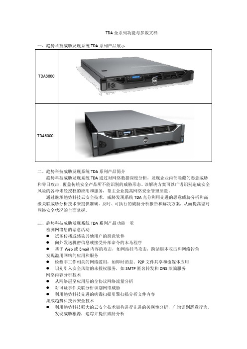
TDA全系列功能与参数文档二、趋势科技威胁发现系统TDA系列产品简介趋势科技威胁发现系统TDA通过对网络数据深度分析,发现企业内部隐藏的恶意威胁和零日攻击,覆盖传统安全产品所不能识别的威胁形态。
该解决方案可以广谱识别造成安全风险的各种未经授权的应用和服务,帮主企业提高网络安全管理质量。
通过继承趋势科技云安全技术,威胁发现系统TDA充分利用先进的恶意威胁分析和高级关联威胁分析技术来提供准确、及时、可执行的威胁分析报告和解决方案,从而提高您对网络安全状况的全面掌握。
三、趋势科技威胁发现系统TDA系列产品功能一览检测网络层的恶意活动●试图传播或感染其他用户的恶意软件●向外发送机密信息或接受外部命令的木马程序●基于Web或Email内容的攻击,如网站挂马攻击,跨站脚本攻击和网络钓鱼发现滥用网络的应用和服务●检测非工作相关的网络滥用,如即时消息、P2P文件共享和流媒体应用●识别引入安全风险的未授权服务,如SMTP匿名转发和DNS欺骗服务网络内容分析技术●从网络层至应用层的全协议网络流量分析●对可疑事件关联分析识别网络威胁●利用趋势科技先进的病毒扫描引擎扫描分析文件内容集成趋势科技云安全技术●利用趋势科技强大的云安全技术架构进行先进的关联性分析,广谱识别恶意行为,发现威胁根源,追踪并提供威胁分析●充分利用趋势科技云安全技术对最新出现的安全威胁进行识别和分析●访问趋势科技的安全情报中心,可以获得详细而及时的最新威胁状况威胁分析和报表功能●自动生成企业安全形势的总体视图●集中管理的报表和安全事件信息●自动生成每日时间报表,同时提供/月报表以查看整体安全状况●通过实践信息浏览生成更为详细的交互式报表●显示综合威胁信息的详细视图●提供安全策略优化、可执行的安全措施和安全响应建议四、趋势科技威胁发现系统TDA系列产品参数。
TDA5200中文数据手册
(一)被植入人体,或(b)支持和/或维护和保持人的生命,生命支持设备或系统的目的.如果他们 失败,这是合理的假设,可能会危害用户的健康.
产品信息
概述
该IC是一个非常低的功耗.
包
TION单芯片ASK单次转换
SION接收机的频带
868-870 MHz和433-435 MHz的. “
IC提供了高集成度,只需要少量的外部元件.该
5.1.1绝对最大额定值. . . . . . . . . . . . . . . . . . . . . . . . . . . . . . . . . . . . . . . . . . . . . . . .
5.1.2工作范围. . . . . . . . . . . . . . . . . . . . . . . . . . . . . . . . . . . . . . . . . . . . . . . . . . . . . . . .
对于包装材料返回到我们未分类的,我们没有义务接受,我们将不得不到发票所发生的任何费用.
在生命支持设备或系统使用的组件必须明确授权这样的目的!
关键部件
1 英飞凌科技股份公司,只能用于生命支持设备或系统
英飞凌科技股份公司.
2 明确书面许可,
1关键部件是在生命支持设备或系统,其故障可以合理预期造成的故障的生活使用的组件, 支持设备或系统,或影响其安全性和有效性,设备或系统.
i
2产品说明
..........................................................
2-1
2.1 概述. . . . . . . . . . . . . . . . . . . . . . . . . . . . . . . . . . . . . . . . . . . . . . . . . . . . . . . . . . . . . . .
- 1、下载文档前请自行甄别文档内容的完整性,平台不提供额外的编辑、内容补充、找答案等附加服务。
- 2、"仅部分预览"的文档,不可在线预览部分如存在完整性等问题,可反馈申请退款(可完整预览的文档不适用该条件!)。
- 3、如文档侵犯您的权益,请联系客服反馈,我们会尽快为您处理(人工客服工作时间:9:00-18:30)。
TDA全系列功能与参数文档
二、趋势科技威胁发现系统TDA系列产品简介
趋势科技威胁发现系统TDA通过对网络数据深度分析,发现企业内部隐藏的恶意威胁和零日攻击,覆盖传统安全产品所不能识别的威胁形态。
该解决方案可以广谱识别造成安全风险的各种未经授权的应用和服务,帮主企业提高网络安全管理质量。
通过继承趋势科技云安全技术,威胁发现系统TDA充分利用先进的恶意威胁分析和高级关联威胁分析技术来提供准确、及时、可执行的威胁分析报告和解决方案,从而提高您对网络安全状况的全面掌握。
三、趋势科技威胁发现系统TDA系列产品功能一览
检测网络层的恶意活动
●试图传播或感染其他用户的恶意软件
●向外发送机密信息或接受外部命令的木马程序
●基于Web或Email内容的攻击,如网站挂马攻击,跨站脚本攻击和网络钓鱼
发现滥用网络的应用和服务
●检测非工作相关的网络滥用,如即时消息、P2P文件共享和流媒体应用
●识别引入安全风险的未授权服务,如SMTP匿名转发和DNS欺骗服务
网络内容分析技术
●从网络层至应用层的全协议网络流量分析
●对可疑事件关联分析识别网络威胁
●利用趋势科技先进的病毒扫描引擎扫描分析文件内容
集成趋势科技云安全技术
●利用趋势科技强大的云安全技术架构进行先进的关联性分析,广谱识别恶意行为,
发现威胁根源,追踪并提供威胁分析
●充分利用趋势科技云安全技术对最新出现的安全威胁进行识别和分析●访问趋势科技的安全情报中心,可以获得详细而及时的最新威胁状况威胁分析和报表功能
●自动生成企业安全形势的总体视图
●集中管理的报表和安全事件信息
●自动生成每日时间报表,同时提供/月报表以查看整体安全状况
●通过实践信息浏览生成更为详细的交互式报表
●显示综合威胁信息的详细视图
●提供安全策略优化、可执行的安全措施和安全响应建议
四、趋势科技威胁发现系统TDA系列产品参数。