PCA9542APW-T中文资料
PCA9532BS,118;PCA9532PW,112;PCA9532D,112;PCA9532PW,118;PCA9532D,118;中文规格书,Datasheet资料
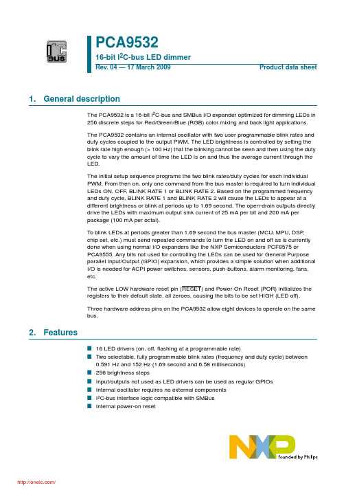
1.General descriptionThe PCA9532is a 16-bit I 2C-bus and SMBus I/O expander optimized for dimming LEDs in 256 discrete steps for Red/Green/Blue (RGB) color mixing and back light applications.The PCA9532 contains an internal oscillator with two user programmable blink rates and duty cycles coupled to the output PWM. The LED brightness is controlled by setting the blink rate high enough (>100Hz)that the blinking cannot be seen and then using the duty cycle to vary the amount of time the LED is on and thus the average current through the LED.The initial setup sequence programs the two blink rates/duty cycles for each individual PWM.From then on,only one command from the bus master is required to turn individual LEDs ON, OFF , BLINK RATE 1 or BLINK RATE 2. Based on the programmed frequency and duty cycle, BLINK RATE 1 and BLINK RA TE 2 will cause the LEDs to appear at a different brightness or blink at periods up to 1.69second. The open-drain outputs directly drive the LEDs with maximum output sink current of 25mA per bit and 200mA per package (100mA per octal).To blink LEDs at periods greater than 1.69second the bus master (MCU, MPU, DSP ,chip set, etc.) must send repeated commands to turn the LED on and off as is currently done when using normal I/O expanders like the NXP Semiconductors PCF8575 or PCA9555. Any bits not used for controlling the LEDs can be used for General Purpose parallel Input/Output (GPIO)expansion,which provides a simple solution when additional I/O is needed for ACPI power switches, sensors, push-buttons, alarm monitoring, fans,etc.The active LOW hardware reset pin (RESET) and Power-On Reset (POR) initializes the registers to their default state, all zeroes, causing the bits to be set HIGH (LED off).Three hardware address pins on the PCA9532allow eight devices to operate on the same bus.2.FeaturesI 16 LED drivers (on, off, flashing at a programmable rate)I Two selectable, fully programmable blink rates (frequency and duty cycle) between 0.591Hz and 152Hz (1.69second and 6.58milliseconds)I 256 brightness stepsI Input/outputs not used as LED drivers can be used as regular GPIOs I Internal oscillator requires no external components I I 2C-bus interface logic compatible with SMBus I Internal power-on resetPCA953216-bit I 2C-bus LED dimmerRev. 04 — 17 March 2009Product data sheetI Noise filter on SCL/SDA inputs I Active LOW reset inputI 16 open-drain outputs directly drive LEDs to 25mA I Controlled edge rates to minimize ground bounce I No glitch on power-up I Supports hot insertion I Low standby currentI Operating power supply voltage range of 2.3V to 5.5V I 0Hz to 400kHz clock frequencyIESD protection exceeds 2000V HBM per JESD22-A114, 150V MM per JESD22-A115 and 1000V CDM per JESD22-C101I Latch-up testing is done to JEDEC Standard JESD78 which exceeds 100 mA I Packages offered: SO24, TSSOP24, HVQFN243.Ordering information4.Block diagramTable 1.Ordering information T amb =−40°C to +85°C.Type number Topside mark Package Name DescriptionVersion PCA9532D PCA9532D SO24plastic small outline package; 24leads; body width 7.5mm SOT137-1PCA9532PW PCA9532TSSOP24plastic thin shrink small outline package; 24leads;body width 4.4mmSOT355-1PCA9532BS9532HVQFN24plastic thermal enhanced very thin quad flat package; no leads;24terminals; body 4×4×0.85mmSOT616-1Only one I/O shown for clarity.Fig 1.Block diagram of PCA9532A0A1A2002aae521I 2C-BUS CONTROLINPUT FILTERSPCA9532POWER-ON RESETSCL SDAV DD V SSLEDnRESETOSCILLATORPRESCALER 1REGISTERPRESCALER 0REGISTER PWM1REGISTERPWM0REGISTER INPUT REGISTERLED SELECT (LSn)REGISTERBLINK0BLINK115.Pinning information5.1PinningFig 2.Pin configuration for SO24Fig 3.Pin configuration for TSSOP24Fig 4.Pin configuration for HVQFN24PCA9532D A0V DD A1SDA A2SCL LED0RESET LED1LED15LED2LED14LED3LED13LED4LED12LED5LED11LED6LED10LED7LED9V SS LED8002aae518123456789101112141316151817201922212423V DD SDA SCL RESET LED15LED14LED13LED12LED11LED10LED9LED8A0A1A2LED0LED1LED2LED3LED4LED5LED6LED7V SS PCA9532PW002aae519123456789101112141316151817201922212423002aae520PCA9532BST ransparent top viewLED11LED4LED5LED12LED3LED13LED2LED14LED1LED15LED0RESET L E D 6L E D 7V S SL E D 8L E D 9L E D 10A 2A 1A 0V D DS D AS C Lterminal 1index area6135144153162171187891011122423222120195.2Pin description[1]HVQFN24 package die supply ground is connected to both V SS pin and exposed center pad. V SS pin must be connected to supply ground for proper device operation. For enhanced thermal, electrical, and board level performance, the exposed pad needs to be soldered to the board using a corresponding thermal pad on the board and for proper heat conduction through the board,thermal vias need to be incorporated in the PCB in the thermal pad region.Table 2.Pin descriptionSymbolPin DescriptionSO24,TSSOP24HVQFN24A0122address input 0A1223address input 1A2324address input 2LED041LED driver 0LED152LED driver 1LED263LED driver 2LED374LED driver 3LED485LED driver 4LED596LED driver 5LED6107LED driver 6LED7118LED driver 7V SS 129[1]supply ground LED81310LED driver 8LED91411LED driver 9LED101512LED driver 10LED111613LED driver 11LED121714LED driver 12LED131815LED driver 13LED141916LED driver 14LED152017LED driver 15RESET 2118reset input (active LOW)SCL 2219serial clock line SDA 2320serial data line V DD2421supply voltage6.Functional descriptionRefer to Figure 1 “Block diagram of PCA9532”.6.1Device addressFollowing a START condition, the bus master must output the address of the slave it is accessing. The address of the PCA9532 is shown in Figure 5. To conserve power, no internal pull-up resistors are incorporated on the hardware selectable address pins and they must be pulled HIGH or LOW.The last bit of the address byte defines the operation to be performed.When set to logic 1a read is selected, while a logic 0 selects a write operation.6.2Control registerFollowing the successful acknowledgement of the slave address,the bus master will send a byte to the PCA9532, which will be stored in the Control register.The lowest 4bits are used as a pointer to determine which register will be accessed.If the Auto-Increment (AI) flag is set, the four low order bits of the Control register are automatically incremented after a read or write. This allows the user to program the registers sequentially. The contents of these bits will rollover to ‘0000’ after the last register is accessed.When Auto-Increment flag is set (AI =1) and a read sequence is initiated, the sequence must start by reading a register different from the INPUT0 register (B3B2B1B0≠0000).Only the 4 least significant bits are affected by the AI flag. Unused bits must be programmed with zeroes.Fig 5.PCA9532 slave address002aac50511A2A1A0R/Wfixedslave addresshardware selectableReset state: 00hFig 6.Control register002aae523000AI B3B2B1B0register addressAuto-Increment flag6.2.1Control register definitionTable 3.Register summaryB3B2B1B0Symbol Access Description0000INPUT0read only input register 00001INPUT1read only input register 10010PSC0read/write frequency prescaler 00011PWM0read/write PWM register 00100PSC1read/write frequency prescaler 10101PWM1read/write PWM register 10110LS0read/write LED0 to LED3 selector0111LS1read/write LED4 to LED7 selector1000LS2read/write LED8 to LED11 selector1001LS3read/write LED12 to LED15 selector6.3Register descriptions6.3.1INPUT0 - Input register 0The INPUT0register reflects the state of the device pins (inputs 0 to 7). Writes to thisregister will be acknowledged but will have no effect.Table 4.INPUT0 - Input register 0 descriptionBit76543210Symbol LED7LED6LED5LED4LED3LED2LED1LED0Default X X X X X X X XRemark:The default value‘X’is determined by the externally applied logic level(normally logic1) when used for directly driving LED with pull-up to V DD.6.3.2INPUT1 - Input register 1The INPUT1 register reflects the state of the device pins (inputs 8 to 15). Writes to thisregister will be acknowledged but will have no effect.Table 5.INPUT1 - Input register 1 descriptionBit76543210Symbol LED15LED14LED13LED12LED11LED10LED9LED8Default X X X X X X X XRemark:The default value‘X’is determined by the externally applied logic level(normally logic1) when used for directly driving LED with pull-up to V DD.6.3.3PCS0 - Frequency Prescaler 0PSC0 is used to program the period of the PWM output.The period of BLINK0=(PSC0+1)/152.6.3.4PWM0 - Pulse Width Modulation 0The PWM0register determines the duty cycle of BLINK0.The outputs are LOW (LED on)when the count is less than the value in PWM0 and HIGH (LED off) when it is greater. If PWM0 is programmed with 00h, then the PWM0 output is always HIGH (LED off).The duty cycle of BLINK0=PWM0/256.6.3.5PCS1 - Frequency Prescaler 1PSC1 is used to program the period of the PWM output.The period of BLINK1=(PSC1+1)/152.6.3.6PWM1 - Pulse Width Modulation 1The PWM1register determines the duty cycle of BLINK1.The outputs are LOW (LED on)when the count is less than the value in PWM1 and HIGH (LED off) when it is greater. If PWM1 is programmed with 00h, then the PWM1 output is always HIGH (LED off).The duty cycle of BLINK1=PWM1/256.Table 6.PSC0 - Frequency Prescaler 0 register descriptionBit 76543210Symbol PSC0[7]PSC0[6]PSC0[5]PSC0[4]PSC0[3]PSC0[2]PSC0[1]PSC0[0]DefaultTable 7.PWM0 - Pulse Width Modulation 0 register descriptionBit 76543210Symbol PWM0[7]PWM0[6]PWM0[5]PWM0[4]PWM0[3]PWM0[2]PWM0[1]PWM0[0]Default1Table 8.PSC1 - Frequency Prescaler 1 register descriptionBit 76543210Symbol PSC1[7]PSC1[6]PSC1[5]PSC1[4]PSC1[3]PSC1[2]PSC1[1]PSC1[0]DefaultTable 9.PWM1 - Pulse Width Modulation 1 register descriptionBit 76543210Symbol PWM1[7]PWM1[6]PWM1[5]PWM1[4]PWM1[3]PWM1[2]PWM1[1]PWM1[0]Default16.3.7LS0 to LS3 - LED selector registersThe LSn LED selector registers determine the source of the LED data.00=output is set high-impedance (LED off; default)01=output is set LOW (LED on)10=output blinks at PWM0 rate11=output blinks at PWM1 rateTable 10.LS0 to LS3 - LED selector registers bit descriptionLegend: * default value.Register Bit Value DescriptionLS0 - LED0 to LED3 selectorLS07:600*LED3 selected5:400*LED2 selected3:200*LED1 selected1:000*LED0 selectedLS1 - LED4 to LED7 selectorLS17:600*LED7 selected5:400*LED6 selected3:200*LED5 selected1:000*LED4 selectedLS2 - LED8 to LED11 selectorLS27:600*LED11 selected5:400*LED10 selected3:200*LED9 selected1:000*LED8 selectedLS3 - LED12 to LED15 selectorLS37:600*LED15 selected5:400*LED14 selected3:200*LED13 selected1:000*LED12 selected6.4Pins used as GPIOsLEDn pins not used to control LEDs can be used as General Purpose I/Os (GPIOs).For use as input, set LEDn to high-impedance (00) and then read the pin state via the INPUT0 or INPUT1 register.For use as output, connect external pull-up resistor to the pin and size it according to the DC recommended operating characteristics. LEDn output pin is HIGH when the output is programmed as high-impedance,and LOW when the output is programmed LOW through the ‘LED selector’ register. The output can be pulse-width controlled when PWM0 orPWM1 are used.6.5Power-on resetWhen power is applied to V DD, an internal Power-On Reset (POR) holds the PCA9532 ina reset condition until V DD has reached V POR.At that point,the reset condition is releasedand the PCA9532 registers are initialized to their default states, all the outputs in theOFF state. Thereafter, V DD must be lowered below 0.2V to reset the device.6.6External RESETA reset can be accomplished by holding the RESET pin LOW for a minimum of t w(rst).ThePCA9532 registers and I2C-bus state machine will be held in their default states until the RESET input is once again HIGH.This input requires a pull-up resistor to V DD if no active connection is used.7.Characteristics of the I 2C-busThe I 2C-bus is for 2-way,2-line communication between different ICs or modules.The two lines are a serial data line (SDA) and a serial clock line (SCL). Both lines must beconnected to a positive supply via a pull-up resistor when connected to the output stages of a device. Data transfer may be initiated only when the bus is not busy.7.1Bit transferOne data bit is transferred during each clock pulse.The data on the SDA line must remain stable during the HIGH period of the clock pulse as changes in the data line at this time will be interpreted as control signals (see Figure 7).7.1.1START and STOP conditionsBoth data and clock lines remain HIGH when the bus is not busy. A HIGH-to-LOWtransition of the data line while the clock is HIGH is defined as the START condition (S).A LOW-to-HIGH transition of the data line while the clock is HIGH is defined as the STOP condition (P) (see Figure 8).7.2System configurationA device generating a message is a ‘transmitter’; a device receiving is the ‘receiver’. The device that controls the message is the ‘master’ and the devices which are controlled by the master are the ‘slaves’ (see Figure 9).Fig 7.Bit transfermba607data line stable;data validchange of data allowedSDASCLFig 8.Definition of START and STOP conditionsmba608SDASCLPSTOP conditionSSTART condition分销商库存信息:NXPPCA9532BS,118PCA9532PW,112PCA9532D,112 PCA9532PW,118PCA9532D,118。
新明和成面具使用说明书
GB2626-2006自吸过滤式防颗粒物呼吸器[可更换式半面罩 分类:KP95]CDR28SU2W 使用说明书截至2014年4月日本制造 Made in JapanIIMK720000 AC感谢您购买本产品。
请务必在使用前详细阅读本说明书,在充分理解内容的基础上正确使用。
请保管好本说明书以便随时能够阅读。
■警报标记的定义本文中标示的[危险][警告][注意]标记是为了防止错误操作、避免发生事故而记载的重要内容,请仔细阅读并安全使用。
各标记含义如下。
■使用时的注意事项为安全使用本产品,请严格遵守以下事项。
错误使用有可能导致使用者的生命处于危险状态。
■保养方法《过滤器》晾干过滤器,轻轻拍掉附着在过滤器上的粉尘,此时小心粉尘飞散。
1. 用干布或者稍微浸湿的布擦拭附着在罩体、吸气阀、排气阀、排气阀座、松紧带等上的灰尘、汗水等污垢。
2. 污垢严重时,请拆下过滤器,用含有少量中性洗涤剂的温水或水浸湿的海绵等清洗过滤器之外的部分。
然后用水冲洗干净,晾干。
3. 用消毒用酒精擦拭过后,为避免酒精残留,请充分晾干面具。
■保管条件温度0℃~50℃湿度75%以下■更换标准若符合下面情况时,请更换过滤器或零部件。
《过滤器》1. 过滤器有收缩、破损、明显的变形时。
2. 吸气阻力很明显上升时或者粉尘过滤效率下降时。
《排气阀、吸气阀》有破损、龟裂、明显的变形或发粘时。
《松紧带》1. 由于老化失去弹性,伸缩不良时。
2. 有龟裂、破损等时。
《垫圈》有破损、龟裂、明显变形,由于老化失去弹性时。
■废弃方法使用过的过滤器,必须遵守法律规定废弃。
废弃过滤器时,要把它放入气密性高的袋子,以免粉尘飞散。
■选购零部件●气密检查器R3检查气密性时使用的工具。
需要2个。
有关详细内容请阅读气密性检查方法。
●防火花盖E、F防止焊接火花飞入过滤器。
防火花盖F 带有气密检查器的功能。
●吸水垫片S2罩体内侧有呼气中的水分、汗水等时使用。
用水清洗后,可以反复使用。
PCA9545APWT中文资料
FEATURESRGY PACKAGE(TOP VIEW)2A119SDA3RESET18SCL4INT017INT5SD016SC36SC015SD37INT114INT38SD113SC29SC112SD2110AGND2011INT2VCCRESETINT0SD0SC0INT1INTSC3SD3INT3SC2RGW PACKAGE(TOP VIEW)SDASCLA1AVCCDGV,DW,OR PW PACKAGE(TOP VIEW)DESCRIPTION/ORDERING INFORMATIONSCPS147C–OCTOBER2005–REVISED OCTOBER2006•1-of-4Bidirectional Translating Switches•No Glitch on Power Up•I2C Bus and SMBus Compatible•Supports Hot Insertion•Four Active-Low Interrupt Inputs•Low Standby Current•Active-Low Interrupt Output•Operating Power-Supply Voltage Range of2.3V to5.5V•Active-Low Reset Input• 5.5-V Tolerant Inputs•Two Address Pins,Allowing up to FourDevices on the I2C Bus•0to400-kHz Clock Frequency•Channel Selection Via I2C Bus,In Any•Latch-Up Performance Exceeds100mA Per Combination JESD78•Power Up With All Switch Channels•ESD Protection Exceeds JESD22 Deselected–2000-V Human-Body Model(A114-A)•Low R ON Switches–200-V Machine Model(A115-A)•Allows Voltage-Level Translation Between–1000-V Charged-Device Model(C101)1.8-V,2.5-V,3.3-V,and5-V BusesThe PCA9545A is a quad bidirectional translating switch controlled via the I2C bus.The SCL/SDA upstream pair fans out to four downstream pairs,or channels.Any individual SCn/SDn channel or combination of channels can be selected,determined by the contents of the programmable control register.Four interrupt inputs(INT3–INT0), one for each of the downstream pairs,are provided.One interrupt(INT)output acts as an AND of the four interrupt inputs.An active-low reset(RESET)input allows the PCA9545A to recover from a situation in which one of the downstream I2C buses is stuck in a low state.Pulling RESET low resets the I2C state machine and causes all the channels to be deselected,as does the internal power-on reset function.The pass gates of the switches are constructed such that the V CC pin can be used to limit the maximum high voltage,which will be passed by the PCA9545A.This allows the use of different bus voltages on each pair,so that1.8-V,2.5-V,or3.3-V parts can communicate with5-V parts,without any additional protection.External pullup resistors pull the bus up to the desired voltage level for each channel.All I/O pins are5.5-V tolerant.Please be aware that an important notice concerning availability,standard warranty,and use in critical applications of TexasInstruments semiconductor products and disclaimers thereto appears at the end of this data sheet.PRODUCTION DATA information is current as of publication date.Copyright©2005–2006,Texas Instruments Incorporated Products conform to specifications per the terms of the TexasInstruments standard warranty.Production processing does notnecessarily include testing of all parameters.DESCRIPTION/ORDERING INFORMATION (CONTINUED)GQN OR ZQN PACKAGE(TOP VIEW)1234A B C D ESCPS147C–OCTOBER 2005–REVISED OCTOBER 2006ORDERING INFORMATIONT APACKAGE (1)ORDERABLE PART NUMBER TOP-SIDE MARKING QFN –RGW Reel of 3000PCA9545ARGWR PD545A QFN –RGY Reel of 1000PCA9545ARGYR PD545A Tube of 25PCA9545ADW PCA9545A SOIC –DWReel of 2000PCA9545ADWR Reel of 250PCA9545ADWT PCA9545A PCA9545APW PD545ATube of 70PCA9545APWE4–40°C to 85°CPCA9545APWR PD545ATSSOP –PWReel of 2000PCA9545APWRE4PCA9545APWT PD545A Reel of 250PCA9545APWTE4Reel of 2000PCA9545ADGVR TVSOP –DGV PD545A Reel of 250PCA9545ADGVT VFBGA –GQNReel of 1000PCA9545AGQNR PD545A VFBGA –ZQN (Pb-free)Reel of 1000PCA9545AZQNRPD545A (1)Package drawings,standard packing quantities,thermal data,symbolization,and PCB design guidelines are available at /sc/package.TERMINAL ASSIGNMENTS1234A A1A0V CC SDA B INT0INT RESET SCL C SC0SD0SD3SC3D SD1SC2INT1INT3EGNDSC1INT2SD22Submit Documentation FeedbackSCPS147C–OCTOBER2005–REVISED OCTOBER2006TERMINAL FUNCTIONSNO.NAME DESCRIPTIONDGV,DW,PW,GQN ANDRGWAND RGY ZQN119A2A0Address input0.Connect directly to V CC or ground.220A1A1Address input1.Connect directly to V CC or ground.Active-low reset input.Connect to V CC through a pullup 31B3RESETresistor,if not used.Active-low interrupt input0.Connect to V CC through a 42B1INT0pullup resistor.53C2SD0Serial data0.Connect to V CC through a pullup resistor.64C1SC0Serial clock0.Connect to V CC through a pullup resistor.Active-low interrupt input1.Connect to V CC through a 75D3INT1pullup resistor.86D1SD1Serial data1.Connect to V CC through a pullup resistor.97E2SC1Serial clock1.Connect to V CC through a pullup resistor.108E1GND GroundActive-low interrupt input2.Connect to V CC through a 119E3INT2pullup resistor.1210E4SD2Serial data2.Connect to V CC through a pullup resistor.1311D2SC2Serial clock2.Connect to V CC through a pullup resistor.Active-low interrupt input3.Connect to V CC through a 1412D4INT3pullup resistor.1513C3SD3Serial data3.Connect to V CC through a pullup resistor.1614C4SC3Serial clock3.Connect to V CC through a pullup resistor.Active-low interrupt output.Connect to V CC through a pullup 1715B2INTresistor.1816B4SCL Serial clock line.Connect to V CC through a pullup resistor.1917A4SDA Serial data line.Connect to V CC through a pullup resistor.2018A3V CC Supply power3Submit Documentation FeedbackSCPS147C–OCTOBER2005–REVISED OCTOBER2006BLOCK DIAGRAMPin numbers shown are for DGV, DW, PW, and RGY packages.4Submit Documentation FeedbackDevice AddressFixedHardware SelectableControl RegisterInterrupt Bits (Read Only)Channel-Selection Bits(Read/Write)Channel 0Channel 1Channel 2Channel 3INT0INT1INT2INT3Control Register DefinitionSCPS147C–OCTOBER 2005–REVISED OCTOBER 2006Following a start condition,the bus master must output the address of the slave it is accessing.The address of the PCA9545A is shown in Figure 1.To conserve power,no internal pullup resistors are incorporated on the hardware-selectable address they must be pulled high or low.Figure 1.PCA9545A AddressThe last bit of the slave address defines the operation to be performed.When set to a logic 1,a read is selected,while a logic 0selects a write operation.Following the successful acknowledgment of the slave address,the bus master sends a byte to the PCA9545A,which is stored in the control register (see Figure 2).If multiple bytes are received by the PCA9545A,it saves the last byte received.This register can be written and read via the I 2C bus.Figure 2.Control RegisterOne or several SCn/SDn downstream pairs,or channels,are selected by the contents of the control register (see Table 1).After the PCA9545A has been addressed,the control register is written.The four LSBs of the used to determine which channel or channels are to be selected.When a channel is selected,the channel becomes active after a stop condition has been placed on the I 2C bus.This ensures that all SCn/SDn lines are in a high state when the channel is made active,so that no false conditions are generated at the time of connection.A stop condition must occur always right after the acknowledge cycle.5Submit Documentation FeedbackInterrupt HandlingSCPS147C–OCTOBER 2005–REVISED OCTOBER 2006Table 1.Control Register Write (Channel Selection),Control Register Read (Channel Status)(1)INT3INT2INT1INT0D3B2B1B0COMMAND0Channel 0disabled X X X X X X X 1Channel 0enabled 0Channel 1disabled X X X X X X X 1Channel 1enabled 0Channel 2disabled X X X X X X X 1Channel 2enabled 0Channel 3disabled X X X X X X X 1Channel 3enabledNo channel selected,00Xpower-up/reset default state(1)Several channels can be enabled at the same time.For example,B3=0,B2=1,B1=1,B0=0means that channels 0and 3are disabled,and channels 1are 2and enabled.Care should be taken not to exceed the maximum bus capacity.The PCA9545A provides four interrupt inputs (one for each channel)and one open-drain interrupt output (see Table 2).When an interrupt is generated by any device,it is detected by the PCA9545A and the interrupt output low.The channel does not need to be active for detection of the interrupt.A bit also is set in the control register.Bits 4–7of the control register correspond to channels 0–3of the PCA9545A,respectively.Therefore,if an interrupt is generated by any device connected to channel 1,the state of the interrupt inputs is loaded into the control register when a read is accomplished.Likewise,an interrupt on any device connected to channel 0would cause bit 4of the control register to be set on the read.The master then can address the PCA9545A and read the contents of the control register to determine which channel contains the device generating the interrupt.The master then can reconfigure the PCA9545A to select this channel and locate the device generating the interrupt and clear it.It should be noted that more than one device can provide an interrupt on a channel,so it is up to the master to ensure that all devices on a channel are interrogated for an interrupt.The interrupt inputs can be used as general-purpose inputs if the interrupt function is not required.If unused,interrupt input(s)must be connected to V CC .Table 2.Control Register Read (Interrupt)(1)INT3INT2INT1INT0D3B2B1B0COMMAND0No interrupt on channel 0X X X X X X X 1Interrupt on channel 00No interrupt on channel 1X X X X X X X 1Interrupt on channel 10No interrupt on channel 2X X X X X X X 1Interrupt on channel 20No interrupt on channel 3XXXXXXX1Interrupt on channel 3(1)Several interrupts can be active at the same time.For example,INT3=0,INT2=1,INT1=1,INT0=0means that there is no interrupt on channels 0and 3,and there is interrupt on channels 1and 2.6Submit Documentation FeedbackRESET InputPower-On ResetVoltage TranslationV CC (V)32.52V p a s s (V )I 2C InterfaceSCPS147C–OCTOBER 2005–REVISED OCTOBER 2006The RESET input can be used to recover the PCA9545A from a bus-fault condition.The registers and the I 2C state machine within this device initialize to their default states if this signal is asserted low for a minimum of t WL .All channels also are deselected in this case.RESET must be connected to V CC through a pullup resistor.When power is applied to V CC ,an internal power-on reset holds the PCA9545A in a reset condition until V CC has reached V POR .At this point,the reset condition is released and the PCA9545A registers and I 2C state machine are initialized to their default states,all zeroes,causing all the channels to be deselected.Thereafter,V CC must be lowered below 0.2V to reset the device.The pass-gate transistors of the PCA9545A are constructed such that the V CC voltage can be used to limit the maximum voltage that is passed from one I 2C bus to another.Figure 3shows the voltage characteristics of the pass-gate transistors (note that the graph was generated using in the electrical characteristics section of this data sheet).In order for the PCA9545A to act as a voltage translator,the V pass voltage must be equal to or lower than the lowest bus voltage.For example,if the main bus is running at 5V and the downstream buses are 3.3V and 2.7V,V pass must be equal to or below 2.7V to effectively clamp the downstream bus voltages.As shown in Figure 3,V pass (max)is at 2.7V when the PCA9545A supply voltage is 3.5V or lower,so the PCA9545A could be set to 3.3V.Pullup resistors then can be used to bring the bus voltages to their appropriate levels (see Figure 13).Figure 3.V pass Voltage vs V CCThe I 2C bus is for two-way two-line communication between different ICs or modules.The two lines are a serial data line (SDA)and a serial clock line (SCL).Both lines must be connected to a positive supply via a pullup resistor when connected to the output stages of a device.Data transfer can be initiated only when the bus is not busy.One data bit is transferred during each clock pulse.The data on the SDA line must remain stable during the high period of the clock pulse,as changes in the data line at this time are interpreted as control signals (see Figure 4).7Submit Documentation FeedbackSDASCLData Line Stable;Data ValidChange of Data AllowedSDASCLStart ConditionS Stop ConditionP SCLSDA SCPS147C–OCTOBER 2005–REVISED OCTOBER 2006Figure 4.Bit TransferBoth data and clock lines remain high when the bus is not busy.A high-to-low transition of the data line while the clock is high is defined as the start condition (S).A low-to-high transition of the data line while the clock is high is defined as the stop condition (P)(see Figure 5).Figure 5.Definition of Start and Stop ConditionsA device generating a message is a transmitter;a device receiving a message is the receiver.The device that controls the message is the master,and the devices that are controlled by the master are the slaves (see Figure 6).Figure 6.System ConfigurationThe number of data bytes transferred between the start and the stop conditions from transmitter to receiver is not limited.Each byte of eight bits is followed by one acknowlege (ACK)bit.The transmitter must release the SDA line before the receiver can send an ACK bit.When a slave receiver is addressed,it must generate an ACK after the reception of each byte.Also,a master must generate an ACK after the reception of each byte that has been clocked out of the slave transmitter.The device that acknowledges must pull down the SDA line during the ACK clock pulse so that the SDA line is stable low during the high pulse of the ACK-related clock period (see Figure 7).Setup and hold times must be taken into account.8Submit Documentation FeedbackData Output by TransmitterSCL FromMasterStart ConditionData Output by ReceiverClock Pulse for ACKSDASDA Start Condition R/W ACK From Slave NACK From Master Stop ConditionSCPS147C–OCTOBER 2005–REVISED OCTOBER 2006Figure 7.Acknowledgment on the I 2C BusA master receiver must signal an end of data to the transmitter by not generating an acknowledge (NACK)after the last byte has been clocked out of the slave.This is done by the master receiver by holding the SDA line high.In this event,the transmitter must release the data line to enable the master to generate a stop condition.Data is transmitted to the PCA9545A control register using the write mode shown in Figure 8.Figure 8.Write Control RegisterData is read from the PCA9545A control register using the read mode shown in Figure 9.Figure 9.Read Control Register9Submit Documentation FeedbackAbsolute Maximum Ratings (1)Recommended Operating Conditions (1)SCPS147C–OCTOBER 2005–REVISED OCTOBER 2006over operating free-air temperature range (unless otherwise noted)MINMAXUNIT V CC Supply voltage range –0.57V V I Input voltage range (2)–0.57V I I Input current ±20mA I OOutput current±25mA Continuous current through V CC ±100mA Continuous current through GND±100mADGV package 92DW package58GQN/ZQN package 78θJAPackage thermal impedance (3)°C/W PW package 83RGW package TBD RGY package47P tot Total power dissipation 400mW T stg Storage temperature range–65150°C T A Operating free-air temperature range–4085°C (1)Stresses beyond those listed under "absolute maximum ratings"may cause permanent damage to the device.These are stress ratings only,and functional operation of the device at these or any other conditions beyond those indicated under "recommended operating conditions"is not implied.Exposure to absolute-maximum-rated conditions for extended periods may affect device reliability.(2)The input negative-voltage and output voltage ratings may be exceeded if the input and output current ratings are observed.(3)The package thermal impedance is calculated in accordance with JESD 51-7.MINMAX UNIT V CC Supply voltage 2.3 5.5V SCL,SDA0.7×V CC 6V IH High-level input voltage V A1,A0,INT3–INT0,RESET 0.7×V CCV CC +0.5SCL,SDA–0.50.3×V CC V IL Low-level input voltage V A1,A0,INT3–INT0,RESET–0.50.3×V CCT A Operating free-air temperature–4085°C(1)All unused inputs of the device must be held at V CC or GND to ensure proper device operation.Refer to the TI application report,Implications of Slow or Floating CMOS Inputs ,literature number SCBA004.10Submit Documentation FeedbackElectrical CharacteristicsPCA9545A4-CHANNEL I2C AND SMBus SWITCH WITH INTERRUPT LOGIC AND RESET FUNCTIONSSCPS147C–OCTOBER2005–REVISED OCTOBER2006over recommended operating free-air temperature range(unless otherwise noted)PARAMETER TEST CONDITIONS V CC MIN TYP(1)MAX UNIT V POR Power-on reset voltage(2)No load,V I=V CC or GND V POR 1.6 2.1V5V 3.64.5V to5.5V 2.6 4.53.3V 1.9V pass Switch output voltage V SWin=V CC,I SWout=–100µA V3V to3.6V 1.6 2.82.5V 1.52.3V to2.7V 1.12I OH INT V O=V CC 2.3V to5.5V10µAV OL=0.4V37SCL,SDAI OL V OL=0.6V 2.3V to5.5V610mAINT V OL=0.4V3SCL,SDA±1SC3–SC0,SD3–SD0±1I I A1,A0V I=V CC or GND 2.3V to5.5V±1µAINT3–INT0±1RESET±15.5V312Operating mode f SCL=100kHz V I=V CC or GND,I O=0 3.6V3112.7V3105.5V0.31I CC Low inputs V I=GND,I O=0 3.6V0.11µA2.7V0.11Standby mode5.5V0.31High inputs V I=V CC,I O=0 3.6V0.112.7V0.11One INT3–INT0input at0.6V,815Other inputs at V CC or GNDINT3–INT0One INT3–INT0input at V CC–0.6V,815Other inputs at V CC or GNDSupply-current∆I CC 2.3V to5.5VµA change SCL or SDA input at0.6V,815Other inputs at V CC or GNDSCL,SDASCL or SDA input at V CC–0.6V,815Other inputs at V CC or GNDA1,A0 4.56C i INT3–INT0V I=V CC or GND 2.3V to5.5V 4.56pFRESET 4.5 5.5SCL,SDA1519C io(OFF)(3)V I=V CC or GND,Switch OFF 2.3V to5.5V pFSC3–SC0,SD3–SD0684.5V to5.5V4916V O=0.4V,I O=15mAR ON Switch on-state resistance3V to3.6V51120ΩV O=0.4V,I O=10mA 2.3V to2.7V71645(1)All typical values are at nominal supply voltage(2.5-V,3.3-V,or5-V V CC),T A=25°C.(2)The power-on reset circuit resets the I2C bus logic with V CC<V POR.V CC must be lowered to0.2V to reset the device.(3)C io(ON)depends on the device capacitance and load that is downstream from the device.元器件交易网I 2C Interface Timing RequirementsSwitching CharacteristicsPCA9545A4-CHANNEL I 2C AND SMBus SWITCHWITH INTERRUPT LOGIC AND RESET FUNCTIONSSCPS147C–OCTOBER 2005–REVISED OCTOBER 2006over recommended operating free-air temperature range (unless otherwise noted)(see Figure 10)STANDARD MODEFAST MODE I 2C BUSI 2C BUSUNITMINMAX MIN MAX f scl I 2C clock frequency 01000400kHz t sch I 2C clock high time 40.6µs t scl I 2C clock low time 4.71.3µs t sp I 2C spike time5050ns t sds I 2C serial-data setup time 250100ns t sdh I 2C serial-data hold time 0(1)0(1)µs t icr I 2C input rise time 100020+0.1C b (2)300ns t icf I 2C input fall time 30020+0.1C b (2)300ns t ocf I 2C output fall time10-pF to 400-pF bus30020+0.1C b (2)300ns t buf I 2C bus free time between stop and start 4.7 1.3µs t sts I 2C start or repeated start condition setup 4.70.6µs t sth I 2C start or repeated start condition hold 40.6µs t sps I 2C stop condition setup 40.6µs SCL low to SDA output low t vdL(Data)Valid-data time (high to low)(3)11µs validSCL low to SDA output high t vdH(Data)Valid-data time (low to high)(3)0.60.6µs validACK signal from SCL low t vd(ack)Valid-data time of ACK condition 11µs to SDA output lowC b I 2C bus capacitive load400400pF (1)A device internally must provide a hold time of at least 300ns for the SDA signal (referred to as the V IH min of the SCL signal),in order to bridge the undefined region of the falling edge of SCL.(2)C b =total bus capacitance of one bus line in pF(3)Data taken using a 1-k Ωpullup resistor and 50-pF load (see Figure 10)over recommended operating free-air temperature range,C L ≤100pF (unless otherwise noted)(see Figure 12)FROM TO PARAMETERMINMAX UNIT (INPUT)(OUTPUT)R ON =20Ω,C L =15pF 0.3t pd (1)Propagation delay time SDA or SCLSDn or SCnns R ON =20Ω,C L =50pF1t iv Interrupt valid time (2)INTn INT 4µs t ir Interrupt reset delay time (2)INTnINT2µs(1)The propagation delay is the calculated RC time constant of the typical ON-state resistance of the switch and the specified load capacitance,when driven by an ideal voltage source (zero output impedance).(2)Data taken using a 4.7-k Ωpullup resistor and 100-pF load (see Figure 12)元器件交易网Interrupt and Reset Timing RequirementsPCA9545A4-CHANNEL I2C AND SMBus SWITCH WITH INTERRUPT LOGIC AND RESET FUNCTIONSSCPS147C–OCTOBER2005–REVISED OCTOBER2006over recommended operating free-air temperature range(unless otherwise noted)(see Figure12)PARAMETER MIN MAX UNIT t PWRL Low-level pulse duration rejection of INTn inputs1µst PWRH High-level pulse duration rejection of INTn inputs0.5µst WL Pulse duration,RESET low6nst rst(1)RESET time(SDA clear)500nst REC(STA)Recovery time from RESET to start0ns(1)t rst is the propagation delay measured from the time the RESET pin is first asserted low to the time the SDA pin is asserted high,signaling a stop condition.It must be a minimum of t WL.元器件交易网PARAMETER MEASUREMENT INFORMATION= 1 k ΩL = 50 pF0.3 × V CCConditionConditionStart ConditionSCLSDAI 2C PORT LOAD CONFIGURATIONVOLTAGE WAVEFORMS0.7 × V CC0.3 × V CC0.7 × V CC PCA9545A4-CHANNEL I 2C AND SMBus SWITCHWITH INTERRUPT LOGIC AND RESET FUNCTIONSSCPS147C–OCTOBER 2005–REVISED OCTOBER 2006A.C L includes probe and jig capacitance.B.All input pulses are supplied by generators having the following characteristics:PRR ≤10MHz,Z O =50Ω,t r /t f =30ns.C.The outputs are measured one at a time,with one transition per measurement.Figure 10.I 2C Interface Load Circuit,Byte Descriptions,and Voltage Waveforms元器件交易网SCLSDALEDxRESETStartACK or Read CycleL = 4.7 k ΩL = 100 pF INTERRUPT LOAD CONFIGURATIONV CCINTn(input)VOLTAGE WAVEFORMS (t iv )VOLTAGE WAVEFORMS (t ir )INT (output)0.5 × V CCINTn (input)INT (output)× V CC0.5 × V CCPCA9545A4-CHANNEL I 2C AND SMBus SWITCHWITH INTERRUPT LOGIC AND RESET FUNCTIONSSCPS147C–OCTOBER 2005–REVISED OCTOBER 2006PARAMETER MEASUREMENT INFORMATION (continued)Figure 11.Reset TimingA.C L includes probe and jig capacitance.B.All input pulses are supplied by generators having the following characteristics:PRR ≤10MHz,Z O =50Ω,t r /t f =30ns.Figure 12.Interrupt Load Circuit and Voltage Waveforms元器件交易网APPLICATION INFORMATIONChannel 0Channel 1Channel 2Channel 3PCA9545A4-CHANNEL I 2C AND SMBus SWITCHWITH INTERRUPT LOGIC AND RESET FUNCTIONSSCPS147C–OCTOBER 2005–REVISED OCTOBER 2006Figure 13shows an application in which the PCA9545A can be used.A.If the device generating the interrupt has an open-drain output structure or can be 3-stated,a pullup resistor is required.If the device generating the interrupt has a totem-pole output structure and cannot be 3-stated,a pullup resistor is not required.The interrupt inputs should not be left floating.B.Pin numbers shown are for DGV,DW,PW,and RGY packages.Figure 13.Typical Application元器件交易网PACKAGING INFORMATIONOrderable Device Status (1)Package Type Package Drawing Pins Package Qty Eco Plan (2)Lead/Ball Finish MSL Peak Temp (3)PCA9545ADGVR ACTIVE TVSOP DGV 202000Green (RoHS &no Sb/Br)CU NIPDAU Level-1-260C-UNLIM PCA9545ADGVRG4ACTIVE TVSOP DGV202000Green (RoHS &no Sb/Br)CU NIPDAU Level-1-260C-UNLIM PCA9545ADGVT PREVIEW TVSOP DGV 20250TBD Call TI Call TIPCA9545ADW ACTIVE SOIC DW 2025Green (RoHS &no Sb/Br)CU NIPDAU Level-1-260C-UNLIM PCA9545ADWG4ACTIVE SOIC DW 2025Green (RoHS &no Sb/Br)CU NIPDAU Level-1-260C-UNLIM PCA9545ADWR ACTIVE SOIC DW 202000Green (RoHS &no Sb/Br)CU NIPDAU Level-1-260C-UNLIM PCA9545ADWRG4ACTIVE SOIC DW 202000Green (RoHS &no Sb/Br)CU NIPDAU Level-1-260C-UNLIM PCA9545ADWT PREVIEW SOIC DW 20250TBD Call TI Call TIPCA9545AGQNRNRNDBGA MI CROSTA R JUNI OR GQN201000TBDSNPBLevel-1-240C-UNLIMPCA9545APW ACTIVE TSSOP PW 2070Green (RoHS &no Sb/Br)CU NIPDAU Level-1-260C-UNLIM PCA9545APWE4ACTIVE TSSOP PW 2070Green (RoHS &no Sb/Br)CU NIPDAU Level-1-260C-UNLIM PCA9545APWG4ACTIVE TSSOP PW 2070Green (RoHS &no Sb/Br)CU NIPDAU Level-1-260C-UNLIM PCA9545APWR ACTIVE TSSOP PW 202000Green (RoHS &no Sb/Br)CU NIPDAU Level-1-260C-UNLIM PCA9545APWRE4ACTIVE TSSOP PW 202000Green (RoHS &no Sb/Br)CU NIPDAU Level-1-260C-UNLIM PCA9545APWRG4ACTIVE TSSOP PW 202000Green (RoHS &no Sb/Br)CU NIPDAU Level-1-260C-UNLIM PCA9545APWT ACTIVE TSSOP PW 20250Green (RoHS &no Sb/Br)CU NIPDAU Level-1-260C-UNLIM PCA9545APWTE4ACTIVE TSSOP PW 20250Green (RoHS &no Sb/Br)CU NIPDAU Level-1-260C-UNLIM PCA9545APWTG4ACTIVE TSSOP PW 20250Green (RoHS &no Sb/Br)CU NIPDAU Level-1-260C-UNLIM PCA9545ARGWR PREVIEW QFN RGW 203000TBDCall TI Call TIPCA9545ARGYR ACTIVE QFN RGY 201000Green (RoHS &no Sb/Br)CU NIPDAU Level-2-260C-1YEAR PCA9545ARGYRG4ACTIVE QFN RGY 201000Green (RoHS &no Sb/Br)CU NIPDAU Level-2-260C-1YEAR PCA9545AZQNRACTIVEBGA MI CROSTA R JUNI ORZQN201000Green (RoHS &no Sb/Br)SNAGCULevel-1-260C-UNLIM(1)The marketing status values are defined as follows:ACTIVE:Product device recommended for new designs.LIFEBUY:TI has announced that the device will be discontinued,and a lifetime-buy period is in effect.NRND:Not recommended for new designs.Device is in production to support existing customers,but TI does not recommend using this part in a new design.PREVIEW:Device has been announced but is not in production.Samples may or may not be available.OBSOLETE:TI has discontinued the production of the device.(2)Eco Plan-The planned eco-friendly classification:Pb-Free(RoHS),Pb-Free(RoHS Exempt),or Green(RoHS&no Sb/Br)-please check /productcontent for the latest availability information and additional product content details.TBD:The Pb-Free/Green conversion plan has not been defined.Pb-Free(RoHS):TI's terms"Lead-Free"or"Pb-Free"mean semiconductor products that are compatible with the current RoHS requirements for all6substances,including the requirement that lead not exceed0.1%by weight in homogeneous materials.Where designed to be soldered at high temperatures,TI Pb-Free products are suitable for use in specified lead-free processes.Pb-Free(RoHS Exempt):This component has a RoHS exemption for either1)lead-based flip-chip solder bumps used between the die and package,or2)lead-based die adhesive used between the die and leadframe.The component is otherwise considered Pb-Free(RoHS compatible)as defined above.Green(RoHS&no Sb/Br):TI defines"Green"to mean Pb-Free(RoHS compatible),and free of Bromine(Br)and Antimony(Sb)based flame retardants(Br or Sb do not exceed0.1%by weight in homogeneous material)(3)MSL,Peak Temp.--The Moisture Sensitivity Level rating according to the JEDEC industry standard classifications,and peak solder temperature.Important Information and Disclaimer:The information provided on this page represents TI's knowledge and belief as of the date that it is provided.TI bases its knowledge and belief on information provided by third parties,and makes no representation or warranty as to the accuracy of such information.Efforts are underway to better integrate information from third parties.TI has taken and continues to take reasonable steps to provide representative and accurate information but may not have conducted destructive testing or chemical analysis on incoming materials and chemicals.TI and TI suppliers consider certain information to be proprietary,and thus CAS numbers and other limited information may not be available for release.In no event shall TI's liability arising out of such information exceed the total purchase price of the TI part(s)at issue in this document sold by TI to Customer on an annual basis.。
PCA9548ARGERG4中文资料
RGE PACKAGE (TOP VIEW)
RESET A1 A0 VCC SDA SCL
24 23 22 21 20 19
2
Submit Documentation Feedback
元器件交易网
SC0 SC1 SC2 SC3 SC4 SC5 SC6 SC7 SD0 SD1 SD2 SD3 SD4 SD5 SD6 SD7
PCA9548A 8-CHANNEL I2C SWITCH
(2) Package drawings, standard packing quantities, thermal data, symbolization, and PCB design guidelines are available at /sc/package.
Please be aware that an important notice concerning availability, standard warranty, and use in critical applications of Texas Instruments semiconductor products and disclaimers thereto appears at the end of this data sheet.
Address input 0. Connect directly to VCC or ground. Address input 1. Connect directly to VCC or ground. Active-low reset input. Connect to VCC through a pullup resistor, if not used. Serial data 0. Connect to VCC through a pullup resistor. Serial clock 0. Connect to VCC through a pullup resistor. Serial data 1. Connect to VCC through a pullup resistor. Serial clock 1. Connect to VCC through a pullup resistor. Serial data 2. Connect to VCC through a pullup resistor. Serial clock 2. Connect to VCC through a pullup resistor. Serial data 3. Connect to VCC through a pullup resistor. Serial clock 3. Connect to VCC through a pullup resistor. Ground
9540认证解读 -回复
9540认证解读-回复什么是9540认证,以及它的解读。
首先,我们来了解一下9540认证是什么。
9540认证是中国国家标准化委员会(Director of the State Administration for Standardization, SAC)发布的一项国家标准,具体命名为《按设计制造装配型式审查及认证-第9540次公告认证制度》。
该认证主要适用于电气和电子产品,旨在确保产品的设计、制造和装配符合相关的技术规范和要求。
根据这一认证制度,参与9540认证的产品需要经过一系列的评估和检测步骤,确保其符合相关的技术要求。
首先,制造商需要提供产品的设计和制造文件,包括设计图纸、工艺流程等。
随后,第三方认证机构将对这些文件进行审核,并对生产过程进行实地考察和抽样检测。
最后,经过审核和检测合格的产品将获得9540认证的标志,这是中国市场上电气和电子产品的重要认证之一。
然而,9540认证不仅仅是一项符合技术要求和标准的过程,它还代表着制造商对产品质量和安全的责任和承诺。
通过参与9540认证,制造商正式表明他们愿意在产品的设计、制造和装配过程中遵循相关的技术规范,并为其产品的质量和安全承担责任。
在行业内,9540认证被广泛认可为一项重要的市场准入证明。
由于中国市场对电气和电子产品的质量和安全要求日益提高,许多采购商和消费者更倾向于选择通过了9540认证的产品。
这种认证不仅可以提高产品的竞争力,还可以增强产品在市场上的信誉和可信度。
然而,9540认证也面临一些挑战和问题。
首先,认证过程相对繁琐和费时,可能对制造商的生产进度造成一定影响。
其次,一些小型企业可能面临技术和经济方面的困难,使他们难以参与这一认证过程。
此外,市场上还存在一些不合规的产品,可能存在着以虚假认证标志的假冒产品,这对行业的信誉造成了一定影响。
为了解决这些问题,相关部门可以进一步简化和优化9540认证的流程,并加强与小型企业的沟通与支持,以确保其参与认证的可能性和可行性。
麦康农收割机型号配件对照表说明书

Model Cross Reference Guide
YEAR 1998-2000 1998-2000 1992-1997 1992-1997
YEAR 1998-2000 1998-2000 1992-1997 1992-1997
Model Cross Reference Guide
COMBINE PICKUP
PRODUCT IDENTIFICATION MACDON MACDON
8020
2003-2006
MACDON
3000
1989-2001
PRAIRIE STAR
4600
<1988-2001
PREMIER WESTWARD MACDON
1900 3000 PRAIRIE MAC 3000
1989-2001 2003-2006
<1988
CASE NEW HOLLAND
75 700 SERIES 109
8152i / 8152 / 8150 / 8140 2952i / 2952 / 2950 / 2940 4952i / 4952 / 4950 / 4940
9352i / 9352 / 9350 / 9240 9300 / 9200 2920 / 2930 4920 / 4930 9300 / 9200 9000 2900 4900 9000 7000
2007 2007 2007 2003-2006
卡特(Cat) PM820、PM822和PM825凝胶机械拉拔机说明文件

Cat® C18 ACERT™ EngineGross Power (ISO 14396)563 kW 755 hp Operating WeightPM820 36 130 kg 79,630 lb PM822 36 700 kg 80,887 lb PM825 37 500 kg 82,650 lb Cutting DimensionsWidth - PM820 2010 mm 79 in Width - PM822 2235 mm 88 in Width - PM825 2505 mm 98.8 in Maximum Cutting Depth 330 mm 13 inPM820, PM822 and PM825 Cold Planers2CONTENTSIntroduction. . . . . . . . . . . . . . . . . . . . . . . . . . . . . . . . . . 2, 3Machine Feature Overview ....................4, 5Powertrain, Undercarriage ....................6, 7Operating Environment ........................8, 9Cutting System .............................10, 11Cat Grade Control Option ....................12, 13Material Collection System ..................14, 15Optional Equipment .........................16, 17Service and Reliability. . . . . . . . . . . . . . . . . . . . . . . 18, 19Cutting Bits ...................................20Cat Diamond Bits ..............................21Specifications ..............................22, 2323THE HIGH POWER HALF-LANE MILLING MACHINES YOU HAVE BEEN WAITING FORCat ® PM820, PM822 and PM825 cold planers are the product of years of study, tinkering, rethinking. Every system andcomponent has been examined, refined, optimized. The result is an advanced, world-class cold planer.The PM800 models are similar in design to their sister PM600 half lane cold planers...but they bring a lot more power, useful for the most demanding applications. The PM800 models deliver the same benefits as well: lowered operating costs and increased productivity, paired with Cat reliability and the legendary dealer support you expect from Caterpillar.The PM820, PM822 and PM825 are well equipped to deliver precision and efficient high production. Many options are available to enhance machine versatility and customize operations to suit the application, from milling highways to urban streets. Whether you are texturing the surface or milling an airport runway, there is a configuration that will meet your requirements and expectations.POWERFUL AND REFINEDPRECISION AND CONTROL WITH VERSATILITY TO SPARE.4938641011121413612457721. Cat C18 ACERT ™ Engine2. Ground Control Console3. Rear Water Fill Nozzle4. Remote Camera (option)5.Hydraulic Side Plates with Position Sensors6. Crawler Tracks with Bolt-on Pads7. Advanced Steering8. Dual Operating Consoles 9. Power Canopy (optional windscreens available, not shown)10. Dust Abatement System (option)11. High Pressure Water Spray Hose (option)12. Water Spray Control and Clean out Manifold13. LCD Touchscreen Display 14. Cat Diamond Bits (option)15. Cat Grade Control (option)515152744667891013142RUGGED POWERTRAIN SIMPLE DESIGN DELIVERS AMPLE POWER TO GROUND.C18 ACERT ENGINE– Meets regional emission standards as required:U.S. EPA Tier 4 Final / EU Stage IV– Provides a gross power of 563 kW (755 hp)– Automatic idle control function and multiple rotor speedsoptimizes output to the demand on the engine, keepingoperation smooth and efficient– High capacity cooling system keeps engine at idealtemperature for optimal fuel efficiency and lower emissions– Proven core engine design ensures reliability and quietoperation– Engine is iso-mounted to reduce noise and vibration6PROPEL SYSTEM– Robust propel system features two propel pumps and two propel circuits, diagonally opposed; each circuit drives the propel motors for two crawler tracks– Cross-flow traction control supplies dedicated hydraulic flowdiagonally across machine to the tracks that grip– Automatic Load Control senses load changes on the rotor system load and adjusts propel speed to prevent stalls and optimizeproduction7STABLE PLATFORM– Four leg posts with position sensors independently adjust and provide powered vertical movement to maintain desired height – Ride-control feature ensures smooth travel– Optional Cat Grade Control is integrated with the machine and works seamlessly to provide maximum cutting precision; system can be enhanced to full 3D milling capabilityWORRY-FREE TRACKS– Four crawler tracks based on proven Cat track design and components– Tracks automatically adjust to provide ideal tension – Track pads are easily replaceable with bolt-on designEXCELLENT MANEUVERABILITY– Four steering modes: front steer, rear steer, crab steer, coordinated steer– Advanced steering function adjusts track alignment to provide precise steering geometry and reduce pad wear – Minimum left cutting radius: 2 m (6.56 ft)– Minimum right cutting radius: PM820- 2 m (6.56 ft) PM822- 1.8 m (5.91 ft)PM825- 1.5 m (4.92 ft)The four post design offers excellent maneuverability and dependable operation to maximize versatility and production.8OPERATING ENVIRONMENT– Height-adjustable dual operating console is intuitive and comfortable– Optional power canopy can deploy or stow during machine operation; optional windscreen panels available– Touchscreen LCD display provides gauge cluster, operating information, remote camera feed, machine control anddiagnostics; optional second and third display available to provide additional gauge or machine operation/control information – Optional suspension seats reposition for optimal visibility and comfort– Lockable storage provides secure area to stow personal items – 12-volt power receptacleERGONOMIC CONTROLS– Controls comfortably positioned for easy use– Large, backlit keypads are visible in all light conditions – Durable design tested to 1 million cycles– Lockable covers provide protection from vandalismEQUIPPED FOR 24/7 OPERATION– Working areas and perimeter well lit with standard halogen lights – Displays and controls easy to see – Additional LED light options – Available balloon lighting optionsCOMFORT AND CONTROLOPERATE WITH CONFIDENCE.REAR910ROBUST ROTOR CHAMBER– Chamber optimizes material flow to promote thorough clean-out – Thicker steel in areas exposed to high abrasion enhances durability– Side plates are hydraulically adjustable with position-sensing cylinders, can be used as an averaging ski– Hydraulically adjustable moldboard applies optimal down-pressure to keep material contained for clean out and minimize required sweepingANTI-SLAB DEVICE– Helps to optimize sizing and gradation – Protects collecting conveyor– Prevents blockage in the discharge openingTHE VERSATILITY YOU NEED– Two available cutting widths; – Cutting depth to 330 mm (13 in)– Enhanced clearance for flush cutting– Three rotor speeds, electronically selectable during operation – High production and fine milling drums available – Optional Cat Grade Control keeps machine on targetCUTTING SYSTEMEFFICIENT AND DEPENDABLE, AS IT SHOULD BE.11ADVANCED AUTOMATED FEATURES– Automatic Load Control senses load changes on the rotor and adjusts propel speed to prevent stalls and optimize production– Automatic plunge-cut feature ensures precise, repeatable starting cuts and reduces wear on machine (requires Cat Grade Control option)– Ramp-in, Ramp-out cutting capability (requires Cat Grade Control option)– Jump hold feature assists to clear obstaclesROTOR DRIVE SYSTEM– Driven by two 6-rib high-tensile belts– Automatic belt tensioning to reduce slippage – Heavy-duty dry clutchHIGH PRODUCTION ROTORS– 2.0 m (79 in), 2.2 m (88 in) or 2.5 (98.6 in) cutting widths– Cutting bits held in exclusive conical quick-release tool holders and arranged in a triple-wrap flight pattern– Large, replaceable carbide-faced loading paddles effectively move milled material onto collecting conveyor– Standard 15 mm (0.6 in) tool tip spacing is optimal for high production and reduced wear– Triple tree tool arrangement on rotor ends reduces wear on rotor when maneuvering in the cut– Cat MasterGrade™ premium carbide bits available – Optional Cat Diamond Bits provide cutting life up to 80 times longer than conventional carbide bits, decreasing overall fuel consumption and reducing machine wear12INTEGRATED DESIGN– System communicates directly with position-sensing hydraulic cylinders, slope sensors and processors to ensure optimalprecisionCONTROL BOXES– LCD color touchscreen display with soft keys is durable andvisible in all light conditions– Intuitive interface is easy to understand and use– Supports multiple languages– Control boxes and sensors can be repositioned withoutreconfiguring settings– Full control over grade and slope can be attained from anycontrol boxCAT GRADE CONTROLEASY TO USE; HIGH PRECISION.BLUE: Averaged readings RED: Discarded readings1REFERENCE VERSATILITY1. Sonic Mounting Point2. Control Box Mounting Point3. Position-sensing Independently Controlled Side Plates4. Optional Position-sensing Hydraulically Controlled Inboard Ski2234SYSTEM VERSATILITY– System can utilize various references including sonics, contact sensors, position sensing hydraulic cylinders, wire rope sensors – Can be enhanced for full 3D operation– Sensors can be positioned in multiple inboard or external locations around the machineSONIC SENSORS– Sensor units feature five ceramic transducers– System discards the highest and lowest readings and averages remaining three for a true average– Each unit equipped with temperature sensor that compensates for fluctuations due to temperature change– Durable construction outlasts foil transducer design1113Each sensor has five transducers; the high and low readings are discarded and the remaining three are averaged for a true average reading.The high-capacity conveyors provide efficient removal of milled material and dust with outstanding discharge control.COLLECTING CONVEYOR– A wide opening and seamless 850 mm (33.5 in) wide belt efficiently clears rotor chamber– Reversible for easy clean out– Optional grease tensioner provides easy adjustment of belt alignment and tension WATER SPRAY SYSTEM– Water spray system provides lubrication and cools bits whilehelping to control dust– Spray system fed by 3400 L (898 gal) onboard tank; tank can be filled from top deck ports, rear fill valve, side fill valve or optional refill pump– Optional additional water spray system provides maximumlubrication, cooling and dust suppression– Onboard winterization system utilizes compressed air to purge water lines1415LOADING CONVEYOR– Aluminum covers and vinyl side panels reduce spillage and help control dust– Seamless 850 mm (33.5 in) wide belt provides heavy duty, high speed discharge– Variable belt speed optimizes speed to material type and production rate– Reversible for easy clean out– “Boost” feature provides a temporary surge in belt speed to help precisely place material– Loading conveyor folds to reduce length for transport– Loading conveyor swings 60 degrees from center position to the left or right60˚60˚OPTIONAL DUST ABATEMENT SYSTEM– Vacuum system ports to collecting conveyor housing and transition between collecting and loading conveyor to remove airborne particles– Augments dust suppression provided by water spray system – Discharges collected dust into the loading conveyor to facilitate removal from working area around machine – Maximizes dust removal capability when used with water spray system and optional additional water spray systemCAT GRADE AND SLOPE CONTROLSystem is integrated with the machine for maximum precision POWER SUN CANOPYDeploys or stows hydraulicallyWINDSCREENS FOR POWER SUN CANOPYCAT DIAMOND BITSLasts up to 80 times longer than conventional carbide bits ADDITIONAL LCD TOUCHSCREEN DISPLAYFor use to monitor machine functionsPRODUCT LINK, ADDITIONAL CONFIGURATIONSKeep track of your machine health, location or fleet use ADDITIONAL WATER SPRAY SYSTEMSecond system augments lubrication, bit cooling and dust suppression capabilities of the standard systemINBOARD AVERAGING SKIHydraulically controlled ski provides inboard reference for grade control systemROTOR TURNING DEVICEAssists with turning rotor during rotor serviceDUST ABATEMENT SYSTEMVacuum system ports to the transition area between the rotor chamber and the collecting conveyor as well as the transition between the collecting conveyor and the loading conveyor; dust is removed and expelled within the loading conveyor, where is it discharged with the milled materialREMOTE CAMERA, LOADING CONVEYORMounts to the discharge end of the loading conveyor; provides enhanced view of discharge loading REMOTE CAMERA, REARMounts to the rear of machine; provides enhanced view of area behind the machineREMOTE CAMERA, MAGNETIC MOUNTMounts magnetically to various locations; up to two magnetic cameras can be usedSUSPENSION SEATAdjustable seats installed on operator’s platformBIT BUCKET TRAYSTrays mount to rear crawlers and provide convenient storage for bit bucketsHIGH PRESSURE WASHDOWN SYSTEMHigh pressure hose and spray wand connect to onboard water tank to deliver high pressure water spray for convenient clean up WATER TANK TRANSFER PUMPWater pump provides additional options to fill onboard water tank FUEL TRANSFER PUMPFuel pump provides additional options to fill fuel tank WARNING BEACON, FIXEDAmber warning beacon mounts to one of two fixed locations on loading conveyor or rear of machineWARNING BEACON, MAGNETIC MOUNTAmber warning beacon can be magnetically mounted in multiple locations on the machineCOMMISSIONING SUPPORTCat technician provides machine introduction and training to key personnelOPTIONAL EQUIPMENT OPTIMIZE VERSATILITY, PRODUCTIVITY, COMFORT.161.Power Sun Canopy2. Inboard Averaging Ski3.Dust Abatement System4. Remote Camera, Loading Conveyor5.Remote Camera, Magnetic Mount6.Bit Bucket Trays7.High Pressure Washdown System8. Water Tank Transfer Pump3861245717EASY SERVICE DESIGNED RIGHT IN.Outstanding access to critical components and systems makes service and maintenance easier and faster. That keeps your machine where you need it: on the job.LARGE ACCESS DOORS AND PANELS– Designed to facilitate efficient service, reducing labor costs and service time– Quick and easy maintenance– Accessible pumps and components– Power hood opens to allow walk-in access– Visual indicators simplify routine service checks18HYDRAULIC SYSTEM– Manual overrides simplify troubleshooting by eliminatingfunctioning systems– Hydraulic hoses are cleanly routed and clamped for long-term reliability– Exposed hoses are wrapped in nylon sleeves for protectionagainst abrasion– Pressure test ports and oil sampling ports simplify hydraulicsystem diagnosisELECTRICAL SYSTEM– 24-volt system with 100 amp alternator– Color-coded and numbered electrical wiring simplifiestroubleshooting– Harnesses are wrapped in abrasion-resistant nylon braid ELECTRONIC CONTROL MODULES (ECM)– Monitors machine systems to ensure proper function andprecision– Provides warning indications via LCD touchscreen display when machine performance is substandard– Provides diagnostic information TELEMATICS: PRODUCT LINK™– Maximize up-time– Automatic machine location– Hour updates– Diagnostic codes– Schedule service at convenient times– Optional configurations availableLONG SERVICE INTERVALS– 500 hour engine oil service interval– 3,000 hour hydraulic oil service interval without oil sampling;6,000 hours with oil samplingACCESSORY DRIVE SYSTEM– Provides full operational control of auxiliary machine functions to enable assisted machine movement during maintenance or service– Facilitates assisted relocation of machine from live construction area to service area during emergency situations19Pallet ConcreteAsphalt or Asphalt off ConcreteAsphaltShallow 25 - 50 mm (1” - 2”)Moderate 75 - 125 mm (3” - 5”)Deep 150 mm (6” o r more)Puller Tool351-267844444292-510344444349-49464444316-23274444350-71994444Ø19.4Ø19.822182117217PROVEN BENEFITSMore efficiency, more productivity, lower fuel consumption and less wear on the machine. It all adds up to more profitability and growth for your company.– Last up to 80x longer than carbide tips, keeping crews more productive, month after month– Assure faster project completions– Provide you with a significant bidding advantage– Virtually eliminate labor costs for pick changes; eliminate unplanned, unproductive interruptions– Deliver proven fuel savings per ton of production– Enable faster milling speeds and increased productivity– Eliminate costly bit inventory, and the handling that goes with it– Require no rotation, crucial because half of carbide failures result when tools fail to turn– Create less vibration, increasing the life of planetaries, drive shafts, stub shafts, bearings and other parts and components– Increase track-pad life because the machine does not work as hard– Deliver a dramatically improved return on your mill investment through increased engagement– Extend life of moldboards through a consistent pattern; protect welded-on base blocks—and ultimately the drum Average life and exact tonnage is impacted by local aggregate and operating technique. Diamond Asphalt Bits last up to 45x the life of standard carbide bits and Diamond Extended Life Bits last up to 80x the life of standard carbide bits.STAY SHARP UP TO 80X CONVENTIONAL CARBIDE.2122SPECIFICATIONSHH23Weights shown are approximate and include:• Operating weights include coolants, lubricants, full fuel tank, full water tank and 75 kg (165 lb) operator.• Transport weights include coolants, lubricants, 50% full fuel tank and empty water tank.WeightPM820Operating weight 36 130 kg 79,630 lb Transport weight 32 230 kg71,035 lbPM822Operating weight 36 700 kg 80,887 lb Transport weight 32 800 kg 72,290 lbPM825Operating weight 37 500 kg 82,650 lb Transport weight33 600 kg 74,054 lbFuel Tank1108 L 288.1 gal Cooling System 104 L 27.5 gal Engine Oil 65 L 16.9 gal Hydraulic Oil 113 L 29.4 gal Water Tank3400 L898 galService Refill CapacitiesCat C18 ACERT Engine Gross power - ISO 14396 563 kW 755 hp Global emissions US EPA Tier 4 Final / EU Stage IVor Tier 3 / Stage IIIA / China Stage III equivalentOperating speed100 m/min 328 ft/min Maximum travel speed 5.9 km/h 3.7 mphPowertrainPM820 Milling Width2010 mm 79.1 in Number of Bits 170PM822 Milling Width 2235 mm 88 in Number of Bits 185PM825 Milling Width 2505 mm 98.6 in Number of Bits203Maximum Cutting Depth 330 mm 13 in Rotor Speeds100 / 109 / 118 rpmCutting SystemPower CanopyWindscreens for Power Canopy Inboard Averaging Ski CE CertificateAdditional Water Spray System Water Tank Transfer Pump Fuel Transfer Pump Dust Abatement System Cat Grade ControlRemote Camera (Front, Rear, or Magnet Mount)Product Link (optional configuration)Air-ride Operator’s Seats Drum Rotating Device Cat Diamond Bits Bit Bucket TraysMachine Commissioning SupportOptional EquipmentSPECIFICATIONSA Overall length, conveyor up14.52 m 47.62 ft B Maximum machine width - PM820, PM822 2.83 m 9.27 ft Maximum machine width - PM825 3.14 m 10.03 ft C Cutting width - PM820 2010 mm 79.1 in Cutting width - PM822 2235 mm 88 in Cutting width - PM8252505 mm 98.6 in D Maximum height, raised conveyor 5.23 m 17.17 ft E Height to optional canopy4.05 m 13.29 ft F Height, no canopy (canopy down) 3.00 m 9.84 ft G Maximum truck clearance 4.86 m 15.95 ft HConveyor swing± 60˚ from centerOperating DimensionsI Transport length12.43 m 40.79 ft J Transport width - PM820 2.50 m 8.2 ft Transport width - PM822 2.70 m 8.83 ft Transport width - PM825 3.01 m 9.88 ft K Length, track to track 6.69 m 21.95 ft L Length of base machine 8.33 m 27.33 ft FTransport height3.00 m 9.84 ftShipping DimensionsPM820, PM822 AND PM825 Cold Planers。
NS954说明书
NS 954 PT保护装置说明书南京电力自动化设备总厂南京南自科技发展有限公司第一部分技术说明书目录1 装置概述 (1)2 装置特点 (1)3 主要功能 (2)3.1 保护功能配置 (2)3.2 数据采集功能 (2)3.3 事件记录 (2)3.4 控制功能 (2)3.5 通信功能 (2)3.6 故障记录功能 (2)4 主要技术条件 (3)4.1 额定参数 (3)4.2 保护参数 (3)4.3 测量精度 (3)4.4 绝缘性能 (4)4.5 机械性能 (4)4.6 气候条件 (4)4.7 电磁兼容 (5)5 硬件说明 (6)5.1 机箱结构 (6)5.2 交流模件 (6)5.3 CPU模件 (6)5.4 信号出口模件 (6)5.5 电源模件 (6)5.6 显示面板 (7)6 保护功能 (8)6.1 母线低电压保护 (8)6.2 零序过电压保护 (8)6.3 母线过电压保护 (8)6.4 PT断线告警 (8)7 测量、控制以及事件记录功能 (9)7.1 测量功能 (9)7.2 控制功能 (9)7.3 事件记录功能 (9)7.4 故障录波 (9)7.5 打印设置 (9)·装置概述·装置特点·1 装置概述NS 954型数字式PT保护及并列装置是在消化吸收国内外同类产品先进经验的基础上研制的基于DSP(数字信号处理器)技术的新一代保护测控产品。
装置适用于110KV及以下电压等级的PT的保护、测量及控制。
既可以分散在开关柜就地安装,也可以集中组屏安装。
完善、周到的软硬件设计使装置在恶劣环境下可以长期、可靠运行;现场总线技术以及标准通信传输规约的使用,提高了自动化系统通讯的可靠性、快速性和通用性;人性化的界面设计,完善的自诊断功能,使得操作更方便、维护更简单。
2 装置特点◆双处理器结构及高速的保护计算处理器采用双处理器结构,分担保护测控和人机界面功能。
采用32位高性能DSP芯片(硬件乘法器、大容量快速闪存、并行结构及多级流水线技术),提供了高速的数据处理能力,保证了实时高性能算法的实现,提高了装置的可靠性和整体性能。
pca9548 用法 -回复
pca9548 用法-回复PCA9548是一种多路复用器芯片,通常用于扩展应用中的I2C总线通信。
它可以将一个I2C总线拓展成8个独立的I2C总线,从而可以连接更多的外部设备。
在本文中,我将详细介绍PCA9548的用法,并逐步回答有关该芯片的常见问题。
第一步:PCA9548的概述与功能PCA9548是NXP公司生产的一款多路复用器芯片。
它采用8个通道的设计,每个通道之间是独立且隔离的。
通过PCA9548,我们可以将一个主I2C总线分成多个从I2C总线,从而可以连接多个设备。
这些设备可以是传感器、存储器、I/O扩展器等。
PCA9548芯片支持标准I2C总线速率,最高可达400kHz。
它还具有低功耗特性,使其非常适合无线通信系统、移动设备以及其他对电源耗电量有严格控制要求的应用。
此外,PCA9548还支持软件控制,可以通过I2C 总线上的控制寄存器进行配置和选择通道。
第二步:硬件连接要正确使用PCA9548,我们首先需要正确连接硬件。
具体而言,将PCA9548的主I2C总线连接到主设备(如微控制器)的I2C总线上,并连接供电引脚(VDD和GND)。
然后,将PCA9548的SCL和SDA引脚连接到主设备的对应引脚(通常是I2C总线的SCL和SDA线)。
最后,将其余8个从设备的I2C总线连接到PCA9548的通道引脚CH0-CH7。
请注意,PCA9548的通道引脚CH0-CH7是双向引脚,需要使用电平转换器将它们连接到外部设备的I2C总线上,以确保电平兼容性。
第三步:软件配置一旦我们完成了硬件连接,接下来就需要进行软件配置,以确保PCA9548按预期工作。
首先,我们需要找到该芯片在主设备上的I2C地址。
PCA9548的默认I2C地址为0x70,但可以通过引脚的电平状态进行配置,以便在连接多个PCA9548时具有不同的地址。
然后,我们可以使用主设备的I2C 库或命令来与PCA9548通信。
在软件配置中,我们需要向PCA9548的控制寄存器写入相关命令,以控制通道的选择和切换。
PCA9542APW中文资料
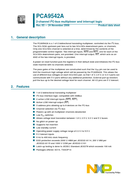
1.General descriptionThe PCA9542A is a 1-of-2 bidirectional translating multiplexer, controlled via the I 2C-bus.The SCL/SDA upstream pair fans out to two SCx/SDx downstream pairs, or channels.Only one SCx/SDx channel is selected at a time, determined by the contents of the programmable control register. Two interrupt inputs,INT0 and INT1, one for each of the SCx/SDx downstream pairs, are provided. One interrupt output,INT, which acts as an AND of the two interrupt inputs, is provided.A power-on reset function puts the registers in their default state and initializes the I 2C-bus state machine with no channels selected.The pass gates of the multiplexer are constructed such that the V DD pin can be used to limit the maximum high voltage which will be passed by the PCA9542A. This allows the use of different bus voltages on each SCx/SDx pair,so that 1.8V ,2.5V ,or 3.3V parts can communicate with 5V parts without any additional protection. External pull-up resistors pull the bus up to the desired voltage level for each channel. All I/O pins are 5V tolerant.2.FeaturesI 1-of-2 bidirectional translating multiplexerI I 2C-bus interface logic; compatible with SMBus I 2 active LOW interrupt inputs (INT0,INT1)I Active LOW interrupt output (INT)I 3 address pins allowing up to 8 devices on the I 2C-bus I Channel selection via I 2C-busI Powers up with all multiplexer channels deselected I Low R on switchesI Allows voltage level translation between 1.8V , 2.5V , 3.3V and 5V buses I No glitch on power-up I Supports hot insertion I Low standby currentI Operating power supply voltage range of 2.3V to 5.5V I 5V tolerant inputsI 0Hz to 400kHz clock frequencyIESD protection exceeds 2000V HBM per JESD22-A114, 200V MM per JESD22-A115 and 1000V CDM per JESD22-C101I Latch-up testing is done to JEDEC Standard JESD78 which exceeds 100mA I Packages offered: SO14, TSSOP14PCA9542A2-channel I 2C-bus multiplexer and interrupt logicRev. 03 — 24 November 2008Product data sheet3.Ordering information3.1Ordering options4.Block diagramTable 1.Ordering informationType numberPackage NameDescriptionVersion PCA9542AD SO14plastic small outline package; 14leads;body width 3.9mmSOT108-1PCA9542APWTSSOP14plastic thin shrink small outline package; 14leads;body width 4.4mmSOT402-1Table 2.Ordering optionsType number Topside mark Temperature range PCA9542AD PCA9542AD −40°C to +85°C PCA9542APWP A9542A−40°C to +85°CFig 1.Block diagram of PCA9542ASWITCH CONTROL LOGICPCA9542APOWER-ON RESET002aae303SD1V SS V DDI 2C-BUS CONTROLINPUT FILTERSCL SDAA0A1A2SD0SC1SC0INTERRUPT LOGICINT[1:0]INT5.Pinning information5.1Pinning5.2Pin descriptionFig 2.Pin configuration for SO14Fig 3.Pin configuration for TSSOP14PCA9542AD A0V DD A1SDA A2SCLINT0INTSD0SC1SC0SD1V SSINT1002aae3011234567810912111413PCA9542APW A0V DD A1SDA A2SCLINT0INT SD0SC1SC0SD1V SSINT1002aae3021234567810912111413Table 3.Pin descriptionSymbol Pin Description A01address input 0A12address input 1A23address input 2INT04active LOW interrupt input 0SD05serial data 0SC06serial clock 0V SS 7supply groundINT18active LOW interrupt input 1SD19serial data 1SC110serial clock 1INT 11active LOW interrupt output SCL 12serial clock line SDA 13serial data line V DD14supply voltage6.Functional descriptionRefer to Figure 1 “Block diagram of PCA9542A”.6.1Device addressingFollowing a START condition the bus master must output the address of the slave it is accessing. The address of the PCA9542A is shown in Figure 4. To conserve power, no internal pull-up resistors are incorporated on the hardware selectable address pins and they must be pulled HIGH or LOW.The last bit of the slave address defines the operation to be performed. When set to logic 1 a read is selected, while a logic 0 selects a write operation.6.2Control registerFollowing the successful acknowledgement of the slave address,the bus master will send a byte to the PCA9542A which will be stored in the control register. If multiple bytes are received by the PCA9542A,it will save the last byte received.This register can be written and read via the I 2C-bus.6.2.1Control register definitionA SCx/SDx downstream pair, or channel, is selected by the contents of the controlregister. This register is written after the PCA9542A has been addressed. The 3LSBs of the control byte are used to determine which channel is to be selected.When a channel is selected, it will become active after a STOP condition has been placed on the I 2C-bus.This ensures that all SCx/SDx lines will be in a HIGH state when the channel is made active, so that no false conditions are generated at the time of connection.Fig 4.Slave address002aab1891110A2A1A0R/Wfixedhardware selectableFig 5.Control register002aae304XXINT1INT0XB2B1B0interrupt bits (read only)channel selection bits(read/write)76543210bitenable bit6.3Interrupt handlingThe PCA9542A provides 2 interrupt inputs, one for each channel and one open-drain interrupt output. When an interrupt is generated by any device, it will be detected by the PCA9542A and the interrupt output will be driven LOW. The channel need not be active for detection of the interrupt. A bit is also set in the control byte.Bits 5:4 of the control byte correspond to channel 1, channel 0 of the PCA9542A,respectively.Therefore,if an interrupt is generated by any device connected to channel 1,the state of the interrupt inputs is loaded into the control register when a read isaccomplished. Likewise, an interrupt on any device connected to channel 0 would cause bit 4 of the control register to be set on the read. The master can then address thePCA9542A and read the contents of the control byte to determine which channel contains the device generating the interrupt. The master can then reconfigure the PCA9542A to select this channel, and locate the device generating the interrupt and clear it.It should be noted that more than one device can be providing an interrupt on a channel,so it is up to the master to ensure that all devices on a channel are interrogated for an interrupt.The interrupt inputs may be used as general purpose inputs if the interrupt function is not required.If unused, interrupt input(s) must be connected to V DD through a pull-up resistor.Remark:The two interrupts can be active at the same time.6.4Power-on resetWhen power is applied to V DD ,an internal Power-On Reset (POR)holds the PCA9542A in a reset condition until V DD has reached V POR .At this point,the reset condition is released and the PCA9542A registers and I 2C-bus state machine are initialized to their default states (all zeroes), causing all the channels to be deselected. Thereafter, V DD must be lowered below 0.2V to reset the device.Table 4.Control register: Write—channel selection; Read—channel status D7D6INT1INT0D3B2B1B0CommandX X X X X 0X X no channel selected X X X X X 100channel 0 enabled X X X X X 101channel 1 enabled X X X X X 11X no channel selected 0no channel selected;power-up default stateTable 5.Control register read — interrupt D7D6INT1INT0D3B2B1B0Command00X 0X X X X no interrupt on channel 01interrupt on channel 000XXXXXno interrupt on channel 11interrupt on channel 16.5Voltage translationThe pass gate transistors of the PCA9542A are constructed such that the V DD voltage can be used to limit the maximum voltage that will be passed from one I 2C-bus to another.Figure 6shows the voltage characteristics of the pass gate transistors (note that the graph was generated using the data specified in Section 11 “Dynamic characteristics” of this data sheet). In order for the PCA9542A to act as a voltage translator, the V o(sw) voltage should be equal to,or lower than the lowest bus voltage.For example,if the main bus was running at 5V , and the downstream buses were 3.3V and 2.7V , then V o(sw) should be equal to or below 2.7V to effectively clamp the downstream bus voltages. Looking at Figure 6, we see that V o(sw)(max) will be at 2.7V when the PCA9542A supply voltage is 3.5V or lower so the PCA9542A supply voltage could be set to 3.3V .Pull-up resistors can then be used to bring the bus voltages to their appropriate levels (see Figure 13).More Information can be found in Application Note AN262,PCA954X family of I 2C/SMBus multiplexers and switches .(1)maximum (2)typical (3)minimumFig 6.Pass gate voltage versus supply voltageV DD (V)2.05.54.53.04.0002aaa9643.02.04.05.0V o(sw)(V)1.0 3.5 5.02.5(1)(2)(3)7.Characteristics of the I 2C-busThe I 2C-bus is for 2-way,2-line communication between different ICs or modules.The two lines are a serial data line (SDA) and a serial clock line (SCL). Both lines must beconnected to a positive supply via a pull-up resistor when connected to the output stages of a device. Data transfer may be initiated only when the bus is not busy.7.1Bit transferOne data bit is transferred during each clock pulse.The data on the SDA line must remain stable during the HIGH period of the clock pulse as changes in the data line at this time will be interpreted as control signals (see Figure 7).7.2START and STOP conditionsBoth data and clock lines remain HIGH when the bus is not busy. A HIGH-to-LOWtransition of the data line while the clock is HIGH is defined as the START condition (S).A LOW-to-HIGH transition of the data line while the clock is HIGH is defined as the STOP condition (P) (see Figure 8).7.3System configurationA device generating a message is a ‘transmitter’, a device receiving is the ‘receiver’. The device that controls the message is the ‘master’ and the devices which are controlled by the master are the ‘slaves’ (see Figure 9).Fig 7.Bit transfermba607data line stable;data validchange of data allowedSDASCLFig 8.Definition of START and STOP conditionsmba608SDA SCLPSTOP conditionSDASCLSSTART condition7.4AcknowledgeThe number of data bytes transferred between the START and the STOP conditions from transmitter to receiver is not limited. Each byte of eight bits is followed by oneacknowledge bit. The acknowledge bit is a HIGH level put on the bus by the transmitter,whereas the master generates an extra acknowledge related clock pulse.A slave receiver which is addressed must generate an acknowledge after the reception of each byte.Also,a master must generate an acknowledge after the reception of each byte that has been clocked out of the slave transmitter. The device that acknowledges has to pull down the SDA line during the acknowledge clock pulse so that the SDA line is stable LOW during the HIGH period of the acknowledge related clock pulse; setup and hold times must be taken into account.A master receiver must signal an end of data to the transmitter by not generating an acknowledge on the last byte that has been clocked out of the slave. In this event, the transmitter must leave the data line HIGH to enable the master to generate a STOP condition.Fig 9.System configuration002aaa966MASTER TRANSMITTER/RECEIVERSLAVE RECEIVERSLAVETRANSMITTER/RECEIVERMASTER TRANSMITTERMASTER TRANSMITTER/RECEIVERSDA SCLI 2C-BUS MULTIPLEXERSLAVEFig 10.Acknowledgement on the I 2C-bus002aaa987S START condition9821clock pulse for acknowledgementnot acknowledgeacknowledgedata output by transmitterdata output by receiverSCL from master7.5Bus transactions8.Application design-in informationFig 11.Write control registerFig 12.Read control register002aae299XXXXXB2B1B011A2A1A0AS1APslave addressSTART condition R/Wacknowledge from slave acknowledge from slave control registerSDASTOP condition002aae305XXINT 1INT 0XB2B1B011A2A1A01AS1NA Pslave addressSTART condition R/Wacknowledgefrom slave no acknowledgefrom mastercontrol register SDASTOP conditionlast byte(1)If the device generating the interrupt has an open-drain output structure or can be 3-stated,a pull-up resistor is required.If the device generating the interrupt has a totem pole output structure and cannot be 3-stated,a pull-up resistor is not required.The interrupt inputs should not be left floating.Fig 13.Typical applicationPCA9542ASD0SC0A1A0V SSSDA SCL INTV DD = 3.3 VV DD = 2.7 V to 5.5 VI 2C-bus/SMBus master002aae306SDA SCLchannel 0V = 2.7 V to 5.5 VA2INT0(1)SD1SC1channel 1V = 2.7 V to 5.5 VINT1(1)9.Limiting valuesTable 6.Limiting valuesIn accordance with the Absolute Maximum Rating System (IEC 60134).Voltages are referenced to ground (V SS = 0V).[1]Symbol Parameter Conditions Min Max UnitV DD supply voltage−0.5+7.0VV I input voltage−0.5+7.0VI I input current-±20mAI O output current-±25mAI DD supply current-±100mAI SS ground supply current-±100mAP tot total power dissipation-400mWT stg storage temperature−60+150°CT amb ambient temperature operating−40+85°C[1]The performance capability of a high-performance integrated circuit in conjunction with its thermalenvironment can create junction temperatures which are detrimental to reliability. The maximum junctiontemperature of this integrated circuit should not exceed 125°C.10.Static characteristics[1]For operation between published voltage ranges, refer to worst case parameter in both ranges.[2]V DD must be lowered to 0.2V in order to reset part.Table 7.Static characteristicsV DD =2.3V to 3.6V ; V SS =0V; T amb =−40°C to +85°C; unless otherwise specified.See Table 8 for V DD =4.5V to 5.5V .[1]Symbol Parameter Conditions Min Typ Max Unit Supply V DD supply voltage 2.3- 3.6V I DDsupply currentoperating mode; V DD =3.6V;no load; V I =V DD or V SS ;f SCL =100kHz-1030µAI stb standby current standby mode; V DD =3.6V; no load;V I =V DD or V SS ; f SCL =0kHz -0.11µA V POR power-on reset voltage no load; V I =V DD or V SS[2]- 1.6 2.1V Input SCL; input/output SDAV IL LOW-level input voltage −0.5-+0.3V DD V V IH HIGH-level input voltage 0.7V DD-6V I OL LOW-level output current V OL =0.4V 37-mA V OL =0.6V 610-mA I L leakage current V I =V DD or V SS −1-+1µA C i input capacitance V I =V SS-910pF Select inputs A0, A1, A2,INT0,INT1V IL LOW-level input voltage −0.5-+0.3V DD V V IH HIGH-level input voltage 0.7V DD-V DD +0.5V I LI input leakage current V I =V DD or V SS −1-+1µA C iinput capacitance V I =V SS- 1.63pF Pass gate R onON-state resistanceV DD =3.0V to 3.6V; V O =0.4V;I O =15mA51130ΩV DD =2.3V to 2.7V; V O =0.4V;I O =10mA71655ΩV o(sw)switch output voltageV i(sw)=V DD =3.3V; I o(sw)=−100µA - 1.9-V V i(sw)=V DD =3.0V to 3.6V;I o(sw)=−100µA1.6-2.8V V i(sw)=V DD =2.5V; I o(sw)=−100µA - 1.5-V V i(sw)=V DD =2.3V to 2.7V;I o(sw)=−100µA1.1-2.0V I L leakage current V I =V DD or V SS −1-+1µA C ioinput/output capacitance V I =V SS -35pF INT output I OL LOW-level output current V OL =0.4V3--mA I OHHIGH-level output current--+10µA[1]For operation between published voltage ranges, refer to worst case parameter in both ranges.[2]V DD must be lowered to 0.2V in order to reset part.Table 8.Static characteristicsV DD =4.5V to 5.5V ; V SS =0V; T amb =−40°C to +85°C; unless otherwise specified.See Table 7 for V DD =2.3V to 3.6V .[1]Symbol Parameter Conditions Min Typ Max Unit Supply V DD supply voltage 4.5- 5.5V I DDsupply currentoperating mode; V DD =5.5V;no load; V I =V DD or V SS ;f SCL =100kHz-25100µAI stb standby current standby mode; V DD =5.5V; no load;V I =V DD or V SS ; f SCL =0kHz -0.31µA V POR power-on reset voltage no load; V I =V DD or V SS[2]- 1.7 2.1V Input SCL; input/output SDAV IL LOW-level input voltage −0.5-+0.3V DD V V IH HIGH-level input voltage 0.7V DD-6V I OL LOW-level output current V OL =0.4V 3--mA V OL =0.6V 6--mA I L leakage current V I =V DD or V SS −1-+1µA C i input capacitance V I =V SS-910pF Select inputs A0, A1, A2,INT0,INT1V IL LOW-level input voltage −0.5-+0.3V DD V V IH HIGH-level input voltage 0.7V DD-V DD +0.5V I LI input leakage current V I =V DD or V SS −1-+1µA C iinput capacitance V I =V SS-25pF Pass gate R on ON-state resistance V DD =4.5V to 5.5V; V O =0.4V;I O =15mA4924ΩV o(sw)switch output voltageV i(sw)=V DD =5.0V; I o(sw)=−100µA - 3.6-V V i(sw)=V DD =4.5V to 5.5V;I o(sw)=−100µA2.6- 4.5V I L leakage current V I =V DD or V SS −1-+1µA C ioinput/output capacitance V I =V SS -35pF INT output I OL LOW-level output current V OL =0.4V3--mA I OHHIGH-level output current--+10µA11.Dynamic characteristics[1]Pass gate propagation delay is calculated from the 20Ω typical R on and the 15pF load capacitance.[2]After this period, the first clock pulse is generated.[3] A device must internally provide a hold time of at least 300ns for the SDA signal (referred to the V IH(min) of the SCL signal) in order to bridge the undefined region of the falling edge of SCL.[4]C b =total capacitance of one bus line in pF .[5]Measurements taken with 1k Ω pull-up resistor and 50pF load.Table 9.Dynamic characteristics SymbolParameterConditionsStandard-modeI 2C-bus Fast-mode I 2C-busUnitMinMax Min Max t PD propagation delay from SDA to SDn,or SCL to SCn-0.3[1]-0.3[1]ns f SCL SCL clock frequency01000400kHz t BUF bus free time between a STOP and ST ART condition4.7- 1.3-µs t HD;STA hold time (repeated) ST ART condition[2]4.0-0.6-µs t LOW LOW period of the SCL clock 4.7- 1.3-µs t HIGH HIGH period of the SCL clock 4.0-0.6-µs t SU;ST A set-up time for a repeated ST ART condition4.7-0.6-µs t SU;STO set-up time for STOP condition 4.0-0.6-µs t HD;DA T data hold time 0[3] 3.450[3]0.9µs t SU;DA T data set-up time250-100-ns t r rise time of both SDA and SCL signals-100020+0.1C b [4]300ns t f fall time of both SDA and SCL signals-30020+0.1C b [4]300µs C b capacitive load for each bus line -400-400µs t SP pulse width of spikes that must be suppressed by the input filter -50-50ns t VD;DA T data valid timeHIGH-to-LOW [5]-1-1µs LOW-to-HIGH[5]-0.6-0.6µs t VD;ACK data valid acknowledge time-1-1µs INTt v(INTnN-INTN)valid time from INTn to INT signal [5]-4-4µs t d(INTnN-INTN)delay time from INTn to INT inactive [5]-2-2µs t w(rej)L LOW-level rejection time INTn inputs [5]1-1-µs t w(rej)HHIGH-level rejection timeINTn inputs[5]0.5-0.5-µsFig 14.Definition of timing on the I 2C-bust SPt BUFt HD;STAPPSt LOWt rt HD;DAT t ft HIGH t SU;DATt SU;STASrt HD;STAt SU;STOSDASCL002aaa98612.Package outlineFig 15.Package outline SOT108-1 (SO14)UNIT Amax.A 1A 2A 3b p c D (1)E (1)(1)e H E L L p Q Z y w v θREFERENCESOUTLINE VERSION EUROPEAN PROJECTIONISSUE DATE IEC JEDEC JEITAmminches 1.750.250.101.451.250.250.490.360.250.198.758.554.03.8 1.27 6.25.80.70.60.70.38oo 0.250.1DIMENSIONS (inch dimensions are derived from the original mm dimensions)Note1. Plastic or metal protrusions of 0.15 mm (0.006 inch) maximum per side are not included.1.00.4SOT108-1Xw MθAA 1A 2b pD H EL pQdetail XE Z ecL v M A(A )3A78114y076E06MS-012pin 1 index0.0690.0100.0040.0570.0490.010.0190.0140.01000.00750.350.340.160.150.051.050.0410.2440.2280.0280.0240.0280.0120.010.250.010.0040.0390.01699-12-2703-02-190 2.5 5 mmscaleSO14: plastic small outline package; 14 leads; body width 3.9 mmSOT108-1Fig 16.Package outline SOT402-1 (TSSOP14)UNIT A 1A 2A 3b p c D (1)E (2)(1)e H E L L p Q Z y w v θ REFERENCESOUTLINE VERSION EUROPEAN PROJECTIONISSUE DATE IECJEDEC JEITAmm0.150.050.950.800.300.190.20.15.14.94.54.30.656.66.20.40.30.720.3880oo 0.130.10.21DIMENSIONS (mm are the original dimensions)Notes1. Plastic or metal protrusions of 0.15 mm maximum per side are not included.2. Plastic interlead protrusions of 0.25 mm maximum per side are not included.0.750.50SOT402-1MO-15399-12-2703-02-18w Mb pD Ze0.2517148θAA 1A 2L p Qdetail XL(A )3H EE cv M AXAy0 2.5 5 mmscaleTSSOP14: plastic thin shrink small outline package; 14 leads; body width 4.4 mm SOT402-1Amax.1.1pin 1 index13.Soldering of SMD packagesThis text provides a very brief insight into a complex technology.A more in-depth accountof soldering ICs can be found in Application Note AN10365 “Surface mount reflowsoldering description”.13.1Introduction to solderingSoldering is one of the most common methods through which packages are attached toPrinted Circuit Boards(PCBs),to form electrical circuits.The soldered joint provides boththe mechanical and the electrical connection. There is no single soldering method that isideal for all IC packages. Wave soldering is often preferred when through-hole andSurface Mount Devices (SMDs) are mixed on one printed wiring board; however, it is notsuitable for fine pitch SMDs. Reflow soldering is ideal for the small pitches and highdensities that come with increased miniaturization.13.2Wave and reflow solderingWave soldering is a joining technology in which the joints are made by solder coming froma standing wave of liquid solder. The wave soldering process is suitable for the following:•Through-hole components•Leaded or leadless SMDs, which are glued to the surface of the printed circuit boardNot all SMDs can be wave soldered. Packages with solder balls, and some leadlesspackages which have solder lands underneath the body, cannot be wave soldered. Also,leaded SMDs with leads having a pitch smaller than ~0.6mm cannot be wave soldered,due to an increased probability of bridging.The reflow soldering process involves applying solder paste to a board, followed bycomponent placement and exposure to a temperature profile. Leaded packages,packages with solder balls, and leadless packages are all reflow solderable.Key characteristics in both wave and reflow soldering are:•Board specifications, including the board finish, solder masks and vias•Package footprints, including solder thieves and orientation•The moisture sensitivity level of the packages•Package placement•Inspection and repair•Lead-free soldering versus SnPb soldering13.3Wave solderingKey characteristics in wave soldering are:•Process issues, such as application of adhesive and flux, clinching of leads, boardtransport, the solder wave parameters, and the time during which components areexposed to the wave•Solder bath specifications, including temperature and impurities13.4Reflow solderingKey characteristics in reflow soldering are:•Lead-free versus SnPb soldering;note that a lead-free reflow process usually leads to higher minimum peak temperatures (see Figure17) than a SnPb process, thusreducing the process window•Solder paste printing issues including smearing, release, and adjusting the process window for a mix of large and small components on one board•Reflow temperature profile; this profile includes preheat, reflow (in which the board is heated to the peak temperature) and cooling down. It is imperative that the peaktemperature is high enough for the solder to make reliable solder joints(a solder pastecharacteristic). In addition, the peak temperature must be low enough that thepackages and/or boards are not damaged. The peak temperature of the packagedepends on package thickness and volume and is classified in accordance withTable10 and11Table 10.SnPb eutectic process (from J-STD-020C)Package thickness (mm)Package reflow temperature (°C)Volume (mm3)< 350≥ 350< 2.5235220≥ 2.5220220Table 11.Lead-free process (from J-STD-020C)Package thickness (mm)Package reflow temperature (°C)Volume (mm3)< 350350 to 2000> 2000 < 1.62602602601.6 to2.5260250245> 2.5250245245Moisture sensitivity precautions, as indicated on the packing, must be respected at alltimes.Studies have shown that small packages reach higher temperatures during reflowsoldering, see Figure17.For further information on temperature profiles, refer to Application Note AN10365“Surface mount reflow soldering description”.14.AbbreviationsMSL: Moisture Sensitivity LevelFig 17.Temperature profiles for large and small components001aac844temperaturetimeminimum peak temperature = minimum soldering temperaturemaximum peak temperature = MSL limit, damage levelpeak temperatureTable 12.AbbreviationsAcronym DescriptionCDM Charged-Device Model ESD ElectroStatic Discharge HBM Human Body Model I/O Input/OutputI 2C-bus Inter-Integrated Circuit bus LSB Least Significant Bit MM Machine Model POR Power-On ResetSMBusSystem Management Bus15.Revision historyTable 13.Revision historyDocument ID Release date Data sheet status Change notice SupersedesPCA9542A_320081124Product data sheet-PCA9542A_2Modifications:•The format of this data sheet has been redesigned to comply with the new identity guidelines of NXP Semiconductors.•Legal texts have been adapted to the new company name where appropriate.•Section 2 “Features”:–8th bullet item: changed from “Rds ON” to “R on”–16th bullet item: changed from “and 1000V per JESD22-C101” to “and 1000V CDM perJESD22-C101”•Section 5.1 “Pinning”: added separate pinning diagrams for SO14 and TSSOP14•Section 6.5 “Voltage translation”: changed symbol from “V pass” to “V o(sw)”•Table 6 “Limiting values”:–changed parameter for I SS from “supply current” to “ground supply current”–changed parameter for T amb from “operating ambient temperature” to “ambient temperature”(moved “operating” to Conditions column)–deleted (old) table note 1 (this statement is now located in Section 16.3 “Disclaimers”,paragraph “Limiting values”)–Table note [1], 2nd sentence: changed from “should not exceed 150°C” to “should not exceed 125°C”•Table 7 “Static characteristics” (V DD=2.3V to 3.6V):–table title changed from “DC characteristics” to “Static characteristics”–sub-section “Pass gate”: changed symbol/parameter from “R ON, Switch resistance” to“R on,ON-state resistance”–sub-section “Pass gate”: changed symbol from “V Pass” to “V o(sw)”–sub-section “Pass gate”, Conditions column: changed symbol from “V swin” to “V i(sw)”;changed symbol from “I swout” to “I o(sw)”•Table 8 “Static characteristics” (V DD=4.5V to 5.5V):–table title changed from “DC characteristics” to “Static characteristics”–sub-section “Pass gate”: changed symbol/parameter from “R ON, Switch resistance” to“R on,ON-state resistance”–sub-section “Pass gate”: changed symbol from “V Pass” to “V o(sw)”–sub-section “Pass gate”, Conditions column: changed symbol from “V swin” to “V i(sw)”;changed symbol from “I swout” to “I o(sw)”•Table 9 “Dynamic characteristics”:–symbol t HD;STA:phrase“After this period,thefirst clock pulse is generated.”has been moved to Table note [2]–symbols t VD:DA TL and t VD:DATH merged to form t VD;DA T (and added Conditions “HIGH-to-LOW”and “LOW-to-HIGH”)–sub-section “INT” re-written in its entirety•Added soldering information•Added Section 14 “Abbreviations”PCA9542A_220040929Product data sheet-PCA9542A_1 (939775013955)20040727Objective data sheet--PCA9542A_1(939775013307)。
波农高性能功率测量仪型号参数规格书说明书

Net RF Power absorbed by sensor
Thermocouples Diode Detectors
Power Meter
Power sensor
Substituted DC or low frequency
equivalent
Fig 1: Typical block diagram for direct power measurement. The RF source can be any RF signal attached to the power sensor. Three different types of sensors are available based on
Calibration and Traceability Boonton employs both a linearity calibration as well as a frequency response calibration. This maximizes the performance of Diode Sensors and corrects non-linearity on all ranges. Linearity calibration can be used to extend the operating range of a Diode Sensor. It can also be used to correct non-linearity throughout a Thermocouple or Diode sensor’s dynamic range. Frequency calibration factors (NIST traceable) and other data are stored within all peak power sensors. Linearity calibration is performed using the peak power meter’s built-in calibrator.
广州致远电子 PCA9548AB AD APW IC 多路复用器和开关 产品数据手册
PCA9548AB/AD/APW2广州致远电子有限公司类别内容关键词 PCA9548A 、多路复用器、开关摘 要 PCA9548A 是一款通过I 2C 总线控制的八进制双向转换开关1. 概述PCA9548A是一款通过I2C总线控制的八进制双向转换开关。
它的每对SCL/ SDA上行通道可以扩展为八对下行通道,可以通过可编程控制寄存器的内容来选择任意单一的SCx/SDx通道或者组合通道。
由多路复用器的通门,V DD管脚可以用来限制PCA9547通过的最高电压,这使得每一对SCL/SDA都可以使用不同的总线电压,因此1.8V、2.5V或3.3V 的器件可以在无其它保护的情况下与5V的器件进行通信。
它的外部上拉电阻将总线拉高至每个通道所要求的电压电平,所有I/O管脚都可以承受5V电压。
当一次低有效的电压复位输入时,会使得PCA9548A能恢复到下行I2C总线处于低电平的状态。
就像内部上电复位的功能一样,复位引脚拉低会复位I2C总线并且禁止所有的通道。
2. 特征8路双向转换开关;I2C总线逻辑接口,兼容的SMBus标准;低电压输入复位;3地址引脚允许I2C总线连接多达8个设备;在任意组合中,可以通过I2C总线选择通道;上电时所有开关通道被禁止;低导通电阻的多路复用器;转换器允许总线电压在1.8V,2.5V,3.3V和5V的电平之间转换;上电时无干扰脉冲信号;支持热插拔;待机电流更低;电源电压运行时范围为2.3V至5.5V ;5伏宽压输入;0 Hz到400 kHz的时钟频率;ESD 保护:JESD22-A114 为2000V HBM,JESD22-A115 为200V 和JESD22-C101 为1000V CDM ;超过100mA 的JESDEC 标准JESD78 要进行栓锁测试(Latch-up testing);三种封装形式:SO24 ,TSSOP24和HVQFN24。
3. 订购信息3.1 订购信息器件的相关信息如表3.1所示:表3.1 器件的相关信息封装产品型号名称说明版本PCA9548ABS HVQFN24热增强型超薄四方扁平塑料封装;无引脚;24端子;大小为4×4×0.85mmSOT616-1PCA9548AD SO24小外形塑料封装;24个引脚;宽度为7.5mmSOT137-1PCA9548APW TSSOP24 小外形薄体收缩型塑料封装;24个引脚;宽度为4.4mmSOT355-13.2 订购选择器件选型的相关参数如表3.2所示:表3.2 器件选型参数产品型号顶层标号温度范围PCA9548ABS 548A -40 ℃ to +85 ℃PCA9548AD PCA9548AD -40 ℃ to +85 ℃PCA9548APW PCA9548A -40 ℃ to +85 ℃4. 内部结构框图PCA9548A的内部结构框图如图4.1所示:图4.1 PCA9548A的内部结构框图5. 引脚信息5.1 引脚图SO24封装形式的引脚配置如图5.1所示:图5.1 PCA9548AD引脚配置图TSSOP24封装形式的引脚配置如图5.2所示:图5.2 PCA9548APW引脚配置图HVQFN封装形式的引脚配置如图5.3所示:图5.3 PCA9548ABS引脚配置图5.2 引脚说明各个封装类型的引脚说明如表5.1所示:表5.1 引脚说明SD2 8SC2 9SD3 10续上表引脚说明标号SO,TSSOP HVQFNSD5 15 12 串行数据5SC5 16 13 串行时钟5SD6 17 14 串行数据6SC6 18 15 串行时钟6SD7 19 16 串行数据7SC7 20 17 串行时钟7A2 21 18 地址2输入SCL 22 19 串行时钟线SDA 23 20 串行数据线V DD 24 21 电源信号[1]HVQFN封装的地信号连接到V SS引脚和裸露焊盘中心。
jbt9542电动机标准
jbt9542电动机标准
在JBT9542标准中,通常会包括电动机的分类、技术要求、试验方法、检验规则等内容。
具体涉及到电动机的额定参数、外观质量、绝缘性能、温升、效率、功率因数、起动性能、转矩与转速特性、噪声和振动等方面的要求。
此外,标准还可能包括了对电动机的包装、运输和储存的要求,以及标识、说明书等方面的规定。
对于生产厂家来说,遵循JBT9542标准意味着他们的产品符合国家规定的质量标准,有助于提升产品竞争力,增强消费者信心。
对于用户来说,选择符合JBT9542标准的电动机意味着其产品质量有一定的保障,能够满足相关的技术要求,有利于提高设备的可靠性和稳定性。
总的来说,JBT9542作为电动机的标准,对于规范行业发展、保障产品质量、提高能源利用效率都具有重要意义。
因此,生产企业和用户都应该重视并遵循这一标准,以推动电动机行业的可持续发展。
tca9548a使用手册
tca9548a使用手册TCA9548A是一款I2C多路复用器,它可以让您通过单个I2C总线连接多个I2C设备。
以下是关于TCA9548A的使用手册:1. 硬件连接,首先,您需要将TCA9548A连接到您的主控制器(如Arduino、Raspberry Pi等)的I2C总线上。
确保正确连接TCA9548A的电源和地线引脚,并将SCL和SDA引脚连接到主控制器的对应引脚上。
2. 地址设置,TCA9548A具有3个地址引脚(A0、A1和A2),您可以通过连接这些引脚来设置TCA9548A的I2C地址。
根据您的需求,设置TCA9548A的地址以避免与其他I2C设备地址冲突。
3. 控制通道,TCA9548A可以控制8个独立的I2C通道,通过设置寄存器来选择要与主控制器通信的通道。
您可以使用相应的库或驱动程序来编程控制TCA9548A,以便选择特定的通道和与连接到该通道的设备进行通信。
4. 设置时序,在使用TCA9548A时,您需要注意时序的设置,确保在切换通道时给足够的时间让设备稳定。
此外,还要注意主控制器和TCA9548A之间的通信时序,以确保数据的正确传输。
5. 设备接入,一旦设置好TCA9548A,您可以将多个I2C设备连接到TCA9548A的各个通道上。
确保每个设备的地址不会与其他设备冲突,并根据需要编写相应的控制代码来与这些设备进行通信。
总之,TCA9548A是一款强大的I2C多路复用器,可以帮助您简化多个I2C设备的连接和控制。
通过正确的硬件连接、地址设置、通道控制和设备接入,您可以充分发挥TCA9548A的功能,实现对多个I2C设备的灵活控制和管理。
希望这些信息对您有所帮助。
扩展频谱式雷达设备[发明专利]
![扩展频谱式雷达设备[发明专利]](https://img.taocdn.com/s3/m/1e8b10e290c69ec3d4bb751b.png)
专利名称:扩展频谱式雷达设备专利类型:发明专利
发明人:福田健志
申请号:CN200680010220.6申请日:20060329
公开号:CN101151551A
公开日:
20080326
专利内容由知识产权出版社提供
摘要:扩展频谱式雷达设备(100)将第一振荡信号、第二振荡信号以及发送用伪噪声码相互组合,进行扩展频谱来产生扩展信号,其中包括:发送部(101),其将扩展信号作为探测用电波发射;以及接收部(102),其将由物体反射来的探测用电波作为接收信号接收,并利用接收用伪噪声码即推迟一段时间来提供的发送用伪噪声码和第一振荡信号来对接收信号进行逆扩展,从而产生中频信号。
申请人:松下电器产业株式会社
地址:日本大阪府
国籍:JP
代理机构:永新专利商标代理有限公司
代理人:黄剑锋
更多信息请下载全文后查看。
- 1、下载文档前请自行甄别文档内容的完整性,平台不提供额外的编辑、内容补充、找答案等附加服务。
- 2、"仅部分预览"的文档,不可在线预览部分如存在完整性等问题,可反馈申请退款(可完整预览的文档不适用该条件!)。
- 3、如文档侵犯您的权益,请联系客服反馈,我们会尽快为您处理(人工客服工作时间:9:00-18:30)。
元器件交易网
SO14:plastic small outline package; 14 leads; body width 3.9 mm SOT108-1
TSSOP14:plastic thin shrink small outline package; 14 leads; body width 4.4 mm SOT402-1
Definitions
Short-form specification — The data in a short-form specification is extracted from a full data sheet with the same type number and title. For detailed information see the relevant data sheet or data handbook.
Limiting values definition — Limiting values given are in accordance with the Absolute Maximum Rating System (IEC 60134). Stress above one or more of the limiting values may cause permanent damage to the device. These are stress ratings only and operation of the device at these or at any other conditions above those given in the Characteristics sections of the specification is not implied. Exposure to limiting values for extended periods may affect device reliability.
Application information — Applications that are described herein for any of these products are for illustrative purposes only. Philips Semiconductors make no representation or warranty that such applications will be suitable for the specified use without further testing or modification.
Disclaimers
Life support — These products are not designed for use in life support appliances, devices, or systems where malfunction of these products can reasonably be expected to result in personal injury. Philips Semiconductors customers using or selling these products for use in such applications do so at their own risk and agree to fully indemnify Philips Semiconductors for any damages resulting from such application.
Right to make changes — Philips Semiconductors reserves the right to make changes in the products—including circuits, standard cells, and/or software—described or contained herein in order to improve design and/or performance. When the product is in full production (status ‘Production’), relevant changes will be communicated via a Customer Product/Process Change Notification (CPCN). Philips Semiconductors assumes no responsibility or liability for the use of any of these products, conveys no license or title under any patent, copyright, or mask work right to these products, and makes no representations or warranties that these products are free from patent, copyright, or mask work right infringement, unless otherwise specified.
Contact information
For additional information please visit
.Fax: +31 40 27 24825
For sales offices addresses send e-mail to:
© Koninklijke Philips Electronics N.V. 2004
All rights reserved. Published in the U.S.A.
Date of release: 09-04
Document number:9397 750 13955。