BSC079N10NS G中文资料
中国联通移动网诺基亚bsc设备维护操作手册
中国联通移动网诺西设备 诺西 C 操作维护手册
中国联通移动网诺西维护技术基地
1
中国联通移动网诺基亚 BSC 操作维护手册
目录
1 系统结构及重要硬件介绍 ...................................................................5
2
中国联通移动网诺基亚 BSC 操作维护手册
5.1.2 问题分析 ............................................................................85 5.1.3 问题处理 ............................................................................87 5.1.4 总结 ................................................................................87 5.2 2725 告警处理 .........................................................................87 5.2.1 问题及告警描述 ......................................................................87 5.2.2 问题分析 ............................................................................88 5.2.3 问题处理 .....................................
海外规格仕样书第4版(中文)
4.在机铭板上标示出以下内容 ・制造者名 ・制造年月 ・形式以及model编号 ・定格电源电压(电压、位相、周波数、最大负荷电流、etc) 在电源上不可以用「AC200V」表示,而要用「~200V」表示 ・气压(定格压力) ・原产地表示(MADE IN JAPAN等) 注)FA标准机铭板: 4—710—156—01(大—11) 带孔、by三立产业 EN60204 UL1740
8.盖子、马达框架、trans core、电装品筐体、以及接续管等的金属部, 如果和地线或金属接触,会导致和物品本身的导通。
EN60204、UL1740
7/28
要求事项
1.电源切断装置要使用得到认可的漏电断路器、自动断路器、线路保护器 EN60204、UL1740 2.主断路器的定格要遵循以下事项。 EN60204、UL1740 a)电流容量:最大负荷电流的115%以上,或者使用的导线的要求容许电流以下 (14配线以及电路——参照17) b)切断容量:在机器上使用的马达中,最大马达的 rotor rock电流+其他装置的 最大负荷电流以上 3.电力引入线(一次电源)要直接和断路器连接 EN60204、UL1740 4.电源切断装置遵循一下事项。 EN60204、UL1740 (a)安装把手,方便从外部操作 (b)把手的中心高度在0.6~1.9以内 (c)要有OFF锁定机能.(可以上锁的构造) (d)门关上时要有ON/OFF的明确指示 (e)ON/OFF可以用「O」也可以用「I」来表示 (f)接地导线以外所有的相要同时切断 (g)主断路器上如果没有OFF锁定机能,要在负荷侧设定带钥匙的主开关。
贵社 check
本社 check
备注
① 外 观 以 及 构 造 的 规 定
4/28
BSC介绍

BIE框
主控框(上框) 主控框(下框)
BM机柜配置
BM的主控框
0 1
2 3 4 5 6 7 8
9 10
11 12
13 14
15 16 17 18 19 20 21 22 23
24 25
P W C P W C
N N N O O O D D D
E M A
M P U M P U
N
E T
N E
L P N 7 L A P D
主机程序和数据的加载路径:
Flash Memory DRAM
程 序 数 据 C P U
由BAM直接向DRAM中加载程序和数 据; 由Flash Memory向DRAM中加载程序 和数据。
程序
MPU
数据
BAM
MPU开关
MPU板正面有2个拨码开 关: S1(8位拨码开关); S2(4位拨码开关)。
MPU开关——S1
SNT信令交换网板 完成各模块间控制信号和内信息的交换,并 提供主机向各个模块加载的通道,2块SNT 互为主备用
ALM告警板 负责各种机架内告警信号的采集与告警灯 的驱动输出
传输接口框
0 2 3 4 5 6 7 8 9 1 1 1 1 1 1 1 1 2 2 2 2 2 1 0 1 3 5 6 7 8 9 0 1 2 3 4 1 1 2 4 上 P E E E E E E E E 框 W 3 3 3 3 3 3 3 3 C M M M M M M M M 2 5 E E E E E E E E P 3 3 3 3 3 3 3 3 W M M M M M M M M C
CTN中心交换网板
CTN是AM/CM的中心话路交换系统 CTN占 2个槽位,跨2个机框 2块 CTN 互为主备用
【优质文档】nsn资料-推荐word版 (25页)

本文部分内容来自网络整理,本司不为其真实性负责,如有异议或侵权请及时联系,本司将立即删除!== 本文为word格式,下载后可方便编辑和修改! ==nsn资料篇一:NSN LTE产品介绍与配套中国电信4G试验工程无线网基站产品介绍与配套方案诺基亚西门子通信技术(北京)有限公司诺基亚西门子通信网络科技服务有限公司201X年9月目录一、BBU系统模块结构 .................................................................. ................................................... 3 1. 2. 3. 4.FSMF主控系统模块 .................................................................. .................................................. 3 FBBA基带扩展子模块 .................................................................. .............................................. 5 FTIF传输扩展子模块 .................................................................. ................................................ 5 FPFD电源扩展子模块 .................................................................. . (6)二、BBU系统模块电器配套规格 .................................................................. .................................... 7 三、BBU系统模块安装方式 .................................................................. ............................................ 8 1.FCIA室内机柜安装(宏基站模型) ................................................................ ............................ 8 2.EMHA+FMCF防尘壳安装(BBU+RRU模型) ................................................................ ............. 9 四、BBU系统模块处理能力 ............................................................................................................ 10 1.FDD系统处理能力 .................................................................. .................................................... 10 2.TDD系统处理能力 .................................................................. .................................................... 11 五、RRU射频模块 .................................................................. ......................................................... 12 1. FDD RRU射频模块对标 .................................................................. ............................................ 12 2.TDD RRU射频模块对标 .................................................................. ............................................ 13 3. FDD RRU射频模块电器配套规格................................................................... ............................ 14 4. FDD RRU射频模块电器配套规格................................................................... ............................ 16 六、BBU+RRU典型配置示例说明 .................................................................. .................................. 17 1. FDD BBU+RRU典型配置 .................................................................. ........................................... 17 2. TDD BBU+RRU典型配置 .................................................................. ........................................... 18 七、网管系统 .................................................................. ................................................................ 19 1. 诺西网管NETACT介绍 .................................................................. ............................................... 19 2. 网管电器配套规格 .................................................................. . (22)一、BBU系统模块结构TDD/FDD-LTE BBU 采用诺基亚西门子最新的Flexi Multiradio BBU,支持2G/WCDMA/LTE等多制式的共平台演进。
ProductTypeList-optiMOS(20-250V)

N-Channel MOSFETs: OptiMOS™ (20V…250V) Product TypeProduct TypeBSN045NE2LSBSN011NE2LSBSN011NE2LSIBSN012N03LSBSN012N03LSIBSN048N03LSBSB012NE2LXBSB014N04LX3 GBSB015N04NX3 GBSB017N03LX3 GBSB012N03LX3 GBSB028N06NN3 GBSB044N08NN3 GBSB056N10NN3 GBSB013NE2LXIBSB008NE2LXBSB280N15NZ3 G BSB165N15NZ3 G BSB012NE2LXI BSF024N03LT3 G BSF050N03LQ3 G BSF030NE2LQ BSF134N10NJ3 G BSF110N06NT3 G BSF450NE7NH3 G BSF035NE2LQ IPB015N04L G IPB027N10N3 G IPB035N08N3 G IPB015N04N G IPB019N06L3 G IPB083N10N3 G IPB042N10N3 G IPB054N06N3 GIPB037N06N3 G IPB097N08N3 G IPB055N03L G IPB054N08N3 G IPB042N03L G IPB022N04L G IPB065N03L G IPB072N15N3 G IPB025N08N3 G IPB080N03L G IPB081N06L3 G IPB147N03L G IPB096N03L G IPB136N08N3 GIPB090N06N3 G IPB029N06N3 G IPB049NE7N3 G IPB031NE7N3 G IPB020NE7N3 G IPB123N10N3 G IPB038N12N3 G IPB144N12N3 G IPB320N20N3 G IPB107N20N3 G IPB200N25N3 G IPB600N25N3 G BUZ32 H3045A BUZ31 H3045A IPB108N15N3 G BUZ30A H3045AIPB107N20NA IPB057N06N IPB026N06N IPB230N06L3 G IPB067N08N3 G IPB034N03L G IPB009N03L G IPB011N04L G IPB011N04N G IPB016N06L3 G IPB017N06N3 G IPB019N08N3 G IPB020N04N G IPB025N10N3 G IPB030N08N3 GIPB036N12N3 G IPB065N15N3 G IPB010N06NIPB014N06NSPD07N20 GIPD031N06L3 G IPD034N06N3 G IPD035N06L3 G IPD036N04L GIPD038N06N3 G IPD048N06L3 G IPD053N08N3 G SPD50N03S2L-06 G SPD30N03S2L-07 G IPD068N10N3 G SPD50N03S2-07 GIPD082N10N3 G IPD088N06N3 G IPD096N08N3 G SPD30N03S2L-10 G IPD127N06L GIPD135N08N3 G IPD160N04L GIPD170N04N GIPD200N15N3 G SPD30N03S2L-20 G IPD220N06L3 G IPD25CN10N GIPD250N06N3 G IPD33CN10N GIPD350N06L GIPD640N06L G IPD78CN10N G IPD800N06N G IPD122N10N3 G IPD180N10N3 G IPD110N12N3 G IPD031N03L G IPD040N03L G IPD050N03L G IPD060N03L G IPD075N03L G IPD090N03L G IPD320N20N3 G IPD600N25N3 G IPD530N15N3 G IPD105N03L G IPD135N03L GIPD025N06N IPD053N06N IPI023NE7N3 G IPI034NE7N3 G IPI052NE7N3 G IPI126N10N3 G IPI180N10N3 G IPI041N12N3 G IPI076N12N3 G IPI147N12N3 G IPI045N10N3 G IPI086N10N3 G IPI030N10N3 G IPI04CN10N G IPI072N10N3 G IPI26CN10N G IPI35CN10N GIPI075N15N3 G IPI200N15N3 G IPI024N06N3 G IPI032N06N3 G IPI040N06N3 G IPI037N08N3 G IPI320N20N3 G IPI110N20N3 G IPI200N25N3 G IPI600N25N3 G IPI111N15N3 G IPI530N15N3 G IPI020N06NIPI029N06N BUZ31 H3046 IPI084N06L3 GIPU135N08N3 G IPS110N12N3 G IPS060N03L G IPS075N03L G IPS031N03L G IPS040N03L G IPS090N03L G IPS105N03L G IPS135N03L G IPS050N03L G BSZ0908ND BSZ0907ND BSC0921NDI BSC0923NDI BSC0924NDI BSC0925ND BSC0910NDI BSC0911NDBSZ035N03LS G BSZ035N03MS G BSZ040N04LS G BSZ042N04NS G BSZ050N03LS G BSZ050N03MS G BSZ058N03LS G BSZ058N03MS G BSZ067N06LS3 G BSZ076N06NS3 G BSZ088N03MS G BSZ088N03LS G BSZ097N04LS G BSZ100N06LS3 G BSZ100N03MS GBSZ105N04NS G BSZ110N06NS3 G BSZ123N08NS3 G BSZ130N03MS G BSZ130N03LS G BSZ165N04NS G BSZ340N08NS3 G BSZ440N10NS3 G BSZ160N10NS3 G BSZ900N15NS3 G BSZ520N15NS3 G BSZ0909NSBSZ240N12NS3 G BSZ12DN20NS3 G BSZ16DN25NS3 GBSZ42DN25NS3 G BSZ900N20NS3 G BSZ060NE2LS BSZ065N03LS BSZ036NE2LS BSZ018NE2LS BSZ0901NSBSZ0901NSIBSZ0902NSBSZ0904NSIBSZ0902NSIBSZ018NE2LSI BSZ042N06NS BSZ023N04LS BSZ150N10LS3 G BSO615N GBSO033N03MS GBSO083N03MS G BSO110N03MS G BSO330N02K G BSO150N03MD G BSO220N03MD G BSC010NE2LS BSC050NE2LS BSC046N02KS G BSC019N02KS G BSC014N03LS G BSC016N03LS G BSC014N03MS G BSC016N04LS G BSC016N03MS G BSC017N04NS G BSC018N04LS GBSC020N03MS G BSC020N03LS G BSC025N03MS G BSC027N04LS G BSC025N03LS G BSC028N06LS3 G BSC030N03MS G BSC030N04NS G BSC030N03LS G BSC031N06NS3 G BSC034N03LS G BSC035N04LS G BSC042N03MS G BSC042N03LS GBSC050N03MS G BSC050N04LS G BSC050N03LS G BSC054N04NS G BSC057N03MS G BSC057N03LS G BSC057N08NS3 G BSC059N04LS G BSC060N10NS3 G BSC067N06LS3 G BSC076N06NS3 G BSC079N10NS GBSC080N03LS G BSC082N10LS G BSC090N03MS G BSC090N03LS G BSC093N04LS G BSC100N03MS G BSC100N10NSF G BSC100N06LS3 G BSC105N10LSF G BSC110N06NS3 G BSC118N10NS G BSC120N03MS G BSC120N03LS GBSC123N10LS G BSC152N10NSF G BSC190N15NS3 G BSC159N10LSF G BSC196N10NS G BSC205N10LS G BSC252N10NSF G BSC265N10LSF G BSC340N08NS3 G BSC042NE7NS3 G BSC160N10NS3 G BSC440N10NS3 G BSC077N12NS3 G BSC190N12NS3 G BSC520N15NS3 GBSC600N25NS3 G BSC026N02KS G BSC070N10NS3 G BSC109N10NS3 G BSC0909NSBSC360N15NS3 G BSC0908NSBSC240N12NS3 G BSC900N20NS3 G BSC12DN20NS3 G BSC16DN25NS3 G BSC22DN20NS3 G BSC018NE2LS BSC024NE2LS BSC011N03LS BSC052N03LSBSC0902NSBSC032NE2LS BSC0901NSIBSC0904NSIBSC010NE2LSI BSC0902NSIBSC014NE2LSI BSC018NE2LSI BSC011N03LSI BSC0906NSBSC009NE2LS BSC036NE7NS3 G BSC046N10NS3 G BSC028N06NS BSC010N04LSI BSC014N04LS BSC014N04LSIBSC039N06NS BSC014N06NS BSC010N04LS BSC500N20NS3 G BSC022N04LS BSC072N03LD G BSC150N03LD G BSC750N10ND G IPP023NE7N3 G IPP034NE7N3 G IPP052NE7N3 G BUZ31L HBUZ73 HBUZ73A HBUZ73AL HBUZ73L HIPP180N10N3 G IPP041N12N3 G IPP048N12N3 G IPP076N12N3 G IPP114N12N3 G IPP147N12N3 G IPP030N10N3 G IPP045N10N3 G IPP04CN10N G IPP05CN10N G IPP072N10N3 G IPP086N10N3 G IPP12CN10L G IPP16CN10N G IPP075N15N3 G IPP200N15N3 G IPP034N03L GIPP055N03L G IPP065N03L G IPP080N03L G IPP096N03L G IPP114N03L G IPP015N04N G IPP023N04N G IPP039N04L G IPP041N04N G IPP024N06N3 G IPP032N06N3 G IPP037N06L3 G IPP040N06N3 G IPP052N06L3 G IPP057N06N3 G IPP084N06L3 G IPP093N06N3 GIPP028N08N3 G IPP037N08N3 G IPP057N08N3 G IPP070N08N3 G IPP100N08N3 G IPP139N08N3 G IPP320N20N3 G IPP110N20N3 G IPP200N25N3 G IPP600N25N3 G BUZ31 HBUZ32 HIPP111N15N3 G BUZ30A HIPP065N04N G IPP530N15N3 GIPP048N04N G IPP110N20NA IPP147N03L G IPP029N06N IPP020N06N IPP040N06N IPP060N06N IPA028N08N3 G IPA037N08N3 G IPA057N08N3 G IPA100N08N3 G IPA045N10N3 G IPA086N10N3 G IPA126N10N3 G IPA180N10N3 G IPA030N10N3 GIPA105N15N3 G IPA032N06N3 G IPA057N06N3 G IPA093N06N3 G IPT004N03L IPT007N06N IPT020N10N3 IPT059N15N3Datasheet Group Product Status /dgdl/BSN045NE2LS_rev1.0.pdf?fBlade 3x3 (USON-6)in production olderId=db3a304313b8b5a60113cee8763b02d7&fileId=db3a30433d68e984013d7ca959855780/dgdl/BSN011NE2LS_rev1.3.pdf?fBlade 3x3 (USON-6)in production olderId=db3a304313b8b5a60113cee8763b02d7&fileId=db3a30433d68e984013d7cbfeef05815Blade 3x3 (USON-6)in production /dgdl/BSN011NE2LSI_rev1.3.pdf?folderId=db3a304313b8b5a60113cee8763b02d7&fileId=db3a30433d68e984013d7ccf22ee58e4Blade 3x3 (USON-6)in production /dgdl/BSN012N03LS_rev1.3.pdf?folderId=db3a304313b8b5a60113cee8763b02d7&fileId=db3a30433d68e984013d7cde510c594c/dgdl/BSN012N03LSI_rev1.3.pdf?Blade 3x3 (USON-6)in production folderId=db3a304313b8b5a60113cee8763b02d7&fileId=db3a30433d68e984013d7cea5f8559f4Blade 3x3 (USON-6)in production /dgdl/BSN048N03LS_rev1.0.pdf?folderId=db3a304313b8b5a60113cee8763b02d7&fileId=db3a30433d68e984013d7cf6d2e25a60/dgdl/BSB012NE2LX_Rev+2.3.pdfCanPAK™ M-size in production?folderId=db3a304326dfb1300126fb3bec803f1a&fileId=db3a304326dfb1300126fb6a32613f3dCanPAK™ M-size in production /dgdl/BSB014N04LX3+G_Rev+2.3.pdf?folderId=db3a304313b8b5a60113cee8763b02d7&fileId=db3a304320d39d590121a02c6c737a9bCanPAK™ M-size in production /dgdl/BSB015N04NX3+G_Rev+2.4.pdf?folderId=db3a304313b8b5a60113cee8763b02d7&fileId=db3a304320d39d590121a03bbfcd7aacCanPAK™ M-size in production /dgdl/BSB017N03LX3+G_Rev+2.2.pdf?folderId=db3a304313b8b5a60113cee8763b02d7&fileId=db3a304320d39d590121a04b132c7abb/dgdl/BSB012N03LX3+G_Rev_+2CanPAK™ M-size in production.1_pdf.pdf?folderId=db3a304313b8b5a60113cee8763b02d7&fileId=db3a304320d39d590121a0112ce07a8b/dgdl/BSB028N06NN3_G_rev2.0.CanPAK™ M-size in production pdf?folderId=db3a30431441fb5d01148ca9f1be0e77&fileId=db3a30432e25b009012e29fda4e23838/dgdl/BSB044N08NN3_G_rev2.0.CanPAK™ M-size in production pdf?folderId=db3a304313b8b5a60113cee8763b02d7&fileId=db3a30435819ae2e012e385cde7b70d4CanPAK™ M-size in production /dgdl/BSB056N10NN3+G_Rev+2.5.pdf?folderId=db3a304313b8b5a60113cee8763b02d7&fileId=db3a30442e152e91012e390b9a631459/dgdl/BSB013NE2LXI_Rev+2.3.pdCanPAK™ M-size in production f?folderId=db3a304313b8b5a60113cee8763b02d7&fileId=db3a30432e398416012e47a158802577/dgdl/BSB008NE2LX_Rev+1.3.pdfCanPAK™ M-size in production?folderId=db3a304313b8b5a60113cee8763b02d7&fileId=db3a30432e564707012e5745ca7d000eCanPAK™ M-size in production /dgdl/BSB280N15NZ3+G+Rev+2.5_.pdf?folderId=db3a304326623792012669f6bee2224b&fileId=db3a30432e779412012e7b0b544c3852CanPAK™ M-size in production /dgdl/BSB165N15NZ3+G+Rev+2.2.pdf?folderId=db3a304326623792012669f6bee2224b&fileId=db3a30432e779412012e7b04a1353843/dgdl/BSB012NE2LXI_rev1+1.pdfCanPAK™ M-size coming soon?folderId=db3a304313b8b5a60113cee8763b02d7&fileId=db3a30433f764301013f805e3eb247c1CanPAK™ S-size in production /dgdl/BSF024N03LT3+G_Rev+2.1_pdf.pdf?folderId=db3a30431ddc9372011ebafa04517f8b&fileId=db3a30432239cccd012282adaadf7bc8CanPAK™ S-size in production /dgdl/BSF050N03LQ3+G_Rev+2.2.pdf?folderId=db3a304313b8b5a60113cee8763b02d7&fileId=db3a304320d39d590121a0f584407b1cCanPAK™ S-size in production /dgdl/BSF030NE2LQ_Rev+2.3.pdf?folderId=db3a304313b8b5a60113cee8763b02d7&fileId=db3a30432e398416012e47a8f0792588/dgdl/BSF134N10NJ3+G_Rev+2.5CanPAK™ S-size in production.pdf?folderId=db3a304313b8b5a60113cee8763b02d7&fileId=db3a30432e779412012e7afa4a6c3834CanPAK™ S-size in production /dgdl/BSF110N06NT3_G_rev2.0.pdf?folderId=db3a304313b8b5a60113cee8763b02d7&fileId=db3a3043382e837301387b92fdc80c37CanPAK™ S-size in production /dgdl/BSF450NE7NH3G_rev2.0.pdf?folderId=db3a304313b8b5a60113cee8763b02d7&fileId=db3a30433a047ba0013a687e2ae403daCanPAK™ S-size coming soon /dgdl/BSF035NE2LQ_rev1+1.pdf?folderId=db3a304313b8b5a60113cee8763b02d7&fileId=db3a30433f764301013f7fe8a925463cD2PAK (TO-263)in production /dgdl/IPB015N04L_rev1.2.pdf?folderId=db3a304313b8b5a60113cee8763b02d7&fileId=db3a30431936bc4b0119382488c359d3D2PAK (TO-263)in production /dgdl/IPB027N10N3+G_Rev2.4.pdf?folderId=db3a304313b8b5a60113cee8763b02d7&fileId=db3a30431ce5fb52011d1ed9348e15efD2PAK (TO-263)in production /dgdl/IPP037N08N3_Rev2.3.pdf?folderId=db3a304313b8b5a60113cee8763b02d7&fileId=db3a30431add1d95011ae8426111565bD2PAK (TO-263)in production /dgdl/IPB015N04N_rev2.2.pdf?folderId=db3a3043156fd5730115c7d50620107c&fileId=db3a30431689f4420116c474de8f0845/dgdl/IPB019N06L3_Rev2.2.pdf?fD2PAK (TO-263)in production olderId=db3a30431441fb5d01148ca9f1be0e77&fileId=db3a30431ddc9372011e2600a49e467b/dgdl/IPP086N10N3+G_Rev2.5.pdD2PAK (TO-263)in productionf?folderId=db3a304313b8b5a60113cee8763b02d7&fileId=db3a30431ce5fb52011d1ac5c8fa1358/dgdl/IPP045N10N3+G_Rev2.5.pdD2PAK (TO-263)in productionf?folderId=db3a304313b8b5a60113cee8763b02d7&fileId=db3a30431ce5fb52011d1e8b0cc31586D2PAK (TO-263)not for new design /dgdl/IPP_B057N06N3_Rev2.2.pdf?folderId=db3a30431441fb5d01148ca9f1be0e77&fileId=db3a30431ddc9372011e2b439f1d4d93/dgdl/IPP037N06L3_Rev2.7.pdf?fD2PAK (TO-263)in production olderId=db3a304313b8b5a60113cee8763b02d7&fileId=db3a30431b3e89eb011b4561341f7d38D2PAK (TO-263)in production /dgdl/IPP040N06N3_Rev1.03.pdf?folderId=db3a3043163797a6011637c252b10018&fileId=db3a304317a7483601182c2d4f447647D2PAK (TO-263)in production /dgdl/IPP_I_B100N08N3_Rev2.2.pdf?folderId=db3a304313b8b5a60113cee8763b02d7&fileId=db3a30431ddc9372011e071f53b82619D2PAK (TO-263)in production /dgdl/IPP055N03L_rev2.0.pdf?folderId=db3a30431441fb5d01148c401f250e27&fileId=db3a30431441fb5d01148d01ee1c0e91/dgdl/IPP057N08N3_Rev1.2.pdf?fD2PAK (TO-263)in production olderId=db3a304313b8b5a60113cee8763b02d7&fileId=db3a304317a748360117cf0cf5951d06/dgdl/IPP042N03L_rev2.0.pdf?foldD2PAK (TO-263)in production erId=db3a30431441fb5d01148c401f250e27&fileId=db3a30431441fb5d01148d012d010e8eD2PAK (TO-263)discontinued /dgdl/IPB022N04L_rev2.0.pdf?folderId=db3a304313b8b5a60113cee8763b02d7&fileId=db3a30431936bc4b01193836c99c5a08D2PAK (TO-263)in production /dgdl/IPP065N03L_rev2.0.pdf?folderId=db3a30431441fb5d01148c401f250e27&fileId=db3a30431441fb5d011492371ebc0fe2/dgdl/IPP075N15N3+G_Rev2.06.pD2PAK (TO-263)in production df?folderId=db3a304313b8b5a60113cee7c66a02d6&fileId=db3a304319c6f18c0119cd76cc527ab6/dgdl/IPB025N08N3_Rev1.2.pdf?fD2PAK (TO-263)in production olderId=db3a304313b8b5a60113cee8763b02d7&fileId=db3a304317a748360117d35658bc066bD2PAK (TO-263)in production /dgdl/IPP080N03L_rev2.0.pdf?folderId=db3a30431441fb5d01148c401f250e27&fileId=db3a30431441fb5d01148d028c300e94D2PAK (TO-263)in production /dgdl/IPP_B084N06L3_Rev2.23.pdf?folderId=db3a304313b8b5a60113cee8763b02d7&fileId=db3a30431b3e89eb011b4592273f7db2/dgdl/IPP147N03L_rev2.0.pdf?foldD2PAK (TO-263)in production erId=db3a30431441fb5d01148c401f250e27&fileId=db3a30431441fb5d01148d08f1f30e9aD2PAK (TO-263)in production /dgdl/IPP096N03L_rev2.0.pdf?folderId=db3a30431441fb5d01148c401f250e27&fileId=db3a30431441fb5d01148d0849910e97/dgdl/IPP139N08N3_Rev2.5.pdf?fD2PAK (TO-263)in production olderId=db3a304313b8b5a60113cee8763b02d7&fileId=db3a30431add1d95011ae8a77e3656c2?folderId=db3a304313b8b5a60113cee7c66a02d6&fileId=db3a304319c6f18c0119cd1cc23279beD2PAK (TO-263)in production /dgdl/IPP_B093N06N3_Rev1.2.pdf?folderId=db3a3043163797a6011637c252b10018&fileId=db3a304317a7483601182c3043a67656D2PAK (TO-263)in production /dgdl/IPP032N06N3_Rev2.2.pdf?folderId=db3a30431441fb5d01148ca9f1be0e77&fileId=db3a30431ddc9372011e2a84ff084cc8/dgdl/IPB049NE7N3_Rev2.2.pdf?fD2PAK (TO-263)in production olderId=db3a304313b8b5a60113cee8763b02d7&fileId=db3a304320d39d590121a517a48e0bb9D2PAK (TO-263)in production /dgdl/IPB031NE7N3_Rev2.2.pdf?folderId=db3a304313b8b5a60113cee8763b02d7&fileId=db3a304320d39d590121a52a87680bc8/dgdl/IPB020NE7N3_Rev2.2.pdf?fD2PAK (TO-263)in production olderId=db3a304313b8b5a60113cee8763b02d7&fileId=db3a304320d39d590121e31c838554d3D2PAK (TO-263)in production /dgdl/IPP126N10N3+G_Rev2.3.pdf?folderId=db3a304313b8b5a60113cee8763b02d7&fileId=db3a30432239cccd012260508e027f74D2PAK (TO-263)in production /dgdl/IPP_I_B041N12N3_Rev2.2.pdf?folderId=db3a304313b8b5a60113cee8763b02d7&fileId=db3a30432239cccd0122a75b86467ca4D2PAK (TO-263)in production /dgdl/IPP_I_B147N12N3+G_Rev2.6.pdf?folderId=db3a304313b8b5a60113cee8763b02d7&fileId=db3a30432239cccd0122a79a30f57d01D2PAK (TO-263)in production /dgdl/IPP_B_I_320N20N3+G+Rev2.3.pdf?folderId=db3a3043163797a6011637d4bae7003b&fileId=db3a3043243b5f170124967064ba184aD2PAK (TO-263)in production /dgdl/IPP_I_110N20N3+G_IPB107N20N3+G+Rev2.3.pdf?folderId=db3a3043163797a6011637d4bae7003b&fileId=db3a3043243b5f170124968e7d1f18e7/dgdl/IPP_B_I_200N25N3+G+RevD2PAK (TO-263)in production2.4.pdf?folderId=db3a3043163797a6011637d4bae7003b&fileId=db3a3043243b5f17012496b87e9f1971/dgdl/IPP_B_600N25N3+G+Rev2.D2PAK (TO-263)in production3.pdf?folderId=db3a3043163797a6011637d4bae7003b&fileId=db3a3043243b5f17012496c9548d199cD2PAK (TO-263)not for new design /dgdl/BUZ32+H3045A+rev+2.2.pdf?folderId=db3a304325305e6d012596c6ca7b290a&fileId=db3a304325305e6d01259718c8d8291eD2PAK (TO-263)not for new design /dgdl/BUZ31+H3045+A+Rev+2.1.pdf?folderId=db3a304325305e6d012596c6ca7b290a&fileId=db3a304325305e6d0125971c90292922D2PAK (TO-263)in production /dgdl/IPP_I111N15N3+G_IPB108N15N3+G_Rev2.1.pdf?folderId=db3a304325305e6d01254a567c041b4e&fileId=db3a304325305e6d01254a5795541b4fD2PAK (TO-263)in production /dgdl/Buz30a+H3045A+Rev+2.2.pdf?folderId=db3a304325305e6d012596c6ca7b290a&fileId=db3a304325305e6d012596cd45e4290folderId=db3a304326623792012669f6bee2224b&fileId=db3a30432662379201266a1f6dd2227c/dgdl/IPP110N20NA_IPB107N20NA+Rev2.1.pdf?folderId=db3a304325305e6d012596c6ca7b290a&fileId=db3a3043300464130130307ce52a20a3D2PAK (TO-263)in production/dgdl/IPB057N06N_Rev2.2.pdf?folderId=db3a304313b8b5a60113cee8763b02d7&fileId=db3a30433727a44301372c2ed50b49b3D2PAK (TO-263)in production/dgdl/IPB026N06N_Rev2.2.pdf?folderId=db3a304313b8b5a60113cee8763b02d7&fileId=db3a3043372d5cc8013754c7b2a74f7cD2PAK (TO-263)in production/dgdl/IPP_B230N06L3_Rev2.2_.pdf?folderId=db3a30431441fb5d01148ca9f1be0e77&fileId=db3a30431ddc9372011e2aab4a564d14D2PAK (TO-263)discontinued/dgdl/IPP070N08N3_Rev2.3.pdf?folderId=db3a304313b8b5a60113cee8763b02d7&fileId=db3a30431add1d95011ae849e8f1566bD2PAK (TO-263)in production/dgdl/IPP034N03L_rev2.0.pdf?folderId=db3a304313b8b5a60113cee8ed2a02db&fileId=db3a304313b8b5a60113d3c9730503e7D2PAK (TO-263)in production/dgdl/IPB009N03L_rev1.3.pdf?fold erId=db3a3043156fd5730115c7d50620107c&fileId=db3a3 0431689f4420116d426b6770ca3D2PAK 7pin (TO-2637pin)in production/dgdl/IPB011N04L_rev1.3.pdf?fold erId=db3a3043156fd5730115c7d50620107c&fileId=db3a3 0431689f4420116c451f4e20825D2PAK 7pin (TO-2637pin)in production/dgdl/IPB011N04N_rev1+4.pdf?fol derId=db3a3043163797a6011643468e7505a4&fileId=db3 a3043163797a601164373e07005f8D2PAK 7pin (TO-2637pin)in production/dgdl/IPB016N06L3_Rev2.3.pdf?f olderId=db3a30431441fb5d01148ca9f1be0e77&fileId=db3 a30431ddc9372011e261543e54693D2PAK 7pin (TO-2637pin)in production/dgdl/IPB017N06N3_Rev2.2.pdf?f olderId=db3a30431441fb5d01148ca9f1be0e77&fileId=db3 a30431ddc9372011e264a7ab746ea D2PAK 7pin (TO-2637pin)in production/dgdl/IPB019N08N3_Rev2.3.pdf?f olderId=db3a304313b8b5a60113cee8763b02d7&fileId=db 3a30431add1d95011ae87fdf90569f D2PAK 7pin (TO-2637pin)in production/dgdl/IPB020N04N_rev1.3.pdf?fol derId=db3a304313b8b5a60113cee8763b02d7&fileId=db3 a30431936bc4b0119382c70a859ed D2PAK 7pin (TO-2637pin)in production/dgdl/IPB025N10N3+G_Rev2.03.p df?folderId=db3a304313b8b5a60113cee8763b02d7&fileId =db3a30431ce5fb52011d1ab1d9d51349D2PAK 7pin (TO-2637pin)in production/dgdl/IPB030N08N3_Rev2.3.pdf?f olderId=db3a304313b8b5a60113cee8763b02d7&fileId=db 3a30431add1d95011ae88a47a856b1D2PAK 7pin (TO-2637pin)in productiondf?folderId=db3a304313b8b5a60113cee8763b02d7&fileId=db3a30431ce5fb52011d1ed1fd3915e07pin)/dgdl/IPB036N12N3+G_Rev2.2.pd f?folderId=db3a304313b8b5a60113cee8763b02d7&fileId= db3a304323b87bc20123c7030ed51f56D2PAK 7pin (TO-2637pin)in production/dgdl/IPB065N15N3+G_Rev2.1.pd f?folderId=db3a304326623792012669f6bee2224b&fileId= db3a30432662379201266a0379d1225c D2PAK 7pin (TO-2637pin)in production/dgdl/IPB010N06N_Rev2.1.pdf?fol derId=db3a304313b8b5a60113cee8763b02d7&fileId=db3 a3043353fdc1601355341f17a485f D2PAK 7pin (TO-2637pin)in production/dgdl/IPB014N06N_Rev2.2.pdf?fol derId=db3a304313b8b5a60113cee8763b02d7&fileId=db3 a3043353fdc160135534e951e4873D2PAK 7pin (TO-2637pin)in production/dgdl/spd07n20_Rev+2.5.pdf?folderId=db3a30431a5c32f2011a809773886508&fileId=db3a30431f848401011fc73c3e60796aDPAK (TO-252)in production/dgdl/IPD031N06L3_Rev2.0.pdf?folderId=db3a30431441fb5d01148ca9f1be0e77&fileId=db3a30431ddc9372011e2a9f6a9d4d02DPAK (TO-252)in production/dgdl/IPD034N06N3_Rev2.0.pdf?folderId=db3a30431441fb5d01148ca9f1be0e77&fileId=db3a30431ddc9372011e2a97343b4cf3DPAK (TO-252)in production/dgdl/IPD035N06L3_Rev2.3.pdf?folderId=db3a304313b8b5a60113cee8763b02d7&fileId=db3a30431b3e89eb011b4558ed7f7d14DPAK (TO-252)in production/dgdl/IPD036N04L_rev1.0.pdf?folderId=db3a3043163797a6011643468e7505a4&fileId=db3a3043163797a6011643476a6505a5DPAK (TO-252)in production/dgdl/IPD038N06N3_Rev1.02.pdf?folderId=db3a3043132679fb0113346bdc4505a3&fileId=db3a304317a7483601181bf8dae11675DPAK (TO-252)in production/dgdl/IPD048N06L3_Rev2.0.pdf?folderId=db3a30431441fb5d01148ca9f1be0e77&fileId=db3a30431ddc9372011e2b4f496e4db0DPAK (TO-252)in production/dgdl/IPD053N08N3_Rev1.0.pdf?folderId=db3a304313b8b5a60113cee8763b02d7&fileId=db3a304317a748360117cf072cf31ce8DPAK (TO-252)in production/dgdl/SPD50N03S2L-06+rev+1.2.pdf?folderId=db3a304313b8b5a60113cee8763b02d7&fileId=db3a30431b3e89eb011b9718a1a20e3cDPAK (TO-252)in production/dgdl/SPD30N03S2L-07+rev+1.2.pdf?folderId=db3a304313b8b5a60113cee8763b02d7&fileId=db3a30431b3e89eb011b92c6dcba0f89DPAK (TO-252)in production/dgdl/IPD068N10N3+G_Rev2.1.pdf?folderId=db3a304313b8b5a60113cee8763b02d7&fileId=db3a30431ce5fb52011d1eb7aeb615d1DPAK (TO-252)in production/dgdl/SPD50N03S2-07+rev+1.2.pdf?folderId=db3a304313b8b5a60113cee8763b02d7&fileId=db3a30431b3e89eb011b97117df80e2aDPAK (TO-252)in productionolderId=db3a30431441fb5d01148ca9f1be0e77&fileId=db3a30431ddc9372011e2b5528634dc0DPAK (TO-252)in production /dgdl/IPP086N10N3+G_Rev2.5.pdf?folderId=db3a304313b8b5a60113cee8763b02d7&fileId=db3a30431ce5fb52011d1ac5c8fa1358DPAK (TO-252)in production /dgdl/IPD088N06N3_Rev2.0.pdf?folderId=db3a30431441fb5d01148ca9f1be0e77&fileId=db3a30431ddc9372011e2b2351db4d5c/dgdl/IPD096N08N3_Rev2+1.pdf?DPAK (TO-252)in production folderId=db3a304313b8b5a60113cee8763b02d7&fileId=db3a30431ce5fb52011d1f35150315feDPAK (TO-252)in production /dgdl/SPD30N03S2L-10+rev+1.2.pdf?folderId=db3a304313b8b5a60113cee8763b02d7&fileId=db3a30431b3e89eb011b96e752ea0e08/dgdl/IPD127N06LG%2BRev1.2.pDPAK (TO-252)not for new design df?folderId=db3a30431a5c32f2011a809773886508&fileId=db3a30431f848401011fc786d4077a24DPAK (TO-252)in production /dgdl/IPD135N08N3_Rev2.1.pdf?folderId=db3a304313b8b5a60113cee8763b02d7&fileId=db3a30431add1d95011ae8b1143256d4/dgdl/IPD160N04L_rev1.0.pdf?folDPAK (TO-252)not for new design derId=db3a3043163797a6011643468e7505a4&fileId=db3a3043163797a60116436401cf05cfDPAK (TO-252)not for new design /dgdl/IPD170N04N_rev1.0.pdf?folderId=db3a3043163797a6011643468e7505a4&fileId=db3a3043163797a601164367820f05dd/dgdl/IPD200N15N3_Rev2.05.pdfDPAK (TO-252)in production?folderId=db3a304313b8b5a60113cee7c66a02d6&fileId=db3a304319c6f18c0119cd1cc23279beDPAK (TO-252)in production /dgdl/SPD30N03S2L-20+rev+1.2.pdf?folderId=db3a304313b8b5a60113cee8763b02d7&fileId=db3a30431b3e89eb011b96f227b90e19/dgdl/IPD220N06L3_Rev2.0.pdf?fDPAK (TO-252)not for new design olderId=db3a30431441fb5d01148ca9f1be0e77&fileId=db3a30431ddc9372011e266fb35e471aDPAK (TO-252)in production /dgdl/IPP26CN10N_Rev1.08.pdf?folderId=db3a304412b407950112b408e8c90004&fileId=db3a304412b407950112b42b420244aa/dgdl/IPD250N06N3_Rev2.0.pdf?fDPAK (TO-252)not for new design olderId=db3a30431441fb5d01148ca9f1be0e77&fileId=db3a30431ddc9372011e268ceca1474fDPAK (TO-252)in production /dgdl/IPP35CN10N_Rev1.09.pdf?folderId=db3a304412b407950112b408e8c90004&fileId=db3a304412b407950112b42b457b44b1DPAK (TO-252)in production /dgdl/IPD350N06L+G++Rev1.3.pdf?folderId=db3a304313b8b5a60113cee8763b02d7&fileId=db3a30431be39b97011c320778777982?folderId=db3a304313b8b5a60113cee8763b02d7&fileId=db3a30431be39b97011c31db9a4f795cDPAK (TO-252)in production /dgdl/IPD640N06L%2BG%2BRev1.4.pdf?folderId=db3a30431ddc9372011ebafa04517f8b&fileId=db3a30431f848401011fcafb4ac00440DPAK (TO-252)in production /dgdl/IPP80CN10N_Rev1.09.pdf?folderId=db3a304412b407950112b408e8c90004&fileId=db3a304412b407950112b42c2aaf468dDPAK (TO-252)not for new design /dgdl/IPD800N06N%2BG%2BRev1.3.pdf?folderId=db3a30431ddc9372011ebafa04517f8b&fileId=db3a30431f848401011fcaff7887044fDPAK (TO-252)in production /dgdl/IPD122N10N3+G_Rev2.2.pdf?folderId=db3a304313b8b5a60113cee8763b02d7&fileId=db3a30432239cccd0122604a0b2e7f65DPAK (TO-252)in production /dgdl/IPD180N10N3+G_Rev2.2.pdf?folderId=db3a304313b8b5a60113cee8763b02d7&fileId=db3a30432239cccd01226070a4bb7fb9DPAK (TO-252)in production /dgdl/IPD_S110N12N3+G_Rev2.2.pdf?folderId=db3a304313b8b5a60113cee8763b02d7&fileId=db3a30432239cccd0122a7a49e2b7d1dDPAK (TO-252)in production /dgdl/IPD031N03L_rev2+1.pdf?folderId=db3a304313b8b5a60113cee8763b02d7&fileId=db3a30432313ff5e01239e2ed62a6fffDPAK (TO-252)in production /dgdl/IPD040N03LG_rev1%5B1%5D.02.pdf?folderId=db3a304313b8b5a60113cee8763b02d7&fileId=db3a30432313ff5e01239e343d7c700fDPAK (TO-252)in production /dgdl/IPD050N03LG_rev1%5B1%5D.02.pdf?folderId=db3a304313b8b5a60113cee8763b02d7&fileId=db3a30432313ff5e01239e47dbfe701f/dgdl/IPD060N03LG_rev2.0.pdf?fDPAK (TO-252)in production olderId=db3a304313b8b5a60113cee8763b02d7&fileId=db3a30432313ff5e01239e4d33a3702f/dgdl/IPD075N03LG_rev1%5B1%DPAK (TO-252)in production5D.1.pdf?folderId=db3a304313b8b5a60113cee8763b02d7&fileId=db3a30432313ff5e01239e56990c7047/dgdl/IPD090N03LG_rev2.0_.pdf?DPAK (TO-252)in production folderId=db3a304313b8b5a60113cee8763b02d7&fileId=db3a30432313ff5e01239eac54cb707bDPAK (TO-252)in production /dgdl/IPD320N20N3+G+Rev2.3.pdf?folderId=db3a3043163797a6011637d4bae7003b&fileId=db3a3043243b5f1701249669796017f3/dgdl/IPD600N25N3+G+Rev2.3.pDPAK (TO-252)in productiondf?folderId=db3a3043163797a6011637d4bae7003b&fileId=db3a3043243b5f17012496b03c67195bDPAK (TO-252)in production /dgdl/IPD530N15N3_Rev2.5.pdf?folderId=db3a304326623792012669f6bee2224b&fileId=db3a30432662379201266a1f6dd2227c/dgdl/IPD105N03LG_rev2.1.pdf?fDPAK (TO-252)in production olderId=db3a304313b8b5a60113cee8ed2a02db&fileId=db3a3043271faefd0127b84794a33348/dgdl/IPD135N03LG_rev2.1.pdf?fDPAK (TO-252)in production olderId=db3a304313b8b5a60113cee8ed2a02db&fileId=db3a304327b897500127b8b9540f0003DPAK (TO-252)not for new design /dgdl/IPP12CN10N_Rev1.07.pdf?folderId=db3a304412b407950112b408e8c90004&fileId=db3a304412b407950112b42c236e467cDPAK (TO-252)in production /dgdl/IPD025N06N_Rev2.3.pdf?folderId=db3a304313b8b5a60113cee8763b02d7&fileId=db3a304336415dec0136531648062c76/dgdl/IPD053N06N_Rev2.2.pdf?foDPAK (TO-252)in production lderId=db3a304313b8b5a60113cee8763b02d7&fileId=db3a30433727a44301372c22c4c3499fI2PAK (TO-262)in production /dgdl/IPP_I023NE7N3_Rev2+11.pdf?folderId=db3a304313b8b5a60113cee8763b02d7&fileId=db3a304320d39d5901210a9da8c22702I2PAK (TO-262)in production /dgdl/IPP_I034NE7N3_Rev2+01.pdf?folderId=db3a304313b8b5a60113cee8763b02d7&fileId=db3a304320d39d5901210ab6d74b2720I2PAK (TO-262)in production /dgdl/IPP_I052NE7N3_Rev2+01.pdf?folderId=db3a304313b8b5a60113cee8763b02d7&fileId=db3a304320d39d5901210ac80a8c273d/dgdl/IPP126N10N3+G_Rev2.3.pdI2PAK (TO-262)in productionf?folderId=db3a304313b8b5a60113cee8763b02d7&fileId=db3a30432239cccd012260508e027f74I2PAK (TO-262)in production /dgdl/IPP180N10N3+G+Rev2.2.pdf?folderId=db3a304313b8b5a60113cee8763b02d7&fileId=db3a30432239cccd01226066faa07f9dI2PAK (TO-262)in production /dgdl/IPP_I_B041N12N3_Rev2.2.pdf?folderId=db3a304313b8b5a60113cee8763b02d7&fileId=db3a30432239cccd0122a75b86467ca4I2PAK (TO-262)in production /dgdl/IPP_I076N12N3+G_Rev2.3.pdf?folderId=db3a304313b8b5a60113cee8763b02d7&fileId=db3a30432239cccd0122a77a83ab7cd4I2PAK (TO-262)in production /dgdl/IPP_I_B147N12N3+G_Rev2.6.pdf?folderId=db3a304313b8b5a60113cee8763b02d7&fileId=db3a30432239cccd0122a79a30f57d01I2PAK (TO-262)in production /dgdl/IPP045N10N3+G_Rev2.5.pdf?folderId=db3a304313b8b5a60113cee8763b02d7&fileId=db3a30431ce5fb52011d1e8b0cc31586I2PAK (TO-262)in production /dgdl/IPP086N10N3+G_Rev2.5.pdf?folderId=db3a304313b8b5a60113cee8763b02d7&fileId=db3a30431ce5fb52011d1ac5c8fa1358I2PAK (TO-262)in production /dgdl/IPP030N10N3+G_Rev2%5B1%5D.1.pdf?folderId=db3a304313b8b5a60113cee8763b02d7&fileId=db3a30432313ff5e0123939fdbcf03c9/dgdl/IPP04CN10N_Rev1.4.pdf?foI2PAK (TO-262)not for new design lderId=db3a304313b8b5a60113cee8763b02d7&fileId=db3a30432313ff5e012393a80d1d03d8/dgdl/IPP072N10N3+G_Rev2%5BI2PAK (TO-262)in production1%5D.1.pdf?folderId=db3a304313b8b5a60113cee8763b02d7&fileId=db3a30432313ff5e012393bed2d20405/dgdl/IPP26CN10N_Rev1.08.pdf?fI2PAK (TO-262)discontinued olderId=db3a304313b8b5a60113cee8763b02d7&fileId=db3a30432313ff5e012393d285660441I2PAK (TO-262)discontinued /dgdl/IPP35CN10N_Rev1.09.pdf?folderId=db3a304313b8b5a60113cee8763b02d7&fileId=db3a304317a748360117cf1876cc1d1a。
BSC中文版
EVOLIUM BSC 基站控制器1 / 67上海贝尔阿尔卡特大学目录1BSC简介 (1)1.1BSC的功能 (1)1.2BSC的接口 (5)2BSC的结构特点 (7)3DSN网络 (8)3.1DSN网络的结构 (8)3.2网络地址NA(network address) (11)3.3Tunnels、Caves和cross_links (12)4Abis TSU (16)4.1TCUC(terminal control unit type C) (16)4.1.1TCUC的功能 (16)4.1.2TCUC的硬件结构 (17)4.1.3TCUC的容量 (17)4.2BIUA(base station interface unit type A) (18)4.2.1BIUA的功能 (18)4.2.2BIUA的硬件结构 (19)4.2.3BIUA的容量(Abis TSU的容量) (19)5Ater TSU (22)5.1DTCC(digital trunk control type C) (22)i / 675.1.1DTCC的功能 (22)5.1.2DTCC的映射 (23)5.1.3DTCC的硬件结构 (25)5.2ASMB(Ater submultiplexer type B) (25)5.2.1ASMB的功能 (25)5.2.2ASMB板的硬件结构 (26)5.2.3ASMB的容量(Ater TSU的容量) (26)6Common TSU (27)6.1SYS_CPR (28)6.2OSI_CPRC (28)6.3BC_CPRC (29)6.4CPR板的硬件结构 (30)7广播、时钟和告警系统 (31)7.1广播总线分配系统 (31)7.2时钟产生与分配系统 (32)7.2.1系统时钟的产生 (32)7.2.2系统时钟的分配 (34)7.2.3机架时钟的再生与分配 (34)7.3外部告警的扫描 (35)8TSCA (36)8.1TSCA的功能 (36)8.2Qmux地址 (37)8.3Qmux总线 (38)8.4TSCA板的硬件结构 (39)9BSC的配置 (40)9.1BSC机架的配置 (41)9.2BSC机架的结构 (44)9.3BSC的容量 (48)9.4CPRC/DISK的映射 (48)10电路板灯的状态 (50)附录:练习题 (57)iii / 671BSC简介1.1BSC的功能BSC作为无线子系统部分的核心,具有对一个或多个BTS进行控制的功能,它主要负责无线网络资源的管理、小区配置数据管理、功率控制、定位和切换等,是个很强的业务控制点,在BSS内部起着控制器和话务集中器的作用。
NSG 4070 传导抗扰度测试系统 说明书
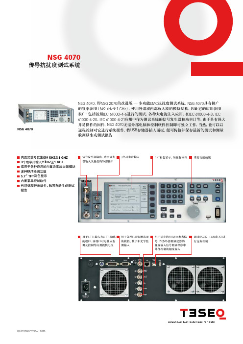
传导抗扰度测试系统NSG 4070NSG 4070,即NSG 2070的改进版 — 多功能EMC 抗扰度测试系统。
NSG 4070具有极广的频率范围(从9 kHz 至1 GHz )、使用外部或内部放大器的模块结构,因此它的应用范围很广:包括按照IEC 61000-4-6进行的测试,各种大电流注入应用,在IEC 61000-4-3、IEC61000-4-20、IEC 61000-4-21应用中作为测试系统的信号发生器和功率计等。
由于具有强大并易操作的固件,NSG 4070无需外部电脑和控制软件控制即可独立工作,当然,也可以以远程控制对它进行系统操作。
将USB 存储器插入面板,便可传输并保存最新的测试和测量数据以生成测试报告3 5.7”彩色显示、易操作固件重要功能按键通过RS232、LAN 或USB 进行远程控制内置式信号发生器9 kHz 至1 GHz 3个功率计输入9 kHz 至1 GHz适用于各种应用的内置功率放大器模块 多种EUT 检测功能 5.7” TFT 彩色显示 内置菜单控制软件 包括远程控制软件,和可自动生成测试报告NSG 40702技术指标信号发生器功率计传导抗扰度测试系统NSG 40703传导抗扰度测试系统NSG 4070正常输出功率:20 W30 W75 W频率范围:150 kHz – 230 MHz 150 kHz – 230 MHz 150 kHz – 230 MHz 输入阻抗:50 Ω50 Ω50 Ω输出阻抗:50 Ω50 Ω50 Ω输入回波损耗:最小10 dB 最小10 dB 最小10 dB 输出回波损耗:正常最小9.5 dB 、无损伤时0 dB 正常最小9.5 dB 、无损伤时0 dB 正常最小9.5 dB 、无损伤时0 dB 增益:最小46 dB 最小 46 dB 最小50 dB 增益平坦度:最大+/-3 dB 最大+/-3 dB 最大+/-3 dB 饱和输出功率:最小43 dBm 最小45 dBm 最小48.75 dBm 无损坏时最大线性输入功率:<-3.5 dBm 最大 +10 dBm < -1.5 dBm 最大+10 dBm < -3 dBm 最大+10 dBm 正常输出功率下二次谐波失真:typ. < -30 dBctyp. < -30 dBctyp. < -35 dBc正常输出功率下三次谐波失真:typ. < -20 dBc typ. < -20 dBc typ. < -18 dBc功率放大器功率计(续)4测试及测量程序固件:发生器模式固件:主发生器菜单固件:抗扰度测试设定固件:校准曲线传导抗扰度测试系统NSG 40705传导抗扰度测试系统NSG 4070Windows 软件Windows 软件: 发生器模式Windows 软件:抗扰度模式软件:发生器菜单软件:抗扰度测试设定软件:EUT 监测设定6模拟端口数字端口NSG 4070前面板与RF 射频输出口传导抗扰度测试系统NSG 40707传导抗扰度测试系统NSG 4070电源电源供电110 / 230 VAC 50 / 60 Hz 自动调节建议110 V 时用保险丝F1建议230 V 时用保险丝F1无功率放大器时的功率消耗约80 W 1 A (慢)0.5 A (慢)20 W 模式:约215 W 4 A (慢) 1.6 A (慢)30 W 模式:约240 W 4 A (慢) 1.6 A (慢)75 W 模式:约415 W6.3 A(慢) 2.5 A(慢)通用数据物理参数8IEC/EN 61000-4-6应用,CDN 校准设定IEC/EN 61000-4-6应用,采用EM 钳的校准设定IEC/EN 61000-4-6应用,采用CDN 的EUT 设定带有内置功率放大器的组合式带有内置功率放大器的组合式传导抗扰度测试系统NSG 4070NSG 4070 与KEMZ 801和CAL 8019传导抗扰度测试系统NSG 4070IEC/EN 61000-4-6应用,电流注入探头校准设定功率建议: 考虑到6dB 衰减器、0.5dB 电缆损耗、耦合装置的最大插入损耗、具有80%调制深度的AM 后可达到的测试电平IEC/EN 61000-4-6应用,采用带监视探头的EM 钳注入设定放大器模块:20 W 30 W 75 W CDN:15 V EMF 18 V EMF 30 V EMF EM 钳(KEMZ 801):8 V EMF 11 V EMF 17 V EMF 电流注入钳(CIP 9136)5 V EMF6 V EMF10 V EMF (typ.)带有内置功率放大器的组合式带有内置功率放大器的组合式10汽车电子产品BCI 测试应用,校准设置(使用外部功率放大器和定向耦合器以满足功率及频率范围要求)汽车电子产品BCI 测试应用,采用监测探头的EUT 设定NSG 4070汽车电子产品BCI 解决方案NSG 4070NSG 4070功率计Ch.1电平Ch.2前向功率Ch.3反向功率功率计Ch.1电平监测Ch.2前向功率Ch.3反向功率传导抗扰度测试系统NSG 407082-253290 C02 Dec. 201011传导抗扰度测试系统NSG 4070汽车电子产品BCI 测试应用,校准设置(使用两台功率放大器)IEC/EN 61000-4-20的应用可达1 GHz (使用外部功率放大器和定向耦合器以满足功率及频率范围要求,需要可选软件来控制场强探头)NSG 4070射频输出)NSG 4070使用端口功率计NSG 4070 datasheet 12配送信息NSG 4070系列产品配置组合式抗扰度测试系统NSG 4070、9 kHz-1 GHz RF 发生器和功率计(可选功率放大器);USB 棒上远程控制软件;备用保险丝(2);RS 232电缆(无需调制解调器);电源线GB 、CH 、USA/JP 、EU ;LAN 电缆、交叉式、3 m ;键盘;操作手册ATN 6075,6 dB 衰减器,75 Watts NSG 4070MD 4070SW 4070北京特测电子仪器有限公司北京市东直门外大街46号天恒大厦1001室(100027)T + 86 10 8460 8080 F + 86 10 8460 8078******************** 传导抗扰度测试系统NSG 4070。
BSC070N10NS3G 规格书
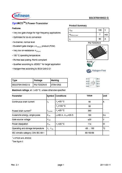
Opti MOS TM 3 Power-TransistorFeatures• Very low gate charge for high frequency applications • Optimized for dc-dc conversion • N-channel, normal level• Excellent gate charge x R DS(on) product (FOM)• Very low on-resistance R DS(on)• 150 °C operating temperature • Pb-free lead plating; RoHS compliant• Qualified according to JEDEC 1) for target application • Halogen-free according to IEC61249-2-21Maximum ratings, at T j =25 °C, unless otherwise specified ParameterSymbol Conditions Unit Continuous drain currentI DT C =25 °C 90AT C =100 °C58Pulsed drain current 2)I D,pulse T C =25 °C360Avalanche energy, single pulse E AS I D =50 A, R GS =25 W160mJ Gate source voltage V GS ±20V Power dissipationP tot T C =25 °C 114W Operating and storage temperature T j , T stg-55 ... 150°CIEC climatic category; DIN IEC 68-155/150/56Value 1)J-STD20 and JESD222)See figure 3V DS100V R DS(on),max 7m W I D90AProduct Summary TypePackage Marking BSC070N10NS3 GPG-TDSON-8070N10NSPG-TDSON-8ParameterSymbol ConditionsUnitmin.typ.max.Thermal characteristicsThermal resistance, junction - case R thJC -- 1.1K/WR thJAminimal footprint --626 cm 2 cooling area 3)--50Electrical characteristics, at T j =25 °C, unless otherwise specified Static characteristicsDrain-source breakdown voltage V (BR)DSS V GS =0 V, I D =1 mA 100--VGate threshold voltage V GS(th)V DS =V GS , I D =75 µA 2 2.7 3.5Zero gate voltage drain currentI DSSV DS =100 V, V GS =0 V, T j =25 °C-0.011µA V DS =100 V, V GS =0 V, T j =125 °C-10100Gate-source leakage current I GSS V GS =20 V, V DS =0 V -1100nA Drain-source on-state resistanceR DS(on)V GS =10 V, I D =50 A - 6.37m WV GS =6 V, I D =25 A-814Gate resistance R G - 1.5-W Transconductanceg fs|V DS |>2|I D |R DS(on)max , I D =50 A3672-S Values 3)Device on 40 mm x 40 mm x 1.5 mm epoxy PCB FR4 with 6 cm 2 (one layer, 70 µm thick) copper area for drain connection. PCB is vertical in still air.Thermal resistance, junction - ambientParameterSymbol ConditionsUnitmin.typ.max.Dynamic characteristics Input capacitance C iss -30004000pFOutput capacitanceC oss -520690Reverse transfer capacitance C rss -21-Turn-on delay time t d(on)-15-nsRise timet r -10-Turn-off delay time t d(off)-29-Fall timet f-8-Gate Charge Characteristics 4)Gate to source charge Q gs -13-nCGate to drain charge Q gd -7-Switching charge Q sw -12-Gate charge total Q g -4255Gate plateau voltage V plateau - 4.3-V Output charge Q ossV DD =50 V, V GS =0 V -5573nCReverse DiodeDiode continous forward current I S --90ADiode pulse current I S,pulse --360Diode forward voltage V SD V GS =0 V, I F =50 A, T j =25 °C-1 1.2V Reverse recovery time t rr -61-ns Reverse recovery chargeQ rr-112-nC4)See figure 16 for gate charge parameter definitionV R =50 V, I F =25 A, d i F /d t =100 A/µsT C =25 °CValues V GS =0 V, V DS =50 V, f =1 MHzV DD =50 V, V GS =10 V, I D =25 A, R G =1.6 W V DD =50 V, I D =25 A, V GS =0 to 10 V1 Power dissipation2 Drain current P tot =f(T C )I D =f(T C ); V GS ≥10 V3 Safe operating area4 Max. transient thermal impedance I D =f(V DS ); T C =25 °C; D =0Z thJC =f(t p )parameter: t pparameter: D =t p /Tsingle pulse0.010.020.050.10.20.510-510-410-310-210-110010-210-1100101Z t h J C [K /W ]t p [s]02040608010012004080120160P t o t [W ]T C [°C]010203040506070809010004080120160I D [A ]T C [°C]100 ns1 µs10 µs100 µs1 msDC10-110010110210310-1100101102103I D [A ]V DS [V]5 Typ. output characteristics6 Typ. drain-source on resistance I D =f(V DS ); T j =25 °C R DS(on)=f(I D ); T j =25 °C parameter: V GSparameter: V GS7 Typ. transfer characteristics 8 Typ. forward transconductance I D =f(V GS ); |V DS |>2|I D |R DS(on)max g fs =f(I D ); T j =25 °Cparameter: T j5 V5.5 V6 V7 V10 V02468101220406080100R D S (o n )[m W ]I D [A]25 °C150 °C020406080100246I D [A ]V GS [V]02040608010012014020406080100120140g f s [S ]I D [A]4.5 V5 V5.5 V6 V7 V10 V 020406080100120123I D [A ]V DS [V]9 Drain-source on-state resistance 10 Typ. gate threshold voltage R DS(on)=f(T j ); I D =50 A; V GS =10 VV GS(th)=f(T j ); V GS =V DS parameter: I D11 Typ. capacitances 12 Forward characteristics of reverse diode C =f(V DS ); V GS =0 V; f =1 MHzI F =f(V SD )parameter: T jtyp98 %0246810121416-60-202060100140180R D S (o n )[m W ]T j [°C]75 µA750 µA00.511.522.533.54-60-202060100140180V G S (t h )[V ]T j [°C]CissCossCrss10010110210310420406080C [p F ]V DS [V]25 °C150 °C25 °C, 98%150 °C, 98%11010010000.511.52I F [A ]V SD [V]13 Avalanche characteristics 14 Typ. gate charge I AS =f(t AV ); R GS =25 W V GS =f(Q gate ); I D =25 A pulsed parameter: T j(start)parameter: V DD15 Drain-source breakdown voltage 16 Gate charge waveformsV BR(DSS)=f(T j ); I D =1 mA20 V50 V80 V246810010********V G S [V ]Q gate [nC]9095100105110-60-202060100140180V B R (D S S )[V ]T j [°C]V GSQ gateV gs(th)Q g(th)Q gsQ gdQ swQ g25 °C100 °C125 °C1101001101001000I A S [A ]t AV [µs]Package Outline: PG-TDSON-8Dimensions in mmPublished byInfineon Technologies AG81726 Munich, Germany© 2011 Infineon Technologies AGAll Rights Reserved.Legal DisclaimerThe information given in this document shall in no event be regarded as a guarantee of conditions or characteristics. With respect to any examples or hints given herein, any typical values stated herein and/or any information regarding the application of the device,Infineon Technologies hereby disclaims any and all warranties and liabilities of any kind, including without limitation, warranties of non-infringement of intellectual property rightsof any third party.InformationFor further information on technology, delivery terms and conditions and prices, pleasecontact the nearest Infineon Technologies Office ().WarningsDue to technical requirements, components may contain dangerous substances. For information on the types in question, please contact the nearest Infineon Technologies Office.Infineon Technologies components may be used in life-support devices or systems only withthe express written approval of Infineon Technologies, if a failure of such components can reasonably be expected to cause the failure of that life-support device or system or to affectthe safety or effectiveness of that device or system. Life support devices or systems are intended to be implanted in the human body or to support and/or maintain and sustainand/or protect human life. If they fail, it is reasonable to assume that the health of the useror other persons may be endangered.。
CXG1090EN中文资料
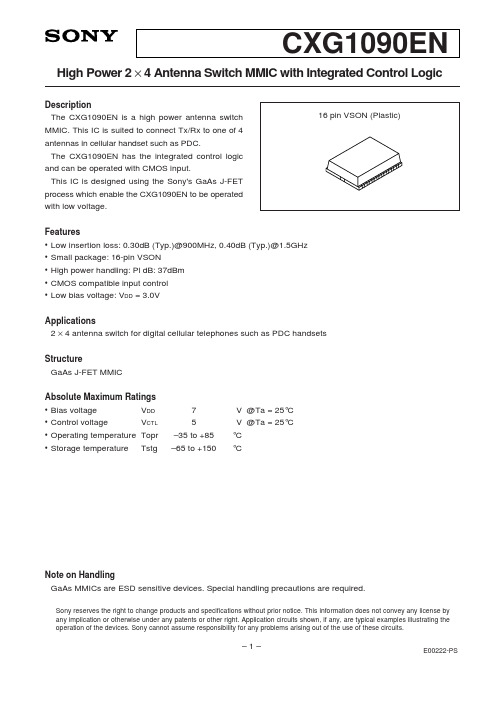
CXG1090ENHigh Power 2 ×4 Antenna Switch MMIC with Integrated Control LogicDescriptionThe CXG1090EN is a high power antenna switch MMIC. This IC is suited to connect Tx/Rx to one of 4antennas in cellular handset such as PDC.The CXG1090EN has the integrated control logic and can be operated with CMOS input.This IC is designed using the Sony's GaAs J-FET process which enable the CXG1090EN to be operated with low voltage.Features•Low insertion loss: 0.30dB (Typ.)@900MHz, 0.40dB (Typ.)@1.5GHz •Small package: 16-pin VSON•High power handling: Pl dB: 37dBm •CMOS compatible input control •Low bias voltage: V DD = 3.0VApplications2 ×4 antenna switch for digital cellular telephones such as PDC handsets StructureGaAs J-FET MMICAbsolute Maximum Ratings •Bias voltage V DD 7V @Ta = 25°C •Control voltage V CTL 5V @Ta = 25°C •Operating temperature Topr –35 to +85°C •Storage temperature Tstg–65 to +150°CNote on HandlingGaAs MMICs are ESD sensitive devices. Special handling precautions are required.– 1–E00222-PSSony reserves the right to change products and specifications without prior notice. This information does not convey any license by any implication or otherwise under any patents or other right. Application circuits shown, if any, are typical examples illustrating the operation of the devices. Sony cannot assume responsibility for any problems arising out of the use of these circuits.16 pin VSON (Plastic)– 2–Block Diagram RF5(Rx)RF4(Ant/Ext.1)RF6(Diversity 1)RF2(Ant/Ext. 2)RF3(Tx)RF1(Diversity 2)RF-GND6RF-GND1Pin ConfigurationRF4GND RF5GND RF6RF-GND6V DD CTLA RF3GND RF2GND RF1RF-GND1CTLC CTLBRecommended CircuitRF3GND GND RF-GND1RF2RF4V RF5GND GNDRF-GND6RF6RF1∗DC blocking capacitors (CRF) are needed.∗Recommended to use bypass capacitors (Cbypass).∗Recommended to use control resistors (RCTL), when it is necessary to improve the electrostatic discharge strength (ESD).Truth TableControlON F1F2F3F4F5F6F7F8 CTLAH H L L L LLLLLHHLHLHLHRF3 →RF2RF3 →RF4RF5 →RF2RF5 →RF4RF5 →RF6RF5 →RF1OFFONONOFFOFFOFFONOFFOFFONOFFOFFOFFONONOFFOFFOFFONOFFOFFONOFFOFFOFFOFFOFFOFFONOFFOFFOFFOFFOFFOFFONONONONONOFFONONONONONONOFF CTLB CTLCDC Bias Condition(Ta = 25°C) ItemV CTL(H) A to C V CTL(L) A to C V DD 2.42.83.60.83.2VVVMin.Typ.Max.Unit– 3–– 4–ItemFrequencyConditionPin = 29.5dBm, V DD = 2.8 to 3.0V Pin = 29.5dBm, V DD = 2.8 to 3.0VPin = 7dBm, V DD = 2.8 to 3.0V Pin = 7dBm, V DD = 2.8 to 3.0V Pin = 7dBm, V DD = 2.8 to 3.0V Pin = 7dBm, V DD = 2.8 to 3.0V Pin = 29.5dBm, V DD = 2.8 to 3.0V Pin = 29.5dBm, V DD = 2.8 to 3.0VPin = 7dBm, V DD = 2.8 to 3.0V Pin = 7dBm, V DD = 2.8 to 3.0V Pin = 7dBm, V DD = 2.8 to 3.0V Pin = 7dBm, V DD = 2.8 to 3.0VPin = 29.5dBm, V DD = 3.0V ∗1Pin = 29.5dBm, V DD = 2.8V ∗1Pin = 29.5dBm, V DD = 3.0V ∗1Pin = 29.5dBm, V DD = 2.8V ∗1Pin = 29.5dBm, V DD = 3.0V ∗1Pin = 29.5dBm, V DD = 2.8V ∗1Pin = 29.5dBm, V DD = 3.0V ∗1Pin = 29.5dBm, V DD = 2.8V ∗1V DD = 3.0V V DD = 2.8V1717171731240.320.300.550.550.50.5192121193829–67–67–75–75–67–67–67–67850.450.41.00.550.550.850.850.80.81.4–57–55–65–62–60–57–60–5715010.95.0dB dB dB dB dB dB dB dB dB dB dB dBdBc dBc dBc dBc dBc dBc dBc dBc µA mA mA µsRF3-RF2RF3-RF4RF5-RF2RF5-RF4RF5-RF1RF5-RF6RF3-RF2RF3-RF4RF5-RF2RF5-RF4RF5-RF1RF5-RF6Each ONPortRF3-RF2RF3-RF4RF3-RF2RF3-RF4RF3-RF2RF3-RF4RF3-RF2RF3-RF4Insertion lossIsolationVSWR ACP (±50kHz)ACP (±100kHz)2nd harmonics3nd harmonics Control current Bias current Switching speed889 to 960MHz 889 to 960MHz 810 to 885MHz 810 to 885MHz 810 to 885MHz 810 to 885MHz 889 to 960MHz 889 to 960MHz 810 to 885MHz 810 to 885MHz 810 to 885MHz 810 to 885MHz 810 to 960MHz889 to 960MHz889 to 960MHz889 to 960MHz889 to 960MHzMin.Typ.Max.Unit ∗1Input signal: ACP (±50kHz) < –65dBc, APC (±100kHz) < –75dBc,2nd harmonics < –65dBc, 3rd harmonics < –65dBc– 5–ItemFrequencyConditionPin = 29.5dBm, V DD = 2.8 to 3.0V Pin = 29.5dBm, V DD = 2.8 to 3.0VPin = 7dBm, V DD = 2.8 to 3.0V Pin = 7dBm, V DD = 2.8 to 3.0V Pin = 7dBm, V DD = 2.8 to 3.0V Pin = 7dBm, V DD = 2.8 to 3.0V Pin = 29.5dBm, V DD = 2.8 to 3.0V Pin = 29.5dBm, V DD = 2.8 to 3.0VPin = 7dBm, V DD = 2.8 to 3.0V Pin = 7dBm, V DD = 2.8 to 3.0V Pin = 7dBm, V DD = 2.8 to 3.0V Pin = 7dBm, V DD = 2.8 to 3.0VPin = 29.5dBm, V DD = 3.0V ∗1Pin = 29.5dBm, V DD = 2.8V ∗1Pin = 29.5dBm, V DD = 3.0V ∗1Pin = 29.5dBm, V DD = 2.8V ∗1Pin = 29.5dBm, V DD = 3.0V ∗1Pin = 29.5dBm, V DD = 2.8V ∗1Pin = 29.5dBm, V DD = 3.0V ∗1Pin = 29.5dBm, V DD = 2.8V ∗1V DD = 3.0V V DD = 2.8V1215151335200.400.400.650.650.600.60151818164025–67–67–75–75–67–67–67–67850.450.41.00.700.700.950.950.900.901.4–55–53–65–62–60–57–57–5515010.95.0dB dB dB dB dB dB dB dB dB dB dB dBdBc dBc dBc dBc dBc dBc dBc dBc µA mA mA µsRF3-RF2RF3-RF4RF5-RF2RF5-RF4RF5-RF1RF5-RF6RF3-RF2RF3-RF4RF5-RF2RF5-RF4RF5-RF1RF5-RF6Each ONPortRF3-RF2RF3-RF4RF3-RF2RF3-RF4RF3-RF2RF3-RF4RF3-RF2RF3-RF4Insertion lossIsolationVSWR ACP (±50kHz)ACP (±100kHz)2nd harmonics3nd harmonics Control current Bias current Switching speed1429 to 1453MHz 1429 to 1453MHz 1477 to 1501MHz 1477 to 1501MHz 1477 to 1501MHz 1477 to 1501MHz 1429 to 1453MHz 1429 to 1453MHz 1477 to 1501MHz 1477 to 1501MHz 1477 to 1501MHz 1477 to 1501MHz 1429 to 1501MHz1429 to 1453MHz1429 to 1453MHz1429 to 1453MHz1429 to 1453MHzMin.Typ.Max.Unit ∗1Input signal: ACP (±50kHz) < –65dBc, APC (±100kHz) < –75dBc,2nd harmonics < –65dBc, 3rd harmonics < –65dBc– 6–Package Outline Unit: mmSONY CODE EIAJ CODE JEDEC CODEPACKAGE MATERIALLEAD TREATMENT LEAD MATERIAL PACKAGE MASSEPOXY RESIN SOLDER PLATING COPPER ALLOY PACKAGE STRUCTURETERMINAL SECTIONranges of 0.1mm and 0.25mm from the end of a terminal.NOTE:1) The dimensions of the terminal section apply to the 16PIN VSON(PLASTIC)VSON-16P-010.02 g。
BSC数据配-数据配置基础知识(PDF 67页)

配置 BSC 数据的设定应该遵循从全局到局部的原则。BSC 的数据配置可分为 AM/CM 数据、BM 数据两大块。在每一块中,又遵循模块→机架→机框→单板→系 统资源的配置顺序,如图 B-1所示。
GSM-R 基站控制器 数据配置手册 初始配置分册
目录
目录
附录 B 数据配置基础知识 ........................................................................................................ B-1 B.1 BSC 数据 ........................................................................................................................... B-1 B.1.1 配置原则与流程 ...................................................................................................... B-1 B.1.2 编号原则................................................................................................................. B-2 B.1.3 AM/CM 数据配置..................................................................................................... B-4 B.1.4 BM 数据配置 ........................................................................................................... B-6 B.2 时钟系统 ......................................................................................................................... B-10 B.3 A 接口中继与信令 ............................................................................................................ B-12 B.4 基站组网 ......................................................................................................................... B-13 B.4.1 编号原则............................................................................................................... B-13 B.4.2 BIE 介绍 ................................................................................................................ B-14 B.4.3 星型组网............................................................................................................... B-17 B.4.4 链型组网............................................................................................................... B-23 B.4.5 树型组网............................................................................................................... B-45 B.4.6 半速率组网 ........................................................................................................... B-46 B.4.7 环型组网............................................................................................................... B-49
BSC操作维护手册终稿
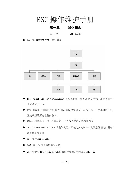
BSC操作维护手册第一章MO概念第一节MO结构●MO:(MANAGEDOBJECT)管理对象;●BSC:(BASE STATION CONTROLLER)基站控制器,属GSM网络单元,用于控制一个或若干个BTS;●BTS:(BASE TRANSCEIVER STATION)GSM网络单元,是指工作于一个小区的一组无线载频的所有设备的总和;●CELL:蜂窝小区,指一个基站的一个天线系统的无线覆盖范围;●TG:(TRANSCEIVER GROUP)收发信机组,即被定义为和一个天线系统相连的所有收发信机的总和;●CF:支持BTS的O&M;●CON:用于对信令的集中与分解;●IS:用于对BSC和TRU的PCM时隙进行交换、标准是16KBIT/S;●TF:(TIMING FUNCTION)同TM相关联的逻辑单元,提供TRU的时钟信号,用于产生TDMA帧和无线频率参考信号;●DP:用于对传输质量和故障进行监测;●TRX:(TRANSCEIVER)收发信机,GSM网络实体,用于无线发射/接收以及信号处理,它与8个BPC上的话务相关联,即与属于一个TDMA帧的所有BPC相关联;●TRXC:(TRANSCEIVERCONTRALLER)RBS200的硬件单元,它通过所属的RRX和SPP控制8个BPC,TRXC作为TGC时,它主控该TG的公共资源,即主控TRX和TM;●RTX:(RADIOTRANSMITTER)无线发射机,RBS200的硬件单元,用于射频发射的调制;●RRX:(RADIORECEIVER)无线接收机,RBS200的硬件单元,用于接收和处理射频信号;●TX:(TRANSMITTER)与RTX相关联的逻辑单元;●RX:(RECEIVER)同RRX相关联的逻辑单元;●TS:TIMESLOT,即载波时隙,相应于TDMA帧子单元,TDMA帧中的8个时隙被编为0-7;第二节MO状态1MO的各种通用状态UNDEF:MO没有定义。
BSC054N04NS G中文资料
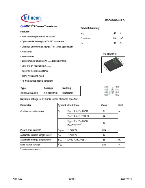
ValueUnit 81ABSC054N04NS GMaximum ratings, at T j =25 °C, unless otherwise specified Parameter Symbol Conditions Unit Power dissipationP totT C =25 °C 57WT A =25 °C, R thJA =50 K/W 2)2.5Operating and storage temperature T j , T stg-55 ... 150°C IEC climatic category; DIN IEC 68-155/150/56Parameter Symbol ConditionsUnitmin.typ.max.Thermal characteristicsThermal resistance, junction - caseR thJCbottom -- 2.2K/Wtop--20Device on PCBR thJA6 cm 2 cooling area 2)--50Electrical characteristics, at T j =25 °C, unless otherwise specified Static characteristicsDrain-source breakdown voltage V (BR)DSS V GS =0 V, I D =1 mA 40--VGate threshold voltage V GS(th)V DS =V GS , I D =27 µA 2-4Zero gate voltage drain currentI DSSV DS =40 V, V GS =0 V, T j =25 °C-0.11µAV DS =40 V, V GS =0 V, T j =125 °C-10100Gate-source leakage current I GSS V GS =20 V, V DS =0 V -10100nA Drain-source on-state resistance R DS(on)V GS =10 V, I D =50 A- 4.5 5.4m ΩGate resistance R G -1.5-ΩTransconductanceg fs|V DS |>2|I D |R DS(on)max , I D =50 A3467-S4)See figure 13 for more detailed information3) See figure 3 for more detailed information Value Values 2)Device on 40 mm x 40 mm x 1.5 mm epoxy PCB FR4 with 6 cm 2(one layer, 70 µm thick) copper area for drain connection. PCB is vertical in still air.BSC054N04NS GParameter Symbol Conditions Unitmin.typ.max. Dynamic characteristicsInput capacitance C iss-21002800pF Output capacitance C oss-620820 Reverse transfer capacitance C rss-22-Turn-on delay time t d(on)-11-ns Rise time t r- 2.6-Turn-off delay time t d(off)-16-Fall time t f- 3.6-Gate Charge Characteristics5)Gate to source charge Q gs-11-nC Gate charge at threshold Q g(th)- 6.3-Gate to drain charge Q gd- 3.3-Switching charge Q sw-8.2-Gate charge total Q g-2634Gate plateau voltage V plateau- 5.3-VGate charge total, sync. FET Q g(sync)V DS=0.1 V,V GS=0 to 10 V-24-nCOutput charge Q oss V DD=20 V, V GS=0 V-23-Reverse DiodeDiode continuous forward current I S--47A Diode pulse current I S,pulse--324Diode forward voltage V SD V GS=0 V, I F=50 A,T j=25 °C-0.91 1.2VReverse recovery charge Q rr V R=20 V, I F=I S,d i F/d t=400 A/µs-27-nC5) See figure 16 for gate charge parameter definition T C=25 °CValuesV GS=0 V, V DS=20 V,f=1 MHzV DD=20 V, V GS=10 V,I D=30 A, R G=1.6 ΩV DD=20 V, I D=30 A,V GS=0 to 10 VBSC054N04NS G Package Outline PG-TDSON-8PG-TDSON-8: OutlineFootprintBSC054N04NS G Package OutlinePG-TDSON-8: TapeBSC054N04NS GPublished byInfineon Technologies AG81726 Munich, Germany© 2008 Infineon Technologies AGAll Rights Reserved.Legal DisclaimerThe information given in this document shall in no event be regarded as a guarantee ofconditions or characteristics. With respect to any examples or hints given herein, any typicalvalues stated herein and/or any information regarding the application of the device,Infineon Technologies hereby disclaims any and all warranties and liabilities of any kind,including without limitation, warranties of non-infringement of intellectual property rightsof any third party.InformationFor further information on technology, delivery terms and conditions and prices, pleasecontact the nearest Infineon Technologies Office().WarningsDue to technical requirements, components may contain dangerous substances. For informationon the types in question, please contact the nearest Infineon Technologies Office.Infineon Technologies components may be used in life-support devices or systems only withthe express written approval of Infineon Technologies, if a failure of such components canreasonably be expected to cause the failure of that life-support device or system or to affectthe safety or effectiveness of that device or system. Life support devices or systems areintended to be implanted in the human body or to support and/or maintain and sustainand/or protect human life. If they fail, it is reasonable to assume that the health of the useror other persons may be endangered.。
BSC082N10LS G中文资料

Opti MOS®ValueUnitBSC082N10LS GParameterSymbol ConditionsUnitmin.typ.max.Thermal characteristicsThermal resistance, junction - caseR thJCbottom --0.8K/Wtop--18R thJAminimal footprint --626 cm 2 cooling area 2)--45Electrical characteristics, at T j =25 °C, unless otherwise specified Static characteristicsDrain-source breakdown voltage V (BR)DSS V GS =0 V, I D =1 mA 100--VGate threshold voltage V GS(th)V DS =V GS , I D =110 µA 1.2 1.85 2.4Zero gate voltage drain currentI DSSV DS =100 V, V GS =0 V, T j =25 °C-0.011µA V DS =100 V, V GS =0 V, T j =125 °C-10100Gate-source leakage current I GSS V GS =20 V, V DS =0 V -1100nA Drain-source on-state resistanceR DS(on)V GS =4.5 V, I D =50 A -8.211m ΩV GS =10 V, I D =100 A- 6.88.2Gate resistance R G -1-ΩTransconductanceg fs|V DS |>2|I D |R DS(on)max , I D =50 A60119-S Values 2)Device on 40 mm x 40 mm x 1.5 mm epoxy PCB FR4 with 6 cm 2(one layer, 70 µm thick) copper area for drain connection. PCB is vertical in still air.Thermal resistance, junction - ambient3)see figure 3BSC082N10LS GParameterSymbol ConditionsUnitmin.typ.max.Dynamic characteristics Input capacitance C iss -56007400pFOutput capacitanceC oss -710940Reverse transfer capacitance C rss -3857Turn-on delay time t d(on)-1928nsRise timet r -2436Turn-off delay time t d(off)-5380Fall timet f-1217Gate Charge Characteristics 4)Gate to source charge Q gs -1823nCGate to drain charge Q gd -1319Switching charge Q sw -2130Gate charge total Q g -78104Gate plateau voltage V plateau - 3.1-V Output charge Q ossV DD =50 V, V GS =0 V -7397nCReverse DiodeDiode continous forward current I S --100ADiode pulse current I S,pulse --400Diode forward voltage V SD V GS =0 V, I F =50 A, T j =25 °C-0.9 1.2V Reverse recovery time t rr -107-ns Reverse recovery chargeQ rr-226-nC4)See figure 16 for gate charge parameter definitionV R =50 V, I F =25 A, d i F /d t =100 A/µsT C =25 °CValues V GS =0 V, V DS =50 V, f =1 MHzV DD =50 V, V GS =10 V, I D =25 A, R G =2.7 ΩV DD =50 V, I D =25 A, V GS =0 to 10 V1 Power dissipation5 Typ. output characteristics9 Drain-source on-state resistance13 Avalanche characteristicsBSC082N10LS G Package Outline: PG-TDSON-8BSC082N10LS GDimensions in mmBSC082N10LS GPublished byInfineon Technologies AG81726 Munich, Germany© 2008 Infineon Technologies AGAll Rights Reserved.Legal DisclaimerThe information given in this document shall in no event be regarded as a guarantee ofconditions or characteristics. With respect to any examples or hints given herein, any typicalvalues stated herein and/or any information regarding the application of the device,Infineon Technologies hereby disclaims any and all warranties and liabilities of any kind,including without limitation, warranties of non-infringement of intellectual property rightsof any third party.InformationFor further information on technology, delivery terms and conditions and prices, pleasecontact the nearest Infineon Technologies Office ().WarningsDue to technical requirements, components may contain dangerous substances. For informationon the types in question, please contact the nearest Infineon Technologies Office.Infineon Technologies components may be used in life-support devices or systems only withthe express written approval of Infineon Technologies, if a failure of such components canreasonably be expected to cause the failure of that life-support device or system or to affectthe safety or effectiveness of that device or system. Life support devices or systems areintended to be implanted in the human body or to support and/or maintain and sustainand/or protect human life. If they fail, it is reasonable to assume that the health of the useror other persons may be endangered.。
GSM0710中文版
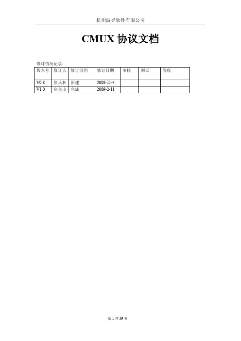
杭州波导软件有限公司
3.4. 过程和状态..................................................................................................................... 20 3.4.1. 建立 DLC 链路 ........................................................................................ 20 3.4.2. 释放 DLC 链路 ........................................................................................ 20 3.4.3. 信息传输 .................................................................................................. 21 3.4.4. 帧变量...................................................................................................... 21 3.4.5. 超时的考虑 .............................................................................................. 22 3.4.6. 多路控制通道 .......................................................................................... 22 3.4.6.1. 控制消息格式........................................................................................... 22 3.4.6.2. 控制消息类型参数 ................................................................................... 23 3.4.7. 电源控制与唤醒机制 .............................................................................. 32 3.4.8. 流控.......................................................................................................... 32 3.5. 集成层 Convergence Layer ............................................................................................ 34 3.5.1. 类型 1-未结构化的字节流...................................................................... 34 3.5.2. 类型 2-带参数的未结构化的字节流...................................................... 34 3.5.3. 类型 3-不可中断的帧数据...................................................................... 36 3.5.4. 类型 4-可中断的帧数据.......................................................................... 36 3.6. DLCI 值 ........................................................................................................................... 37 3.7. 系统参数......................................................................................................................... 37 3.7.1. 确认时间 T1 ............................................................................................ 37 3.7.2. 帧的最大长度 N1 .................................................................................... 38 3.7.3. 最大重发次数 N2 .................................................................................... 38 3.7.4. 窗口大小 k ............................................................................................... 38 3.7.5. 控制通道的响应时间 T2 ........................................................................ 38 3.7.6. 唤醒流程的响应时间 T3 ........................................................................ 38 3.8. 启动和关闭 MUX .......................................................................................................... 38 4. Error Recovery Mode ................................................................................................................. 39
BSC027N04LS G中文资料

ValueUnit 100ABSC027N04LS GMaximum ratings, at T j=25 °C, unless otherwise specifiedParameter Symbol Conditions Unit Power dissipation P tot T C=25 °C83WT A=25 °C,R thJA=50 K/W2)2.5Operating and storage temperature T j, T stg-55 ... 150°C IEC climatic category; DIN IEC 68-155/150/56Parameter Symbol Conditions Unitmin.typ.max. Thermal characteristicsThermal resistance, junction - case R thJC bottom-- 1.5K/Wtop18Device on PCB R thJA 6 cm2 cooling area2)--50 Electrical characteristics, at T j=25 °C, unless otherwise specifiedStatic characteristicsDrain-source breakdown voltage V(BR)DSS V GS=0 V, I D=1 mA40--V Gate threshold voltage V GS(th)V DS=V GS, I D=49 µA 1.2-2Zero gate voltage drain current I DSS V DS=40 V, V GS=0 V,T j=25 °C-0.11µAV DS=40 V, V GS=0 V,T j=125 °C-10100Gate-source leakage current I GSS V GS=20 V, V DS=0 V-10100nA Drain-source on-state resistance R DS(on)V GS=4.5 V, I D=50 A- 3.3 4.1mΩV GS=10 V, I D=50 A- 2.3 2.7Gate resistance R G- 1.6-ΩTransconductance g fs |V DS|>2|I D|R DS(on)max,I D=50 A70140-S3) See figure 3 for more detailed informationValue Values2) Device on 40 mm x 40 mm x 1.5 mm epoxy PCB FR4 with 6 cm2 (one layer, 70 µm thick) copper area for drain connection. PCB is vertical in still air.BSC027N04LS GParameter Symbol Conditions Unitmin.typ.max. Dynamic characteristicsInput capacitance C iss-51006800pF Output capacitance C oss-11001500 Reverse transfer capacitance C rss-59-Turn-on delay time t d(on)-9.8-ns Rise time t r- 5.6-Turn-off delay time t d(off)-39-Fall time t f- 6.2-Gate Charge Characteristics5)Gate to source charge Q gs-15-nC Gate charge at threshold Q g(th)-8.1-Gate to drain charge Q gd- 6.5-Switching charge Q sw-14-Gate charge total Q g-6485Gate plateau voltage V plateau- 3.0-VGate charge total Q g V DD=20 V, I D=30 A,V GS=0 to 4.5 V-3141nCGate charge total, sync. FET Q g(sync)V DS=0.1 V,V GS=0 to 10 V-60-Output charge Q oss V DD=20 V, V GS=0 V-40-Reverse DiodeDiode continuous forward current I S--69A Diode pulse current I S,pulse--400Diode forward voltage V SD V GS=0 V, I F=50 A,T j=25 °C-0.83 1.2VReverse recovery charge Q rr V R=20 V, I F=I S,d i F/d t=400 A/µs-45-nC T C=25 °CValuesV GS=0 V, V DS=20 V,f=1 MHzV DD=20 V, V GS=10 V,I D=30 A, R G=1.6 ΩV DD=20 V, I D=30 A,V GS=0 to 10 VBSC027N04LS G Package Outline PG-TDSON-8PG-TDSON-8: OutlineFootprintBSC027N04LS G Package OutlinePG-TDSON-8: TapeBSC027N04LS GPublished byInfineon Technologies AG81726 Munich, Germany© 2008 Infineon Technologies AGAll Rights Reserved.Legal DisclaimerThe information given in this document shall in no event be regarded as a guarantee ofconditions or characteristics. With respect to any examples or hints given herein, any typicalvalues stated herein and/or any information regarding the application of the device,Infineon Technologies hereby disclaims any and all warranties and liabilities of any kind,including without limitation, warranties of non-infringement of intellectual property rightsof any third party.InformationFor further information on technology, delivery terms and conditions and prices, pleasecontact the nearest Infineon Technologies().WarningsDue to technical requirements, components may contain dangerous substances. For informationon the types in question, please contact the nearest Infineon Technologies Office.Infineon Technologies components may be used in life-support devices or systems only withthe express written approval of Infineon Technologies, if a failure of such components canreasonably be expected to cause the failure of that life-support device or system or to affectthe safety or effectiveness of that device or system. Life support devices or systems areintended to be implanted in the human body or to support and/or maintain and sustainand/or protect human life. If they fail, it is reasonable to assume that the health of the useror other persons may be endangered.。
NOKIABSC简介

PPT文档演模板
2024/2/8
NOKIABSC简介
BSC3000设备说明
BSC3000设备容量 可带载频3000块 最大处理18000erl TC单元最大容量96 PCU单元最大容量60个新型PCU 可提供16个STM-1/OC-3 接口 或800个E1/T1 接口 最大支持30720个16kbit/s GPRS信 道
Exchange Terminal (ET单元)
根据传输数据不同分为Abis,A(Ater),GB接口
PPT文档演模板
NOKIABSC简介
BSC设备组成(TC部分)
TCSM2机柜
✓一个TC机柜最多容纳8个TC单 元,即在BSC上看到的TCSM单 元。
✓每个TC单元由ET部分和TCIC 组成。
✓TCSM单元有5对传输线,其中 第一对是到BSC端(Ater口), 剩余4对连接到MSC或者MGW( A口)
查询单元板件类型 查询GB口NSEI状态
查询GB口NSVCI配置 查询ET用于何种接口(A,Abis或者GB)
PPT文档演模板
NOKIABSC简介
常用的BSC操作命令
常用的BSC操作命令:ZEEI、ZEEL、ZERO、ZEQO、ZEAO、 ZAHO、ZERS、ZEQS、ZERM、ZEQM、ZEHO、ZDSB等
MCMU GSWB
BSC
BCSU
LANU
GTIC TC2C
TC
SGSN
MGW
交换
PPT文档演模板
NOKIABSC简介
BSC容量以及负荷要求
BSC容量主要有三方面:
A口 信令负荷 话务负荷
可以用ZOLT命令查询,查询值小于1为正常,由网优规划 由A口话务电路数和BSC用户接入数决定
监控室基础知识培训
(第一期)
1
AXE10:是一种全数字集中的控制的程控交换机,可在移动网, 公网上使用。AXE10由APZ和APT两大部分组成。
AXE10
APZ
APT
CPS
RPS
IOS
MAS
TCS
TSS
GSS
CPS: MAS: RPS:
中央处理机子系统 维护子系统 区域处理机子系统
寄存器功能块
17
GSM 服务区
PLMN 服务区 MSC\VLR 服务区 位置区 小区
图3 CME20的网络结构
18
每个MSC/VLR服务区又被分成若干个位置区,位置 区是MSC/VLR服务区的一个部分,在一个位置区内,移 动台可以自由地移动,不需做位置更新。一个位置区是
广播寻呼消息以便找到某移动用户的寻呼区域。一个位
16
7、 小区全球识别码(CGI)
CGI用于识别一个位置区内的小区。它是在位置区识别码 (LAI)后加一个小区识别码(CI)构成的:
CGI = MCC + MNC + LAC + CI
其中CI最长也为16bits,即一个位置区内理论上最多也可 定义65536个小区。 可在BSC用指令:RLDEP:CELL= ;查看某小区的CGI
置区只能属于某一个MSC/VLR。利用位置区识别码 (LAI),系统能够区别不同的位置区。
一个位置区又划分为若干个小区。每个小区具有专用 的识别码(CGI),它表示网络中一个基本的无线覆盖 区域。注意:ERCSSON划分LA几乎与MSC服务区一样大, LA大,寻呼效率低:LA 小,要频繁地做位置更新, 网络信令流量加大,手机电池也不耐用。建议在信令 不超载的情况下,尽可能划大位置区。
S-80730SN-DT-X中文资料
VSS 3 * Parasitic diode Figure 2
2
Seiko Instruments Inc.
元器件交易网
2.0 V±2.4% 2.1 V±2.4% 2.2 V±2.4% 2.3 V±2.4% 2.4 V±2.4% 2.5 V±2.4% 2.6 V±2.4% 2.7 V±2.4% 2.8 V±2.4% 2.9 V±2.4% 3.0 V±2.4% 3.1 V±2.4% 3.2 V±2.4% 3.3 V±2.4% 3.4 V±2.4% 3.5 V±2.4% 3.6V±2.4% 3.7V±2.4% 3.8 V±2.4% 3.9 V±2.4% 4.0 V±2.4% 4.1 V±2.4% 4.2 V±2.4% 4.3 V±2.4% 4.4 V±2.4% 4.295 to 4.605 4.5 V±2.4% 4.6 V±2.4% 4.7 V±2.4% 4.8 V±2.4% 4.9 V±2.4% 5.0 V±2.4% 5.1 V±2.4% 5.2 V±2.4% 5.3 V±2.4% 5.5 V±2.4% 6.1 V±2.4% 6.3 V±2.4% 7.7V±2.4%
元器件交易网
Contents
Features........................................................... 1 Applications ..................................................... 1 Pin Assignment................................................ 1 Block Diagram ................................................. 2 Selection Guide ............................................... 3 Output Configurations...................................... 4 Advantage over the S-805 Series.................... 5 Absolute Maximum Ratings............................. 6 Electrical Characteristics ................................. 7 Test Circuits................................................... 23 Technical Terms ............................................ 24 Operation ....................................................... 26 Dimensions.................................................... 28 Taping............................................................ 29 Magazine Dimensions ................................... 31 Markings ........................................................ 32 Characteristics............................................... 33 Measuring Circuits ......................................... 36 Application Circuit Examples ......................... 37 Notes ............................................................. 39 Frequently Asked Questions......................... 40
nr电感规格及型号参数

nr电感规格及型号参数
【原创版】
目录
1.NR 磁胶电感的常用规格参数
2.工字电感规格与参数常用型号
3.NVH820S75L4SPC专业电源管理IC/ON规格参数
正文
一、NR 磁胶电感的常用规格参数
R 磁胶电感是一种常见的电子元器件,其常用规格尺寸包括
xlcs201610、xlcs252010、xlcs252012 和 xlcs3type(型号) 等。
这些规格分别对应不同的尺寸和参数,如 2.00.3、1.60.3、1.05、max、0.60.2、
0.770.2、0.6、0.8、1.8、1 等。
二、工字电感规格与参数常用型号
工字电感是一种广泛应用于电路匹配和信号质量控制的电子元器件。
其线圈的线径一般较粗,表现为直流电阻较小,通过的电流较大。
工字电感常用规格型号有 pk0304、pk0406、pk0507、pk0707、pk0608、pk0810、pk09 等。
三、NVH820S75L4SPC 专业电源管理 IC/ON 规格参数
VH820S75L4SPC是一款专业的电源管理IC/ON,其详细规格参数包括:2023-06-13报道,BCM5719A1KFBG Broadcom 630 2 年内、
DS90UB964TRGCRQ1 TI 2K 2 年内、M74VHC1GT50DFT1G ON 12K 2 年内等。
第1页共1页。
- 1、下载文档前请自行甄别文档内容的完整性,平台不提供额外的编辑、内容补充、找答案等附加服务。
- 2、"仅部分预览"的文档,不可在线预览部分如存在完整性等问题,可反馈申请退款(可完整预览的文档不适用该条件!)。
- 3、如文档侵犯您的权益,请联系客服反馈,我们会尽快为您处理(人工客服工作时间:9:00-18:30)。
Opti MOS®
Value
Unit
BSC079N10NS G
Parameter
Symbol Conditions
Unit
min.
typ.
max.
Thermal characteristics
Thermal resistance, junction - case
R thJC
bottom --0.8K/W
top
--18R thJA
minimal footprint --626 cm 2 cooling area 2)
--45
Electrical characteristics, at T j =25 °C, unless otherwise specified Static characteristics
Drain-source breakdown voltage V (BR)DSS V GS =0 V, I D =1 mA 100--V
Gate threshold voltage V GS(th)V DS =V GS , I D =110 µA 234Zero gate voltage drain current
I DSS
V DS =100 V, V GS =0 V, T j =25 °C
-0.01
1
µA V DS =100 V, V GS =0 V, T j =125 °C
-10100Gate-source leakage current I GSS V GS =20 V, V DS =0 V -1100nA Drain-source on-state resistance R DS(on)V GS =10 V, I D =50 A
- 6.67.9m ΩGate resistance R G -1-ΩTransconductance
g fs
|V DS |>2|I D |R DS(on)max , I D =50 A
40
80
-S
Values 2)
Device on 40 mm x 40 mm x 1.5 mm epoxy PCB FR4 with 6 cm 2
(one layer, 70 µm thick) copper area for drain connection. PCB is vertical in still air.Thermal resistance, junction - ambient
3)
see figure 3
BSC079N10NS G
Parameter
Symbol Conditions
Unit
min.
typ.
max.
Dynamic characteristics Input capacitance C iss -44005900pF
Output capacitance
C oss -660880Reverse transfer capacitance C rss -3857Turn-on delay time t d(on)-2436ns
Rise time
t r -4060Turn-off delay time t d(off)-3857Fall time
t f
-
11
17
Gate Charge Characteristics 4)Gate to source charge Q gs -2229nC
Gate to drain charge Q gd -1523Switching charge Q sw -3043Gate charge total Q g -6687Gate plateau voltage V plateau - 5.1-V Output charge Q oss
V DD =50 V, V GS =0 V -
70
92
nC
Reverse Diode
Diode continous forward current I S --100A
Diode pulse current I S,pulse --400Diode forward voltage V SD V GS =0 V, I F =50 A, T j =25 °C
-0.9 1.2
V Reverse recovery time t rr -107ns Reverse recovery charge
Q rr
-
231
nC
4)
See figure 16 for gate charge parameter definition
V R =15 V, I F =50 A, d i F /d t =400 A/µs
T C =25 °C
Values V GS =0 V, V DS =50 V, f =1 MHz
V DD =50 V, V GS =10 V, I D =50 A, R G =1.6 ΩV DD =50 V, I D =50 A, V GS =0 to 10 V
1 Power dissipation
5 Typ. output characteristics
9 Drain-source on-state resistance
13 Avalanche characteristics
BSC079N10NS G Package Outline: PG-TDSON-8
BSC079N10NS G
Dimensions in mm
BSC079N10NS G
Published by
Infineon Technologies AG
81726 Munich, Germany
© 2008 Infineon Technologies AG
All Rights Reserved.
Legal Disclaimer
The information given in this document shall in no event be regarded as a guarantee of
conditions or characteristics. With respect to any examples or hints given herein, any typical
values stated herein and/or any information regarding the application of the device,
Infineon Technologies hereby disclaims any and all warranties and liabilities of any kind,
including without limitation, warranties of non-infringement of intellectual property rights
of any third party.
Information
For further information on technology, delivery terms and conditions and prices, please
contact the nearest Infineon Technologies Office ().
Warnings
Due to technical requirements, components may contain dangerous substances. For information
on the types in question, please contact the nearest Infineon Technologies Office.
Infineon Technologies components may be used in life-support devices or systems only with
the express written approval of Infineon Technologies, if a failure of such components can
reasonably be expected to cause the failure of that life-support device or system or to affect
the safety or effectiveness of that device or system. Life support devices or systems are
intended to be implanted in the human body or to support and/or maintain and sustain
and/or protect human life. If they fail, it is reasonable to assume that the health of the user
or other persons may be endangered.。