UPD1703C-011中文资料
CMT2119B 高功率 Sub-1GHz 射频发射器说明书
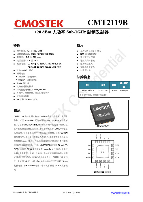
+20 dBm 大功率Sub-1GHz 射频发射器特性 ⏹ ⏹ ⏹ ⏹ ⏹ ⏹ ⏹ ⏹ ⏹ ⏹ ⏹ ⏹ ⏹ 应用于QFN16 (3X 3)17GNDCSB FCSB X IX OG P I O 2G P I O 1NC NC 13141516121112目录1.电气特性 (4)1.1推荐运行条件 (4)1.2绝对最大额定值 (4)1.3功耗 (5)1.4发射机 (5)1.5稳定时间 (6)1.6频率综合器 (6)1.7低电压检测 (6)1.8晶体 (7)1.9低频振荡器 (7)1.10数字接口 (7)1.11典型参数图表 (8)2.管脚描述 (10)3.典型应用原理图 (11)4.功能描述 (12)4.1发射器 (12)4.2辅助模块 (12)4.2.1晶体振荡器 (12)4.2.2睡眠计时器 (13)4.2.3低电压检测 (13)4.2.4快速手动跳频 (13)5.芯片运行 (14)5.1SPI接口 (14)5.2FIFO (14)5.2.1FIFO 读操作 (14)5.2.2FIFO 写操作 (15)5.2.3FIFO 相关中断 (15)5.3工作状态,时序及功耗 (16)5.3.1启动时序 (16)5.3.2工作状态 (16)5.4GPIO和中断 (18)6.数据包及包处理机 (20)6.1数据包格式 (20)6.2数据模式 (20)6.2.1直通模式 (21)6.2.2包模式 (21)7.自动运行模式 (22)8.用户寄存器 (23)8.1CMT区 (23)8.2系统区 (24)8.3频率区 (24)8.4数据率区 (24)8.5基带区 (25)8.6发射区 (25)8.7控制1区 (25)8.8控制2区 (26)9.订购信息 (27)10.封装信息 (28)11.顶部丝印 (29)11.1CMT2119B顶部丝印 (29)12.其它文档 (30)13.文档变更记录 (31)14.联系信息 (32)1. 电气特性V DD = 3.3 V,T OP = 25 °C,F RF = 433.92 MHz。
CD4011中文使用说明书

VO=4.6V,VI=0 或 5V 输出高电平电流 输出高电平电流 输入漏电流 -IOH -IOH ±IIN VO=9.5V,VI=0 或 10V VO=13.5V,VI=0 或 15V VO=2.5V,VI=0 或 5V VIN=0 或 15V
VDD=5V VDD=10V VDD=15V VDD=5V VDD=15V
V
输出低电平电流
VO=1.5V,VI=0 或 15V VO=4.6V,VI=0 或 5V 输出高电平电流 输出高电平电流 输入漏电流 -IOH -IOH VO=9.5V,VI=0 或 10V VO=2.5V,VI=0 或 5V VIN=0 或 15V
or
1.4 ±IIN VDD=15V 符号 测 试 条 件 最小 典型 IDD VI=VSS 或 VDD;IO=0 VI=VSS 或 VDD, ∣IO∣<1µA VOL VOH VI=VSS 或 VDD, ∣IO∣<1µA VDD=5V VDD=10V VDD=15V VDD=5V VDD=10V VDD=15V VDD=5V VDD=10V VDD=15V VDD=5V VDD=10V VDD=15V VDD=5V VDD=10V VDD=15V VDD=5V VDD=10V VDD=15V 3.5 7.0 11.0 0.52 1.3 3.6 4.95 9.95 14.95 VO=0.5V 或 4.5V,∣IO∣<1µA VO=1.0V 或 9.0V,∣IO∣<1µA VO=1.5V 或 13.5V,∣IO∣<1µA VO=0.5V 或 4.5V,∣IO∣<1µA VO=1.0V 或 9.0V,∣IO∣<1µA VO=1.5V 或 13.5V,∣IO∣<1µA VO=0.4V,VI=0 或 5V
SA1117C 1A中文资料
SA1117C1A LDO 稳压器电路概述SA1117C是一款正电压输出的低压降三端线性稳压电 路,在1A输出电流下压降为1.2V。
SA1117C分为两个版本:固定电压输出版本和可调电 压 输 出 版 本 , 固 定 输 出 电 压 为 1.5V , 1.8V , 2.5V , 3.3V , 5.0V 和可调版本的电压精度为 1.5% ,固定电压为 1.2V的产品输出电压精度为2%。
SA1117C内部集成过热保护和限流电路,适用于各类 电子产品。
TO-252-2L SOT-223-3L特点* 固定输出电压为 1.5V,1.8V,2.5V, 3.3V,5.0V 和 可调版本的电压输出精度为 1.5%; * 固定电压为 1.2V 的输出精度为 2% * 低压降电压:1A 输出电流时仅为 1.2V * 限流功能 * 过热切断 * 温度范围:-40°C~ 125°C应用* 膝上型电脑,掌上电脑和笔记本 电脑 * 电池充电器 * SCSI-II 主动终端 * 移动电话 * 无绳电话 * 电池供电系统 * 便携式设备 * 开关电源的后置稳压器产品规格分类(温度范围:-40°C ~ 125°C)杭州士兰微电子股份有限公司版本号:1.02010.05.14 共9页 第1页SA1117C产品名称 SA1117CH-ADJTR SA1117CH-1.2TR SA1117CH-1.5TR SA1117CH-1.8TR SA1117CH-2.5TR SA1117CH-3.3TR SA1117CH-5.0TR SA1117CD-ADJ SA1117CD-ADJTR SA1117CD-1.2 SA1117CD-1.2TR SA1117CD-1.5 SA1117CD-1.5TR SA1117CD-1.8 SA1117CD-1.8TR SA1117CD-2.5 SA1117CD-2.5TR SA1117CD-3.3 SA1117CD-3.3TR SA1117CD-5.0 SA1117CD-5.0TR TO-252-2L SOT-223-3L 封 装 打印名称 SA1117CH-ADJ SA1117CH-1.2 SA1117CH-1.5 SA1117CH-1.8 SA1117CH-2.5 SA1117CH-3.3 SA1117CH-5.0 SA1117CD-ADJ SA1117CD-ADJ SA1117CD-1.2 SA1117CD-1.2 SA1117CD-1.5 SA1117CD-1.5 SA1117CD-1.8 SA1117CD-1.8 SA1117CD-2.5 SA1117CD-2.5 SA1117CD-3.3 SA1117CD-3.3 SA1117CD-5.0 SA1117CD-5.0 材料 无铅 无铅 无铅 无铅 无铅 无铅 无铅 无铅 无铅 无铅 无铅 无铅 无铅 无铅 无铅 无铅 无铅 无铅 无铅 无铅 无铅 包装 编带 编带 编带 编带 编带 编带 编带 料管 编带 料管 编带 料管 编带 料管 编带 料管 编带 料管 编带 料管 编带杭州士兰微电子股份有限公司版本号:1.02010.05.14 共9页 第2页SA1117C内部框图3VINTSDCurrent Limit VOUT Fixed: F1 and F2 connect, disconnect A F2 A Adj: A connect, F1 and F2 disconnect 1 ADJ/GNDBandGap F12极限参数参 输入工作电压 引脚温度 (焊接5秒) 工作结温范围 储存温度 功耗 ESD能力 (最小值) 数 符号 VIN TLead TJ Tstg PD ESD 范 围 单位 V °C °C °C mW V15 260 150 -65 ~ +150 内部限制 (注1) 2000注1:最大允许功耗是最大工作结温TJ (max),结对空热阻θJA 和环境温度Tamb的函数。
UPD703031AYGC中文资料
Document No. U14734EJ1V0DS00 (1st edition)Date Published April 2000 N CP(K)Printed in Japan©2000{Serial interface•Asynchronous serial interface (UART0, UART1)•Clocked serial interface (CSI0 to CSI3)•3-wire variable length serial interface (CSI4)•I2C bus interface (I2C0, I2C1) (µPD703031AY, 703033AY, 70F3033AY only){10-bit resolution A/D converter: 12 channels{DMA controller: 6 channels{Real-time output port: 8 bits × 1 channel or 4 bits × 2 channels{ROM correction: 4 places can be corrected{Power-saving function: HALT/IDLE/STOP modes{Packages: 100-pin plastic LQFP (fine pitch) (14 × 14)100-pin plastic QFP (14 × 20){µPD70F3033A, 70F3033AY•Can be replaced with µPD703033A and 703033AY (internal mask ROM) in mass productionAPPLICATIONS{AV equipment (audio, car audio, VCR, TV, etc.)ORDERING INFORMATIONPart Number Package Internal ROMµPD703031AGC-×××-8EU µPD703031AYGC-×××-8EU µPD703031AGF-×××-3BA µPD703031AYGF-×××-3BA µPD703033AGC-×××-8EU µPD703033AYGC-×××-8EU µPD703033AGF-×××-3BA µPD703033AYGF-×××-3BA µPD70F3033AGC-8EU Note µPD70F3033AYGC-8EU Note µPD70F3033AGF-3BA Note µPD70F3033AYGF-3BA Note 100-pin plastic LQFP (fine pitch) (14 × 14)100-pin plastic LQFP (fine pitch) (14 × 14)100-pin plastic QFP (14 × 20)100-pin plastic QFP (14 × 20)100-pin plastic LQFP (fine pitch) (14 × 14)100-pin plastic LQFP (fine pitch) (14 × 14)100-pin plastic QFP (14 × 20)100-pin plastic QFP (14 × 20)100-pin plastic LQFP (fine pitch) (14 × 14)100-pin plastic LQFP (fine pitch) (14 × 14)100-pin plastic QFP (14 × 20)100-pin plastic QFP (14 × 20)Mask ROM (128 KB)Mask ROM (128 KB)Mask ROM (128 KB)Mask ROM (128 KB)Mask ROM (256 KB)Mask ROM (256 KB)Mask ROM (256 KB)Mask ROM (256 KB)Flash memory (256 KB)Flash memory (256 KB)Flash memory (256 KB)Flash memory (256 KB)Note Under developmentRemarks1.××× indicates ROM code suffix.2.ROMless versions are not provided.Data Sheet U14734EJ1V0DS00 2PIN CONFIGURATION (Top View)100-pin plastic LQFP (fine pitch) (14 × 14)•µPD703031AGC-×××-8EU•µPD70F3033AGC-8EU•µPD703031AYGC-×××-8EU•µPD70F3033AYGC-8EU•µPD703033AGC-×××-8EU•µPD703033AYGC-×××-8EUData Sheet U14734EJ1V0DS003100-pin plastic QFP (14 × 20)•µPD703031AGF-×××-3BA•µPD70F3033AGF-3BA •µPD703031AYGF-×××-3BA•µPD70F3033AYGF-3BA •µPD703033AGF-×××-3BA•µPD703033AYGF-×××-3BA4Data Sheet U14734EJ1V0DS00PIN IDENTIFICATIONA1 to A21:Address Bus P80 to P83:Port 8AD0 to AD15:Address/Data Bus P90 to P96:Port 9ADTRG:AD Trigger Input P100 to P107:Port 10ANI0 to ANI11:Analog Input P110 to P113:Port 11ASCK0, ASCK1:Asynchronous Serial Clock RD:ReadASTB:Address Strobe REGC:Regulator ClockAV DD:Analog Power Supply RESET:ResetAV REF:Analog Reference Voltage RTP0 to RTP7:Real-time Output PortAV SS:Analog Ground RTPTRG:RTP Trigger InputBV DD:Power Supply for Bus Interface R/W:Read/Write StatusBV SS:Ground for Bus Interface RXD0, RXD1:Receive DataCLKOUT:Clock Output SCK0 to SCK4:Serial ClockDSTB:Data Strobe SCL0, SCL1:Serial ClockEV DD:Power Supply for Port SDA0, SDA1:Serial DataEV SS:Ground for Port SI0 to SI4:Serial InputHLDAK:Hold Acknowledge SO0 to SO4:Serial OutputHLDRQ:Hold Request TI00, TI01, TI10, :Timer InputIC:Internally Connected TI11, TI2 to TI5INTP0 to INTP6:Interrupt Request from Peripherals TO0 to TO5:Timer OutputKR0 to KR7:Key Return TXD0, TXD1:Transmit DataLBEN:Lower Byte Enable UBEN:Upper Byte EnableNMI:Non-Maskable Interrupt Request V DD:Power SupplyP00 to P07:Port 0V PP:Programming Power SupplyP10 to P15:Port 1V SS:GroundP20 to P27:Port 2WAIT:WaitP30 to P37:Port 3WRH:Write Strobe High Level DataP40 to P47:Port 4Write Strobe Low Level DataP50 to P57:Port 5X1, X2:Crystal for Main ClockP60 to P65:Port 6XT1, XT2:Crystal for Sub-clockP70 to P77:Port 7Data Sheet U14734EJ1V0DS005INTERNAL BLOCK DIAGRAM6Data Sheet U14734EJ1V0DS00CONTENTS1.DIFFERENCES AMONG PRODUCTS (8)1.1Differences of µPD703031A, 703031AY, 703033A, 703033AY, 70F3033A, and 70F3033AY (8)2.PIN FUNCTIONS (9)2.1Port Pins (9)2.2Non-Port Pins (11)2.3Pin I/O Circuits and Recommended Connection of Unused Pins (15)3.PROGRAMMING FLASH MEMORY (µPD70F3033A, 70F3033AY ONLY) (19)3.1Selecting Communication Mode (19)3.2Function of Flash Memory Programming (20)3.3Connecting Dedicated Flash Programmer (20)4.ELECTRICAL SPECIFICATIONS (22)4.1Flash Memory Programming Mode (µPD70F3033A, 70F3033AY only) (47)5.PACKAGE DRAWINGS (48)6.RECOMMENDED SOLDERING CONDITIONS (50)Data Sheet U14734EJ1V0DS0071.DIFFERENCES AMONG PRODUCTS1.1Differences of µPD703031A, 703031AY, 703033A, 703033AY, 70F3033A, and 70F3033AYCautions 1.There are differences in noise immunity and noise radiation between the flash memory and mask ROM versions. When pre-producing an application set with the flash memory versionand then mass-producing it with the mask ROM version, be sure to conduct sufficientevaluations for the commercial samples (not engineering samples) of the mask ROMversion.2.When replacing the flash memory versions with mask ROM versions, write the same codein the empty area of the internal ROM.8Data Sheet U14734EJ1V0DS002.PIN FUNCTIONS2.1Port PinsRemark PULL: On-chip pull-up resistorData Sheet U14734EJ1V0DS009Data Sheet U14734EJ1V0DS0010Remark PULL: On-chip pull-up resistor2.2Non-Port PinsRemark PULL: On-chip pull-up resistorRemark PULL: On-chip pull-up resistorRemark PULL: On-chip pull-up resistorRemark PULL: On-chip pull-up resistor2.3Pin I/O Circuits and Recommended Connection of Unused PinsThe input/output circuit type of each pin and recommended connection of unused pins are show in Table 2-1. For the input/output schematic circuit diagram of each type, refer to Figure 2-1.Table 2-1. Types of Pin I/O Circuits (1/2)Table 2-1. Types of Pin I/O Circuits (2/2)Notes1.µPD703031A, 703031AY, 703033A, 703033AY2.µPD70F3033A, 70F3033AYCaution Three power supply systems are available to supply power to the I/O buffers of the V850/SB1’s pins: EV DD, BV DD, and AV DD. The voltage ranges that can be used for these I/O buffer power supplies are shown below.EV DD, BV DD: 3.0 V to 5.5 VAV DD: 4.5 V to 5.5 VThe electrical specifications differ depending on whether the power supply voltage range is 3.0 V to under 4.0 V, or 4.0 V to 5.5 V.Figure 2-1. Pin Input/Output Circuits (1/2)Caution V DD in the circuit diagrams can be read as EV DD, BV DD, or AV DD, as appropriate.Figure 2-1. Pin Input/Output Circuits (2/2)Caution V DD in the circuit diagrams can be read as EV DD, BV DD, or AV DD, as appropriate.3.PROGRAMMING FLASH MEMORY (µPD70F3033A, 70F3033AY ONLY)There are the following two methods for writing a program to the flash memory.(1)On-board programmingWrite a program to the flash memory using a dedicated flash programmer after the µPD70F3033A and 70F3033AY have been mounted on the target board. Also mount a connector, etc. on the target board to communicate with the dedicated flash programmer.(2)Off-board programmingWrite a program using a dedicated adapter before the µPD70F3033A and 70F3033AY have been mounted on the target board.3.1Selecting Communication ModeTo write the flash memory, use a dedicated flash programmer and serial communication. Select a serial communication mode from those listed in Table 3-1 in the format shown in Figure 3-1. Each communication mode is selected by the number of V PP pulses shown in Table 3-1.Table 3-1. Communication ModesFigure 3-1. Communication Mode Selecting Format3.2Function of Flash Memory ProgrammingOperations such as writing to flash memory are performed by various command/data transmission and reception operations according to the selected communication mode. The major functions are shown below.Table 3-2. Major Functions of Flash Memory ProgrammingFunctionCategory Command DescriptionVerify Batch verify Compares the contents of the entire memory and the input data.Batch erase Erases the contents of the entire memory.EraseWrite backWrites back the contents which is overerased.Blank check Batch blank check Checks the erase state of the entire memory.High-speed writeWrites data by the specification of the write start address and thenumber of bytes to be written, and executes verify check.Data writeContinuous writeWrites data from the address following the high-speed write command executed immediately before, and executes verify check.Status read out Reads out the status of operations.Oscillation frequency settingSets the oscillation frequency.Erase time setting Sets the erase time of batch erase.Write time setting Sets the write time of data write.Write back time setting Sets the write back time.Baud rate setting Sets the baud rate when using UART0.Silicon signature Reads out the silicon signature information.Systemsetting/controlResetRestarts the system of flash programmer.3.3Connecting Dedicated Flash ProgrammerThe connection of the dedicated flash programmer and the µPD70F3033A and 70F3033AY differs according to the communication mode. The connections for each communication mode are shown below.Figure 3-2. Connection of Dedicated Flash Programmer in CSI0 ModeFigure 3-3. Connection of Dedicated Flash Programmer in CSI0 + HS Mode4.ELECTRICAL SPECIFICATIONSAbsolute Maximum Ratings (T A = 25°C, V SS = 0 V)Parameter Symbol Conditions Ratings UnitV DD V DD pin–0.5 to +7.0VAV DD AV DD pin–0.5 to +7.0VBV DD BV DD pin–0.5 to +7.0VEV DD EV DD pin–0.5 to +7.0VAV SS AV SS pin–0.5 to +0.5VBV SS BV SS pin–0.5 to +0.5V Supply voltageEV SS EV SS pin–0.5 to +0.5VV I1Note 1 (BV DD pin)–0.5 to BV DD + 0.5Note 4VV I2Note 2 (EV DD pin)–0.5 to EV DD + 0.5Note 4V Input voltageV I3V PP pin (µPD70F3033A, 70F3033AY only)–0.5 to +8.5V Analog input voltage V IAN Note 3 (AV DD pin)–0.5 to AV DD + 0.5Note 4V Analog reference input voltage AV REF AV REF pin–0.5 to AV DD + 0.5Note 4VPer pin 4.0mATotal for P00 to P07, P10 to P15, P20 toP2525mATotal for P26, P27, P30 to P37, P100 toP107, P110 to P11325mATotal for P40 to P47, P90 to P96, CLKOUT25mA Output current, low I OLTotal for P50 to P57, P60 to P6525mAPer pin–4.0mATotal for P00 to P07, P10 to P15, P20 toP25–25mATotal for P26, P27, P30 to P37, P100 toP107, P110 to P113–25mATotal for P40 to P47, P90 to P96, CLKOUT–25mA Output current, high I OHTotal for P50 to P57, P60 to P65–25mAV O1Note 1 (BV DD pin)–0.5 to BV DD + 0.5Note 4V Output voltageV O2Note 2 (EV DD pin)–0.5 to EV DD + 0.5Note 4VNormal operation mode–40 to +85°C Operating ambient temperature T AFlash memory programming mode(µPD70F3033A, 70F3033AY only)10 to 85°CµPD703031A, 703031AY µPD703033A, 703033AY –65 to +150°CStorage temperature T stgµPD70F3033A, 70F3033AY–40 to +125°C Notes1.Ports 4, 5, 6, 9, CLKOUT, and their alternate-function pins2.Ports 0, 1, 2, 3, 10, 11, RESET, and their alternate-function pins3.Ports 7, 8, and their alternate-function pins4.Be sure not to exceed the absolute maximum ratings (MAX. value) of each supply voltage.Cautions1.Do not directly connect the output (or I/O) pins of IC products to each other, or to V DD , V CC ,and GND. Open-drain pins or open-collector pins, however, can be directly connected to each other. Direct connection of the output pins between an IC product and an external circuit is possible, if the output pins can be set to the high-impedance state and the output timing of the external circuit is designed to avoid output conflict.2.Product quality may suffer if the absolute maximum rating is exceeded even momentarily for any parameter. That is, the absolute maximum ratings are rated values at which the product is on the verge of suffering physical damage, and therefore the product must be used under conditions that ensure that the absolute maximum ratings are not exceeded.The ratings and conditions indicated for DC characteristics and AC characteristics represent the quality assurance range during normal operation.Capacitance (T A = 25°C)ParameterSymbol ConditionsMIN.TYP.MAX.Unit Input capacitance C I 15pF I/O capacitance C IO 15pF Output capacitanceC Of C = 1 MHzUnmeasured pins returned to 0 V15pFOperating Conditions (1)Operating frequencyOperating Frequency (f XX )V DD AV DD BV DD EV DD Remark 2 to 20 MHz 4.0 to 5.5 V 4.5 to 5.5 V 4.0 to 5.5 V 4.0 to 5.5 V Note 12 to 17 MHz 4.0 to 5.5 V 4.5 to 5.5 V 3.0 to 5.5 V 3.0 to 5.5 V Note 1Other than IDLE mode 4.0 to 5.5 V 4.5 to 5.5 V 3.0 to 5.5 V 3.0 to 5.5 V –32.768 kHzIDLE mode3.5 to 5.5 V4.5 to5.5 V3.0 to 5.5 V3.0 to 5.5 VNote 2Notes 1.During STOP mode (subsystem oscillator operating), V DD = 3.5 to 5.5 V. Shifting to STOP mode orrestoring from STOP mode must be performed at V DD = 4.0 V min.2.Shifting to IDLE mode or restoring from IDLE mode must be performed at V DD = 4.0 V min.(2)CPU operating frequencyParameterSymbol ConditionsMIN.TYP.MAX.Unit Main system clock operation 0.2520MHz CPU operating frequencyf CPUSubsystem clock operation32.768kHzRecommended Oscillator(1)Main system clock oscillator (T A = –40 to +85°C)(a)Connection of ceramic resonator or crystal resonator(2)Subsystem clock oscillator (T A = –40 to +85°C)(a)Connection of crystal resonatorDC Characteristics(T A = –40 to +85°C, V DD = 4.0 to 5.5 V, BV DD = EV DD = 3.0 to 5.5 V, AV DD = 4.5 to 5.5 V, V SS = AV SS = BV SS = EV SS = 0 V)4.Ports 7, 8, and their alternate-function pinsDC Characteristics(T A = –40 to +85°C, V DD = 4.0 to 5.5 V, BV DD = EV DD = 3.0 to 5.5 V, AV DD = 4.5 to 5.5 V, V SS = AV SS = BV SS = EV SS = 0 V) Parameter Symbol Conditions MIN.TYP.MAX.Unit µPD703031A,I DD1In normal operation mode Note 12540mAµPD703031AY,I DD2In HALT mode Note 11020mAµPD703033A,I DD3In IDLEmode Note 2Watch timer operating14mAWatch timer, subsystem oscillator operating 1370µAI DD4In STOPmodeSubsystem oscillatorstopped, XT1 = V SS870µAI DD5In normal mode (subsystemoperation)Note 350150µAµPD703033AYI DD6In IDLE mode (subsystemoperation)Note 31370µA µPD70F3033A,I DD1In normal operation mode Note 13360mAI DD2In HALT mode Note 11020mAI DD3In IDLEmode Note 2Watch timer operating14mAWatch timer, subsystem oscillator operating 13100µAI DD4In STOPmodeSubsystem oscillatorstopped, XT1 = V SS8100µAI DD5In normal mode (subsystemoperation)Note 3200600µASupply currentµPD70F3033AYI DD6In IDLE mode (subsystemoperation)Note 390180µAPull-up resistance R L V IN = 0 V1030100kΩNotes 1.f CPU = f XX = 20 MHz, all peripheral functions operating, output buffer: OFF2.f XX = 20 MHz3.f CPU = f XT = 32.768 kHz, main system clock oscillator stoppedRemark TYP. values are reference values for when T A = 25°C, V DD = BV DD = EV DD = AV DD = 5.0 V. The current consumed by the output buffer is not included.Data Retention Characteristics (T A = –40 to +85°C)ParameterSymbol ConditionsMIN.TYP.MAX.Unit Data retention voltage V DDDR STOP mode 3.0Note5.5VµPD703031A,µPD703031AY,µPD703033A,µPD703033AY 870µAData retention currentI DDDRV DD = V DDDR ,XT1 = V SS (subsystem stopped)µPD70F3033A,µPD70F3033AY8100µA Supply voltage rise time t RVD 200µs Supply voltage fall time t FVD 200µs Supply voltage hold time (from STOP mode setting)t HVD 0ms STOP release signal input time t DREL 0msData retention high-level input voltage V IHDR All input ports 0.9V DDDRV DDDR V Data retention low-level input voltageV ILDRAll input ports0.1V DDDRVNote During STOP mode (subsystem oscillator operating), V DD = 3.5 to 5.5 V. Shifting to STOP mode or restoring from STOP mode must be performed at V DD = 4.0 V min.Remark TYP. values are reference values for when T A = 25°C.AC Characteristics (T A = –40 to +85°C, V DD = 4.0 to 5.5 V, BV DD = EV DD = 3.0 to 5.5 V, AV DD = 4.5 to 5.5 V, V SS = AV SS = BV SS = EV SS = 0 V)AC Test Input Waveform (V DD: EV DD, BV DD, AV DD))AC Test Output Test Points (EV DD, BV DDLoad Conditions(1)Clock timing(a)T A = –40 to +85°C, V DD = BV DD = 4.0 to 5.5 V, V SS = BV SS = 0 VParameterSymbol ConditionsMIN.MAX.UnitCLKOUT output cycle <1>t CYK 50 ns 31.2 µsCLKOUT high-level width <2>t WKH 0.4t CYK – 12ns CLKOUT low-level width <3>t WKL 0.4t CYK – 12ns CLKOUT rise time <4>t KR 12ns CLKOUT fall time<5>t KF12ns (b)T A = –40 to +85°C, V DD = 4.0 to 5.5 V, BV DD = 3.0 to 4.0 V, V SS = BV SS = 0 VParameterSymbol ConditionsMIN.MAX.UnitCLKOUT output cycle <1>t CYK 58.8 ns 31.2 µsCLKOUT high-level width <2>t WKH 0.4t CYK – 15ns CLKOUT low-level width <3>t WKL 0.4t CYK – 15ns CLKOUT rise time <4>t KR 15ns CLKOUT fall time<5>t KF15ns(2)Output waveform (other than port 4, port 5, port 6, port 9, X1, and CLKOUT)(T A = –40 to +85°C, V DD = 4.0 to 5.5 V, BV DD = EV DD = 3.0 to 5.5 V, V SS = BV SS = EV SS = 0 V) Parameter Symbol Conditions MIN.MAX.Unit Output rise time<6>t OR20ns Output fall time<7>t OF20ns(3)Reset timing(4)Bus timing(a)Clock asynchronous (T A = –40 to +85°C, V DD = BV DD = 4.0 to 5.5 V, V SS = BV SS = 0 V)Remarks1.T = 1/f CPU (f CPU: CPU clock frequency)2.n: Number of wait clocks inserted in the bus cycle.The sampling timing changes when a programmable wait is inserted.3.The values in the above specifications are values for when clocks with a 5:5 duty ratio are input fromX1.(b)Clock asynchronous (T A = –40 to +85°C, V DD = 4.0 to 5.5 V, BV DD = 3.0 to 4.0 V, V SS = BV SS = 0 V)Remarks1.T = 1/f CPU (f CPU: CPU clock frequency)2.n: Number of wait clocks inserted in the bus cycle.The sampling timing changes when a programmable wait is inserted.3.The values in the above specifications are values for when clocks with a 5:5 duty ratio are input fromX1.(c)Clock synchronous (T A = –40 to +85°C, V DD = BV DD = 4.0 to 5.5 V, V SS = BV SS = 0 V)Remark The values in the above specifications are values for when clocks with a 5:5 duty ratio are input from X1.(e)Read cycle (CLKOUT synchronous/asynchronous, 1 wait)(f)Write cycle (CLKOUT synchronous/asynchronous, 1 wait)(g)Bus hold timing(5)Interrupt timing(T A = –40 to +85°C, V DD = 4.0 to 5.5 V, EV DD = 3.0 to 5.5 V, V SS = AV SS = BV SS = EV SS = 0 V)ParameterSymbol ConditionsMIN.MAX.Unit NMI high-level width <51>t WNIH 500ns NMI low-level width <52>t WNIL 500ns n = 0 to 3, analog noise elimination500ns n = 4, 5, digital noise elimination 3T + 20ns INTPn high-level width<53>t WITHn = 6, digital noise elimination3Tsmp + 20ns n = 0 to 3, analog noise elimination500ns n = 4, 5, digital noise elimination 3T + 20ns INTPn low-level width<54>t WITLn = 6, digital noise elimination3Tsmp + 20nsRemarks 1.T = 1/f XX2.Tsmp = Noise elimination sampling clock cycle(6)RPU timing (T A = –40 to +85°C, V DD = 4.0 to 5.5 V, EV DD = 3.0 to 5.5 V, V SS = AV SS = BV SS = EV SS = 0 V)Parameter Symbol Conditions MIN.MAX.UnitTIn0, TIn1 high-level width<55>t TIHn n = 0, 12T sam + 20Note nsTIn0, TIn1 low-level width<56>t TILn n = 0, 12T sam + 20Note nsTIn high-level width<57>t TIHn n = 2 to 53T + 20nsTIn low-level width<58>t TILn n = 2 to 53T + 20ns Note T sam can select the following count clocks by setting the PRMn2 to PRMn0 bits of prescaler mode registers n0, n1 (PRMn0, PRMn1).When n = 0 (TM0), T sam = 2T, 4T, 16T, 64T, 256T, or 1/INTWTNI cycleWhen n = 1 (TM1), T sam = 2T, 4T, 16T, 32T, 128T, or 256THowever, when the TIn0 valid edge is selected as the count clock, T sam = 4T.Remark T = 1/f XX(7)Asynchronous serial interface (UART0, UART1) timing(T A = –40 to +85°C, V DD = 4.0 to 5.5 V, EV DD = 3.0 to 5.5 V, V SS = EV SS = 0 V)Parameter Symbol Conditions MIN.MAX.Unit ASCKn cycle time<59>t KCY13200ns ASCKn high-level width<60>t KH1380ns ASCKn low-level width<61>t KSO1380ns Remark n = 0, 1(8)3-wire serial interface (CSI0 to CSI3) timing(a)Master mode (T A = –40 to +85°C, V DD = 4.0 to 5.5 V, EV DD = 3.0 to 5.5 V, V SS = EV SS = 0 V)Remark n = 0 to 3(9)3-wire variable length serial interface (CSI4) timing(a)Master mode (T A = –40 to +85°C, V DD = 4.0 to 5.5 V, EV DD = 3.0 to 5.5 V, V SS = EV SS = 0 V)(10)I2C bus mode (µPD703031AY, 703033AY, 70F3033AY only)(T A = –40 to +85°C, V DD = 4.0 to 5.5 V, EV DD = 3.0 to 5.5 V, V SS = EV SS = 0 V)Normal Mode High-Speed Mode Parameter SymbolMIN.MAX.MIN.MAX.UnitSCLn clock frequency–f CLK01000400kHz Bus-free time (betweenstop/start conditions)<74>t BUF 4.7– 1.3–µsHold time Note 1<75>t HD:STA 4.0–0.6–µs SCLn clock low-level width<76>t LOW 4.7– 1.3–µs SCLn clock high-level width<77>t HIGH 4.0–0.6–µs Setup time for start/restartconditions<78>t SU:STA 4.7–0.6–µsCBUS compatible master 5.0–––µsData holdtimeI2C mode <79>t HD:DAT0Note 2–0Note 20.9Note 3µsData setup time<80>t SU:DAT250–100Note 4–nsSDAn and SCLn signal risetime<81>t R–100020 + 0.1Cb Note 5300nsSDAn and SCLn signal falltime<82>t F–30020 + 0.1Cb Note 5300ns Stop condition setup time<83>t SU:STO 4.0–0.6–µs Pulse width of spikesuppressed by input filter<84>t SP––050nsCapacitance load of eachbus line–Cb–400–400pFNotes1.At the start condition, the first clock pulse is generated after the hold time.2.The system requires a minimum of 300 ns hold time internally for the SDAn signal (at V IHmin..of SCLn signal) in order to occupy the undefined area at the falling edge of SCLn.3.If the system does not extend the SCLn signal low hold time (t LOW), only the maximum data hold time(t HD:DAT) needs to be satisfied.4.The high-speed mode I2C bus can be used in the normal-mode I2C bus system. In this case, set thehigh-speed mode I2C bus so that it meets the following conditions.•If the system does not extend the SCLn signal’s low state hold time:t HD:DAT≥ 250 ns•If the system extends the SCLn signal’s low state hold time:Transmit the following data bit to the SDAn line prior to the SCLn line release (t Rmax. + t SU:DAT = 1000+ 250 = 1250 ns: Normal mode I2C bus specification).5. Cb: Total capacitance of one bus line (unit: pF)Remark n = 0, 1A/D Converter Characteristics (T A = –40 to +85°C, V DD = AV DD = AV REF, V SS = AV SS = 0 V, Output pin load capacitance: C L = 50 pF)Parameter Symbol Conditions MIN.TYP.MAX.Unit Resolution–101010bit Overall error Note 1–ADM2 = 00H±0.6%FSRADM2 = 01H±1.0%FSR Conversion time t CONV510µs Zero-scale error Note 1AINL±0.4%FSR Full-scale error Note 1AINLADM2 = 00H±0.4%FSRADM2 = 01H±0.6%FSR Integral linearity error Note 2INLADM2 = 00H±4.0LSBADM2 = 01H±6.0LSB Differential linearity error Note 2DNLADM2 = 00H±4.0LSBADM2 = 01H±6.0LSB Analog reference voltage AV REF AV REF =AV DD 4.5 5.5V Analog power supply voltage AV DD 4.5 5.5V Analog input voltage V IAN AV SS AV REF V AV REF input current AI REF12mA AV DD current AI DDADM2 = 00H36mAADM2 = 01H48mA Notes1.Excluding quantization error (±0.05 %FSR)2.Excluding quantization error (±0.5 LSB)Remarks 1.LSB: Least Significant BitFSR: Full Scale Range2.ADM2: A/D converter mode register 2Regulator (T A = –40 to +85°C, V DD = 4.0 to 5.5 V, V SS = 0 V)Parameter Symbol Conditions MIN.TYP.MAX.Unit1Output stabilization time<85>t REG Stabilization capacitance C = 1 µFms(Connected to REGC pin)4.1Flash Memory Programming Mode (µPD70F3033A, 70F3033AY only)Basic characteristics (T A = 10 to 85°C)ParameterSymbol Conditions MIN.TYP.MAX.Unit Operating frequency f X 220MHz Power supply voltage V DD 4.55.5V I DDW V DD pin 63mA Write currentI PPWWhen V PP = V PP1V PP pin50mA I DDE V DD pin 63mA Erase currentI PPEWhen V PP = V PP1V PP pin100mA V PP0During normal operation00.6V V PP power supply voltageV PP1During flash memory programming7.57.88.1V Write countNoteC WRT 202020Times Unit erase time t ER 0.20.20.2s Total erase timet ERT5.8sNote Erase/write are regarded as 1 cycle.5.PACKAGE DRAWINGS100-PIN PLASTIC LQFP (FINE PITCH) (14x14)NOTEEach lead centerline is located within 0.08 mm ofits true position (T.P.) at maximum material condition.ITEM MILLIMETERS ABDG16.00±0.2014.00±0.200.50 (T.P.)1.00J16.00±0.20KC14.00±0.20I0.081.00±0.20L0.50±0.20F 1.00NPQ0.081.40±0.050.10±0.05S100GC-50-8EU-1 S 1.60 MAX.H0.22+0.05−0.04M0.17+0.03−0.07R3°+7°−3°detail of lead end100-PIN PLASTIC QFP (14x20)NOTEEach lead centerline is located within 0.15 mm ofits true position (T.P.) at maximum material condition.ITEM MILLIMETERS ABDG23.6±0.420.0±0.20.30±0.100.6H17.6±0.4IC14.0±0.20.15J0.65 (T.P.)K 1.8±0.2L0.8±0.2F0.8P100GF-65-3BA1-4 NPQ0.102.7±0.10.1±0.1R5°±5°S 3.0 MAX.M0.15+0.10−0.056.RECOMMENDED SOLDERING CONDITIONSThe µPD703031A, 703031AY, 703033A, 703033AY, 70F3033A, and 70F3033AY should be soldered and mounted under the following recommended conditions.For the details of the recommended soldering conditions, refer to the document Semiconductor Device Mounting Technology Manual (C10535E).For soldering methods and conditions other than those recommended below, contact your NEC sales representative.Table 6-1. Surface Mounting Type Soldering Conditions (1/2)(1) µPD703031AGC-×××-8EU:100-pin plastic LQFP (fine pitch) (14 × 14)µPD703031AYGC-×××-8EU:100-pin plastic LQFP (fine pitch) (14 × 14)µPD703033AGC-×××-8EU:100-pin plastic LQFP (fine pitch) (14 × 14)µPD703033AYGC-×××-8EU:100-pin plastic LQFP (fine pitch) (14 × 14)Soldering Method Soldering Conditions RecommendedConditionSymbol Infrared reflow Package peak temperature: 235°C, Time: 30 seconds max. (at 210°C or higher),IR35-107-2Count: Two times or lessExposure limit: 7 days Note (after that, prebake at 125°C for 10 hours)VPS Package peak temperature: 215°C, Time: 40 seconds max. (at 200°C or higher),VP15-107-2Count: Two times or lessExposure limit: 7 days Note (after that, prebake at 125°C for 10 hours)Partial heating Pin temperature: 300°C max., Time: 3 seconds max. (per pin row)–Note After opening the dry pack, store it at 25°C or less and 65% RH or less for the allowable storage period.Caution Do not use different soldering methods together (except for partial heating).(2)µPD70F3033AGC-8EU:100-pin plastic LQFP (fine pitch) (14 × 14)µPD70F3033AYGC-8EU:100-pin plastic LQFP (fine pitch) (14 × 14)Soldering Method Soldering Conditions RecommendedConditionSymbol Infrared reflow Package peak temperature: 235°C, Time: 30 seconds max. (at 210°C or higher),IR35-103-2Count: Two times or lessExposure limit: 3 days Note (after that, prebake at 125°C for 10 hours)VPS Package peak temperature: 215°C, Time: 40 seconds max. (at 200°C or higher),VP15-103-2Count: Two times or lessExposure limit: 3 days Note (after that, prebake at 125°C for 10 hours)Partial heating Pin temperature: 300°C max., Time: 3 seconds max. (per pin row)–Note After opening the dry pack, store it at 25°C or less and 65% RH or less for the allowable storage period.Caution Do not use different soldering methods together (except for partial heating).。
UPD23C16040BLGY-MJH中文资料
The information in this document is subject to change without notice. Before using this document, please confirm that this is the latest version.Not all products and/or types are available in every country. Please check with an NEC Electronics sales representative for availability and additional information.Document No. M15720EJ3V0DS00 (3rd edition)Date Published March 2003 NS CP(K)Printed in JapanDATA SHEETThe mark shows major revised points.2001DescriptionThe µPD23C16040BL and µPD23C16080BL are 16,777,216 bits mask-programmable ROM. The word organization is selectable (BYTE mode : 2,097,152 words by 8 bits, WORD mode : 1,048,576 words by 16 bits). The active levels of OE (Output Enable Input) can be selected with mask-option.The µPD23C16040BL and µPD23C16080BL are packed in 48-pin PLASTIC TSOP(I) and 44-pin PLASTIC SOP.Features• Word organization2,097,152 words by 8 bits (BYTE mode) 1,048,576 words by 16 bits (WORD mode)• Page access modeBYTE mode :8 byte random page access (µPD23C16040BL)16 byte random page access (µPD23C16080BL)WORD mode :4 word random page access (µPD23C16040BL)8 word random page access (µPD23C16080BL)• Operating supply voltage : V CC = 2.7 V to 3.6 VOperating supplyAccess time /Power supply current (Active mode)Standby current voltage Page access timemA (MAX.)(CMOS level input)V CCns (MAX.)µPD23C16040BLµPD23C16080BLµA (MAX.)3.0 V ± 0.3 V 90 / 254055303.3 V ± 0.3 V85 / 25Ordering InformationPart Number PackageµPD23C16040BLGY-xxx-MJH48-pin PLASTIC TSOP(I) (12 x 18) (Normal bent)µPD23C16040BLGY-xxx-MKH48-pin PLASTIC TSOP(I) (12 x 18) (Reverse bent)µPD23C16040BLGX-xxx Note44-pin PLASTIC SOP (15.24 mm (600))µPD23C16080BLGY-xxx-MJH48-pin PLASTIC TSOP(I) (12 x 18) (Normal bent)µPD23C16080BLGY-xxx-MKH48-pin PLASTIC TSOP(I) (12 x 18) (Reverse bent)µPD23C16080BLGX-xxx Note44-pin PLASTIC SOP (15.24 mm (600))Note Under development(xxx : ROM code suffix No.)2Data Sheet M15720EJ3V0DSPin Configurations/xxx indicates active low signal.48-pin PLASTIC TSOP(I) (12 x 18) (Normal bent)[ µPD23C16040BLGY-xxx-MJH ][ µPD23C16080BLGY-xxx-MJH ]WORD, /BYTEA16A15A14A13A12A11A10A9A8A19NCNCA18A17A7A6A5A4A3A2A1A0/CEGNDGNDO15, A−1O7O14O6O13O5O12O4V CCV CCNCO11O3O10O2O9O1O8O0/OE or OE or DCGNDGNDA0 to A19:Address inputsO0 to O7, O8 to O14:Data outputsO15, A–1:Data output 15 (WORD mode),LSB Address input (BYTE mode)WORD, /BYTE:Mode select/CE:Chip Enable/OE or OE:Output EnableV CC:Supply voltageGND:GroundNC Note:No ConnectionDC:Don’t CareNote Some signals can be applied because this pin is not connected to the inside of the chip.Remark Refer to Package Drawings for the 1-pin index mark.3Data Sheet M15720EJ3V0DS4Data Sheet M15720EJ3V0DS48-pin PLASTIC TSOP(I) (12 x 18) (Reverse bent)[ µPD23C16040BLGY-xxx-MKH ][ µPD23C16080BLGY-xxx-MKH ]WORD, /BYTE A16A15A14A13A12A11A10A9A8A19NC NC A18A17A7A6A5A4A3A2A1A0/CEGND GND O15, A −1O7O14O6O13O5O12O4V CC V CC NC O11O3O10O2O9O1O8O0/OE or OE or DCGND GNDA0 to A19:Address inputsO0 to O7, O8 to O14:Data outputsO15, A–1:Data output 15 (WORD mode),LSB Address input (BYTE mode)WORD, /BYTE :Mode select /CE :Chip Enable /OE or OE :Output Enable V CC :Supply voltage GND :Ground NC Note:No Connection DC:Don’t CareNote Some signals can be applied because this pin is not connected to the inside of the chip.Remark Refer to Package Drawings for the 1-pin index mark.44-pin PLASTIC SOP (15.24 mm (600)) [ µPD23C16040BLGX-xxx ][ µPD23C16080BLGX-xxx ]Marking SideNCA18A17A7A6A5A4A3A2A1A0/CEGND /OE or OE or DCO0O8O1O9O2O10O3O11NCA19A8A9A10A11A12A13A14A15A16 WORD, /BYTE GNDO15, A−1O7O14O6O13O5O12O4V CCA0 to A19:Address inputsO0 to O7, O8 to O14:Data outputsO15, A–1:Data output 15 (WORD mode),LSB Address input (BYTE mode)WORD, /BYTE:Mode select/CE:Chip Enable/OE or OE:Output EnableV CC:Supply voltageGND:GroundNC Note:No ConnectionDC:Don’t CareNote Some signals can be applied because this pin is not connected to the inside of the chip.Remark Refer to Package Drawings for the 1-pin index mark.5Data Sheet M15720EJ3V0DSInput / Output Pin FunctionsPin name Input / Output Function WORD, /BYTE Input The pin for switching WORD mode and BYTE mode.High level : WORD mode (1M-word by 16-bit)Low level : BYTE mode (2M-word by 8-bit)A0 to A19 (Address inputs)Input Address input pins.A0 to A19 are used differently in the WORD mode and the BYTE mode.WORD mode (1M-word by 16-bit)A0 to A19 are used as 20 bits address signals.BYTE mode (2M-word by 8-bit)A0 to A19 are used as the upper 20 bits of total 21 bits of address signal.(The least significant bit (A−1) is combined to O15.)O0 to O7, O8 to O14 (Data outputs)Output Data output pins.O0 to O7, O8 to O14 are used differently in the WORD mode and the BYTE mode.WORD mode (1M-word by 16-bit)The lower 15 bits of 16 bits data outputs to O0 to O14.(The most significant bit (O15) combined to A−1.)BYTE mode (2M-word by 8-bit)8 bits data outputs to O0 to O7 and also O8 to O14 are high impedance.O15, A−1(Data output 15, LSB Address input)Output, Input O15, A−1 are used differently in the WORD mode and the BYTE mode.WORD mode (1M-word by 16-bit)The most significant output data bus (O15).BYTE mode (2M-word by 8-bit)The least significant address bus (A−1)./CE(Chip Enable)Input Chip activating signal.When the OE is active, output states are following.High level : High-ZLow level : Data out/OE or OE or DC (Output Enable, Don't care)Input Output enable signal. The active level of OE is mask option. The active level of OE can be selected from high active, low active and Don’t care at order.V CC−Supply voltageGND−GroundNC−Not internally connected. (The signal can be connected.)6Data Sheet M15720EJ3V0DSBlock DiagramA0 A1 A2 A3 A4 A5 A6 A7 A8 A9 A10 A11 A12 A13 A14 A15 A16 A17 A18WORD, /BYTE /OE or OE or DC/CEA197Data Sheet M15720EJ3V0DSMask OptionThe active levels of output enable pin (/OE or OE or DC) are mask programmable and optional, and can be selected from among " 0 " " 1 " " x " shown in the table below.Option/OE or OE or DC OE active level0/OE L1OE Hx DC Don’t careOperation modes for each option are shown in the tables below.Operation mode (Option : 0)/CE/OE Mode Output stateL L Active Data outH High-ZH H or L Standby High-ZOperation mode (Option : 1)/CE OE Mode Output stateL L Active High-ZH Data outH H or L Standby High-ZOperation mode (Option : x)/CE DC Mode Output stateL H or L Active Data outH H or L Standby High-ZRemark L : Low level inputH : High level input8Data Sheet M15720EJ3V0DSElectrical SpecificationsAbsolute Maximum RatingsParameter Symbol Condition Rating Unit Supply voltage V CC–0.3 to +4.6V Input voltage V I–0.3 to V CC+0.3V Output voltage V O–0.3 to V CC+0.3V Operating ambient temperature T A–10 to +70°C Storage temperature T stg–65 to +150°C Caution Exposing the device to stress above those listed in Absolute Maximum Ratings could cause permanent damage. The device is not meant to be operated under conditions outside the limitsdescribed in the operational section of this specification. Exposure to Absolute Maximum Ratingconditions for extended periods may affect device reliability.Capacitance (T A = 25 °C)Parameter Symbol Test condition MIN.TYP.MAX.Unit Input capacitance C I f = 1 MHz10pFOutput capacitance C O12pFDC Characteristics (T A = –10 to +70 °C, V CC = 2.7 to 3.6 V)Parameter Symbol Test conditions MIN.TYP.MAX.Unit High level input voltage V IH 2.0V CC + 0.3V Low level input voltage V IL V CC= 3.0 V ± 0.3 V–0.3+0.5VV CC= 3.3 V ± 0.3 V–0.3+0.8High level output voltage V OH I OH= –100 µA 2.4V Low level output voltage V OL I OL= 2.1 mA0.4V Input leakage current I LI V I= 0 V to V CC–10+10µA Output leakage current I LO V O= 0 V to V CC, Chip deselected–10+10µA Power supply current I CC1/CE= V IL (ActiveµPD23C16040BL V CC= 3.0 V ± 0.3 V40mAmode), I O= 0 mA V CC= 3.3 V ± 0.3 V40µPD23C16080BL V CC= 3.0 V ± 0.3 V55V CC= 3.3 V ± 0.3 V55Standby current I CC3/CE= V CC – 0.2 V (Standby mode)30µA9Data Sheet M15720EJ3V0DS10Data Sheet M15720EJ3V0DSAC Characteristics (T A = –10 to +70 °C, V CC = 2.7 to 3.6 V)ParameterSymbolTest conditionV CC = 3.0 V ± 0.3 V V CC = 3.3 V ± 0.3 V UnitMIN.TYP.MAX.MIN.TYP.MAX.Address access timet ACC 9085ns Page access time t PAC 2525ns Address skew time t SKEW Note1010ns Chip enable access time t CE 9085ns Output enable access time t OE 2525ns Output hold time t OH 00ns Output disable time t DF 025025ns WORD, /BYTE access timet WB9085ns Note t SKEW indicates the following three types of time depending on the condition.1) When switching /CE from high level to low level, t SKEW is the time from the /CE low level input point until the next address is determined.2) When switching /CE from low level to high level, t SKEW is the time from the address change start point to the /CE high level input point.3) When /CE is fixed to low level, t SKEW is the time from the address change start point until the next address is determined.Since specs are defined for t SKEW only when /CE is active, t SKEW is not subject to limitations when /CE is switched from high level to low level following address determination, or when the address is changed after /CE is switched from low level to high level.Remarkt DF is the time from inactivation of Chip Enable input (/CE) or Output Enable input (/OE or OE) to high impedance state output.AC Test ConditionsInput waveform (Rise / Fall time ≤ 5 ns)Output waveformOutput load1TTL + 100 pF11Data Sheet M15720EJ3V0DSCautions on power applicationTo ensure normal operation, always apply power using /CE following the procedure shown below. 1) Input a high level to /CE during and after power application. 2) Hold the high level input to /CE for 200 ns or longer (wait time). 3) Start normal operation after the wait time has elapsed.Power Application Timing Chart 1 (When /CE is made high at power application)/CE (Input)V CCPower Application Timing Chart 2 (When /CE is made high after power application)/CE (Input)V CCCaution Other signals can be either high or low during the wait time.12Data Sheet M15720EJ3V0DSRead Cycle Timing Chart 1(Input)(Input)(Input)(Input)A0 to A19,A −1 Note1O0 to O7,O8 to O15 Note3/CE /OE or OE Notes 1.During WORD mode, A–1 is O15.2.t DF is the time from inactivation of Chip Enable input (/CE) or Output Enable input (/OE or OE) to high impedance state output.3.During BYTE mode, O8 to O14 are high impedance and O15 is A–1.13Data Sheet M15720EJ3V0DSRead Cycle Timing Chart 2 (Page Access Mode)(Input)/CE (Input)/OE or OE (Input)O0 to O7,O8 to O15 Note 4(Input)(Output)A2 to A19A3 to A19Upper address Note 1A–1 Note 2, A0, A1A–1 Note 2, A0, A1, A2Page address Note 1Notes 1.The address differs depending on the product as follows.Part NumberUpper address Page address µPD23C16040BL A2 to A19A–1, A0, A1µPD23C16080BLA3 to A19A–1, A0, A1, A22.During WORD mode, A–1 is O15.3.t DF is the time from inactivation of Chip Enable input (/CE) or Output Enable input (/OE or OE) to high impedance state output.4.During BYTE mode, O8 to O14 are high impedance and O15 is A–1.5.The definition of page access time is as follows.[ µPD23C16040BL ]Page access timeUpper address (A2 to A19)/CE input condition/OE or OE input conditioninputs conditiont PACBefore t ACC – t PACBefore t CE – t PACBefore stabilizing of page address (A–1, A0, A1)[ µPD23C16080BL ]Page access timeUpper address (A3 to A19)/CE input condition/OE or OE input conditioninputs conditiont PACBefore t ACC – t PACBefore t CE – t PACBefore stabilizing of page address (A–1, A0, A1, A2)WORD, /BYTE Switch Timing ChartA–1(Input)WORD, /BYTE(Input)O0 to O7O8 to O15Remark Chip Enable (/CE) and Output Enable (/OE or OE) : Active.14Data Sheet M15720EJ3V0DS15Data Sheet M15720EJ3V0DSPackage DrawingsNOTES48-PIN PLASTIC TSOP(I ) (12x18)ITEM MILLIMETERS A B C E I 12.0±0.10.5 (T.P.)0.1±0.050.45 MAX.K 1.2 MAX.16.4±0.10.145±0.05F 0.10M D 0.22±0.051. Each lead centerline is located within 0.10 mm of its true position (T.P.) at maximum material condition.2. "A" excludes mold flash. (Includes mold flash : 12.4 mm MAX.)1.0±0.05G L 0.50.10N P 18.0±0.2Q 3°+5°−3°0.25R S48GY-50-MJH1-1S0.60±0.15J 0.8±0.216Data Sheet M15720EJ3V0DS0.145±0.05NOTES48-PIN PLASTIC TSOP(I ) (12x18)ITEM MILLIMETERS A B C E I 12.0±0.10.5 (T.P.)0.1±0.050.45 MAX.K 1.2 MAX.16.4±0.1F 0.10M D 0.22±0.051. Each lead centerline is located within 0.10 mm of its true position (T.P.) at maximum material condition.2. "A" excludes mold flash. (Includes mold flash : 12.4 mm MAX.)1.0±0.05G L 0.50.10N P 18.0±0.2Q 3°+5°−3°0.25R S48GY-50-MKH1-1S0.60±0.15J 0.8±0.2detail of lead end12417Data Sheet M15720EJ3V0DS44-PIN PLASTIC SOP (15.24 mm (600))NOTEEach lead centerline is located within 0.12 mm ofits true position (T.P.) at maximum material condition.ITEM MILLIMETERSC 0.78 MAX.B 1.27 (T.P.)E 0.15±0.1F 3.0 MAX.G 2.7±0.05H 16.04±0.3I 13.24±0.1J 1.4±0.2M 0.12N 0.10L 0.8±0.2K 0.22+0.08−0.07P3°+7°−3°D 0.42+0.08−0.07A 27.83+0.4−0.05P44GX-50-600A-4Recommended Soldering ConditionsPlease consult with our sales offices for soldering conditions of the µPD23C16040BL and µPD23C16080BL. Types of Surface Mount DeviceµPD23C16040BLGY-MJH: 48-pin PLASTIC TSOP(I) (12 x 18) (Normal bent)µPD23C16040BLGY-MKH: 48-pin PLASTIC TSOP(I) (12 x 18) (Reverse bent)µPD23C16040BLGX: 44-pin PLASTIC SOP (15.24 mm (600))µPD23C16080BLGY-MJH: 48-pin PLASTIC TSOP(I) (12 x 18) (Normal bent)µPD23C16080BLGY-MKH: 48-pin PLASTIC TSOP(I) (12 x 18) (Reverse bent)µPD23C16080BLGX: 44-pin PLASTIC SOP (15.24 mm (600))18Data Sheet M15720EJ3V0DSRevision HistoryEdition/Page Type of Location DescriptionDate This Previous revision(Previous edition → This edition) edition edition3rd edition/Throughout Throughout Modification Preliminary Data Sheet → Data Sheet Mar. 2003p.2p.2Addition Ordering Information Under development (44-pin PLASTIC SOP) p.10p.10Addition AC Characteristics Address skew time (t SKEW)Notep.11–Addition Cautions on power applicationp.12p.11Modification Read Cycle Timing Chart 119Data Sheet M15720EJ3V0DS[MEMO]20Data Sheet M15720EJ3V0DS[MEMO]21Data Sheet M15720EJ3V0DS[MEMO]22Data Sheet M15720EJ3V0DS23Data Sheet M15720EJ3V0DSThese commodities, technology or software, must be exported in accordancewith the export administration regulations of the exporting country.Diversion contrary to the law of that country is prohibited.The information in this document is current as of March, 2003. The information is subject to change without notice. For actual design-in, refer to the latest publications of NEC Electronics data sheets or data books, etc., for the most up-to-date specifications of NEC Electr onics pr oducts. Not all pr oducts and/or types ar e available in ever y countr y. Please check with an NEC Electr onics sales representative for availability and additional information.No part of this document may be copied or reproduced in any form or by any means without the prior written consent of NEC Electronics. NEC Electronics assumes no responsibility for any errors that may appear in this document.NEC Electronics does not assume any liability for infringement of patents, copyrights or other intellectual property rights of third parties by or arising from the use of NEC Electronics products listed in this document or any other liability arising from the use of such products. No license, express, implied or otherwise, is granted under any patents, copyrights or other intellectual property rights of NEC Electronics or others.Descriptions of circuits, software and other related information in this document are provided for illustrative purposes in semiconductor product operation and application examples. The incorporation of these circuits, software and information in the design of a customer's equipment shall be done under the full responsibility of the customer. NEC Electronics assumes no responsibility for any losses incurred by customers or third parties arising from the use of these circuits, software and information.While NEC Electronics endeavors to enhance the quality, reliability and safety of NEC Electronics products, customers agree and acknowledge that the possibility of defects thereof cannot be eliminated entirely. To minimize risks of damage to property or inj ury (including death) to persons arising from defects in NEC Electronics products, customers must incorporate sufficient safety measures in their design, such as redundancy, fire-containment and anti-failure features.NEC Electronics products are classified into the following three quality grades: "Standard", "Special" and "Specific".The "Specific" quality grade applies only to NEC Electronics products developed based on a customer-designated "quality assurance program" for a specific application. The recommended applications of an NEC Electronics product depend on its quality grade, as indicated below. Customers must check the quality grade of each NEC Electronics product before using it in a particular application."Standard":Computers, office equipment, communications equipment, test and measurement equipment, audioand visual equipment, home electronic appliances, machine tools, personal electronic equipmentand industrial robots."Special":Transportation equipment (automobiles, trains, ships, etc.), traffic control systems, anti-disastersystems, anti-crime systems, safety equipment and medical equipment (not specifically designedfor life support)."Specific":Aircraft, aerospace equipment, submersible repeaters, nuclear reactor control systems, lifesupport systems and medical equipment for life support, etc.The quality grade of NEC Electronics products is "Standard" unless otherwise expressly specified in NEC Electronics data sheets or data books, etc. If customers wish to use NEC Electronics products in applications not intended by NEC Electronics, they must contact an NEC Electronics sales representative in advance to determine NEC Electronics' willingness to support a given application.(Note)(1)"NEC Electronics" as used in this statement means NEC Electronics Corporation and also includes itsmajority-owned subsidiaries.(2)"NEC Electronics products" means any product developed or manufactured by or for NEC Electronics (asdefined above).••••••M8E 02. 11-1。
遥控器资料查询(全)
263 264 265 266 267 268 269 270 271 272 273 274 275 276 277
金星 金星 金星 金星 金星 金星 金星 金星 金星 金星 金星 金星 金星 金星 金星
5E2A G328060 G328063 G330060 G333061 G335060 G338061 G338060 G325041 G326031 G325061 G330051 G330052 G324071 G326071
TC9012-011
C5418 6698T,7120/ T/TZ,,7103T/ TA/K,,7598T/ TZ/TR
279
M34300
280 281 282 283 284 285 286
厦华 厦华 厦华 厦华 厦华 厦华 厦华
RC-E03 RC-E04 RC-05 RC-E06 RC-F01 RC-F03 RC-F04 TC9012-011 TC9012-011 M50560-001 UPD1986
298
厦华
RC-F47
M50560-008
M37211
299
厦华
RC-F51
5660RY,567 TMP47C634- 0RY,5680RY RC18 ,5690RY,569 0RR WST98A01 6637TB,7687 TB,6507TB,D M-2522T
300
厦华
RC-F52
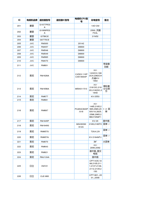
ID 201 202 203 204 205 206 207 208 209 210 211
电视机品牌 遥控器型号 夏普 夏普 夏普 夏普 JVC JVC JVC JVC JVC JVC JVC G1077PES A G1069PES A G756CE G0775CE RM300 RM457 RM548 RM549 RM565 RM470 RM601
USB总线接口芯片CH371中文手册
USB总线接口芯片CH371中文手册(第二版)南京沁恒电子有限公司TEL: 025-*******FAX: 025-*******CH371是一个USB总线的通用接口芯片。
在本地端,CH371具有8位数据总线和读、写、片选控制线以及中断输出,可以方便地挂接到单片机、DSP、MCU等控制器的系统总线上;在计算机系统中,CH371的配套软件提供了简洁易用的操作接口,与本地端的单片机通讯就如同读写硬盘中的文件。
CH371屏蔽了USB通讯中的所有协议,在计算机应用层与本地端控制器之间提供端对端的连接。
基于CH371,不需要了解任何USB协议或者固件程序甚至驱动程序,就可以轻松地将并口、串口的产品升级到USB接口。
2、特点●屏蔽USB协议,在计算机应用层与本地端之间提供端对端的连接。
●两种通讯模式:单向数据流模式、请求加应答模式,支持伪中断。
●自动完成USB配置过程,完全不需要本地端控制器作任何处理。
●标准的USB V1.1接口,即插即用,D+引脚内置上拉电阻。
●内置4个端点,支持USB的控制传输、批量传输、中断传输。
●通用Windows驱动程序,提供设备级接口和应用层接口。
●通用的本地8位数据总线,4线控制:读选通、写选通、片选输入、中断输出。
●占用16个地址,可选直接地址方式或者复用地址方式。
●内置输入输出缓冲区,以中断方式通知本地端控制器传输数据。
●内置硬件实现的I2C主接口,应用层可以直接读写外挂的I2C从设备。
●在主控方式下可以提供16根输入信号线或者12根独立控制的输出信号线。
●内置上电复位,提供高电平有效复位输出和低电平有效复位输出。
●内置可选的看门狗电路Watch-Dog,为本地端控制器提供监控。
●可选多种封装:DIP28、SOP28、DIP24、CHIP。
●底层协议说明以及整体方案请索取相关资料(需签署技术保密协议)。
封装形式宽度引脚间距说明SOP28 7.62mm 300mil 1.27mm 50mil 标准的28脚贴片DIP28 15.24mm 600mil 2.54mm 100mil 标准的28脚双列直插DIP24S 7.62mm 300mil 2.54mm 100mil 标准的窄24脚双列直插4、引脚28脚封装的引脚号24脚封装的引脚号引脚名称类型引脚说明28 24 VCC 电源正电源12 9 GND 电源接地14 11 XI 输入晶体振荡的输入端,带偏置电阻13 10 XO 输出晶体振荡的反相输出端10 7 D+ 双向USB D+数据线,内置上拉电阻可控11 8 D- 双向USB D-数据线9 6 OFF 输入关闭D+上拉电阻,高有效,带下拉22~15 19~12 D7~D0 双向8位双向数据总线,带上拉,直接输入和独立控制输出4 4 RD# 输入读选通输入,低有效,带上拉,同时用于看门狗的清除输入3 3 WR# 输入写选通输入,低有效,带上拉27 23 CS# 输入片选输入,低有效,带下拉2 2 ALE 输入地址锁存使能,高有效,带上拉,下降沿锁存数据总线的复用地址1 1 INT# 输出中断输出,传输成功,低有效5~85部分支持A3~A0 双向4位地址线输入,带上拉,直接输入和独立控制输出24 21 SCL 输出I2C接口的时钟线23 20 SDA 双向I2C接口的数据线,开漏输出带上拉25 22 RST 输出上电复位和看门狗复位,高有效26 不支持RST# 输出上电复位和看门狗复位,低有效5.1. 一般说明本手册中的数据,以B结尾的为二进制数,以H结尾的为十六进制数,否则为十进制数,标注为x的位表示该位可以是任意值。
E71系列 CC1310 超小体积 前向纠错射频芯片的无线串口模块使用教程

产品概述E71系列是基于TI公司CC1310射频芯片的无线串口模块(UART),可工作在431~446.5MHz频段(默认433MHz)、861~876.5MHz频段(默认868MHz)、907~922.5MHz频段(默认915MHz)。
超小体积,仅为同类模块不到1/2的体积,针对体积限制严格的使用场景极为推荐。
模块具有软件FEC前向纠错算法,其编码效率较高,纠错能力强,在突发干扰的情况下,能主动纠正被干扰的数据包,大大提高可靠性和传输距离。
在没有FEC的情况下,这种数据包只能被丢弃。
模块具有数据加密和压缩功能。
模块在空中传输的数据,具有随机性,通过严密的加解密算法,使得数据截获失去意义。
而数据压缩功能有概率减小传输时间,减小受干扰的概率,提高可靠性和传输效率。
E71系列厂无程序均已内置低功耗多功能无线串口程序,用户亦可以根据需要进行二次开发。
目录产品特点 (3)1.技术参数31.1.通用参数31.2.电气参数41.2.1.发射电流41.2.2.接收电流41.2.3.关断电流41.2.4.供电电压41.2.5.通信电平51.3.射频参数51.3.1.发射功率5 1.3.2.接收灵敏度 (5)1.3.3.推荐工作频率 (5)1.4.实测距离62.机械特性62.1.E71-433MS14/E71-868MS14/E71-915MS14 (6)2.2.E71-433MS30/E71-868MS30/E71-915MS30 (8)3.推荐连线图 (10)4.功能详解104.1.定点发射104.2.广播发射114.3.广播地址114.4.监听地址114.5.模块复位114.6.AUX详解11 4.6.1.串口数据输出指示 (11)4.6.2.无线发射指示 (12)4.6.3.模块正在配置过程中 (12)5.工作模式135.1.模式切换135.2.RSSI模式(模式0) (13)5.3.连传模式(模式1) (14)5.4.分包模式(模式2) (14)5.5.配置模式(模式3) (14)5.6.唤醒模式(模式4) (14)5.7.配置模式(模式5) (15)5.8.省电模式(模式6) (15)5.9.休眠模式(模式7) (15)6.指令格式156.1.出厂默认参数 (15)6.2.工作参数读取 (16)6.3.版本号读取166.4.复位指令166.5.参数设置指令 (17)7.参数配置198.二次开发198.1.E71-433MS14/E71-868MS14/E71-915MS14 (19)8.2.E71-433MS30/E71-868MS30/E71-915MS30 (21)8.3.程序烧录 (22)9.生产指导239.1.回流焊温度239.2.回流焊曲线图 (23)10.常见问题2410.1.通信距离很近 (24)10.2.模块易损坏2411.重要声明2412.关于我们24产品特点●【连续传输】:连续传输方式不限数据包的长度,可以完美支持Modbus协议,实现最高115200bps串口波特率的连续不间断传输。
UPD703040中文资料
Document No. U13953EJ1V0DS00 (1st edition) Date Published March 2000 N CP(K)Printed in Japan The mark shows major revised points.©2000Preliminary Data Sheet U13953EJ1V0DS002{ PWM output: 4 channels { Vsync/Hsync separation circuit { On-chip key return function {On-chip clock generator{Power saving function: HALT/IDLE/STOP modes { ROM correction: 4 points changeable { Package: 176-pin plastic LQFP (24 × 24 mm)APPLICATIONS{System/servo/camera control of camcorders {Portable cameras such as digital still cameras{Cellular phones, portable information terminals, etc.ORDERING INFORMATIONPart NumberPackageµPD703039GM-×××-UEU µPD703039YGM-×××-UEU µPD703040GM-×××-UEU µPD703040YGM-×××-UEU µPD703041GM-×××-UEU µPD703041YGM-×××-UEU176-pin plastic LQFP (fine pitch) (24 × 24 mm)176-pin plastic LQFP (fine pitch) (24 × 24 mm)176-pin plastic LQFP (fine pitch) (24 × 24 mm)176-pin plastic LQFP (fine pitch) (24 × 24 mm)176-pin plastic LQFP (fine pitch) (24 × 24 mm)176-pin plastic LQFP (fine pitch) (24 × 24 mm)Remark ××× indicates ROM code suffix.DIFFERENCES BETWEEN V850/SV1 PRODUCTSPIN CONFIGURATION176-pin plastic LQFP (fine pitch) (24 × 24 mm)µPD703039GM-×××-UEUµPD703039YGM-×××-UEUµPD703040GM-×××-UEUµPD703040YGM-×××-UEUµPD703041GM-×××-UEUµPD703041YGM-×××-UEUPreliminary Data Sheet U13953EJ1V0DS003Preliminary Data Sheet U13953EJ1V0DS004PIN IDENTIFICATIONA16 to A21:Address Bus AD0 to AD15:Address/Data Bus ADTRG:AD Trigger Input ANI0 to ANI15:Analog InputASCK0, ASCK1:Asynchronous Serial Clock ASTB:Address Strobe AV DD :Analog Power Supply AV REF :Analog Reference Voltage AV SS :Analog GroundBV DD :Bus Interface Power Supply BV SS :Bus Interface Ground CLKOUT:Clock OutputCLO:Clock Output (divided)CSYNCIN:Csync Input DSTB:Data Strobe HLDAK:Hold Acknowledge HLDRQ:Hold Request HSOUT0, HSOUT1:Hsync OutputIC:Internally ConnectedINTCP80 to INTPC83,:Interrupt Request from PeripheralsINTCP90 to INTCP93,INTP0 to INTP6,INTTCLR8,INTTI8, INTTI9KR0 to KR7:Key Return LBEN:Lower Byte EnableNMI:Non-Maskable Interrupt Request P00 to P07:Port 0P10 to P15:Port 1P20 to P27:Port 2P30 to P37:Port 3P40 to P47:Port 4P50 to P57:Port 5P60 to P65:Port 6P70 to P77:Port 7P80 to P87:Port 8P90 to P96:Port 9P100 to P107:Port 10P110 to P113:Port 11P120 to P127:Port 12P130 to P137:Port 13P140 to P147:Port 14P150 to P157:Port 15P160 to P167:Port 16P170 to P177:Port 17P180 to P187:Port 18P190 to P197:Port 19PWM0 to PWM3:Pulse Width Modulation RD:Read RESET:ResetRTP00 to RTP07,:Real-time Output PortRTP10 to RTP17RTPTRG0, RTPTRG1:RTP Trigger Input R/W:Read/Write Status RXD0, RXD1:Receive Data SCK0 to SCK4:Serial Clock SCL0, SCL1:Serial Clock SDA0, SDA1:Serial Data SI0 to SI4:Serial Input SO0 to SO4:Serial Output TCLR8:Timer Clear TI000, TI001, TI010,:Timer InputTI011, TI2 to TI11TO0 to TO7, TO80,:Timer Output TO81, TO10, TO11TXD0,TXD1:Transmit Data UBEN:Upper Byte Enable V DD :Power Supply VSOUT:Vsync Output V SS :Ground WAIT:WaitWRH:Write Strobe High Level Data Write Strobe Low Level Data X1, X2:Crystal for Main System Clock XT1, XT2:Crystal for Subsystem ClockINTERNAL BLOCK DIAGRAMPreliminary Data Sheet U13953EJ1V0DS005CONTENTS1.PIN FUNCTIONS (7)1.1Port Pins (7)1.2Non-Port Pins (11)1.3Pin I/O Circuits, I/O Buffer Supply, and Recommended Connection of Unused Pins (14)2.ELECTRICAL SPECIFICATIONS (18)3.PACKAGE DRAWING (37)4.RECOMMENDED SOLDERING CONDITIONS (38)6Preliminary Data Sheet U13953EJ1V0DS001.PIN FUNCTIONS1.1Port PinsRemark PULL: on-chip pull-up resistorPreliminary Data Sheet U13953EJ1V0DS007Remark PULL: on-chip pull-up resistor8Preliminary Data Sheet U13953EJ1V0DS00Remark PULL: on-chip pull-up resistorPreliminary Data Sheet U13953EJ1V0DS00910Preliminary Data Sheet U13953EJ1V0DS00(4/4)Pin Name I/O PULL FunctionAlternate Function P150RTP10P151RTP11P152RTP12P153RTP13P154RTP14P155RTP15P156RTP16P157I/ONoPort 158-bit I/O portInput/output mode can be specified in 1-bit units.RTP17P160PWM0P161PWM1P162PWM2P163PWM3P164CSYNCIN P165VSOUT P166HSOUT0P167I/ONoPort 168-bit I/O portInput/output mode can be specified in 1-bit units.HSOUT1P170KR0P171KR1P172KR2P173KR3P174KR4P175KR5P176KR6P177I/OYesPort 178-bit I/O portInput/output mode can be specified in 1-bit units.KR7P180–P181–P182–P183–P184–P185–P186–P187I/ONoPort 188-bit I/O portInput/output mode can be specified in 1-bit units.–P190–P191–P192–P193–P194–P195–P196–P197I/ONoPort 198-bit I/O portInput/output mode can be specified in 1-bit units.–Remark PULL: on-chip pull-up resistor1.2Non-Port PinsRemark PULL: on-chip pull-up resistorRemark PULL: on-chip pull-up resistorRemark PULL: on-chip pull-up resistor1.3Pin I/O Circuits, I/O Buffer Supply, and Recommended Connection of Unused Pins Table 1-1 shows the I/O circuit type of each pin and the recommended connection of unused pins.For the input/output configuration of each type, refer to Figure 1-1.Table 1-1. Types of Pin I/O Circuit and Recommended Connection of Unused Pins (1/2)Table 1-1. Types of Pin I/O Circuit and Recommended Connection of Unused Pins (2/2)Figure 1-1. Pin Input/Output Circuits (1/2)Figure 1-1. Pin Input/Output Circuits (2/2)2.ELECTRICAL SPECIFICATIONSAbsolute Maximum Ratings (T A = 25°C, V SS = 0 V)Parameter Symbol Conditions Ratings Unit Supply voltageV DD–0.5 to +4.6VAV DD–0.5 to +4.6VBV DD–0.5 to +4.6VAV SS–0.5 to +0.5VBV SS–0.5 to +0.5V Input voltageV I1Note 1 (V DD)–0.5 to V DD + 0.5Note 4VV I2Note 2 (BV DD)–0.5 to BV DD + 0.5Note 4V Clock input voltage V K X1, XT1, V DD = 2.7 to 3.6 V–0.5 to V DD + 1.0Note 4Analog input voltage V IAN Note 3 (AV DD)–0.5 to AV DD + 0.5Note 4V Analog reference input voltage AV REF AV REF pin–0.5 to AV DD + 0.5Note 4V Output current, low I OLPer pin 4.0mATotal for P00 to P07, P150 to P15725mATotal for P100 to P107, P160 to P16725mATotal for P170 to P177, P190 to P19725mATotal for P124 to P127, P180 to P18725mATotal for P30 to P37, P120 to P12325mA25mATotal for P12 to P15, P20 to P27, P110 toP113Total for P50 to P57, P60 to P65, CLKOUT25mATotal for P40 to P47, P90 to P9625mATotal for P130 to P137, P140 to P14725mA Output current, high I OHPer pin–4.0mATotal for P00 to P07, P150 to P157–25mATotal for P100 to P107, P160 to P167–25mATotal for P170 to P177, P190 to P197–25mATotal for P124 to P127, P180 to P187–25mATotal for P30 to P37, P120 to P123–25mA–25mATotal for P12 to P15, P20 to P27, P110 toP113Total for P50 to P57, P60 to P65, CLKOUT–25mATotal for P40 to P47, P90 to P96–25mATotal for P130 to P137, P140 to P147–25mA Output voltageV O1Note 1 (V DD)–0.5 to V DD + 0.5VV O2Note 2 (BV DD)–0.5 to BV DD + 0.5V Operating ambient temperature T A–40 to +85°C Storage temperature T stg–65 to +150°C Notes1. Ports 0, 1, 2, 3, 10, 11, 12, 13, 14, 15, 16, 17, 18, 19, RESET (includes alternate function pins)2. Ports 4, 5, 6, 9, CLKOUT, WAIT (includes alternate function pins)3. Ports 7, 8 (includes alternate function pins)4. Be sure not to exceed each absolute maximum rating (MAX.).Cautions1.Do not directly connect to each other output pins (or I/O pins) of IC products, and do not connect them directly to V DD , V CC , or GND. However, open-drain pins and open-connector pins can be directly connected to each other. Moreover, external circuits that implement a timing that avoids conflict with the output of pins that go into high-impedance can be directly connected.2.Product quality may suffer if the absolute maximum rating is exceeded even momentarily for any parameter. That is, the absolute maximum ratings are rated values at which the product is on the verge of suffering physical damage, and therefore the product must be used under conditions that ensure that the absolute maximum ratings are not exceeded.The ratings and conditions indicated for DC characteristics and AC characteristics represent the quality assurance range during normal operation.Capacitance (T A = 25°C, V DD = V SS = 0 V)ParameterSymbol ConditionsMIN.TYP.MAX.Unit Input capacitance C I 15pF I/O capacitance C IO 15pF Output capacitanceC Of C = 1 MHzUnmeasured pins returned to 0 V15pFOperating Conditions(1) CPU Operation FrequencyParameterSymbol ConditionsMIN.TYP.MAX.Unit @ main system clock operation 0.516MHz CPU operation frequencyf CPU@ subsystem clock operation32.768MHz(2) Supply VoltageParameterSymbol ConditionsMIN.TYP.MAX.Unit V DD 2.7 3.6V AV DD 2.7 3.6V Supply voltageBV DD2.73.6V(3) Operation Frequency for Each Supply VoltageInternal Operation Clock FrequencySupply Voltage (V DD = AV DD = BV DD )4 MHz ≤ f XX ≤ 16 MHz 2.7 to 3.6 V f XT = 32.768 kHz2.7 to3.6 VRecommended Oscillator(1)Main System Clock Oscillator (T A = −40 to +85°C)Parameter Symbol Conditions MIN.TYP.MAX.Unit Oscillation frequency f XT3232.76835kHz Oscillation stabilization time10sRemarks 1.Place the oscillator as close as possible to XT1 and XT2.2.Do not wire other signal lines within the broken lines.3.For resonator selection and oscillation constants, customers are advised to either evaluate theoscillation themselves, or apply to the resonator manufacturer for evaluation.DC Characteristics (T A = –40 to +85°C, V DD = AV DD = BV DD = 2.7 to 3.6 V, V SS = AV SS = BV SS = 0 V)Notes1.Ports 4, 5, 6, 9 (includes alternate-function pins)2.P11, P14, P21, P24, P34, P35, P100 to P107, P110 to P113, P121, P123, P136, P137, P146, P147,P150 to P157, P160 to P163, P165 to P167, P180 to P187, P190 to P197 (includes alternate-functionpins)3.P00 to P07, P10, P12, P13, P15, P20, P22, P23, P25 to P27, P30 to P33, P36, P37, P120, P122, P124to P127, P130 to P135, P140 to P145, P164, P170 to P177 (includes alternate-function pins)4.Ports 7, 8 (includes alternate-function pins)5.The typical values listed are those of at V DD = 3.3 V. The current that is consumed at output buffers isnot included.Data Retention Characteristics (T A = –40 to +85°C, V DD = AV DD = BV DD = 2.7 to 3.6 V, V SS = AV SS = BV SS = 0 V)ParameterSymbol ConditionsMIN.TYP.MAX.Unit Data retention voltage V DDDR STOP mode 1.83.6VData retention current I DDDR V DDDR [V]160µA Supply voltage rising time t RVD 200µs Supply voltage falling time t FVD 200µs Supply voltage hold time (from STOP mode setting)t HVD0msSTOP release signal input time t DREL 0ms Data retention high-level input voltage V IHDR All input port V IHn V DDDR V Data retention low-level input voltageV ILDRAll input portV ILnVRemark n = 1 to 5AC CharacteristicsAC Test Input Waveforms (V DD, BV DD, AV DD)Clock TimingOperating Conditions (T A = –40 to +85°C, V DD = AV DD = BV DD = 2.7 to 3.6 V, V SS = AV SS = BV SS = 0 V)ParameterSymbol ConditionMIN.MAX.Unit X1 input cycle 62.5250nsXT1 input cycle t CYX<1>28.631.2µs X1 input high-level width 31.2125nsXT1 input high-level width t WXH<2>14.315.6µs X1 input low-level width 31.2125nsXT1 input low-level width t WXL<3>14.315.6µs X1 input rise time t XR <4>(<1> – <2> – <3>)/2ns X1 input fall time t XF <5>(<1> – <2> – <3>)/2nsCLKOUT output cycle t CYK <6>62.5 ns 31.2 µsCLKOUT high-level width t WKH <7>0.4(T – 20)ns CLKOUT low-level width t WKL <8>0.4(T – 20)ns CLKOUT rise time t KR <9>10ns CLKOUT fall timet KF<10>10nsRemark T = t CYK Clock TimingTiming of Pins Other Than X1 and CLKOUT Pins(T A = –40 to +85°C, V DD = AV DD = BV DD = 2.7 to 3.6 V, V SS = AV SS = BV SS = 0 V, Output Pin Load Capacitance: C L = 50 pF)ParameterSymbol ConditionMIN.MAX.Unit Output rise time t OR 20ns Output fall timet OF20nsBus Timing (CLKOUT Asynchronous)(T A = –40 to +85°C, V DD = AV DD = BV DD = 2.7 to 3.6 V, V SS = AV SS = BV SS = 0 V)Remarks1.T = 1/f CPU (f CPU: CPU operation clock frequency)2.n: Number of wait clocks inserted in the bus cycle.Sampling timing changes when a programmable wait is inserted.3.i: Number of idle states inserted after the read cycle (0 or 1).4.The specifications described above are the values of when a clock of duty ratio 1:1 is input from X1.Bus Timing (CLKOUT Synchronous)(T A = –40 to +85°C, V DD = AV DD = BV DD = 2.7 to 3.6 V, V SS = AV SS = BV SS = 0 V)Remark The specifications described above are the values of when a clock of duty ratio 1:1 is input from X1.Read Cycle (CLKOUT Synchronous/Asynchronous, 1 Wait)Write Cycle (CLKOUT Synchronous/Asynchronous, 1 Wait)Bus HoldReset/Interrupt Timing (T A = –40 to +85°C, V DD = AV DD = BV DD = 2.7 to 3.6 V, V SS = AV SS = BV SS = 0 V)Remarks1.T = 1/f XX2.Tsmp = Noise elimination sampling clock frequencyResetTIn Input Timing (T A = –40 to +85°C, V DD = AV DD = BV DD = 2.7 to 3.6 V, V SS = AV SS = BV SS = 0 V)ParameterSymbol ConditionMIN.MAX.Unit TIn0, TIn1 (n = 00, 01)high-level width 2T sam + 20NotensTIn (n = 2 to 7, 10, 11)high-level width t TIH<58>3/f XX + 20nsTIn0, TIn1 (n = 00, 01)low-level width 2T sam + 20NotensTIn (n = 2 to 7, 10, 11)low-level widtht TIL<59>3/f XX + 20nsNote T sam can be selected by setting the PRMn1 and PRMn0 bits of prescaler mode registers n0, n1 (PRMn0,PRMn1) (n = 0, 1).TM0 (PRM00, PRM01 registers): T sam = 2/f XX , 4/f XX , 16/f XX , 64/f XX , 256/f XX , 1/INTWTI period TM1 (PRM10, PRM11 registers): T sam = 2/f XX , 4/f XX , 16/f XX , 32/f XX , 128/f XX , 256/f XX However, when the TIn0 valid edge is selected as the count clock, T sam = 4/f XX (n = 0, 1).3-Wire SIO Timing(1)Master Mode (T A = –40 to +85°C, V DD = AV DD = BV DD = 2.7 to 3.6 V, V SS = AV SS = BV SS = 0 V)Remark n = 0 to 33-Wire Variable-Length CSI Timing(1)Master Mode (T A = –40 to +85°C, V DD = AV DD = BV DD = 2.7 to 3.6 V, V SS = AV SS = BV SS = 0 V)UART Timing (T A = –40 to +85°C, V DD = AV DD = BV DD = 2.7 to 3.6 V, V SS = AV SS = BV SS = 0 V)ParameterSymbol ConditionMIN.MAX.Unit ASCKn cycle time t KCY13<72>200ns ASCKn high-level width t KH13<73>80ns ASCKn low-level widtht KL13<74>80nsRemark n = 0, 1I 2C Bus Mode (Only for µPD703039Y, 703040Y, and 703041Y)(T A = –40 to +85°C, V DD = AV DD = BV DD = 2.7 to 3.6 V, V SS = AV SS = BV SS = 0 V)Standard Mode High-Speed Mode ParameterSymbolMIN.MAX.MIN.MAX.UnitSCLn clock frequencyf CLK 01000400kHzBus free time(between stop and start conditions)t BUF<75>4.7–1.3–µs Hold timeNote 1t HD : STA <76> 4.0–0.6–µs SCLn clock low-level width t LOW <77> 4.7– 1.3–µs SCLn clock high-level width t HIGH <78> 4.0–0.6–µs Setup time of start/restart conditions t SU : STA<79> 4.7–0.6–µs CBUS-compatible master 5.0–––µs Data hold timeI 2C modet HD : DAT <80>Note 2–0Note 20.9Note 3µs Data setup timet SU : DAT <81>250–100Note 4–ns Rising time of SDAn and SCLn signals t R <82>–100020 + 0.1Cb Note 5300ns Falling time of SDAn and SCLn signals t F <83>–30020 + 0.1CbNote 5300nsSetup time of stop condition t SU : STO <84> 4.0–0.6–µs Pulse width of spike suppressed by input filtert SP<85>––50nsLoad capacitance of bus linesCb –400–400pFNotes 1.The first clock pulse in the start condition is generated after the hold time.2.The system must internally provide at least 300 ns hold time for the SDAn signal (at V IHmin. of the SCLnsignal) in order to fill the undefined area that appears at the SCLn falling edge.3.If the system does not extend the low hold time (t LOW ), it is required to satisfy only the maximum datahold time (t HD : DAT ).4.The high-speed I 2C bus is available in the standard mode I 2C bus system. In this case, followingconditions should be satisfied.•When the system does not extend the low-state hold time of the SCLn signal t SU : DAT ≥ 250 ns•When the system extends the low-state hold time of the SCLn signalBefore the SCLn line is released (t Rmax. + t SU : DAT = 1000 + 250 = 1250 ns: Standard mode I 2C bus specification), send the next data bit to the SDAn line.5.Cb: Total capacitance of one bus line (Unit: pF)Remark n = 0, 1I2C Bus Mode (Only for µPD703039Y, 703040Y, and 703041Y)A/D Converter (T A = –40 to +85°C, V DD = AV DD = AV REF = 2.7 to 3.6 V, AV SS = V SS = 0 V, Output Pin Load Capacitance: C L = 50 pF)Parameter Symbol Conditions MIN.TYP.MAX.Unit Resolution101010bit Overall error Note 1±0.8%FSR Conversion time t CONV5100µs Zero-scale error Note 1±0.4%FSR Full-scale error Note 1±0.4%FSR Integral linearity error Note 2±4.0LSB Differential linearity error Note 2±4.0LSB Analog reference voltage AV REF AV REF = AV DD 2.7 3.6V Analog input voltage V IAN AV SS AV REF V AV REF current AI REF240360µA Supply current AI DD13mA Notes 1. Excluding quantization error (±0.05%FSR)2. Excluding quantization error (±0.5LSB)Remark LSB: Least Significant BitFSR: Full Scale Range3.PACKAGE DRAWING176-PIN PLASTIC LQFP (FINE PITCH) (24x24)NOTEEach lead centerline is located within 0.10 mm ofits true position (T.P.) at maximum material condition.ITEM MILLIMETERS ABDG26.0±0.224.0±0.21.2526.0±0.2S176GM-50-UEU C24.0±0.2L0.5F 1.25NPQS0.081.40.1±0.051.5±0.1M0.17+0.03−0.07H0.22±0.05IJK0.080.5 (T.P.)1.0±0.2R3°+4°−3°4.RECOMMENDED SOLDERING CONDITIONSThe µPD703039, 703039Y, 703040, 703040Y, 703041, and 703041Y should be soldered and mounted under the following recommended conditions.For the details of the recommended soldering conditions, refer to the document Semiconductor Device Mounting Technology Manual (C10535E).For soldering methods and conditions other than those recommended below, contact your NEC sales representative.Table 4-1. Surface Mounting Type Soldering ConditionsµPD703039GM-×××-UEU: 176-pin plastic LQFP (fine pitch) (24 × 24 mm)µPD703040GM-×××-UEU: 176-pin plastic LQFP (fine pitch) (24 × 24 mm)Soldering Method Soldering Conditions RecommendedCondition Symbol Infrared reflow Package peak temperature: 235°C, Time: 30 sec. Max. (at 210°C or higher),IR35-103-2Count: Twice or less, Exposure limit: 3 days Note (after that, prebake at 125°C for 10hours)VPS Package peak temperature: 215°C, Time: 40 sec. Max. (at 200°C or higher),VP15-103-2Count: Twice or less, Exposure limit: 3 days Note (after that, prebake at 125°C for 10hours)Partial heating Pin temperature: 300°C Max., Time 3 sec. Max. (per pin row)Note After opening the dry pack, store it at 25°C or less and 65% RH or less for the allowable storage period.Cautions1. Do not use different soldering methods together (except for partial heating).2. Soldering conditions forµPD703039Y, 703040Y, 703041, and 703041Y are undetermined.[MEMO][MEMO][MEMO]Preliminary Data Sheet U13953EJ1V0DS0041Purchase of NEC I2C components conveys a license under the Philips I2C Patent Rights to use these components in an I2C system, provided that the system conforms to the I2C Standard Specification as defined by Philips.Related documentµPD70F3040, 70F3040Y Data Sheet (U14622E)Reference document Electrical Characteristics for Microcomputer (IEI-601) NoteNote This document number is that of the Japanese version.The documents indicated in this publication may include preliminary versions. However, preliminary versions are not marked as such.V850 Family and V850/SV1 are trademarks of NEC Corporation.42Preliminary Data Sheet U13953EJ1V0DS00Preliminary Data Sheet U13953EJ1V0DS0043Regional InformationSome information contained in this document may vary from country to country. Before using any NEC product in your application, pIease contact the NEC office in your country to obtain a list of authorized representatives and distributors. They will verify:• Device availability• Ordering information• Product release schedule• Availability of related technical literature• Development environment specifications (for example, specifications for third-party tools and components, host computers, power plugs, AC supply voltages, and so forth)• Network requirementsIn addition, trademarks, registered trademarks, export restrictions, and other legal issues may also vary from country to country.NEC Electronics Inc. (U.S.)Santa Clara, CaliforniaTel: 408-588-6000800-366-9782Fax: 408-588-6130800-729-9288NEC Electronics (Germany) GmbH Duesseldorf, Germany Tel: 0211-65 03 02Fax: 0211-65 03 490NEC Electronics (UK) Ltd.Milton Keynes, UKTel: 01908-691-133Fax: 01908-670-290NEC Electronics Italiana ano, ItalyTel: 02-66 75 41Fax: 02-66 75 42 99NEC Electronics (Germany) GmbH Benelux Office Eindhoven, The Netherlands Tel: 040-2445845Fax: 040-2444580NEC Electronics (France) S.A.Velizy-Villacoublay, France Tel: 01-30-67 58 00Fax: 01-30-67 58 99NEC Electronics (France) S.A.Spain Office Madrid, Spain Tel: 91-504-2787Fax: 91-504-2860NEC Electronics (Germany) GmbH Scandinavia Office Taeby, Sweden Tel: 08-63 80 820Fax: 08-63 80 388NEC Electronics Hong Kong Ltd.Hong Kong Tel: 2886-9318Fax: 2886-9022/9044NEC Electronics Hong Kong Ltd.Seoul BranchSeoul, KoreaTel: 02-528-0303Fax: 02-528-4411NEC Electronics Singapore Pte. Ltd.United Square, Singapore 1130Tel: 65-253-8311Fax: 65-250-3583NEC Electronics Taiwan Ltd.Taipei, TaiwanTel: 02-2719-2377Fax: 02-2719-5951NEC do Brasil S.A.Electron Devices DivisionRodovia Presidente Dutra, Km 21407210-902-Guarulhos-SP BrasilTel: 55-11-6465-6810Fax: 55-11-6465-6829J99.1The export of this product from Japan is regulated by the Japanese government. To export this product may be prohibited without governmental license, the need for which must be judged by the customer. The export or re-export of this productfrom a country other than Japan may also be prohibited without a license from that country. Please call an NEC sales representative.• The information contained in this document is being issued in advance of the production cycle for the device. The parameters for the device may change before final production or NEC Corporation, at its own discretion, may withdraw the device prior to its production.• No part of this document may be copied or reproduced in any form or by any means without the prior written consent of NEC Corporation. NEC Corporation assumes no responsibility for any errors which may appear in this document.• NEC Corporation does not assume any liability for infringement of patents, copyrights or other intellectual property rights of third parties by or arising from use of a device described herein or any other liability arising from use of such device. No license, either express, implied or otherwise, is granted under any patents, copyrights or other intellectual property rights of NEC Corporation or others.• Descriptions of circuits, software, and other related information in this document are provided for illustrative purposes in semiconductor product operation and application examples. The incorporation of these circuits, software, and information in the design of the customer's equipment shall be done under the full responsibility of the customer. NEC Corporation assumes no responsibility for any losses incurred by the customer or third parties arising from the use of these circuits, software, and information.• While NEC Corporation has been making continuous effort to enhance the reliability of its semiconductor devices, the possibility of defects cannot be eliminated entirely. To minimize risks of damage or injury to persons or property arising from a defect in an NEC semiconductor device, customers must incorporate sufficient safety measures in its design, such as redundancy, fire-containment, and anti-failure features.• NEC devices are classified into the following three quality grades:"Standard", "Special", and "Specific". The Specific quality grade applies only to devices developed based on a customer designated "quality assurance program" for a specific application. The recommended applications ofa device depend on its quality grade, as indicated below. Customers must check the quality grade of each devicebefore using it in a particular application.Standard: Computers, office equipment, communications equipment, test and measurement equipment, audio and visual equipment, home electronic appliances, machine tools, personal electronic equipment and industrial robotsSpecial: Transportation equipment (automobiles, trains, ships, etc.), traffic control systems, anti-disaster systems, anti-crime systems, safety equipment and medical equipment (not specifically designed for life support)Specific: Aircraft, aerospace equipment, submersible repeaters, nuclear reactor control systems, life support systems or medical equipment for life support, etc.The quality grade of NEC devices is "Standard" unless otherwise specified in NEC's Data Sheets or Data Books.If customers intend to use NEC devices for applications other than those specified for Standard quality grade, they should contact an NEC sales representative in advance.M5 98. 8。
长虹电视资料
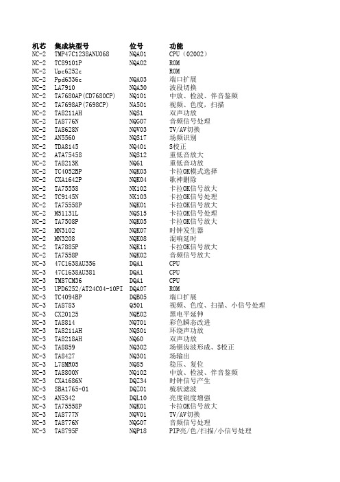
位号 NQA01 NQAO2
NQA03 NQA30 NQ101 NA501 NQS1 NQG07 NQV03 NQS17 NQ401 NQS12 NQ61 NQK03 NQK04 NK102 NK103 NQKO1 NQS15 NQK05 NQK07 NQK08 NQK11 NQK02 DQA1 DQA1 DQA1 DQA07 DQB05 Q501 NQE02 NQT01 NQS01 NQ60 NQ302 NQ301 NQ85 NQ102 DQZ34 DQZ01 DQL10 NQK01 NQV01 NQG07 NQP18
LC7480 LC7441 MBB1461-12PS LC7444 AN5612 AN5862 TC74HC4066F UPD6325C TC9415N TC4052BP CXA1642P TA7558P M51131L TA7508P MN3102 MN3208 M5218AP MSP3410 TMP87C38N NM24C08EN TA1222 TA8256HY STR-6709 HIC1015 TA8859 TA8427 TC9090N MN1031X5 TA1229N TA8772AN TDA9808 JLC15928F NJM2234 MSP3410B-F7 UPC1830GT TA8765N TC9083F PC1406HA TA75458P TA1218N CXA1642P TC4052BP LM358 TA1216AN ATQ203 M6583SP TDA4605-3
集成块型号 TMP47C1238ANU068 TC89101P Upc6252c Ppd6336c LA7910 TA7680AP(CD7680CP) TA7698AP(7698CP) TA8211AH TA8776N TA8628N AN5560 TDA8145 ATA75458 TA8213K TC4052BP CXA1642P TA75558 TC9145N TA75558P M51131L TA7508P MN3102 MN3208 TA7885P TA7558P 47C1638AU356 47C1638AU381 TM87CM36 UPD6252/AT24C04-10PI TC4094BP TA8783 CX20125 TA8814 TA8211AH TA8218AH TA8859 TA8427 L78MR05 TA8800N CXA1686N SBA1765-01 AN5342 TA75558P TA8777N TA8776N TA8795F
u开头的集成电路

UPD6453-554 字符发生集成电路
UPD6453CY564 字符发生集成电路
UPD6461 字符发生集成电路
UPD6901 数/模转换集成电路
UPD70014 微处理集成电路
UPD75106-741-3BE 微处理集成电路
UPD75116GF-F70-3BE 微处理集成电路
UPC1212C 音频功率放大1W集成电路
UPC1222C 调频/调幅中频放大集成电路
UPC1230H2 音频功率放大20W集成电路
UPC1238H 音频功率放大集成电路
UPC1260 双声道功率放大集成电路
UPC1274V 双声道音频功率放大集成电路
UPC1275G 双声道杜比降噪集成电路
UPC1365C 亮度、色度信号处理集成电路
UPC1365C3 色度、亮度信号处理集成电路
UPC1366C 图像中频放大集成电路
UPC1377C 同步信号处理集成电路
UPC1378H 场扫描信号处理集成电路
UPC1378H-L 场扫描信号处理集成电路
UPC1382C 伴音中频放大、鉴频及前置放大集成电路
UPD1943C 红外遥控信号发射集成电路
UPD1986C 红外遥控信号发射集成电路
UPD4011BG 与门集成电路
UPD41464C 存储集成电路
UPD42272A 画中画信号处理集成电路
UPD42280V-30 存储集成电路
UPD424260 动态存储4MB集成电路
UPD424800LE 存储集成电路
UPD6102G 红外遥控信号发射集成电路
MD2203中文资料
Data Sheet
January 2002
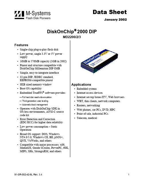
DiskOnChip 2000 DIP
MD2200/2/3 Features
Single-chip plug-n-play flash disk Low power, single 3.3V or 5V power
6 7
Theory of Operation................................................................................................................. 12 6.1 Error Detection and Correction (EDC/ECC) ....................................................................... 12 Specifications .......................................................................................................................... 13 7.1 Absolute Maximum Ratings................................................................................................ 13 7.2 Capacitance ....................................................................................................................... 13 7.3 Temperature Ranges ......................................................................................................... 13 7.4 DiskOnChip Assembly........................................................................................................ 13 7.5 Humidity ............................................................................................................................. 13 7.6 EDC/ECC ........................................................................................................................... 13 7.7 DC Electrical Characteristics over Operating Range.......................................................... 14
磐启微电子 PAN3020 产品说明书

PAN3020产品说明书低成本高性能Sub-1G无线收发芯片概述PAN3020是一款工作在1GHz以下的多个频段,如315MHz / 433MHz / 868MHz / 915MHz(后称为315频段、433频段、868频段和915频段)等通用ISM频段,的单片无线收发芯片。
该芯片集成射频收发器、频率综合器、晶体振荡器、调制解调器等功能模块,并且支持一对多组网和带ACK的通信模式。
发射输出功率、工作频道以及通信数据率均可配置。
主要特性1.支持1GHz以下的多个频段。
2.支持40Kbps、80Kbps、200Kbps和400Kbps四种通信数据率。
3.最大发射输出功率20dBm;433频段的40Kbps的接收灵敏度-112dBm。
其它特性支持FEC功能 支持连续发射模式SPI 接口速率最高支持8Mbps GFSK通信方式支持最大数据长度为32/64字节 SOP16封装支持16MHz晶振±10ppm 工作电压支持2.2~3.3V数据扰码 数据自动校验自带温度检测功能 支持自动应答及自动重传应用方案遥控器 智能家居工业控制安防系统无线语音MISOMOSICSNSCKIRQCEVSSVDDVDVDDVSS版本 修订时间 更新内容 相关文档V1.5 2016. 06 新增QFN20封装形式 《02_PAN3020硬件设计和调试参考》《03_PAN3020软件设计和调试参考》《04_PAN3020_RFdemo》 《05_PAN3020_SampleCode》 《06_PN3020 各频段软件配置和硬件匹配区别说明》目录1 命名规则 (4)1.1 PAN3020命名规则 (4)1.2 PAN3020系列产品选择 (4)2 电气特性 (4)2.1主要电特性 (4)2.2 极限最大额定值 (4)3 引脚定义 (6)4 工作模式 (8)4.1 工作模式切换 (8)4.2 休眠模式 (9)4.3 待机模式-I (9)4.4 待机模式-II (9)4.5 接收模式 (10)4.6 发射模式 (10)4.7 连续发射模式 (10)5 数据包格式 (11)5.1 DATA FIFO结构 (11)5.2普通模式的数据包形式 (11)5.3 增强模式的数据包形式 (12)5.4 增强模式的ACK包形式 (12)6 通信模式 (13)6.1 普通模式 (14)6.2 增强模式 (14)6.3增强发送模式 (15)6.4 增强接收模式 (17)6.5 增强模式下的数据包识别 (18)6.6 增强模式下的PTX和PRX的时序图 (18)6.7 增强模式下的接收端一对多通信 (19)6.8 中断引脚 (21)7 SPI控制接口 (22)7.1 SPI接口 (22)7.2 SPI 时序 (22)7.3 4线SPI读操作 (23)7.4 4线SPI写操作 (23)7.5 SPI指令格式 (24)8 控制寄存器 (26)9 射频参数设定 (46)9.1 频率设定 (46)9.2 功率设定 (46)9.3 内部时钟输出设定 (46)9.4 晶振的芯片内部电容设定 (46)10 典型应用电路 (48)11 封装尺寸 (50)12 联系方式 (52)1 命名规则1.1 PAN3020命名规则图2 PAN3020系列芯片命名规则1.2 PAN3020系列产品选择表1.1 PAN3020系列产品选择产品型号芯片版本封装形式PAN3020BV B VPAN3020BL B L2 电气特性2.1主要电特性表2.1 主要电特性特 性 条件(除另有规定外,VCC = 3V±5%, TA=25℃)参数值 单位 最小 典型 最大ICC休眠模式 2 uA待机模式I 50 uA待机模式Ⅱ 750 uA 发射模式 (1dBm) 20 mA发射模式 (8dBm) 30 mA发射模式 (15dBm) 50 mA发射模式 (20dBm) 85 mA 接收模式 (DR=400Kbps) 18 18.5 mA接收模式 (DR=200Kbps) 18 18.5 mA 接收模式(DR=80Kbps) 18 18.5 mA 接收模式(DR=40Kbps)1818.5mA系统指标OP f工作频率(315频段) 270 360 MHz 工作频率(433频段) 400 550 MHz 工作频率(868/915频段)800 1100 MHz res PLL锁相环频率步径20 KHz XTAL f晶振频率 16 MHz DR码率40 Kbps 80 Kbps 200 Kbps400 Kbps f调制频偏@40Kbps 20 KHz 调制频偏@80Kbps 40 KHz 调制频偏@200Kbps 100 KHz 调制频偏@400Kbps200 KHz FCH频道间隔@40Kbps 120 KHz 频道间隔@80Kbps 240 KHz 频道间隔@200Kbps 600 KHz 频道间隔@400Kbps1200 KHz 发射模式指标PRF 典型输出功率15 dBm PRFC 输出功率范围(315/433频段) -70 20 dBm 输出功率范围(868/915频段) -70 15 dBm PBW载波调制的20dB 带宽(40Kbps) 80 KHz 载波调制的20dB 带宽(80Kbps) 160 KHz 载波调制的20dB 带宽(200Kbps) 400 KHz 载波调制的20dB 带宽(400Kbps)800 KHz 接收模式指标max RX误码率<0.1%时的最大接收幅度 0 dBm RXSENS接收灵敏度(0.1%BER,DR=40Kbps,△f=±20KHz,@433频段)-112dBm接收灵敏度(0.1%BER,DR=80Kbps,△f=±40KHz,-109 dBm@433频段)-106 dBm 接收灵敏度(0.1%BER,DR=200Kbps,△f=±100KHz,@433频段)-103 dBm 接收灵敏度(0.1%BER,DR=400Kbps,△f=±200KHz,@433频段)-112 dBm 接收灵敏度(0.1%BER,DR=40Kbps,△f=±20KHz,@315频段)-109 dBm 接收灵敏度(0.1%BER,DR=80Kbps,△f=±40KHz,@315频段)-106 dBm 接收灵敏度(0.1%BER,DR=200Kbps,△f=±100KHz,@315频段)-103 dBm 接收灵敏度(0.1%BER,DR=400Kbps,△f=±200KHz,@315频段)接收灵敏度(0.1%BER,-107 dBm DR=40Kbps,△f=±20KHz,@868频段)-104 dBm 接收灵敏度(0.1%BER,DR=80Kbps,△f=±40KHz,@868频段)-101 dBm 接收灵敏度(0.1%BER,DR=200Kbps,△f=±100KHz,@868频段)-98 dBm 接收灵敏度(0.1%BER,DR=400Kbps,△f=±200KHz,@868频段)-107 dBm 接收灵敏度(0.1%BER,DR=40Kbps,△f=±20KHz,@915频段)-104 dBm 接收灵敏度(0.1%BER,DR=80Kbps,△f=±40KHz,@915频段)接收灵敏度(0.1%BER,DR=200Kbps,△f=±100KHz,@915频段) -101 dBm接收灵敏度(0.1%BER,DR=400Kbps,△f=±200KHz,@915频段)-98 dBmCO C I /同频的通道选择性@40Kbps 13 dBc ST C 1/I第1相邻道选择性@40Kbps -21 dBc ND C 2/I 第2相邻道选择性@40Kbps -35 dBc RD C 3/I 第3相邻道选择性@40Kbps -43 dBc CO C I /同频的通道选择性@80Kbps 13 dBc ST C 1/I 第1相邻道选择性@80Kbps -20 dBc ND C 2/I 第2相邻道选择性@80Kbps -33 dBc RD C 3/I第3相邻道选择性@80Kbps -42 dBc BLOCK偏离1MHz 阻塞@40Kbps -53 dBc 偏离4MHz 阻塞@40Kbps -57 dBc 偏离8MHz 阻塞@40Kbps-65 dBc IR镜像抑制-30 dBc 操作条件VDD 供电电压 2.2 3 3.3 V VSS 芯片地 0 V OHV高电平输出电压 VDD-0.3 VDD V OL V低电平输出电压 VSS VSS+0.3 V IH V 高电平输入电压 VDD-0.3 VDD V IL V 低电平输入电压VSSVSS+0.3V2.2 极限最大额定值表2.2 PAN3020极限最大额定值特 性 条件参数值 单位最小典型 最大 最大额定值DD V 供电电压 -0.3 3.6 V I V 输入电压 -0.3 5 V O V输出电压VSS VDD Pd总功耗(TA=-40℃~85℃)400mWOP T工作温度 -40 125 ℃ STG T存储温度-40140℃* 注意:使用中强行超过一项或多项极限最大额定值会导致器件永久性损坏。
uPD77110GC-9EU资料
3
µPD77110, 77111, 77112
PIN CONFIGURATION
+2.5 V +3 V
Serial interface #1
SO1 SORQ1 SOEN1 SCK1 SI1 SIEN1 SIAK1 SO2 SOEN2 SCK2 SI2 SIEN2 (4) P0 - P3
IVDD
EVDD
µPD77110 : 15.3 ns MIN (65 MHz MAX)
13.3 ns MIN (75 MHz MAX) (Operating voltage and ambient temperature are limited.)
µPD77111 : 13.3 ns MIN (75 MHz MAX) µPD77112 : 13.3 ns MIN (75 MHz MAX)
32K × 16 each
None
16K × 16 each
None
8K × 16 each
Data Sheet U12801EJ5V0DS00
30 ns (33 MHz) –
16.6 ns (60 MHz) ×1, 2, 3, 4, 8 (mask option) Fixed to ×4
15.3 ns (65 MHz) Integer of ×1 to 8 (external pin)
z Memory • Internal instruction memory
µPD77110 : RAM 35.5K words × 32 bits µPD77111 : RAM 1K words × 32 bits
Mask ROM 31.75K words × 32 bits
µPD77112 : RAM 1K words × 32 bits