AO4456中文资料
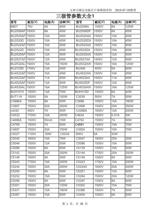
常用三极管参数大全
玉林万顺达电脑芯片级维修资料 2010-07-20整理玉林万顺达电脑芯片级维修资料 2010-07-20整理玉林万顺达电脑芯片级维修资料 2010-07-20整理玉林万顺达电脑芯片级维修资料 2010-07-20整理玉林万顺达电脑芯片级维修资料 2010-07-20整理玉林万顺达电脑芯片级维修资料 2010-07-20整理玉林万顺达电脑芯片级维修资料 2010-07-20整理玉林万顺达电脑芯片级维修资料 2010-07-20整理玉林万顺达电脑芯片级维修资料 2010-07-20整理玉林万顺达电脑芯片级维修资料 2010-07-20整理玉林万顺达电脑芯片级维修资料 2010-07-20整理玉林万顺达电脑芯片级维修资料 2010-07-20整理玉林万顺达电脑芯片级维修资料 2010-07-20整理玉林万顺达电脑芯片级维修资料 2010-07-20整理玉林万顺达电脑芯片级维修资料 2010-07-20整理玉林万顺达电脑芯片级维修资料 2010-07-20整理玉林万顺达电脑芯片级维修资料 2010-07-20整理玉林万顺达电脑芯片级维修资料 2010-07-20整理玉林万顺达电脑芯片级维修资料 2010-07-20整理玉林万顺达电脑芯片级维修资料 2010-07-20整理玉林万顺达电脑芯片级维修资料 2010-07-20整理玉林万顺达电脑芯片级维修资料 2010-07-20整理玉林万顺达电脑芯片级维修资料 2010-07-20整理玉林万顺达电脑芯片级维修资料 2010-07-20整理玉林万顺达电脑芯片级维修资料 2010-07-20整理玉林万顺达电脑芯片级维修资料 2010-07-20整理玉林万顺达电脑芯片级维修资料 2010-07-20整理玉林万顺达电脑芯片级维修资料 2010-07-20整理玉林万顺达电脑芯片级维修资料 2010-07-20整理玉林万顺达电脑芯片级维修资料 2010-07-20整理。
ACPL-W456-000E中文资料

200 TEMPERATURE (°C)
160°C 150°C 140°C
PEAK TEMP. 230°C
2.5°C ± 0.5°C/SEC. 30 SEC. 3°C + 1°C/-0.5°C 30 SEC.
SOLDERING TIME 200°C
100
PREHEATING TIME 150°C, 90 + 30 SEC. 50 SEC. TIGHT TYPICAL LOOSE
ROOM TEMPERATURE
0
0
50
100 TIME (SECONDS)
150
200
250
Note: Non-halide flux should be used.
元器件交易网
Recommended Pb-Free IR Profile
tp Tp TEMPERATURE (˚C) TL T smax T smin ts PREHEAT 60 to 180 SEC. 25 t 25°C to PEAK � TIME (SECONDS) NOTES: THE TIME FROM 25 °C to PEAK TEMPERATURE = 8 MINUTES MAX. Tsmax = 200°C, Tsmin = 150°C Note: Non-halide flux should be used. tL 60 to 150 SEC. 260 +0/-5°C 217°C RAMP-UP 3°C/SEC. MAX. � 150 - 200 °C RAMP-DOWN 6°C/SEC. MAX. TIME WITHIN 5°C of ACTUAL PEAK TEMPERATURE 20-40 SEC.
AO4409中文资料
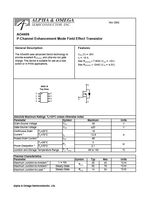
SymbolTyp Max 26405075R θJL 1424Maximum Junction-to-Lead CSteady-State°C/WThermal Characteristics ParameterUnits Maximum Junction-to-Ambient A t ≤ 10s R θJA °C/W Maximum Junction-to-Ambient A Steady-State °C/W AO4409SymbolMin TypMaxUnits BV DSS -30V -5T J =55°C-25I GSS ±100nA V GS(th)-1.4-1.9-2.7V I D(ON)80A 6.27.5T J =125°C8.211.59.512m Ωg FS 3550S V SD -0.71-1V I S-5A C iss 5270pF C oss 945pF C rss 745pF R g 2ΩQ g 100nC Q g (4.5V)51.5nC Q gs 14.5nC Q gd 23nC t D(on)14ns t r 16.5ns t D(off)76.5ns t f 37.5ns t rr 36.7ns Q rr 28nCBody Diode Reverse Recovery Time Body Diode Reverse Recovery ChargeI F =-15A, dI/dt=100A/µsDrain-Source Breakdown Voltage On state drain currentI D =-250µA, V GS =0V V GS =-10V, V DS =-5V V GS =-10V, I D =-15AReverse Transfer Capacitance I F =-15A, dI/dt=100A/µs Electrical Characteristics (T J =25°C unless otherwise noted)STATIC PARAMETERS ParameterConditions I DSS µA Gate Threshold Voltage V DS =V GS I D =-250µA V DS =-24V, V GS =0VV DS =0V, V GS =±20V Zero Gate Voltage Drain Current Gate-Body leakage current R DS(ON)Static Drain-Source On-ResistanceForward Transconductance Diode Forward Voltage m ΩV GS =-4.5V, I D =-10AI S =-1A,V GS =0V V DS =-5V, I D =-15A Turn-On Rise Time Turn-Off DelayTime V GS =-10V, V DS =-15V, R L =1Ω, R GEN =3ΩGate resistance V GS =0V, V DS =0V, f=1MHzTurn-Off Fall Time SWITCHING PARAMETERS Total Gate Charge V GS =-10V, V DS =-15V, I D =-15AGate Source Charge Maximum Body-Diode Continuous CurrentInput Capacitance Output Capacitance Turn-On DelayTime DYNAMIC PARAMETERS V GS =0V, V DS =-15V, f=1MHz Gate Drain Charge Gate Charge A: The value of R θJA is measured with the device mounted on 1in 2FR-4 board with 2oz. Copper, in a still air environment with T A =25°C. The value in any a given application depends on the user's specific board design. The current rating is based on the t ≤ 10s thermal resistance rating.B: Repetitive rating, pulse width limited by junction temperature.C. The R θJA is the sum of the thermal impedence from junction to lead R θJL and lead to ambient.D. The static characteristics in Figures 1 to 6,12,14 are obtained using 80 µs pulses, duty cycle 0.5% max.E. These tests are performed with the device mounted on 1 in 2FR-4 board with 2oz. Copper, in a still air environment with T A =25°C. The SOA curve provides a single pulse rating.。
AO4485中文资料
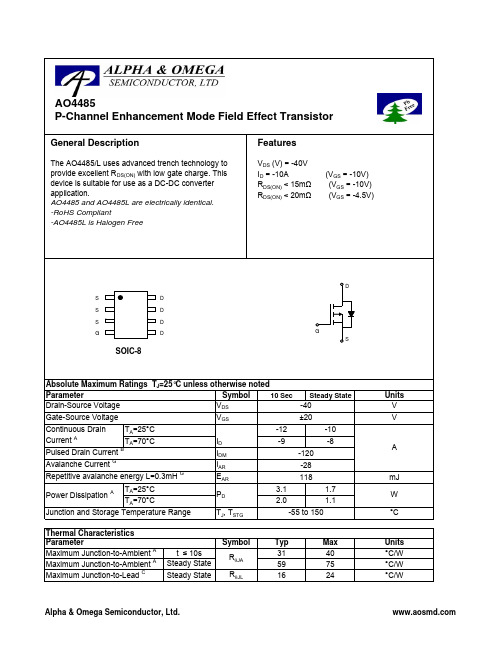
ParameterSymbolTyp Max t ≤ 10s 3140Steady State 5975Steady StateR θJL 1624°C/W R θJA Maximum Junction-to-Lead C°C/WThermal Characteristics Units Maximum Junction-to-Ambient A °C/W Maximum Junction-to-Ambient A AO4485P-Channel Enhancement Mode Field Effect TransistorSymbolMin TypMaxUnits BV DSS -40V -1T J = 55°C-5I GSS ±100nA V GS(th)-1.7-1.9-2.5V I D(ON)-120A12.515T J =125°C19231620g FS 25S V SD -0.7-1V I S-3A C iss 25003000pF C oss 260pF C rss 180pF R g2.546ΩQ g (10V)4255nC Q g (4.5V)18.6nC Q gs 7nC Q gd 8.6nC t D(on)9.4ns t r 20ns t D(off)55ns t f 30ns t rr 3849ns Q rr47nC 0THIS PRODUCT HAS BEEN DESIGNED AND QUALIFIED FOR THE CONSUMER MARKET. APPLICATIONS OR USES AS CRITICAL COMPONENTS IN LIFE SUPPORT DEVICES OR SYSTEMS ARE NOT AUTHORIZED. AOS DOES NOT ASSUME ANY LIABILITY ARISING OUT OF SUCH APPLICATIONS OR USES OF ITS PRODUCTS. AOS RESERVES THE RIGHT TO IMPROVE PRODUCT DESIGN,FUNCTIONS AND RELIABILITY WITHOUT NOTICE.SWITCHING PARAMETERS DYNAMIC PARAMETERS Maximum Body-Diode Continuous CurrentTotal Gate Charge V GS =0V, V DS =0V, f=1MHzV GS =0V, V DS =-20V, f=1MHz Input Capacitance Gate Source Charge Gate Drain Charge µA Total Gate Charge V GS =-10V, V DS =-20V, I D =-10AOutput Capacitance I S = -1A,V GS = 0V V DS = -5V, I D = -10AForward TransconductanceGate resistanceTurn-Off DelayTime V GS =-10V, V DS =-20V, R L = 2Ω, R GEN =3ΩTurn-Off Fall TimeTurn-On DelayTime Turn-On Rise Time m ΩGate Threshold Voltage V DS = V GS I D = -250µA Electrical Characteristics (T J =25°C unless otherwise noted)STATIC PARAMETERS ParameterConditionsI DSS R DS(ON)Drain-Source Breakdown Voltage Body Diode Reverse Recovery TimeBody Diode Reverse Recovery Charge I F =-10A, dI/dt=100A/µsV GS = -10V, I D = -10AReverse Transfer Capacitance I F =-10A, dI/dt=100A/µsStatic Drain-Source On-ResistanceDiode Forward Voltage V GS = -4.5V, I D = -8AOn state drain currentI D = -250µA, V GS = 0V V GS = -10V, V DS = -5V V DS = -40V, V GS = 0VV DS = 0V, V GS = ±20V Zero Gate Voltage Drain Current Gate-Body leakage current A: The value of R θJA is measured with the device mounted on 1in 2 FR-4 board with 2oz. Copper, in a still air environment with T A = 25°C. The value in any given application depends on the user's specific board design.B: Repetitive rating, pulse width limited by junction temperature.C. The R θJA is the sum of the thermal impedence from junction to lead R θJL and lead to ambient.D. The static characteristics in Figures 1 to 6 are obtained using t ≤ 300µs pulses, duty cycle 0.5% max.E. These tests are performed with the device mounted on 1 in 2 FR-4 board with 2oz. Copper, in a still air environment with T A =25°C. The SOA curve provides a single pulse rating.F. The current rating is based on the t ≤ 10s thermal resistance rating.G. E AR and I AR ratings are based on low frequency and duty cycles to keep T j =25C.Rev0 April 2008。
MAX4466EXK中文资料

5-Pin SC70 (derate 2.5mW/°C above +70°C) .............200mW 5-Pin SOT23 (derate 7.1mW/°C above +70°C) ...........571mW
ELECTRICAL CHARACTERISTICS
(VCC = +5V, VCM = 0, VOUT = VCC/2, RL = ∞ to VCC/2, SHDN = GND (MAX4467/MAX4468 only). TA = TMIN to TMAX, unless otherwise noted. Typical values specified at TA = +25°C.) (Note 1)
TOP VIEW
IN+ 1
5 VCC
MAX4465 GND 2 MAX4466
IN- 3
4 OUT
SC70/SOT23 Pin Configurations continued at end of data sheet.
Rail-to-Rail is a registered trademark of Nippon Motorola, Ltd.
Features
o +2.4V to +5.5V Supply Voltage Operation
o Versions with 5nA Complete Shutdown Available (MAX4467/MAX4468)
CDRH64NP-1OOMB中文资料

仕 様 書形 名CDRH641.外形1-1.寸法図(mm)1-2.捺印表示例 1-3.推奨ランド寸法 (mm)2.コイル仕様 2-1.端子接続図(裏面図)電極(端子)間の隙間はシルク処理をして御使用下さい。
頭部直捺印捺印位置不定compliance Cd:Max.0.01wt%others:Max.0.1wt%RoHS1仕 様 書 形 名CDRH642-2.電気的特性Ⅰ(リール の場合)NO. 品 名 表示 インダクタンス[以内]※1D.C.R.(Ω)[以下](at 20℃)※2定格電流(A)※3スミダコード0102 CDRH64NP-1ØØMCCDRH64NP-12ØMC10012010 μH ± 20%12 μH ± 20%0.11(84m)0.13(96m)1.681.514732-00134732-00150304 CDRH64NP-15ØMCCDRH64NP-18ØMC15018015 μH ± 20%18 μH ± 20%0.14(0.11)0.16(0.12)1.321.184732-00164732-00170506 CDRH64NP-22ØMCCDRH64NP-27ØMC22027022 μH ± 20%27 μH ± 20%0.21(0.16)0.29(0.23)1.060.954732-00184732-00190708 CDRH64NP-33ØMCCDRH64NP-39ØMC33039033 μH ± 20%39 μH ± 20%0.33(0.25)0.35(0.27)0.880.774732-00204732-00210910 CDRH64NP-47ØMCCDRH64NP-56ØMC47056047 μH ± 20%56 μH ± 20%0.39(0.30)0.43(0.34)0.760.674732-00224732-00231112 CDRH64NP-68ØMCCDRH64NP-82ØMC68082068 μH ± 20%82 μH ± 20%0.59(0.46)0.66(0.51)0.600.574732-00244732-00261314 CDRH64NP-1Ø1MCCDRH64NP-121MC101121100μH ± 20%120μH ± 20%0.76(0.58)0.83(0.64)0.500.474732-00274732-00281516 CDRH64NP-151MCCDRH64NP-181MC151181150μH ± 20%180μH ± 20%1.24(0.96)1.89(1.51)0.420.374732-00294732-00301718 CDRH64NP-221MCCDRH64NP-271MC221271220μH ± 20%270μH ± 20%2.10(1.68)2.37(1.90)0.340.314732-00314732-00321920 CDRH64NP-331MCCDRH64NP-391MC331391330μH ± 20%390μH ± 20%2.66(2.13)2.94(2.35)0.270.264732-00334732-00342122 CDRH64NP-471MCCDRH64NP-561MC471561470μH ± 20%560μH ± 20%3.89(3.11)5.25(4.20)0.240.214732-00354732-00372324 CDRH64NP-681MCCDRH64NP-821MC681821680μH ± 20%820μH ± 20%5.97(4.78)6.54(5.23)0.180.174732-00384732-003925 CDRH64NP-1Ø2MC 102 1.0 mH ± 20% 8.94(7.15) 0.16 4732-0040※1: 測定周波数 L at 1 kHz※2: ( )内は、標準値とする。
AO4924中文资料
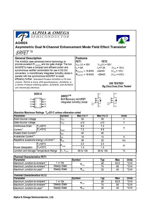
AO4924Asymmetric Dual N-Channel Enhancement Mode Field Effect TransistorAO4924SymbolMin TypMaxUnits BV DSS 30V V DS =24V, V GS =0V0.010.1T J =125°C510I GSS 0.1µA V GS(th)Gate Threshold Voltage 1.5 1.852.4V I D(ON)40A 1315.8T J =125°C20.025.015.719.5m Ωg FS 64S V SD 0.40.6V I S4.5A C iss 14501885pF C oss 224pF C rss92pF R g 1.6 3 ΩQ g (10V)24.031Q g (4.5V)12.0nC Q gs 3.9nC Q gd 4.2nC t D(on) 5.5ns t r 4.7ns t D(off)24.0ns t f 4.0ns t rr 1013ns Q rr6.8nCTHIS PRODUCT HAS BEEN DESIGNED AND QUALIFIED FOR THE CONSUMER MARKET. APPLICATIONS OR USES AS CRITICAL COMPONENTS IN LIFE SUPPORT DEVICES OR SYSTEMS ARE NOT AUTHORIZED. AOS DOES NOT ASSUME ANY LIABILITY ARISING OUT OF SUCH APPLICATIONS OR USES OF ITS PRODUCTS. AOS RESERVES THE RIGHT TO IMPROVE PRODUCT DESIGN,FUNCTIONS AND RELIABILITY WITHOUT NOTICE.Body Diode Reverse Recovery Time Body Diode Reverse Recovery ChargeI F =9A, dI/dt=300A/µsDrain-Source Breakdown Voltage On state drain currentI D =1mA, V GS =0V V GS =4.5V, V DS =5V V GS =10V, I D =9AReverse Transfer CapacitanceI F =9A, dI/dt=300A/µs V DS =V GS I D =250µA FET1 Electrical Characteristics (T J =25°C unless otherwise noted)STATIC PARAMETERS Parameter Conditions I DSS Zero Gate Voltage Drain Current mA V DS =0V, V GS = ±12V Gate-Body leakage current R DS(ON)Static Drain-Source On-ResistanceForward TransconductanceDiode Forward VoltageMaximum Body-Diode + Schottky Continuous CurrentInput Capacitance Output Capacitance DYNAMIC PARAMETERS m ΩV GS =4.5V, I D =7AI S =1A,V GS =0V V DS =5V, I D =9ATurn-On Rise Time Turn-Off DelayTime V GS =10V, V DS =15V, R L =1.7Ω, R GEN =3ΩTurn-Off Fall TimeTurn-On DelayTime Total Gate Charge V GS =10V, V DS =15V, I D =9AGate Drain Charge V GS =0V, V DS =15V, f=1MHzSWITCHING PARAMETERS Total Gate Charge Gate Source Charge Gate resistance V GS =0V, V DS =0V, f=1MHz A: The value of R θJA is measured with the device in a still air environment with T A =25°C. The power dissipation P DSM and current rating I DSM are based on T (J(MAX)=150°C, using t ≤ 10s junction-to-ambient thermal resistance.B: Repetitive rating, pulse width limited by junction temperature T J(MAX)=150°C.C. The R θJA is the sum of the thermal impedence from junction to lead R θJL and lead to ambient.D. The static characteristics in Figures 1 to 6 are obtained using <300 µs pulses, duty cycle 0.5% max.E. These tests are performed with the device mounted on 1 in 2 FR-4 board with 2oz. Copper, in a still air environment with T A =25°C. The SOA curve provides a single pulse rating. Rev0:Sept. 2006AO4924AO4924AO4924AO4924SymbolMin TypMaxUnits BV DSS 30V 1T J =55°C5I GSS 100nA V GS(th)0.711.5V I D(ON)40A 2024T J =125°C283423.529m Ωg FS 26S V SD 0.711V I S4.5A C iss 9001100pF C oss 88pF C rss 65pF R g0.95 1.5ΩQ g 1012nC Q gs 1.8nC Q gd 3.75nC t D(on) 3.2ns t r 3.5ns t D(off)21.5ns t f 2.7ns t rr 16.820ns Q rr812nCTHIS PRODUCT HAS BEEN DESIGNED AND QUALIFIED FOR THE CONSUMER MARKET. APPLICATIONS OR USES AS CRITICAL COMPONENTS IN LIFE SUPPORT DEVICES OR SYSTEMS ARE NOT AUTHORIZED. AOS DOES NOT ASSUME ANY LIABILITY ARISING OUT OF SUCH APPLICATIONS OR USES OF ITS PRODUCTS. AOS RESERVES THE RIGHT TO IMPROVE PRODUCT DESIGN,FUNCTIONS AND RELIABILITY WITHOUT NOTICE.Body Diode Reverse Recovery TimeBody Diode Reverse Recovery Charge I F =7.3A, dI/dt=100A/µsDrain-Source Breakdown Voltage On state drain currentI D =250µA, V GS =0V V GS =4.5V, V DS =5V V GS =10V, I D =7.3AReverse Transfer Capacitance FET2 Electrical Characteristics (T J =25°C unless otherwise noted)STATIC PARAMETERS ParameterConditions I DSS µA Gate Threshold Voltage V DS =V GS I D =250µA V DS =24V, V GS =0VV DS =0V, V GS = ±12V Zero Gate Voltage Drain Current Gate-Body leakage current R DS(ON)Static Drain-Source On-ResistanceForward TransconductanceDiode Forward Voltage I F =7.3A, dI/dt=100A/µsV GS =0V, V DS =15V, f=1MHz SWITCHING PARAMETERS Total Gate Charge V GS =4.5V, V DS =15V, I D =7.3AGate Source Charge Gate Drain Charge Turn-On Rise Time Turn-Off DelayTime V GS =10V, V DS =15V, R L =2Ω, R GEN =6ΩTurn-Off Fall TimeMaximum Body-Diode Continuous CurrentInput Capacitance Output Capacitance Turn-On DelayTime DYNAMIC PARAMETERS Gate resistanceV GS =0V, V DS =0V, f=1MHzm ΩV GS =4.5V, I D =6AI S =1A,V GS =0V V DS =5V, I D =7.3AA: The value of R θJA is measured with the device mounted on 1in 2FR-4 board with 2oz. Copper, in a still air environment with T A =25°C. The value in any given application depends on the user's specific board design. The current rating is based on the t ≤ 10s thermal resistance rating.B: Repetitive rating, pulse width limited by junction temperature.C. The R θJA is the sum of the thermal impedence from junction to lead R θJL and lead to ambient.D. The static characteristics in Figures 1 to 6 are obtained using <300 µs pulses, duty cycle 0.5% max.E. These tests are performed with the device mounted on 1 in 2FR-4 board with 2oz. Copper, in a still air environment with T A =25°C. The SOA curve provides a single pulse rating. Rev 0 : Sept. 2006AO4924AO4924。
AO4406AL中文资料
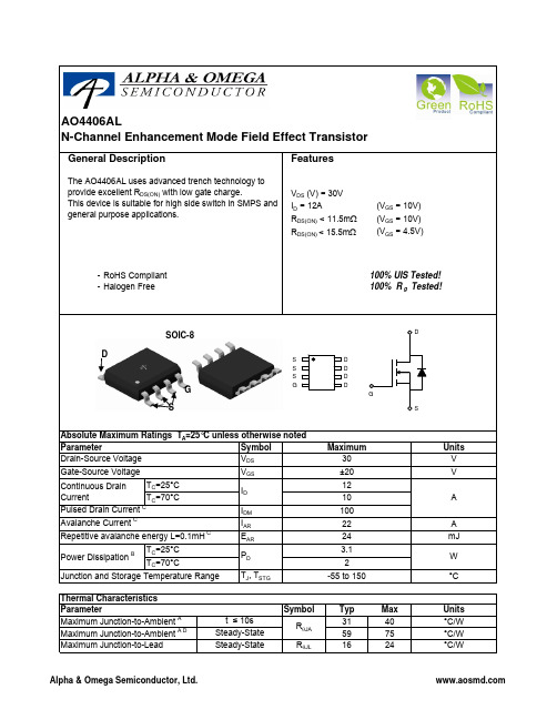
SymbolTyp Max 31405975R θJL 1624Thermal Characteristics t ≤ 10s °C/W ParameterR θJA AO4406ALAbsolute Maximum Ratings T A =25°C unless otherwise noted Maximum Junction-to-LeadSteady-State°C/WSteady-State °C/W Maximum Junction-to-Ambient A D Units Maximum Junction-to-Ambient A SOIC-8G SDSymbolMin TypMaxUnits BV DSS 30V V DS =30V, V GS =0V1T J =55°C5I GSS 100nA V GS(th)Gate Threshold Voltage 1.5 1.92.5V I D(ON)100A 9.511.5T J =125°C141712.515.5m Ωg FS 45S V SD 0.751V I S4A C iss 610760910pF C oss 88125160pF C rss 4070100pF R g0.8 1.6 2.4ΩQ g (10V)111417nC Q g (4.5V)5 6.68nC Q gs 1.9 2.4 2.9nC Q gd 1.83 4.2nC t D(on) 4.4ns t r 9ns t D(off)17ns t f 6ns t rr 5.678ns Q rr6.489.6nCRev 0 : Oct-08COMPONENTS IN LIFE SUPPORT DEVICES OR SYSTEMS ARE NOT AUTHORIZED. AOS DOES NOT ASSUME ANY LIABILITY ARISING OUT OF SUCH APPLICATIONS OR USES OF ITS PRODUCTS. AOS RESERVES THE RIGHT TO IMPROVE PRODUCT DESIGN,FUNCTIONS AND RELIABILITY WITHOUT NOTICE.Body Diode Reverse Recovery Charge I F =12A, dI/dt=500A/µsMaximum Body-Diode Continuous CurrentInput Capacitance Output CapacitanceTurn-On DelayTime DYNAMIC PARAMETERS Turn-On Rise Time Turn-Off DelayTime V GS =10V, V DS =15V, R L =1.25Ω, R GEN =3ΩGate resistanceV GS =0V, V DS =0V, f=1MHzTurn-Off Fall TimeTotal Gate Charge V GS =10V, V DS =15V, I D =12AGate Source Charge Gate Drain Charge Total Gate Charge m ΩI S =1A,V GS =0V V DS =5V, I D =12AV GS =4.5V, I D =10AForward TransconductanceDiode Forward VoltageR DS(ON)Static Drain-Source On-ResistanceI DSS µA V DS =V GS I D =250µA V DS =0V, V GS = ±20V Zero Gate Voltage Drain Current Gate-Body leakage current Electrical Characteristics (T J =25°C unless otherwise noted)STATIC PARAMETERS ParameterConditions Body Diode Reverse Recovery TimeDrain-Source Breakdown Voltage On state drain currentI D =250µA, V GS =0V V GS =10V, V DS =5V V GS =10V, I D =12AReverse Transfer Capacitance I F =12A, dI/dt=500A/µsV GS =0V, V DS =15V, f=1MHz SWITCHING PARAMETERS A. The value of R θJA is measured with the device mounted on 1in 2 FR-4 board with 2oz. Copper, in a still air environment with T A =25°C. The value in any given application depends on the user's specific board design.B. The power dissipation P D is based on T J(MAX)=150°C, using ≤ 10s junction-to-ambient thermal resistance.C. Repetitive rating, pulse width limited by junction temperature T J(MAX)=150°C. Ratings are based on low frequency and duty cycles to keep initialT J =25°C.D. The R θJA is the sum of the thermal impedence from junction to lead R θJL and lead to ambient.E. The static characteristics in Figures 1 to 6 are obtained using <300µs pulses, duty cycle 0.5% max.F. These curves are based on the junction-to-ambient thermal impedence which is measured with the device mounted on 1in 2FR-4 board with 2oz. Copper, assuming a maximum junction temperature of T J(MAX)=150°C. The SOA curve provides a single pulse rating.TYPICAL ELECTRICAL AND THERMAL CHARACTERISTICS11.522.533.54V GS (Volts)Figure 2: Transfer Characteristics (Note E)2040608010012345V DS (Volts)Fig 1: On-Region Characteristics (Note E)I D (A )TYPICAL ELECTRICAL AND THERMAL CHARACTERISTICS2468102468101214Q g (nC)Figure 7: Gate-Charge Characteristics V G S (V o l t s )20040060080010001200051015202530V DS (Volts)Figure 8: Capacitance Characteristics C a p a c i t a n c e (p F )TYPICAL ELECTRICAL AND THERMAL CHARACTERISTICSAO4406ALVdsChargeGate Charge Test Circuit & WaveformResistive Switching Test Circuit & WaveformsVddVdsIdVgsBV I Unclamped Inductive Switching (UIS) Test Circuit & WaveformsARDSS2E = 1/2 LI VddAR AR。
AO9926A中文资料
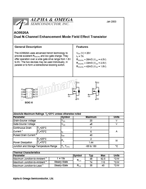
SymbolTyp Max 4862.574110R θJL3540Steady-State °C/W Thermal Characteristics Maximum Junction-to-Lead CSteady-State°C/WParameterUnits Maximum Junction-to-Ambient A t ≤ 10s R θJA °C/W Maximum Junction-to-Ambient A AO9926ASymbolMin TypMaxUnits BV DSS 20V 1T J =55°C5I GSS 100nA V GS(th)0.30.50.8V I D(ON)30A 21.626T J =125°C29.236V GS =2.5V, I D =5A 26.433m Ω33.342m Ωg FS 22S V SD 0.761V I S3A C iss 1050pF C oss 163pF C rss 129pF R g4ΩQ g 15.2nC Q gs 1nC Q gd 4nC t D(on) 6.5ns t r 9ns t D(off)56.5ns t f 13.2ns t rr Body Diode Reverse Recovery time21ns Q rrBody Diode Reverse Recovery charge 7.1nCI F =5A, dI/dt=100A/µsI F =5A, dI/dt=100A/µsElectrical Characteristics (T J =25°C unless otherwise noted)ParameterConditions STATIC PARAMETERS Drain-Source Breakdown Voltage I D =250µA, V GS =0V I DSS Zero Gate Voltage Drain Current V DS =16V, V GS =0VµA Gate-Body leakage current V DS =0V, V GS =±8V Gate Threshold Voltage V DS =V GS I D =250µA On state drain currentV GS =4.5V, V DS =5V R DS(ON)Static Drain-Source On-ResistanceV GS =4.5V, I D =7Am ΩV GS =1.8V, I D =4AV GS =0V, V DS =0V, f=1MHzForward TransconductanceV DS =5V, I D =5ADiode Forward Voltage I S =1A Maximum Body-Diode Continuous CurrentDYNAMIC PARAMETERS Input Capacitance V GS =0V, V DS =10V, f=1MHz Output Capacitance Reverse Transfer Capacitance Turn-On Rise Time Turn-Off DelayTime Gate resistanceTurn-Off Fall TimeSWITCHING PARAMETERS Total Gate Charge V GS =4.5V, V DS =10V, I D =7AGate Source Charge Gate Drain Charge Turn-On DelayTime V GS =5V, V DS =10V, R L =1.5Ω, R GEN =3ΩA: The value of R θJA is measured with the device mounted on 1in 2FR-4 board with 2oz. Copper, in a still air environment with T A =25°C. The value in any a given application depends on the user's specific board design. The current rating is based on the t ≤ 10s thermal resistance rating.B: Repetitive rating, pulse width limited by junction temperature.C. The R θJA is the sum of the thermal impedence from junction to lead R θJL and lead to ambient.D. The static characteristics in Figures 1 to 6 are obtained using 80 µs pulses, duty cycle 0.5% max.E. These tests are performed with the device mounted on 1 in 2FR-4 board with 2oz. Copper, in a still air environment with T A =25°C. The SOA curve provides a single pulse rating.。
谐音的网络用语英语
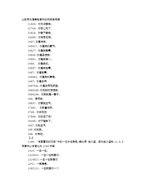
以数字为谐音或象形的网络常用语01925:你依旧爱我。
02746:你恶心死了.02825:你爱不爱我。
03456:你相思无用。
0437:你是神经。
045617:你是我的氧气。
04527:你是我爱妻。
04535:你是否想我。
04551:你是我唯一。
0456:你是我的。
04567:你是我老妻。
0457:你是我妻。
045692:你是我的最爱。
0487:你是白痴.0487561:你是白痴无药医。
0564335:你无聊时想想我。
0594184:你我就是一辈子。
065:原谅我.06537:你惹我生气。
07382:你欺善怕恶。
0748:你去死吧.07868:你吃饱了吗?08056:你不理我了。
0837:你别生气.095:你找我。
098:你走吧。
【1】1096:“凉宫春日的忧郁”中的一位女性角色,朝比奈实久留,因为实久留和10,9,6同音所以被简化为1096书写1314:一生一世。
1314920:一生一世就爱你。
1314520:一生一世我爱你1372:一厢情愿。
1392010:一生就爱你一个.1414:要死要死。
意思意思.147:一世情。
1573:一往情深.1589854:要我发,就发五次.1711:一心一意.177155:miss。
(这个不是谐音,是象形)1920:依旧爱你。
1930:依旧想你。
【2】200:爱你哦.20110:爱你一百一十年。
20184:爱你一辈子.2030999:爱你想你久久久。
2037:为你伤心.20475:爱你是幸福。
20609:爱你到永久.20863:爱你到来生。
220225:爱爱你爱爱我。
230:爱死你。
234:爱相随。
235:要想你。
2406:爱死你啦。
246:饿死了.246437:爱是如此神奇.25184:爱我一辈子.25873:爱我到今生。
25910:爱我久一点。
25965:爱我就留我.259695:爱我就了解我.259758:爱我就娶我吧.2627:爱来爱去。
282:饿不饿。
4046中文资料
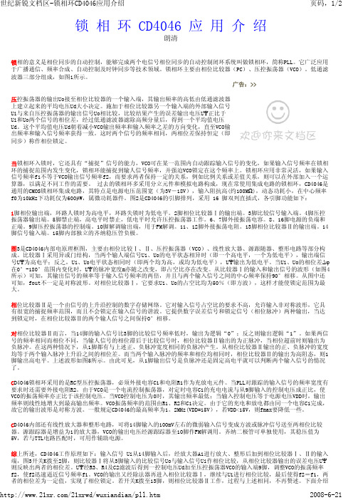
锁 相 环 CD4046 应 用 介 绍朗清锁相的意义是相位同步的自动控制,能够完成两个电信号相位同步的自动控制闭环系统叫做锁相环,简称PLL。
它广泛应用于广播通信、频率合成、自动控制及时钟同步等技术领域。
锁相环主要由相位比较器(PC)、压控振荡器(VCO)。
低通滤波器三部分组成,如图1所示。
广告:>>上建立起来的平均电压Ud大小决定。
施加于相位比较器另一个输入端的外部输入信号Ui与来自压控振荡器的输出信号Uo相比较,比较结果产生的误差输出电压UΨ正比于Ui和Uo两个信号的相位差,经过低通滤波器滤除高频分量后,得到一个平均值电压Ud。
这个平均值电压Ud朝着减小VCO输出频率和输入频率之差的方向变化,直至VCO输出频率和输入信号频率获得一致。
这时两个信号的频率相同,两相位差保持恒定(即同步)称作相位锁定。
当锁相环入锁时,它还具有“捕捉”信号的能力,VCO可在某一范围内自动跟踪输入信号的变化,如果输入信号频率在锁相环的捕捉范围内发生变化,锁相环能捕捉到输人信号频率,并强迫VCO锁定在这个频率上。
锁相环应用非常灵活,如果输入信号频率f1不等于VCO输出信号频率f2,而要求两者保持一定的关系,例如比例关系或差值关系,则可以在外部加入一个运算器,以满足不同工作的需要。
过去的锁相环多采用分立元件和模拟电路构成,现在常使用集成电路的锁相环,CD4046是通用的CMOS锁相环集成电路,其特点是电源电压范围宽(为3V-18V),输入阻抗高(约100MΩ),动态功耗小,在中心频率f0为10kHz下功耗仅为600μW,属微功耗器件。
图2是CD4046的引脚排列,采用 16 脚双列直插式,各引脚功能如下:1脚相位输出端,环路人锁时为高电平,环路失锁时为低电平。
2脚相位比较器Ⅰ的输出端。
3脚比较信号输入端。
4脚压控振荡器输出端。
5脚禁止端,高电平时禁止,低电平时允许压控振荡器工作。
6、7脚外接振荡电容。
8、16脚电源的负端和正端。
场效应管知识集锦
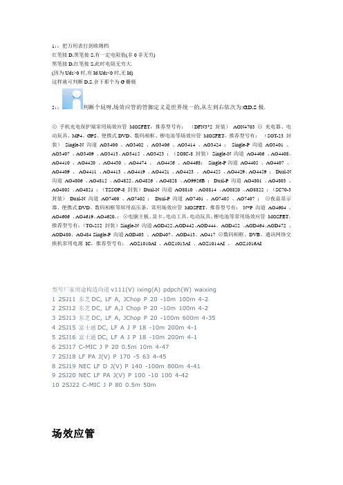
1::把万用表打到欧姆档红笔接D,黑笔接S,有一定电阻值(非0非无穷)黑笔接D,红笔接S,此时电阻无穷大.(因为Uds>0时,有Id.Uds<0时,无Id)这样就可判断D,S.余下那个为G栅极2::判断个屁呀,场效应管的管脚定义是世界统一的,从左到右依次为:G,D,S极.⊙手机充电保护端常用场效应管MOSFET,推荐型号有:(DFN3*2 封装)AON4703 ⊙充电器、电动玩具、MP4、GPS、便携式DVD、数码相框、锂电池等场效应管MOSFET,推荐型号有:(SOT-23 封装)Single-N 沟道AO3400 、AO3402 、AO3406 、AO3414 、AO3424 ;Single-P 沟道AO3401 、AO3407 、AO3409 、AO3413、AO3415 、AO3423 ;(SOIC-8 封装)Single-N 沟道AO4406 、AO4408、AO4410 、AO4420 、AO4430 、AO4474 、AO4456 、AO4468;Single-P沟道AO4405 、AO4407 、AO4409 、AO4411 、AO4413 、AO4419 、AO4421 、AO4423 、AO4425 、AO4429、AO4459 ;Dual-N 沟道AO4806 、AO4812 、AO4822、AO4826 、AO4828 、AO9926B ;Dual-P 沟道AO4801 、AO4803 、AO4805 、AO4821 ;(TSSOP-8 封装)Dual-N 沟道AO8810 、AO8814 、AO8820 、AO8822 ;(SC70-3 封装)Dual-N 沟道AO7400 、AO7402 ;Dual-P 沟道AO7401 、AO7405 、AO7407 ;⊙夜晶显示器、便携式DVD、数码相框等屏用高压条,常用场效应管MOSFET,推荐型号有:N+P 沟道AO4604 、AO4606 、AO4619、AO4620、;⊙电脑主板、显卡、电动工具、电动玩具、锂电池等常用场效应管MOSFET,推荐型号有:(TO-252 封装)Single-N 沟道AOD422、AOD442、AOD444、AOD452 、AOD464、AOD472 、AOD480、AO484 Single-P 沟道AOD403 、AOD407、AOD413、AO417 ⊙数码相框、DVB、通讯网络交换机常用电源IC,推荐型号有:AOZ1010AI 、AOZ1013AI 、AOZ1014AI 、AOZ1016AI型号厂家用途构造沟道v111(V) ixing(A) pdpch(W) waixing1 2SJ11 东芝DC, LF A, JChop P 20 -10m 100m 4-22 2SJ12 东芝DC, LF A,J Chop P 20 -10m 100m 4-23 2SJ13 东芝DC, LF A, JChop P 20 -100m 600m 4-354 2SJ15 富士通DC, LF A J P 18 -10m 200m 4-15 2SJ16 富士通DC, LF A J P 18 -10m 200m 4-16 2SJ17 C-MIC J P 20 0.5m 10m 4-477 2SJ18 LF PA J(V) P 170 -5 63 4-458 2SJ19 NEC LF D J(V) P 140 -100m 800m 4-419 2SJ20 NEC LF PA J(V) P 100 -10 100 4-4210 2SJ22 C-MIC J P 80 0.5m 50m场效应管根据三极管的原理开发出的新一代放大元件,有3个极性,栅极,漏极,源极,它的特点是栅极的内阻极高,采用二氧化硅材料的可以达到几百兆欧,属于电压控制型器件。
常用三极管参数大全

玉林万顺达电脑芯片级维修资料 2010-07-20整理玉林万顺达电脑芯片级维修资料 2010-07-20整理玉林万顺达电脑芯片级维修资料 2010-07-20整理玉林万顺达电脑芯片级维修资料 2010-07-20整理玉林万顺达电脑芯片级维修资料 2010-07-20整理玉林万顺达电脑芯片级维修资料 2010-07-20整理玉林万顺达电脑芯片级维修资料 2010-07-20整理玉林万顺达电脑芯片级维修资料 2010-07-20整理玉林万顺达电脑芯片级维修资料 2010-07-20整理玉林万顺达电脑芯片级维修资料 2010-07-20整理玉林万顺达电脑芯片级维修资料 2010-07-20整理玉林万顺达电脑芯片级维修资料 2010-07-20整理玉林万顺达电脑芯片级维修资料 2010-07-20整理玉林万顺达电脑芯片级维修资料 2010-07-20整理玉林万顺达电脑芯片级维修资料 2010-07-20整理玉林万顺达电脑芯片级维修资料 2010-07-20整理玉林万顺达电脑芯片级维修资料 2010-07-20整理玉林万顺达电脑芯片级维修资料 2010-07-20整理玉林万顺达电脑芯片级维修资料 2010-07-20整理玉林万顺达电脑芯片级维修资料 2010-07-20整理玉林万顺达电脑芯片级维修资料 2010-07-20整理玉林万顺达电脑芯片级维修资料 2010-07-20整理玉林万顺达电脑芯片级维修资料 2010-07-20整理玉林万顺达电脑芯片级维修资料 2010-07-20整理玉林万顺达电脑芯片级维修资料 2010-07-20整理玉林万顺达电脑芯片级维修资料 2010-07-20整理玉林万顺达电脑芯片级维修资料 2010-07-20整理玉林万顺达电脑芯片级维修资料 2010-07-20整理玉林万顺达电脑芯片级维修资料 2010-07-20整理玉林万顺达电脑芯片级维修资料 2010-07-20整理。
AO4466资料
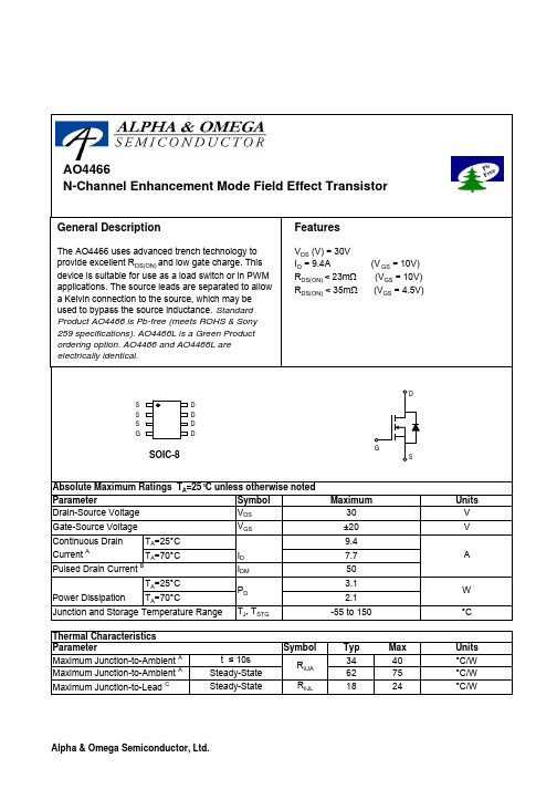
Symbol Typ Max 34406275R θJL 1824Maximum Junction-to-Lead C Steady-State °C/W Thermal CharacteristicsParameterUnits Maximum Junction-to-Ambient At ≤ 10s R θJA °C/W °C/W Maximum Junction-to-Ambient ASteady-State AO4466AO4466Symbol Min Typ Max Units BV DSS 30V 0.0041T J =55°C 5I GSS100nA V GS(th)1 1.63V I D(ON)20A 1723T J =125°C 24302735m Ωg FS1024S V SD0.751V I S 4.3A C iss 621820pF C oss 118pF C rss 85pF R g 0.81.5ΩQ g (10V)11.317nC Q g (4.5V) 5.78nC Q gs 2.1nC Q gd 3nC t D(on) 4.56.5ns t r 3.15ns t D(off)15.123ns t f 2.75ns t rr 15.521ns Q rr 7.110nC THIS PRODUCT HAS BEEN DESIGNED AND QUALIFIED FOR THE CONSUMER MARKET. APPLICATIONS OR USES AS CRITICALCOMPONENTS IN LIFE SUPPORT DEVICES OR SYSTEMS ARE NOT AUTHORIZED. AOS DOES NOT ASSUME ANY LIABILITY ARISING OUT OF SUCH APPLICATIONS OR USES OF ITS PRODUCTS. AOS RESERVES THE RIGHT TO IMPROVE PRODUCT DESIGN,FUNCTIONS AND RELIABILITY WITHOUT NOTICE.Body Diode Reverse Recovery Time Body Diode Reverse Recovery Charge I F =9.4A, dI/dt=100A/µsDrain-Source Breakdown VoltageOn state drain current I D =250µA, V GS =0V V GS =4.5V, V DS =5V V GS =10V, I D =9.4A Reverse Transfer Capacitance I F =9.4A, dI/dt=100A/µs Electrical Characteristics (T J =25°C unless otherwise noted)STATIC PARAMETERSParameter Conditions I DSSµA Gate Threshold Voltage V DS =V GS I D =250µA V DS =24V, V GS =0V V DS =0V, V GS = ±20V Zero Gate Voltage Drain Current Gate-Body leakage current R DS(ON)Static Drain-Source On-Resistance Forward Transconductance Diode Forward Voltage m ΩV GS =4.5V, I D =5A I S =1A,V GS =0V V DS =5V, I D =9.4A Total Gate Charge Gate Source Charge Gate resistance V GS =0V, V DS =0V, f=1MHz Turn-On Rise Time Turn-Off DelayTime V GS =10V, V DS =15V, R L =1.6Ω,R GEN =3ΩTurn-Off Fall Time Maximum Body-Diode Continuous Current Input Capacitance Output Capacitance Turn-On DelayTime DYNAMIC PARAMETERS V GS =10V, V DS =15V, I D =9.4A Total Gate Charge Gate Drain Charge V GS =0V, V DS =15V, f=1MHzSWITCHING PARAMETERS A: The value of R θJA is measured with the device mounted on 1in 2 FR-4 board with 2oz. Copper, in a still air environment with T A =25°C. The value in any given application depends on the user's specific board design. The current rating is based on the t ≤ 10s thermal resistance rating.B: Repetitive rating, pulse width limited by junction temperature.C. The R θJA is the sum of the thermal impedence from junction to lead R θJL and lead to ambient.D. The static characteristics in Figures 1 to 6 are obtained using 80 µs pulses, duty cycle 0.5% max.E. These tests are performed with the device mounted on 1 in 2 FR-4 board with 2oz. Copper, in a still air environment with T A =25°C. The SOA curve provides a single pulse rating.Rev 0: Apr. 2006AO4466AO4466。
AO4410中文资料

SymbolTyp Max 31405975R θJL 1624Maximum Junction-to-Ambient A Steady-State °C/W Maximum Junction-to-Lead CSteady-State°C/WThermal Characteristics ParameterUnits Maximum Junction-to-Ambient A t ≤ 10s R θJA °C/W AO4410AO4410SymbolMin TypMaxUnits BV DSS 30V 0.0051T J =55°C5I GSS 100nA V GS(th)0.8 1.11.5V I D(ON)80A 4.7 5.5T J =125°C6.47.45.2 6.2m Ωg FS 102S V SD 0.641V I S4.5A C iss 913010500pF C oss 625pF C rss 387pF R g0.40.5ΩQ g (4.5V)72.485nC Q gs 13.4nC Q gd 16.8nC t D(on)1115ns t r 711ns t D(off)99135ns t f 1319.5ns t rr 3340ns Q rr22.230nCTHIS PRODUCT HAS BEEN DESIGNED AND QUALIFIED FOR THE CONSUMER MARKET. APPLICATIONS OR USES AS CRITICAL COMPONENTS IN LIFE SUPPORT DEVICES OR SYSTEMS ARE NOT AUTHORIZED. AOS DOES NOT ASSUME ANY LIABILITY ARISING OUT OF SUCH APPLICATIONS OR USES OF ITS PRODUCTS. AOS RESERVES THE RIGHT TO IMPROVE PRODUCT DESIGN,FUNCTIONS AND RELIABILITY WITHOUT NOTICE.Body Diode Reverse Recovery TimeBody Diode Reverse Recovery Charge I F =18A, dI/dt=100A/µsDrain-Source Breakdown Voltage On state drain currentI D =250µA, V GS =0V V GS =4.5V, V DS =5V V GS =10V, I D =18AReverse Transfer Capacitance I F =18A, dI/dt=100A/µsElectrical Characteristics (T J =25°C unless otherwise noted)STATIC PARAMETERS ParameterConditions I DSS µA Gate Threshold Voltage V DS =V GS I D =250µA V DS =24V, V GS =0VV DS =0V, V GS = ±12V Zero Gate Voltage Drain Current Gate-Body leakage current R DS(ON)Static Drain-Source On-ResistanceForward TransconductanceDiode Forward Voltage Maximum Body-Diode Continuous CurrentInput Capacitance Output Capacitance DYNAMIC PARAMETERS m ΩV GS =4.5V, I D =15AI S =1A,V GS =0V V DS =5V, I D =18ATurn-On Rise Time Turn-Off DelayTime V GS =10V, V DS =15V, R L =0.83Ω, R GEN =3ΩTurn-Off Fall TimeTurn-On DelayTime Gate Drain Charge V GS =0V, V DS =15V, f=1MHz SWITCHING PARAMETERS Total Gate Charge Gate Source Charge Gate resistanceV GS =0V, V DS =0V, f=1MHzV GS =10V, V DS =15V, I D =18AA: The value of R θJA is measured with the device mounted on 1in 2 FR-4 board with 2oz. Copper, in a still air environment with T A =25°C. The value in any given application depends on the user's specific board design. The current rating is based on the t ≤ 10s thermal resistance rating.B: Repetitive rating, pulse width limited by junction temperature.C. The R θJA is the sum of the thermal impedence from junction to lead R θJL and lead to ambient.D. The static characteristics in Figures 1 to 6 are obtained using 80 µs pulses, duty cycle 0.5% max.E. These tests are performed with the device mounted on 1 in 2FR-4 board with 2oz. Copper, in a still air environment with T A =25°C. The SOA curve provides a single pulse rating. Rev 4 : May 2005AO4410AO4410。
A43L2616AV-6中文资料

Preliminary 1M X 16 Bit X 4 Banks Synchronous DRAMDocument Title1M X 16 Bit X 4 Banks Synchronous DRAMRevision HistoryDate Remark Rev. No. History Issue issue November 30, 2004 Preliminary0.0 InitialA43L2616APreliminary1M X 16 Bit X 4 Banks Synchronous DRAMFeatureJEDEC standard 3.3V power supplyLVTTL compatible with multiplexed address Four banks / Pulse RAS MRS cycle with address key programs - CAS Latency (2,3)- Burst Length (1,2,4,8 & full page) - Burst Type (Sequential & Interleave) All inputs are sampled at the positive going edge of the system clock Clock Frequency: 166MHz @ CL=3 143MHz @ CL=3Burst Read Single-bit Write operationDQM for masking Auto & self refresh 64ms refresh period (4K cycle) Commercial Temperature Operation : 0°C~70°C Industrial Temperature Operation : -40°C~85°C for –U grade 54 Pin TSOP (II) and 54 Balls CSP (8mm x 8mm)General DescriptionThe A43L2616A is 67,108,864 bits synchronous high data rate Dynamic RAM organized as 4 X 1,048,576 words by 16 bits, fabricated with AMIC’s high performance CMOS technology. Synchronous design allows precise cycle control with the use of system clock.I/O transactions are possible on every clock cycle. Range of operating frequencies, programmable latencies allows the same device to be useful for a variety of high bandwidth, high performance memory system applications.Pin ConfigurationTSOP (II)V S SD Q 15V S S QD Q 14D Q 13V D D QD Q 12D Q 11V S S QD Q 10D Q 9V D D QD Q 8V S SU D Q MC KC K EN CA 9A 8A 7A 6A 5A 4V S SV D DD Q 0V D D QD Q 1D Q 2V S S QD Q 3D Q 4V D D QD Q 5D Q 6V S S QD Q 7V D DL D Q MW EC A SR A SC SA 10/A PB S 1B S 0A 0A 1A 2A 3V D DA 11N CPin Configuration (continued)54 Balls CSP (8 mm x 8 mm)Top ViewBlock DiagramCLKADDDQiPin DescriptionsAbsolute Maximum Ratings*Voltage on any pin relative to VSS (Vin, Vout ) . . . . . . . . .. . . . . . . . . . . . . . . . . . . . . . . . . . . . . . . . . . -1.0V to +4.6V Voltage on VDD supply relative to VSS (VDD, VDDQ ) . . . . . . . . . . . . . . . . . . . . . . . . . . . . . . . . . . .-1.0V to +4.6V Storage Temperature (T STG ) . . . . . . . . . . -55°C to +150°C Soldering Temperature X Time (T SLODER ) . . . . . . . . . . . . . . . . . . . . . . . . . . . . . . . . . . . . . . . . . . . . . . . . 260°C X 10sec Power Dissipation (P D ) . . . . . . . . . . . . . . . . . . . . . . . . .1W Short Circuit Current (Ios) . . . . . . . . . . . . . . . . . . . . 50mA *CommentsPermanent device damage may occur if “Absolute Maximum Ratings” are exceeded.Functional operation should be restricted to recommended operating condition.Exposure to higher than recommended voltage for extended periods of time could affect device reliability.Capacitance (T A =25°C, f=1MHz)DC Electrical CharacteristicsRecommend operating conditions (Voltage referenced to VSS = 0V, T A = 0ºC to +70ºC or T A = -40ºC to +85ºC)Parameter Symbol Min Typ Max Unit NoteSupply Voltage VDD,VDDQ 3.0 3.3 3.6 VInput High Voltage V IH 2.0 3.0 VDD+0.3 VInput Low Voltage V IL -0.3 0 0.8 V Note 1 Output High Voltage V OH 2.4 --V I OH = -2mAOutput Low Voltage V OL - - 0.4 V I OL = 2mA Input Leakage Current I IL -5 - 5 µA Note 2 Output Leakage Current I OL -5 - 5 µANote 3Output Loading ConditionSee Figure 1Note: 1. V IL (min) = -1.5V AC (pulse width ≤ 5ns).2. Any input 0V ≤ VIN ≤ VDD + 0.3V, all other pins are not under test = 0V3. Dout is disabled, 0V ≤ Vout ≤ VDDDecoupling Capacitance Guide LineRecommended decoupling capacitance added to power line at board.Parameter Symbol Value UnitDecoupling Capacitance between VDD and VSS C DC1 0.1 + 0.01 µF Decoupling Capacitance between VDDQ and VSSQC DC20.1 + 0.01µFNote: 1. VDD and VDDQ pins are separated each other.All VDD pins are connected in chip. All VDDQ pins are connected in chip. 2. VSS and VSSQ pins are separated each otherAll VSS pins are connected in chip. All VSSQ pins are connected in chip.DC Electrical Characteristics(Recommended operating condition unless otherwise noted, T A = 0°C to 70°C T A = -40ºC to +85ºC) Note: 1. Measured with outputs open. Addresses are changed only one time during t CC (min).2. Refresh period is 64ms. Addresses are changed only one time during t CC (min).3. I CC6 normal version: A43L2616AV-6, A43L2616AV-7.4. I CC6 low self refresh current version: A43L2616AV-6V, A43L2616AV-7V.AC Operating Test Conditions(VDD = 3.3V ±0.3V, T A = 0°C to +70°C or T A = -40ºC to +85ºC)Parameter ValueAC input levelsV IH /V IL = 2.4V/0.4V Input timing measurement reference level 1.4VInput rise and all time (See note3)tr/tf = 1ns/1ns Output timing measurement reference level 1.4V Output load conditionSee Fig.2Output(Fig. 1) DC Output Load Circuit ΩTT =1.4V (Fig. 2) AC Output Load CircuitAC Characteristics(AC operating conditions unless otherwise noted)-6 -7Symbol Parameter CAS Latency Min Max Min MaxUnit Notet CC CLK cycle time 6 1000 7 1000 ns 1t SACCLK to valid Output delay- 5 - 5.4 ns 1,2 t OH Output data hold time 2.5-2.7-ns2t CH CLK high pulse width 32.5 - 2.5 - ns 3 t CL CLK low pulse width 2.5 - 2.5 - ns 3 t SS Input setup time 2 - 2 - ns 3 t SH Input hold time 1 - 1 - ns 3 t SLZ CLK to output in Low-Z 1-1-ns2t SHZCLK to output In Hi-Z3- 5.5 - 6 ns*All AC parameters are measured from half to half.Note : 1. Parameters depend on programmed CAS latency.2. If clock rising time is longer than 1ns, (tr/2-0.5) ns should be added to the parameter.3. Assumed input rise and fall time (tr & tf) = 1ns.If tr & tf is longer than 1ns, transient time compensation should be considered, i.e., [(tr + tf)/2-1]ns should be added to the parameter.Operating AC Parameter(AC operating conditions unless otherwise noted)Note: 1. The minimum number of clock cycles is determined by dividing the minimum time required with clock cycle time and then rounding off to the next higher integer.2. Minimum delay is required to complete write.Simplified Truth Table(V = Valid, X = Don’t Care, H = Logic High, L = Logic Low) Note : 1. OP Code: Operand CodeA0~A11, BS0, BS1: Program keys. (@MRS)2. MRS can be issued only at both banks precharge state.A new command can be issued after 2 clock cycle of MRS.3. Auto refresh functions as same as CBR refresh of DRAM.The automatical precharge without Row precharge command is meant by “Auto”.Auto/Self refresh can be issued only at both precharge state.4. BS0, BS1 : Bank select address.If both BS1 and BS0 are “Low” at read, write, row active and precharge, bank A is selected.If both BS1 is “Low” and BS0 is “High” at read, write, row active and precharge, bank B is selected.If both BS1 is “High” and BS0 is “Low” at read, write, row active and precharge, bank C is selected.If both BS1 and BS0 are “High” at read, write, row active and precharge, bank D is selected.If A10/AP is “High” at row precharge, BS1 and BS0 is ignored and all banks are selected.5. During burst read or write with auto precharge, new read write command cannot be issued.Another bank read write command can be issued at every burst length.6. DQM sampled at positive going edge of a CLK masks the data-in at the very CLK (Write DQM latency is 0) butmasks the data-out Hi-Z state after 2 CLK cycles. (Read DQM latency is 2)Mode Register Filed Table to Program ModesRegister Programmed with MRS AddressBS0, BS1A11, A10A9A8A7A6A5A4A3A2A1A0FunctionRFURFU W.B.L TM CAS Latency BT Burst Length(Note 1)(Note 2)Test ModeCAS LatencyBurst TypeBurst LengthA8 A7TypeA6 A5 A4Latency A3TypeA2A1 A0 BT=0BT=10 0 Mode Register Set0 0 0Reserved0Sequential 00 0 1 1 0 1 0 0 1- 1Interleave 00 1 2 2 1 0 0 1 0 2 0 1 0 4 4 1 1Vendor Use Only0 1 1 3 0 1 188 Write Burst Length 1 0 0Reserved 10 0 Reserved Reserved A9 Length 1 0 1Reserved10 1 ReservedReserved0 Burst 1 1 0Reserved 1 1 0 Reserved Reserved 1 Single Bit 1 1 1Reserved11 1 256(Full)ReservedPower Up Sequence1. Apply power and start clock, Attempt to maintain CKE = “H”, DQM = “H” and the other pins are NOP condition at inputs.2. Maintain stable power, stable clock and NOP input condition for a minimum of 200µs.3. Issue precharge commands for all banks of the devices.4. Issue 2 or more auto-refresh commands.5. Issue a mode register set command to initialize the mode register. cf.) Sequence of 4 & 5 may be changed.The device is now ready for normal operation.Note : 1. RFU(Reserved for Future Use) should stay “0” during MRS cycle.2. If A9 is high during MRS cycle, “Burst Read Single Bit Write” function will be enabled.Burst Sequence (Burst Length = 4)Initial addressSequential Interleave A1 A00 0 0 1 2 3 0 1 2 30 1 1 2 3 0 1 0 3 21 023 0 1 2 3 0 11 1 3 0 123 2 1 0Burst Sequence (Burst Length = 8)Initial addressSequential Interleave A2 A1 A00 0 0 0 1 2 3 4 5 6 7 0 1 2 3 4 5 6 70 0 1 1 2 3 4 5 6 7 0 1 0 3 2 5 4 7 60 1 0 2 3 4 5 6 7 0 1 2 3 0 1 6 7 4 50 1 1 3 4 5 6 7 0 1 2 3 2 1 0 7 6 5 41 0 0 4 5 6 7 0 1234567 0 1 2 31 0 1 5 6 7 0 12345 4 76 1 0 3 21 1 0 6 7 0 1234567 4 5 2 3 0 11 1 1 7 0 1234567 6 5 4 3 2 1 0Device OperationsClock (CLK)The clock input is used as the reference for all SDRAM operations. All operations are synchronized to the positive going edge of the clock. The clock transitions must be monotonic between V IL and V IH. During operation with CKE high all inputs are assumed to be in valid state (low or high) for the duration of set up and hold time around positive edge of the clock for proper functionality and ICC specifications.Clock Enable (CLK)The clock enable (CKE) gates the clock onto SDRAM. If CKE goes low synchronously with clock (set-up and hold time same as other inputs), the internal clock is suspended form the next clock cycle and the state of output and burst address is frozen as long as the CKE remains low. All other inputs are ignored from the next clock cycle after CKE goes low. When both banks are in the idle state and CKE goes low synchronously with clock, the SDRAM enters the power down mode form the next clock cycle. The SDRAM remains in the power down mode ignoring the other inputs as long as CKE remains low. The power down exit is synchronous as the internal clock is suspended. When CKE goes high at least “t SS + 1 CLOCK” before the high going edge of the clock, then the SDRAM becomes active from the same clock edge accepting all the input commands.Bank Select (BS0, BS1)This SDRAM is organized as 4 independent banks of 1,048,576 words X 16 bits memory arrays. The BS0, BS1 inputs is latched at the time of assertion of RAS and CASto select the bank to be used for the operation. The bank select BS0, BS1 is latched at bank activate, read, write mode register set and precharge operations.Address Input (A0 ~ A11)The 20 address bits required to decode the 262,144 word locations are multiplexed into 12 address input pins (A0~A11). The 12 bit row address is latched along with RAS, BS0 and BS1 during bank activate command. The 8 bit column address is latched along with CAS, WE, BS0 and BS1during read or write command.NOP and Device DeselectWhen , CAS and WE are high, the SDRAM performs no operation (NOP). NOP does not initiate any new operation, but is needed to complete operations which require more than single clock like bank activate, burst read, auto refresh, etc. The device deselect is also a NOP and is entered by asserting CS high. CS high disables the command decoder so that RAS, CAS and WE, and all the address inputs are ignored.Power-UpThe following sequence is recommended for POWER UP 1. Power must be applied to either CKE and DQM inputs topull them high and other pins are NOP condition at the inputs before or along with VDD (and VDDQ) supply.The clock signal must also be asserted at the same time.2. After VDD reaches the desired voltage, a minimumpause of 200 microseconds is required with inputs in NOP condition.3. Both banks must be precharged now.4. Perform a minimum of 2 Auto refresh cycles to stabilizethe internal circuitry.5. Perform a MODE REGISTER SET cycle to program theCAS latency, burst length and burst type as the default value of mode register is undefined.At the end of one clock cycle from the mode register set cycle, the device is ready for operation.When the above sequence is used for Power-up, all the out-puts will be in high impedance state. The high impedance of outputs is not guaranteed in any other power-up sequence.cf.) Sequence of 4 & 5 may be changed.Mode Register Set (MRS)The mode register stores the data for controlling the various operation modes of SDRAM. It programs the CAS latency, addressing mode, burst length, test mode and various vendor specific options to make SDRAM useful for variety of different applications. The default value of the mode register is not defined, therefore the mode register must be written after power up to operate the SDRAM. The mode register is written by asserting low on CS,RAS, CAS,(The SDRAM should be in active mode with CKE already high prior to writing the mode register). The state of address pins A0~A11, BS0 and BS1 in the same cycle as CS,,CAS,WE going low is the data written in the mode register. One clock cycle is required to complete the write in the mode register. The mode register contents can be changed using the same command and clock cycle requirements during operation as long as both banks are in the idle state. The mode register is divided into various fields depending on functionality. The burst length field uses A0~A2, burst type uses A3, addressing mode uses A4~A6, A7~A8, A11, BS0 and BS1 are used for vendor specific options or test mode. And the write burst length is programmed using A9. A7~A8, A11, BS0 and BS1 must be set to low for normal SDRAM operation.Refer to table for specific codes for various burst length, addressing modes and CAS latencies.Device Operations (continued)Bank ActivateThe bank activate command is used to select a random row in an idle bank. By asserting low on RAS and CS with desired row and bank addresses, a row access is initiated. The read or write operation can occur after a time delay of t RCD(min) from the time of bank activation. t RCD(min) is an internal timing parameter of SDRAM, therefore it is dependent on operating clock frequency. The minimum number of clock cycles required between bank activate and read or write command should be calculated by dividing t RCD(min) with cycle time of the clock and then rounding off the result to the next higher integer. The SDRAM has two internal banks on the same chip and shares part of the internal circuitry to reduce chip area, therefore it restricts the activation of both banks immediately. Also the noise generated during sensing of each bank of SDRAM is high requiring some time for power supplies recover before the other bank can be sensed reliably. t RRD(min) specifies the minimum time required between activating different banks. The number of clock cycles required between different bank activation must be calculated similar to t RCD specification. The minimum time required for the bank to be active to initiate sensing and restoring the complete row of dynamic cells is determined by t RAS(min) specification before a precharge command to that active bank can be asserted. The maximum time any bank can be in the active state is determined by t RAS(max). The number of cycles for both t RAS(min) and t RAS(max) can be calculated similar to t RCD specification.Burst ReadThe burst read command is used to access burst of data on consecutive clock cycles from an active row in an active bank. The burst read command is issued by asserting low on CS and CAS with WE being high on the positive edge of the clock. The bank must be active for at least t RCD(min) before the burst read command is issued. The first output appears CAS latency number of clock cycles after the issue of burst read command. The burst length, burst sequence and latency from the burst read command is determined by the mode register which is already programmed. The burst read can be initiated on any column address of the active row. The address wraps around if the initial address does not start from a boundary such that number of outputs from each I/O are equal to the burst length programmed in the mode register. The output goes into high-impedance at the end of the burst, unless a new burst read was initiated to keep the data output gapless. The burst read can be terminated by issuing another burst read or burst write in the same bank or the other active bank or a precharge command to the same bank. The burst stop command is valid at every page burst length. Burst WriteThe burst write command is similar to burst read command, and is used to write data into the SDRAM consecutive clock cycles in adjacent addresses depending on burst length and burst sequence. By asserting low on CS,CAS and WE with valid column address, a write burst is initiated. The data inputs are provided for the initial address in the same clock cycle as the burst write command. The input buffer is deselected at the end of the burst length, even though the internal writing may not have been completed yet. The writing can not complete to burst length. The burst write can be terminated by issuing a burst read and DQM for blocking data inputs or burst write in the same or the other active bank. The burst stop command is valid only at full page burst length where the writing continues at the end of burst and the burst is wrap around. The write burst can also be terminated by using DQM for blocking data and precharging the bank “t RDL” after the last data input to be written into the active row. See DQM OPERATION also.DQM OperationThe DQM is used to mask input and output operation. It works similar to OE during read operation and inhibits writing during write operation. The read latency is two cycles from DQM and zero cycle for write, which means DQM masking occurs two cycles later in the read cycle and occurs in the same cycle during write cycle. DQM operation is synchronous with the clock, therefore the masking occurs for a complete cycle. The DQM signal is important during burst interrupts of write with read or precharge in the SDRAM. Due to asynchronous nature of the internal write, the DQM operation is critical to avoid unwanted or incomplete writes when the complete burst write is not required.PrechargeThe precharge operation is performed on an active bank by asserting low on CS,RAS,WE and A10/AP with valid BA of the bank to be precharged. The precharge command can be asserted anytime after t RAS(min) is satisfied from the bank activate command in the desired bank. “t RP” is defined as the minimum time required to precharge a bank. The minimum number of clock cycles required to complete row precharge is calculated by dividing “t RP” with clock cycle time and rounding up to the next higher integer. Care should be taken to make sure that burst write is completed or DQM is used to inhibit writing before precharge command is asserted. The maximum time any bank can be active is specified by t RAS(max). Therefore, each bank has to be precharged within t RAS(max) from the bank activate command. At the end of precharge, the bank enters the idle state and is ready to be activated again.Entry to Power Down, Auto refresh, Self refresh and Mode register Set etc, is possible only when both banks are in idle state.Device Operations (continued)Auto PrechargeThe precharge operation can also be performed by usingauto precharge. The SDRAM internally generates thetiming to satisfy t RAS(min) and “t RP” for the programmedburst length and CAS latency. The auto prechargecommand is issued at the same time as burst read or burstwrite by asserting high on A10/AP. If burst read or burstwrite command is issued with low on A10/AP, the bank isleft active until a new command is asserted. Once autoprecharge command is given, no new commands arepossible to that particular bank until the bank achieves idlestate.Four Banks PrechargeBoth banks can be precharged at the same time by using Precharge all command. Asserting low on CS,RAS and WE with high on A10/AP after both banks have satisfied t RAS(min) requirement, performs precharge on both banks.At the end of tRP after performing precharge all, bothbanks are in idle state.Auto RefreshThe storage cells of SDRAM need to be refreshed every64ms to maintain data. An auto refresh cycle accomplishesrefresh of a single row of storage cells. The internalcounter increments automatically on every auto refreshcycle to refresh all the rows. An auto refresh command is issued by asserting low on CS,RAS and CAS with high on CKE and WE. The auto refresh command can only be asserted with both banks being in idle state and the deviceis not in power down mode (CKE is high in the previouscycle). The time required to complete the auto refresh operation is specified by “t RC(min)”. The minimum number of clock cycles required can be calculated by driving “t RC” with clock cycle time and then rounding up to the next higher integer. The auto refresh command must be followed by NOP’s until the auto refresh operation is completed. Both banks will be in the idle state at the end of auto refresh operation. The auto refresh is the preferred refresh mode when the SDRAM is being used for normal data transactions. The auto refresh cycle can be performed once in 15.6us or a burst of 4096 auto refresh cycles once in 64ms.Self RefreshThe self refresh is another refresh mode available in the SDRAM. The self refresh is the preferred refresh mode for data retention and low power operation of SDRAM. In self refresh mode, the SDRAM disables the internal clock and all the input buffers except CKE. The refresh addressing and timing is internally generated to reduce power consumption.The self refresh mode is entered from all banks idle state by asserting low on CS,RAS,CAS and CKE with high on WE. Once the self refresh mode is entered, only CKE state being low matters, all the other inputs including clock are ignored to remain in the self refresh.The self refresh is exited by restarting the external clock and then asserting high on CKE. This must be followed by NOP’s for a minimum time of “t RC” before the SDRAM reaches idle state to begin normal operation. If the system uses burst auto refresh during normal operation, it is recommended to used burst 4096 auto refresh cycles immediately after exiting self refresh.Basic feature And Function Descriptions1. CLOCK SuspendNote: CLK to CLK disable/enable=1 clock2. DQM Operation* Note : 1. DQM makes data out Hi-Z after 2 clocks which should masked by CKE “L”.2. DQM masks both data-in and data-out.3. CAS Interrupt (I)Note : 1. By “Interrupt”, It is possible to stop burst read/write by external command before the end of burst.By “CAS Interrupt”, to stop burst read/write by CAS access; read, write and block write.2. t CCD : CAS to CAS delay. (=1CLK)3. t CDL : Last data in to new column address delay. (= 1CLK).4. CAS Interrupt (II) : Read Interrupted Write & DQM* Note : 1. To prevent bus contention, there should be at least one gap between data in and data out.2. To prevent bus contention, DQM should be issued which makes a least one gap between data in and data out.5. Write Interrupted by Precharge & DQMNote : 1. To inhibit invalid write, DQM should be issued.2. This precharge command and burst write command should be of the same bank, otherwise it is not prechargeinterrupt but only another bank precharge of dual banks operation.6. Precharge7. Auto Precharge* Note : 1. The row active command of the precharge bank can be issued after t RP from this point.The new read/write command of other active bank can be issued from this point.At burst read/write with auto precharge, CAS interrupt of the same/another bank is illegal.8. Burst Stop & Interrupted by Precharge9. MRSNote : 1. t RDL : 1CLK 2. t BDL : 1CLK; Last data in to burst stop delay.Read or write burst stop command is valid at every burst length.3. Number of valid output data after row precharge or burst stop: 1,2 for CAS latency = 2, 3 respectively.4. PRE: All banks precharge if necessary.MRS can be issued only when all banks are in precharged state.10. Clock Suspend Exit & Power Down Exit11. Auto Refresh & Self Refresh* Note : 1. Active power down : one or more bank active state.2. Precharge power down : both bank precharge state.3. The auto refresh is the same as CBR refresh of conventional DRAM.No precharge commands are required after Auto Refresh command.During t RC from auto refresh command, any other command can not be accepted.4. Before executing auto/self refresh command, both banks must be idle state.5. MRS, Bank Active, Auto/Self Refresh, Power Down Mode Entry.6. During self refresh mode, refresh interval and refresh operation are performed internally.After self refresh entry, self refresh mode is kept while CKE is LOW.During self refresh mode, all inputs expect CKE will be don’t cared, and outputs will be in Hi-Z state.During t RC from self refresh exit command, any other command can not be accepted.Before/After self refresh mode, burst auto refresh cycle (4K cycles ) is recommended.12. About Burst Type ControlSequential counting At MRS A3=”0”. See the BURST SEQUENCE TABE.(BL=4,8) BL=1,2,4,8 and full page wrap around.BasicMODEInterleave counting At MRS A3=” 1”. See the BURST SEQUENCE TABE.(BL=4,8) BL=4,8 At BL=1,2 Interleave Counting = Sequential CountingRandom MODE Random column Accesst CCD = 1 CLKEvery cycle Read/Write Command with random column address can realizeRandom Column Access.That is similar to Extended Data Out (EDO) Operation of convention DRAM.13. About Burst Length ControlPower On Sequence & Auto RefreshCKECSRASCASADDRBS0, BS1A10/APWEDQMDQ(A-Bank)Single Bit Read-Write-Read Cycles (Same Page) @CAS Latency=3, Burst Length=1CLOCKCKECSRASCASADDRBS0, BS1A10/APWEDQMDQ* Note : 1. All inputs can be don’t care when CS is high at the CLK high going edge.2. Bank active & read/write are controlled by BS0, BS1.BS1 BS0 Active & Read/WriteA0 0 BankB0 1 BankC1 0 BankD1 1 Bank3. Enable and disable auto precharge function are controlled by A10/AP in read/write command.A10/AP BS1 BS0Operation0 0 Disable auto precharge, leave bank A active at end of burst.0 1 Disable auto precharge, leave bank B active at end of burst.1 0 Disable auto precharge, leave bank C active at end of burst.1 1 Disable auto precharge, leave bank D active at end of burst.0 0 Enable auto precharge, precharge bank A at end of burst.0 1 Enable auto precharge, precharge bank B at end of burst.11 0 Enable auto precharge, precharge bank C at end of burst.1 1 Enable auto precharge, precharge bank D at end of burst.4. A10/AP and BS0, BS1 control bank precharge when precharge command is asserted.A10/AP BS1 BS0 PrechargeA0 0 0 BankB0 0 1 BankC0 1 0 BankD0 1 1 BankBanks1 X X All。
AO4444中文资料
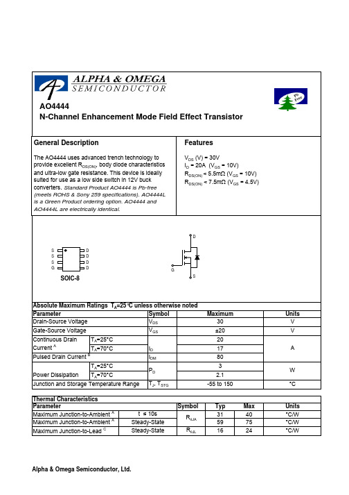
SymbolTyp Max 31405975R θJL 1624Maximum Junction-to-Ambient A Steady-State °C/W Maximum Junction-to-Lead CSteady-State°C/WThermal Characteristics ParameterUnits Maximum Junction-to-Ambient A t ≤ 10s R θJA °C/W AO4444AO4444SymbolMin TypMaxUnits BV DSS 30V 1T J =55°C5I GSS 100nA V GS(th)1 1.83V I D(ON)60A 3.9 5.5T J =125°C5.16.25.17.5m Ωg FS 106S V SD 0.721V I S4A C iss 32003840pF C oss 590pF C rss 414pF R g0.540.7ΩQ g (10V)6376nC Q g (4.5V)3340nC Q gs 8.6nC Q gd 17.6nC t D(on)12ns t r 15.5ns t D(off)40ns t f 14ns t rr 3441ns Q rr30nCTHIS PRODUCT HAS BEEN DESIGNED AND QUALIFIED FOR THE CONSUMER MARKET. APPLICATIONS OR USES AS CRITICAL COMPONENTS IN LIFE SUPPORT DEVICES OR SYSTEMS ARE NOT AUTHORIZED. AOS DOES NOT ASSUME ANY LIABILITY ARISING OUT OF SUCH APPLICATIONS OR USES OF ITS PRODUCTS. AOS RESERVES THE RIGHT TO IMPROVE PRODUCT DESIGN,FUNCTIONS AND RELIABILITY WITHOUT NOTICE.Body Diode Reverse Recovery Charge I F =20A, dI/dt=100A/µsGate Source Charge V GS =0V, V DS =15V, f=1MHz SWITCHING PARAMETERS Total Gate Charge Total Gate Charge Gate resistanceV GS =0V, V DS =0V, f=1MHzV GS =4.5V, V DS =15V, I D =20ATurn-On DelayTime Turn-On Rise Time Turn-Off DelayTime Gate Drain Charge Maximum Body-Diode Continuous CurrentInput Capacitance Output Capacitance DYNAMIC PARAMETERS m ΩV GS =4.5V, I D =15AI S =1A,V GS =0V V DS =5V, I D =20AR DS(ON)Static Drain-Source On-ResistanceForward TransconductanceDiode Forward Voltage I DSS µA Gate Threshold Voltage V DS =V GS I D =250µA V DS =24V, V GS =0VV DS =0V, V GS = ±20V Zero Gate Voltage Drain Current Gate-Body leakage current Electrical Characteristics (T J =25°C unless otherwise noted)STATIC PARAMETERS ParameterConditions Turn-Off Fall TimeBody Diode Reverse Recovery TimeI F =20A, dI/dt=100A/µsDrain-Source Breakdown Voltage On state drain currentI D =250µA, V GS =0V V GS =10V, V DS =5V V GS =10V, I D =20AReverse Transfer Capacitance V GS =10V, V DS =15V, R L =0.75Ω, R GEN =3ΩA: The value of R θJA is measured with the device mounted on 1in 2 FR-4 board with 2oz. Copper, in a still air environment with T A =25°C. The value in any given application depends on the user's specific board design. The current rating is based on the t ≤ 10s thermal resistance rating.B: Repetitive rating, pulse width limited by junction temperature.C. The R θJA is the sum of the thermal impedence from junction to lead R θJL and lead to ambient.D. The static characteristics in Figures 1 to 6 are obtained using 80 µs pulses, duty cycle 0.5% max.E. These tests are performed with the device mounted on 1 in 2FR-4 board with 2oz. Copper, in a still air environment with T A =25°C. The SOA curve provides a single pulse rating. Rev 1 : June 2005AO4444AO4444。
- 1、下载文档前请自行甄别文档内容的完整性,平台不提供额外的编辑、内容补充、找答案等附加服务。
- 2、"仅部分预览"的文档,不可在线预览部分如存在完整性等问题,可反馈申请退款(可完整预览的文档不适用该条件!)。
- 3、如文档侵犯您的权益,请联系客服反馈,我们会尽快为您处理(人工客服工作时间:9:00-18:30)。
Symbol
Typ Max 31405975R θJL 1624Maximum Junction-to-Ambient
A
Steady-State °C/W Maximum Junction-to-Lead
C
Steady-State
°C/W
Thermal Characteristics Parameter
Units Maximum Junction-to-Ambient A
t ≤ 10s R θJA °C/W AO4456
AO4456
Symbol
Min Typ
Max
Units BV DSS 30
V V DS =24V, V GS =0V
0.0080.1T J =125°C
9
20I GSS 0.1µA V GS(th)Gate Threshold Voltage 1.4 1.8
2.4
V I D(ON)120
A 3.8 4.6T J =125°C
5.97.44.5 5.6
m Ωg FS 112
S V SD
0.370.5V I S 5A C iss 6430
7716
pF C oss 756pF C rss 352pF
R g
0.9 1.4Ω
Q g (10V)96
115Q g (4.5V)4453
nC Q gs 17nC Q gd 13nC t D(on)17.5
ns t r 10ns t D(off)56ns t f 10.5ns
t rr 2025
ns Q rr
26
nC THIS PRODUCT HAS BEEN DESIGNED AND QUALIFIED FOR THE CONSUMER MARKET. APPLICATIONS OR USES AS CRITICAL COMPONENTS IN LIFE SUPPORT DEVICES OR SYSTEMS ARE NOT AUTHORIZED. AOS DOES NOT ASSUME ANY LIABILITY ARISING OUT OF SUCH APPLICATIONS OR USES OF ITS PRODUCTS. AOS RESERVES THE RIGHT TO IMPROVE PRODUCT DESIGN,FUNCTIONS AND RELIABILITY WITHOUT NOTICE.
Total Gate Charge VGS=10V, VDS=15V, ID=20A
Gate Drain Charge V GS =0V, V DS =15V, f=1MHz
SWITCHING PARAMETERS Total Gate Charge Gate Source Charge Gate resistance
V GS =0V, V DS =0V, f=1MHz
Turn-On Rise Time Turn-Off DelayTime V GS =10V, V DS =15V, R L =0.75Ω,
R GEN =3Ω
Turn-Off Fall Time
Turn-On DelayTime m ΩV GS =4.5V, I D =20A
I S =1A,V GS =0V V DS =5V, I D =20A Maximum Body-Diode + Schottky Continuous Current Input Capacitance Output Capacitance DYNAMIC PARAMETERS
R DS(ON)Static Drain-Source On-Resistance
Forward Transconductance
Diode Forward Voltage
V DS =V GS I D =250µA Electrical Characteristics (T J =25°C unless otherwise noted)STATIC PARAMETERS Parameter Conditions I DSS Zero Gate Voltage Drain Current mA V DS =0V, V GS = ±12V Gate-Body leakage current Body Diode Reverse Recovery Time Body Diode Reverse Recovery Charge
I F =20A, dI/dt=300A/µs
Drain-Source Breakdown Voltage On state drain current
I D =1mA, V GS =0V V GS =10V, V DS =5V V GS =10V, I D =20A
Reverse Transfer Capacitance I F =20A, dI/dt=300A/µs A: The value of R θJA is measured with the device in a still air environment with T A =25°C. The power dissipation P DSM and current rating I DSM are based on TJ(MAX)=150°C, using t ≤ 10s junction-to-ambient thermal resistance.B: Repetitive rating, pulse width limited by junction temperature TJ(MAX)=150°C.
C. The R θJA is the sum of the thermal impedence from junction to lead R qJL and lead to ambient.
D. The static characteristics in Figures 1 to 6 are obtained using <300 ms pulses, duty cycle 0.5% max.
E. These tests are performed with the device mounted on 1 in 2 FR-4 board with 2oz. Copper, in a still air environment with T A=25°C. The SOA curve provides a single pulse rating. Rev 1: June 2006
AO4456
AO4456
AO4456。
