TL6700AF260QJ;中文规格书,Datasheet资料
15C02MH-TL-E;中文规格书,Datasheet资料

1
2
(Top view)
SANYO : MCPH3
Parameter Collector-to-Base Voltage Collector-to-Emitter Voltage Emitter-to-Base Voltage Collector Current Collector Current (Pulse) Collector Dissipation Junction Temperature Storage Temperature
Switching Time Test Circuit
IB1 PW=20µs
D.C.≤1%
IB2
INPUT
VR
RB
50Ω +
220µF
VBE= --5V
IC=20IB1= --20IB2=400mA
OUTPUT
RL
+ 470µF
VCC=5V
Ratings
Unit
min
typ
max
20
V
15
V
5
V
30
Ron -- IB
10
f=1MHz
7
1kΩ IN
5
1kΩ
2
3
IT05041
OUT
3
IB
2
1.0 7 5
3 2
0.1 0.1
23
5 7 1.0
23
Base Current, IB -- mA
5 7 10 IT06664
Collector Dissipation, PC -- mW
100
7 1.0
700
Ta=7--52°5C°C
2
FFAF60UA60DN;中文规格书,Datasheet资料

PDP SPM™ Power-SPM™
PowerTrench® PowerXS™ Programmable Active Droop™ QFET® QS™ Quiet Series™ RapidConfigure™
™ Saving our world, 1mW/W/kW at a time™ SmartMax™ SMART START™ SPM® STEALTH™ SuperFET™ SuperSOT™-3 SuperSOT™-6 SuperSOT™-8 SupreMOS™ SyncFET™ Sync-Lock™
FFAF60UA60DN UItrafast Rectifier
FFAF60UA60DN UItrafast Rectifier
Features
• Ultrafast switching, Trr < 90ns • High Reverse Voltage and High Reliability • Avalanche Energy Rated • Max Forward Voltage, VF < 2.2V • RoHS Compliant
Avalanche Energy ( L = 40mH)
Notes: 1: Pulse: Test Pulse width = 300µs, Duty Cycle = 2%
TC = 25oC TC = 125oC TC = 25oC TC = 125oC
TC = 25oC
Min.
-
-
-
20
Test Circuit and Waveforms
™*
®
Fairchild® Fairchild Semiconductor® FACT Quiet Series™ FACT® FAST® FastvCore™ FETBench™ FlashWriter®*
ASM3P2811AF-08SR;ASM3P2811BF-08SR;ASM3P2812AF-08SR;ASM3P2812BF-08SR;中文规格书,Datasheet资料
ASM3P2811A/B and ASM3P2812A/B and ASM3P2814A/BLow Power EMI Reduction ICFeatures• FCC approved method of EMI attenuation• Provides up to 15dB EMI reduction• Generates a 1x, 2x and 4x low EMI spread spectrumclock of the input frequencyo1x: ASM3P2811A/Bo2x: ASM3P2812A/Bo4x: ASM3P2814A/B• Optimized for input frequency range from 10MHz to40MHz• Internal loop filter minimizes external componentsand board space• Selectable spread options:o Down Spread and Center Spread• 8 frequency deviation selections:o ±0.625% to -3.5%• Low inherent Cycle-to-Cycle Jitter• 3.3V Operating Voltage• CMOS/TTL compatible inputs and outputs.• Pin-out compatible with Cypress CY25811, CY25812and CY25814•Available in 8-pin SOIC and TSSOP PackagesProduct DescriptionThe ASM3P28XX devices are versatile spread spectrumfrequency modulators designed specifically for a widerange of input clock frequencies from 10MHz to 40MHz.Refer to Input/Output Frequency Range Selection Table.The ASM3P28XX can generate an EMI reduced clockfrom crystal, ceramic resonator, or system clock. TheASM3P28XX-A and the ASM3P28XX-B offer variouscombinations of spread options and percentagedeviations. Refer to Frequency Deviation and SpreadSelection Table. These combinations include Down andCenter Spread, and percentage deviation range from±0.625% to -3.5%.The ASM3P28XX reduces electromagnetic interference(EMI) at the clock source, allowing system wide reductionof EMI of downstream clock and data dependent signals.The ASM3P28XX allows significant system cost savingsby reducing the number of circuit board layers, ferritebeads, shielding, and other passive components that aretraditionally required to pass EMI regulations.The ASM3P28XX modulates the output of a single PLL inorder to “spread” the bandwidth of a synthesized clock,and more importantly, decreases the peak amplitudes ofits harmonics. This results in significantly lower systemEMI compared to the typical narrow band signal producedby oscillators and most frequency generators. LoweringEMI by increasing a signal’s bandwidth is called ‘spreadspectrum clock generation’.The ASM3P28XX uses the most efficient and optimizedmodulation profile approved by the FCC and isimplemented in a proprietary all-digital method.ApplicationsThe ASM3P28XX is targeted towards EMI managementfor memory and LVDS interfaces in mobile graphicchipsets and high-speed digital applications such as PCperipheral devices, consumer electronics, and embeddedcontroller systems.. Block DiagramPin ConfigurationPin DescriptionPin#Pin NameTypeDescription1 XIN / CLKINI Crystal connection or external Clock input. 2 VSS P Ground to entire chip.3 D_C I Digital logic input used to select Down (LOW) or Center (HIGH) spread options. (Refer to Frequency Deviation and Spread Selection Table ). This pin has an internal pull-up resistor.4 SRS I Spread range select. Digital logic input used to select frequency deviation (Refer to Frequency Deviation and Spread Selection Table ). This pin has an internal pull-up resistor.5 ModOUT O Spread spectrum clock output.6 FRS I Frequency range select. Digital logic input used to select Input frequency range (Refer to Input/Output Frequency Range Selection Table). This pin has an internal pull-up resistor.7 VDD P Power supply for the entire chip.8XOUTOCrystal connection. If using an external reference, this pin must be left unconnected.ModOUTFRSXOUT VDDInput/Output Frequency Range Selection TableFRS (pin 6)Part NumberModulation Rate ASM3P2811 (1x) ASM3P2812 (2x) ASM3P2814 (4x)Input(MHz)Output(MHz)Input(MHz)Output(MHz)Input(MHz)Output(MHz)0 10-20 10-20 10-20 20-40 10-20 40-80 Input Frequency / 4481 20-40 20-40 20-40 40-80 20-40 80-160 Input Frequency / 896 Output Frequency Deviation and Spread Selection TablePart NumberD_C(pin 3)SRS(pin 4)Frequency Deviation1 (%)FS=0 FS=110/20/40 (MHz) 20/40/80 (MHz) 20/40/80 (MHz) 40/80/160 (MHz)ASM3P28XXA 0 0 -3 -2.5 -2.7 -2.60 1 -3.7 -3.4 -3.8 -3.61 0 ±1.5 ±1.2 ±1.5 ±1.3 1 1 ±1.8 ±1.6 ±1.9 ±1.8ASM3P28XXB 0 0 -1.7 -1.0 -1.5 -1.40 1 -2.0 -1.5 -2.0 -1.91 0 ±0.75 ±0.6 ±0.8 ±0.7 1 1 ±1.0 ±0.75 ±1.0 ±0.9Note: 1. Frequency Deviation given in the table is for the Output Frequency Range covering ASM3P2811x / 12x / 14x.Absolute Maximum RatingsSymbol Parameter Rating Unit V DD, V IN Voltage on any pin with respect to Ground -0.5 to +4.6 V T STG Storage temperature -65 to +125 °C T s Max. Soldering Temperature (10 sec) 260 °C T J Junction Temperature 150 °C T DV Static Discharge Voltage(As per JEDEC STD 22- A114-B) 2 KV Note: These are stress ratings only and are not implied for functional use. Exposure to absolute maximum ratings for prolonged periods of time may affect device reliability..Operating ConditionsSymbol Parameter Min Max Unit VDD Supply Voltage 3.0 3.6 V T A Operating temperature -40 +85 °CC L Load Capacitance 10 pFC IN Input Capacitance 7 pFDC Electrical CharacteristicsSymbol Parameter Min Typ Max Unit V IL Input low voltage VSS – 0.3 0.8 V V IH Input high voltage 2 V DD + 0.3 VI IL Input low current(Inputs D_C, SRS and FRS are pulled high internally) -50 µAI IH Input high current 50 µAI XOL XOUT Output low current(V XOL@ 0.4V, V DD = 3.3V) 3 mAI XOH XOUT Output high current(V XOH@ 2.5V, V DD = 3.3V) 3 mA V OL Output low voltage (V DD = 3.3V, I OL = 5mA) 0.4 V V OH Output high voltage (V DD = 3.3V, I OH = -5mA) 2.5 VI CC Dynamic supply current (Unloaded Output) 8 18 mAI DD Static supply current , Standby mode(CLKIN pulled to GND) 4.5 mA VDD Operating voltage 3.0 3.3 3.6 V t ON Power up time (first locked clock cycle after power up) 500 µS Z OUT Clock out impedance 76 ΩAC Electrical CharacteristicsSymbol Parameter Min Typ Max Unitf IN Input frequency for ASM3P2811/12/13/14 A/B 10 40 MHzf OUT Output frequency for ASM3P2811A/B 10 40 MHz Output frequency for ASM3P2812A/B 20 80 MHz Output frequency for ASM3P2814A/B 40 160 MHzt LH1Output rise time (measured at 0.8V to 2.0V) 0.5 0.9 1.2 nS t HL1Output fall time (measured at 2.0V to 0.8V) 0.8 1.0 1.3 nS t JC Cycle-to-Cycle Jitter (Unloaded Output) ±250 pS t D Output duty cycle 45 50 55 % Note: 1. t LH and t HL are measured into a capacitive load of 10pF.. Package Information8-Pin SOIC PackageDEHDA 1A 2AθLCBeSymbolDimensionsInches MillimetersMinMaxMin MaxA1 0.004 0.010 0.10 0.25 A 0.053 0.069 1.35 1.75 A2 0.049 0.059 1.25 1.50 B 0.012 0.020 0.31 0.51 C 0.0070.0100.180.25D 0.193 BSC 4.90 BSCE 0.154 BSC 3.91 BSC e 0.050 BSC 1.27 BSC H 0.236 BSC 6.00 BSC L 0.016 0.050 0.41 1.27 θ0°8°0°8° Note: Controlling dimensions are millimeters.SOIC: 0.074 grams unit weight.. EHAA1A2DBCLθe 8-lead TSSOP (4.40-MM Body)SymbolDimensionsInchesMillimeters MinMaxMinMaxA 0.043 1.10 A1 0.002 0.006 0.05 0.15 A2 0.033 0.037 0.85 0.95B 0.008 0.012 0.19 0.30 c 0.004 0.008 0.09 0.20 D 0.114 0.122 2.90 3.10 E 0.1690.1774.304.50e 0.026 BSC 0.65 BSC H 0.252 BSC6.40 BSCL 0.020 0.028 0.50 0.70 θ 0° 8° 0° 8°Ordering CodePart Number Marking Package Type TemperatureASM3P2811AF-08SR ACH 8-Pin SOIC, Tape & Reel, Pb free 0°C to 70°CASM3P2811BF-08SR ACJ 8-Pin SOIC, Tape & Reel, Pb free 0°C to 70°CASM3P2812AF-08SR ACL 8-Pin SOIC, Tape & Reel, Pb free 0°C to 70°CASM3P2812AF-08TR ACL 8-Pin TSSOP, Tape & Reel, Pb free 0°C to 70°CASM3P2812BF-08SR ACN 8-Pin SOIC, Tape & Reel, Pb free 0°C to 70°CASM3P2814AF-08SR ACP 8-Pin SOIC, Tape & Reel, Pb free 0°C to 70°CASM3P2814BF-08TR ACR 8-Pin TSSOP, Tape & Reel, Pb free 0°C to 70°CA “microdot” placed at the end of last row of marking or just below the last row toward the center of package indicates Pb-freeON Semiconductor and are registered trademarks of Semiconductor Components Industries, LLC (SCILLC). SCILLC reserves the right to make changes without further notice to any products herein. SCILLC makes no warranty, representation or guarantee regarding the suitability of its products for any particular purpose, nor does SCILLC assume any liability arising out of the application or use of any product or circuit, and specifically disclaims any and all liability, including without limitation special, consequential or incidental damages. “Typical” parameters which may be provided in SCILLC data sheets and/or specifications can and do vary in different applications and actual performance may vary over time. All operating parameters, including “Typicals” must be validated for each customer application by customer's technical experts. SCILLC does not convey any license under its patent rights nor the rights of others.SCILLC products are not designed, intended, or authorized for use as components in systems intended for surgical implant into the body, or other applications intended to support or sustain life, or for any other application in which the failure of the SCILLC product could create a situation where personal injury or death may occur. Should Buyer purchase or use SCILLC products for any such unintended or unauthorized application, Buyer shall indemnify and hold SCILLC and its officers, employees, subsidiaries, affiliates, and distributors harmless against all claims, costs, damages, and expenses, and reasonable attorney fees arising out of, directly or indirectly, any claim of personal injury or death associated with such unintended or unauthorized use, even if such claim alleges that SCILLC was negligent regarding the design or manufacture of the part. SCILLC is an Equal Opportunity/Affirmative Action Employer. U.S Patent Pending; Timing-Safe and Active Bead are trademarks of PulseCore Semiconductor, a wholly owned subsidiary of ON Semiconductor. This literature is subject to all applicable copyright laws and is not for resale in any manner.PUBLICATION ORDERING INFORMATIONLITERATURE FULFILLMENT:Literature Distribution Center for ON Semiconductor P.O. Box 5163, Denver, Colorado 80217 USA Phone: 303-675-2175 or 800-344-3860 Toll Free USA/CanadaFax: 303-675-2176 or 800-344-3867 Toll Free USA/CanadaEmail: orderlit@ N. American Technical Support: 800-282-9855Toll Free USA/CanadaEurope, Middle East and Africa TechnicalSupport:Phone: 421 33 790 2910Japan Customer Focus CenterPhone: 81-3-5773-3850ON Semiconductor Website:Order Literature: /orderlitFor additional information, please contact yourlocal Sales Representative.分销商库存信息:ONSEMIASM3P2811AF-08SR ASM3P2811BF-08SR ASM3P2812AF-08SR ASM3P2812BF-08SR ASM3P2812AF-08TR ASM3P2814AF-08SR ASM3P2814BF-08TR。
TCST2103;中文规格书,Datasheet资料
Transmissive Optical Sensor with Phototransistor OutputTCST2103, TCST2202, TCST2300Vishay SemiconductorsDESCRIPTIONThe TCST2103, TCST2202, and TCST2300 are transmissive sensors that include an infrared emitter and phototransistor, located face-to-face on the optical axes in a leaded package which blocks visible light. These part numbers include options for aperture width.FEATURES•Package type: leaded •Detector type: phototransistor•Dimensions (L x W x H in mm): 24.5 x 6.3 x 10.8•Gap (in mm): 3.1•Typical output current under test: C = 4 mA (TCST2103)•Typical output current under test: I C = 2 mA (TCST2202)•Typical output current under test: I C = 0.5 mA (TCST2300)•Daylight blocking filter •Emitter wavelength: 950 nm •Lead (Pb)-free soldering released•Compliant to RoHS directive 2002/95/EC and in accordance to WEEE 2002/96/ECAPPLICATIONS•Optical switch •Photo interrupter •Counter •EncoderNote(1)Conditions like in table basic characteristics/couplerNote(1)MOQ: minimum order quantity19180_4PRODUCT SUMMARYPART NUMBER GAP WIDTH(mm)APERTURE WIDTH(mm)TYPICAL OUTPUT CURRENTUNDER TEST (1)(mA)DAYLIGHTBLOCKING FILTER INTEGRATEDTCST2103 3.114Yes TCST2202 3.10.52Yes TCST23003.10.250.5YesORDERING INFORMATIONORDERING CODE PACKAGINGVOLUME (1)REMARKS TCST2103Tube MOQ: 1020 pcs, 85 pcs/tube With mounting flange TCST2202Tube MOQ: 1020 pcs, 85 pcs/tube With mounting flange TCST2300TubeMOQ: 1020 pcs, 85 pcs/tubeWith mounting flangeABSOLUTE MAXIMUM RATINGS (1)PARAMETER TEST CONDITIONSYMBOLVALUEUNITCOUPLERTotal power dissipation T amb ≤ 25 °CP tot 250mW Ambient temperature range T amb - 55 to + 85°C Storage temperature range T stg - 55 to + 100°C Soldering temperatureDistance to package: 2 mm; t ≤ 5 sT sd260°CTCST2103, TCST2202, TCST2300Vishay SemiconductorsTransmissive Optical Sensor withPhototransistor OutputNote (1)T amb = 25 °C, unless otherwise specifiedABSOLUTE MAXIMUM RATINGSFig. 1 - Power Dissipation Limit vs. Ambient TemperatureINPUT (EMITTER)Reverse voltage V R 6V Forward current I F 60mA Forward surge current t p ≤ 10 µs I FSM 3A Power dissipation T amb ≤ 25 °CP V 100mW Junction temperature T j100°COUTPUT (DETECTOR)Collector emitter voltage V CEO 70V Emitter collector voltage V ECO 7V Collector peak current t p /T = 0.5, t p≤ 10 msI CM 200mA Power dissipation T amb ≤ 25 °CP V 150mW Junction temperatureT j100°CABSOLUTE MAXIMUM RATINGS (1)PARAMETER TEST CONDITIONSYMBOLVALUEUNITBASIC CHARACTERISTICS (1)PARAMETER TEST CONDITIONPARTSYMBOLMIN.TYP.MAX.UNITCOUPLERCurrent transfer ratioV CE = 5 V, I F = 20 mATCST2103CTR 1020%TCST2202CTR 510%TCST2300CTR 1.25 2.5%Collector currentV CE = 5 V, I F = 20 mA TCST2103I C 24mA TCST2202I C 12mA TCST2300I C 0.250.5mA Collector emitter saturationvoltageI F = 20 mA, I C = 1 mA TCST2103V CEsat 0.4V I F = 20 mA, I C = 0.5 mA TCST2202V CEsat 0.4V I F = 20 mA, I C = 0.1 mA TCST2300V CEsat 0.4V Resolution, path of the shutter crossing the radiant sensitive zoneI Crel = 10 % to 90 %TCST2103s 0.6mm TCST2202s 0.4mm TCST2300s0.2mmTCST2103, TCST2202, TCST2300T ransmissive Optical Sensor withPhototransistor OutputVishay SemiconductorsNote (1)T amb = 25 °C, unless otherwise specifiedFig. 2 - Test Circuit for t on and t offFig. 3 - Switching TimesBASIC CHARACTERISTICST amb = 25°C, unless otherwise specifiedFig. 4 - Forward Current vs. Forward Voltage Fig. 5 - Relative Current Transfer Ratio vs. Ambient TemperatureINPUT (EMITTER)Forward voltage I F = 60 mA V F 1.25 1.6V Junction capacitance V R = 0 V, f = 1 MHzC j50pFOUTPUT (DETECTOR)Collector emitter voltage I C = 1 mA V CEO 70V Emitter collector voltage I E = 10 µAV ECO 7V Collector dark currentV CE = 25 V, I F = 0 A, E = 0 lxI CEO100nASWITCHING CHARACTERISTICS Turn-on time I C = 2 mA, V S = 5 V,R L = 100 Ω (see figure 2)t on 10µs Turn-off timeI C = 2 mA, V S = 5 V,R L = 100 Ω (see figure 2)t off8µsBASIC CHARACTERISTICS (1)PARAMETER TEST CONDITIONPARTSYMBOLMIN.TYP.MAX.UNIT10 %90 %100 %I FI C t p P u lse d u ration t d Delay time t rRise time t on (= t d + t r ) T u rn-on timet s Storage time t fFall time t off (= t s + t f )T u rn-off time96 11698TCST2103, TCST2202, TCST2300Vishay Semiconductors Transmissive Optical Sensor withPhototransistor OutputFig. 6 - Collector Dark Current vs. Ambient Temperature Fig. 7 - Collector Current vs. Forward Current Fig. 8 - Collector Current vs. Collector Emitter VoltageFig. 9 - Current Transfer Ratio vs. Forward Current Fig. 10 - Turn-off/Turn-on Time vs. Collector Current Fig. 11 - Relative Collector Current vs. DisplacementTCST2103, TCST2202, TCST2300T ransmissive Optical Sensor withPhototransistor OutputVishay SemiconductorsFig. 12 - Relative Collector Current vs. Displacement Fig. 13 - Relative Collector Current vs. DisplacementPACKAGE DIMENSIONS in millimetersTCST2103, TCST2202, TCST2300Vishay Semiconductors Transmissive Optical Sensor withPhototransistor Output TUBE DIMENSIONS in millimetersPackaging and Ordering InformationPackaging and Ordering InformationVishay SemiconductorsNotes(1)MOQ: minimum order quantity (2)Please refer to datasheetsTUBE SPECIFICATION FIGURESFig. 1PART NUMBER MOQ (1)PCS PER TUBETUBE SPEC.(FIGURE)CONSTITUENTS(FORMS)CNY70400080128TCPT1300X012000Reel (2)29TCRT10001000Bulk -26TCRT10101000Bulk -26TCRT5000450050227TCRT5000L 240048327TCST1030520065524TCST1030L 260065624TCST1103102085424TCST1202102085424TCST1230480060724TCST1300102085424TCST2103102085424TCST2202102085424TCST2300102085424TCST5250486030824TCUT1300X012000Reel (2)29TCZT8020-PAER2500Bulk-22Packaging and Ordering InformationVishay Semiconductors Packaging and Ordering InformationFig. 2Fig. 3Packaging and Ordering Information Packaging and Ordering Information Vishay SemiconductorsFig. 4Fig. 5Packaging and Ordering InformationVishay Semiconductors Packaging and Ordering InformationFig. 6Fig. 7分销商库存信息: VISHAYTCST2103。
slf系列贴片电感datasheet
特点 ●是最适用于电源系统的低直流电阻,大电流,节能型产品。 ●因采用磁力屏蔽结构,所以可实现高密度安装。 ●底面为平直的低背型 , 可稳定地安装在电路板上。 ●采用卷带仕样,支持自动插入机。 用途 手机,计算机,硬盘驱动器,其他各种电子设备 仕样
工作温度范围 保存温度范围 –20 to +85°C [包括自身温度上升] –40 to +85°C [产品单体]
电气特性
电感 (H) 4.7 6.8 10 15 22 33 47 68 100 150 220 电感容差 ±20% ±20% ±20% ±20% ±20% ±20% ±20% ±20% ±20% ±20% ±20% L 测定频率 (kHz) 100 100 100 100 100 100 100 100 100 100 100 直流电阻 ( )±20% 0.0284 0.0354 0.0532 0.0745 0.104 0.148 0.21 0.29 0.43 0.65 0.98 额定电流 (A) 基于电感 变化率时 1.6max. 1.5max. 1.3max. 1max. 0.77max. 0.69max. 0.59max. 0.5max. 0.42max. 0.34max. 0.26max. 基于温度 上升时 2.5typ. 2.2typ. 1.8typ. 1.4typ. 1.3typ. 1.1typ. 0.92typ. 0.78typ. 0.64typ. 0.5typ. 0.38typ. 品名 SLF6028T-4R7M1R6-PF SLF6028T-6R8M1R5-PF SLF6028T-100M1R3-PF SLF6028T-150M1R0-PF SLF6028T-220MR77-PF SLF6028T-330MR69-PF SLF6028T-470MR59-PF SLF6028T-680MR50-PF SLF6028T-101MR42-PF SLF6028T-151MR34-PF SLF6028T-221MR26-PF
MX23A34SF1;MX23A26SF1;MX23A36SF1;MX23A18SF1;MX23A12SF1;中文规格书,Datasheet资料

•Insulation resistance: 100M ohm min. •Life time: 50 times •Applicable wire : Position of using wire is specified. Cable type Conductive area A.W.G No. Sheath diameter AVSS, AVS(partially) 0.3 to 1.25mm2 #22 to #16 1.6dia. to 2.2dia. mm
Part Number MX23A12SF1 MX23A12XF1 MX23A12NF1 MX23A18SF1 MX23A18XF1 MX23A18NF1 MX23A18NF2 MX23A26SF1 MX23A26XF1 MX23A26NF1 MX23A26NF2 MX23A34SF1 MX23A34XF1 MX23A34NF1 MX23A34NF2 M23S05K351 M120-55780
■Socket Contact Materials/Finishes Copper alloy/Sn plating
Rear cover Grommet Socket housing
Seal ring Front cap
Pin insulator
Pin contact
Crimp tool
Hand crimping tool CT160-3B-MX23 Semi automatic applicator 350-MX23-2 Contact release jig ET-MX23
mx23a34sf1;mx23a26sf1;mx23a36sf1;mx23a18sf1;mx23a12sf1;中文规格书,datasheet资料 componentsproduct information connector new 1/7 mb-0094-2 june 2006 jae pmk div. proprietary. copyright 2006,japanaviation electronics industry, ltd. features general specifications mx23a series compact type low-profiled waterproof connector contacts:12 ,18, 26, 34 pos. (pin side 2types: reverse standard**excluding 12 pos.) contact resistance: 10m ohm max.?dielectric withstanding voltage: ac 1000 vr.m.s minute)?operating temperature: -40 to+125 deg. (includingtemperature rise caused powerdistribution)?current rating: 3a?insulation resistance: 100m ohm min.?life time: 50 times?applicable wire usingwire specified.low profiled type boardmounting height socketconnector height 22.2mmmax. double fin structure highreliability socketcontact largechamfer front-edgeside preventgrommet from damaging. incomplete insertion socketcontact itshousing can frontcap mounting process. full water poof grommet socketcontact crimping area reducesize. water pro
薄型模块式电源系统 N6700 系列用户指南说明书
用户指南Keysight Technologies 薄型模块式电源系统N6700系列法律声明© Keysight Technologies 2006 - 2014根据美国和国际版权法,未经Keysight Technologies 事先同意和书面许可,本文档的任何部分不得影印、复制或翻译成其他语言。
担保本文档中包含的材料“按原样”提供,如有更改,恕不另行通知。
此外,在适用法律所允许的最大范围内,Keysight 对与此手册相关的内容及其中所含的信息不作任何明示或默示的保证,包括但不限于对适销性和适用于特定目的所作的默示保证。
Keysight 对与提供、使用本手册及其所含信息以及与执行手册中的步骤有关的任何错误或偶然及继发性损坏不承担任何责任。
如果Keysight 与用户之间单独签定的协议中的保证条款涉及本文档中的内容,并且与本文档中的条款相抵触,则应以单独协议中的保证条款为准。
手册版本手册部件号:5969-2937CH第8版,2014年11月马来西亚印刷。
本手册的重印版包含少量更正和更新,可能具有相同的印刷日期。
修订版则标有新的印刷日期。
遵从有关标准的声明本产品和其他Keysight 产品的“遵从有关标准的声明”可以从Web 中下载。
请访问/go/conformity,然后单击“Declarations of Conformity”。
然后,您可以按产品编号进行搜索,找到最新的“遵从有关标准的声明”废弃电子电气设备 (WEEE) 指令2002/96/EC本产品符合 WEEE 指令 (2002/96/EC) 市场营销要求。
贴附于产品上的标签(请见下方)指示,不得将本电子/电气产品随同家庭废弃物一起处理。
产品类别:根据WEEE 指令Annex 1中的设备类型分类,此产品被归类为“监测和控制仪器”产品。
请勿作为家庭废弃物处理。
要退回不需要的产品,请与当地的Keysight 办事处联系,或访问/environment/product以了解详细信息。
CG2145MS,CG2800MS,CG75MS,CG75LTR,CG2800LTR,CG2600LTR,CG2470L,CG75L, 规格书,Datasheet 资料

CG/CG2 Series
CG/CG2 Series
Description
Littelfuse highly reliable CG/CG2 Series GDTs provide a high degree of surge protection in a small size ideal for board level circuit protection. GDTs function as switches which dissipate a minimum amount of energy and therefore handle currents that far surpass other types of transient voltage protection. Their gas-filled, rugged ceramic metal construction make them well suited to adverse environments. The CG/CG2 series comes in a variety of forms including surface mount, core, straight and shaped leads, to serve a variety of mounting methods.
AGENCY FILE NUMBER
Agency Approvals
AGENCY
& &
2 Electrode GDT Graphical Symbol
The CG Series (75-110V) is ideal for protection of test and communication equipment and other devices in which low voltage limits and extremely low arc voltages are required. The CG2 Series (145V-1000V) is ideal for protecting equipment where higher voltage limits and holdover voltages are necessary.
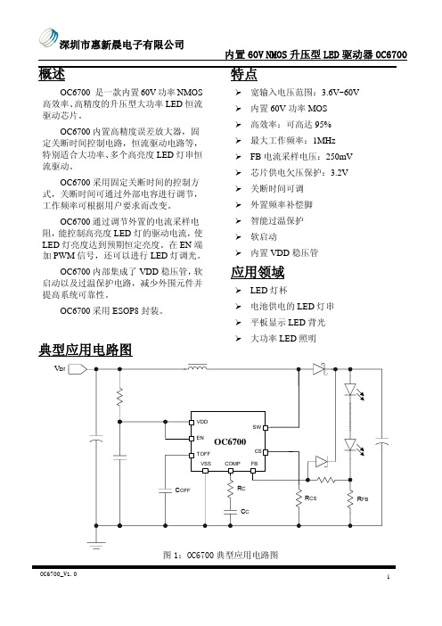
OC6700规格书2017年新版
静电耐压值(人体模型)
最大值 60 5.5
VDD+0.3 0.8 125 85 125 240 2000
单位 V V
V W oC
PP
oC
PP
oC
PP
oC
PP
V
注 1:超过上表中规定的极限参数会导致器件永久性损坏,而工作在以上极限条件下可能会影响器件的可靠性。
OC6700_V1.0
4
深圳市 惠新晨电子有限公 司
芯片通过 CS 管脚采样电感电流,实现峰值电流控制。此外,CS 脚还用来限制最大输入 电流,实现过流保护功能。
系统关断时间可通过连接到TOFF管脚的电容COFF来设置。通过设定关断时间,可设置系 统的工作频率。
COMP 管脚是误差放大器的输出端,可以在 COMP 脚外接电阻、电容来实现频率补偿。
OC6700 内部集成了 VDD 稳压管,以及软启动和过温保护电路。
深圳市 惠新晨电子有限公 司
概述
OC6700 是一款内置 60V 功率 NMOS 高效率、高精度的升压型大功率 LED 恒流 驱动芯片。
OC6700 内置高精度误差放大器,固 定关断时间控制电路,恒流驱动电路等, 特别适合大功率、多个高亮度 LED 灯串恒 流驱动。
OC6700 采用固定关断时间的控制方 式,关断时间可通过外部电容进行调节, 工作频率可根据用户要求而改变。
内置 60V NMOS 升压型 LED 驱动器 OC6700
管脚描述
管脚号 1 2 3 4 5 6 7 8
管脚名 GND EN COMP FB SW CS TOFF VDD
管脚类型 地 输入 输出 输入 输出 输入 输入 电源
描述 接地 芯片使能端,高电平有效 频率补偿脚 输出电流检测反馈脚 功率管漏极 输入限流检测脚 关断时间设置 芯片电源
F960中英文规格书

Product pictures:产品图片批准/日期深圳市永興輝實業發展有限公司Shenzhen YXH Industry Development Co.,Ltd编号:YXH-SPE-CE-3008版本:00/00日期:2009-7-03F960产品规格书地址:广东省深圳市龙岗区中心城五联社区连心路五联工业区桑格电子电话:0755-********Customer Approval:客户承认SpecificationProduct model:F960产品型号:F960Customer Model:客户型号:传真:0755-********编制/日期审核/日期F960锂离子电池规格说明书F960 Li-ion Battery specification1.范围 Range1.1 这份说明书适用于可充电的F960锂离子电池. This specification apply to rechargeable li-ion battery F9601.2 这份说明书仅适用于F960的电池 This specification only fit for F960 Battery2.种类型号 Type&model2.1 种类 Type锂离子可充电电池 Li-ion Rechargeable battery2.2 型号 modelSG-DVBT008-F960为公司型号 SG-DVBT008-F960 Company model3.规格 specification3.1 电芯18650规格 Battery Cell 18650 Specification数值C riteria 单位Units 单位U nits 数值C riteria单位Units单位U nits4.325-4.375伏(V)微安(uA)4.10-4.20伏(V)毫欧(m Ω)2.2-2.4伏(V)安(A)0.3-0.5毫秒(mS)KW76AABU1U211-153.2.7过流保护电流Over-currentprotection current数值C riteria 电性能参数 electrical property parameter项目Item 50-653.2.6内阻Conduction resistance 3.2.5自耗电流 self-consuming current项目I tem项目Item数值C riteria29-403.2.2过充恢复电压Over-chargeresuming voltage 3.2.3过放保护电压Over-discharge protection Voltage 3.2.8识别电阻(T) 识别电阻(D)锂电保护IC开关MOS管8205(SOP8)Picture and dimension3.3 F960 外壳规格 F960 Specification of shell3.1.14 外表标示 apperance marking ICR 18650目视 visual3.2.4短路保护延时间Short circuit protection delay外型尺寸3.2 F960 PCB板的规格 F960 PCB SpecificationMain chip application3.2.1过充保护电压Over-chargeProtection Voltage ItemTesting condition项目I tem 备注:1C=2100mAhThickness:1.9mm正负公差:0.1mm标 准 standard测试条件 Test condition3.4.1 标称电压 nominal voltage 6450mAh3.3.1 面3.4 F960成品规格 F960 finished-product Specification高精度数显卡尺high-precision callipers3.3.3 组合高精度数显卡尺high-precision callipers内阻仪 BVIR ≥6300mAh 典型6450mAhtypical 6450mAh高精度数显卡尺high-precision callipers 3.3.2 底5.5V 7.8V±0.1V ﹤86m Ω规 格 Specification 项目 item8.5V 3.4.7 出厂内阻 routine internal resistance 3.4.8 重量 weight3.4.9 外尺寸 outside dimension293g70.4*38.5*59.7mm分容老化柜 grading andaging cabinet 高精度万用表high precision digitalmultimeter天秤 Libra 3.4.6 出厂电压 routine voltage 7.2V3.4.2 标称容量 nominal capacity 高精度数显卡尺high-precision callipers3.4.3 实际容量 practical capacity 3.4.4 充电终止电压 final charging voltage3.4.5 放电终止电压final discharging voltage正负公差:0.1mm正负公差:0.1mm长宽公差:±0.1mm 厚度公差:±0.05mm4. 电池船运条件及保质期限 The shipping conditions and warranty4.1 船运条件:大约20-30%容量.4.2 保质期限:从电池生产完成日开始的12个月内.5. 电池使用时警告及注意事项:WARNINGS AND CAUTIONS IN HANDING THE LITHIUM-IONBATTERY警告warningA、危险警告: Danger warningDanger warning should be described in manual or instruction for users为防止电池可能发生泄漏,发热,爆炸,请注意以下预防措施:To prevent the possibility of the battery from leaking,heating, explosion please observe the following precautions:with metal objects such wirehairpins etcB、注意以下项目* 不要加热和扔进火中.Do not heat or expose charger to fire.* 禁止拆开电池及改变电池内部结构Do not open the battery and change the internal structure* 不要装配或遗留在高温(超过60℃)设备中.Do not assemble or leave it in the hightemperature equipment (≥60℃)* 不要用金属直接短接电池正极和负极终端.Do not use metal directly contacting battery positive and negative poles* 不要湿水,受潮.Keep away from water ; Dampproof充电注意chargering attention* 充电温度限制在 0℃至 +45℃.chargering temperature limited between 0℃ and +45℃.* 不要反充和未充电就进行过放电.Do not over discharge before* 最好的充电是按电池专门设计方式进行.The best charging way is according the battery special designed way* 充电时用制造厂指定的设备并遵循正确使用方法;When charging,using the appointed machine of factory and following thecorrect using way.放电注意Dischargering Attention* 放电温度限制在-20℃至 +60℃.discharging temperature limited between 20℃ and +60℃* 避免放电至2.5V以下, 不要过放电至1.0V以下.Avoid discharging below 2.5V,do not over discharger below1.0 V* 以规格书指定的电流放电并遵循环境温度.Following as specification appointed current dischargeand environmental temperature贮存注意Storage Attention* 贮存一个较长时期后要完全充放不少于三个循环.After storing for a long time,need fully charge anddischarge not less than three cycles.* 贮存在干燥和室温条件.Store at the dry and indoor condition* 贮存时电池带电量不多于30%.The battery with quantity ofelectricity less than 30% when storing.C、小心Carefulness引起电池过热,起火或功能失效,寿命减短。
ASM3P2474AF-06OR;中文规格书,Datasheet资料
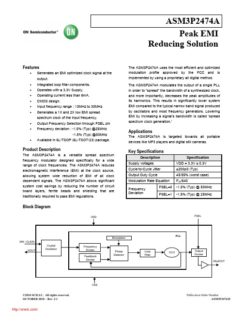
ASM3P2474APeak EMIReducing SolutionFeatures•Generates an EMI optimized clock signal at theoutput.•Integrated loop filter components.•Operates with a 3.3V Supply.•Operating current less than 6mA.•CMOS design.•Input frequency range : 13MHz to 30MHz•Generates a 1X and 2X low EMI spreadspectrum clock of the input frequency.•Output Frequency Selection through FSEL pin•Frequency deviation : -1.5% (Typ) @25MHz-1.5% (Typ) @50MHz•Available in 6L-TSOP (6L-TSOT-23) package.Product DescriptionThe ASM3P2474A is a versatile spread spectrumfrequency modulator designed specifically for a widerange of clock frequencies. The ASM3P2474A reduceselectromagnetic interference (EMI) at the clock source,allowing system wide reduction of EMI of all clockdependent signals. The ASM3P2474A allows significantsystem cost savings by reducing the number of circuitboard layers, ferrite beads and shielding that aretraditionally required to pass EMI regulations.The ASM3P2474A uses the most efficient and optimizedmodulation profile approved by the FCC and isimplemented by using a proprietary all digital method.The ASM3P2474A modulates the output of a single PLLin order to “spread” the bandwidth of a synthesized clock,and more importantly, decreases the peak amplitudes ofits harmonics. This results in significantly lower systemEMI compared to the typical narrow band signal producedby oscillators and most frequency generators. LoweringEMI by increasing a signal’s bandwidth is called ‘spreadspectrum clock generation.’ApplicationsThe ASM3P2474A is targeted towards all portabledevices like MP3 players and digital still cameras.Key SpecificationsDescription SpecificationSupply voltages VDD = 3.3V ± 0.3VCycle-to-Cycle Jitter±200pS (Typ)Output Duty Cycle45/55% (worst case)Modulation Rate Equation FIN/640FrequencyDeviationFSEL=0-1.5% (Typ) @ 50MHzFSEL=1-1.5% (Typ) @ 25MHz Block DiagramModOUTVDDVSSPin Configuration (6L-TSOP Package)Pin DescriptionPin# Pin Name Type Description1 FSEL I Selection Pin for 1X and 2X Output Frequency Options. Please refer to the table Frequency Selection Options for further details.2 XOUT O Crystal connection. If using an external reference, this pin must be left unconnected.3 XIN / CLKINI Crystal connection or external reference frequency input. This pin has dual functions. It can be connected either to an external crystal or an external reference clock. 4 VDD P Power supply for the entire chip. 5 ModOUT O Spread spectrum clock output. 6 VSSPGround connection.Modulation ProfileSpecificationsDescription Specification Frequency Range 13MHz < CLKIN < 30MHzModulation Equation F IN /640Frequency DeviationFSEL=0 -1.5% (Typ) @ 50MHz FSEL=1-1.5% (Typ) @ 25MHzFrequency Selection OptionsFSEL PinInput Frequency (MHz)Output Frequency (MHz)13-3026-60113-30 13-30Absolute Maximum RatingsSymbol Parameter Rating Unit VDD, V IN Voltage on any pin with respect to Ground-0.5 to +4.6V T STG Storage temperature-65 to +125°C T s Max. Soldering Temperature (10 sec)260°C T J Junction Temperature150°C2KV T DV Static Discharge Voltage(As per JEDEC STD22- A114-B)Note: These are stress ratings only and are not implied for functional use. Exposure to absolute maximum ratings for prolonged periods of time may affect device reliability.Operating ConditionsParameter Description Min Max Unit VDD Supply Voltage 3 3.6 V T A Operating Temperature (Ambient Temperature) 0 70 °CC L Load Capacitance 15 pFC IN Input Capacitance 7 pF DC Electrical CharacteristicsSymbol Parameter Min Typ Max Unit V IL Input low voltage VSS-0.30.8V V IH Input high voltage 2.0VDD+0.3VI IL Input low current -35µAI IH Input high current35µAI XOL XOUT output low current (@ 0.4V, VDD = 3.3V)3mAI XOH XOUT output high current (@ 2.5V, VDD = 3.3V)3mAV OL Output low voltage (VDD = 3.3V, I OL = 8mA)0.4V V OH Output high voltage (VDD = 3.3V, I OH = 8mA) 2.5VI DD Static supply current1 1.6mAI CC Dynamic supply current(3.3V, 25MHz and no load and FSEL=1) 4.0mAVDD Operating voltage 3.0 3.3 3.6V t ON Power-up time (first locked cycle after power-up)5mS Z OUT Output impedance45ΩNote: 1. XIN /CLKIN pin is pulled low.AC Electrical CharacteristicsSymbol ParameterMin Typ Max Unit CLKIN Input frequency 13 30 MHz ModOUTOutput frequency FSEL = 0 26 60 MHz FSEL = 113 30 f d Frequency Deviation Output Frequency = 13MHz -1.8 %Output Frequency = 30MHz -0.9 f d Frequency DeviationOutput Frequency = 26MHz -1.8 % Output Frequency = 60MHz-0.9 t LH 1Output rise time (measured from 0.8 to 2.0V) 0.4 0.85 1.1 nS t HL 1 Output fall time (measured at 2.0V to 0.8V) 0.3 0.7 0.9 nS t JC Jitter (cycle-to-cycle) ±200 pS t DOutput duty cycle455055%Note: 1. t LH and t HL are measured into a capacitive load of 15pF.Typical Crystal SpecificationsFundamental AT cut parallel resonant crystalNominal frequency 25MHzFrequency tolerance ± 30 ppm or better at 25°C Operating temperature range -25°C to +85°C Storage temperature -40°C to +85°C Load capacitance(C P ) 18pFShunt capacitance 7pF maximum ESR25 ΩNote: Note: C L is Load Capacitance and Rx is used to prevent oscillations at overtone frequency of the Fundamental frequency.Typical Crystal Interface CircuitC L = 2*(C P – C S ),Where C P = Load capacitance of crystalC S = Stray capacitance due to C IN, PCB, Trace etc.Typical Application SchematicModOUT ClockPackage Information6L-TSOP PackageSymbolDimensionsInches Millimeters Min Max Min MaxA 0.04 1.00 A1 0.00 0.004 0.00 0.10 A2 0.033 0.036 0.84 0.90 b 0.012 0.02 0.30 0.50 H 0.005 BSC 0.127 BSCD 0.114 BSC 2.90 BSCB 0.06 BSC 1.60 BSCe 0.0374 BSC 0.950 BSCC 0.11 BSC 2.80 BSCL 0.0118 0.02 0.30 0.50 θ0°4°0°4°ON Semiconductor and are registered trademarks of Semiconductor Components Industries, LLC (SCILLC). SCILLC reserves the right to make changes without further notice to any products herein. SCILLC makes no warranty, representation or guarantee regarding the suitability of its products for any particular purpose, nor does SCILLC assume any liability arising out of the application or use of any product or circuit, and specifically disclaims any and all liability, including without limitation special, consequential or incidental damages. “Typical” parameters which may be provided in SCILLC data sheets and/or specifications can and do vary in different applications and actual performance may vary over time. All operating parameters, including “Typicals” must be validated for each customer application by customer's technical experts. SCILLC does not convey any license under its patent rights nor the rights of others. SCILLC products are not designed, intended, or authorized for use as components in systems intended for surgical implant into the body, or other applications intended to support or sustain life, or for any other application in which the failure of the SCILLC product could create a situation where personal injury or death may occur. Should Buyer purchase or use SCILLC products for any such unintended or unauthorized application, Buyer shall indemnify and hold SCILLC and its officers, employees, subsidiaries, affiliates, and distributors harmless against all claims, costs, damages, and expenses, and reasonable attorney fees arising out of, directly or indirectly, any claim of personal injury or death associated with such unintended or unauthorized use, even if such claim alleges that SCILLC was negligent regarding the design or manufacture of the part. SCILLC is an Equal Opportunity/Affirmative Action Employer. U.S Patent Pending; Timing-Safe and Active Bead are trademarks of PulseCore Semiconductor, a wholly owned subsidiary of ON Semiconductor. This literature is subject to all applicable copyright laws and is not for resale in any manner.PUBLICATION ORDERING INFORMATIONLITERATURE FULFILLMENT:Literature Distribution Center for ON Semiconductor P.O. Box 5163, Denver, Colorado 80217 USA Phone: 303-675-2175 or 800-344-3860 Toll Free USA/CanadaFax: 303-675-2176 or 800-344-3867 Toll Free USA/CanadaEmail: orderlit@ N. American Technical Support: 800-282-9855Toll Free USA/CanadaEurope, Middle East and Africa TechnicalSupport:Phone: 421 33 790 2910Japan Customer Focus CenterPhone: 81-3-5773-3850ON Semiconductor Website:Order Literature: /orderlitFor additional information, please contact yourlocal Sales RepresentativeOrdering InformationPart Number Marking Package Type Temperature ASM3P2474AF-06OR W4L6L-TSOP (6L-TSOT-23), TAPE & REEL,Pb Free0°C to +70°C A “microdot” placed at the end of last row of marking or just below the last row toward the center of package indicates Pb-free.分销商库存信息: ONSEMIASM3P2474AF-06OR。
BFU630F,115;中文规格书,Datasheet资料
2 of 12
/
NXP Semiconductors
BFU630F
NPN wideband silicon RF transistor
4. Marking
Table 4. BFU630F Marking Marking D2* Description * = p : made in Hong Kong * = t : made in Malaysia * = w : made in China Type number
1.2 Features and benefits
Low noise high gain microwave transistor Noise figure (NF) = 0.85 dB at 2.4 GHz High maximum stable gain 26 dB at 1.8 GHz 40 GHz fT silicon technology
Conditions open emitter open base open collector Tsp 90 C
[1]
Min 65 -
Max 16 5.5 2.5 30 t V V V mA mW C C
Tsp is the temperature at the solder point of the emitter lead.
6. Thermal characteristics
Table 6. Symbol Rth(j-sp) Thermal characteristics Parameter thermal resistance from junction to solder point Conditions Typ 300 Unit K/W
FSFM260N;FSFM261N;中文规格书,Datasheet资料
Converters Using Fairchild Power Switch (FPS™)!AN-4140: Transformer Design Consideration for Offline Flyback Converters Using Fairchild Power Switch (FPS™)!AN-4141: Troubleshooting and Design Tips for Fairchild Power Switch (FPS™) Flyback Applications !AN-4145: Electromagnetic Compatibility for Power Converters!AN-4147: Design Guidelines for RCD Snubber of Flyback Converters!AN-4148: Audible Noise Reduction Techniques for Fairchild Power Switch (FPS™) Applications DescriptionThe FSFM260/261/300 is an integrated Pulse Width Modulator (PWM) and SenseFET specifically designed for high-performance offline Switch Mode Power Supplies (SMPS) with minimal external components. This device is an integrated high-voltage power-switching regulator that combines an avalanche-rugged SenseFET with a current-mode PWM control block. The PWM controller includes an integrated fixed-frequency oscillator, under-voltage lockout, leading-edge blanking (LEB), optimized gate driver, internal soft-start, temperature-compensated precise-current sources for a loop compensation, and self-protection circuitry. Compared with discrete MOSFET and PWM controller solutions, it can reduce total cost, component count, size, and weight while simultaneously increasing efficiency, productivity, and system reliability. This device is a basic platform for cost-effective designs of flyback converters.FSFM260N / FSFM261N / FSFM300N — Green-Mode Farichild Power Switch (FPS™)August 2009FSFM260N / FSFM261N / FSFM300N Green-Mode Fairchild Power Switch (FPS™) Features!Internal Avalanche-Rugged SenseFET!Advanced Burst-Mode Operation Consumes Under 1W at 240V AC and 0.5W Load!Precision Fixed Operating Frequency: 67kHz!Internal Startup Circuit!Over-Voltage Protection (OVP)!Overload Protection (OLP)!Internal Thermal Shutdown Function (TSD)!Abnormal Over-Current Protection (AOCP)!Auto-Restart Mode!Under-Voltage Lockout (UVLO) with Hysteresis!Low Operating Current: 2.5mA!Built-in Soft-Start: 15ms Applications!Power Supply for LCD TV and Monitor, VCR, SVR, STB, DVD, and DVD Recorder!Adapter Related Resources Visit: /apnotes/ for:!AN-4134: Design Guidelines for Offline Forward Converters Using Fairchild Power Switch (FPS™)!AN-4137: Design Guidelines for Offline FlybackV SD V OVPV OCPS QQ R GNDdriver4I LIM1V CCTSD250nsStartLPFThermal ImpedanceT A = 25°C unless otherwise specified.Notes:9.Free standing with no heat-sink under natural convection.10.Infinite cooling condition - refer to the SEMI G30-88.11.Measured on the package top surface.SymbolParameterPackageValueUnitθJA Junction-to-Ambient Thermal Resistance (9)8-DIP80°C/W θJC Junction-to-Case Thermal Resistance (10)20°C/WΨJTJunction-to-Top Thermal Resistance (11)35°C/WI FB Feedback Source Current V FB = GND0.70.9 1.1mA D MAX Maximum Duty Cycle717783% D MIN Minimum Duty Cycle0%V STARTUVLO Threshold Voltage V FB = GND 111213VV STOP789V t S/S Internal Soft-Start Time V FB = 3V101520ms Burst Mode SectionV BURHBurst Mode Voltages V CC = 14V 0.50VV BURL0.35V0.20.40.60.81.01.2N o r m a l i z e d0.20.40.60.81.01.2N o r m a l i z e d0.20.40.60.81.01.2N o r m a l i z e d0.20.40.60.81.01.2N o r m a l i z e dFSFM260N / FSFM261N / FSFM300N — Green-Mode Farichild Power Switch (FPS™)voltage current source supplies the internal bias and charges the external capacitor (C vcc ) connected to the V CC pin, as illustrated in Figure 16. When V CC reaches 12V, the FSFM260/261/300 begins switching and the internal high-voltage current source is disabled. Then,the FSFM260/261/300 continues its normal switching operation and the power is supplied from the auxiliary transformer winding unless V CC goes below the stop voltage of 8V.Figure 16. Internal Startup Circuit2. Feedback Control : FSFM260/261/300 employs current-mode control, as shown in Figure 17. An opto-coupler (such as the FOD817A) and shunt regulator (such as the KA431) are typically used to implement the feedback network. Comparing the feedback voltage with the voltage across the R SENSE resistor makes it possible to control the switching duty cycle. When the reference pin voltage of the shunt regulator exceeds the internal reference voltage of 2.5V, the opto coupler LED current increases, pulling down the feedback voltage and reducing the duty cycle. This typically occurs when the input voltage is increased or the output load is decreased.2.1 Pulse-by-Pulse Current Limit : Because current-mode control is employed, the peak current through the SenseFET is determined by the inverting input of the PWM comparator (V *), as shown in Figure 17. When where, I LIM is the desired drain current limit.Figure 17. Pulse Width Modulation (PWM) Circuit 2.2 Leading-Edge Blanking (LEB): At the instant the internal SenseFET is turned on, a high-current spike occurs through the SenseFET, caused by primary-side capacitance and secondary-side rectifier reverse recovery. Excessive voltage across the R SENSE resistor would lead to incorrect feedback operation in the current-mode PWM control. To counter this effect, the FSFM260/261/300 employs a leading edge blanking (LEB) circuit.This circuit inhibits the PWM comparator for a short time (t LEB ) after the SenseFET is turned on.2.3 Constant Power Limit Circuit : Due to the circuit delay of FPS, the pulse-by-pulse limit current increases a little bit when the input voltage increases. This means unwanted excessive power is delivered to the secondary side. To compensate, the auxiliary power compensation network in Figure 18 can be used. R LIM can adjust pulse-by-pulse current by absorbing internal current source (I FB : typical value is 0.9mA) depending on the ratio between resistors. With the suggested compensation circuit, additional current from I FB is absorbed more proportionally to the input voltage (V DC ) and achieves constant power in wide input range. Choose R LIM for proper current to the application, then check the pulse-by-pulse current difference between minimum and maximum input voltage. To eliminate the difference (to 8V/12V2VrefInternal BiasV CC5VstrI startV CC goodV DCC VccFSFM260 Rev: 00(2)LIMSPEC _LIM LIM LIM I I k 8.2I R −⋅==>Ω3OSCV CC V CCI delayI FBV SDR2.5RGate driverOLPD1D2+V fb *-VfbKA431C V OFOD817AR senseSenseFETFSFM260 Rev: 00分销商库存信息:FAIRCHILDFSFM260N FSFM261N。
TL46对比光敏传感器产品说明书

148CATALOG | Photoelectric Sensors(**)TLCATALOG S E C T I O NTL46Contrast sensor9 ±3 mm18 mm (Lens No.18 glass)22 mm (Lens No.22 glass)28 mm (Lens No.28 glass)40 mm (Lens No.40 glass)Switching frequency10 kHz (mod. TL46-WE color mode)15 kHz (mod. TL46-W)20 kHz (mod. TL46-A/WL)25 kHz (mod. TL46-W...PZ)30 kHZ (mod. TL46-WLF/WE contrast mode)50 kHZ (mod. TL46-WJ)70 kHz (mod. TL46-WH...PZ)Jitter50 μs (mod. TL46-WE color mode)33 μs (mod. TL46-W)25 μs (mod. TL46-A/WL)<20 μs (mod. TL46-W...PZ)16 μs (mod. TL46-WLF/WE contrast mode)<7 μs (mod. TL46-WJ <3 μs (mod. TL46-WH...PZ)Light emission RGB LED white LED Red LED Setting push buttonsTrimmer (precise incremental encoder) mod. TL46-APower supplyVDC 10…30 VVAC VAC/DC OutputPNP •NPN•NPN/PNP •relayAnalogue out 0…5 V Analogue Output (TL46-A/W/WL only)IO-Link V1.1.2 Smart sensor profile double channel I/O(mod. TL46-WH...PZ, TL46-W...PZ)Connectioncable connector •pig-tailApproximate dimensions (mm)31 x 81 x 58Housing material Aluminium Mechanical protectionIP67(**) ATEX II 3DGAPPLICATIONS• Packaging and labeling machinery• Beverage/Food/Cosmetic/Pharmaceutical industries • Printing machinery• Flexographic printing machinery• Very high precision for cutting and sealing applicationsULTRA HIGH SPEED HIGH PERFORMING CONTRAST SENSOR FOR COLOREDREGISTRATION MARK DETECTIONTL46• Ultra Fast model up to 70 kHz and very low 3us jitter (TL46-WH...OZ)• Color mode enhanced model (TL46-WE)• Position mouniting monitoring through IO-Link communication • Mechanical vibration monitoring through IO-Link communication • Wide-spectrum RGB or white LED emission• 7 different models: basic, standard, enhanced, low jitter, color mode, basic IO-Link, ultra fast with IO-Link • Automatic, manual and dynamic settings• 10, 15, 20, 30, 50, 70 kHz switching frequencies• Very low 3us jitter for fast and very precise detection (TL46-WH...OZ)• NPN/PNP/PP and analog outputs• IO-Link connectivity V1.1.2 with smart functions•Standard mounting, M12 connector rotatable to 5 positionsCONTRAST SENSORSPower supply 10 … 30 VDC (limit values) Ripple 2 VPP max.Consumption (output current excluded)40 mA max. at 24 VDC (mod. TL46-A)50 mA max. at 24 VDC (mod. TL46-W/WJ)85 mA max. at 24 VDC 24 VDC with bargraph ON in threshold adjustment mode, 55 mA max at 24 VDC with bargraph OFF in normal functioning mode (mod. TL46-WL)35 mA max. at 24 VDC (mod. TL46-WLF/WE)30mA (mod. TL46-WH...PZ, TL46-W...PZ)Light emission white LED 400-700 nm (mod. TL46-A-4xx); red LED 630 nm (mod. TL46-A-6xx)blue LED 465nm/green LED 520 nm/red LED 630 nm (mod. TL46-W/WL/WLF/WE/WJ/WH...PZ/W...PZ)Detection Distance9 ±3 mm18 mm (Lens No.18 glass) 22 mm (Lens No.22 glass) 28 mm (Lens No.28 glass) 40 mm (Lens No.40 glass)Minimum spot dimension 1.5 x 5 mm; 0.8 x 4 mm (TL46-WJ, TL46-WH...PZ, TL46-W...PZ) Depth of field± 3 mmResponse time 100 μs (mod. TL46-WE, TL46-WH...PZ color mode33 μs (mod. TL46-W)25 μs (mod. TL46-A/WL)20 μs (mod. TL46-W...PZ)16 μs (mod. TL46-WLF/WE contrast mode)10 μs (mod. TL46-WJ)6 μs (mod. TL46-WH...PZ)Switching frequency 10 kHz (mod. TL46-WE, TL46WH...PZ color mode)15 kHz (mod. TL46-W)20 kHz (mod. TL46-A/WL)30 kHz (mod. TL46-WLF/WE contrast mode)50 kHz (mod. TL46-WJ)70 kHz (mod. TL46-WH...PZ)Jitter 50 μs (mod. TL46-WE, TL46-WH...OZ color mode)33 μs (mod. TL46-W)25 μs (mod. TL46-A/WL)20 μs (mod. TL46-W...PZ)16 μs (mod. TL46-WLF/WE contrast mode)<7 μs (mod. TL46-WJ)3 μs (mod. TL46-WH...PZ)Setting SET push-buttons (mod. TL46-W/WL/WLF/WH...PZ/W...PZ)sensivity trimmer (mod. TL46-A)Operating mode DARK/LIGHT selection by switch (mod. TL46-A); automatic DARK/LIGHT selection (mod. TL46-W/WL/WJ) automatic DARK/LIGHT selection in the target/background detection, selectable via wire in the dynamic detection(mod. TL46-WLF/WE/WH)Indicatorsyellow OUTPUT LEDgreen READY LED, orange DELAY LED and KEYLOCK (mod TL46-W/WJ/W...PZ) green READY LED, 4-digit display/DELAY LED/KEYLOCK LED mod. TL46-WLF/WE/WH...PZ orange ARROWS (mod. TL46-A), DELAY LED and KEYLOCK LED 5-segment bargraph (mod. TL46-WL)Dark/light selection Switch; Automatic;Automatic/manual; remote/dynamicDelay0…20ms selectable via delay input0…100ms programmedAuxiliary function Keylock (not available on TL46-WE)Fine Hysteresis regulation (TL46-WL/WLF/WE)Output PNP (mod. TL46-WJ); PNP or NPN; PNP/NPN (mod. TL46-W/WL/WLF/WE by part number);PP/PNP/NPN (TL46-W/WH...PZ); analog output (mod. TL46-A/W/WL)Output current100mASaturaton Voltage= <2VAnalogue Out0,5…5,5V ±10%; 2V on white target 90%; 1…3V ±10%(white 90%) ; 5,5V max Analogue out impedance 2,2 kΩ (short circuit protection)Connection M12 5-pole connectorDielectric strength500 Vac, 1 min between electronics and housingInsulating resistance>20 MΩ, 500 Vdc between electronics and housingElectrical protection class 2, double insulationProtection device Reverse polarity protection, overload and short circuit protection Mechanical protection IP67Ambient light rejection according to EN 60947-5-2Vibrations0,5 mm amplitude, 10 … 55 Hz frequency, for every axis (EN60068-2-6)Shock resistance11 ms (30 G) 6 shock for every axis (EN60068-2-27)Housing material aluminiumLens material PMMA (mod. TL46-A, TL46-W), glass (mod. TL46-W-815G/WL/WLF/WJ/WE) Operating temperature-10 … 55 °CStorage temperature-20 … 70 °CWeight170 g max. TECHNICAL DATA149CATALOG | Photoelectric Sensors150CATALOG | Photoelectric Sensors15,614,41811,530,614,8TL46-A TL46-WL TL46-WLF/WE/WH...PZTL46-W/WJ/W...PZ DIMENSIONS151CATALOG | Photoelectric SensorsAIBLAC DEF G F BABC DHF G FAN B MOyellow OUTPUT LED green READY LED orange DELAY LED orange KEYLOCK LED Bargraph+/- push-buttonsSET push-button Display MARK push-buttonBKGD push-button Light/Dark Switch Orange Indicators Arrows Sensitivity Adjustment KnobTL46-ATL46-WLF/WE/WJTL46-W...PZ/WH...PZTL46-W/WLINDICATORS AND SETTINGSCONNECTIONSStandard 9 mm lensmmAccessory 18 mm lens mmAccessory 28 mm lensmmAccessory 40 mm lensmmHORIZONTAL SPOTVERTICAL SPOTHorizontal spot ispresent in the TL46models with final ‘-L’suffixACCESSORIESDATALOGIC PRODUCT OFFERINGMobile Computers VisionSensors Hand HeldSafety LaserSafety LightLaser Marking。
TEF6700HL中文资料
INTEGRATED CIRCUITS
DATA SHEET
TEF6700HL Car radio tuner front-end for digital IF
Product specification 2003 Oct 21
元器件交易网
PACKAGE TYPE NUMBER NAME TEF6700HL LQFP64 DESCRIPTION plastic low profile quad flat package; 64 leads; body 10 × 10 × 1.4 mm VERSION SOT314-2
2003 Oct 21
2003 Oct 21
2
元器件交易网
Philips Semiconductors Product specification
Car radio tuner front-end for digital IF
1 FEATURES
TEF6700HL
• FM mixer for conversion of FM RF (64 to 108 MHz and US weather band) to IF of 10.7 MHz; the mixer provides inherent image rejection and can be switched from ‘low’ injection to ‘high’ injection Local Oscillator (LO) via the I2C-bus; two different mixer conversion gains can be selected via the I2C-bus • AGC PIN diode drive circuit for FM RF AGC; AGC detection at FM mixer input; the AGC PIN diode drive can be activated via the I2C-bus as a local function for search tuning; AGC threshold is a programmable and keyed function switchable via the I2C-bus • Digital alignment circuit for bus controlled matching of oscillator tuning voltage to FM antenna tank circuit tuning voltage • Buffer output for weather band flag • FM IF linear amplifier with high dynamic input range; amplifier gain can be switched to two different positions via the I2C-bus • FM IF AGC with multiplexed inputs for FM and In-Band On-Channel Digital Audio Broadcast (IBOC DAB) • Buffer amplifier for FM IBOC DAB IF bypassing second IF filter can be activated via I2C-bus • AM mixer 1 for conversion of AM RF to AM IF1 10.7 MHz • AM RF PIN diode drive circuit and RF JFET conductance control by AGC cascode drive circuit; AGC threshold detection at AM mixer 1 and IF2 AGC input; threshold is programmable via the I2C-bus • AM noise blanker with blanking at AM IF2; AM noise blanker can be deactivated via the I2C-bus • AM mixer 2 for conversion of AM IF1 to AM IF2 450 kHz • AM IF2 AGC • Multiplexer to output AM IF2 AGC and FM IF AGC to a car IF DSP IC (e.g. SAA7724H) • AM/FM RF AGC monitor output • Level detector for AM and FM with temperature compensated output voltage; starting point and slope of level output is programmable via the I2C-bus 3 ORDERING INFORMATION
FGAF40N60UFTU;中文规格书,Datasheet资料

I CES Collector Cut-Off Current V CE = V CES, V GE = 0V----250uA I GES G-E Leakage Current V GE = V GES, V CE = 0V ----± 100nAOn CharacteristicsV GE(th)G-E Threshold Voltage I C = 20mA, V CE = V GE 3.5 5.1 6.5VV CE(sat)Collector to EmitterSaturation VoltageI C = 20A, V GE = 15V-- 2.3 3.0VI C = 40A, V GE = 15V-- 3.1--VDynamic CharacteristicsC ies Input CapacitanceV CE = 30V, V GE = 0V,f = 1MHz --1075--pFC oes Output Capacitance--170--pF C res Reverse Transfer Capacitance--50--pFSwitching Characteristicst d(on)Turn-On Delay TimeV CC = 300 V, I C = 20A,R G = 10Ω, V GE = 15V,Inductive Load, T C = 25°C --15--nst r Rise Time--30--ns t d(off)Turn-Off Delay Time--65130ns t f Fall Time--35100ns E on Turn-On Switching Loss--470--uJ E off Turn-Off Switching Loss--130--uJ E ts TotalSwitchingLoss--6001000uJt d(on)Turn-On Delay TimeV CC = 300 V, I C = 20A,R G = 10Ω, V GE = 15V,Inductive Load, T C = 125°C --30--nst r Rise Time--37--ns t d(off)Turn-Off Delay Time--110200ns t f Fall Time--80250ns E on Turn-On Switching Loss--500--uJ E off Turn-Off Switching Loss--310--uJ E ts TotalSwitchingLoss--8101200uJQ g Total Gate ChargeV CE = 300 V, I C = 20A,V GE = 15V --77150nCQ ge Gate-Emitter Charge--2030nC Q gc Gate-Collector Charge--2540nC L e Internal Emitter Inductance Measured 5mm from PKG--14--nHDISCLAIMERFAIRCHILD SEMICONDUCTOR RESERVES THE RIGHT TO MAKE CHANGES WITHOUT FURTHER NOTICE TO ANY PRODUCTS HEREIN TO IMPROVE RELIABILITY, FUNCTION OR DESIGN. FAIRCHILD DOES NOT ASSUME ANY LIABILITY ARISING OUT OF THE APPLICATION OR USE OF ANY PRODUCT OR CIRCUIT DESCRIBED HEREIN;NEITHER DOES IT CONVEY ANY LICENSE UNDER ITS PATENT RIGHTS, NOR THE RIGHTS OF OTHERS.LIFE SUPPORT POLICYFAIRCHILD’S PRODUCTS ARE NOT AUTHORIZED FOR USE AS CRITICAL COMPONENTS IN LIFE SUPPORT DEVICES OR SYSTEMS WITHOUT THE EXPRESS WRITTEN APPROVAL OF FAIRCHILD SEMICONDUCTOR CORPORATION.As used herein:1. Life support devices or systems are devices or systems which, (a) are intended for surgical implant into the body,or (b) support or sustain life, or (c) whose failure to perform when properly used in accordance with instructions for use provided in the labeling, can be reasonably expected to result in significant injury to the user.2. A critical component is any component of a life support device or system whose failure to perform can be reasonably expected to cause the failure of the life support device or system, or to affect its safety or effectiveness.PRODUCT STATUS DEFINITIONS Definition of TermsDatasheet Identification Product Status DefinitionAdvance InformationFormative or In Design This datasheet contains the design specifications for product development. Specifications may change in any manner without notice.PreliminaryFirst ProductionThis datasheet contains preliminary data, andsupplementary data will be published at a later date.Fairchild Semiconductor reserves the right to make changes at any time without notice in order to improve design.No Identification Needed Full ProductionThis datasheet contains final specifications. Fairchild Semiconductor reserves the right to make changes at any time without notice in order to improve design.Obsolete Not In ProductionThis datasheet contains specifications on a product that has been discontinued by Fairchild semiconductor.The datasheet is printed for reference information only.TRADEMARKSThe following are registered and unregistered trademarks Fairchild Semiconductor owns or is authorized to use and is not intended to be an exhaustive list of all such trademarks.FACT Quiet Series™FAST ®FASTr™FPS™FRFET™GlobalOptoisolator™GTO™HiSeC™I 2C™ImpliedDisconnect™ISOPLANAR™LittleFET™MICROCOUPLER™MicroFET™MicroPak™MICROWIRE™MSX™MSXPro™OCX™OCXPro™OPTOLOGIC ®OPTOPLANAR™PACMAN™POP™Power247™PowerSaver™PowerTrench ®QFET ®QS™QT Optoelectronics™Quiet Series™RapidConfigure™RapidConnect™SILENT SWITCHER ®SMART START™SPM™Stealth™SuperFET™SuperSOT™-3SuperSOT™-6SuperSOT™-8SyncFET™TinyLogic ®TINYOPTO™TruTranslation™UHC™UltraFET ®VCX™ACEx™ActiveArray™Bottomless™CoolFET™CROSSVOLT ™DOME™EcoSPARK™E2CMOS™EnSigna™FACT™Across the board. Around the world.™The Power Franchise™Programmable Active Droop™分销商库存信息: FAIRCHILDFGAF40N60UFTU。
PX-6700 6750 2-sheet 1-sheet 热敏打印机使用手册说明书
Uniwell PX-6700 and PX-6750 type 03 operation Manual2004-8-31PX-6700/675003 typeOperation ManualPX-6700 2-sheet thermal printerPX-6750 1-sheet thermal printerTHE SOCKET-OUTLET SHALL BE INSTALLED NEAR THE EQUIPMENT AND SHALL BEEASILY ACCESSIBLE.LA PRISE DOIT ETRE PRES DE L'APPAREIL ET FACILE D'ACCES.Note: This equipment has been tested and found to comply with the limits for a Class B digital device, pursuantto part 15 of the FCC Rules. These limits are designed to provide reasonable protection against harmfulinterference in a residential installation. This equipment generates, uses and can radiate radio frequency energyand, if not installed and used in accordance with the instructions, may cause harmful interference to radiocommunications. However, there is no guarantee that interference will not occur in a particular installation. Ifthis equipment does cause harmful interference to radio or television reception, which can be determined byturning the equipment off and on, the user is encouraged to try to correct the interference by one or more of thefollowing measures:-- Reorient or relocate the receiving antenna.-- Increase the separation between the equipment and receiver.-- Connect the equipment into an outlet on a circuit different from that to which the receiver is connected.-- Consult the dealer or an experienced radio/TV technician for help.CONTENTSATTENTION (1)I.INTRODUCTION (2)II.INSTALLATION (3)Replacing paper rolls for 2-sheet thermal printer (4)Attentions for 2-sheet thermal printer (5)Replacing paper rolls for 1-sheet thermal printer (6)In case that the Auto-Cutter on 1-sheet thermal printer does not return (7)III.DISPLAY (8)IV.STANDARD KEY LAYOUT (9)V.KEY EXPLANATION (11)VI.OPERATION SEQUENCES (16)1.Clerk Time-in / Time-out (optional memory board required) (16)2.Clerk Sign-on / Sign-off (17)3.Clerk Interrupt System (18)4.Floating Clerk Interrupt (20)5.PLU (22)a) Manual Price Entry (23)b) Repetition (23)c) Multiplication (24)d) Split Pricing (25)e) Square Entry (Measurement Calculation) (25)f) Price Shift (26)g) Menu Shift (26)h) Link PLU (27)i) Simple Condiment PLU (28)j) PLU Modifier (29)k) Single Item (30)l) Cooking Message & PLU Supplementary Message (31)m) Sales by Weight (32)n) Simple Look Up PLU (38)6.Kitchen Printer (39)7.Media Closing (43)8.Tray Subtotal (44)9.Foreign Currency / Euro Currency (45)a) Closing Methods (45)b) Currency Exchange (46)c) Euro Currency System (46)10.Cheque Cashing / Cheque Printing (48)a) Cheque Cashing (48)b) Cheque Printing on Slip Printer (TP-620) (48)11.Tip Operation (49)a) Tip Amount Input (49)b) Change Kept As Tip (49)12.Mark-up / Mark-down (50)13.Adjustment (Automatic % on Specific Items) (51)14.Amount Plus / Amount Discount (52)st Item Correction (52)16.Void / Scroll Void (53)17.Transaction Void (56)18.Refund / Media Refund (57)19.Tax (60)20.R/A (Received on Account) (63)21.P/O (Paid Out) (63)22.No Sale (64)23.Off Compulsory (64)24.Number of People (65)25.Message (66)26.Slip Validation (TP-620 only) (67)27.Arrangement (68)28.Recall (69)29.Track System - Item Track / Amount Track (70)• Two Track Systems --- Item and Amount Track Systems can be used at the same time (70)• Two Track Number Entry Methods (71)• Clerk Track Assignment Methods (Item Track System Only) (72)• Note for Item / Amount Track System used with Clerk Interrupt System (72)• Track Operation Sequences (73)A. Item Track System (74)a) Opening a New Track & Closing Temporarily (74)b) Picking Up a Track & Closing a Track Finally (77)c) Table # Assigned to an Item Track (80)d) Track Transfer to a New Track or a Designated Track [SF-15.b=1] (82)e) Item Transfer to Item Track in Scroll Display Mode (83)f) Item Track Transfer to Amount Track (optional memory board required) (86)g) Item Track Balance Calculation (display only) (87)B. Amount Track System (optional memory board required) (88)30.Floating Item Track / Floating Amount Track (91)31.Previous Balance Plus (PB+) / Previous Balance Minus (PB-) (94)32.Ticket System (95)a) Real-Time Ticket Sample (96)b) After Closing Ticket Sample (97)c) Mixed Ticket Sample (two kinds of combined ticket) (98)d) Multiple Ticket Sample (99)e) Other Notes for Ticket (100)33.Customer File (101)a) New Customer File Making in R or SP Position (102)b) Customer File Editing in SP Position (102)c) Customer File Deleting in SP Position (102)d) Customer File Pick-Up Sequence (102)34.ESF Data Print (optional memory board required) (105)35.Cash Declaration (107)VII.TRAINING (108)VIII.PRINT CONTENTS (110)1. Journal Print Contents (110)2. Receipt / Slip Print Contents (110)3. Post-Receipt (110)IX.REPORTS (111)REPORT SEQUENCE (111)IRC REPORT SEQUENCE (115)FLASH IRC REPORTS (117)TRANSACTION REPORT SAMPLES (118)X.WARNING MESSAGES (129)XI.IRC MESSAGES (133)Notes1.The contents of this manual are subject to change without notice.2.We can not be held responsible if other products, which are not approved by us, are used foroptions or expendable supplies.This is a “Table of Contents preview” for quality assuranceThe full manual can be found at /estore/catalog/ We also offer free downloads, a free keyboard layout designer, cable diagrams, free help andsupport. : the biggest supplier of cash register and scale manuals on the net。
BNS 260 产品说明书
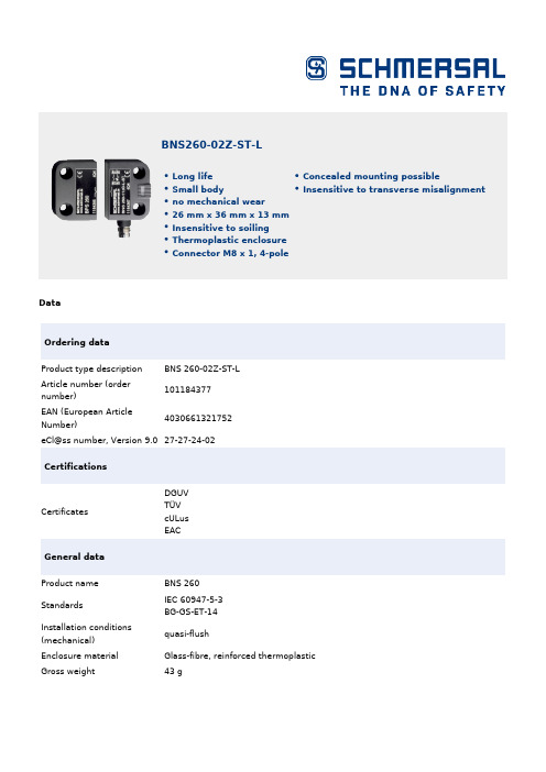
DataOrdering dataProduct type descriptionBNS 260-02Z-ST-L Article number (ordernumber)101184377EAN (European ArticleNumber)4030661321752eCl@ss number, Version 9.027-27-24-02CertificationsCertificates DGUVTÜVcULus EACGeneral dataProduct nameBNS 260StandardsIEC 60947-5-3 BG-GS-ET-14 Installation conditions(mechanical)quasi-flush Enclosure materialGlass-fibre, reinforced thermoplastic Gross weight 43 g BNS260-02Z-ST-LLong lifeSmall bodyno mechanical wear26 mm x 36 mm x 13 mmInsensitive to soilingThermoplastic enclosureConnector M8 x 1, 4-pole Concealed mounting possible Insensitive to transverse misalignmentGeneral data - FeaturesCoding YesNumber of openers2Number of safety contacts2Safety appraisalStandards ISO 13849-1Mission Time20 Year(s)Safety appraisal - Safety outputsB10d Normally-closed25,000,000 Operationscontact (NC)Mechanical dataActuating element MagnetDoor hinge LeftEnsured switch distance5 mm"ON" S aoEnsured switch distance15 mm"OFF" S arAxial misalignment, a horizontal and vertical misalignment of the safety sensorand the actuator are tolerated. The possible misalignment depends on thedistance of the active surfaces of the sensor and the actuator. The sensorremains active within the tolerance range.Direction of motion Head-on to the active surfaceMechanical data - Connection techniqueTerminal Connector Connector M8Mechanical data - DimensionsHeight of sensor36 mmLength of sensor13 mmWidth of sensor26 mmAmbient conditionsProtection class IP67Ambient temperature,-25 °CminimumAmbient temperature,+70 °CmaximumStorage and transport-25 °Ctemperature, minimumStorage and transport+70 °Ctemperature, maximumResistance to vibrations to10 … 55 Hz, amplitude 1 mmEN 60068-2-6Restistance to shock30 g / 11 msElectrical dataVoltage type DC (direct current)Switching voltage, maximum75 VDCSwitching current, maximum0.4 ASwitching capacity,10 VAmaximumSwitching frequency,5 HzmaximumScope of deliveryIncluded in delivery Actuators must be ordered separately.AccessoryRecommendation (actuator)BPS 260SRB-E-301STSRB-E-201LCNotesNote (General)The number in brackets indicate the PIN number of the connector. Circuit exampleNote (Wiring diagram)Contact S21-S22 and S11-S12 must be integrated in the safety circuit. Ordering codeProduct type description:BNS 260-(1)(2)Z(3)-(4)-(5)(1)11 1 NO contacts/1 NC contact02 2 NC contact(2)without with diagnostic output/01 1 NC contact(3)without without LED switching conditions displayG with LED switching conditions display(4)without Pre-wired cableST with connector(5)L Door hinge on left-hand sideR Door hinge on right-hand sidePicturesProduct picture (catalogue individual photo)ID: kbns2f04| 42,3 kB | .png | 74.083 x 60.325 mm - 210 x 171Pixel - 72 dpi| 63,6 kB | .jpg | 27.093 x 22.013 mm - 320 x 260 Pixel- 300 dpi| 540,4 kB | .jpg | 352.778 x 287.161 mm - 1000 x 814Pixel - 72 dpiDimensional drawing basic componentID: 1bns2g06| 65,1 kB | .jpg | 352.778 x 245.181 mm - 1000 x 695Pixel - 72 dpi| 18,6 kB | .jpg | 112.889 x 78.317 mm - 320 x 222Pixel - 72 dpi| 3,1 kB | .png | 74.083 x 51.506 mm - 210 x 146 Pixel- 72 dpi| 25,6 kB | .cdr |DiagramID: kbns2k25| 60,6 kB | .jpg | 352.778 x 70.203 mm - 1000 x 199Pixel - 72 dpiCharacteristic curveID: kbns2d03| 36,8 kB | .cdr || 40,4 kB | .jpg | 112.889 x 74.789 mm - 320 x 212Pixel - 72 dpi| 18,5 kB | .png | 74.083 x 49.036 mm - 210 x 139Pixel - 72 dpiCharacteristic curveID: kbns2d02| 19,2 kB | .png | 74.083 x 49.389 mm - 210 x 140Pixel - 72 dpi| 40,8 kB | .jpg | 112.889 x 75.142 mm - 320 x 213Pixel - 72 dpi| 36,3 kB | .cdr |ClipartID: kbns2c02| 1,8 kB | .png | 74.083 x 52.211 mm - 210 x 148 Pixel- 72 dpi| 19,6 kB | .cdr |Contact arrangementID: km8--k4b| 17,0 kB | .cdr |K.A. Schmersal GmbH & Co. KG, Möddinghofe 3, D-42279 WuppertalThe details and data referred to have been carefully checked. Images may diverge from original. Further technical data can be found in the manual. Technical amendments and errors possible.Generated on 08.07.2020 19:12:23。