XC3S200A_Lab1_Counter4_VHDL
Spartan-XC3S200AN-使用手册

14 System Clock 输入
Clock 输入为 40MHz 的振荡晶体
15 FPGA Suspend 设定
左边为+3.3V,右边为 GND
16 FPGA
Xilinx Spartan3S200-AN
17 RS232 串行接口
第二组 UART 界面
18 电源开关
往下为开启电源输入
19 8x8 LED 矩阵
NET “RESETN” LOC = “K5”;
##RESET 按键
NET "DIP_in<0>" LOC = "E6";
##DIP_Switch<0> 输入
13fpgaconfig模式设定m0m1m2短路代表开机为masterslavemode14systemclock输入clock输入为40mhz的振荡晶体15fpgasuspend设定左边为33v右边为gnd16fpgaxilinxspartan3s200an17rs232串行接口第二组uart界面18电源开关往下为开启电源输入198x8led矩阵8x8矩阵式led20led1616个led21pushbutton个按键输入22dip4个dipswitch输入左切为lowlogic23resetn提供使用者输入reset信号按下时为低电位24program按下时fpga会重新configuration25七节灯管四位的七节灯管26ps2键盘或鼠标接口27vga八色vga显示器输出
2-4. PUSH_BUTTON 与 DIP_SWITCH 输入
实验板上有 8 个 PUSH_BUTTON 与 4 个 DIP_SWICTH 与 1 个 RESET 按键与 1 个 PROGRAM,
基于XC3S400的实验板的VHDL程序设计报告
基于XC3S400的实验板的VHDL程序设计报告——实验一流水灯设计实验目的和要求:1、熟悉实验板XC3S400;2、掌握VHDL开发软件Xilinx ISE 8.2i和仿真软件ModleSim SE 6.2b的使用;3、掌握VHDL语言;4、了解基于实验板的程序设计过程。
实验环境:Windows XP系统、Xilinx ISE 8.2i、ModleSim SE 6.2b实验内容:1、搭建XC3S400实验板开发环境;2、设计一个程序,使4个发光二极管流水定时(比如每1秒钟)发光一次然后熄灭,按下一个按钮时能够使发光二极管全部熄灭(以下称流水灯功能);实验步骤:1、安装Xilinx ISE 8.2i 和ModleSim SE 6.2b,并设置ISE的默认仿真软件为ModleSim SE 6.2b。
2、在ISE中建立一个New Project。
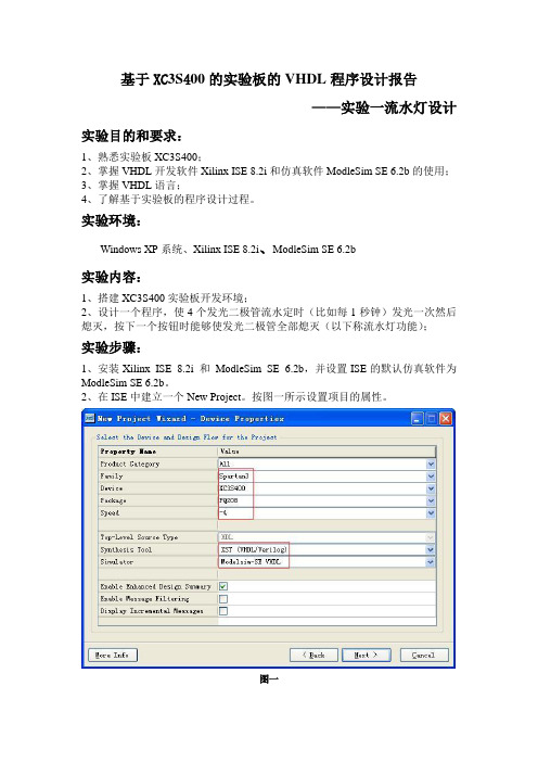
按图一所示设置项目的属性。
图一3、在项目中添加一个New Source。
选择VHDL Module文件类型,设置输入输出信号,点击Finish。
4、编写流水灯程序,用并在ModleSim中对程序进行前仿真并记录仿真结果。
5、对仿真通过的程序进行User Constranints。
首先运行Create Timing Constraints,按图二设置相关参数:图二然后运行Assign Package Pins,参照XC3S400开发板使用手册,进行管脚定义。
参考I/O管脚定义如图三所示(设置时钟CLK为LVTTL):图三6、运行Implement Design。
通过后,对程序进行后仿真,记录仿真结果。
7、运行Configure Device (iMPACT)将程序下载到开发板,观察程序运行结果并记录。
实验记录:1、流水灯源程序:(1)、时钟的分频处理。
建立一个New Source,选择IP (Coregen & Architecture Wizard)文件类型,选择FPGA Features and Design>>Clocking>>Virtex-II Pro…>>Single DCM v8.2i,点击Next。
XC3S200A_Lab3_LED
Lab3:LED.npl[实验说明] : 使用ISE9.1i设计LED跑马灯的VHDL语法与操作说明在这一个范例中,你将制作一个LED的模块,与此项目所需的UCF 文件.利用上一个范例中的分频模块,将40MHz的外部Clock频率除频为10Hz,提供跑马灯电路使用.透过JTAG接口连接烧录到C3S200A_FT256开发板中,验证其设计结果是否正确? 此设计同时利用ISE9.1i 的仿真功能来验证结果的正确性?.[实验目地] : 当你完成整个项目之后,你将学会以下的功能.(1).利用ISE9.1i 的软件开启一个Spartan3A FPGA 的项目.(2).撰写一个简单的VHDL 程序,利用语法检查器(Syntax Check)来修正语法的错误(3).产生测试模板(Test Pattern) 来辅助你的设计.(4).加入系统所需的Constraints 文件.(UCF file)(5).完成整个设计流程.并产生LED.bit文件。
(6).利用FPGA Editor 来察看FPGA 内部的结果,(7).利用[Impact] 来烧录LED.bit 文件到FPGA.[系统需求]:PC 个人计算机ISE9.1i 软件LED.VHD 文件LED.UCF 文件Platform Cable USBXC3S200A_FT256开发板电源供应器(DC5V 输入).[系统设计说明]以跑马灯的概念,设计到电路中,并以LED输出显示[操作步骤]:(1)开启ISE9.1i软件: [程序集] → [Xilinx ISE 9.1i] → [Project Navigator] . 会出现ISE9.1i 的画面,画面开启之初, 会出现[Tip of the Day], 可以将之关掉后,出现以下的画面.(2).在ISE9.1 软件环境下,开启一个新的工程: [File] [New Project][Project Name] : Lab3_LED[Project Location]: c: \Lab3_LED (依使用者设定的目录).[Top-Level Module Type] : HDL( 代表最上层的设计模块是以HDL 输方方式的模组.(3).下一个画面就是设定硬件FPGA的参数[FPGA系列(Device Family)]:Spartan3A( 请看板子的FPGA FPGA的编号)[FPGA名称(Device)] : XC3S200A(请参考开发板的FPGA FPGA的编号)[FPGA包装(Package)]:FT256(请参考开发板的FPGA FPGA的编号)[FPGA速度等级(Speed)]: -4 ( FPGA 速度等级)[综合工具(Synthesis Tool)]:XST VHDL(VHDL综合的种类)[仿真器(Simulator)] : ISE Simulator(ISE9.1 内建的仿真器)[产生仿真器的语言(Generated Simulation Language)] : VHDL(4).下一个画面Create a New Source 先跳过,按[下一步]. 下一个画面Add a Existing Source 亦跳过,按[下一步]. 此时出现此项目所有设定的信息,若需重新设定,则可[上一步]. 若无误,则按[完成];(5).此时出现一个项目的架构,可以允许使用者开始进行项目的设计.(6).加入新的设计文件: [Project] [New Source];选择VHDL Module,并设定文件名称为LED(7).利用Wizard,设定此设计的输出输入信号.Clockn : input (频率振荡晶体的输入信号).Reset : input (当Reset = ‘0’ 时,清除内部计数器LED_out : Output (跑马灯输出信号)(8).按[下一步],再按[完成];此时项目加入此模块之后,在Source In Project 的窗口中会出现LED.vdh 在专案中.(9).以鼠标双击LED.vhd 之后,在右边的工作区可以看到LED.vhd 的文件内容,此时可以修改或改变设计内容,在修改完成之后,利用[File] [Save]来储存文件. 在撰写LED.vhd 内容之时,可以參考ISE所附的Language Templatesignal count_mhz : std_logic_vector( 7 downto 0);===========================================GEN_1MHZ : process(Reset,clock)beginif Reset='0' thenmhz <= '0';count_mhz <= (others => '0');elsif Rising_edge(clock) thencount_mhz <= count_mhz + '1';if count_mhz = 40 thenmhz <= '1';count_mhz <= (others => '0');elsemhz <= '0';end if;end if;end process GEN_1MHZ;clk_1MHz<=mhz;process(clkdiv,sw)beginif Reset='0' thencount<="0000";sw<='0';elsif rising_edge(clkdiv) thenif sw='0' thencount<=count+1;if count=6 thensw<='1';end if;end if;if sw='1' thencount<=count-1;if count=0 thensw<='0';end if;end if;end if;end process;with count SELectLED_out<= "1100000000000011" when "0001", --1"1110000000000111" when "0010", --2"1111000000001111" when "0011", --3"1111100000011111" when "0100", --4"1111110000111111" when "0101", --5"1111111001111111" when "0110", --6"1111111111111111" when "0111", --7"1000000000000001" when others; --0(10).第一次进行编译的工作,以确认设计的正确性与否?在[Project ]的窗口中,直接以鼠标双击Generate Programming File 的选项.此时ISE9.1 会自动执行并产生可以Download 的.bit 文件,此步骤是最直接验证设计工作的正确性与否?若在每一个程序都出现打勾,代表O.K.若有一个程序都出现打叉[X]的符号,代表有错误,可以依显示结果来侦错.(11).在实际烧录FGPA之前位了要验证设计的正确性,可以先利用测试模板(Testbench)来验证设计的正确性.(12).依使用者需求更改输入端数据,已达到验证效果,设定完后存盘进行仿真,但是此设计电路有经过一个分频器,所以在进行模拟之前,先把分频器拿掉,这样可以缩短仿真花费的时间.(13).在[Sources]选取[Behavioral Simulation]→[Processes] →[ModelSim Simulator]→双击[Simulate Behavioral Model],执行之后,出现仿真的结果.(14) 同样地,选择[Simulate Post Place & Route HDL Model] 来查看经过Place and Route 之后,含有时间延迟的输出波形, 并且利用[Measure Meter] 来量测其延迟的时间(15). 再来需设定I/O 脚的位置,可以利用LED.UCF 来设定I/O 脚的位置,以得到正确的输出文件.۞[Project] [New Source]. 设定输入的文件格式为[Implementation Constraints File] 文件名称为ELD(自动储存为LED.UCF)(16).点选[Source in Project]窗口内的LED.ucf,利用Assign Package Pins 中的[LOC]之接输入输出脚的脚位,也可以利用鼠标点选信号后,以鼠标拖曳到右边的脚位上即可,输入后储存文件.(相关脚位定义请參考使用手册得知).NET "LED_out<1>" LOC = "M13" ;NET "LED_out<2>" LOC = "K13" ;NET "LED_out<3>" LOC = "L13" ;NET "LED_out<4>" LOC = "M16" ;NET "LED_out<5>" LOC = "M15" ;NET "LED_out<6>" LOC = "L16" ;NET "LED_out<7>" LOC = "L14" ;NET "LED_out<8>" LOC = "J13" ;NET "LED_out<9>" LOC = "J12" ;NET "LED_out<10>" LOC = "K14" ;NET "LED_out<11>" LOC = "K15" ;NET "LED_out<12>" LOC = "J16" ;NET "LED_out<13>" LOC = "K16" ;NET "LED_out<14>" LOC = "H14" ;NET "LED_out<15>" LOC = "J14" ;NET "Reset" LOC = K5;NET "Clock" LOC = P9;NET "LED_out<0>" LOC = M14;(17). 重新执行Generate Programming File, 确认设计无误(惊叹号为警告,但电路设计没有错误,无须检错).(18)若想要知道FPGA 最后实现在芯片内的状态,则可以[Project View] 窗口内的[Implement Design] → [Place and Route] → [View/Edit Routed Design(FPGA Editor)] 来查看其最后实现在FPGA 内部的状态.(19)在[Process for Source]窗口中,点选[View Design Summary], 可以浏览项目设计的报告, 包含FPGA 使用率,Report …..(20).在完成设计验证之后,就可以将LED.bit 写入到FPGA 内部,此时点选[Project View] 窗口内的[Generate Programming File] → [Configure Device (iMPACT) ],出现Impact 的窗口.(21)选取[Finish],进入自动联机,请事先连接JTAG接口与供应板子电压.(22) 此时JTAG Cable 会扫描JTAG Chain 的路径中的FPGA FPGA,若扫描成功则出现所扫描的FPGA,并跳出选择文件的窗口.选择文件之后,出现警告的窗口,按[确定],进入下一步.(23)此时出现的窗口,则表示出XC3S200A 的待烧录文件为Counter4.bit.以鼠标点选FPGA 会变为绿色,同时出现[Program Options] 窗口,按[OK] 开始烧录.(24)FPGA 若烧录成功,则出现Programming Succeeded 若programming 成功(25)可以在XC3S200A_FT256展示板LED看到跑马灯的验证。
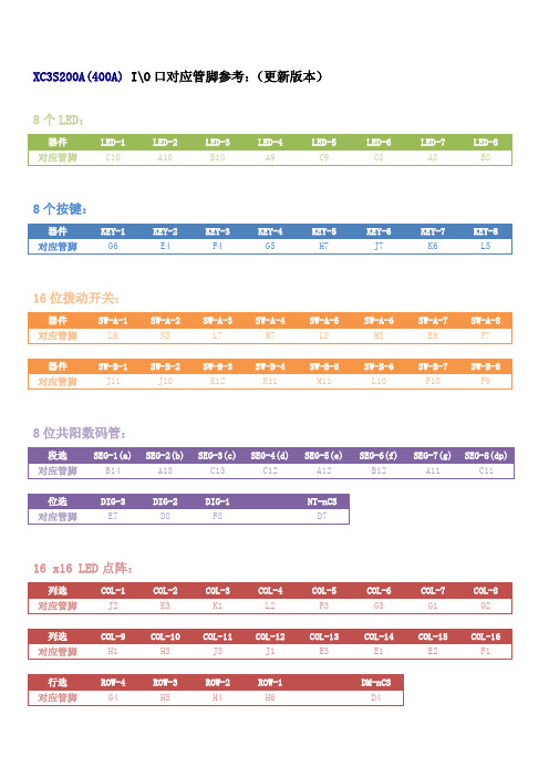
IO口对应管脚
ADDR-11 M4
ADDR-12 L4
ADDR-13 K4
ADDR-14 J4
ADDR-15 J6
地址线 对应管脚
ADDR-16 T6
ADDR-17 R1
ADDR-18 P2
ADDR-19 M1
ADDR-20 N2
ADDR-21 N3
数据线 对应管脚
DATA-0 N12
DATA-1 P11
DATA-2 R11
KEY-4 G5
KEY-5 H7
KEY-6 J7
KEY-7 K6
KEY-8 L5
16 位拨动开关:
器件 对应管脚
SW-A-1 L6
SW-A-2 N5
器件 对应管脚
SW-B-1 J11
SW-B-2 J10
SW-A-3 L7
SW-B-3 K12
SW-A-4 M7
SW-B-4 K11
SW-A-5 L8
SW-B-5 M11
FLA-OE N11
FLA-WE N1
FLA-RB P1
FLA-BYTE P6
34 外扩 I\O 口:
接口 对应管脚
I\O-1 GND
I\O-2 J12
接口 对应管脚
I\O-9 M14
I\O-10 N14
接口 对应管脚
I\O-17 J16
I\O-18 K15
接口 对应管脚
I\O-25 F16
I\O-26 F15
LM-CR D10
LM-INT D9
I2C SDA E13
I2C SCL F13
AD 转换器:
器件 对应管脚
AD-nCS P13
AD-CLK T13
基于FPGA和VHDL的电子秒表设计
基于FPGA和VHDL的电子秒表设计作者:赵云霞来源:《硅谷》2013年第14期摘要本文利用Spartan3A and Spartan3AN系列的XC3S200A FT256的FPGA作为开发硬件,ISE软件和ModelSim软件作为开发软件,设计制作了一款计数长度为一小时,计数精度为0.01秒,六位数码管显示的电子跑表。
具有开始/停止,复位清零功能,并且加入了扩展要求的多次暂停计数功能和消抖判断。
具有精度高,操作简单的特点。
关键词 FPGA;VHDL;ISE;ModelSim;电子跑表中图分类号:TP302 文献标识码:A 文章编号:1671-7597(2013)14-0025-01随着集成电路(IC)技术的发展,电子设计自动化(EDA)逐渐成为重要的设计手段,已经广泛应用于模拟与数字电路系统等许多领域。
而电子设计自动化(EDA)的实现是与CPLD/FPGA技术的迅速发展息息相关的,利用PLD/FPGA,电子系统设计工程师可以在实验室中设计出专用IC,实现了系统的集成。
此外,CPLD/FPGA还具有静态可重复编程或在线动态重构特性,使硬件的功能可像软件一样通过编程来修改,不仅使设计修改和产品升级变得十分方便,而且极大地提高了电子系统的灵活性和通用能力。
20世纪80年代后期由美国国防部开发的VHDL语言恰好满足了上述这样的要求,并在1987年12月由IEEE标准化。
它的出现为电子设计自动化(EDA)的普及和推广奠定了坚实的基础。
由此,使用VHDL语言来设计数字系统是电子设计技术的大势所趋。
1 系统电路设计系统由石英震荡器、分频部分、计数部分、显示部分、开始/停止使能和清零部分构成。
分频器将晶振所提供的48 MHz信号分频成100 Hz时钟信号作为最低位计数器的计时信号,将六个计数器异步级联得到跑表时间数据,再经过数据选择器和显示译码器,以动态显示模式将显示译码器的段选信号分位输出给六个8段LED数码管显示,开始/停止使能可实现暂停/继续计时操作,清零部分完成系统的时间清零,为下次计时做准备。
FPGA可编程逻辑器件芯片XC3S200A-4VQG100C中文规格书
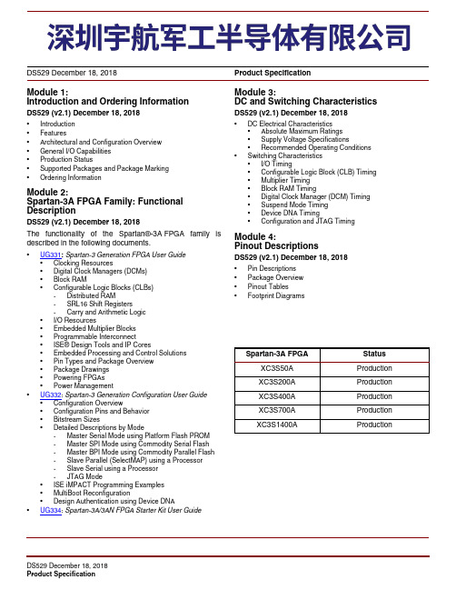
Module 3: DC and Switching Characteristics
DS529 (v2.1) December 18, 2018
• DC Electrical Characteristics • Absolute Maximum Ratings • Supply Voltage Specifications • Recommended Operating Conditions
• UG332: Spartan-3 Generation Configuration User Guide • Configuration Overview • Configuration Pins and Behavior • Bitstream Sizes • Detailed Descriptions by Mode - Master Serial Mode using Platform Flash PROM - Master SPI Mode using Commodity Serial Flash - Master BPI Mode using Commodity Parallel Flash - Slave Parallel (SelectMAP) using a Processor - Slave Serial using a Processor - JTAG Mode • ISE iMPACT Programming Examples • MultiBoot Reconfiguration • Design Authentication using Device DNA
DS529 (v2.1) December 18, 2018
FPGA可编程逻辑器件芯片XC3S200A-4FG320I中文规格书
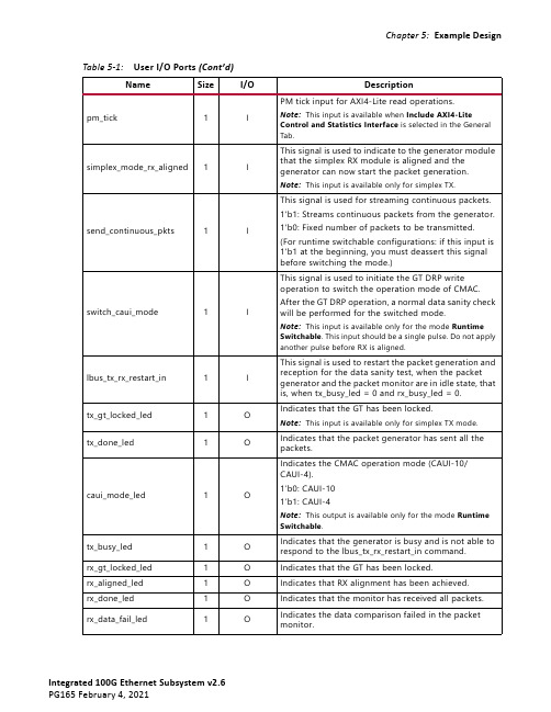
pm_tick 1I PM tick input for AXI4-Lite read operations.Note:This input is available when Include AXI4-LiteControl and Statistics Interface is selected in the GeneralTab.simplex_mode_rx_aligned 1I This signal is used to indicate to the generator module that the simplex RX module is aligned and the generator can now start the packet generation.Note:This input is available only for simplex TX.send_continuous_pkts 1I This signal is used for streaming continuous packets.1'b1: Streams continuous packets from the generator.1'b0: Fixed number of packets to be transmitted.(For runtime switchable configurations: if this input is 1'b1 at the beginning, you must deassert this signal before switching the mode.)switch_caui_mode 1I This signal is used to initiate the GT DRP write operation to switch the operation mode of CMAC.After the GT DRP operation, a normal data sanity check will be performed for the switched mode.Note:This input is available only for the mode RuntimeSwitchable . This input should be a single pulse. Do not applyanother pulse before RX is aligned.lbus_tx_rx_restart_in 1I This signal is used to restart the packet generation and reception for the data sanity test, when the packet generator and the packet monitor are in idle state, that is, when tx_busy_led = 0 and rx_busy_led = 0.tx_gt_locked_led 1O Indicates that the GT has been locked.Note:This input is available only for simplex TX mode.tx_done_led 1OIndicates that the packet generator has sent all the packets.caui_mode_led 1O Indicates the CMAC operation mode (CAUI-10/CAUI-4).1’b0: CAUI-101’b1: CAUI-4Note:This output is available only for the mode RuntimeSwitchable .tx_busy_led1O Indicates that the generator is busy and is not able to respond to the lbus_tx_rx_restart_in command.rx_gt_locked_led1O Indicates that the GT has been locked. rx_aligned_led1O Indicates that RX alignment has been achieved.rx_done_led1O Indicates that the monitor has received all packets.rx_data_fail_led 1O Indicates the data comparison failed in the packet monitor.Table 5-1:User I/O Ports (Cont’d)NameSize I/O Descriptiongt_rxcdrhold10/4I Refer to the applicable GT user guide for the port description.[Ref11][Ref12]Note:This port is available when Enable Additional GT Control/Status and DRP Ports is selected from the CMAC / GT Selection and Configuration tab.Port width: 10-bit for CAUI-10 or Runtime Switchable case, and 4-bit width for CAUI-4 mode.gt_rxpolarity10/4I Refer to the applicable GT user guide for the port description.[Ref11][Ref12]Note:This port is available when Enable Additional GT Control/Status and DRP Ports is selected from the CMAC / GT Selection and Configuration tab.Port width: 10-bit for CAUI-10 or Runtime Switchable case, and 4-bit width for CAUI-4 mode.gt_rxrate30/12I Refer to the applicable GT user guide for the port description.[Ref11][Ref12]Note:This port is available when Enable Additional GT Control/Status and DRP Ports is selected from the CMAC / GT Selection and Configuration tab.Port width: 30-bit for CAUI-10 or Runtime Switchable case, and 12-bit width for CAUI-4 mode.gt_txdiffctrl50/20I Refer to the applicable GT user guide for the port description.[Ref11][Ref12]Note:This port is available when Enable Additional GT Control/Status and DRP Ports is selected from the CMAC / GT Selection and Configuration tab.Port width: 50-bit for CAUI-10 or Runtime Switchable case, and 20-bit width for CAUI-4 mode.gt_txpolarity10/4I Refer to the applicable GT user guide for the port description.[Ref11][Ref12]Note:This port is available when Enable Additional GT Control/Status and DRP Ports is selected from the CMAC / GT Selection and Configuration tab.Port width: 10-bit for CAUI-10 or Runtime Switchable case, and 4-bit width for CAUI-4 mode.gt_txinhibit10/4I Refer to the applicable GT user guide for the port description.[Ref11][Ref12]Note:This port is available when Enable Additional GT Control/Status and DRP Ports is selected from the CMAC / GT Selection and Configuration tab.Port width: 10-bit for CAUI-10 or Runtime Switchable case, and 4-bit width for CAUI-4 mode.Table 5-2:CORE XCI Top-Level Port List (Cont’d)Name Size I/O DescriptionChapter 5:Example Designgt0_drpwe1I Refer to the applicable GT user guide for the port description.[Ref11][Ref12]Note:This port is available when Enable Additional GT Control/Status and DRP Ports is selected from the CMAC / GT Selection and Configuration tab.gt0_drpaddr10I Refer to the applicable GT user guide for the port description.[Ref11][Ref12]Note:This port is available when Enable Additional GT Control/Status and DRP Ports is selected from the CMAC / GT Selection and Configuration tab.gt0_drpdi16I Refer to the applicable GT user guide for the port description.[Ref11][Ref12]Note:This port is available when Enable Additional GT Control/Status and DRP Ports is selected from the CMAC / GT Selection and Configuration tab.gt0_drpdo16O Refer to the applicable GT user guide for the port description.Note:This port is available when Enable Additional GT Control/Status and DRP Ports is selected from the CMAC / GT Selection and Configuration tab.gt0_drprdy1O Refer to the applicable GT user guide for the port description.[Ref11][Ref12]Note:This port is available when Enable Additional GT Control/Status and DRP Ports is selected from the CMAC / GT Selection and Configuration tab.gt1_drpen1I Refer to the applicable GT user guide for the port description.[Ref11][Ref12]Note:This port is available when Enable Additional GT Control/Status and DRP Ports is selected from the CMAC / GT Selection and Configuration tab.gt1_drpwe1I Refer to the applicable GT user guide for the port description.[Ref11][Ref12]Note:This port is available when Enable Additional GT Control/Status and DRP Ports is selected from the CMAC / GT Selection and Configuration tab.gt1_drpaddr10I Refer to the applicable GT user guide for the port description.[Ref11][Ref12]Note:This port is available when Enable Additional GT Control/Status and DRP Ports is selected from the CMAC / GT Selection and Configuration tab.gt1_drpdi16I Refer to the applicable GT user guide for the port description.[Ref11][Ref12]Note:This port is available when Enable Additional GT Control/Status and DRP Ports is selected from the CMAC / GT Selection and Configuration tab.Table 5-2:CORE XCI Top-Level Port List (Cont’d)Name Size I/O Description。
FPGA可编程逻辑器件芯片XC3S200A-5FGG320C中文规格书
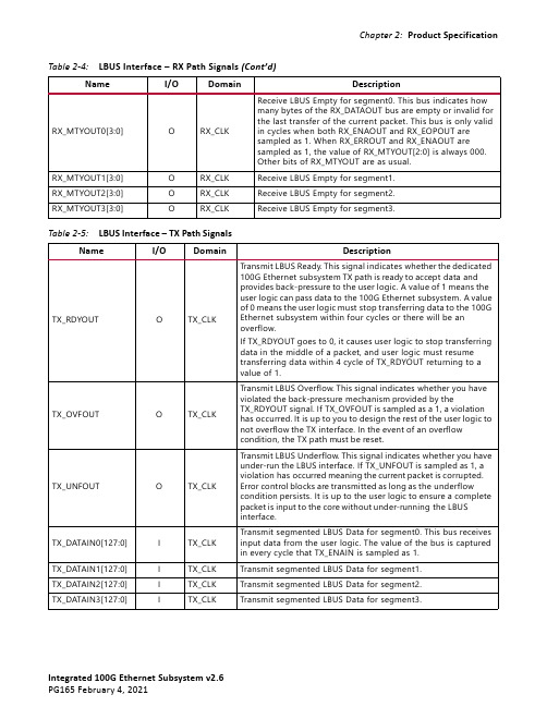
RX_MTYOUT0[3:0]O RX_CLK Receive LBUS Empty for segment0. This bus indicates how many bytes of the RX_DATAOUT bus are empty or invalid for the last transfer of the current packet. This bus is only valid in cycles when both RX_ENAOUT and RX_EOPOUT are sampled as 1. When RX_ERROUT and RX_ENAOUT are sampled as 1, the value of RX_MTYOUT[2:0] is always 000. Other bits of RX_MTYOUT are as usual.RX_MTYOUT1[3:0]O RX_CLK Receive LBUS Empty for segment1.RX_MTYOUT2[3:0]O RX_CLK Receive LBUS Empty for segment2.RX_MTYOUT3[3:0]O RX_CLKReceive LBUS Empty for segment3. Table 2-4:LBUS Interface – RX Path Signals (Cont’d)Name I/O Domain DescriptionTable 2-5:LBUS Interface – TX Path Signals Name I/O Domain DescriptionTX_RDYOUT O TX_CLK Transmit LBUS Ready. This signal indicates whether the dedicated 100G Ethernet subsystem TX path is ready to accept data and provides back-pressure to the user logic. A value of 1 means the user logic can pass data to the 100G Ethernet subsystem. A value of 0 means the user logic must stop transferring data to the 100G Ethernet subsystem within four cycles or there will be an overflow.If TX_RDYOUT goes to 0, it causes user logic to stop transferring data in the middle of a packet, and user logic must resume transferring data within 4 cycle of TX_RDYOUT returning to a value of 1.TX_OVFOUT O TX_CLK Transmit LBUS Overflow. This signal indicates whether you have violated the back-pressure mechanism provided by the TX_RDYOUT signal. If TX_OVFOUT is sampled as a 1, a violation has occurred. It is up to you to design the rest of the user logic to not overflow the TX interface. In the event of an overflow condition, the TX path must be reset.TX_UNFOUT O TX_CLK Transmit LBUS Underflow. This signal indicates whether you have under-run the LBUS interface. If TX_UNFOUT is sampled as 1, a violation has occurred meaning the current packet is corrupted. Error control blocks are transmitted as long as the underflow condition persists. It is up to the user logic to ensure a complete packet is input to the core without under-running the LBUS interface.TX_DATAIN0[127:0]I TX_CLK Transmit segmented LBUS Data for segment0. This bus receives input data from the user logic. The value of the bus is captured in every cycle that TX_ENAIN is sampled as 1.TX_DATAIN1[127:0]I TX_CLK Transmit segmented LBUS Data for segment1.TX_DATAIN2[127:0]I TX_CLK Transmit segmented LBUS Data for segment2.TX_DATAIN3[127:0]I TX_CLKTransmit segmented LBUS Data for segment3.STAT_RX_FRAMING_ERR_VALID_4O RX_CLK Valid indicator forSTAT_RX_FRAMING_ERR_4[3:0].STAT_RX_FRAMING_ERR_VALID_5O RX_CLK Valid indicator forSTAT_RX_FRAMING_ERR_5[3:0].STAT_RX_FRAMING_ERR_VALID_6O RX_CLK Valid indicator forSTAT_RX_FRAMING_ERR_6[3:0].STAT_RX_FRAMING_ERR_VALID_7O RX_CLK Valid indicator forSTAT_RX_FRAMING_ERR_7[3:0].STAT_RX_FRAMING_ERR_VALID_8O RX_CLK Valid indicator forSTAT_RX_FRAMING_ERR_8[3:0].STAT_RX_FRAMING_ERR_VALID_9O RX_CLK Valid indicator forSTAT_RX_FRAMING_ERR_9[3:0].STAT_RX_FRAMING_ERR_VALID_10O RX_CLK Valid indicator forSTAT_RX_FRAMING_ERR_10[3:0].STAT_RX_FRAMING_ERR_VALID_11O RX_CLK Valid indicator forSTAT_RX_FRAMING_ERR_11[3:0].STAT_RX_FRAMING_ERR_VALID_12O RX_CLK Valid indicator forSTAT_RX_FRAMING_ERR_12[3:0].STAT_RX_FRAMING_ERR_VALID_13O RX_CLK Valid indicator forSTAT_RX_FRAMING_ERR_13[3:0].STAT_RX_FRAMING_ERR_VALID_14O RX_CLK Valid indicator forSTAT_RX_FRAMING_ERR_14[3:0].STAT_RX_FRAMING_ERR_VALID_15O RX_CLK Valid indicator forSTAT_RX_FRAMING_ERR_15[3:0].STAT_RX_FRAMING_ERR_VALID_16O RX_CLK Valid indicator forSTAT_RX_FRAMING_ERR_16[3:0].STAT_RX_FRAMING_ERR_VALID_17O RX_CLK Valid indicator forSTAT_RX_FRAMING_ERR_17[3:0].STAT_RX_FRAMING_ERR_VALID_18O RX_CLK Valid indicator forSTAT_RX_FRAMING_ERR_18[3:0].STAT_RX_FRAMING_ERR_VALID_19O RX_CLK Valid indicator forSTAT_RX_FRAMING_ERR_19[3:0].STAT_RX_LOCAL_FAULT O RX_CLK This output is High whenSTAT_RX_INTERNAL_LOCAL_FAULT or STAT_RX_RECEIVED_LOCAL_FAULT is asserted. This output is level sensitive.Table 2-7:LBUS Interface – RX Path Control/Status Signals (Cont’d)Name I/O Domain DescriptionChapter 2:Product SpecificationSTAT_RX_PCSL_NUMBER_18[4:0]O RX_CLK This signal indicates which PCS lane isreceived on physical lane 18.STAT_RX_PCSL_NUMBER_19[4:0]O RX_CLK This signal indicates which PCS lane isreceived on physical lane 19.STAT_RX_PCSL_DEMUXED[19:0]O RX_CLK PCS Lane Marker found. If a signal of this bus is sampled as 1, it indicates that the receiver has properly de-multiplexed that PCS lane. These outputs are level sensitive.STAT_RX_BAD_FCS[3:0]O RX_CLK Bad FCS indicator. A value of 1 indicates a packet was received with a bad FCS, but not a stomped FCS. A stomped FCS is defined as the bitwise inverse of the expected good FCS. This output is pulsed for one clock cycle to indicate an error condition. Pulses can occur in back-to-back cycles.STAT_RX_STOMPED_FCS[3:0]O RX_CLK Stomped FCS indicator. A value of 1 or greater indicates that one or more packets were received with a stomped FCS. A stomped FCS is defined as the bitwise inverse of the expected good FCS. This output is pulsed for one clock cycle to indicate the stomped condition. Pulses can occur in back-to-back cycles.STAT_RX_TRUNCATED O RX_CLK Packet truncation indicator. A value of 1 indicates that the current packet in flight is truncated due to its length exceeding CTL_RX_MAX_PACKET_LEN[14:0]. This output is pulsed for one clock cycle to indicate the truncated condition. Pulses can occur in back-to-back cycles.STAT_RX_INTERNAL_LOCAL_FAULT O RX_CLK This signal goes High when an internal local fault is generated due to any one of the following: test pattern generation, bad lane alignment, or high bit error rate. This signal remains High as long as the fault condition persists.STAT_RX_RECEIVED_LOCAL_FAULT O RX_CLK This signal goes High when enough local fault words are received from the link partner to trigger a fault condition as specified by the IEEE fault state machine. This signal remains High as long as the fault condition persists.Table 2-7:LBUS Interface – RX Path Control/Status Signals (Cont’d)Name I/O Domain Description。
FPGA可编程逻辑器件芯片XC3S200-4FG676C中文规格书
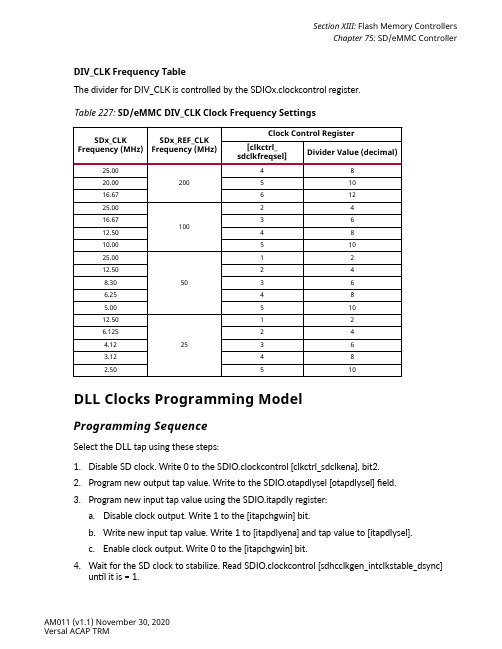
DIV_CLK Frequency TableThe divider for DIV_CLK is controlled by the SDIOx.clockcontrol register.Table 227: SD/eMMC DIV_CLK Clock Frequency SettingsSDx_CLK Frequency (MHz)SDx_REF_CLK Frequency (MHz)Clock Control Register [clkctrl_sdclkfreqsel]Divider Value (decimal)25.002004820.0051016.6761225.001002416.673612.504810.0051025.00501212.50248.30366.25485.0051012.5025126.125244.12363.12482.50510DLL Clocks Programming ModelProgramming SequenceSelect the DLL tap using these steps:1.Disable SD clock. Write 0 to the SDIO.clockcontrol [clkctrl_sdclkena], bit2.2.Program new output tap value. Write to the SDIO.otapdlysel [otapdlysel] field.3.Program new input tap value using the SDIO.itapdly register:a.Disable clock output. Write 1 to the [itapchgwin] bit.b.Write new input tap value. Write 1 to [itapdlyena] and tap value to [itapdlysel].c.Enable clock output. Write 0 to the [itapchgwin] bit.4.Wait for the SD clock to stabilize. Read SDIO.clockcontrol [sdhcclkgen_intclkstable_dsync]until it is = 1.Section XIII: Flash Memory ControllersChapter 75: SD/eMMC Controller5.Enable the SD clock. Write 1 to [clkctrl_sdclkena].Note: In auto-tune mode, the tuning logic might wait for the SDIO.clockcontrol[sdhcclkgen_intclkstable_dsync, 1] each time before issuing the read tuning command to the SD card.I/O ClocksThe I/O timing has several modes depending on the interface mode and the clock frequency.The TX interface has two clock modes:•AXI and APB Isolation•TX Clocking > 25 MHz using DLL clocking with 180-tap unitThe RX interface has two clock modes:•25 MHz Clocking with SCLK clock looped back•RX Clocking >25 MHz using DLL clocking with 180-tap unitSCLK Clock EdgeThe SCLK clock edge that is used to drive and latch data. The clock edges are defined by the controller mode. The active clock edge for each mode is listed in the tables in Speed Modes.RX/TX Tuning MethodsThe tuning methods are shown in the following table.Table 228: Tuning MethodsControllerMode Speed Mode Clock Rate(MHz)Tuning MethodDLL RX TapsSD Default speed25~High speed50Manual SDR-1225~SDR-2550Manual DDR-5050Manual SDR-50100Auto-tuning SDR-104200Auto-tuningTable 228: Tuning Methods (cont'd)ControllerMode Speed Mode Clock Rate(MHz)Tuning MethodDLL RX TapseMMC Legacy MMC25~HS-SDR50Manual HS-DDR50Manual HS-200200Auto-tuningAuto Tuning NoteDuring auto-tuning, one of the following must occur before sending any command sequence including CMD19, CMD21, or any other command sequence:•SDx.clockcontrol [sdhcclkgen_intclkstable_dsync] (bit 1) reads = 1•PMC_IOP_SLCR.SDx_DLL_CTRL [SDx_DLL_PSDONE] reads = 1The maximum number of tap delays in DLL mode (phases of the clock) is 180, but the useful number of tap delays is reduced as the clock frequency goes up.25 MHz ClockingAt <= 25 MHz, the RX interface is clocked by a clock signal that is looped back from the SCLK output pad. The SCLK output is driven by the DIV_CLK.The TX interface is clocked by the TX_CLK, which is multiplexed from the DIV_CLK derived from the 10-bit counter. The clock edge timing is fixed and cannot be adjusted.The clock structure is shown in I/O Clock Block Diagram. The frequency control is explained in DIV_CLK Programming Model.TX Clocking > 25 MHzFor clock frequencies greater than 25 MHz, the DLL generates the DLL_IO_CLK for the I/O SCLK output and the DLL_TX_CLK for the TX interface to drive the command and data output signals.•DLL_IO_CLK to the SCLK clock output pad•DLL_TX_CLK to the TX interface for clocking-out the command and data output padsThe DLL_TX_CLK does not affect the SCLK output.The timing of the DLL_TX_CLK relative to the DLL_IO_CLK is adjusted using a 180-tap unit. The TX tap for DLL_TX_CLK is selected by the SDIO.sd0_otapdlysel [otapdlysel] bit field. The clock frequency determines the number of useful taps.。
FPGA可编程逻辑器件芯片XC3S200AN-5FTG256I中文规格书
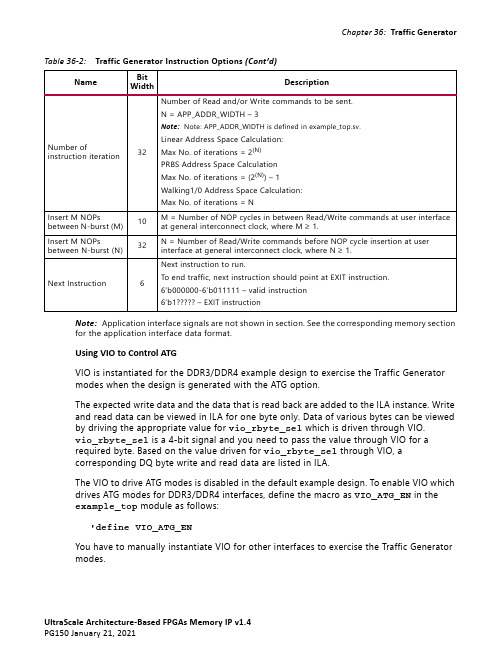
Note:Application interface signals are not shown in section. See the corresponding memory section for the application interface data format.Using VIO to Control ATGVIO is instantiated for the DDR3/DDR4 example design to exercise the Traffic Generator modes when the design is generated with the ATG option.The expected write data and the data that is read back are added to the ILA instance. Write and read data can be viewed in ILA for one byte only. Data of various bytes can be viewed by driving the appropriate value for vio_rbyte_sel which is driven through VIO. vio_rbyte_sel is a 4-bit signal and you need to pass the value through VIO for a required byte. Based on the value driven for vio_rbyte_sel through VIO, a corresponding DQ byte write and read data are listed in ILA.The VIO to drive ATG modes is disabled in the default example design. To enable VIO which drives ATG modes for DDR3/DDR4 interfaces, define the macro as VIO_ATG_EN in the example_top module as follows:‘define VIO_ATG_ENYou have to manually instantiate VIO for other interfaces to exercise the Traffic Generator modes.Number of instruction iteration 32Number of Read and/or Write commands to be sent.N = APP_ADDR_WIDTH – 3Note:Note: APP_ADDR_WIDTH is defined in example_top.sv.Linear Address Space Calculation:Max No. of iterations = 2(N)PRBS Address Space CalculationMax No. of iterations = (2(N)) – 1Walking1/0 Address Space Calculation:Max No. of iterations = NInsert M NOPs between N-burst (M)10M = Number of NOP cycles in between Read/Write commands at user interface at general interconnect clock, where M ≥ 1.Insert M NOPs between N-burst (N)32N = Number of Read/Write commands before NOP cycle insertion at user interface at general interconnect clock, where N ≥ 1.Next Instruction 6Next instruction to run.To end traffic, next instruction should point at EXIT instruction.6’b000000-6’b011111 – valid instruction6’b1????? – EXIT instruction Table 36-2:Traffic Generator Instruction Options (Cont’d)Name Bit WidthDescriptionThe ATG default control connectivity in the example design created by Vivado is listed in Table36-3.Note:Application interface signals are not shown in this table. See the corresponding memorysection for application interface address/data width.Table 36-3:Default Traffic Generator Control ConnectionSignal I/O Width Description Default Valueclk I1Traffic Generator Clock Traffic G eneratorClockrst I1Traffic Generator Reset Traffic G eneratorResetinit_calib_complete I1Calibration Complete CalibrationCompleteGeneral Controlvio_tg_start I1Enable traffic generator to proceed from"START" state to "LOAD" state after calibrationcompletes.If you do not plan to program instruction tableor PRBS data seed, tie this signal to 1'b1.If you plan to program instruction table or PRBSdata seed, set this bit to 0 during reset. Afterreset deassertion and done with instruction/seed programming, set this bit to 1 to starttraffic generator.Reserved signal.Tie to 1'b1.vio_tg_rst I1Reset traffic generator (synchronous reset, level sensitive).If there is outstanding traffic in memorypipeline, assert signal by some number of clockcycles until all outstanding transactions havecompleted.Reserved signal.Tie to 0.vio_tg_restart I1Restart traffic generator after generator is donewith traffic, paused or stopped with error (level sensitive).If there is outstanding traffic in memorypipeline, assert signal by some number of clockcycles until all outstanding transactions havecompleted.Reserved signal.Tie to 0.vio_tg_pause I1Pause traffic generator (level sensitive).Reserved signal.Tie to 0.vio_tg_err_chk_en I1If enabled, stop after first error detected. Readtest is performed to determine whether "READ"or "WRITE" error occurred. If not enabled,continue traffic without stop.Reserved signal.Tie to 0.Chapter 36:Traffic Generatorvio_tg_err_clear I1Clear all error excluding sticky error bit(positive edge sensitive).Only use this signal when vio_tg_status_state iseither TG_INSTR_ERRDONE orTG_INSTR_PAUSE. Error is cleared two cyclesafter vio_tg_err_clear is asserted.Reserved signal.Tie to 0.vio_tg_err_clear_all I1Clear all error including sticky error bit (positiveedge sensitive).Only use this signal when vio_tg_status_state iseither TG_INSTR_ERRDONE orTG_INSTR_PAUSE. Error is cleared two cyclesafter vio_tg_err_clear_all is asserted.Reserved signal.Tie to 0.vio_tg_err_continue I1Continue traffic after error(s) atTG_INSTR_ERRDONE state (positive edgesensitive).Reserved signal.Tie to 0. Instruction Table Programmingvio_tg_direct_instr_en I10 = Traffic Table Mode – Traffic Generator usestraffic patterns programmed in 32-entry Traffictable which is found inddr4_v2_2_tg_instr_bram.sv1 = Direct Instruction Mode – Traffic Generatoruses current traffic pattern presented at VIOinterfaceReserved signal.Tie to 0.vio_tg_instr_program_en I1Enable instruction table programming (levelsensitive).Reserved signal.Tie to 0.vio_tg_instr_num I5Instruction number to be programmed.Reserved signal.Tie to 0.vio_tg_instr_addr_mode I4Address mode to be programmed.0 = LINEAR; (with user-defined start address)1 = PRBS; (PRBS supported range from 8 to 34based on address width)2= WALKING13 = WALKING04-15 = ReservedNote:QDR-IV SRAM only supports Linear addresswith start address equal to 0.Reserved signal.Tie to 0.Table 36-3:Default Traffic Generator Control Connection (Cont’d)Signal I/O Width Description Default Value。
FPGA可编程逻辑器件芯片XC3S200-4CP132C中文规格书

Section I: IntroductionChapter 3: Versal Device•PMC and PS peripherals, and optional PL peripherals.•Bare-metal software stack with standard C libraries: libc and libm, based on the open source Newlib library.•Middleware libraries that provide networking, file system, and encryption support.•Application examples include test applications.•Linux-based tools and operating system software including:○PetaLinux to quickly build an embedded OS.○U-Boot and Yocto-based tools.•PLM firmware generated by the design tools to program the PL using the configuration frame unit (CFU).•PLM firmware to configure the device and provide power management.•Xilinx system debugger (XSDB) in coordination with Arm CoreSight™.•Debug packet controller and HSDP Aurora I/OThe complete system software environment is described in the Versal ACAP System SoftwareDevelopers Guide (UG1304).RPU and APU Multiprocessor CoresThe processing system (PS) two multi-processing cores include:•Application Processing Unit•Real-time Processing UnitApplication Processing UnitThe application processing unit (APU) is based on an Arm Cortex-A72 dual-core processor with the system memory management unit (SMMU), cache coherent interface (CCI) unit, interfacechannels to the rest of the system, and system peripherals. The SMMU and CCI work together to provide a shared memory environment with the PS, PMC, and PL processors that can be tied to the APU 1 MB L2 cache.The APU can be used for control-plane applications,operating systems, communicationsinterfaces, and lower level or complex computations. The TRM describes the architecture and the programming model for the controllers and other functional units. Linux and bare-metal software stacks execute in the APU and RPU in a homogeneous or a heterogeneous environment. TheAPU software environment is described in the Versal ACAP System Software Developers Guide(UG1304).Platform Management ControllerThe Versal ACAP also includes the PMC. The PMC is responsible for boot, configuration,partial-reconfiguration, and life cycle management tasks, such as security. The PMC includes the deeply embedded ROM code unit (RCU) for device boot and platform processing unit (PPU) that executes the platform loader and management (PLM) software code. The PLM also manages the processing system manager (PSM) firmware downloads.NoC and Main MemoryThe NoC interconnect is pervasive across the device and includes one or more DDR memory controllers.PL Hardware Acceleration-and MicroprocessorsThe PL includes adaptable components to create all types of functionality. The functions include custom data manipulation and transport protocol, non-vector-based computational units, and interfacing to the PS, integrated hardware, and integrated peripherls. The Programmable Logic chapter introduces the PL and has links to additional documentation.AI EngineThe AI Engine is available in select devices in the Versal™ AI Core series. The AI Engine is typically used for compute-intensive functions in vector implementations. See the Integrated Hardware Options AI Engine section for more information about the AI Engine and links to its documentation.Coherent Module with PCIeThe coherent module with PCIe® (CPM) is available in select devices in the Versal Prime and Premium series. The CPM in the Prime series includes the CCIX coherency protocol and is referred to as CPM4. The Premium series includes the CXL coherency protocol and is referred to as CPM5. The CPM with its L2 cache connects functionality in the PL with external devices. See the Integrated Hardware Options or the Coherency for PCIe Module section for more information about the CPM and links to its documentation.Integrated Hardware and Peripheral OptionsThe are a variety of hardware and peripheral options attached to the PL:•Integrated Hardware Options include accelerator RAM (XRAM), AI Engine, and CPM.•Integrated Peripheral Options include high-speed Ethernet MACs, Interlaken, and high-speed crypto engine.System Block DiagramThe processors and related system functionality are shown in the following figure.Figure 1: System Processors Block DiagramX24789-112120System SoftwareKey software components include the following.•System software running in:○Arm Cortex™-A72 and Cortex-R5F processors.processing unit (PPU) MicroBlaze triple-redundant processor.○Platforminstantiated in the PL.○MicroBlaze processors。
FPGA可编程逻辑器件芯片XC3S200-4CP132I中文规格书
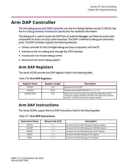
Arm DAP ControllerThe Arm debug access port (DAP) controller uses the Arm debug interface version 5 (ADIv5). See the Arm Debug Interface Architecture Specification for additional information.The debug port is used to access the DAP from an external debugger, and there are access port components to access on-chip system resources. The DAP is referred to debug port and access ports. The DAP controller supports the following features:•Central controller for the CoreSight debug and trace components with the PS•Interface to the Arm debug tools through the JTAG interface•Invasive and non-invasive debug control•Secure and non-secure debug supportArm DAP RegistersThe Versal ACAPs provide Arm DAP registers listed in the following table.Table 270: Arm DAP RegistersRegister Name Register Length DescriptionBYPASS1-bit Bypasses the Arm DAPIDCODE32-bit Captures the Arm DAP IDCODE (6BA00477h)INSTRUCTION4-bit Holds the current instruction opcode. The total Versal ACAPinstruction register length is the DAP (4-bit instruction registerlength) + TAP (6-bit instruction register length).Arm DAP InstructionsThe Versal ACAPs support the Arm DAP instructions listed in the following table.Table 271: Arm DAP InstructionsInstruction Name Binary Code [3:0]DescriptionBYPASS1111Accesses the Arm JTAG debug port Bypass registerIDCODE1110Accesses the Arm JTAG debug port IDCODE registerABORT1000Accesses the Arm JTAG debug port Abort registerDPACC1010Accesses the JTAG debug port DP registerAPACC1011Accesses the JTAG debug port AP registerHigh-Speed Debug PortThe high-speed debug port (HSDP) is a protocol that provides a unified debug and tracecapability for programmable logic, processing system, and the AI Engines. The HSDP leveragesgigabit transceivers from various sources in the device to make debug less intrusive to the system configuration.The HSDP debug packet controller (DPC) can be accessed by the host through a high-speedcable or PCIe to perform high-speed transactions on behalf of the host. The solution alsosupports at-speed debug of PL designs through ChipScope™.The HSDP has two layers, a transaction layer and a link layer. The PMC DPC is the transactionlayer that processes the packets. The link layer is the interface to communicate to the DPC, with four options as shown in the following table.Table 272: DPC Link Layer OptionsInterface Description ComparisonHSDP Aurora (hard IP)Aurora hardened interface access via gigabittransceivers Preferred choice when available. Uses HSDP with gigabit transceivers, enabling the maximum frequency and adds the capability to daisy-chain multiple Versal devices for debugging multiple devices on the same board.Debug CPM PCIe PCIe interface access via XPIPE, gigabittransceivers, and CPM PCIe block Can be chosen when a gigabit transceiver is also needed for maximum PCIe throughput. Transmits DPC packets over PCIe protocol.PL Aurora (soft IP)PL fabric interface access via AXI4-Stream into PLto enable soft Aurora Can be selected when no other choice is available. Can also be considered an HSDP if full protocol is implemented. DPC access is available after the PL design has been loaded.JTAG JTAG IEEE 1149.1 standard interface Limited to the maximum JTAG interfacefrequency (see Versal ACAP data sheets). The packets processed by DPC are referred to as debug and trace packets (DTP). Each packet consists of a header, payload, and CRC fields. The DPC decodes the payloads to determine the commands, destinations, and any required higher level flow control and management tasks. DPC processes the DTP sent by a host, executes commands embedded in them and generates responses including errors sent back to the host.Host Debug PortsThe following figure provides a view of the JTAG and HSDP interfaces.Section XV: Test and DebugChapter 80: Integrated DebugFigure 116: Host Debug Port InterfacesX22479-112320Debug Packet ControllerThe debug packet controller (DPC) is included in the PMC. The DPC is the central part of the high-speed debug port solution (HSDP). The HSDP defined protocol is separated into two layers, the transaction layer with the DPC and the link layer with Aurora or PL if exactly the same protocol is supported. The non-HSDP link layer is supported with JTAG or PL. The DPC receives and executes input packets from one of the supported interfaces. The DPC then generates reply packets and transmits them to the interface. The DPC is divided into the following blocks:•FIFO captures the input stream from AXI•De-multiplexer and decode identifies the packet boundaries and decodes non-queued and queued packets•Command buffers to buffer the queued command packets•Processing engine to process the queued packets and interfaces with the external switch •Reply buffers generate reply packets that are waiting to be transmitted to the output to the AXI。
FPGA可编程逻辑器件芯片XC3S200-4FG320C中文规格书

Revision HistoryThe following table shows the revision history for this document.Date Version Revision04/04/2018 4.4•All new “GT Locations” appendix.•Added Integrated Debug Options to “Debugging” appendix.12/20/2017 4.4•Removed documented support for Resizable BAR (RBAR).In Chapter 2, “Product Specification”:•Added details about phy_rdy_output signal in Clock and Reset Interfacesection.In Chapter 3, “Designing with the Core”:•Added note regarding configuration bank 65 in the Tandem Configurationsection.•Updated the Legacy Interrupt Signaling figure and description.10/04/2017 4.4In Chapter 1, “Overview”:•Updated Table 2-1: Available Integrated Block for PCI Express.In Chapter 2, “Product Specification”:•Updated the documented cfg_mgmt_addr width.•Minor updates to description for cfg_current_speed, cfg_max_payload,cfg_max_read_req, cfg_err_cor_out, cfg_err_nonfatal_out, cfg_err_fatal_out,cfg_local_error.•Major updates to description for cfg_interrupt_msi_function_number,cfg_ext_read_data_valid.In Chapter 3, “Designing with the Core”:•Updated the Tandem Configuration section.•Major updates to description for Completer Completion Descriptor FieldsBit Indexes 79:72, 87:80, and 88.•Major updates to description for Requester Request Descriptor Fields BitIndexes 87:80, 95:88, and 120.In Chapter 4, “Design Flow Steps”:•Added further details to the following Vivado IP catalog option:°PF0 ID Initial Values > Device ID value (in Identity Setting (PF0 IDs andPF1 IDs) tab).°MSIx Table Settings > Table Size (in MSI-X Capabilities tab).In Appendix A, “Upgrading”:•Updated Port and Parameters changes for the current core version.New Appendix D, “Using Xilinx Virtual Cable to Debug.”06/07/2017 4.3•Minor updates to the Tandem Configuration section.•Updated port description for cfg_interrupt_msi_pending_status.•Updated MSI Mode figure.04/05/2017 4.3In Chapter 3, “Designing with the Core”:•Added the GT Wizard option to the Shared Logic section.•Updated the Tandem Configuration section.In Chapter 4, “Design Flow Steps”:•Added PCIe DRP Ports and GT DRP Ports tables.•Added support for Gen1 and Gen2 speed links to the Enable In SystemIBERT option.12/19/2016 4.2•In Chapter 4, “Design Flow Steps”, clarified that the Enable In System IBERToption should be used only for hardware debugging. Simulations are notsupported for the cores generated using these options.11/30/2016 4.2Vivado IP catalog core option changes:•Added ECRC check capable sub option to the Enable AER Capability optionin the Extended Capabilities 1 and Extended Capabilities 2 tab.•Clarified the effect of Enable Auto RxEq setting on the LPM or DFE settingin the GT Settings tab.10/19/2016 4.2•Editorial updates in Chapter 2, “Product Specification”.10/05/2016 4.2•Moved the performance and resource utilization data to the web.•Updated the Tandem Configuration section.•Updated the BAR Size Ranges for Device Configuration table in the DesignFlow Steps chapter.•Added the Enable Parity option to the Basic tab (Advanced Mode), theEnable Auto RxEq option to the GT Settings tab, and added the Enable InSystem IBERT, Enable Descrambler for Gen3 Mode, and Enable JTAGDebugger parameters in the new Add. Debug Options tab in the DesignFlow Steps chapter.•Updated the Parameter Changes table and Ports Changes table in theMigrating and Updating appendix.06/08/2016 4.2•Updated Tandem Configuration section•Updated Generating Interrupt Requests•New device GT locations added.04/06/2016 4.2•In the Tandem Configuration section:°Updated the Tandem PROM/PCIe Support Configurations table.°Added the Tandem with Field Updates section.°Added the Debugging Tandem with Field Updates Designs section.•Added new Parameters Changes and Ports Changes table to the Migratingand Updating appendix.•Updated the Kintex UltraScale Device GT Locations table.01/29/2016 4.1•Updated Table: 2-2 Available Integrated Blocks for PCI Express.11/20/2015 4.1•Updated details for Gen3 in Table 2-3: Minimum Device Requirements.11/18/2015 4.1•Added the FFVA1156 package to the XCKU095 device in the AvailableIntegrated Blocks For PCI Express table (Chapter 2), and Kintex®UltraScale™ Device GT Locations table (Appendix B).•Updated the supported speed grades.•Updated the width for the following ports: cfg_function_status,cfg_vf_status, cfg_function_power_state, cfg_vf_power_state, cfg_rcb_status,cfg_dpa_substate_change, cfg_tph_requester_enable, cfg_tph_st_mode,cfg_vf_tph_requester_enable, cfg_vf_tph_st_mode, cfg_vf_flr_in_process,cfg_per_function_number, cfg_flr_done, cfg_flr_in_process,cfg_interrupt_pending, cfg_interrupt_msi_enable, cfg_interrupt_msi_vf_enable,and cfg_interrupt_msi_mmenable.•Added available negotiated link width values for cfg_negotiated_width.•Updated the status (Not Supported, Beta, Production) in the TandemPROM/PCIe Supported Configurations table.•Removed the Message Signal Interrupt option from the Vivado IDE.•Added the Enable RX Message INTFC option to the Vivado IDE.09/30/2015 4.1•Updated the available integrated blocks for PCIe.•Updated the Tandem Configuration section.•Updated PIPE signal mapping tables: Common In/Out Commands andEndpoint PIPE Signals Mappings, and Input/Output Bus with Endpoint PIPESignals Mapping.•Updated the recommended Virtex® UltraScale device, and KintexUltraScale device GT locations.07/02/2015 4.0•Corrected resource utilization data.06/24/2015 4.0•Updated the available integrated blocks for PCI Express.•Added the Minimum Device Requirements table.•Updated the documented m_axis_cq_tdata signal width.•Updated the signal description for addr_offset[2:0].•Added the sys_clk_gt signal.•Updated the Common PCI Configuration Space Header table.•Updated the USER_CLK2_FREQ attribute values.•Added an Important note regarding when Shared Logic is available.•Updated the Tandem Configuration section.•Added the Receive Ordering Rules table (Receive Transaction Orderingsection).•Added the Relocating the Integrated Block Core section.•GT locations:°Renamed core pinouts to GT locations throughout.°Added command to print specific package pins for a GT location.°Updated the Recommended Virtex UltraScale GT Locations table.05/07/2015 4.0•Updated the Tandem Configuration section.。
FPGA可编程逻辑器件芯片XC3S200A-4FGG320I中文规格书
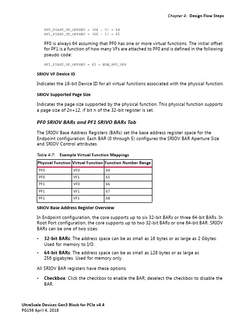
UltraScale Devices Gen3 Block for PCIe v4.4PG156 April 4, 2018Chapter 4:Design Flow StepsPF0_FIRST_VF_OFFSET = (64 - 0) = 64PF1_FIRST_VF_OFFSET = (66 - 1) = 65PF0 is always 64 assuming that PF0 has one or more virtual functions. The initial offset for PF1 is a function of how many VFs are attached to PF0 and is defined in the following pseudo code:PF1_FIRST_VF_OFFSET = 63 + NUM_PF0_VFSSRIOV VF Device IDIndicates the 16-bit Device ID for all virtual functions associated with the physical function.SRIOV Supported Page SizeIndicates the page size supported by the physical function. This physical function supports a page size of 2n+12, if bit n of the 32-bit register is set.PF0 SRIOV BARs and PF1 SRIVO BARs TabThe SRIOV Base Address Registers (BARs) set the base address register space for the Endpoint configuration. Each BAR (0 through 5) configures the SRIOV BAR Aperture Size and SRIOV Control attributes.SRIOV Base Address Register OverviewIn Endpoint configuration, the core supports up to six 32-bit BARs or three 64-bit BARs. In Root Port configuration, the core supports up to two 32-bit BARs or one 64-bit BAR. SRIOV BARs can be one of two sizes:•32-bit BARs : The address space can be as small as 16 bytes or as large as 2 ed for memory to I/O.•64-bit BARs : The address space can be as small as 128 bytes or as large as 256 gigabytes. Used for memory only.All SRIOV BAR registers have these options:•Checkbox : Click the checkbox to enable the BAR; deselect the checkbox to disable the BAR.Table 4-7:Example Virtual Function Mappings Physical Function Virtual Function Function Number RangePF0VF064PF0VF165PF1VF066PF1VF167PF1VF168UltraScale Devices Gen3 Block for PCIe v4.4PG156 April 4, 2018Chapter 4:Design Flow Steps•Type : SRIOV BARs can either be I/O or Memory.°I/O : I/O BARs can only be 32-bit; the Prefetchable option does not apply to I/O BARs. I/O BARs are only enabled for the Legacy PCI Express Endpoint core.°Memory : Memory BARs can be either 64-bit or 32-bit and can be prefetchable.When a BAR is set as 64 bits, it uses the next BAR for the extended address space and makes the next BAR inaccessible.•Size : The available size range depends on the PCIe device/port type and the type of BAR selected. Table 4-8 lists the available BAR size ranges.•Prefetchable : Identifies the ability of the memory space to be prefetched.•Value : The value assigned to the BAR based on the current selections.For more information about managing the SRIOV Base Address Register settings, see Managing Base Address Register Settings .Managing SRIOV Base Address Register SettingsMemory, I/O, Type, and Prefetchable settings are handled by setting the appropriate Customize IP dialog box settings for the desired base address register.Memory or I/O settings indicate whether the address space is defined as memory or I/O. The base address register only responds to commands that access the specified address space. Generally, memory spaces less than 4 KB in size should be avoided. The minimum I/O space allowed is 16 bytes. I/O space should be avoided in all new designs.A memory space is prefetchable if there are no side effects on reads (that is, data is not destroyed by reading, as from RAM). Byte-write operations can be merged into a single double-word write, when applicable.When configuring the core as an Endpoint for PCIe (non-Legacy), 64-bit addressing must be supported for all SRIOV BARs (except BAR5) that have the prefetchable bit set. 32-bit addressing is permitted for all SRIOV BARs that do not have the prefetchable bit set. The prefetchable bit related requirement does not apply to a Legacy Endpoint. The minimum memory address range supported by a BAR is 128 bytes for a PCI Express Endpoint and 16 bytes for a Legacy PCI Express Endpoint.Table 4-8:SRIOV BAR Size Ranges for Device Configuration PCIe Device / Port Type BAR TypeBAR Size Range PCI Express Endpoint 32-bit Memory128 bytes – 2 gigabytes 64-bit Memory128 bytes – 256 gigabytes Legacy PCI Express Endpoint 32-bit Memory16 bytes – 2 gigabytes 64-bit Memory16 bytes – 256 gigabytes I/O 16 bytes – 2 gigabytesUltraScale Devices Gen3 Block for PCIe v4.4 PG156 April 4, 2018Chapter 4:Design Flow StepsDisabling Unused ResourcesFor best results, disable unused base address registers to conserve system resources. Disable base address register by deselecting unused BARs in the Customize IP dialog box.Legacy/MSI Capabilities TabThis page is the same as that of Basic mode.MSI-X Capabilities TabThe MSI-X Capabilities parameters are available in Advanced mode only.Enable MSIx Capability StructureIndicates that the MSI-X Capability structure exists.Note:The Capability Structure needs at least one Memory BAR to be configured. You must maintain the MSI-X Table and Pending Bit Array in the application.MSIx Table Settings:Defines the MSI-X Table structure.•Table Size: Specifies the MSI-X Table size. Table Size field is expecting N-1 interrupts (0x0F will configure a table count of 16).•Table Offset: Specifies the offset from the Base Address Register that points to the base of the MSI-X Table.•BAR Indicator: Indicates the Base Address Register in the Configuration Space used to map the function in the MSI-X Table onto memory space. For a 64-bit Base Address Register, this indicates the lower DWORD.MSIx Pending Bit Array (PBA) SettingsDefines the MSI-X Pending Bit Array (PBA) structure.•PBA Offset: Specifies the offset from the Base Address Register that points to the base of the MSI-X PBA.•PBA BAR Indicator: Indicates the Base Address Register in the Configuration Space used to map the function in the MSI-X PBA onto Memory Space.Power ManagementThe Power Management page includes settings for the Power Management registers, power consumption, and power dissipation options. These settings apply to both physical functions, if PF1 is enabled.。
FPGA可编程逻辑器件芯片XC3S200A-4FG320C中文规格书
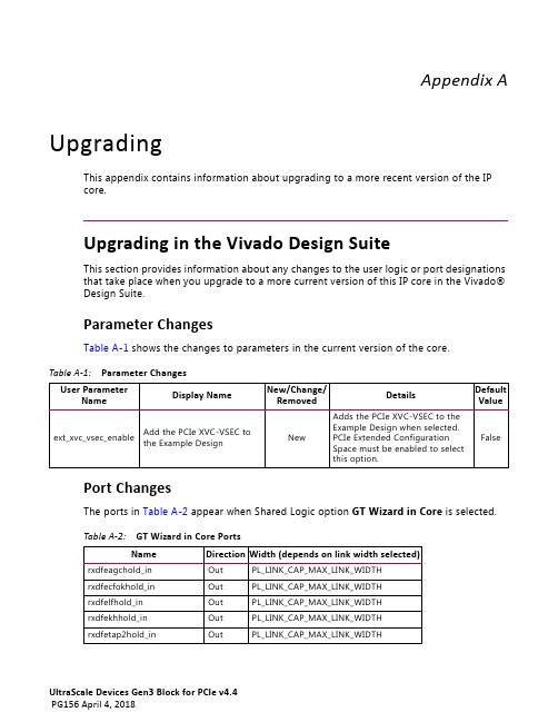
Appendix AUpgradingThis appendix contains information about upgrading to a more recent version of the IP core.Upgrading in the Vivado Design SuiteThis section provides information about any changes to the user logic or port designations that take place when you upgrade to a more current version of this IP core in the Vivado® Design Suite.Parameter ChangesTable A-1 shows the changes to parameters in the current version of the core.Port ChangesThe ports in Table A-2 appear when Shared Logic option GT Wizard in Core is selected. Table A-1:Parameter Changes User Parameter Name Display Name New/Change/Removed DetailsDefault Value ext_xvc_vsec_enable Add the PCIe XVC-VSEC to the Example Design New Adds the PCIe XVC-VSEC to the Example Design when selected. PCIe Extended Configuration Space must be enabled to select this option.FalseTable A-2:GT Wizard in Core Ports NameDirection Width (depends on link width selected)rxdfeagchold_inOut PL_LINK_CAP_MAX_LINK_WIDTH rxdfecfokhold_inOut PL_LINK_CAP_MAX_LINK_WIDTH rxdfelfhold_inOut PL_LINK_CAP_MAX_LINK_WIDTH rxdfekhhold_inOut PL_LINK_CAP_MAX_LINK_WIDTH rxdfetap2hold_in Out PL_LINK_CAP_MAX_LINK_WIDTHEndpoint Model Test Bench for Root PortThe Endpoint model test bench for the core in Root Port configuration is a simple example test bench that connects the Configurator example design and the PCI Express Endpoint model allowing the two to operate like two devices in a physical system. As the Configurator example design consists of logic that initializes itself and generates and consumes bus traffic, the example test bench only implements logic to monitor the operation of the system and terminate the simulation.The Endpoint model test bench consists of:•Verilog or VHDL source code for all Endpoint model components •PIO slave design TSK_EXPECT_MEMWR64traffic_classtdepattrlengthrequester_idtaglast_dw_befirst_dw_beaddress2:0--1:010:015:07:03:03:061:0Expect status Waits for a 64-bit Address Memory Write TLP with matching header fields. Returns a 1 on successful completion; 0 otherwise.This task can only be used in conjunction with Bus Master designs.TSK_EXPECT_IOWR tdeprequester_idtagfirst_dw_beaddressdata --15:07:03:031:031:0Expect status Waits for an I/O Write TLP with matching header fields. Returns a 1 on successful completion; 0 otherwise.This task can only be used in conjunction with Bus Master designs.Table 6-6:Expectation Tasks (Cont’d)Name Input(s)Output DescriptionFigure6-1 illustrates the Endpoint model coupled with the Configurator example design.ArchitectureThe Endpoint model consists of these blocks:•PCI Express Endpoint (the core in Endpoint configuration) model.•PIO slave design, consisting of:°PIO_RX_ENGINE°PIO_TX_ENGINE°PIO_EP_MEM°PIO_TO_CTRLThe PIO_RX_ENGINE and PIO_TX_ENGINE blocks interface with the ep block for reception and transmission of TLPs from/to the Root Port Design Under Test (DUT). The Root Port DUT consists of the core configured as a Root Port and the Configurator Example Design, which consists of a Configurator block and a PIO Master design, or customer design.The PIO slave design is described in detail in Programmed Input/Output: Endpoint Example Design.Simulating the DesignA simulation script file ,simulate_mti.do, is provided with the model to facilitate simulation with the Mentor Graphics QuestaSim simulator.The example simulation script files are located in this directory:<project_dir>/<component_name>/simulation/functionalInstructions for simulating the Configurator example design with the Endpoint model are provided in Simulation in Chapter4.Note:For Cadence IES users, the work construct must be manually inserted into the cds.lib file: DEFINE WORK WORK.Scaled Simulation TimeoutsThe simulation model of the core uses scaled down times during link training to allow for the link to train in a reasonable amount of time during simulation. According to the PCI Express Specification, rev. 3.0 [Ref2], there are various timeouts associated with the link training and status state machine (LTSSM) states. The core scales these timeouts by a factor of 256 in simulation, except in the Recovery Speed_1 LTSSM state, where the timeouts are not scaled.。
FPGA可编程逻辑器件芯片XC3S200-4CPG132C中文规格书

Figure 95: IrDA SIR ENDEC Block DiagramX24307-073020Transmit EncoderThe SIR transmit encoder modulates the non return-to-zero (NRZ) transmit bit stream output from the UART. The IrDA SIR physical layer specifies the use of a return to zero, inverted (RZI) modulation scheme that represents logic 0 as an infrared light pulse. The modulated output pulse stream is transmitted to an external output driver and infrared light emitting diode (LED).The frequency of IrLPBaud16 is set up by writing the appropriate divisor value to the IrDA Low Power Counter register, UART.IR_LOWPR.The active-Low encoder output is normally Low for the marking state (no light pulse). The encoder outputs a high pulse to generate an infrared light pulse representing a logic 0 or spacing state.Receive DecoderThe SIR receive decoder demodulates the return-to-zero bitstream from the infrared detector and outputs the received NRZ serial bitstream to the UART received data input. The decoder input is normally High (marking state) in the idle state. The transmit encoder output has the opposite polarity to the decoder input.A start bit is detected when the decoder input is Low.Note: T o prevent the UART from responding to glitches on the received data input then it ignores SIRIN pulses that are less than:•3/16 of Baud16, in IrDA mode•3/16 of IrLPBaud16, in low-power IrDA modeData ModulationThe following figure shows the IrDA data modulation.Figure 96: UART IrDA 3/16 Data ModulationInterruptsEleven maskable interrupts are generated in the UART. These are combined to produce onesystem interrupt that is the OR of the individual outputs. Interrupts can be enabled or disabled individually by changing the mask bits in the interrupt mask set/clear register, INTR_IMSC.Setting the appropriate mask bit High enables the interrupt.Flow Control InterruptsThe modem status interrupt is asserted if any of the modem status signals (UARTx_CTS_b,DCD_b, DSR_b, and RI_b) change. It is cleared by writing a 1 to the corresponding bits in the Interrupt Clear register, INTR_CLR , depending on the modem status signals that generated the interrupt.Change State InterruptThe transmit interrupt changes state when one of the following events occurs:•If the FIFOs are enabled and the transmit FIFO is equal to or lower than the programmed trigger level, the transmit interrupt is asserted High. The transmit interrupt is cleared bywriting data to the transmit FIFO until it becomes greater than the trigger level, or by clearing the interrupt.•If the FIFOs are disabled (have a depth of one location) and there is no data present in the transmitters single location, the transmit interrupt is asserted High. It is cleared by performing a single write to the transmit FIFO, or by clearing the interrupt.•T o update the transmit FIFO, write data to the transmit FIFO, either prior to enabling the UART and the interrupts, or after enabling the UART and interrupts.Note : The transmit interrupt is based on a transition through a level, rather than on the level itself. When the interrupt and the UART is enabled before any data is written to the transmit FIFO the interrupt is not set. The interrupt is only set, after written data leaves the single location of the transmit FIFO and it becomes empty.Timeout InterruptThe receive timeout interrupt is asserted when the receive FIFO is not empty and no more data is received during a 32-bit period. The receive timeout interrupt is cleared either when the FIFO becomes empty through reading all the data (or by reading the holding register), or when a 1 is written to the corresponding bit of the Interrupt Clear register, INTR_CLR .Error InterruptThe error interrupt is asserted when an error occurs in the reception of data by the UART. The interrupt can be caused by a number of different error conditions:•Framing•Parity•Break•OverrunSection XII: I/O Peripheral ControllersChapter 71: UART SBSA Controller。
FPGA可编程逻辑器件芯片XC3S200A-5FTG256I中文规格书
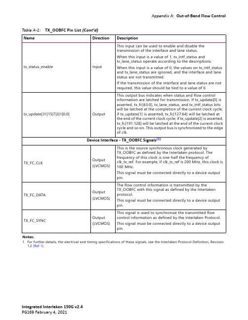
tx_status_enable Input This input can be used to enable and disable the transmission of the interface and lane status.When this input is a value of 1, tx_intf_status and tx_lane_status operate according to the descriptions.When this input is a value of 0, the values on tx_intf_status and tx_lane_status are ignored, and the interface and lane status are not transmitted.If the transmission of the interface and lane status are not required, this value should be tied to a value of 0.tx_update[31|15|7|3|1|0:0]OutputThis output bus indicates when status and flow control information are latched for transmission. If tx_update[0] is asserted, tx_fc[63:0], tx_lane_status, and tx_intf_status bits will be latched at the completion of the current clock cycle; if tx_update[1] is asserted, tx_fc[127:64] will be latched at the end of the current clock cycle; if tx_update[2] is asserted, tx_fc[191:128] will be latched at the end of the current clock cycle and so on. This output bus is synchronized to the edge of clk.Device Interface - TX_OOBFC Signals (1)TX_FC_CLK Output (LVCMOS)This is the source synchronous clock generated by TX_OOBFC as defined by the Interlaken protocol. The frequency of this clock is one-half the frequency of clk_tx_ref. For example, if clk_tx_ref is 200 MHz, this clock is 100 MHz.This signal must be connected directly to a device output pin.TX_FC_DATA Output(LVCMOS)The flow control information is transmitted by the TX_OOBFC with this signal as defined by the Interlaken protocol.This signal must be connected directly to a device output pin.TX_FC_SYNC Output (LVCMOS)This signal is used to synchronize the transmitted flow control information as defined by the Interlaken Protocol.This signal must be connected directly to a device output pin.Notes:1.For further details, the electrical and timing specifications of these signals, see the Interlaken Protocol Definition, Revision 1.2 [Ref 1].Table A-1:TX_OOBFC Pin List (Cont’d)Name Direction DescriptionTable A-2:RX_OOBFC Pin ListName Direction DescriptionClocking and Resetsclk Input All signals between the RX_OOBFC and the user logic are synchronized to the positive edge of clk. In typical applications, this clock should be tied to the same clock used to run the user-side interface of the Interlaken Core. In order for correct operation in the RX_OOBFC, the frequency of this clock must be at least 33% faster than the frequency of RX_FC_CLK. For example, if the frequency of RX_FC_CLK is 100 MHz, the frequency of clk must be at least 133 MHz.reset Input Active-High, asynchronous reset input. This signal is automatically synchronized to the appropriate clock domain by the RX_OOBFC. All circuits in the module are reset while this input is a value of 1. This signal must remain asserted until after several clock cycles on both the clk and RX_FC_CLK inputs.User-Side Interface - RX_OOBFC Signalsrx_fc[MAX_CAL-1:0]Output Output data bus to the user logic containing the flow control information received by the RX_OOBFC. The width of the bus is set by the MAX_CAL parameter. Bit 0 corresponds to channel 0, bit 1 corresponds to channel 1, and so on. Interlaken defines a value of 1 as XON and a value of 0 as XOFF.If the calendar length for the received flow control information has less than MAX_CAL entries, the unused bits are undefined and should be ignored. It is up to you to monitor this bus and take appropriate action as flow control information is changed. When an unhealthy interface status is received, as indicated by rx_intf_status being a value of 0, or an unhealthy lane status is received, as indicated by a bit of rx_lane_status being a value of 0, then all bits of rx_fc are XOFF or a value of 0.When a CRC error is detected, the outputs rx_fc are unchanged. This bus is synchronized to the positive edge of clk.rx_crcerr Output Indicates if an error was observed in the CRC field of the incoming status or flow control information. A value of 1 indicates a CRC error was detected. When this bit is a value of 1, the outputs rx_fc, rx_intf_status, and rx_lane_status are not updated and can be ignored. The cause of a CRC error can be due to clk not being sufficiently faster than RX_FC_CLK as required for correct operation.This signal is synchronized to the positive edge of clk.rx_overflow Output Indicates that clk is not faster than RX_FC_CLK as required for correct operation.This signal is synchronized to the positive edge of clk.rx_intf_status Output Indicates the health of the receive interface as described in the Interlaken specification. When this output has a value of 0, all flow-control bits in the rx_fc bus will be XOFF (that is, 0).This signal is synchronized to the positive edge of clk.Appendix A:Out-of-Band Flow Control rx_lane_status[11:0]Output Indicates the health of the corresponding receive lanes as described in the Interlaken specification. Bit 0 corresponds to lane 0, bit 1 corresponds to lane 1, and so on. When any bit of this bus has a value of 0, all flow-control bits in the rx_fc bus will be XOFF (that is, 0).This bus is synchronized to the positive edge of clk.rx_update [31|15|7|3|1|0:0]Output Indicates a valid CRC4 was detected and rx_fc bits were updated. If rx_update[0] is asserted, the CRC4 associated with rx_fc[63:0] was valid and rx_fc[63:0] were updated; if rx_update[1] is asserted, the CRC4 associated with rx_fc[127:64] was valid and rx_fc[127:64] were updated, and so on. This bus is synchronized to the positive edge of clk.rx_callen_minus1[10|9|8|7:0]Output Indicates the length of the most recently received calendar. This bus is synchronized to the positive edge of clk.rx_force_xoff_if_crcerr InputWhen this input is a value of 1, all bits of rx_fc are forced to XOFF if a CRC error is detected.Device Interface - RX_OOBFC Signals (1)RX_FC_CLK Input(LVCMOS)This the source-synchronous clock used by RX_OOBFC as defined by the Interlaken protocol.This signal must be connected directly to a device input pin.RX_FC_DATA Input(LVCMOS)The flow control information is received by the RX_OOBFC with this signal as defined by the Interlaken protocol.This signal must be connected directly to a device input pin.RX_FC_SYNCInput(LVCMOS)This signal is used to synchronize the received flow control information as defined by the Interlaken Protocol.This signal must be connected directly to a device input pin.Notes:1.Further details of the electrical and timing specifications for these signals are found in the Interlaken Protocol Definition,Revision 1.2 [Ref 1].Table A-2:RX_OOBFC Pin List (Cont’d)Name Direction Description。
FPGA可编程逻辑器件芯片XC3S200-5FG900C中文规格书
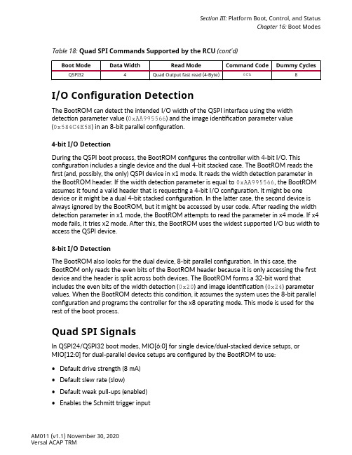
Table 18: Quad SPI Commands Supported by the RCU (cont'd)Boot Mode Data Width Read Mode Command Code Dummy Cycles QSPI324Quad Output fast read (4-Byte)6Ch8I/O Configuration DetectionThe BootROM can detect the intended I/O width of the QSPI interface using the width detection parameter value (0xAA995566) and the image identification parameter value(0x584C4E58) in an 8-bit parallel configuration.4-bit I/O DetectionDuring the QSPI boot process, the BootROM configures the controller with 4-bit I/O. This configuration includes a single device and the dual 4-bit stacked case. The BootROM reads the first (and, possibly, the only) QSPI device in x1 mode. It reads the width detection parameter in the BootROM header. If the width detection parameter is equal to 0xAA995566, the BootROM assumes it found a valid header that is requesting a 4-bit I/O configuration. It might be one device or it might be a dual 4-bit stacked configuration. In the latter case, the second device is always ignored by the BootROM, but it might be accessed by user code. After reading the width detection parameter in x1 mode, the BootROM attempts to read the parameter in x4 mode. If x4 mode fails, it tries x2 mode. After this, the BootROM uses the widest supported I/O bus width to access the QSPI device.8-bit I/O DetectionThe BootROM also looks for the dual device, 8-bit parallel configuration. In this case, the BootROM only reads the even bits of the BootROM header because it is only accessing the first device and the header is split across both devices. The BootROM forms a 32-bit word that includes the even bits of the width detection (0x20) and image identification (0x24) parameter values. When the BootROM detects this condition, it assumes the system uses the 8-bit parallel configuration and programs the controller for the x8 operating mode. This mode is used for the rest of the boot process.Quad SPI SignalsIn QSPI24/QSPI32 boot modes, MIO[6:0] for single device/dual-stacked device setups, orMIO[12:0] for dual-parallel device setups are configured by the BootROM to use:•Default drive strength (8 mA)•Default slew rate (slow)•Default weak pull-ups (enabled)•Enables the Schmitt trigger input•Disables the 3-state overrideThe remaining MIOs are not set by the BootROM and remain at their default state. If a secure lockdown occurs during boot, the BootROM sets the to 0xFFFF_FFFF to 3-state all I/Os. See Versal ACAP Register Reference (AM012) for details.The following table lists the bidirectional PMC multiplexed I/Os (MIOs) and their functions used in the Quad SPI boot mode setup.Table 19: Quad SPI Boot Mode SignalsPMC MIO Pin Signal Name Description0QSPI0_CLK QSPI0 clock output4QSPI0_IO[0]I/O pin used as MOSI in 1-bit modeI/O pin used as the lower QSPI0_IO[0] in 2-bit or 4-bit single or dual-stacked setups, and in 8-bit dual-parallel setups1QSPI0_IO[1]I/O pin used as MISO in 1-bit modeI/O pin used as the lower QSPI0_IO[1] in 2-bit or 4-bit single or dual-stacked setups, and in 8-bit dual-parallel setups2QSPI0_IO[2]I/O pin used as the lower QSPI0_IO[2] in 4-bit single or dual-stacked setups, and in 8-bit dual-parallel setups3QSPI0_IO[3]I/O pin used as the lower QSPI0_IO[3] in 4-bit single or dual-stacked setups, and in 8-bit dual-parallel setups5QSPI0_CS_b Active-Low chip select output that enables QSPI0 (lower) flash device12QSPI1_CLK QSPI1 clock output8QSPI1_IO[0]I/O pin used as MOSI in 1-bit modeI/O pin used as the upper QSPI1_IO[0] in 2-bit or 4-bit dual-stacked setups, and in 8-bit dual-parallel setups9QSPI1_IO[1]I/O pin used as MISO in 1-bit modeI/O pin used as the upper QSPI1_IO[1] in 2-bit or 4-bit dual-stacked setups, and in 8-bit dual-parallel setup10QSPI1_IO[2]I/O pin used as the upper QSPI1_IO[2] in 4-bit dual-stacked setups, and in 8-bit dual-parallel setups11QSPI1_IO[3]I/O pin used as the upper QSPI1_IO[3] in 4-bit dual-stacked setups, and in 8-bit dual-parallel setups7QSPI1_CS_b Active-Low chip select output enables QSPI1 (upper) flash device6QSPI_LPBK_CLK I/O pin used for loopback clockThe loopback clock is an internal clock signal that is routed through the output buffer to this pin and returned back through the pin's input buffer to the quad SPI controller for I/O delay compensation.When the quad SPI device clock frequency is >37.5 MHz, the loopback clock must be enabled in the CIPS IP core and must be left connected on the board.When the quad SPI device clock frequency ≤37.5 MHz, the loopback clock should be disabled so MIO[6] is not used by the quad SPI controller and it can be used as another peripheral I/O.Single Device InterfaceThe QSPI single-device mode is a common setup because it is low cost and has a lower pin count boot and configuration option. The QSPI single-device mode supports 1-bit, 2-bit, and 4-bit bus widths. This mode also supports 24-bit addressing and 32-bit addressing modes.An example QSPI interface setup for a 4-bit bus width and 32-bit addressing mode is shown in the following figure.Figure 20: Quad SPI Single Device InterfaceNote : For QSPI0_CLK >37.5 MHz, QSPI_LPBK_CLK must be enabled in the design and left unconnected on the board.X22624-102020The following figure shows an example QSPI read waveform with the relative sequence of events.Figure 21: QSPI Example Read WaveformDual-Stacked InterfaceTwo QSPI devices share the same bus in QSPI dual-stacked mode to double the maximumaddressable flash memory storage for the application. This mode also reduces the boot interface I/O pin count because the bus is shared and only one additional interface pin is needed for the flash select. In this mode, only the lower QSPI addressable flash memory space can be used for boot and the throughput remains the same as it is in the QSPI single-device mode.Section III: Platform Boot, Control, and StatusChapter 16: Boot Modes。
FPGA可编程逻辑器件芯片XC3S200A-5FTG256C中文规格书

Chapter 2:Product SpecificationXCKU115FLVA1517Yes Yes Yes Yes Yes Yes(2) FLVB1760Yes Yes Yes Yes Yes Yes FLVF1924Yes Yes Yes Yes Yes Yes FLVD1924Yes Yes Yes(2)Yes Yes Yes FLVD1517Yes Yes Yes Yes Yes Yes FLVA2104Yes Yes Yes Yes Yes Yes FLVB2104Yes Yes Yes Yes Yes YesXQKU115RLD1517Yes Yes Yes Yes Yes Yes RLF1924Yes Yes Yes Yes Yes YesXCVU065FFVC1517Yes YesXCVU080FFVA2104Yes Yes Yes Yes FFVB2104Yes Yes Yes Yes FFVB1760Yes Yes Yes Yes FFVC1517Yes Yes Yes Yes(2) FFVD1517Yes Yes Yes YesXCVU095FFVA2104Yes Yes Yes Yes FFVB2104Yes Yes Yes Yes FFVB1760Yes Yes Yes Yes FFVC2104Yes Yes Yes Yes FFVC1517Yes Yes Yes Yes(2) FFVD1517Yes Yes Yes YesXCVU125FLVB1760Yes Yes Yes Yes FLVB2104Yes Yes Yes Yes FLVC2104Yes Yes Yes Yes FLVA2104Yes Yes Yes Yes FLVD1517Yes Yes Yes YesXCVU160FLGB2104Yes Yes Yes Yes FLGC2104(1)Yes Yes Yes Yes YesXCVU190FLGB2104Yes Yes Yes Yes FLGC2104Yes Yes Yes Yes Yes Yes FLGA2577Yes Yes Yes Yes Yes YesTable 2-2:Available Integrated Blocks for PCI Express (Cont’d)Device Selection PCI Express Block Location Device Package X0Y0X0Y1X0Y2X0Y3X0Y4X0Y5GT LocationsThe recommended GT locations for the available device part and package combinations are available in Appendix B, GT Locations . The package pins are derived directly from the GT X-Y locations listed in the appendix. The Vivado Design Suite provides an XDC for the selected part and package that matches the contents of the tables.•Virtex UltraScale Devices Available GT Quads •Kintex UltraScale Devices Available GT QuadsPort DescriptionsThis section provides detailed port descriptions for the following interfaces:•AXI4-Stream Core Interfaces •Other Core InterfacesAXI4-Stream Core Interfaces64/128/256-Bit InterfacesIn addition to status and control interfaces, the core has four required AXI4-Stream interfaces used to transfer and receive transactions, which are described in this pleter Request InterfaceThe Completer Request (CQ) interface are the ports through which all received requests from the link are delivered to the user application. Table 2-3 defines the ports in the CQ XCVU440FLGA2892Yes Yes Yes Yes Yes Yes FLGB2377Yes YesYes Yes Yes Yes Notes:1.The software supports only two PCIe blocks for XCKU035 devices (for non SFVA784 packages), four PCIe blocks for XCKU085 devices, and four PCIe blocks for XCVU160/FLGC2104 devices.2.Available only when the device/package migration option Enable GT Quad selection is selected. See Package Migration of UltraScale Devices PCI Express Designs .Table 2-2:Available Integrated Blocks for PCI Express (Cont’d)Device SelectionPCI Express Block Location DevicePackage X0Y0X0Y1X0Y2X0Y3X0Y4X0Y5interface of the core. In the Width column, DW denotes the configured data bus width (64, 128, or 256 bits).Table 2-3:Completer Request Interface Port DescriptionsPort Direction Width Descriptionm_axis_cq_tdata Output DW Transmit Data from the CQ Interface.Only the lower 128bits are used when the interface width is128bits, and only the lower 64 bits are used when the interface width is 64bits.Bits [255:128] are set permanently to 0 by the core when the interface width is configured as 128 bits, and bits [255:64] are set permanently to 0 when the interface width is configured as 64 bits.m_axis_cq_tuser Output85CQ User Data.This set of signals contains sideband information for the transaction layer packets (TLP) being transferred. These signals are valid when m_axis_cq_tvalid is High.Table2-4, page16 describes the individual signals in this set.m_axis_cq_tlast Output1TLAST indication for CQ Data.The core asserts this signal in the last beat of a packet to indicate the end of the packet. When a TLP is transferred in a single beat, the core sets this signal in the first beat of the transfer.m_axis_cq_tkeep Output DW/32TKEEP indication for CQ Data.The assertion of bit i of this bus during a transfer indicates to the user application that Dword i of the m_axis_cq_tdata bus contains valid data. The core sets this bit to 1 contiguously for all Dwords starting from the first Dword of the descriptor to the last Dword of the payload. Thus, m_axis_cq_tdata is set to all 1s in all beats of a packet, except in the final beat when the total size of the packet is not a multiple of the width of the data bus (in both Dwords). This is true for both Dword-aligned and address-aligned modes of payload transfer.Bits [7:4] of this bus are set permanently to 0 by the core when the interface width is configured as 128 bits, and bits [7:2] are set permanently to 0 when the interface width is configured as 64 bits.m_axis_cq_tvalid Output1CQ Data Valid.The core asserts this output whenever it is driving valid data on the m_axis_cq_tdata bus. The core keeps the valid signal asserted during the transfer of a packet. The user application can pace the data transfer using the m_axis_cq_tready signal.m_axis_cq_tready Input1CQ Data Ready.Activation of this signal by the user logic indicates to the core that the user application is ready to accept data. Data is transferred across the interface when both m_axis_cq_tvalid andm_axis_cq_tready are asserted in the same cycle.If the user application deasserts the ready signal whenm_axis_cq_tvalid is High, the core maintains the data on the bus and keeps the valid signal asserted until the user application has asserted the ready signal.。
FPGA可编程逻辑器件芯片XC3S200AN-5FT256I中文规格书
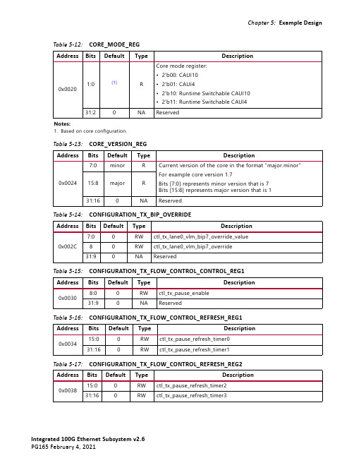
Chapter 5:Example DesignTable 5-12:CORE_MODE_REGAddress Bits Default Type Description0x00201:0(1)RCore mode register:•2'b00: CAUI10•2'b01: CAUI4•2'b10: Runtime Switchable CAUI10•2'b11: Runtime Switchable CAUI4 31:20NA ReservedNotes:1.Based on core configuration.Table 5-13:CORE_VERSION_REGAddress Bits Default Type Description0x00247:0minor R Current version of the core in the format “major.minor”For example core version 1.7Bits [7:0] represents minor version that is 7Bits [15:8] represents major version that is 115:8major R31:160NA ReservedTable 5-14:CONFIGURATION_TX_BIP_OVERRIDEAddress Bits Default Type Description0x002C 7:00RW ctl_tx_lane0_vlm_bip7_override_value 80RW ctl_tx_lane0_vlm_bip7_override 31:90NA ReservedTable 5-15:CONFIGURATION_TX_FLOW_CONTROL_CONTROL_REG1 Address Bits Default Type Description0x00308:00RW ctl_tx_pause_enable 31:90NA ReservedTable 5-16:CONFIGURATION_TX_FLOW_CONTROL_REFRESH_REG1 Address Bits Default Type Description0x003415:00RW ctl_tx_pause_refresh_timer0 31:160RW ctl_tx_pause_refresh_timer1Table 5-17:CONFIGURATION_TX_FLOW_CONTROL_REFRESH_REG2 Address Bits Default Type Description0x003815:00RW ctl_tx_pause_refresh_timer2 31:160RW ctl_tx_pause_refresh_timer3Register Descriptions 0x06A0STAT_RX_FRAGMENT 0x06A8STAT_RX_OVERSIZE 0x06B0STAT_RX_TOOLONG 0x06B8STAT_RX_JABBER 0x06C0STAT_RX_BAD_FCS 0x06C8STAT_RX_PACKET_BAD_FCS 0x06D0STAT_RX_STOMPED_FCS 0x06D8STAT_RX_UNICAST 0x06E0STAT_RX_MULTICAST 0x06E8STAT_RX_BROADCAST 0x06F0STAT_RX_VLAN 0x06F8STAT_RX_PAUSE 0x0700STAT_RX_USER_PAUSE 0x0708STAT_RX_INRANGEERR 0x0710STAT_RX_TRUNCATED 0x0718–0x07FFReserved Notes:1.Histogram/Counter registers are available when Include Statistics Counters option is selected in Figure 4-1.Table 5-7:GT_RESET_REG AddressBits Default Type Description 0x000000RW gt_reset_all. A write of 1 issues a RESET to the GT. This is a clear on write register 31:10NA ReservedTable 5-6:Status and Statistics Register Map (Cont’d)Address Register NameTable 5-8:RESET_REGAddress Bits Default Type Description0x00049:00RWusr_rx_serdes_reset. Unused PCS bits are RESERVED.A write of 1 in a given bit location puts that PCS lane logic intoreset.27:100NA Reserved280RWctl_an_reset. A write of 1, issues a reset to the Auto-Negotiationmodule. This is a clear on write register.Note:This register bit is available when 'Include AN/LTLogic' option is selected in the GUI.290NA Reserved300RW usr_rx_reset. RX core reset. A write of 1 puts the RX path in reset 310RW usr_tx_reset. TX core reset. A write of 1 puts the TX path in resetTable 5-9:SWITCH_CORE_MODE_REGAddress Bits Default Type Description0x000800RWFor Runtime Switch mode only.A write of 1 enables the mode switch between CAUI10 and CAUI4.This is a clear on write register.This is an input to the trans debug module that performs the GTDRP operations.31:10NA ReservedTable 5-10:CONFIGURATION_TX_REG1Address Bits Default Type Description0x000C00RW ctl_tx_enable3:10NA Reserved40RW ctl_tx_send_rfi50RW ctl_tx_send_idle 15:60NA Reserved160RW ctl_tx_test_pattern 31:170NA ReservedTable 5-11:CONFIGURATION_RX_REG1Address Bits Default Type Description0x001400RW ctl_rx_enable6:10NA Reserved70RW ctl_rx_force_resync 80RW ctl_rx_test_pattern 31:90NA Reserved。
- 1、下载文档前请自行甄别文档内容的完整性,平台不提供额外的编辑、内容补充、找答案等附加服务。
- 2、"仅部分预览"的文档,不可在线预览部分如存在完整性等问题,可反馈申请退款(可完整预览的文档不适用该条件!)。
- 3、如文档侵犯您的权益,请联系客服反馈,我们会尽快为您处理(人工客服工作时间:9:00-18:30)。
Lab1:Counter4.npl[实验说明] : 使用ISE9.1i设计Counter4的VHDL语法与操作说明在这一个范例中,你将开启一个counter4 的模块,与此项目所需的UCF 文件,并且利用ISE09.1i 的软件完成整个设计流程,并且将设计结果用JTAG接口连接烧录到MB_XC3S200A_FT256开发板中,验证其设计结果是否正确? 此设计同时利用ISE9.1i 的仿真功能來验证结果的正确性?.[实验目地] : 当你完成整个项目之后,你将学会以下的功能.(1).利用ISE9.1i 的软件开启一个Spartan3A FPGA 的项目.(2).撰写一个简单的VHDL 程序,利用语法检查器(Syntax Check)來修正语法的错误(3).产生测试模板(Test Pattern) 來辅助你的设计.(4).加入系统所需的Constraints 文件.(UCF file)(5).完成整个设计流程.并产生Counter4.bit 文件(6).利用FPGA Editor 來察看FPGA 内部的结果,(7).利用[Impact] 來烧录Counter4.bit 文件到FPGA.[系统需求]:PC 个人计算机ISE9.1i 软件Counter4.VHD 文件Counter4.UCF 文件Platform Cable USBXC3S200A_FT256开发板电源供应器(DC5V 输入).[操作步骤]:开启ISE9.1i软件: [程序集] → [Xilinx ISE 9.1i] → [Project Navigator] . 会出现ISE9.1i 的画面,画面开启之初, 会出现[Tip of the Day], 可以将之关掉后,出现以下的画面.(2).在ISE9.1 软件环境下,开启一个新的工程: [File] [New Project][Project Name] : Lab1_counter4[Project Location]: c: \Lab1_counter4 (依使用者设定的目录).[Top-Level Module Type] : HDL( 代表最上层的设计模块是以HDL 输方方式的模组.(3).下一个画面就是设定硬件组件的参数[FPGA系列(Device Family)]:Spartan3A( 请看板子的FPGA 组件的编号)[FPGA名称(Device)] : XC3S200A(请参考开发板的FPGA 组件的编号)[FPGA包装(Package)]:FT256(请参考开发板的FPGA 组件的编号)[FPGA速度等级(Speed)]: -4 ( FPGA 速度等级)[综合器工具(Synthesis Tool)]:XST VHDL(VHDL综合的种类)[仿真器(Simulator)] : ISE Simulator(ISE9.1 内建的仿真器)[产生仿真器的语言(Generated Simulation Language)] : VHDL(4).下一个画面Create a New Source 先跳过,按[下一步]. 下一个画面Add a Existing Source 亦跳过,按[下一步]. 此时出现此项目所有设定的信息,若需重新设定,则可[上一步]. 若无误,则按[完成];(5).此时出现一个项目的架构,可以允许使用者开始进行项目的设计.(6).加入新的设计文件: [Project] [New Source];选择VHDL Module,并设定文件名称为Counter4(7).利用Wizard( 向导),设定此设计的输入有clock,direction,reset 三种信号, 输出有count_out(3 downto 0)等信号.(8).按[下一步],再按[完成];此时项目加入此模块之后,在Source In Project 的窗口中会出现counter4.vdh 在专案中.(9).以双击counter4.vhd 之后,在右边的工作区可以看到counter4.vhd 的文件内容,此时可以修改或改变设计内容,在修改完成之后,利用[File] → [Save]來储存文件. 在撰写counter4.vhd 内容之时,可以参考ISE 所附的Language Template选择[VHDL] →[Synthesis Constructs]→[Coding Examples]→[Counters]→[Binary] ,可以找到相关语法范例.architecture Behavioral of counter4 issignal count_int : std_logic_vector(29 downto 0);begincount_out <= count_int(29 downto 26);process (clock, reset)beginif reset='0' thencount_int <= (others => '0');elsif rising_edge(clock) thenif direction = '1' thencount_int <= count_int + 1;elsecount_int <= count_int - 1;end if;end if;end process;end Behavioral;(10).第一次进行编译的工作,以确认设计的正确性与否?在[Project ]的窗口中,直接以双击Generate Programming File 的选项.此时ISE9.1 会自动执行并产生可以Download 的.bit 文件,此步骤是最直接验证设计工作的正确性与否?若在每一个程序都出现打勾,代表O.K.若有一个程序都出现打叉[X]的符号,代表有错误,可以依显示结果來侦错.(11).在实际烧录FGPA之前位了要验证设计的正确性,可以先利用测试模板(Testbench)來验证设计的正确性.[Project] → [New Source] → [Testbench Waveform] →Filename=counter4_tb [Select Source] →Counter4设定clock 为50Mhz 的输入(周期为20ns)(12).依使用者需求更改输入端数据,已达到验证效果,设定完后存档进行模拟,如下图所示:(13).在[Sources]选取[Behavioral Simulation]→[Processes] →[ModelSim Simulator]→双击[Simulate Behavioral Model],执行之候,出现模拟的结果.1).可在输出脚count_out[3:0]按右键,选取Decimal(Unsigned),将结果以十进制显示,以方便验证结果正确.(14) 同样地,选择[Simulate Post Place & Route HDL Model] 來查看经过Place and Route 之后,含有时间延迟的输出波形, 并且利用[Measure Meter] 來量测其延迟的时间(15). 若使用者比较习惯使用Modelsim 來模拟结果,可以先将仿真器改Modelsim 的版本1).先点选[Source Windows]的[xc3s200a-4-ft256],再点选[Souce] → [Properities]2).直接模拟就可以得到结果.如果无法模拟或是有任何疑问,可以参考”如何安装ModelSimSE6.0”手册.(16). 再來需设定I/O 脚的位置,可以利用Counter4.UCF 來设定I/O 脚的位置,以得到正确的输出文件.۞[Project] [New Source]. 设定输入的文件格式为[Implementation Constraints File] 文件名称为Counter4(自动储存为Counter4.UCF)(17).点选[Source in Project]窗口内的Counter4.ucf,利用Assign Package Pins 中的[LOC] 之接输入输出脚的脚位,也可以利用鼠标点选信号后,以鼠标拖曳到右边的脚位上即可,输入后储存文件.(相关脚位定义请参考使用手册得知).(18). 重新执行Generate Programming File, 确认设计无误.(19)若想要知道FPGA 最后实现在芯片内的狀况,则可以[Project View] 窗口内的[Implement Design] → [Place and Route] → [View/Edit Routed Design(FPGA Editor)] 來查看其最后实现在FPGA 内部的狀况.(20)在[Process for Source]窗口中,点选[View Design Summary], 可以浏览项目设计的报告, 包含FPGA 使用率,Report …..(21).在完成设计验证之后,就可以将Counter4.bit 写入到FPGA 内部,此时点选[Project View] 窗口内的[Generate Programming File] [Configure Device (iMPACT) ], 出现Impact 的窗口.选取[Finish],进入自动联机,请事先连接JTAG接口与供应板子电压.(22) 此时JTAG Cable 会扫描JTAG Chain 的路径中的FPGA 组件,若扫描成功则出现所扫描的组件,并跳出选择文件的窗口.选择文件之后,出现警告的窗口,按[确定],进入下一步.(23)此时出现的窗口,则表示出XC3S200A 的待烧录文件为Counter4.bit.以鼠标点选FPGA 组件,FPGA 会变为绿色,同时出现[Program Options] 窗口,按[OK] 开始烧录.(24)FPGA 若烧录成功,则出现Programming Succeeded 若programming 成功。
