Elaboration and optical properties of GaFeO3 thin films
Optical properties of self-assembled quantum wires for application in infra-red detection
a rX iv:c ond-ma t/1183v2[c ond-m at.m trl-sci ]9J a n201Optical properties of self-assembled quantum wires for application in infra-red detection Liang-Xin Li,Sophia Sun,and Yia-Chung Chang Department of Physics and Materials Research Laboratory University of Illinois at Urbana-Champaign,Urbana,Illinois 61801(February 1,2008)Abstract We present theoretical studies of optical properties of Ga 1−x In x As self-assembled quantum-wires (QWR’s)made of short-period superlattices with strain-induced lat-eral ordering.Valence-band anisotropy,band mixing,and effects due to local strain distribution at the atomistic level are all taken into ing realistic ma-terial parameters which are experimentally feasible,we perform simulations of the absorption spectra for both inter-subband and inter-band transitions (including the excitonic effect)of this material.It is shown that the self-assembled QWR’s have favorable optical properties for application in infra-red detection with normal inci-dence.The wavelength of detection ranges from 10µm to 20µm with the length of QWR period varying from 150˚A to 300˚A .I.INTRODUCTIONQuantum-well infra-red photodetectors(QWIP’s)have been extensively studied in recent years. The main mechamism used in QWIPs is the inter-subband optical transition,because the wavelengths for these transitions in typical III-V quantum wells can be tailored to match the desired operating wavelength(1-20µm)for infra-red(IR)detection.Due to its narrow band absorption,QWIP’s are complementary to the traditional HgCdTe detectors,which utilize the inter-band absorption, and therfeore are applicable only for broad-band absorption.The main drawback of QWIP’s is the lack of normal-incidence capability,unless some processing is made to create diffraction gartings on the surface,which tends to reduce the responsivity of the material to the incident radiation. Because electrons in quantum wells have translational invariance(within the effective-mass model) in the plane normal to the growth axis,the electron inter-subband transitions for normal-incident radiation is zero(or very small even if the coupling with other bands is considered).One way to break the translational invariance is to introduce the surface diffraction grating as commonly adopted in many QWIP’s fabricated today.A better(and less expensive)way to break the in-plane translational invariance is to utilize the strain-induced lateral modulation provided in self-assembled nano-structure materials.These nano-structures inculde quantum dots and quantum wires.Because the lateral modelation is formed via self-assembly,the fabrication of this type of materials will be much more efficient once the optimized growth parameters are known.Hence,it will be cost effective to use them for device fabrications.Self-assembled III-V QWR’s via the strain-induced lateral-layer ordering(SILO)process have attracted a great deal of attention recently.[21−23]The self-assembly process occurs during the growth of short-period superlattices(SPS)[e.g.(GaAs)2/(InAs)2.25]along the[001]direction on InP substrate.The excess fractional InAs layer leads to stripe-like islands during the initial MBE growth.[4]The presence of stripes combined with strain leads to natural phase separation as additional layers of GaAs or InAs are deposited and the structure becomes laterally modulated in terms of In/Ga composition.A self-assembled QWR heterostructure can then be created by sandwiching the laterally modulated layer between barrier materials such as Al0.24Ga0.24In0.52As(quarternary),Al0.48In0.52As (ternary),or InP(binary).[4-6]It was found that different barrier materials can lead to different degree of lateral composition modulation,and the period of lateral modulation ranges from100˚A to 300˚A depending on the growth time and temperature.In this paper,we explore the usefulness of InGaAs quantum wires(QWR’s)grown by the strain-induced lateral ordering(SILO)process for IR detection.Our theoretical modeling inculdes the effects of realistic band structures and microscopic strain distributions by combining the effective bond-orbital model(EBOM)with the valence-force-field(VFF)model.One of the major parameters for the IR detectors is the absorption quantum efficiency which is directly related to the absorption coefficient byη=1−e−αl whereαis the absorption coefficient and l is the sample length.Thus,to have a realistic accessment of the materials for device application,we need to perform detailed calculations of the absorption coefficient,taking into account the excitonic and band structure effects.Both inter-subband and inter-band transitions are examined systematically for a number of structure parameters (within the experimentally feasible range)chosen to give the desired effect for IR detection.It is found that the wavelengths for the inter-subband transitions of InGaAs self-assembled QWR’s range from10to20µm,while the inter-band transitions are around1.5µm.Thus,the material provides simultaneneous IR detection at two contrasting wavelengths,something desirable for appli-cation in multi-colored IR vedio camera.Several structure models with varying degrees of alloy mixing for lateral modulation are con-sidered.For the inter-band absorption,the excitonic effect is important,since it gives rise a large shift in transition energy and substantial enhancement of the absorption spectrum.To study the excitonic effect on the absorption spectrum for both discrete and contunuum states,we use a large set of basis functions with afinite-mesh sampling in the k-space and diaginalize the exciton Hamilto-nian directly.Emphasis is put on the analysis of line shapes of various peak structures arising from discrete excitonic states of one pair of subbands coupled with the excitonic(discrete and continuum) states associated with other pairs of subbands.Wefind that the excitonic effect enhances thefirst absorption peak around1.5times and shifts the peak position by20-30meV.II.THEORETICAL MODELThe QWR structures considered here consist of8pairs of(GaAs)2(InAs)2.25short-period super-lattices(SPS)sandwiched between Al0.24Ga0.24In0.52As barriers.The SPS structure prior to strain induced lateral ordering(SILO)is depicted in Fig.1.With lateral ordering,the structure is modeled by a periodic modulation of alloy composition in layers with fractional monolayer of(In or Ga)in the SPS structure.In layers7and9(starting from the bottom as layer1),we havex In=x m[1−sin(πy′/2b)]/2for y′<b0for b<y′<L/2−bx m{1+sin[π(y′−L/2)/2b]}/2for L/2−b<y′<L/2+bx m for L/2+b<y′<L−bx m{1−sin[π(y′−L)/2b]}/2for y′>L−b,(1)where x m is the maximum In composition in the layer,2b denotes the width of lateral composition grading,and L is the period of the lateral modulation in the[110]direction.The experimental feasible range of L is between100˚A and300˚A.The length of L is controled by the growth time and temperature.In layers3and13,we havex In=0for0<y′<5L/8−bx m{1+sin[π(y′−5L/8)/2b]}/2for5L/8−b<y′<5L/8+b,x m for5L/8+b<y′<7L/8−bx m{1−sin[π(y′−7L/8)/2b]}/2for7L/8−b<y′<7L/8+b0for7L/8+b<y′<L.(2)Similar equation for x Ga in layers5and11can be deduced from the above.By varying the parameters x m and b,we can get different degrees of lateral alloy mixing.Typically x m is between0.6and1, and b is between zero and15a[110]≈62˚A.A VFF model[13-15]is used tofind the equilibrium atomic positions in the self-assembled QWR structure by minimizing the lattice energy.The strain tensor at each atomic(In or Ga)site is then obtained by calculating the local distortion of chemical bonds.Once the microscopic strain distribution in the model structure is determined,the energy levels and wave-functions of self-assembled quantum wires are then calculated within the effective bond-orbital model(EBOM).Detailed description of this method can be found in Refs.24,25−26.EBOM used here is a tight-binding-like model in which two s-like conduction bands(including spin)and four valence bands with total angular momentum J=3/2(due to spin-orbit coupling of p-like orbitals with the spinor).Thus,the present model is comparable to the six-band k·p model as adpoted in Ref.?To minimize the computing effort,we express the electron and hole states for the quantum wire structures in terms of eigen-states of a quantum well structure with different in-plane wave vectors.The quantum well consists of8pairs of(GaAs)2(InAs)2short-period superlattice(SPS)plus two InAs monolayers(one inserted after the second pair of SPS and the other after the sixth pair of SPS),so the the total In/Ga composition ratio is consistent with the(GaAs)2(InAs)2.25SPS.The whole stack of SPS’s is then sandwiched between two slabs of Al0.24Ga0.24In0.52barriers.Let us denote the quantum well eigen-states as|n,k1,k2 QW where n labels the subband,k1denotes the wave vector along thewire([1¯10])direction and k2labels the wave vector in the[110]direction,which is perpendicular to the wire and the growth axis.Expanding the quantum well states in terms of bond-orbitals,we have |n,k1,k2 QW=1L α,R f n,k1,k2(α,R z)exp(ik2R2)exp(ik1R1)|uα(R) ,where L is the sample length along the wire axis,f n,k1,k2(α,R z)is the eigen-vector for the quantum well Hamiltonian and uα(R)denotes anα-like bond orbital state at site R(α=1,···,6for two s-like conduction-band and four J=3/2valence-band orbitals).Here R runs over all lattice sites within the SPS layer(well region)and AlGaInAs layer(barrier region).We then diagonalize the hamiltonian for the quantum wire(QWR)within a basis which consists of the quantum well states with k2’s separated by reciprocal lattice vectors g m=m(2π/a[110]);m= ly,|i,k1,k2 = n,m C i,k1(n,k2+g m)|n,k1,k2+g m QWwhere C i,k1(n,k2+g m)is the eigen-vector for the quantum-wire hamiltonian matrix for the i−th QWR subband at wave vector(k1,k2).In terms of the bond orbitals,we can rewrite the QWR states as|i,k1,k2 = α,R F i,k1,k2(α,R)|uα(R)whereF i,k1,k2(α,R)=1Ln,mC i,k1(n,k2+g m)f n,k1,k2+g m(α,R z)exp[i(k2+g m)R2]exp(ik1R1)is the QWR envelope function.For the laterally confined states,the dispersion of bands versus k2is negligible;thus,the k2dependence can be ignored.The absorption coefficeient for inter-subband transitions between subbands i and j is given by αij(¯hω)=4π2e2¯hwhere n r is the refractive index of the QWR,V is the volume of the QWR sample restricted within the SPS region,f i(f j)is the Fermi-Dirac distribution function for subbnad i(j).The optical matrix elements between QWR subband states are related to those between bond orbitals byi,k1,k2|ˆǫ·p|j,k1,k2 = α,α′,τF∗i,k1,k2(α,R)F j,k1,k2(α′,R) uα(R)|ˆǫ·p|uα′(R+ τ) ,where τruns over on-site or the12nearest-neighbor sites in the fcc lattice.The optical matrix elements between bond orbitals are related to the band parameters by requiring the optical matrix elements between bulk states near the zone ceneter to be identical to those obtained in the k·p theory28.We obtain27langleu s(R)|pαuα′(R) =2a)(E p/Eg−m0/m∗e)τα;α=x,y,z,whereταis theα-th of the lattice vectorτin units of a/2,E p is the inter-band optical matrix element as defined in Ref.28,and m∗e is the electron effective mass.Next,we study the inter-band transitions.For this case,the excitonic effect is important.Here we are only interested in the absorption spectrum near the band edge due to laterally confined states.Thus,the dispersion in the k2direction can be ignored.The exciton states with zero center-of-mass momentum can then be written as linear combinations of products of electron and holes states associated with the same k1(wave vector along the wire direction).We write the electron-hole product state for the i-th conduction subband and j-th valence subband as|i,j;k1 ex=|i,k1 |j,k1≡α,β,R e,R h F i,k1(α,R e)G j,k1(β,R h)|u(α,R e)>|u(β,R h)>.The matrix elements of the exciton Hamiltonian within this basis is given byi,j,k1|H ex|i′,j′,k′1 =[E i(k1)δi,i′−E j(k1)δj,j′]− R e,R h F∗ii′(R e)v(R e−R h)G jj′(R2),(4) where v(R e,R h)=4πe2F ii′(R e)= αF∗i,k1(α,R e)F i′,k1(α,R e)describes the charge density matrix for the electrons.Similarly,G jj′(R h)= βG∗j,k1(β,R h)G j′,k1(β,R h)describes the charge density matrix for the holes.In Eq.(x),we have adopted the approximation u(α,R e)| u(β,R h)|v|u(α′,R′e) |u(β′,R′h) ≈v(R e−R h)δα,α′δβ,β′δR e,R′eδR h,R′h,since the Coulomb potential is a smooth function over the distance of a lattice copnstant,except at the origin,and the bond orbitals are orthonormal to each other.At the origin(R e=R h),the potential is singular,and we replace it by an empirical constant which is adjusted so as to give the same exciton binding energy as obtained in the effective-mass theory for a bulk system.The results are actually insensitive to the on-site Coulomb potential parameter,since the Bohr radius of the exciton is much larger than the lattice constant.After the diagonalization,we obtain the excitonic states as linear combinations of the electron-hole product states,and the inter-band absorption coefficient is computed according to4π2e2¯hαex(¯hω)=m0E p/2is needed,In order to obtain a smooth absorption spectrum,we replace theδfunction in Eq.(1)by a Lorentzian function with a half-widthΓ,δ(E i−E)≈Γ/{π[(E i−E)2+Γ2]}(7)Γis energy width due to imhomogeneous broadening,which is taken to be0.01eV(??).III.RESULTS AND DISCUSSIONSWe have performed calculations of inter-subband and inter-band absorption spectra for the QWR structure depicted in Fig.1with varaying degree of alloy mixing and different lengths of period (L)in lateral modulation.Wefind that the inter-subband absorption spectra are sensitive to the length of period(L),but rather insensitive to the degree of of alloying mixing.Thus,we only present results for the case with moderate alloy mixing,which are characterized by parameters b=33˚A and x m=1.0.In all the calculations,the bottom layer atoms of QWR’s are bounded by the InP substrate,while the upper layer atoms and GaAS capping layer atoms are allowed to move freely. This strucure is corresponding to the unclamped struture as indicated in reference10.For different period length L of QWR’s,the strain distribtion profiles are qualitatively similar as shown in reference10.As L decreases,the hydrostatic strain in rich In region(i.e.right half zone of QWR’s unit)increase,while it decreases in rich Ga region.The bi-axial strain has the opposite change with L.The variation of hydrostatic and bi-axial strains with deducing QWR’s period reflects in the potential profiles as the difference of CB and VB band eage increases,which can be seen in Figure2.It can be easily understood that the shear strains increase when L is decuded.The potential profiles due to strain-induced lateral ordering seen by an electron in two QWR structures considered here(L=50a[110]and L=40a[110])are shown in Fig.2.more discussions...The conduction subband structures for the self-assembled QWRs with alloying mixing(x m=1.0 and b=8a[110])for(L=50a[110]and L=40a[110])are shown in Fig.3.All subband are grouped in pairs with a weak spin splitting(not resolved on the scale shown).For L=50a[110],the lowest three pairs of subbands are nearly dispersionless along the k2direction,indicating the effect of strong lateral confinement.The inter-subband transition between thefirst two pairs give rise to the dominant IR response at photon energy around60meV.For L=40a[110],only the lowest pair of subbands(CB1) is laterally confined(with a weak k2dispersion).The higher subbands corresponding to laterally unconfined states(but remain confined along the growth axis)and they have large dispersion versus k2.Wefind three pairs of subbands(CB2-CB4)are closely spaced in energy(within5meV?).State orgion of degeneracry??The valence subband structures for the self-assembled QWRs with alloying mixing(x m=1.0and b=8a[110])for(L=50a[110]and L=40a[110])are shown in Fig.4.more discussions??A.Inter-subband absorptionInter-subband absorption spectrum is the most relavent quantity in determining the usefulness of self-assembled QWR’s for application in IR detection.Fig.5shows the calculated inter-subband absorption spectra of the self-assembled QWR structure(as depicted in Fig.1)for three different lengths of period:L=72,50,and40a[110](approximatley300˚A,200˚A,and160˚A,respectively).In the cacluation,we assume that these QWR structures are n-type doped with linear carrier density around1.65×106cm−1(which corresponds to a Fermi level around25meV above the condunction band minimum).For comparison purposes,we show results for polarization vector along both the[110](solid curves)and[001]directions(dashed curves).The results for[1¯10]polarization are zero due to the strict translational invariance imposed in our model calculation.The peak positions for the inter-subband transition with normal incidence(with[110]polarization) are around65meV,75meV,and110meV for the three cases considered here.All these are within the desirable range of IR detection.As expected,the transition energy increases as the length of period decreases due to the increased degree of lateral confinement.However,the transition energy will saturate at around110meV as we further reduce the length of period,since the bound-to-continuum transition is already reached at L=40a[110].The absorption strengths for thefirst two cases(L=72a[110]and L=50a[110])are reasonably strong(around400cm−1and200cm−1,respectively).They both correspond to the bound-to-bound transitions.In contrast,the absorption strength for the third case is somewhat weaker(around50 cm−1),since it corresponds to the bound-to-continuum transition.For comparison,the absorption strength for typical III-V QWIPs is around??The inter-subband absorption for the[001]polarization is peaked around??meV.The excited state involved in this transition is a quantum confined state due to the Al0.24Ga0.24In0.52barriers. Thus,it has the same physical origin as the inter-subband transition used in typical QWIP structure. Although this peak is not useful for IR detection with normal incidence,it can be used as the second-color detection if one puts a diffraction grating on the surface as typically done in the fabrication of QWIPs.B.Inter-band absorptionThe inter-band optical transitions are important for the characterization of self-assembled QWR’s, since they are readily observable via the Photoluminescence(PL)or optical transimission experiment. For IR-detector application,they offer another absorption peak at mid IR wavelengths,which can be used together with the inter-subband transitions occured at far IR wavelengths for multi-colored detection.Thus,to understand the full capability of the self-assembled QWR material,we also need to analyze the inter-band absorption.Fig.6shows the squared optical matrix elements versus k2for two self-assembled QWR’s con-sidered in the previous section(with L=50and40a[110]).For the case with L=50a[110],the optical matrix elements for both[110]and[1¯10]polarizations are strong with a polarization ratio P[1¯10]/P[110] around2.This is similar to the case with L=72a[110]as reported in Ref.xx.For the case with L=40a[110],the optical matrix elements for both[110]and[1¯10]polarizations are weak.This is due to the fact that the electrons and hole are laterally confined in different regions in the QWR,as already indicated in the potential profile as shown in Fig.2(b).Thus,the inter-band absorption for this case will be uninteresting.Fig.7shows the inter-band absorption spectra for SILO QWR’s with L=72and50a[110], including the excitonic effects.The PL properties of the L=72a[110]structure with alloying mixing characterized by x m=0.1and b=8a[110]has been studied in our previous paper.The QWR structure has a gap around0.74eV with a PL polarization ratio(P[1¯10]/P[110])around3.1.The absorption coefficient for this structure has a peak strength around250cm−1.The binding energy for the ground state exciton labeled1-1(derived primarily from the top valence subband and the lowest conduction subband)is around20meV.Thus,the peak position in the absorption spectrum shifts from0.76meV(without the excitonic effect)to0.74meV(with the excitonic effect).The exctionic effect also enhances the peak strength from200cm−1to250cm−1.The other peak structures(labeled 2-2,2-3,...etc.)are derived primarily from the transitions between the lower valence subbands to the higher conduction subbands).For the QWR structure with L=50a[110],we obtain similar absorption spectrum with a peak strength around400cm−1(??).The exciton binding is around40??meV,and the excitonic en-hancement factor of thefirst peak is around1.15(??),higer than the case with L=72a[110].This indicates that the case with L=50a[110]has stronger lateral confinement for electrons and holes, which leads larger exciton binding energy and stronger excition oscillator strength(due to the largerprobability that the electron and hole appear at the same position).The secondary peaks due to excitonic states derived from higher subbands are also subtantially stronger than their counterparts in the L=72a[110]case.IV.SUMMARY AND DISCUSSIONSWe have studied the inter-subband and inter-band absorption spectra for self-assembled InGaAs quantum wires for consideration in IR-detector application.Detailed band structures,microscopic strain distributions,and excitonic effects all have been taken into account.A number of realistic structures grown via strain-induced lateral ordering process are examined.Wefind that the self-assembled InGaAs quantum wires are good candidate for multi-colored IR detector materials.They offer two groups of strong IR absorption peaks:one in the far-IR range with wavelengths covering10 -20µm(via the inter-subband transition),the other in the mid-IR range with wavelengths centered around1.5µm(via the inter-band transition).Due the strain induced lateral modulation,the inter-subband transition is strong for normal incident light with polarization along the direction of lateral modulation([110]).This gives the self-assembled InGaAs quantum wires a distinct advantage over the quantum well systems for application in IR detection.The inter-subband absorption is found to be sensitive to the length of period(L)of laterial modulation with the aborption peak position varying from60meV to110meV as the length of period is reduced from300˚A to160˚A.However,further reduction in the length of period does not shift the absorption peak very much,as the excited states become laterally unconfined.For the inter-band transition,wefind that the excitonsic effect enhances the absorption peak strength by about10-20%,and shift the peak position by about20-40meV for the structures considered.The reduction in the period length(L)leads to stronger lateral confinement,hence larger exciton binding and stronger absorprtion strength.As conclusion,this paper should give the experiment the realistic guidance in the growth of the IR detector and present the interesting physical thoughts for the theoretists and experimentists.In conclusion,we successfully demonstrated that self-assembled quantum wires are promising IR-detector materials and we provided theoretical modeling for the optical characteristics for realistic QWR structures,which can be used to guide future fabrication of quantum wire infrared detectors.REFERENCES1A.R.Adams,Electron.Lett.22,249(1986).2A.C.Gossard,P.M.Petroff,W.Weigman,R.Dingle,and A.Savage,Appl.Phys.Lett.29,323 (1976);E.E.Mendez,L.L.Chang,C.A.Chang,L.F.Alexander,and L.Esaki,Surf.Sci.142, 215(1984).3Y.C.Chang and J.N.Schulmann,Appl.Phys.Lett.43,536(1983);Phys.Rev.B31,2069(1985).4G.D.Sanders,Y.C.Chang,Phys.Rev.B31,6892(1985);32,4282(1985);35,1300(1987).5R.B.Zhu and K.Huang,Phys.Rev.B36,8102(1987).6R.B.Zhu,Phys.Rev.B37,4689(1988).7Hanyou Chu and Y.C.Chang,Phys.Rev.B39(1989)108618S.T.Chou,K.Y.Cheng,L.J.Chou,and K.C.Hsieh,Appl.Phys.Lett.17,2220(1995);J.Appl. Phys.786270,(1995);J.Vac.Sci.Tech.B13,650(1995);K.Y.Cheng,K.C.Hsien,and J.N. Baillargeon,Appl.Phys.Lett.60,2892(1992).9L.X.Li and Y.C.Chang,J.Appl.Phys.846162,2000.10L.X.Li,S.Sun,and Y.C.Chang,J.Appl.Phys.,2001(in print).11Y.Miyake,H.Hirayama,K.Kudo,S.Tamura,s.Arai,M.Asada,Y.Miyamoto,and Y.Suematsu, J.Quantum electron.QE-29,2123-2131(1993).12E.Kapon,S.Simhony,J.P.Harbison,L.T.Florez,and P.Worland,Appl.Phys.Lett.56,1825-1827(1990)13K.Uomi,M.Mishima and N.Chinone,Appl.Phys.Lett.51,78-80(1987)14Y.Arakawa and A.Yariv,J.Quantum.Electron.QE-22,1887-1899(1986).15D.E.Wohlert,S.T.Chou,A.C Chen,K.Y.Cheng,and K.C.Hsieh,Appl.Phys.Lett.17,2386 (1996).16D.E.Wohlert,and K.Y.Cheng,Appl.Phys.Lett.76,2249(2000).17D.E.Wohlert,and K.Y.Cheng,private communications.18Y.Tang,H.T.Lin,D.H.Rich,P.Colter,and S.M.Vernon,Phys.Rev.B53,R10501(1996). 19Y.Zhang and A.Mascarenhas,Phys.Rev.B57,12245(1998).20L.X.Li and Y.C.Chang,J.Appl.Phys.846162,1998.21S.T.Chou,K.Y.Cheng,L.J.Chou,and K.C.Hsieh,Appl.Phys.Lett.17,2220(1995);J.Appl. Phys.786270,(1995);J.Vac.Sci.Tech.B13,650(1995);K.Y.Cheng,K.C.Hsien,and J.N. Baillargeon,Appl.Phys.Lett.60,2892(1992).22D.E.Wohlert,S.T.Chou,A.C Chen,K.Y.Cheng,and K.C.Hsieh,Appl.Phys.Lett.17,2386 (1996).23D.E.Wohlert,and K.Y.Cheng,Appl.Phys.Lett.76,2247(2000).24Y.C.Chang,Phys.Rev.B37,8215(1988).25J.W.Matthews and A.E.Blakeslee,J.Cryst.Growth27,18(1974).26G.C.Osbourn,Phys.Rev.B27,5126(1983).27D.S.Citrin and Y.C.Chang,Phys.Rev.B43,11703(1991).28E.O.Kane,J.Phys.Chem.Solids1,82(1956).Figure CaptionsFig.1.Schematic sketch of the unit cell of the self-assembled quantum wire for the model structure considered.Each unit cell consists of8pairs of(2/2.25)GaAs/InAs short-period superlattices(SPS). In this structure,four pairs of(2/2.25)SPS(or17diatomic layers)form a period,and the period is repeated twice in the unit cell.Filled and open circles indicate Ga and In rows(each row extends infinitely along the[1¯10]direction).Fig.2.Conduction band and valence band edges for self-assembled QWR structure depicted in Fig. 1for(a)L=50a[110]and(b)L=40a[110].Dashed:without alloy mixing.Solid:with alloy mixing described by x m=1.0and b=8a[110].Fig.3.Conduction subband structure of self-assembled QWR for(a)L=50a[110]and(b)L=40a[110] with x m=1.0and b=8a[110].Fig.4.Valence subband structure of self-assembled QWR for(a)L=50a[110]and(b)L=40a[110] with x m=1.0and b=8a[110].Fig.5.Inter-subband absorption spectra of self-assembled QWR for(a)L=72a[110],(b)L=50a[110], and(c)L=40a[110]with x m=1.0and b=8a[110].Solid:[110]polarization,dashed:[001] polarization.Fig. 6.Inter-band optical matrix elements squared versus k1of self-assembled QWR’s for(a) L=50a[110]and(b)L=40a[110]with x m=1.0and b=8a[110].Fig.7.Inter-band absorption spectra of self-assembled QWR’s for(a)L=72a[110]and(b)L= 50a[110]with x m=1.0and b=8a[110].Solid:[110]polarization with excitonic effect.Dotted:[1¯10] polarization with excitonic effect.Dashed:[110]polarization without excitonic effect.。
薄膜厚度及折射率的计算方法

441
(PLD). The method is based on the determination of the upper and lower envelopes of the interference fringes in the measured transmission spectrum [5–7].
‘‘Refractor’’ has several advantages: (1) it gives accurate results in a short time and reduces the number of arithmetic operations needed to compute n, k and d as compared to other computer techniques [1–4]; (2) it takes into account possible inhomogeneities in the film thickness; (3) it is not based on minimisation techniques as other commercial software; (4) using the obtained n, k and d values, the simulated spectrum as well as the experimental one can be graphically compared.
PACS: 07.05.Tp; 78.66.Bz; 78.20.Àc
Keywords: Transmittance; Refractive index; Extinction coefficient; Pulsed laser deposition
INDEX OF REFRACTION OF INORGANIC CRYSTALS
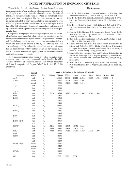
10-245This table lists the index of refraction of selected crystalline inor-ganic compounds. When, available, values are give as a function of wavelength in the range from the ultraviolet to the far infrared region. For each compound a value at 589 nm, the wavelength of the principal sodium line, is given. The data have been taken from the references indicated; in many cases, data from a reference have been refitted to generate the index of refraction at the wavelengths used in this table. All values refer to ambient temperature. Entries marked by * are based on extrapolation beyond the range of available exper-imental data.Compounds belonging to the cubic crystal system have only a sin-gle refractive index value, but other systems are anisotropic, so that the crystal is characterized by two or three unique indexes. Hexago-nal, rhombohedral, and tetragonal crystals have two unique indexes which are traditionally labeled n o and n e for “ordinary ray” and “extraordinary ray”. Orthorhombic, monoclinic, and triclinic crys-tals are characterized by three indexes which are here called n x , n y , and n z . The table indicates the crystal system for each entry in order to identify the material uniquely.The refractive index and other optical properties for metals, semi-conductors, and certain other compounds can be found in the tables “Optical Properties of Selected Elements” and “Optical Properties of Selected Inorganic and Organic Solids” in Section 12 of this Handbook .References1. Li, H. H., “Refractive Index of Alkali Halides and its Wavelength and Temperature Derivatives”, J. Phys. Chem. Ref. Data 5, 329, 1976.2. Li, H. H., “Refractive Index of Alkaline Earth Halides and its Wave-length and Temperature Derivatives”, J. Phys. Chem. Ref. Data 9, 161, 1980.3. Li, H. H., “Refractive Index of ZnS, ZnSe, and ZnTe and its Wave-length and Temperature Derivatives”, J. Phys. Chem. Ref. Data 13, 103, 1984.4. Shannon, R. D., Shannon, R. C., Medenbach, O., and Fischer, R. X., “Refractive Index and Dispersion of Fluorides and Oxides”, J. Phys. Chem. Ref. Data 31, 931, 2002.5. Gray, D. E., ed., American Institute of Physics Handbook , Sec. 6b, p. 6-12, McGraw-Hill, New York, 1972.6. Landolt-Börnstein Numerical Data and Functional Relationships in Science and Technology , III/11, Elastic, Piezoelectric, Pyroelectric, Piezooptic, Electrooptic Constants, and Nonlinear Dielectric Suscepti-bilities of Crystals, Springer-Verlag, Berlin, 1979.7. Landolt-Börnstein Numerical Data and Functional Relationships in Science and Technology , III/30A, High Frequency Properties of Dielec-tric Crystals. Piezooptic and Electrooptic Constants, Springer-Verlag, Berlin, 1996.8. Weber, M. J., CRC Handbook of Laser Science and Technology , V ol. IV . Optical Materials. Part 2: Properties, CRC Press, Boca Raton, FL, 1986.Crystal system Index of Refraction at the Indicated WavelengthCompound Ray 300 nm589 nm 750 nm 1 m 2 m5 m 10 m 20 m Ref.AgCl cub n 2.0668 2.0401 2.0224 2.0062 1.99751.98031.90695AlPO 4rhomb n o 1.5247 1.5203 1.5161 1.50346rhomb n e 1.5338 1.5290 1.52451.51166Al 2O 3hex n o 1.76734hex n e 1.75984As 2O 3a cub n 1.75374BaF 2cub n 1.5010 1.4744 1.4712 1.4686 1.4647 1.4511 1.40142BaO cub n 1.98414BaSO 4orth n x 1.63624orth n y 1.63744orth n z 1.64804BaTiO 3tetr n o 2.44054tetr n e 2.38314BaWO 4tetr n o 1.84264tetr n e 1.84054BeO hex n o 1.71844hex n e 1.73424BeSO 4⋅4H 2O tetr n o 1.47134tetr n e 1.43284CaCO 3b hex n o 1.7216 1.6584 1.6503 1.6436 1.62495hex n e 1.5145 1.4864 1.4828 1.4801 1.47535CaF 2cub n 1.4540 1.4338 1.4311 1.4289 1.42391.3990 1.2992CaO cub n 1.83964CaSO 4orth n x 1.56984orth n y 1.57554orth n z 1.61374CaSO 4⋅2H 2Omonocl n x 1.52074monocl n y 1.52274monocl n z 1.53044CaWO 4tetr n o 1.91954tetr n e 1.93554CdShexn o2.5072.390 2.3345INDEX OF REFRACTION OF INORGANIC CRYSTALShex ne2.525 2.409 2.3525CdSe hex no2.68* 2.5502 2.4682 2.4483 2.43317hex ne2.69* 2.5696 2.4873 2.4676 2.45147 CdTe cub n 2.6724 2.63027CeF3hex no1.61834hex ne1.61134CsBr cub n 1.8047 1.6974 1.6861 1.6784 1.6711 1.6678 1.6630 1.64391 CsCl cub n 1.712 1.640 1.631 1.626 1.620 1.616 1.606 1.5631CsClO4orth nx1.47524orth ny1.47884orth nz1.48044CsF cub n 1.506 1.477 1.474 1.472 1.469* 1.461* 1.436* 1.32*1 CsI cub n 1.9790 1.7873 1.7694 1.7576 1.7465 1.7428 1.7396 1.72801Cs2SO4orth nx1.55984orth ny1.56444orth nz1.56624CuBr cub n 2.1177 CuCl cub n 1.9727 1.9391 1.92457 CuSO4⋅5H2O tricl n x 1.51404tricl ny1.53674tricl nz1.54364Dy2O3cub n 1.97574FeF2tetr no1.5144tetr ne1.5244Gd2O3cub n 1.964HgS rhomb no2.9413 2.7770 2.7120 2.6305 2.60186rhomb ne3.3072 3.0896 3.0050 2.8776 2.85226 KBr cub n 1.6482 1.5598 1.5498 1.5444 1.5383 1.5345 1.5264 1.49241 KCl cub n 1.5455 1.4902 1.4840 1.4798 1.4753 1.4704 1.4564 1.39461KClO4orth nx1.47304orth ny1.47364orth nz1.47684KF cub n 1.380 1.362 1.360 1.358 1.355 1.344 1.304* 1.09*1KH2AsO4tetr no1.56747tetr ne1.51797KH2PO4tetr no1.5450 1.5093 1.5030 1.49575tetr ne1.4977 1.4682 1.4641 1.46065KI cub n 1.834* 1.665 1.650 1.640 1.631 1.627 1.620 1.5931KIO3tricl nx1.69597tricl ny1.83177tricl nz1.83437KIO4tetr no1.62054tetr ne1.64764KNbO3orth nx2.2480 2.3395 2.26127orth ny2.3464 2.2959 2.26227orth nx2.1803 2.1457 2.12887K2SO4orth nx1.49344orth ny1.49474orth nz1.49734LaF3hex no1.6054hex ne1.5994LiBr cub n 1.810 1.783 1.781 1.778 1.774* 1.756* 1.68* 1.33*1 LiCl cub n 1.677 1.662 1.660 1.658 1.654* 1.62* 1.53*1 LiClO4⋅3H2O hex n o 1.48324hex ne1.43844 LiF cub n 1.4087 1.3921 1.3895 1.3871 1.3786 1.3266 1.10051 LiI cub n 1.979 1.955 1.952 1.950 1.948* 1.940* 1.91* 1.77*1LiIO3hex no1.8875 1.8713 1.8589 1.84106hex ne1.7400 1.7268 1.7179 1.70626LiNbO3rhomb no2.3007 2.2632 2.23707rhomb ne2.2116 2.1804 2.15677LiTaO3rhomb no2.1864 2.1590 2.1391 2.10667rhomb ne2.1908 2.1634 2.1432 2.11157Li2SO4⋅H2O monocl n x 1.46154monocl ny1.47654monocl nz1.48634Lu2O3cub n 1.93494MgF2tetr no1.3930 1.3776 1.375 1.373 1.368 1.34 1.212tetr ne1.4055 1.3894 1.387 1.385 1.379 1.34 1.212MgO cub n 1.7355 1.7283 1.7228 1.7084 1.63615 MgSO4⋅7H2O orth n x 1.43264orth ny1.45554orth nz1.46074MnF2tetr no1.4724tetr ne1.5014NH4H2AsO4tetr no1.6401 1.5777 1.5704 1.55837tetr ne1.5754 1.5232 1.5179 1.51017NH4H2PO4tetr no1.5668 1.5247 1.5187 1.50847tetr ne1.5137 1.4797 1.4754 1.46947NaBr cub n 1.748 1.642 1.631 1.623 1.616 1.609 1.593* 1.520*1NaBrO3cub n 1.61684 NaCl cub n 1.6066 1.5441 1.5369 1.5320 1.5265 1.5188 1.4947 1.382*1NaClO3cub n 1.51517 NaF cub n 1.3424 1.3252 1.3231 1.3214 1.3179 1.3017 1.24001NaH2PO4⋅2H2O orth n x 1.44007orth ny1.46287orth nz1.48147NaI cub n 1.93* 1.774 1.758 1.74 1.73* 1.73* 1.71* 1.66*1NaNO2orth nx1.65477orth ny1.34557orth nz1.41257NaNO3rhomb no1.58405rhomb ne1.33405Na2HPO4⋅7H2O monocl n x 1.44114monocl ny1.44234monocl nz1.45254Na2SO4orth nx1.46694orth ny1.47304orth nz1.48094NdF3hex no1.61914hex ne1.61324Nd2O3cub n 1.924NiF2tetr no1.5264tetr ne1.5614NiSO4⋅6H2O tetr n o 1.51074tetr ne1.48704PbF2cub n 1.94* 1.767 1.754 1.745 1.73 1.70 1.66 1.325PbSO4orth nx1.87804orth ny1.88344orth nz1.89454PrF3hex no1.62074hex ne1.61464RbBr cub n 1.639 1.553 1.544 1.538 1.532 1.530 1.525 1.505*1 RbCl cub n 1.549 1.493 1.487 1.483 1.479 1.475 1.465 1.424*1RbClO4orth nx1.46914orth ny1.47014orth nz1.47324RbF cub n 1.428* 1.397 1.394 1.391 1.388 1.379 1.346 1.19*1RbH2AsO4tetr no1.6183 1.5603 1.5538 1.54327tetr ne1.5718 1.5232 1.5184 1.51217RbH2PO4tetr no1.5434 1.5078 1.5021 1.49417tetr ne1.5106 1.4791 1.4754 1.47047RbI cub n 1.808 1.647 1.633 1.623 1.615 1.612 1.608 1.5951Rb2SO4orth nx1.51314orth ny1.51334orth nz1.51444Sb2O3c cub n 2.80174Sc2O3cub n 1.99434SiO2d hex n o 1.5733 1.5442 1.5394 1.5350 1.52095hex ne1.5882 1.5534 1.5484 1.5438 1.52915SnO2tetr no1.9934tetr ne2.0884SrF2cub n 1.459 1.4380 1.435 1.433 1.429 1.412 1.352 SrO cub n 1.87104SrSO4orth nx1.62144orth ny1.62314orth nz1.63034SrTiO3cub n 2.4082 2.3525 2.3160 2.2676 2.12055SrWO4tetr no1.86184tetr ne1.87194TbF3hex no1.60344hex ne1.56034TeO2tetr no2.2738 2.20807tetr ne2.4295 2.35207ThO2cub n 2.11134TiO2e tetr n o 2.612 2.533 2.485 2.399 2.2205tetr ne2.910 2.805 2.7485tetr no2.5624tetr ne2.4894 TlBr cub n 2.418 2.350 2.289 2.103 1.984 2.339 2.3225 TlCl cub n 2.247 2.198 2.145 1.986 1.891 2.1935TlClO4orth nx1.64274orth ny1.64464orth nz1.65424Tl2SO4orth nx1.86044orth ny1.86764orth nz1.88574Y2O3cub n 1.9304Yb2O3cub n 1.94684ZnF2tetr no1.4954tetr ne1.5254ZnO hex no2.0036 1.9662 1.9435 1.91977hex ne2.0199 1.9821 1.9589 1.93307 ZnS f cub n 2.3691 2.3232 2.2932 2.26337ZnS g hex no2.372 2.331 2.303 2.26 2.25 2.203,5hex ne2.368 2.327 2.3015 ZnSe cub n 2.6222 2.5384 2.4888 2.4462 2.4296 2.40653 ZnTe cub n3.060 2.880 2.789 2.719 2.698 2.6843ZrSiO4h tetr n o 1.92554tetr ne1.98434 *Provisional value based on extrapolation beyond the range of experimental data.a Arsenoliteb Calcitec Senarmontitedα-Quartze Rutilef Sphaleriteg Wurtziteh Zircon。
Electrical and Optical Properties of InGaNAlGaN Double Heterostructure Blue Light-Emitting
PACS: 78. 60. Fi, 73. 40. Kp
Recently, the wide band gap semiconductors GaN, InN, AlN and their alloys have attracted considerable interest because of their great potential applications in electronics and optoelectronics.1 2 They may be used in the fabrication of light-emitting diodes (LEDs) and lasers operating in the visible and ultraviolet (UV).3 4 With the development of the materials and devices, an energy span ranging from the blue to near-UV wavelengths, which was inaccessible to semiconductor technology in the past, has been opened. Recently, group III nitride-based electronic devices are being developed for various applications, most notably for blue laser diodes (LDs) and high-temperature electronics. In addition, the blue LEDs are the most mature amongst the nitride-based optoelectronic components, having been successfully commercialized since 1994. Several papers on high-brightness InGaN/AlGaN blue LEDs from the Nichia Chemical Industries Ltd have shown some behaviours of the emission spectra with various current injections.5;7 Electrical and optical characterization of the devices can provide important information about the current transport through wide band gap p{n heterojunctions, layer materials and metal{ semiconductor contacts.8 9 So far, however, these aspects of nitride-based LEDs have received relatively little attention. In this study, the electrical and optical properties of the InGaN/AlGaN double heterostructure blue LEDs made by Nichia Ltd were investigated at 77 and 300 K. It was found that the main transport mechanism was associated with carrier tunnelling, rather than thermal di usion. Electroluminescence (EL) experiments indicated there was an emission band around 2.80 eV and a relatively weaker shortwavelength peak at 3.2 eV. Furthermore, the degradation in the I ; V characteristics and the low resistance ohmic short were observed. The Nichia blue LEDs used in this study were of double heterostructures (DHs) with an n-type In0 06 Ga0 94 N active layer co-doped with the donor Si and the acceptor Zn.10 11 The epitaxial layers were grown by the two- ow metal organic chemical vapour deposition (MOCVD) method on (0001) oriented sapphire substrates. The 30 nm thick Si-doped GaN bu er layer was rst grown at 510 C, and the 4 m thick Si-doped GaN layer was grown at 1020 C. The Si-doped Al0 15 Ga0 85 N layer for the carrier con nement was 0.15 m in thickness. The 50 nm thick In0 06 Ga0 94 N active layer co-doped with the donor Si and the acceptor Zn was grown at 780 C. The thin active layer and the Al0 15 Ga0 85 N con nement layers ensure a region of uniform excitation and the EL in the active region results from e cient recombination of carriers via Zn-related deep levels. Therefore, the spontaneous emission spectra will be a replica of the minority carrier distribution. Prior to measurements, the diodes were deencapsulated to avoid the risk of epoxy-induced stress at the cryogenic temperatures. The direct current I ; V measurements were performed at 77 K and room temperature (300 K). For the measurements at 77 K, the diode was xed on a cold nger in a vacuum chamber that was kept at the temperature of liquid nitrogen. In order to understand the possible relationship between the current components and light emission, optical experiments were performed using a monochromator, a chopper or signal generator, and a UV photomultiplier equipped with an EG&G 5210 lock-in ampli er. The forward bias I ; V behaviours for a blue LED
Optical Properties of Tissue组织光学特性参数

Mie scattering
生命科学与技术学院•生物医学光子学教育部重点实验室
Rayleigh scattering
Size<< isotropic scattering Stronger scattering at short wavelengths s~1/4
生命科学与技术学院•生物医学光子学教育部重点实验室
17
geometrical effective cross-section cross-section 生命科学与技术学院•生物医学光子学教育部重点实验室
Scattering coefficient(散射系数)
[cm-1] [cm-3] [cm2]
Scattering length
生命科学与技术学院•生物医学光子学教育部重点实验室
生命科学与技术学院•生物医学光子学教育部重点实验室
24
Origins of scattering
The scattering properties of tissue are dominated by the lipid-water interfaces presented by membranes in cells (especially membranes in mitochondria), by nuclei, and by protein fibers such as collagen or actin-myosin.
cos() cos()
生命科学与技术学院•生物医学光子学教育部重点实验室
20
Equivalent Random Walk
26
生命科学与技术学院•生物医学光子学教育部重点实验室
21
【精品】材料科学与工程(Materials Science and Engineering)专业英语讲义word版

材料科学与工程专业英语Materials Science and EngineeringUnit1Materials Science and EngineeringMaterials are properly more deep-seated in our culture than most of us realize. 材料可能比我们大部分人所意识到的更加深入地存在于我们的文化当中。
Transportation, housing, clothing, communication, recreation and food production-virtually every segment of our lives is influenced to one degree or another by materials.运输、住房、衣饰、通讯、娱乐,还有食品生产——实际上我们日常生活的每个部分都或多或少地受到材料的影响。
Historically, the development and advancement of societies have been int imately tied to the members’ abilities to produce and manipulate materials to fill their needs. 从历史上看,社会的发展和进步已经与社会成员生产和利用材料来满足自身需求的能力紧密地联系在一起。
In fact, early civilizations have been designated by the level of their materials development.事实上,早期文明是以当时材料的发展水平来命名的。
(也就是石器时代,青铜器时代)The earliest humans has access to only a very limited number of materials, those that occur naturally stone, wood, clay, skins, and so on. 最早的人类只能利用非常有限数量的材料,象那些自然界的石头,木头,黏土和毛皮等等。
Advanced Optical Properties of Materials
Advanced Optical Properties of
Materials
随着科学技术的不断发展,材料科学也在不断的进步中,特别是光学材料。
随着人们对光的认识日益深入,对光学材料的要求也越来越高。
光学材料的最主要特性是它的光学性能,其中不乏一些现代先进的光学特性。
一、色变效应
色变效应是指材料在不同光照条件下颜色的变化。
银石墨烯是一种新型的色变材料,在光的作用下,在低波长光照下高透过率,红外光照下低透过率。
这种颜色变化可用来制备智能光学器件。
二、荧光效应
荧光效应是指材料在受到激发后在某些波长下发出荧光光谱。
荧光材料广泛应用于生物医药检测、紫外线检测等领域。
例如,氧化钆蛋白是一种荧光材料,具有很快的响应速度和高的灵敏度。
它可以广泛应用于微生物检测、环境污染检测等领域。
三、电致变色效应
电致变色效应是指材料在电场作用下,颜色的变化。
这种效应被广泛应用于信息显示、太阳能电池等领域。
例如,铁氰化铁是一种电致变色材料,可以广泛应用于电致变色太阳能电池的制备。
四、光子晶体效应
光子晶体效应是指材料在受到特定波长的光照射时会发生厚度对波长的选择性反射。
这种效应可被应用于光通信、光电子器件等领域。
例如,聚苯乙烯是一种光子晶体材料,可以用来制备窄波长滤光器、超光速光学器件等。
总之,现代先进的光学特性是材料科学持续发展的产物,其中每一个特性都对应着特定的应用领域,具有巨大的应用价值。
未来,将有越来越多的先进光学特性被发现和应用。
Exploring the Optical Properties of Materials
Exploring the Optical Properties ofMaterialsMaterials can have a range of optical properties, depending on their composition, structure, and interactions with light. Understanding these properties can help us develop new materials for a variety of applications, from optical data storage to solar cells.One of the most fundamental optical properties of materials is their refractive index, which describes how much the speed of light is reduced when it travels through the material. This property is determined by the electronic and atomic structure of the material, as well as the density and arrangement of its atoms.Another important optical property is absorption, which occurs when a material absorbs certain wavelengths of light and re-emits the energy as heat or fluorescence. Different materials absorb light differently depending on their electronic structure and the energy of the incoming photons. This property is useful in applications like photovoltaics, where materials that absorb certain wavelengths of light well can be used to convert that light into energy.Reflection is also an important optical property. When light hits a surface, some of it is reflected back and some of it is transmitted through. The amount that is reflected depends on the angle of incidence, the polarization of the light, and the roughness of the surface. This property is important in applications like mirrors and optical coatings, where materials that reflect light well are desired.The interaction of materials with light can also cause them to emit their own light in a process called luminescence. This property can be used in applications like lighting and imaging, where materials that emit light in certain wavelengths are desired. Luminescence can also be used to study the electronic structure of materials, as different materials emit light in different ways.Understanding the optical properties of materials is also important for developing new technologies like optical computing and communication. Light can be used to carry information through optical fibers, which have low absorption and high reflection properties. Optical materials can also be used to manipulate or modulate light signals, allowing for the development of new optical devices.Overall, the exploration of optical properties in materials is a fascinating field that offers endless possibilities for new technologies and applications. By understanding how materials interact with light, we can develop new materials that can convert, manipulate, and transmit light in exciting and useful ways.。
光有源器件和无源器件的英文
IntroductionElectronic devices, the backbone of modern technology, rely on a diverse array of components that function in concert to process, transmit, and store information. These components can be broadly classified into two distinct categories: active and passive electronic devices. Each category exhibits unique characteristics, functionalities, and roles within electronic circuits, contributing to the overall performance and efficiency of various systems. This comprehensive analysis delves into the fundamental principles, operational mechanisms, applications, and comparative perspectives of active and passive electronic components, providing a thorough understanding of their significance in the realm of electronics.Active Electronic ComponentsActive electronic components are the driving force behind any circuit, as they possess the ability to control, amplify, or generate electrical signals without relying solely on the input signal. They require an external source of energy, typically in the form of a DC power supply, to perform their designated functions. The primary distinguishing feature of active components is their capacity to introduce gain, which refers to the amplification of an input signal's voltage, current, or power. The most common examples of active components include transistors (bipolar junction transistors, field-effect transistors), integrated circuits (ICs), diodes, and vacuum tubes.1. **Operational Principles**: Active components manipulate electrical signals through the control of electron flow. For instance, transistors employ the principles of charge carrier injection and modulation to amplify or switch signals. Diodes, on the other hand, utilize the property of asymmetric conductivity to allow current flow predominantly in one direction. Integrated circuits incorporate multiple active and passive components on a single chip, enabling complex signal processing and control functions.2. **Applications**: Active components find widespread use in virtually allswitches, oscillators, and logic gates in digital circuits. ICs are integral to microprocessors, memory chips, and analog-to-digital converters, enabling computing, communication, and control systems. Diodes are employed in rectifiers, voltage regulators, and signal demodulation circuits. Vacuum tubes, although less prevalent today, still have niche applications in high-power amplifiers, radio transmitters, and specialized audio equipment.3. **Advantages**: Active components offer several advantages, such as signal amplification, voltage and current regulation, non-linear signal processing, and the ability to create complex logical operations. They enable the creation of highly efficient and miniaturized electronic systems, thanks to advancements in IC technology.Passive Electronic ComponentsPassive electronic components, in contrast, do not require a source of external energy for their operation. They simply respond to the applied electrical signals, storing, dissipating, or redirecting energy without introducing gain. The primary passive components include resistors, capacitors, inductors, transformers, and various types of connectors and cables.1. **Operational Principles**: Passive components rely on fundamental electrical properties to perform their functions. Resistors impede current flow based on Ohm's Law, converting electrical energy into heat. Capacitors store electrical energy in an electric field, releasing it when required, while inductors store energy in a magnetic field and oppose changes in current. Transformers utilize electromagnetic induction to transfer energy between circuits with different voltage levels, while connectors and cables facilitate the transmission of signals without significant attenuation or distortion.2. **Applications**: Passive components are ubiquitous in electronic circuits, serving essential roles in filtering, impedance matching, signal coupling, power distribution, and timing. Resistors are used for voltage division, current limiting, and pull-up/pull-down configurations. Capacitorssmoothing power supplies, and resonant circuits. Transformers are critical in power supply isolation, stepping up or down voltages, and signal coupling across different impedances. Connectors and cables ensure reliable signal transmission in various systems, from consumer electronics to large-scale industrial installations.3. **Advantages**: Passive components offer simplicity, reliability, and cost-effectiveness. They do not generate noise or consume power, making them ideal for signal conditioning and energy management tasks. Moreover, their non-reactive nature simplifies circuit analysis and design.Comparative PerspectivesWhile both active and passive components are indispensable in electronic circuits, their roles and characteristics differ significantly:1. **Energy Consumption**: Active components consume power to perform their functions, whereas passive components do not. This distinction influences power budgeting, thermal management, and battery life considerations in electronic designs.2. **Signal Amplification**: Active components can amplify signals, whereas passive components cannot. This capability is crucial for signal processing, long-distance transmission, and overcoming inherent signal losses in electronic systems.3. **Complexity**: Active components, particularly ICs, can integrate vast numbers of active and passive elements on a single chip, enabling highly complex and sophisticated circuits. Passive components, while essential, generally contribute to the circuit's overall simplicity and ease of maintenance.4. **Noise Generation**: Active components, due to their internal processes, can introduce noise into a circuit, which may need to be mitigated through careful design and filtering. Passive components, being inherently non-amplifying, tend to produce less noise.Conclusionblocks of modern electronics, each playing a unique and indispensable role in shaping the functionality and performance of electronic systems. While active components, with their signal amplification and energy-consuming nature, drive the core processing and control functions, passive components provide essential support through energy storage, signal conditioning, and power distribution. Understanding the operational principles, applications, and comparative perspectives of these components is vital for engineers and designers seeking to create efficient, reliable, and high-performance electronic devices and systems.。
光学专业英语50句翻译
光学专业英语50句翻译1.The group's activities in this area have concentrated on the mechanicaleffects of angular momentum on a dielectric and on the quantum properties of orbital angular momentum.在这个研究领域,这个研究组主要集中在电介质中的角动量的机械效应和轨道角动量的量子属性。
2. Experimental realization of entanglement have been restricted totwo-state quantum systems. In this experiment entanglement exploiting the orbital angular momentum of photons, which are states of the electromagnetic field with phase singularities (doughnut modes).纠缠的实验认识还只停留在二维量子系统。
在这实验中,利用了光子的轨道角动量的纠缠是具有相位奇点(暗中空模式)的电磁场的状态。
3. Laguerre Gaussian modes with an index l carry an orbital angular momentum of per photon for linearly polarized light that is distinct from the angular momentum of the photons associated with their polarization对线偏振光来说,具有因子l的LG模式的每个光子能携带的轨道角动量,这是与偏振态相关的光子的角动量是截然不同的。
法布里珀罗基模共振英文

法布里珀罗基模共振英文The Fabryperot ResonanceOptics, the study of light and its properties, has been a subject of fascination for scientists and researchers for centuries. One of the fundamental phenomena in optics is the Fabry-Perot resonance, named after the French physicists Charles Fabry and Alfred Perot, who first described it in the late 19th century. This resonance effect has numerous applications in various fields, ranging from telecommunications to quantum physics, and its understanding is crucial in the development of advanced optical technologies.The Fabry-Perot resonance occurs when light is reflected multiple times between two parallel, partially reflective surfaces, known as mirrors. This creates a standing wave pattern within the cavity formed by the mirrors, where the light waves interfere constructively and destructively to produce a series of sharp peaks and valleys in the transmitted and reflected light intensity. The specific wavelengths at which the constructive interference occurs are known as the resonant wavelengths of the Fabry-Perot cavity.The resonant wavelengths of a Fabry-Perot cavity are determined bythe distance between the mirrors, the refractive index of the material within the cavity, and the wavelength of the incident light. When the optical path length, which is the product of the refractive index and the physical distance between the mirrors, is an integer multiple of the wavelength of the incident light, the light waves interfere constructively, resulting in a high-intensity transmission through the cavity. Conversely, when the optical path length is not an integer multiple of the wavelength, the light waves interfere destructively, leading to a low-intensity transmission.The sharpness of the resonant peaks in a Fabry-Perot cavity is determined by the reflectivity of the mirrors. Highly reflective mirrors result in a higher finesse, which is a measure of the ratio of the spacing between the resonant peaks to their width. This high finesse allows for the creation of narrow-linewidth, high-resolution optical filters and laser cavities, which are essential components in various optical systems.One of the key applications of the Fabry-Perot resonance is in the field of optical telecommunications. Fiber-optic communication systems often utilize Fabry-Perot filters to select specific wavelength channels for data transmission, enabling the efficient use of the available bandwidth in fiber-optic networks. These filters can be tuned by adjusting the mirror separation or the refractive index of the cavity, allowing for dynamic wavelength selection andreconfiguration of the communication system.Another important application of the Fabry-Perot resonance is in the field of laser technology. Fabry-Perot cavities are commonly used as the optical resonator in various types of lasers, providing the necessary feedback to sustain the lasing process. The high finesse of the Fabry-Perot cavity allows for the generation of highly monochromatic and coherent light, which is crucial for applications such as spectroscopy, interferometry, and precision metrology.In the realm of quantum physics, the Fabry-Perot resonance plays a crucial role in the study of cavity quantum electrodynamics (cQED). In cQED, atoms or other quantum systems are placed inside a Fabry-Perot cavity, where the strong interaction between the atoms and the confined electromagnetic field can lead to the observation of fascinating quantum phenomena, such as the Purcell effect, vacuum Rabi oscillations, and the generation of nonclassical states of light.Furthermore, the Fabry-Perot resonance has found applications in the field of optical sensing, where it is used to detect small changes in physical parameters, such as displacement, pressure, or temperature. The high sensitivity and stability of Fabry-Perot interferometers make them valuable tools in various sensing and measurement applications, ranging from seismic monitoring to the detection of gravitational waves.The Fabry-Perot resonance is a fundamental concept in optics that has enabled the development of numerous advanced optical technologies. Its versatility and importance in various fields of science and engineering have made it a subject of continuous research and innovation. As the field of optics continues to advance, the Fabry-Perot resonance will undoubtedly play an increasingly crucial role in shaping the future of optical systems and applications.。
光纤光学英语大全
光学专业词汇大全Iris – aperture stop虹膜孔俓光珊retina视网膜Color Blind 色盲weak color 色弱Myopia –near-sighted 近视Sensitivity to Light感光灵敏度boost推进lag behind落后于Hyperopic – far-sighted 远视Dynamic Range 动态范围critical fusion frequency 临界融合频率CFF临界闪变频率visual sensation 视觉Chromaticity Diagram色度图Color Temperature色温HSV Model色彩模型(hue色度saturation饱和度value纯度CIE Model 相干红外能量模式Complementary Colors补色Bar Pattern条状图形Heat body 热稠化approximate近似violet紫罗兰Body Curve人体曲线Color Gamut色阶adjacent邻近的normal illumination法线照明Primary colors红黄蓝三原色Color saturation色饱和度Color Triangle颜色三角Color Notation颜色数标法Color Difference色差TV Signal Processing电视信号处理Gamma Correction图像灰度校正Conversion Tables换算表out of balance失衡wobble摇晃back and forth前后clear (white) panel 白光板vibrant震动fuzzy失真quantum leap量子越迁SVGA (800x600)derive from起源自culprit犯人render呈递inhibit抑制,约束stride大幅前进blemish污点obstruction障碍物scratch刮伤substance物质实质主旨residue杂质criteria标准parameter参数adjacent邻近的接近的asynchrony异步cluster串群mutually互助得algorithm运算法则Chromatic Aberrations色差Fovea小凹Visual Acuity视觉灵敏度Contrast Sensitivity对比灵敏度Temporal (time) Response反应时间rendition表演,翻译animation活泼又生气ghost重影Parallax视差deficient缺乏的不足的Display panel显示板NG.( Narrow Gauge)窄轨距dichroic mirror二色性的双色性的Brewster Angle布鲁斯特角Polarized Light极化光Internal reflection 内反射Birefringence 双折射Extinction Ratio 消光系数Misalignment 未对准Quarter Waveplates四分之一波片blemish污点瑕疵Geometric几何学的ripple波纹capacitor电容器parallel平行的他tantalum钽(金属元素) exsiccate使干燥exsiccate油管,软膏furnace炉子镕炉electrolytic电解的,由电解产生的module 模数analog类似物out of the way不恰当pincushion针垫拉lateral侧面得rectangle长方形fixture固定设备control kit工具箱DVI connector DVI数局线Vertical垂直的horizontal 水平的interlace隔行扫描mullion竖框直楞sawtooth锯齿toggle套索钉keypad数字按键键盘tangential切线diagnostic tool诊断工具sagittal direction径向的cursor position光标位置3Yw'/#p3`ray aberration光线相差weighting factor权种因子variables变量for now暂时,目前.眼下check box复选框Airy disk艾里斑exit pupil出[射光]瞳optical path difference光称差with respect to关于diffraction limited 衍射极限wavefront aberration波阵面相差spherical aberration球面象差paraxial focus傍轴焦点chromatic aberration象差local coordinate system局部坐标系统coordinate system坐标系orthogonal直角得,正交的conic sections圆锥截面account for解决,得分parabolic reflector拋物面反射镜radius ofcurvature曲率半径spherical mirror球面镜geometrical aberration几何相差incident radiation入射辐射global coordinate总体坐标in terms of根据按照reflected beam反射束FYI=for your information供参考Constructive interference相长干涉phase difference相差achromatic singlet消色差透镜Interferometer 干涉仪boundary constraint边界约束,池壁效应radii半径Zoom lenses变焦透镜Beam splitters分束器discrete不连续的,分离的objective/eye lens物镜/目镜mainframe主机rudimentary根本的,未发展的photographic照相得摄影得taxing繁重的,费力得algebra代数学trigonometry三角学geometry几何学calculus微积分学philosophy哲学lagrange invariant拉格朗日不变量spherical球的field information场信息Standard Lens标准透镜Refracting Surface折射面astigmatism散光HDTV高清晰度电视DLV ( Digital Light Valve)数码光路真空管,简称数字光阀diffraction grating衍射光珊field angle张角paraxial ray trace equations近轴光线轨迹方称back focal length后焦距principal plane主平面vertex顶点,最高点astigmatism散光,因偏差而造成的曲解或错判medial中间的,平均的variance不一致conic圆锥的,二次曲线field of view视野collimator瞄准仪convolution回旋.盘旋,卷积fuzzy失真,模糊aberrated异常的asymmetry不对称得indicative可表示得parabolic拋物线得suffice足够,使满足specification规格,说明书straightforward易懂的,直接了当的,solidify凝固,巩固. Constraints 约束,限制metrology度量衡field coverage视场,视野dictate口述, 口授, 使听写, 指令, 指示, 命令, 规定irradiance发光, 光辉,辐照度aerial空气得,空中得halide卤化物的monochromatic单色的,单频的polychromatic多色的aspherical非球面的spherical球面的alignment列队,结盟power(透镜)放大率equiconvergence 同等收敛EFL(effective focal length)有效焦距workhorse广为应用的设备biconvex两面凸的global optimization整体最优化concave凹得,凹面得cylindrical圆柱得solid model实体模型Modulation Transfer Function调制传递函数in the heat of在最激烈的时候protocol协议,规定triplet三重态sanity心智健全zinc锌,涂锌的selenide 硒化物,硒醚miscellaneous各色各样混在一起, 混杂的, 多才多艺的versus与...相对polynomial多项式的coefficient系数explicit function显函数" wYgi%distinct清楚的,截然不同的emanate散发, 发出, 发源rudimentary根本的,未发展的intersection角差点PRTE=paraxial ray trace equation旁轴光线轨迹方程achromats 消色差透镜cardinal points基本方位separations分色片dashed虚线blow up放大overlay覆盖,覆盖图multiplayer 多层的humidity 湿度float glass浮法玻璃square one 出发点,端点square up to 准备开打,坚决地面对reflecting telescope 反射式望远镜diagnostic tools诊断工具Layout plots规划图Modulation transfer function调制转换功能FFT快速傅里叶变换Point spread function点传播功能wavelength波长angle角度absorption吸收system aperture 系统孔径lens units透镜单位wavelength range波长范围singlet lens单业透镜spectrum光谱diffraction grating衍射光栅asphere半球的LDE=Lens data editor Surface radius of curvature表面曲率半径surfacethickness表面厚度material type材料种类semi-diameter半径focal length焦距aperture type孔径类型aperture value孔径值field of view视场microns微米F, d, and C= blue hydrogen, yellow helium, red hydrogen lines, primary wavelength主波长sequential mode连续模式object surface物表面The front surface of the lens透镜的前表面stop光阑The back surface of the lens透镜的后表面The image surface 像表面symmetric相对称的biconvex两面凸的The curvature is positive if the center of curvature of the surface is to the right of the vertex. It is negative if the center of curvature is to the left of the vertex.如果曲率中心在最高点的右边,曲率值为正,如果曲率中心在最高点的左边,则曲率为负image plane像平面Ray Aberration光线相差tangential direction切线方向sagittal direction径向paraxial focus旁轴的Marginal 边缘的spherical aberration球面像差Optimization Setup最优化调整variable变量mathematical sense 数学角度MFE= Merit Function Editor, Adding constraints增加约束focal length焦矩长度operand操作数the effective focal length有效焦矩primary wavelength主波长initiate开始spot diagram位图表Airy disk 艾里斑axial chromatic aberration轴向色差with respect to关于至于exit pupil出射光瞳OPD=optical path difference光学路径差diffraction limited衍射极限chromatic aberration色差chromatic focal shift色焦距变换paraxial focus傍轴焦点axial spherical aberration轴向球差(longitudinal spherical aberration 纵向球差:沿光轴方向度量的球差)lateral spherical aberration垂轴球差(在过近轴光线像点A‵的垂轴平面内度量的球差)coma、comatic aberration彗差meridional coma子午彗差sagittal coma弧矢彗差astigmatism像散local coordinate system本地坐标系统meridional curvature of field子午场曲sagittal curvature of field弧矢场曲decentered lens偏轴透镜orthogonal直角的垂直的conic section圆锥截面account for说明,占有,得分stigmatic optical system无散光的光学系统Newtonian telescope牛顿望远镜parabolic reflector抛物面镜foci焦距chromatic aberration,色差superpose重迭parabola抛物线spherical mirror球面镜RMS=Root Mean Square均方根wavefront波阵面spot size光点直径Gaussian quadrature高斯积分rectangular array矩阵列grid size磨粒度PSF=Point Spread Function点扩散函数FFT=Fast Fourier Transform Algorithm快速傅里叶变换Cross Section横截面Obscurations昏暗local coordinates局部坐标系统vignette把…印为虚光照Arrow key键盘上的箭头键refractive折射reflective反射in phase同相的协调的Ray tracing光线追迹diffraction principles衍射原理order effect式样提出的顺序效果energy distribution能量分配Constructive interference相长干涉dispersive色散的Binary optics二元光学phase advance相位提前achromatic single消色差单透镜diffractive parameter衍射参数Zoom lenses变焦透镜Athermalized lenses绝热透镜Interferometers干涉计Beam splitter分束器Switchable component systems可开关组件系统common application通用symmetry对称boundary constraint边界约束multi-configuration (MC) MC Editor (MCE) perturbation动乱,动摇index accuracy折射率准确性indexhomogeneity折射率同种性index distribution折射率分配abbe number离差数Residual剩余的Establishing tolerances建立容差figure of merit质量因子tolerance criteria公差标准Modulation Transfer Function (MTF)调制传递函数boresight视轴,瞄准线Monte Carlo蒙特卡洛Tolerance operands误差操作数conic constant ]MC1"{_qT圆锥常数astigmatic aberration像散误差Mechanical tilt机械倾斜,机械倾角Tolerance Data Editor (TDE)公差资料编辑器compensator补偿棱镜estimated system performance预估了的系统性能iteratively反复的,重迭的statistical dependence统计相关性sequential ray trace model连续光线追迹模型imbed埋葬,埋入multiple多样的,多重的,若干的Non-Sequential Components不连续的组件Corner cube角隅棱镜,三面直角透镜Sensitivity Analysis灵敏度分析Faceted reflector有小面的反射镜emit发射,发出nest嵌套overlap交迭outer lens外透镜brute force强力seidel像差系数aspect ratio长宽比MRA边缘光线角MRH边缘光线高度asynchronous不同时的,异步Apodization factor变迹因子hexapolar六角形dithered 高频脉冲衍射调制传递函数(DMTF),衍射实部传递函数(DRTF),衍射虚部传递函数(DITF),衍射相位传递函数(DPTF),方波传递函数(DSWM)logarithmic对数的parity奇偶% Uc,I e longitudinal aberrations 纵向像差赛得系数: 球差(SPHA,SI),彗差(COMA,S2),像散(ASTI,S3),场曲(FCUR,S4),畸变(DIST,S5),轴向色差(CLA,CL)和横向色差(CTR,CT).横向像差系数:横向球差(TSPH),横向弧矢彗差(TSCO),横向子午彗差(TTCO),横向弧矢场曲(TSFC),横向子午场曲(TTFC),横向畸变(TDIS)横向轴上色差(TLAC)。
Optical properties of the metals Al, Co, Cu, Au, Fe, Pb, Ni, Pd,
Fig. 3.
Gold: -e,(w) and e2(W) vs frequency.
The solid line is the
Drude model. The data from Ref. 9 are: Bennett and Bennett, *
for both -el and e2; Schulz, 0 for both; Motulevich and Shubin, for both; Padalka and Shklyarevskii, 0 for both; Bolotin et al., x for both; Brandli and Sievers, + for both; Weaver et al., A for both.
1
(6)
1 April 1983 / Vol. 22, No. 7 / APPLIED OPTICS
1099
106
105
105
14) N In Z
14)
In Z kV
102
102
101
101
100 102 103 105 FREQUENC.W (CM'1)
100 00 102 103 FREQUENCY, (CM'l W
O0 14
AX
14)
In rIn a: Z 10
ox °x
2
it AOA XA
14)
10I
4,
X
10'
SILVER
IRON
x x
100 o 10 0 102 11 10
5
X X
10I
10
100
t02
3
103
爱因斯坦的简介英文
爱因斯坦的简介英文阿尔伯特·爱因斯坦,犹太裔物理学家,被公认为是继伽利略、牛顿以来最伟大的物理学家,下面是店铺为你整理的爱因斯坦的简介英文,希望对你有用!阿尔伯特·爱因斯坦简介Albert Einstein (Albert.Einstein, March 14, 1879 - April 18, 1955), Jewish physicist.Einstein was born in 1891 in Ulm, Germany, a Jewish family (parents are Jews), 1900 graduated from the Zurich Federal Institute of Technology, into the Swiss nationality. In 1905, by the University of Zurich Ph.D., Einstein proposed photon hypothesis, successfully explained the photoelectric effect, so won the 1921 Nobel Prize in Physics, the creation of special relativity. In 1915 founded the general theory of relativity.Einstein laid the theoretical foundation for nuclear energy development, creating a new era of modern science and technology, is recognized as Galileo, Newton since the greatest physicist. December 26, 1999, Einstein was the United States, "Time magazine" named "century great man".阿尔伯特·爱因斯坦主要成就relativityThe creation of special relativity:As early as the age of 16, Einstein learned from the book that the light is moving rapidly with the speed of electromagnetic waves, linked to this, he would like to explore the so-called ether with the light of the problem. The name of the ether comes from Greece, to represent the basic elements that make up the objects of heaven. The 17th century Descartes and the subsequent Christian Huygens pioneered and developed the theory of ether,that the ether is the medium of light propagation, it is full of space, including vacuum, and can penetrate into the material. Unlike ether, Newton made the light particles say. Newton believes that the luminous body is emitted by a linear motion of particles of particles flow, particle flow impact of the retina caused vision. 18th century Newton's particles said the upper hand, the 19th century, it is volatile that accounted for an absolute advantage. The theory of ether is also greatly developed: the wave of the need for media transmission, light in the vacuum is the transmission of the media, also known as light ether. At the same time, the electromagnetism has been flourishing, through the Maxwell, Hertz and others efforts to form a mature electromagnetic phenomenon dynamics theory - electrodynamics, and from the theory and practice to prove that the light is a certain frequency range of electromagnetic waves , Thus unifying the wave theory of light and electromagnetic theory. The ether is not only the carrier of the light, but also the carrier of the electromagnetic field. Until the end of the nineteenth century, people tried to find the ether, but never found in the experiment ether, on the contrary, Michelson Morey experiment found that the ether is unlikely to exist.The development of electromagnetism was originally incorporated into the framework of Newtonian mechanics, but in interpreting the electromagnetic process of moving objects it was found that the relativity principle followed by Newtonian mechanics was inconsistent. According to Maxwell's theory, the velocity of electromagnetic waves in vacuum, that is, the speed of light is constant; however, according to Newton's method of velocity addition, the speed of light of different inertial lines is different. For example, two cars, one approaching to you, oneaway. You see the lights of the front car close to you, after a car light away. According to Galileo theory, the car coming to you will emit light with a speed greater than c (vacuum light velocity 3.0x10 ^ 8m / s), that is, the speed of the light in front of the vehicle = speed of light + speed; and the speed of light from the vehicle is less than The speed of the rear car light = speed of light - speed. But according to the speed of the two light the same, because in Maxwell's theory, the speed of the car does not affect the spread of light, that white regardless of how the car, the speed of light is equal to c. Maxwell and Galileo on the speed of the argument is clearly contrary!Einstein seems to be the one who will build a new physics building. Einstein carefully studied Maxwell's theory of electromagnetism, especially through the development and elaboration of electrodynamics by Hertz and Lorentz. Einstein firmly believes that the electromagnetic theory is completely correct, but there is a problem that makes him uneasy, this is the absolute reference to the presence of the ether. He read many of the works found that everyone tried to prove that the existence of the ether test is a failure. After studying Einstein found that, in addition to the absolute reference system and the electromagnetic field of the load, the ether in the Lorentz theory has no practical significance.Einstein loves to read philosophical works and absorb thought and nutrition from philosophy, and he believes in the unity and logical coherence of the world. The suspicion of the general validity of the causal law at David Hume in the Olympia Academy of Sciences has had an impact on Einstein. The principle of relativity has been widely proved in mechanics, but can not be established in electrodynamics, for the two theoretical systemsof physics in the logical inconsistency, Einstein raised doubts. In his view, the principle of relativity should be generally established, so the electromagnetic theory for each inertial system should have the same form, but here there is the problem of speed of light. Whether the speed of light is constant or variable, becomes the primary problem of whether the principle of relativity is universally established. At that time the physicists generally believed in the ether, that is, believe that there is an absolute reference system, which is affected by the concept of Newton's absolute space. At the end of the nineteenth century, Mach in the "development of mechanics", criticized the Newton's absolute view of time and space, which gave Einstein left a deep impression. One day in May 1905, Einstein and a friend Besso discussed this issue has been explored for ten years, Bezuo in accordance with the Marxist point of view to elaborate their views, the two discussed for a long time. Suddenly, Einstein realized what, back home after repeated thinking, and finally want to understand the problem. The next day, he came to the Peso family, said: Thank you, my problem solved. The original Einstein wanted to clear one thing: there is no absolute definition of time, time and the speed of the optical signal has an inseparable link. He found the key to unlock, after five weeks of hard work, Einstein to the special theory of relativity in front of people.June 30, 1905, the German "Yearbook of Physics" accepted the Einstein's paper "on the dynamic of electromagnetism", published in the same year in September issue. This paper is the first article on the theory of special relativity, which contains the basic idea and basic content of the special theory of relativity. The special theory of relativity is based on two principles: theprinciple of relativity and the principle of constant speed of light. Einstein's solution to the problem is that he believes in the principle of relativity. Galileo first clarified the idea of relativity, but he did not give a clear definition of time and space. Newton also established the relativity of the mechanical system, but defined the absolute space, absolute time and absolute movement, in this issue he is contradictory. And Einstein greatly developed the principle of relativity, in his view, there is no absolute static space, the same does not exist absolutely the same time, all the time and space are associated with the movement of the object together. For any frame of reference and coordinate system, there is only space and time belonging to this frame of reference and coordinate system.For all the inertial system, the use of the reference system of space and time to express the physical laws, their form is the same, this is the principle of relativity, strictly speaking, the principle of relativity in the narrow sense. In this article, Einstein did not discuss the constant speed of light as a basis for the basic principle, he proposed the same speed of light is a bold assumption, from the electromagnetic theory and the principle of relativity requirements put forward. This article is the result of Einstein's thinking about the issue of etherics and electrodynamics over the years. He has established a new time and space theory from the point of view of the relativity of the same time, and on the basis of the new space-time theory Electromynamics in a complete form, the ether is no longer necessary, the ether raft is not there.What is the reciprocity of the simultaneous? The two events in different places How can we know that it is happening at the same time? In general, we will confirm by signal. In order to knowthe simultaneity of the off-site events we have to know the speed of signal transmission, but how to measure this speed? We must measure the space distance between the two places and the time required for signal transmission, space distance measurement is very simple, The trouble is to measure the time, we must assume that each of the two has a good clock, from the two clocks of the reading can know the time of signal transmission. But how do we know the clocks in different places? The answer is that there is a need for a signal. If the signal in accordance with the previous ideas, it needs a new signal, so infinite back, off-site at the same time can not actually confirm. But one thing is clear, at the same time will be associated with a signal, or we say that these two things happen at the same time is meaningless.The optical signal may be the most appropriate signal for the clock, but the speed of light is not infinite, thus producing a novel conclusion, for the stationary observer at the same time two things, for the movement of the observer is not the same time. We envision a high-speed train that runs at speeds close to the speed of light. When the train passes through the platform, A stands on the platform, two lightning strokes in front of the eye, one at the front of the train, one at the back, and at the ends of the train and the corresponding parts of the platform, The distance between the two ends of the train is equal, the conclusion is that A is also seen two lightning. So for A, the two received optical signals propagate the same distance at the same time interval and arrive at the same time, both of which must occur at the same time, and they are simultaneous. But for the middle of the train inside the B, the situation is different, because B and high-speed train running together, so he will first intercept the front of the signal forwarded to him, and then received fromthe back of the optical signal. For the second thing, the two events are different. In other words, the simultaneity is not absolute, but depends on the observer's movement. This conclusion negates the absolute time and absolute spatial framework that is based on Newtonian mechanics.Relativity holds that the speed of light does not change in all inertial reference frames, it is the maximum velocity of the object movement. Due to the relativistic effect, the length of the moving object becomes shorter and the time of the moving object expands. But because of the problems encountered in daily life, the movement speed is very low (compared with the speed of light), do not see the relativistic effect.Einstein established the theory of relativity on the basis of the radical change of space and time, and pointed out that the quality increases with the increase of speed, and when the speed is close to the speed of light, the quality tends to infinity. He also gives the famous qualitative relationship: E = mc ^ 2, the qualitative relationship has played a guiding role in the later development of the atomic energy industry.The establishment of general relativity:In 1905, Einstein published the first article on the theory of special relativity (ie, "the dynamics of the dynamics"), and did not immediately aroused great repercussions. But the German physicist, Planck, took note of his essay that Einstein's work was comparable to that of Copernicus, and that relativity quickly became a subject of research and discussion, Einstein has also received the attention of academia.In 1907, Einstein listened to the proposal of the friend, submitted the famous paper to apply for the Federal University of the lecturer posts, but the answer is the paper can notunderstand. Although in the German physics Albert Einstein has been very famous, but in Switzerland, he was not a university faculty, many prestigious people began to injure him, in 1908, Einstein finally got the lecturer Of the post, and in the second year when the associate professor. In 1912, Einstein became a professor, in 1913, at the invitation of Planck as the newly established director of the Institute of Physics and the University of Berlin professor.During this period, Einstein, in considering the promotion of the relativity that had been established, had two questions that made him uneasy. The first is the gravitational problem, the special theory of relativity for mechanics, thermodynamics and electrodynamics of the physical law is correct, but it can not explain the gravitational problem. Newton's gravitational theory is superfluous, and the gravitational force between the two objects is transmitted instantaneously, that is, at an infinite velocity, which is contrary to the view of the relativistic field and the limit of the speed of light. The second is the problem of non-inertia, the special theory of relativity and the previous physical laws, are only applicable to the inertial system. But in fact it is difficult to find the real inertia. Logically, all natural laws should not be confined to the inertial system, must be considered non-inertial system. Narrative relativity is difficult to explain the so-called twins paradox, the paradox is that there is a pair of twin brothers, brother in the spacecraft near the speed of light to do cosmic voyage, according to the relativistic effect, high-speed movement of the clock slow, Come back, my brother has become very old, because the earth has gone through for decades. In accordance with the principle of relativity, spacecraft relative to the Earth's high-speed movement, the Earth is also high-speedmovement relative to the spacecraft, brother to see his brother become young, brother to see his brother should be young. This question simply can not answer. In fact, the narrow sense of relativity only deal with uniform linear motion, and brother to come back must go through a variable speed movement process, which is relativistic can not handle. Einstein is continuing to do the general theory of relativity when people are busy comprehending relatively specific relativity.In 1907, Einstein wrote a long article on the theory of relativity and the resulting conclusions on the theory of relativity, in which Einstein first mentioned the principle of equivalence, and since then, Einstein The idea of equivalence is evolving. Based on the natural law of inertial mass and gravitational mass as the basis of the equivalent principle, it is proposed that the uniform gravitational field in the infinite small volume can replace the reference frame of accelerating motion. Einstein and put forward a closed box saying: in a closed box of the observer, no matter what method can not determine whether he is still in a gravitational field, or in the absence of gravitational field in the space for accelerated movement , Which is the most commonly used to explain the principle of equivalence, and inertia quality and gravitational quality is equivalent to the principle of a natural reasoning.In November 1915, Einstein presented four papers to the Prussian Academy of Sciences. In these four papers, he proposed a new view of Mercury's recent point of advance and given the correct gravitational field equation. At this point, the basic problems of general relativity are solved, the general theory of relativity was born. In 1916, Einstein completed the long thesis "the basis of general theory of relativity", in this article, Einsteinfirst applied to the inertial system of relativity known as the special theory of relativity, will only for the inertial system of the same laws The principle is called the principle of narrow relativity, and further expresses the principle of general relativity: the law of physics must be established for any way in which the system of motion is established.Einstein's general theory of relativity holds that, due to the existence of matter, space and time will bend, and the gravitational field is actually a curved time and space. Einstein's theory of using the sun's gravity to bend the space is a good explanation for the 43 seconds that Mercury has been unable to explain in the past. The second largest predictor of general relativity is gravitational redshift, that is, in the strong gravitational field to the red side of the movement, 20 years, astronomers in astronomical observations confirmed this point. The third largest predictor of general relativity is that the gravitational field deflects the light and the gravitational field closest to the earth is the sun's gravitational field. Einstein predicted that distant stars would have a seven-second deflection if they swept through the sun. In 1919, under the encouragement of British astronomer Eddington, the British sent two expeditions to observe the total solar eclipse in two places. After careful study, the final conclusion was that the starlight did occur in the vicinity of the sun Seconds of deflection. The Royal Society and the Royal Astronomical Society officially read the observation report and confirm that the conclusion of general relativity is correct. "This is the most significant achievement of the theory of gravitation since the Newton era," said Einstein's theory of relativity, the greatest achievement of human thought, "said the famous physicist and president of the Royal Society,one". Einstein became a journalist, he wrote in 1916 a popular theory of relativity, "narrow and general theory of relativity", to 1922 has been republished 40 times, was translated into a dozen languages, widely spread.Relativistic significance:Since the establishment of the special theory of relativity and general relativity, it has been a long time, it has withstood the test of practice and history, is widely recognized as the truth. Relativity has a great influence on the development of modern physics and the development of modern human thought. Relativity from the logical thinking of the unity of the classical physics, so that the classic physics to become a perfect scientific system. On the basis of the theory of special relativity, the theory of relativity of the special relativity of Newtonian mechanics and Maxwell's electrodynamics system is unified. It is pointed out that they are obeying the principle of relativity and relativity, which is the covariance of Lorentz transformation. Newtonian mechanics is only a matter of low- A good approximation of law. On the basis of the generalized covariance, on the basis of the generalized covariance, the relationship between the local inertia length and the universal reference coefficient is established by the equivalent principle. The generalized covariant form of all physical laws is obtained, and the gravitational force Theory, and Newton gravitational theory is only its first approximation. This is fundamentally resolved before the physics is limited to the problem of inertia, from the logic to get a reasonable arrangement. Relativity examines the basic concepts of physics, time, space, material and movement, and gives a scientific and systematic view of time and space and material view, so that physics can become a perfect scientific system in logic.The special relativity gives the law of motion of the object under high speed motion, and suggests that the quality and energy are equivalent, and the qualitative relationship is given. These two outcomes are not obvious for low-speed macro objects, but in the study of microscopic particles showed extreme importance. Because the speed of micro-particles are generally faster, some close to even reach the speed of light, so the physics of particles can not be separated from the theory of relativity. The qualitative relationship not only creates the necessary conditions for the establishment and development of quantum theory, but also provides the basis for the development and application of nuclear physics.For Einstein's introduction of these new concepts, most of the physicists on earth, including the relativistic transformation of the founder of Lorentz, are unacceptable. Some people even said, "At that time the world only two and a half people understand the theory of relativity." The old method of thinking obstacles, so that this new physical theory until a generation after the majority of physicists are familiar with, even the Swedish Royal Academy of Sciences, in 1922 the Nobel Prize in Physics awarded to Einstein, only said "Because of his contribution to theoretical physics, but also because he found the law of the photoelectric effect." Einstein's Nobel Prize in physics awards even for Einstein's theory of relativity did not mention (Note: Relativity has not won the Nobel Prize, an important reason is the lack of a lot of facts to verify.)Photoelectric effectIn 1905, Einstein proposed photon hypothesis, successfully explained the photoelectric effect, so won the 1921 Nobel Prize in Physics.Light is irradiated onto the metal, causing the electrical properties of the material to change. This phenomenon of light transmission is called the photoelectric effect (Photoelectric effect).Photoelectric effect is divided into photoelectron emission, photoconductive effect and photovoltage effect. The former phenomenon occurs on the surface of the object, also known as external photoelectric effect. The latter two phenomena occur within the object, known as the photoelectric effect.Hertz discovered the photoelectric effect in 1887, and Einstein first succeeded in explaining the photoelectric effect (the effect that the metal surface emits electrons under the action of light, the electrons emitted are called photoelectrons). When the wavelength of light is less than a certain critical value, it can emit electrons, that is, the limit wavelength, and the frequency of the corresponding light is called the limit frequency. The critical value depends on the metal material, and the energy of the emitted electrons depends on the wavelength of the light and has nothing to do with the light intensity, which can not be explained by the fluctuation of light. There is also a contradiction with the volatility of light, that is, the instantaneous nature of the photoelectric effect, according to volatility theory, if the incident light is weak, the irradiation time is longer, the metal can accumulate enough energy, fly out of metal surface. The fact is that as long as the frequency of light is higher than the limit frequency of the metal, the brightness of the light, whether strong or weak, is almost instantaneous, and no more than ten negative nine. The correct explanation is that the light must be composed of a strictly defined energy unit (ie, photon or photon) associated with the wavelength.Photoelectric effect, the electron direction of the injection is not completely directional, but most are perpendicular to the metal surface, and the direction of light has nothing to do, just electromagnetic waves, but just high frequency oscillation of the orthogonal electromagnetic field, the amplitude is small, Electron emission direction.Conservation of energyE = mc ², material immortal law, that is the quality of the material immortal; energy conservation law, that is the material energy conservation.Although these two great laws have been discovered, but people think that this is the two irrelevant laws, each of the different laws of nature. Even some people think that material immortality is a law of chemistry, the law of conservation of energy is a physical law, they belong to different areas of science.Einstein believes that the quality of matter is a measure of inertia, energy is a measure of movement; energy and quality are not isolated from each other, but interrelated, inseparable. Changes in the quality of the object, will make the corresponding changes in energy; and changes in the energy of the object, but also the quality of the corresponding changes.In the special theory of relativity, Einstein put forward the famous qualitative formula: E = mc ^ 2 (where E represents energy, m represents how much quality, c represents the speed of light, the approximate value of 3 × 10 ^ 8m / s, which Indicating that energy can be created with reduced quality).Einstein's qualitative relationship formula, correctly explained the various nuclear reactions: take helium 4 (He4), its nuclei are composed of two protons and two neutrons. The quality of the helium 4 nucleus is equal to the sum of two protonsand two neutron masses. In fact, this arithmetic is not established, the quality of helium nuclei than two protons, two neutron masses and the sum of 0.0302u (atomic mass units)! Why is this? Because when the two deuterons (each deuterium Nucleus contains one proton, one neutron) is aggregated into a helium 4 nucleus, the release of a large number of atomic energy. When generating 1 g of helium 4 atoms, about 2.7 x 10 ^ 12 Joules of atomic energy are released. Because of this, the quality of the helium 4 nucleus is reduced.This example vividly shows that when two deuterium nuclei are polymerized into one helium-4 nucleus, it seems that the mass is not conserved, that is, the mass of the helium-4 nuclei is not equal to the sum of the two deuteron masses. However, with the mass-energy relationship formula, the loss of helium 4 nuclei is exactly the same as the mass that is reduced by the release of atomic energy during the reaction.Einstein from the height of the update, clarified the material immortality law and the law of the law of conservation of energy, pointed out that the close relationship between the two laws, so that human understanding of nature and a step further.Cosmic constantEinstein, in proposing the theory of relativity, introduced the cosmological constant (in order to explain the existence of a static universe with a material density of zero, he introduced a term proportional to the gauge tensor in the gravitational field equation, denoted by the symbol Λ. The constant is very small, and the scale of the galaxy is negligible. Only in the cosmic scale, Λ can be meaningful, so called cosmic constant, the so-called fixed value of the anti-gravitational value) into his equation. He believes that there is an anti-gravity, with gravity balance, topromote the universe is limited and static. When Hubble showed the astronomical observations of the expanding universe to Einstein, Einstein said, "This is the biggest mistake my life has ever committed.The universe is inflated. Hubble and so that the anti-gravity is not there, due to the gravity between the galaxies, to promote the expansion of more and more slowly. There is a twisting force between the galaxies that causes the universe to expand, that is, dark energy. 7 billion years ago, they "defeated" the dark matter, become the master of the universe. The latest research shows that the dark matter and dark energy account for about 96% of the universe, based on the mass composition (only the actual quality, not the virtual matter). It seems that the universe will continue to accelerate the expansion until the disintegration of death. (There are other claims, controversial). Although the cosmic constant exists, the value of the gravitational force is far more than the gravitational force. "I finally understand why he (Einstein) liked this theory so much that he still studied cosmological constants for many years, and cosmological constant is still one of the biggest questions of physics today," Linde said in a funny manner.。
材料科学与工程专业英语课文 自己整理的 可以打印 匡少平 王世颖 第二版 化学工业出版社
Unit 1Materials are probably more deep-seated in our culture than most of us realize. Transportation, housing, clothing, communication, recreation, and food production— virtually every segment of our everyday lives is influenced to one degree or another by materials. Historically, the development and advancement of societies have been intimately tied to the members’ ability to produce and manipulate materials to fill their needs. In fact, early civilizations have been designated by the level of their materials development (Stone Age, Bronze Age, Iron Age).1The earliest humans had access to only a very limited number of materials, those that occur naturally: stone, wood, clay, skins, and so on. With time they discovered techniques for producing materials that had properties superior to those of the natural ones; these new materials included pottery and various metals. Furthermore, it was discovered that the properties of a material could be altered by heat treatments and by the addition of other substances. At this point, materials utilization was totally a selection process that involved deciding from a given, rather limited set of materials the one best suited for an application by virtue of its characteristics. It was not until relatively recent times that scientists came to understand the relationships between the structural elements of materials and their properties. This knowledge, acquired over approximately the past 100 years, has empowered them to fashion, to a large degree, the characteristics of materials. Thus, tens of thousands of different materials have evolved with rather specialized characteristics that meet the needs of our modern and complex society; these include metals, plastics, glasses, and fibers.The development of many technologies that make our existence so comfortable has been intimately associated with the accessibility of suitable materials. An advancement in the understanding of a material type is often the forerunner to the stepwise progression of a technology. For example, automobiles would not have been possible without the availability of inexpensive steel or some other comparable substitute. In our contemporary era, sophisticated electronic devices rely on components that are made from what are called semiconducting materials.MATERIALS SCIENCE AND ENGINEERINGSometimes it is useful to subdivide the discipline of materials science and engineering into materials science and materials engineering sub disciplines. Strictly speaking, “materials science” involves investigating the relationships that exist between the structures and properties of materials. In contrast, “materials engineering” is, on the basis of these structure–property correlations, designing or engineering the structure of a material to produce a predetermined set of properties.2 From a functional perspective, the role of a materials scientist is to develop or synthesize new materials, whereas a materials engineer is called upon to create new products or systems using existing materials, and/or to develop techniques for processing materials. Most graduates in materials programs are trained to be both materials scientists and materials engineers.“Structure” is at this point a nebulous term that des erves some explanation. In brief, the structure of a materialusually relates to the arrangement of its internal components. Subatomic structure involves electrons within the individual atoms and interactions with their nuclei. On an atomic level, structure encompasses the organization of atoms or molecules relative to one another. The next larger structural realm, which contains large groups of atoms that are normally agglomerated together, is termed “microscopic,” meaning that which is subject to direct o bservation using some type of microscope. Finally, structural elements that may be viewed with the naked eye are termed “macroscopic.”The notion of “property” deserves elaboration. While in service use, all materials are exposed to external stimuli that evoke some type of response. For example, a specimen subjected to forces will experience deformation, or a polished metal surface will reflect light. A property is a material trait in terms of the kind and magnitude of response to a specific imposed stimulus. Generally, definitions of properties are made independent of material shape and size.Virtually all important properties of solid materials may be grouped into six different categories: mechanical, electrical, thermal, magnetic, optical, and deteriorative. For each there is a characteristic type of stimulus capable of provoking different responses. Mechanical properties relate deformation to an applied load or force; examples include elastic modulus and strength. For electrical properties, such as electrical conductivity and dielectric constant, the stimulus is an electric field. The thermal behavior of solids can be represented in terms of heat capacity and thermal conductivity. Magnetic properties demonstrate the response of a material to the application of a magnetic field. For optical properties, the stimulus is electromagnetic or light radiation; index of refraction and reflectivity are representative optical properties. Finally, deteriorative characteristics relate to the chemical reactivity of materials. The chapters that follow discuss properties that fall within each of these six classifications.In addition to structure and properties, two other important components are involved in the science and engineering of materials—namely, “processing” a nd “performance. “With regard to the relationships of these four components, the structure of a material will depend on how it is processed. Furthermore, a material’s performance will be a function of its properties. Thus, the interrelationship between processing, structure, properties, and performance is as depicted in the schematic illustration shown in Figure 1.1. Throughout this text we draw attention to the relationships among these four components in terms of the design, production, and utilization of materialsWHY STUDY MATERIALS SCIENCE AND ENGINEERING?Why do we study materials? Many an applied scientist or engineer, whether mechanical, civil, chemical, or electrical, will at one time or another be exposed to a design problem involving materials. Examples might include a transmission gear, the superstructure for a building, an oil refinery component, or an integrated circuit chip. Of course, materials scientists and engineers are specialists who are totally involved in the investigation and design of materials.Many times, a materials problem is one of selecting the right material from the many thousands that are available. There are several criteria on which the final decision is normally based. First of all, the in-service conditions must be characterized, for these will dictate the properties required of the material. On only rare occasions does a materialpossess the maximum or ideal combination of properties. Thus, it may be necessary to trade off one characteristic for another. The classic example involves strength and ductility; normally, a material having a high strength will have only a limited ductility. In such cases a reasonable compromise between two or more properties may be necessary.A second selection consideration is any deterioration of material properties that may occur during service operation. For example, significant reductions in mechanical strength may result from exposure to elevated temperatures or corrosive environments. Finally, probably the overriding consideration is that of economics: What will the finished product cost? A material may be found that has the ideal set of properties but is prohibitively expensive. Here again, some compromise is inevitable. The cost of a finished piece also includes any expense incurred during fabrication to produce the desired shape.The more familiar an engineer or scientist is with the various characteristics and structure–property relationships, as well as processing techniques of materials, the more proficient and confident he or she will be to make judicious materials choices based on these criteria.U n i t2CLASSIFICATION OF MATERIALSSolid materials have been conveniently grouped into three basic classifications: metals, ceramics, and polymers. This scheme is based primarily on chemical makeup anatomic structure, and most materials fall into one distinct grouping or another, although there are some intermediates. In addition, there are the composites, combinations of two or more of the above three basic material classes. Another classification is advanced materials—those used in high-technology applications—viz. semiconductors, biomaterials, smart materials, and nanoengineered materials;MetalsMaterials in this group are composed of one or more metallic elements (such as iron, aluminum, copper, titanium, gold, and nickel), and often also nonmetallic elements (for example, carbon, nitrogen, and oxygen) in relatively small amounts.3 Atoms in metals and their alloys are arranged in a very orderly manner (as discussed in Chapter 3),and in comparison to the ceramics and polymers, are relatively dense (Figure 1.3).With regard to mechanical characteristics, these materials are relatively stiff (Figure 1.4)and strong (Figure 1.5), yet are ductile (i.e., capable of large amounts of deformation without fracture), and are resistant to fracture (Figure 1.6), which accounts for their widespread use in structural applications. Metallic materials have large numbers of nonlocalized electrons; that is, these electrons are not bound to particular atoms .Many properties of metals are directly attributable to these electrons. For example, metals are extremely good conductors of electricity (Figure 1.7) and heat, and are not transparent to visible light; a polished metal surface has a lustrous appearance. In addition, some of the metals (viz., Fe, Co, and Ni) have desirable magnetic properties.CeramicsCeramics are compounds between metallic and nonmetallic elements; they are most frequently oxides, nitrides, and carbides. For example, some of the common ceramic materials include aluminum oxide (or alumina, Al2O3), silicon dioxide (or silica, SiO2), silicon carbide (Sic), silicon nitride (Si3N4), and, in addition, what some refer to as the traditional ceramics—those composed of clay minerals (i.e., porcelain), as well as cement, and glass. With regard to mechanical behavior, ceramic materials are relatively stiff and strong—stiffnesses and strengths are comparable to those of the metals (Figures 1.4 and 1.5). In addition, ceramics are typically very hard. On the other hand, they are extremely brittle (lack ductility), and are highly susceptible to fracture (Figure 1.6). These materials are typically insulative to the passage of heat and electricity (i.e., have low electrical conductivities, Figure 1.7), and are more resistant to high temperatures and harsh environments than metals and polymers. With regard to optical characteristics, ceramics may be transparent, translucent, or opaque (Figure1.2), and some of the oxide ceramics (e.g., Fe3O4) exhibit magnetic behavior.PolymersPolymers include the familiar plastic and rubber materials. Many of them are organic compounds that are chemically based on carbon, hydrogen, and other nonmetallic elements (vision, N, and Si). Furthermore, they have very large molecular structures, often chain-like in nature that have a backbone of carbon atoms. Some of the common and familiar polymers are polyethylene (PE), nylon, poly (vinyl chloride) (PVC), polycarbonate (PC), polystyrene (PS), and silicone rubber. These materials typically have low densities (Figure 1.3), whereas their mechanical characteristics are generally dissimilar to the metallic and ceramic materials—they are not as stiff nor as strong as these other material types (Figures 1.4 and 1.5). However, on the basis of their low densities, many times their stiffness’s and strengths on a per mass basis are comparable to the metals and ceramics. In addition, many of the polymers are extremely ductile and pliable (i.e., plastic), which means they are easily formed into complex shapes. In general, they are relatively inert chemically and unreactive in a large number of environments. One major drawback to the polymers is their tendency to soften and/or decompose at modest temperatures, which, in some instances, limits their use. Furthermore, they have low electrical conductivities (Figure1.7) and are nonmagnetic.CompositesA composite is composed of two (or more) individual materials, which come from the categories discussed above—viz., metals, ceramics, and polymers. The design goal of a composite is to achieve a combination of properties that is not displayed by any single material, and also to incorporate the best characteristics of each of the component materials. A large number of composite types exist that are represented by different combinations of metals, ceramics, and polymers. Furthermore, some naturally-occurring materials are also considered to be composites—for example, wood and bone. However, most of those we consider in our discussions are synthetic (or man-made) composites.ADVANCED MATERIALSMaterials that are utilized in high-technology (or high-tech) applications are sometimes termed advanced materials.By high technology we mean a device or product that operates or functions using relatively intricate and sophisticated principles; examples include electronic equipment (camcorders, CD/DVD players, etc.), computers, fiber-optic systems, spacecraft, aircraft, and military rocketry. These advanced materials are typically traditional materials whose properties have been enhanced, and, also newly developed, high-performance materials. Furthermore, they may be of all material types (e.g., metals, ceramics, polymers), and are normally expensive. Advanced materials include semiconductors, biomaterials, and what we may term “materials of the future” (that is, smart materials and Nan engineered materials) SemiconductorsSemiconductors have electrical properties that are intermediate between the electrical conductors (viz. metals and metal alloys) and insulators (viz. ceramics and polymers)—Figure 1.7. Furthermore, the electrical characteristics of these materials are extremely sensitive to the presence of minute concentrations of impurity atoms, for which the concentrations may be controlled over very small spatial regions. Semiconductors have made possible the advent of integrated circuitry that has totally revolutionized the electronics and computer industries (not to mention our lives) over the past three decades.BiomaterialsBiomaterials are employed in components implanted into the human body for replacement of diseased or damaged body parts. These materials must not produce toxic substances and must be compatible with body tissues (i.e., must not cause adverse biological reactions). All of the above materials—metals, ceramics, polymers, composites, and semiconductors—may be used as biomaterials. For example, some of the biomaterials that are utilized in artificial hip replacementsMaterials of the FutureSmart MaterialsSmart (or intelligent) materials are a group of new and state-of-the-art materials now being developed that will have a significant influence on many of our technologies. The adjective “smart” implies that these materials are able to sense changes in their environments and then respond to these changes in predetermined manners—traits that are also found in living organisms. In addition, this “smart” concept is being extended to rather sophisticated systems that consist of both smart and traditional materials. Components of a smart material (or system) include some type of sensor (that detects an input signal), and an actuator (that performs a responsive and adaptive function). Actuators may be called upon to change shape, position, natural frequency, or mechanical characteristics in response to changes in temperature, electric fields, and/or magnetic fields. Four types of materials are commonly used for actuators: shape memory alloys, piezoelectric ceramics, magnetostrictive materials, and electrorheological/magnetorheological fluids. Shape memory alloys are metals that, after having been deformed, revert back to their original shapes when temperature is changed (see the Materials of Importance piece following Section 10.9). Piezoelectric ceramics expand and contract in response to an applied electric field (or voltage); conversely, they also generate an electric field when their dimensions are altered (see Section18.25).The behavior of magnetostrictive materials is analogous to that of the piezoelectric, except that they are responsive to magnetic fields. Also, electro rheological and magnetorheological fluids are liquids that experience dramatic changes in viscosity upon the application of electric and magnetic fields, respectively.Materials/devices employed as sensors include optical fibers (Section 21.14), piezoelectric materials (including some polymers), and microelectromechanical devices (MEMS, Section 13.8).For example, one type of smart system is used in helicopters to reduce aerodynamic cockpit noise that is created by the rotating rotor blades. Piezoelectric sensors inserted into the blades monitor blade stresses and deformations; feedback signals from these sensors are fed into a computer-controlled adaptive device, which generates noise-canceling antinomies.Nanoengineered MaterialsUntil very recent times the general procedure utilized by scientists to understand the chemistry and physics of materials has been to begin by studying large and complex structures, and then to investigate the fundamental building blocks of these structures that are smaller and simpler. This approach is sometimes termed “top down “science. However, with the advent of scanning probe microscopes (Section4.10), which permit observation of individual atoms and molecules, it has become possible to manipulate and move atoms and molecules to form new structures and, thus, design new materials that are built from simple atomic-level constituents(i.e., “materials by design”). This ability to carefully arrange atoms provides opportunities to develop mechanical, electrical, magnetic, and other properties that are not otherwise possible. We call this the “bottom-up” approach, and the study of the properties of these materials is termed “nanotechnology”; the “nan” prefix denotes that the dimensions of these structural entities are on the order of a nanometer (10_9 m)—as a rule, less than 100 nanometers (equivalent to approximately 500atom diameters).5 One example of a material of this type is the carbon nanotube, discussed in Section 12.4. In the future we will undoubtedly find that increasingly more of our technological advances will utilize these nanengineered materials.Unit 4Physical properties are those that can be observed without changing the identity of the substance. The general properties of matter such as color, density, hardness, are examples of physical properties. Properties that describe how a substance changes into a completely different substance are called chemical properties. Flammability andcorrosion/oxidation resistance are examples of chemical properties.The difference between a physical and chemical property is straightforward until the phase of the material is considered. When a material changes from a solid to a liquid to a vapor it seems like them become a difference substance. However, when a material melts, solidifies, vaporizes, condenses or sublimes, only the state of the substance changes.Consider ice, liquid water, and water vapor, they are all simply H2O. Phase is a physical property of matter and matter can exist in four phases – solid, liquid, gas and plasma.Some of the more important physical and chemical properties from an engineering material standpoint will be discussed in the following sections.•Phase Transformation Temperatures•Density•Specific Gravity•Thermal Conductivity•Linear Coefficient of Thermal Expansion•Electrical Conductivity and Resistivity•Magnetic Permeability•Corrosion ResistancePhase Transformation TemperaturesWhen temperature rises and pressure is held constant, a typical substance changes from solid to liquid and then to vapor. Transitions from solid to liquid, from liquid to vapor, from vapor to solid and visa versa are called phase transformations or transitions. Since some substances have several crystal forms, technically there can also be solid to another solid form phase transformation.Phase transitions from solid to liquid, and from liquid to vapor absorb heat. The phase transition temperature where a solid changes to a liquid is called the melting point. The temperature at which the vapor pressure of a liquid equals 1 atm (101.3 kPa) is called the boiling point. Some materials, such as many polymers, do not go simply from a solid to a liquid with increasing temperature. Instead, at some temperature below the melting point, they start to lose their crystalline structure but the molecules remain linked in chains, which results in a soft and pliable material. The temperature at which a solid, glassy material begins to soften and flow is called the glass transition temperature.DensityMass can be thinly distributed as in a pillow, or tightly packed as in a block of lead. The space the mass occupies is its volume, and the mass per unit of volume is its density.Mass (m) is a fundamental measure of the amount of matter. Weight (w) is a measure of the force exerted by a mass and this force is force is produced by the acceleration of gravity. Therefore, on the surface of the earth, the mass of an object is determined by dividing the weight of an object by 9.8 m/s2 (the acceleration of gravity on the surface of the earth). Since we are typically comparing things on the surface of the earth, the weight of an object is commonly used rather than calculating its mass.The density (r) of a material depends on the phase it is in and the temperature. (The density of liquids and gases is very temperature dependent.) Water in the liquid state has a density of 1 g/cm3 = 1000kg/m3 at 4o C. Ice has a density of 0.917 g/cm3 at 0o c, and it should be noted that this decrease in density for the solid phase is unusual. For almost all other substances, the density of the solid phase is greater than that of the liquid phase. Water vapor (vapor saturated air) has a density of 0.051 g/cm3.Some common units used for expressing density are grams/cubic centimeter, kilograms/cubic meter, grams/milliliter, grams/liter, pounds for cubic inch and pounds per cubic foot; but it should be obvious that any unit of mass per any unit of volume can be used.Substance Density(g/cm3)Air 0.0013Gasoline 0.7Wood 0.85Water (ice) 0.92Water (liquid) 1.0Aluminum 2.7Steel 7.8Silver 10.5Lead 11.3Mercury 13.5Gold 19.3Specific GravitySpecific gravity is the ratio of density of a substance compared to the density of fresh water at 4°C (39° F). At this temperature the density of water is at its greatest value and equal 1 g/mL. Since specific gravity is a ratio, so it has no units. An object will float in water if its density is less than the density of water and sink if its density is greater that that ofwater. Similarly, an object with specific gravity less than 1 will float and those with a specific gravity greater than one will sink. Specific gravity values for a few common substances are: Au, 19.3; mercury, 13.6; alcohol, 0.7893; benzene, 0.8786. Note that since water has a density of 1 g/cm3, the specific gravity is the same as the density of the material measured in g/cm3.Magnetic PermeabilityMagnetic permeability or simply permeability is the ease with which a material can be magnetized. It is a constant of proportionality that exists between magnetic induction and magnetic field intensity. This constant is equal to approximately 1.257 x 10⁻⁶ Henry per meter (H/m) in free space (a vacuum). In other materials it can be much different, often substantially greater than the free-space value, which is symbolized µ0.Materials that cause the lines of flux to move farther apart, resulting in a decrease in magnetic flux density compared with a vacuum, are called diamagnetic. Materials that concentrate magnetic flux by a factor of more than one but less than or equal to ten are called paramagnetic; materials that concentrate the flux by a factor of more than ten are called ferromagnetic. The permeability factors of some substances change with rising or falling temperature, or with the intensity of the applied magnetic field.In engineering applications, permeability is often expressed in relative, rather than in absolute, terms. If µ o represents the permeability of free space (that is, 4p X10-7H/m or 1.257 x 10⁻⁶ H/m) and µ represents the permeability of the substance in question (also specified in henrys per meter), then the relative permeability, µr, is given by:µr = µ / µ0For non-ferrous metals such as copper, brass, aluminum etc., the permeability is the same as that of "free space", i.e. the relative permeability is one. For ferrous metals however the value of µ r may be several hundred. Certain ferromagnetic materials, especially powdered or laminated iron, steel, or nickel alloys, have µr that can range up to about 1,000,000. Diamagnetic materials have µr less than one, but no known substance has relative permeability much less than one. In addition, permeability can vary greatly within a metal part due to localized stresses, heating effects, etc.When a paramagnetic or ferromagnetic core is inserted into a coil, the inductance is multiplied by µr compared with the inductance of the same coil with an air core. This effect is useful in the design of transformers and eddy current probes.Unit 5The mechanical properties of a material are those properties that involve a reaction to an applied load. The mechanical properties of metals determine the range of usefulness of a material and establish the service life that can be expected. Mechanical properties are also used to help classify and identify material. The most common properties considered are strength, ductility, hardness, impact resistance, and fracture toughness.Most structural materials are anisotropic, which means that their material properties vary with orientation. The variation in properties can be due to directionality in the microstructure (texture) from forming or cold working operation, the controlled alignment of fiber reinforcement and a variety of other causes. Mechanical properties are generally specific to product form such as sheet, plate, extrusion, casting, forging, and etc. Additionally, it is common to see mechanical property listed by the directional grain structure of the material. In products such as sheet and plate, the rolling direction is called the longitudinal direction, the width of the product is called the transverse direction, and the thickness is called the short transverse direction. The grain orientations in standard wrought forms of metallic products are shown the image.The mechanical properties of a material are not constants and often change as a function of temperature, rate of loading, and other conditions. For example, temperatures below room temperature generally cause an increase in strength properties of metallic alloys; while ductility, fracture toughness, and elongation usually decrease. Temperatures above room temperature usually cause a decrease in the strength properties of metallic alloys. Ductility may increase or decrease with increasing temperature depending on the same variablesIt should also be noted that there is often significant variability in the values obtained when measuring mechanical properties. Seemingly identical test specimen from the same lot of material will often produce considerable different results. Therefore, multiple tests are commonly conducted to determine mechanical properties and values reported can be an average value or calculated statistical minimum value. Also, a range of values are sometimes reported in order to show variability.LoadingThe application of a force to an object is known as loading. Materials can be subjected to many different loading scenarios and a material’s performance is dependant on the loading conditions. There are five fundamental loadin g conditions; tension, compression, bending, shear, and torsion. Tension is the type of loading in which the two sections of material on either side of a plane tend to be pulled apart or elongated. Compression is the reverse of tensile loading and involves pressing the material together. Loading by bending involves applying a load in a manner that causes a material。
fabrivcation and optical properties of tio2 nanowire

Home Search Collections Journals About Contact us My IOPscienceFabrication and optical properties of TiO2 nanowire arrays made by sol–gel electrophoresis deposition into anodic alumina membranesThis content has been downloaded from IOPscience. Please scroll down to see the full text.2003 J. Phys.: Condens. Matter 15 2917(/0953-8984/15/17/339)View the table of contents for this issue, or go to the journal homepage for moreDownload details:IP Address: 59.77.20.121This content was downloaded on 02/04/2015 at 07:06Please note that terms and conditions apply.I NSTITUTE OF P HYSICS P UBLISHING J OURNAL OF P HYSICS:C ONDENSED M ATTER J.Phys.:Condens.Matter15(2003)2917–2922PII:S0953-8984(03)58738-0Fabrication and optical properties of TiO2nanowire arrays made by sol–gel electrophoresis deposition into anodic alumina membranesY Lin1,2,3,G S Wu1,X Y Yuan1,T Xie1and L D Zhang11Institute of Solid State Physics,Chinese Academy of Science,Hefei230031,People’s Republic of China2College of Material Science and Engineering,Huaqiao University,Quanzhou362011,People’s Republic of ChinaE-mail:linyuyrr@Received23January2003Published22April2003Online at /JPhysCM/15/2917AbstractOrdered TiO2nanowire arrays have been successfully fabricated into thenanochannels of a porous anodic alumina membrane by sol–gel electrophoreticdeposition.After annealing at500◦C,the TiO2nanowire arrays and theindividual nanowires were characterized using scanning electron microscopy(SEM),transmission electron microscopy(TEM),selected area electrondiffraction(SAED)and x-ray diffraction(XRD).SEM and TEM imagesshow that these nanowires are dense and continuous with a uniform diameterthroughout their entire length.XRD and SAED analysis together indicate thatthese TiO2nanowires crystallize in the anatase polycrystalline structure.Theoptical absorption band edge of TiO2nanowire arrays exhibits a blue shift withrespect of that of the bulk TiO2owing to the quantum size effect.1.IntroductionIn recent years there has been increasing interest in materials with a quasi-one-dimensional nanostructure because of their numerous potential applications in various areas such as material sciences,electronics,optics,magnetism and energy storage.A method called template synthesis provides the possibility of controlling both the size and shape of nanomaterials,and plays an important role in the fabrication of many kinds of nanowire and nanotube arrays[1,2]. In particular,the highly ordered nanochannels in anodic alumina membranes(AAM)have been widely used to confine the growth of wires and/or tubes since the pioneering work of Martin’s group[3,4].3Author to whom any correspondence should be addressed.0953-8984/03/172917+06$30.00©2003IOP Publishing Ltd Printed in the UK29172918Y Lin et al Titanium dioxide(TiO2)has been used extensively as a whitening agent in paints, pigments and cosmetics.Recently,nanosized TiO2materials have received much attention as a semiconductor with photocatalyst activities applicable to environmental purification, decomposition of toxic organic pollutants and utilization of solar energy[5–9].Anatase TiO2nanowire and nanotube arrays have also been prepared by a sol–gel template synthesis method[10–14].However,as was mentioned in a recent report by Limmer et al[15],there are some limitations to this technique,such as a weak driving force and low solids content.Sol–gel electrophoresis deposition has been adopted to overcome these limitations,and synthesis of TiO2and other complex oxide nanorods with a diameter∼125–200nm has been achieved using polycarbonate membrane[15,16].These workers failed to synthesize nanorods of<50nm in diameter.In this paper,the fabrication by sol–gel electrophoresis deposition of TiO2nanowires with a diameter of about50nm embedded in AAM is reported.The optical absorption spectra of these ordered TiO2nanowire arrays are investigated.2.Experimental proceduresAAMs were prepared in a two-step anodizing process[17,18].Briefly,initial long-duration oxidation of high-purity aluminium and subsequent complete dissolution of the formed porous alumina leads to patterning of aluminium substrates.The surface retains the regular hexagonal texture,which acts as a mask for the second anodization.After the second anodization,a highly ordered AAM is obtained.Typical anodization parameters used in this work are0.3M oxalic acid and40V constant voltage.After the remaining aluminium layer was removed in saturated aqueous HgCl2solution,the AAM was immersed in6wt%phosphoric acid to remove the barrier layer on the bottom side.A gold layer was sputter deposited on one side of the hole in the AAM template to provide a conductive contact.TiO2colloidal suspensions for electrophoretic deposition were prepared byfirst dissolving titanium(IV)isopropoxide in ethanol and stirring for30min at room temperature.Then glacial acetic acid was mixed with deionized water and ethanol.The latter solution was added to the former with continuous stirring.A small amount of nitrate acid was added to the sol to adjust the pH to2–3.The TiO2sol thus formed was rather stable at room temperature.For the electrophoretic deposition,a platinum sheet was used as the anode,and an AAM with an Au substrate attached to Cu foil was used as the cathode.TiO2nanowire arrays were deposited at a voltage of2–5V using a dc power supply.Then the sample was annealed at500◦C for24h in order to crystallize the TiO2nanowires.For observation under a scanning electron microscope(SEM,JEOL JSM-6300),small pieces of AAM with ordered TiO2nanowire array samples were dissolved in5wt%NaOH solution at30◦C for20min and then lightly washed several times with distilled water to remove the dissolved AAM and the remaining NaOH solution.The morphology of the TiO2 nanowires was obtained by transmission electron microscopy(TEM,JEM200CX).The sample for TEM was treated by5wt%NaOH solution for40min and then ultrasonically dispersed in ethanol.Selected area electron diffraction(SAED)was carried out to investigate the crystalline structure of individual TiO2nanowires.The phase structure characterization of TiO2nanowire arrays was carried out by x-ray diffraction(XRD,Philips PW1710with Cu Kαradiation). The optical absorption spectra were obtained on a Cary-5E spectrophotometer.3.Results and discussionThe x-ray spectrum of the TiO2nanowire arrays is shown infigure1.The diffraction peaks of(100),(004),(200),(105)and(211)correspond to the anatase TiO2phase.In addition,theFabrication and optical properties of TiO2nanowire arrays2919Figure1.XRD spectrum of the fabricated TiO2nanowires.200nmFigure2.A typical SEM image of the fabricated TiO2nanowires.peak positions and their relative intensities are consistent with the standard powder diffraction patterns of TiO2,indicating that there is no preferred orientation and that the TiO2nanowires are polycrystalline.The broadening of TiO2peaks is due to the small particle size.Further, no obvious peaks for the amorphous AAM were observed.Figure2shows a typical SEM top image of TiO2nanowire arrays grown in the AAM template by sol–gel electrophoresis deposition and annealed at500◦C for24h.It can be seen that the nanowires are continuous,uniform throughout the entire length of the wires and arranged roughly parallel to one another.The diameter of the TiO2nanowires is about50nm, which is almost equal to the pore size of the template used.Some broken nanowires can be seen,and this can be explained by the differences in thermal expansion coefficients of the membranes and nanowires,distortion of the membranes and the preparation of samples.The individual TiO2nanowires were characterized by TEM after the AMM template had been thoroughly dissolved.The TEM image(figure3)showed that the single TiO2nanowire was straight,dense and continuous.The crystalline structure of the individual TiO2nanowire was investigated by SAED experiments,and a detailed diffraction pattern(the inset infigure3) could be observed,indicating that the TiO2nanowire was anatase polycrystalline structure,in good agreement with the XRD results.2920Y Lin et al200nmFigure3.Typical morphology of one of the TiO2nanowires;the inset shows the SAED resultstaken from it.Figure4.Optical absorption spectra of the TiO2nanowire arrays in AAM.By using sol–gel electrophoretic deposition,TiO2nanowires can be conveniently fabricated within the nanochannels of the AAM.However,an explanation of the mechanism of nanowire growth still remains speculative.Sol–gel electrophoretic deposition is a combination of two processes:electrophoresis and deposition.A dcfield causes the charged particles in a suspension to move toward,and deposit on,the oppositely charged electrode[19].The situation becomes more complex due to the presence of the AAM.The size and surface state of the charged particles in the suspension are two important factors in determining the processing of electrophoretic deposition.In addition,the precursor concentration,the applied voltage and the pore diameter of the AAM also have an important influence on the deposition process. Determining the exact nature of the deposition process will require further detailed study.Optical absorption spectra were obtained on a Cary-5E spectrophotometer at room temperature.Figure4shows the optical absorption spectra of the blank AAM and the TiO2/AAM assembly system annealed at500◦C.It can be seen that the spectrum of theFabrication and optical properties of TiO2nanowire arrays2921Figure5.(αhν)1/2versus hνplot for the TiO2nanowire arrays in AAM.annealed TiO2/AAM assembly system is quite different from that of the blank AAM.It is known that the relationship between absorption coefficientαnear the absorption edge and the optical bandgap E g for indirect interband transitions obeys the following formula[20,21]:(αhν)1/2=A(hν−E g)A is the parameter that depends on the interband transition probability,and hνis the energy of incident light.Hence,the optical bandgap for the absorption edge can be obtained by extrapolating the linear portion of the plot(αhν)1/2versus hνtoα=0.Figure5shows (αhν)1/2versus hνplots for the sample annealed at500◦C.For all samples,the optical absorption in the edge region can be wellfitted by the relation(αhν)1/2∼hν−E g,whichshows that TiO2nanowires embedded in AAM have an indirect bandgap.The bandgap of TiO2nanowires in AAM is about3.35eV for samples annealed at500◦C.This shows that the optical band edge of the TiO2nanowires embedded in AAM exhibits a marked blue shift with respect to that of bulk anatase TiO2(3.2eV).There are many reports concerned with quantum size effects in low-dimensional semiconductor systems.It is well known that the semiconductor nanoparticle energy gap increases with decreasing grain size,which leads to a blue shift of the optical absorption edge and has been observed in many semiconductor nanoparticle systems[21–24].Here the blue shift could also be attributed to the quantum size effect.Infigures4and5,a small absorption band is observed around540nm(2.3eV),but the exact origin of this absorption is still unclear.4.ConclusionsIn summary,ordered anatase polycrystalline TiO2nanowire arrays embedded in AAM were prepared using sol–gel electrophoretic deposition.The TiO2nanowires(diameter∼50nm) were dense,continuous and uniform throughout the entire length of the wires.A blue shift of the optical bandgap of the TiO2/AAM was observed and was mainly attributed to the quantum size effect.2922Y Lin et al AcknowledgmentThis work was supported by the Ministry of Science and Technology of China(grant no G1999064501).References[1]Martin C R1994Science2661961[2]Huezko A2000Appl.Phys.A70361[3]Brumlik C J and Martin C R1991J.Am.Chem.Soc.1133174[4]Brumlik C J,Menon V P and Martin C R1994J.Mater.Res.91174[5]Linsebigle A L,Lu G Q and Yates J T1995Chem.Rev.95735[6]Hoffmann M R,Matin S T,Choi W Y and Bahnemann D W1995Chem.Rev.9569[7]Imai H,Matsuda M,Shimizu K,Hirashima H and Negishi N2000J.Mater.Chem.102005[8]Dagan G and Tomkiewics M1993J.Phys.Chem.9712651[9]Bach U,Lupo D,Comte P,Moser J E,Weissortel F,Salbeck J,Spreitzer H and Gr¨a tzel M1998Nature395583[10]Lakshmi B B,Dorhout P K and Martin C R1997Chem.Mater.9857[11]Lakshmi B B,Patrissi C J and Martin C R1997Chem.Mater.92254[12]Lei Y,Zhang L D,Meng G W,Li G H,Zhang X Y,Liang C H,Chen W and Wang S X2001Appl.Phys.Lett.781125[13]Zhang M,Bando Y and Wada K2001J.Mater.Sci.Lett.20167[14]Chu S Z,Wada K,Inoue S and Todoroki S2002Chem.Mater.14266[15]Limmer S J,Seraji S,Forbess M J,Wu Y,Chou T P,Nguyen C and Cao G Z2001Adv.Mater.131269[16]Limmer S J,Seraji S,Wu Y,Chou T P,Nguyen C and Cao G Z2002Adv.Funct.Mater.1259[17]Masuda H and Fukuda K1995Science2681446[18]Masuda H and Staoh M1996Japan.J.Appl.Phys.235L126[19]Sarkar P and Nicholson P S1996J.Am.Ceram.Soc.791987[20]Bassani F and Parravicini G P1975Electronic States and Optical Transitions in Solids(New York:Pergamon)p149[21]Abe T,Tachibana Y,Uematsu T and Iwamoto mun.1617[22]Yoffe A D1993Adv.Phys.42173[23]Cormann C,Bahnemann D W and Hoffmann M R1988J.Phys.Chem.925196[24]Yuan Z H,Tang C C and Fan S S2001Chin.Phys.Lett.181520。
Measuring the Optical Properties of Materials
Measuring the Optical Properties ofMaterialsThe optical properties of materials refer to how they interact with light. These properties are important in many applications, from designing new materials for optical devices to understanding the behavior of light in biological systems. Measuring these properties requires specialized equipment and techniques, which we will discuss in this article.Absorption and TransmissionOne of the primary optical properties of materials is their absorptivity and transmissivity. Absorbance refers to the amount of light that a material absorbs, while transmittance refers to the amount of light that passes through the material. A material that is highly absorptive will appear darker in color, while a material that is highly transmissive will appear clearer.To measure these properties, researchers use a spectrophotometer, which measures the amount of light absorbed or transmitted by a material at different wavelengths. A sample is placed in the spectrophotometer, and a light source produces a range of wavelengths. The amount of light that passes through the sample is measured, and the results are recorded on a graph.Refraction and ReflectionAnother important optical property is a material's ability to refract or bend light rays. This property is known as refractive index. The refractive index of a material determines how much the angle of a light ray changes when it enters the material, and it plays a critical role in the design of lenses and other optical devices.Reflection is also an important property of materials, especially those used in mirrors and other reflective surfaces. A material's reflectivity determines how much light isreflected off its surface, and this property is measured using a reflectometer. This instrument measures the intensity of light reflected off a material at a specific angle.Fluorescence and PhosphorescenceFluorescence and phosphorescence are two other important optical properties of materials. Fluorescence refers to the emission of light from a material after it has been excited by an external energy source, such as light or heat. Phosphorescence is a similar process, but the emission of light continues after the external energy source has been removed. These properties are commonly observed in biological molecules and dyes, and they are used in many applications, including fluorescence microscopy and forensics.To measure these properties, researchers use a fluorometer, which measures the intensity of emitted light at different wavelengths. A sample is excited by a light source, and the resulting fluorescence or phosphorescence is measured and recorded on a graph.ConclusionMeasuring the optical properties of materials is essential for a wide range of applications, from designing new materials for optical devices to understanding light's behavior in biological systems. The properties discussed in this article, including absorption, transmission, refraction, reflection, fluorescence, and phosphorescence, are essential for understanding how materials interact with light. By using specialized equipment and techniques, researchers can measure these properties accurately and use them to design new materials and technologies.。
Optical properties of CeO 2 thin films
Bull. Mater. Sci., Vol. 30, No. 4, August 2007, pp. 315–319. © Indian Academy of Sciences.315Optical properties of CeO 2 thin filmsS DEBNATH, M R ISLAM and M S R KHAN*Department of Applied Physics and Electronic Engineering, University of Rajshahi, Rajshahi 6205, Bangladesh MS received 1 August 2006Abstract. C e rium oxid e (C e O 2) thin films have been prepared by electron beam evaporation technique onto glass substrate at a pressure of about 6 × 10⁻⁶ Torr. The thickness of CeO 2 films ranges from 140–180 nm. The optical properties of cerium oxide films are studied in the wavelength range of 200–850 nm. The film is highly transparent in the visible region. It is also observed that the film has low reflectance in the ultra-violet region. The optical band gap of the film is determined and is found to decrease with the increase of film thickness. The value s of absorption coefficie nt, e xtinction coefficient, refractive index, dielectric constant, phase angle and loss angle have been calculated from the optical measurements. The X-ray diffraction of the film showed that the film is crystalline in nature. The crystallite size of CeO 2 films have been evaluated and found to be small. The experimental d -values of the film agreed closely with the standard values. Keywords. Transmittance; absorption coefficient; refractive index; optical band gap.1. IntroductionCerium oxide (ceria) films have received considerable interest because of their high transparency in the visible and near IR region and electro-optical performance(Sainz et al 1990; Al-Robaee et al 1992; Zheng et al 1993; Krishna et al 1998). It has potential applications insilicon-on-insulator structures, barrier layers and capacitordevices (Park et al 1997). It is a highly efficient UV ab-sorber and is used as an additive for glass for protectinglight-sensitive materials (Hampel 1960). Films are capa-ble of corrosion protection of metals and as coating foruse as a catalyst support (Nelson et al 1981). The abilityof cerium-doped glass to block out UV light is utilized inthe manufacturing of medical glassware and aerospacewindows. It is also used to prevent polymers from dark-ening in sunlight and to suppress discoloration of televi-sion glass. In catalytic converters, it acts as a stabilizerfor the high surface area alumina, as a promoter of thewater–gas shift reaction and as an oxygen storage com-ponent. In steel manufacturing, it is used to remove freeoxygen and sulfur by forming stable oxysulfides. Ceria films are prepared by a large variety of techniques includ-ing sputtering (Bueno et al 1997), electron beam evapora-tion (Baudry et al 1990) and sol–gel (Brinker and Scherer 1990).Several studies were reported on the optical and elec-trochemical properties of CeO 2 films (Granqvist 1995). Survey of the literature shows that there are some varia-tions of the optical parameters of CeO 2films fabricated by different techniques. Hence, it was felt worth investi-gating the optical characteristics of CeO 2 films producedby electron beam evaporation. 2. Experimenta lCeO 2thin films have been prepared by electron beamevaporation technique onto glass substrate of dimension3× 2⋅5× 1 cm using cerium oxide powder (99⋅9% purity).The substrates were properly cleaned and dried before itwas placed in the deposition chamber of the vacuum coatingunit using suitable mask. Films of thickness ranging from140–180 nm were deposited for optical measurement at apressure of about 6 × 10⁻⁶ Torr. The film thickness wasmeasured by multiple beam interference method. Theoptical studies (e.g. transmittance, reflectance) were carriedout using Perkin-Elmer lamda-19, double beam spectro-photometer. The structure of the films was investigatedby X-ray diffractometer, ‘‘X’Pert PRO XRD System’.3. Results and discussion The variation of transmittance of cerium oxide (CeO 2) thin films of different thicknesses is shown in figure 1. It isevident from the figure that in the ultra-violet region the transmittance decreases to zero and increases with wave-length in the visible region. The high transmittance is probably due to the existence of an interfacial layer with low refractive index between CeO 2and glass (Porqueras et al2003). Figure 2 shows the variation of reflectance with wavelength for films of different thicknesses. Absorbance was estimated using transmittance and reflectance spectra*Author for correspondence (msrkhan2003@)S Debnath, M R Islam and M S R Khan316and is displayed in figure 3. It is found from these graphs that absorbance has a very high value in the ultra-violet region and decreases sharply with increasing wavelength and becomes almost constant towards the visible region. The dependence of absorption coefficient of films on wavelength is shown in figure 4. It is seen from the graph that the absorption coefficient increases up to certain valuesof wavelength in the UV region and then it decreases ex-Figure 1. Variation of transmittance with wavelength fordifferent film thicknesses.Figure 2. Variation of reflectance wavelength for differentfilm thicknesses.ponentially and finally becomes constant. It is also found from this graph that absorption coefficient decreases with the increase in film thickness. The values of absorption coefficient were calculated using the relationship α = ln(1/T )t ,where T is the transmittance and t the thickness of the film. The evaluated value of extinction coefficient of the films shows that it (figure 5) increases up to a certain wavelength and then decreases exponentially and finallybecomes constant. It is observed from the figure that extinct-Figure 3. Variation of absorbance with wavelength for diffe-rent film thicknesses. Figure 4. Variation of absorption coefficient with wavelength for different film thicknesses.Optical properties of CeO 2 thin films317tion coefficient decreases with the increase in film thick-ness. Its value was found to be α = 0⋅007 ± 0⋅003 at λ = 600 which is in agreement with the reported value (Wooten 1981; Nilgun 2001).The variation of refractive index, phase angle, dielec-tric constant and loss angle with wavelength for the films of different thicknesses are shown in figures 6–9, respec-tively. The refractive index of the film was n = 0⋅82±Figure 5. Variation of extinction coefficient with wavelengthfor different film thicknesses.Figure 6. Variation of refractive index with wavelength for different film thicknesses.0⋅02 at λ = 600 nm which was slightly less than the re-ported value (Brinker and Scherer 1990; Porqueras et al 2004). This low refractive index can be attributed to thesingular ear structure, which could grow from first nuclea-Figure 7. Variation of phase angle with wavelength for di-fferent film thicknesses.Figure 8. Variation of dielectric constant with wavelength for different film thicknesses.S Debnath, M R Islam and M S R Khan318tion layer (Crnjak Orel and Orel 1996; Porqueras et al 2003).In order to determine the values of optical band gap, (αh ν)r vs h ν curve for three films of different thicknesses have been plotted and the value of r = 1/2 had the bestfitting. The values of the tangents intercepting the energyFigure 9. Variation of loss angle with wavelength for diffe-rent film thicknesses.Figure 10. Optical band gap.axis give the values of optical band gap. From figure 10 the values of optical band gap were found to be 4⋅11 eV, 3⋅81 eV and 3⋅6 eV for 140 nm, 160 nm and 180 nm films, respectively. From these graphs it is found that the opti-cal band gap decreases with the increase in film thick-ness. These results are in conformity with earlier works (Granqvist 1995; Nilgun 2001; Porqueras et al 2003). 4. Crystallite size determination from X-ray diffractionThe X-ray diffraction pattern (figure 11) shows that the film is crystalline with preferred (111) orientation (Wooten 1981). The experimental d -spacing values of CeO 2 film were found to be slightly different from those of standard values. This variation may occur due to the difference in the fabrication techniques or may be due to the difference in degree of crystallinity. The crystallite size of the film for (111), (200) and (220) planes were found to be 20⋅60 nm, 34⋅79 nm and 14⋅90 nm, respecti-vely. It is observed from figure 11 that the peaks of their X-ray diffraction patterns are not very sharp except that of (111) plane (Ramirez-Duverger et al 1997). 5. Conc l usionsOptical studies of CeO 2films in the wavelength range 200 < λ < 850 nm show that the material is highly trans-parent in the visible region. It also shows a lower reflec-Figure 11. The experimental X-ray diffraction pattern ofCeO 2thin film.Optical properties of CeO2 thin films 319tance in the ultra-violet region whereas a very high absorb-ance in this region. The optical band gap was found to increase with increase in thickness. The values of absorp-tion coefficient, extinction coefficient, refractive index, dielectric constant, phase angle and loss angle were found to be in conformity with previous works. From the X-ray diffraction studies it is found that CeO2thin film has crys-talline structure and a smaller crystallite size. ReferencesAl-Robaee M S, Rao K N and Mohan S 1992 J. Appl. Phys.71 2380Bandry P, Rodrigues A C M, Aegerter M A and Bulhoes L O 1990 J. Non-Cryst. Solids121 319Brinker C J and Scherer G W 1990 Sol-gel science (New York: Academic Press) pp 180–184Bueno R M, Martinez-Duart J M, Hernández-Vélez M and Vaźquez L 1997 J. Mater. Sci. Eng. 321861Crnjak Orel Z and Orel B 1996 Solar Energy Materials & Solar Cells40205 Granqvist C G 1995 Handbo o k o f ino rganic electro chro mic materials (Amsterdam: Elsevier)Hampel C A 1960 The Glass Industry41 82Krishna M, Hartridge A and Bhattacharya A K 1998 Mater. Sci. Engg.B5514Nelson R L, Ramsay J D F and Woodhead J L 1981 Thin Solid Films81 329Nilgun O 2001 Solar Energy Materials & Solar Cells68 391 Park B E, Sakai I and Ishiwara H 1997 Appl. Surf. Sci.117/118 423Porqueras I, Person C, Corbella C and Bertran E 2003 Solid State Ionics165 131Porqueras I, Person C and Bertran E 2004 Thin Solid Films 447 119Ramirez-Duverger A, Salvador A R R and Gattorno G R 1997 Solid State Ionics9689Sainz M A, Duran A and Navarro J M F 1990 J. No n-Cryst. Solids121 315Wooten F 1981 Optical properties of so lids (New York: Aca-demic Press)Zheng S, Andersson-Fäldt A M, Stjerna B and Granqvist C G 1993 Appl. Opt.32 6303。
材料的光学性能
2、相互作用是由电子跃迁和极化效应 电子跃迁和极化效应实现的 电子跃迁和极化效应
electron transitions and electronic polarization
3、光子能量 energy E of a photon 光子能量 E=hc/λ=hν = / =
FIGURE 19.2
1.65 1.52 1.49 1.36 1.54 1.54 1.47 1.87 1.51 1.52 1.53-1.55 1.54 1.54-1.56 1.55 1.59
例题 19.21 The transmissivity T of a transparent material 20 mm thick to normally incident light is 0.85. If the index of refraction of this material is 1.6, compute the thickness of material that will yield a transmissivity of 0.75. All reflection losses should be considered. Solution A+T+R=1
R=(n-1)2/(n+1)2
Section 19.3
FIGURE 19.8 The variation with wavelength of the fractions of incident light transmitted, absorbed, and reflected through a green glass.
4-5 材料的光学性能(optical properties)
- 1、下载文档前请自行甄别文档内容的完整性,平台不提供额外的编辑、内容补充、找答案等附加服务。
- 2、"仅部分预览"的文档,不可在线预览部分如存在完整性等问题,可反馈申请退款(可完整预览的文档不适用该条件!)。
- 3、如文档侵犯您的权益,请联系客服反馈,我们会尽快为您处理(人工客服工作时间:9:00-18:30)。
Elaboration and optical properties of GaFeO 3thin filmsZ.H.Sun,S.Dai,Y .L.Zhou ⁎,L.Z.Cao,Z.H.ChenBeijing National Laboratory for Condensed Matter Physics,Institute of Physics,Chinese Academy of Sciences,Beijing 100080,ChinaReceived 16April 2007;received in revised form 21January 2008;accepted 26February 2008Available online 18March 2008AbstractGaFeO 3thin films were prepared on MgO(001),Al 2O 3(0001)and fused quartz substrates by the pulsed laser deposition technique.The lattice match mechanisms between GaFeO 3thin films and substrates have been analyzed.Results of optical properties analysis show that the thin films have the different band gaps and optical properties.These differences can be ascribed to the different lattice strains induced by the different lattice mismatch and thermal expansion coefficients between the GaFeO 3thin films and the substrates.©2008Elsevier B.V .All rights reserved.Keywords:GaFeO 3;Thin films;Optical properties;Pulsed-laser deposition1.IntroductionMagnetoelectric multiferroics,which show spontaneous magnetic and electric ordering in the same phase,are inten-sively studied in the past few years,due to their potential application in future information technology [1–3].GaFeO 3,a polar ferrimagnet,was firstly reported by Remeika [4],and has been intensively studied recently for its potential application as a magnetoelectric ferrimagnet [5–11].However,the reports on the preparation and properties of GaFeO 3thin films are spo-radic.This is probably due to the large lattice mismatch between GaFeO 3and currently used substrates.As we know,GaFeO 3has an orthorhombic unit cell,whereas the substrates usually used in preparation of thin films,such as Si,SrTiO 3,MgO,Al 2O 3etc.,have the cubic or the hexagonal crystal structure.Recently,Kundaliya et al.[10]reported the magnetization and large second-harmonic Kerr rotation of the GaFeO 3thin films prepared on Yttrium stabilized zirconia buffered (001)silicon substrates by the pulsed laser deposition method (PLD).The crystal growth and optical properties of the GaFeO 3thin films have not been reported till now.Usually,enormous strains can exist in thin films when one material is deposited on another,due to the difference in crystal lattice parameters and thermal expansion behavior between the film and the underlying substrates or the defects formed during films deposition.Moreover,the existed strain can take great effect on the properties of the thin films,such as ferroelectricity,magnetism,etc [12].In this paper,we report on the preparation of GaFeO 3thin films (GFO)on three kinds of substrates,that is fused quartz,MgO(001)and Al 2O 3(0001)(AlO),and study the effects of the strain induced during deposition of the thin films on the optical properties.2.ExperimentsThe fabrication of GaFeO 3ceramic target has been described in detail elsewhere [13].The PLD technique was employed to prepare the oriented GaFeO 3films on the MgO(001),Al 2O 3(0001)and quartz substrates.During the deposition process,a XeCl excimer laser (308nm,17ns full width at half maximum,3Hz repetition rate,~1.5J/cm 2)was focused on the GaFeO 3ceramic target,45mm from the substrates.The deposition at-mosphere was pure oxygen with gas pressure maintained at 10Pa and the deposition temperature was about 700–750°C.The crystalline and orientation of the thin films were evaluated by the X-ray diffraction (XRD)pattern in θ–2θscan mode which were carried out on the Rigaku D/Max-2400V diffractometer equippedAvailable online at Thin Solid Films 516(2008)7433–7436⁎Corresponding author.Tel.:+861082648108;fax:+861082649451.E-mail addresses:zhsun79@ ,ylzhou@ (Y .L.Zhou)./locate/tsf0040-6090/$-see front matter ©2008Elsevier B.V .All rights reserved.doi:10.1016/j.tsf.2008.02.054with Cu K α.The surface morphologies and roughness of the films were measured by atomic force microscopy (AFM)in contact mode.A randomly chosen area of 5×5μm 2on each film was surveyed.The layer thickness of the films was measured using surface profilometry (Dektak-8,Veeco Metrology Group,USA).The stoichiometry of the thin films was analyzed by the quan-titative energy dispersive X-ray spectroscopy in a high resolution scanning electron microscopy (XL30S-FEG,FEI Company,Am-erican).The films quantitative compositional data were generated by a built-in software program (PGT-IMIX PTS),which uses In and Se single-crystal standards,did the background correction and gave the percentage of the elements.The main signals for the individual elements are derived from In L αand Se L αradiations.The measurements were carried out with accelerating potentials in the range 7–20kV and an electron beam current between 1and 2nA The X-ray yield was collected for a fixed time interval of 100s.An X-ray photoelectron spectroscopy (XPS)study of the films was carried out using a VG electronic spectrometer equip-ped with a twin anode (Mg and Al).Fe 2p core-level spectrum was collected using Al K αas the X-ray source.The surfaces of all samples were cleaned by Ar +ion bombardment before they were measured,and all the spectra were referenced to the adventitious C1s peak at 285.0eV .The optical absorption properties of the thin films were investigated at room temperature with a Spectra-pro500i spectrophotometer (Acton research Corporation).3.Results and discussionFig.1(a)and (b)shows the XRD patterns for the thin films grown on the MgO(001),Al 2O 3(0001)substrates.As revealed from the XRD patterns,(ll0)oriented peaks are observed for the films on the MgO(001)substrate,while (0l0)oriented peaks on Al 2O 3(0001).The film deposited on quartz substrate displays (0l0)orientation but with poor crystalline (not shown here).According to Wood et al.,[14]the single crystal of gallium iron oxide always took on two types,needles shown in {110}faces and pseudohexagonal plates shown in {010}faces.Thus can interpret the different orientation of GaFeO 3thin films depo-sited on different substrates.Fig.2shows the AFM images of the GaFeO 3thin films.The surface RMS roughness is 0.542nm and 1.886nm,for the films on MgO and Al 2O 3substrates respectively.In order to verify the stoichiometry of the prepared GaFeO 3thin films,the quanti-tative energy dispersive X-ray spectroscopy is used and the Ga:Fe ratios are found to be approximately 1:1.Besides,the Fe oxidation state is investigated using the X-ray photoelectron spectroscopy.All samples behave similarly;a representative scan of the Fe 2p line is shown in Fig.3.The position of this line is expected to be 711eV for Fe 3+and 709.5eV for Fe 2+.From Fig.3,we infer that the oxidation state of Fe in our GaFeO 3thin films is Fe 3+.Fig.1.X-ray diffraction patterns for GaFeO 3thin films deposited on (a)Al 2O 3and (b)MgOsubstrates.Fig.2.AFM images of the GaFeO 3thin films on (a)Al 2O 3and (b)MgO substrates.7434Z.H.Sun et al./Thin Solid Films 516(2008)7433–7436Considering the in-plane lattice parameter of MgO(001)and Al 2O 3(0001),the lattice mismatch f m between GaFeO 3and MgO(001)and Al 2O 3(0001)substrates can be calculated using the relationf m ¼a l Àa s ðÞ=a s ½ Â100%;ð1Þwhere a l is the epilayer and a s is the substrate lattice constant.Firstly,for the (110)oriented thin films grown on MgO(001)substrate,although the crystal structure and the lattice constant of MgO are different from that of GaFeO 3,the atomic arrange-ment of the (110)plane of GaFeO 3is similar to the Mg(001),just as shown in Fig.4.In the structural model,GaFeO 3(110)and MgO(001)are parallel,and GaFeO 3[001]is parallel toMgO[110]and GaFeO 3[1-10]is parallel to MgO[1-10].Thus,according to Eq.(1),the f m along [110]and [1-10]of MgO are about 7.8%and −14.7%respectively.Secondly,for the (010)oriented GaFeO 3thin films on the Al 2O 3(0001)plane,it is worth noting that GaFeO 3might crys-tallize in the pseudohexagonal structure with lattice constantsa ’=ffiffiffiffiffiffiffiffiffiffiffiffiffiffiffia 2þc 2p =10.11575Åand c ’=b =9.394Å,[14]although the GaFeO 3has a orthorhombic structure with lattice constant of a =8.747Å,b =9.394Åand c =5.082Å.[13]Then,the lattice mismatchf m of GaFeO 3/Al 2O 3(GFO/AlO)can be calculated using the Eq.(1)to be about 6.3%.According to the analysis above,the large lattice mismatches are induced when the GaFeO 3thin films were deposited on the MgO(001)and Al 2O 3(0001)substrates.Along with the differ-ence of thermal expansion coefficients between GFO and sub-strates (shown in Table 1),the lattice strains can be induced accordingly.As follows,we investigate the out-planelatticeFig.3.X-ray photoelectron spectrum of Fe 2p lines forGFO/MgO.Fig.4.Scheme depicting the top view of the arrangement of the atoms in the GaFeO 3thin film and MgO substrate.Table 1Parameters of the strain and the absorption of the GaFeO 3thin films SampleStrainThermal expansion coefficient of substrate E g (eV)a1(eV)a2(eV)a3(eV)GFO/MgO −4.8%12.8×10⁻⁶/K 2.92 1.5 2.13 2.6GFO/AlO 1.3%7.5×10⁻⁶/K 3.0 1.5 1.8 2.46GFO/Quartz 00.54×10⁻⁶/K2.761.52.18Fig.5.(a)Absorption spectra,α(h ν)t ,and (b)squares of the α(h ν)t of GaFeO 3thin films deposited on Al 2O 3,MgO and fused quartz.Inset of (a)shows the transmittance spectra of GaFeO 3thin films.7435Z.H.Sun et al./Thin Solid Films 516(2008)7433–7436strains of the thin films in accordance with the result of XRD.According to the equation e ¼d Àd 0ðÞ=d 0;ð2Þwhere d is the lattice spacing calculated from the measured 2θvalue of the XRD peaks (Fig.1)through Bragg equationk ¼2d sin h k ¼1:5406)ÀÁ;ð3Þand d 0is the ideal lattice spacing for the GaFeO 3target [10].The strain εexisted in the films on MgO and Al 2O 3is calculated to be about −4.8%and 1.3%respectively,which have been listed in Table 1.The opposite signs indicate the two types of lattice deformation kinetics in the heterointerfaces:the com-pressive strain is active for the GFO/MgO,while the tensile strain is for GFO/AlO.This result is in accordance with our analysis above about the stress induced in-plane.The lattice strain for the films on amorphous quartz is calculated to be −0.16%.In order to study the effect of strain on the energy band gap and absorption peaks,we performed optical absorption spec-trum studies.Due to the thickness (t )of the thin films on these three substrates are about 200–300nm,we show α(h ν)t rather than absorption coefficient α(h ν)(h νis the energy of incident light).Fig.5(a)presents the optical absorption spectra α(h ν)t of the thin films on these three substrates,and the inset shows the optical transmittance spectra.As revealed from Fig.5(a)and its inset,the films especially for GFO/MgO and GFO/AlO are transparent with the transmittance high than 80%in most of the visible spectrum,and the corresponding absorption edges re-lated with the band gap (E g )for the thin films shows an apparent redshift.According to the equation (α*h ν)2=A (h ν−E g ),[15,16]the band gaps for GFO/MgO,GFO/AlO and GFO/quartz are obtained to be 2.92eV ,3.0eVand 2.76eV respectively (Fig.5b).Moreover,in the energy range of 1.4eV –2.9eV (shown in Fig.5a),three characteristic absorption peaks,which are labeled as a1,a2and a3,are observed.Table 1gives the energy values corresponding to the absorption peaks a1,a2and a3.The a1and a2peaks are typical for the trivalent iron oxides and can be assigned to 6A 1g →4T 1g and 6A 1g →4T 2g [11,17].These two peaks come from the crystal field splitting of FeO 6octahedron with O h symmetry as the first approximation.The peak a3is assigned to the 6A 1g →4A 1g ,4E g [17].The reason why the film GFO/Quartz doesn't show the a3peak can be attributed to the broad transition feature as well as to the contribution from high strong absorption peaks (shown in Fig.5a).As shown in Table 1,the thin films deposited on the different substrates show the different energy band gap and absorption peaks,which can be ascribed to the different strain induced in the films we discussed above.Generally,for GaFeO 3,the sym-metry of FeO 6octahedra is far from O h and each Fe ion shiftsalong the b axis [18].Due to that the different strain induces the different lattice deformation,the displacement of Fe ions shifting along the b axis changes,thus consequentially affect the crystal fields splitting of FeO 6octahedron.Therefore,the E g and absorption peaks change accordingly.4.ConclusionIn summary,we have prepared the oriented GaFeO 3thin films on three different substrates MgO(001),Al 2O 3(0001)and fused quartz.The corresponding lattice match mechanisms on different structural substrates have been analyzed.In the ab-sorption spectra,these three samples have the different ab-sorption edges and absorption peaks,which can be attributed to the different strain induced in the films.AcknowledgementThe authors would like to acknowledge the financial support of the National Natural Science Foundation of China (60371032).References[1]N.A.Spaldin,M.Fiebig,Science 309(2005)391.[2]W.Eernstein,N.D.Mathur,J.F.Scott,Nature 442(2006)759.[3]S.-W.Cheong,M.Mostovoy,Nat.Mater.6(2007)13.[4]J.P.Remeika,J.App.Phys.31(1960)263S.[5]T.Arima,D.Higashiyama,Y.Kaneko,J.P.He,T.Goto,S.Miyasaka,T.Kimura,K.Oikawa,T.Kamiyama,R.Kumai,Y.Tokura,Phys.Rev.B 70(2004)064426.[6]Yu.F.Popov,A.M.Kadomtseva,G.P .V orob'ev,V .A.Timofeeva,tinin,A.K.Zvezdin,M.M.Tegeranchi,J.Exp.Theor.Phys.87(1998)146.[7]A.M.Kalashnikova,R.V .Pisarev,L.N.Bezmaternykh,V .L.Temerov,A.Kirilyuk,T.Rasing,JETP Lett.81(2005)452.[8]J.-Y .Kim,T.Y .Koo,J.-H.Park,Phys.Rev.Lett.96(2006)047205.[9]K.Sawada,N.Nagaosa,Phys.Rev.Lett.95(2005)237402.[10]D.C.Kundaliya,S.B.Ogala,S.Dhar,K.F.Mcdonald,E.Knoesel,T.Osedach,S.E.Lofland,S.R.Shinde,T.Venkatesan,J.Magn.Magn.Mater.299(2006)307.[11]J.H.Jung,M.Matsubara,T.Arima,J.P.He,Y .Kaneko,Y .Tokura,Phys.Rev.Lett.93(2004)037403.[12]K.J.Choi,Y.L.Li,A.Sharan,J.Schubert,R.Uecker,P.Reiche,Y.B.Chen,X.Q.Pan,V .Gopalan,L.-Q.Chen,D.G.Schlom,C.B.Eom,Science 306(2004)1005.[13]Z.H.Sun,B.L.Cheng,S.Dai,L.Z.Cao,Y .L.Zhou,K.J.Jin,Z.H.Chen,G.Z.Yang,J.Phys.D:Appl.Phys.39(2006)2481.[14]E.A.Wood,Acta.Cryst.13(1960)682.[15]A.F.Silva,N.Veissid,C.Y .An,I.Pepe,N.B.Oliveira,A.V .B.Silva,Appl.Phys.Lett.69(1996)1930.[16]J.S.Zhu,X.M.Lu,W.Jiang,W.Tian,M.Zhu,M.S.Zhang,X.B.Chen,X.Liu,Y .N.Wang,J.Appl.Phys.81(1997)1392.[17]Y .Ogawa,Y .Kaneko,J.P.He,X.Z.Yu,T.Arima,Y .Tokura,Phys.Rev.Lett.92(2004)047401.[18]E.F.Bertaut,G.Bassi,G.Buisson,J.Chappert, A.Delapalme,R.Pauthenet,H.P.Rebouillat,R.Aleonard,J.Phys.(Paris)27(1966)433.7436Z.H.Sun et al./Thin Solid Films 516(2008)7433–7436。