PSC_v41_20050303
DP1Users_Manual_cs

基本操作 曝光模式选择
37 37
自动模式 ...............................................................................37 P 程序式自动曝光 .....................................................................39 A 光圈先决自动曝光 .................................................................40 S 快门先决自动曝光 .................................................................41 M 手动控制曝光 ........................................................................42
• SD
记忆卡是不包含在标准包装配件内。阁下可自行选购所需品牌、 容量、型号 。
2
目
录
随机包装 / 配件内容 ......................................................................2 目 录 ..........................................................................................3 安全注意事项 ................................................................................6 相机保护及留意事项 ......................................................................9 相机各部件说明 .......................................................................... 11 彩色 LCD 显示屏提示 ..................................................................13 基本操作和快速参考 ....................................................................14
一种带信号丢失检测告警功能的CMOS工艺限幅放大器
C r u 巾 I成Ci hna i i集tr nte路 国e dc ag电 t
一
种 带信号丢失检测 眚警功能的 CMOS工艺限幅放大■
林 少衡
( 门优迅 高速 芯片有 限公 司, 厦 福建 厦 门 3 1 l ) 6 O 2
摘要: 本文描述了一种带信号丢失检测告警功能的 C O 工艺限幅放大器, 05 m标准 CO 工艺设计 MS 用 . MS
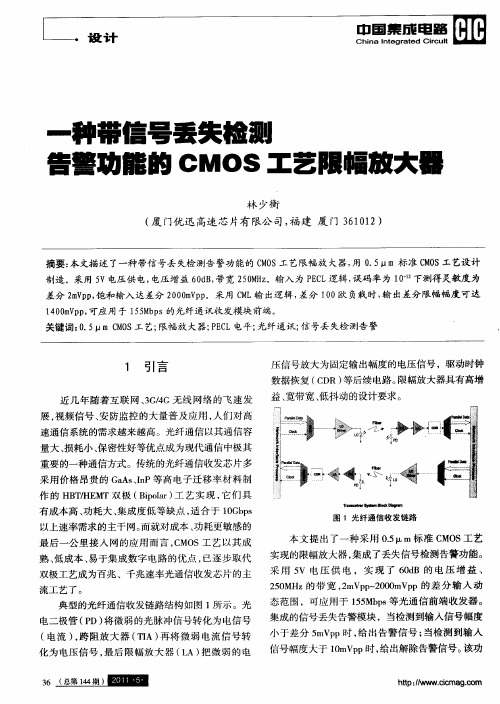
2 系统 框 图
本文 提 出 的 限 幅放 大器 系统 框 图如 图 2所 示 。 它 由输 入偏 置 、 增益 级 、 出缓 冲 、 流失 调 校准 、 输 直 信 号 丢失 检测 等模 块构 成 。输入 偏 置 f 莫块实 现将 输人
共模 电压偏 置 为 V C 1 V 的 P C C 一. 3 E L电平 , 并提 供差
h● ●^ .I^ …
^…
; …
能可 用来 检测 输入 信号 强度 是 否符 合要 求 ,可应 用
于光 通信 中的数字 诊断 功 能 。本 文 首先 描述 了限幅
放大 器 的系统 框 图 ,然 后对 各个 模块 的电路 设计 进 行 说 明 , 后展 示 了测试 结果 及 结论 。 最
测 模块 从增 益 级第 二级 取信 号 ,经过 全波 整流 电路
整 流后 输 入到 迟滞 比较 器进 行 比较输 。
分 1 0欧 的输入 阻抗 。为 了满足 增 益 、 宽要 求 , 0 带 以 及 抑制 共模 噪声 干扰 ,增 益 级采 用 多级全 差分 放 大 器 级 联 构 成 。为 了将 最 小 输 入 信 号 ( 敏 度差 分 灵 2 p 放 大 到 输 出 限 幅 幅 度 ( 分 10 m p , mV p) 差 4 0 V p)
中国联通WCDMA网络验收规范-核心网硬件验收分册

中国联通WCDMA网络验收规范核心网硬件验收分册中国联通集团移动网络公司2009年2月目录总则: (6)1:硬件安装检查 (10)H-01 硬件安装工程量的完成情况 (10)H-02 机架安装工艺检查项 (11)H-0201设备标签、相关标识检查 (11)H-0202 机架安装的检查 (11)H-0203 机架安装后的测试检查 (12)H-03 走线架及线槽的安装工艺检查项 (13)H-0301 支撑、吊挂,走线架和线槽安装的检查 (13)H-0302 非震区与震区的抗震加固检查 (14)H-0303 上走线、下走线的安装检查 (14)H-04 设备接地网检查项 (14)H-0401 防雷接地的检查 (14)H-0402 机架、终端、电源、配线架接地要求及线径检查 (16)H-0403 特殊情况接地检查 (16)H-05 电缆的布放工艺检查项 (17)H-0501 架间电缆的布放检查 (17)H-0502 直流电源电缆的布放检查 (18)H-0503 中继电缆的布放检查 (19)H-0504 网线的布放检查 (19)H-0505 光纤的布放检查 (20)H-06 机框和单板的安装检查项 (20)H-0601 机框的安装检查 (20)H-0602 单板的安装检查 (21)H-07 机台和外围终端设备的安装检查项 (21)H-0701 终端电缆的布放检查 (21)H-0702 终端设备的安装检查 (22)H-0703 告警箱的安装检查 (22)H-08 配线架的安装检查项 (23)H-0801 DDF/MDF架安装检查 (23)H-0802 ODF架安装检查 (23)H-09 电源模块、熔丝开关的安装检查 (24)H-0901电源模块、熔丝开关及标签的安装检查 (24)H-10隐蔽工程的检查项 (24)H-1001 电缆过孔洞、楼层时的隐蔽处检查 (24)H-11 供电检查 (24)H-1101 机架供电检查 (24)H-1102 机框供电检查 (25)H-1103 单板试通电检查 (25)2:MSC Server硬件测试验收 (25)SER-H-01单板测试 (25)SER-H-0101单板加载 (25)SER-H-0103单板倒换 (26)SER-H-02各单板、机框查询功能 (27)SER-H-0201各单板状态查询 (27)SER-H-0202各机框风扇状态查询 (27)SER-H-0203配电框的工作状态查询 (27)SER-H-0204各单版指示灯状态查询 (28)SER-H-03各输入/输出系统或后台设备的测试 (28)SER-H-04各处理模块的功能测试 (29)SER-H-05各通信物理端口的测试 (29)SER-H-0501单板测试 (29)SER-H-0502端口测试 (29)SER-H-06设备重启动测试 (30)SER-H-07IP出口设备测试 (30)3:MGW硬件测试验收 (31)MGW-H-01单板测试 (31)MGW-H-0101单板加载 (31)MGW-H-0102单板复位 (31)MGW-H-0103单板倒换 (31)MGW-H-02各单板、机框查询功能 (32)MGW-H-0201各单板、机框状态查询 (32)MGW-H-0202各机框风扇状态查询 (32)MGW-H-0203配电框的工作状态查询 (33)MGW-H-0204各单版指示灯状态查询 (33)MGW-H-03各输入/输出系统或后台设备的测试 (33)MGW-H-04各处理模块的功能测试 (34)MGW-H-05各通信物理端口的测试 (34)MGW-H-0501单板测试 (34)MGW-H-0502端口测试 (34)MGW-H-06设备重启动测试 (35)MGW-H-07IP出口设备测试 (35)4:HLR硬件测试验收 (36)HLR-H-01单板测试 (36)HLR-H-0101单板加载 (36)HLR-H-0102单板复位 (36)HLR-H-0103单板倒换 (37)HLR-H-02各单板、机框查询功能 (37)HLR-H-0201各单板状态查询 (37)HLR-H-0202各机框风扇状态查询 (37)HLR-H-0203配电框的工作状态查询 (38)HLR-H-0204各单版指示灯状态查询 (38)HLR-H-03各输入/输出系统或后台设备的测试 (39)HLR-H-04各处理模块的功能测试 (39)HLR-H-05各通信物理端口的测试 (39)HLR-H-07IP出口设备测试 (40)5:SGSN硬件测试验收 (41)SGSN-H-01单板测试 (41)SGSN-H-0101单板加载 (41)SGSN-H-0102单板复位 (41)SGSN-H-0103单板倒换 (41)SGSN-H-02各单板、机框查询功能 (42)SGSN-H-0201各单板、机框状态查询 (42)SGSN-H-0202各机框风扇状态查询 (42)SGSN-H-0203配电框的工作状态查询 (43)SGSN-H-0204各单版指示灯状态查询 (43)SGSN-H-03各输入/输出系统或后台设备的测试 (44)SGSN-H-04各处理模块的功能测试 (44)SGSN-H-05各通信物理端口的测试 (44)SGSN-H-06设备重启动测试 (44)SGSN-H-07IP出口设备测试 (45)6:GGSN硬件测试验收 (45)GGSN-H-01单板测试 (45)GGSN-H-0101单板加载 (45)GGSN-H-0102单板复位 (46)GGSN-H-0103单板倒换 (46)GGSN-H-02各单板、机框查询功能 (47)GGSN-H-0201各单板、机框状态查询 (47)GGSN-H-0202各机框风扇状态查询 (47)GGSN-H-0203配电框的工作状态查询 (47)GGSN-H-0204各单版指示灯状态查询 (48)GGSN-H-03各输入/输出系统或后台设备的测试 (48)GGSN-H-04各处理模块的功能测试 (49)GGSN-H-05各通信物理端口的测试 (49)GGSN-H-06设备重启动测试 (49)GGSN-H-07IP出口设备测试 (49)7:CG硬件测试验收 (50)CG-H-01物理端口测试 (50)CG-H-02 业务端口故障切换 (50)8:BG硬件测试验收 (51)BG-H-01物理端口测试 (51)9:NTP Server硬件测试验收 (51)NTP-H-01单板复位 (51)NTP-H-02单板查询 (51)NTP-H-03单板倒换 (51)NTP-H-04通信物理端口测试 (52)10:DNS硬件测试验收 (52)DNS-H-01系统CPU、内存、硬盘的利用率 (52)中国联通WCDMA网络验收规范(核心网硬件验收分册)总则:本规范规定了WCDMA核心网交换设备的硬件验收规范,核心网网元的硬件验收分册包括两部分:硬件安装检查和网元的相应硬件测试部分。
【电子技术应用】_科研_期刊发文热词逐年推荐_20140727
科研热词 高峰 重复控制 逻辑分析仪 逆变器 辐射测温 跟踪 误差分析 论坛 视觉定位 虚拟仪器 蓝牙技术 蓝牙开发平台 节能与环保 红外 粒子滤波器 目标分割 电源 瓦斯浓度 热超声倒装 热电探测器 点目标 漏磁检测 温度传感器 气体传感器 杂志社 星敏感器 星图 无线通信 无线传感器网络 数据融合 数据传输 数字图像处理 序列图像 并网 小波去噪 实时监控 定向洪泛 多用户检测 多传感器技术 图像目标识别 国际 合法侦听 功率控制 分布式系统 分布式油田 光学辐射 光伏系统 产品设计 产业发展 中国电子 专业委员会 sip
抗干扰 手指静脉图像 成品率 建模仿真 应急指挥 嵌入式控制系统 嵌入式技术 小波域 小数分频 定位系统 安全警示 大型设备 大型机械设备 多重音频水印 多媒体服务质量 声达时间差 地质灾害 图像编码 压电陶瓷 单片机 区分服务 动态自校正 剪切攻击 分形 傅里叶分析 信息化 信号频率的微调 低信噪比 优先级置顶 优先级继承 优先级反转 人防工程 人体阻抗网络 乘积合并 两轴模拟mems陀螺仪 两化 三维地理信息系统 wdm picoblaze mt8870 mcp2515 matlab mas mapxtreme mac协议 imaodv gps dtmf dds cy7c68013 cmos图像传感器 cc2420 can总线 atmega128单片机
推荐指数 3 2 2 2 2 2 1 1 1 1 1 1 1 1 1 1 1 1 1 1 1 1 1 1 1 1 1 1 1 1 1 1 1 1 1 1 1 1 1 1 1 1 1 1 1 1 1 1 1 1 1 1
2011年 序号 1 2 3 4 5 6 7 8 9 10 11 12 13 14 15 16 17 18 19 20 21 22 23 24 25 26 27 28 29 30 31 32 33 34 35 36 37 38 39 40 41 42 43 44 45 46 47 48 49 50 控实验台 逆系统 达林算法 软测量 软件无线电 转子磁链定向的矢量控制 误符号率 自适应量化 空间谱估计 禁忌搜索 电压无功优化 波达方向(doa) 油门控制器 永磁同步电动机 正交空时分组码 无线控制 数据加密 数字音频水印 数字视频 数字波束形成 数字中频接收机 数字下变频 支持向量机 执行器 心理声学模型 嵌入式软plc 嵌入式系统 射频识别 字符型虚拟机 多任务实时操作系统 同步信号 反馈控制 加密技术 功率放大器 伺服控制系统 仿真优化 下位机系统 一维弹道修正 windows ce usb接口 rfid信号 pid控制 mimo mgf gprs fpga c++ arm aes算法
ICDPPCNEXUS MPC55xx MPC56xx In-Circuit Debugger
ICDPPCNEXUSMPC55xx / MPC56xx In-Circuit DebuggerQuick Start GuideCopyright 2009, P&E Microcomputer Systems, Inc. All rights reserved.Visit us on the web at Document Version HistoryVersion Date Notes1.0 21 Sep 2009 Initial versionCONTENTS1 Introduction (4)1.1 P&E Compatible Hardware (4)2 Getting Started (5)2.1 Connecting to your Target (5)2.2 Reset Script (6)2.3 Loading Data and Debug Information (7)2.4 CPU and Memory Windows (8)3 Debugging (10)3.1 GOTIL command (10)3.1 Stepping through C instructions (11)3.3 Setting and Reaching Breakpoints (12)3.4 Using Code Window Popup Debug Evaluation Hints (13)3.5 Using the Variables Window (15)3.6 Modifying a Variable (16)3.7 Using the Register Interpreter (17)3.8 Adding Register Field Descriptions to the Variables Window (20)1 IntroductionThis document is a step-by-step guide to using the P&E ICDPPCNEXUS in-circuit debugger software, which is compatible with Freescale MPC55xx / MPC56xx processors. This guide covers the most commonly used features of the debugger: loading binary & debug information, accessing CPU registers & memory, stepping code, setting breakpoints, and monitoring variables.1.1 P&E Compatible HardwareThe following lists the P&E hardware compatible with the ICDPPCNEXUS debugger software.P&E Part Number Interface to host PCCABPPCNEXUS Parallel (LPT) portUSB-ML-PPCNEXUS USB 2.0 (Backwards compatible with USB 1.1 ports) Cyclone MAX Serial (RS232) portUSB 1.1 (Upwards compatible with USB 2.0 ports)Ethernet2 Getting Started2.1 Connecting to your TargetUpon starting the debugger, the connection assistant dialog appears:•Use the “Interface” and “Port” drop-down menus to choose the P&E hardware interface connected between the PC and your target board.•The “Target CPU” setting can safely be left at the “Autodetect” setting for most users. If you experience problems connecting, you can try specifying the exact Freescale device that you are connecting to.• A BDM_SPEED parameter between 2 to 4 can typically be used.Processors running at slower clock speeds will require higher values.Click the Connect button, and ICDPPCNEXUS will attempt to contact the processor. Using the default debugger settings, ICDPPCNEXUS will establish communications and reset the processor.After establishing communications, the main debugger screen will appear, and a debugger reset script macro should automatically execute and complete.2.2 Reset ScriptThis section explains the initialization that the debugger, using a reset script macro file, performs on the processor. The user can view and modify all of the macro file's initialization tasks.The processor Boot Assist Module (BAM) would normally initialize the memory of the processor. However, when running the target application from the debugger, the BAM functionality is disabled. To account for this, the debugger must run a script file on reset. The script initializes the memory of the processor similar to the way in which the BAM would initialize the processor.If ICDPPCNEXUS is launched from the Freescale CodeWarrior IDE, the correct reset script file is automatically selected.If ICDPPCNEXUS is launched stand-alone, the reset script file may need to be configured. Several reset script macros are included with the ICDPPCNEXUS debugger and have a .mac extension. For detailed information, you can view each macro file using a simple text editor such as Notepad. The macro contents will contain useful comments, such as which devices are supported by that particular macro.To configure the debugger reset script macro, select the debugger Configuration menu, Automated Script Options dialog, shown here:2.3 Loading Data and Debug InformationIf ICDPPCNEXUS is launched from the Freescale CodeWarrior IDE, your code will automatically be downloaded to the processor.•RAM projects are loaded into the processor’s internal SRAM.•FLASH projects will invoke the CPROGPPCNEXUS Flash programming software to burn the code into the processor’s internal FLASH.The debug information is also automatically loaded from CodeWarrior, which will allow you to debug using your high level source code and variables.If ICDPPCNEXUS is launched stand-alone, you will need to manually download the code and debug information. Launch the Load Dialog by clicking on the High Level Load button on the debugger tool bar:This dialog allows you to specify the binary/debug file and whether to load into RAM or FLASH. Once you are satisfied with your settings, press the “Process Load Command” button to begin the download process. This step will also load the debug information.2.4 CPU and Memory WindowsThe CPU Window displays all CPU core registers, including the Program Counter (PC) and all general purpose registers.•To modify CPU register contents, double-click the register value. You will be prompted for a new value.The Memory Window displays data at any given memory address. It can be used to view RAM contents, FLASH contents, and values of peripheral registers.•To change the memory address, right-click inside the Memory Window and select “Set Base Address”. You will be prompted for a new address to begin displaying data.•To change the contents in memory, double-click the value in memory that you would like to change. You will be prompted for a new value.3 DebuggingThis section outlines the different debugging capabilities available in the ICDPPCNEXUS debugger once the debug information has been loaded.3.1 GOTIL commandAt this point, your source window will show the assembly language startup code generated by the compiler:If you do not need to debug this section and would like to run the processor until the beginning of your “main” function, you can use the “GOTIL” command.•Type “GOTIL main” in the Status window to tell the debugger to run code until it reaches the “main” function of your code.The “GOTIL” command works with any function in your code.3.1 Stepping through C instructionsStep through the initialization code, or any source code, using the high-level language source step command. Use this feature by typing “HSTEP” in the Status window or by clicking the high-level step button on the debugger tool bar:Each time the HSTEP command executes, the debugger will rapidly single step assembly instructions until it encounters the next source instruction, at which point target execution will cease. When the debugger reaches the next source instruction, all visible windows will be updated with data from the board. After reaching the main function, step through several C language instructions. Notice that some instructions will take longer to step through than others because each C instruction may consist of a greater or fewer number of underlying assembly instructions.3.3 Setting and Reaching BreakpointsIn the source code window, there will be a small red dot and a small blue arrow next to each source instruction that has underlying object code. If a large blue arrow appears on a source line, this indicates that the program counter (PC) currently points to this instruction. If a large red stop sign appears on the source line, this indicates that a breakpoint exists on this line.•Set a breakpoint at an instruction by double-clicking the tiny red dot.•To remove a breakpoint, double-click the large red stop sign.Execution will begin in real-time when you issue the HGO command or click the high-level language GO button on the debugger tool bar:If the debugger encounters a breakpoint, execution will stop on this source line. If it does not encounter a breakpoint, target execution will continue until you press a key or use the stop button on the debugger tool bar:•By double clicking the small blue arrow, you will be issuing a GOTIL command to the address of this source line.A GOTIL command will set a single breakpoint at the desired address, and the processor will begin executing code in real-time from the current program counter (PC). When the debugger encounters the GOTIL address, execution stops. If the debugger does not encounter this location, execution continues until you press akey or use the stop button on the debugger tool bar. Note that all user breakpoints are ignored when the GOTIL command is used.You may also double-click the red and blue symbols in the disassembly window. The disassembly window may display an additional symbol, a small, blue "S" enclosed in a box. This indicates that that a source code instruction begins on this disassembly instruction.3.4 Using Code Window Popup Debug Evaluation HintsWhen debugging source code, it is convenient to view the contents of a variable while viewing your source code. The in-circuit debugger has a feature, debug hints, which displays the value of a variable while the mouse cursor is held over the variable name. The hint may be displayed in any of three locations, as shown below.The three locations for the debug hints are the code window title bar, the status window caption bar, and a popup hint that appears over the variable in source code. You can configure the hints to display in any combination.•Set the locations of debug hints in the configuration menu of the debuggerThe information in the popup hint box is similar to the information displayed in the variables window.The information includes the variable name (i), value ($1), and type (signed long).3.5 Using the Variables WindowThe variables window displays the current value of application variables. The following window shows a display of variables from the example application.Variables that are pointer or reference types are displayed in red. Normal variables are displayed in black.•Add a variable by typing the VAR command, by right clicking the variables window and choosing “Add a variable”, or by hitting the "Add Variable"button in the variables window.When adding a variable using the pop-up menu, the debugger displays the following screen.In the variable field, type the address or name of the variable. Typically, set the type of the variable to “Default”, which means that the variable will be displayed as it is defined in the debugging information. When adding a variable, you may specify the numeric display base of the variable.3.6 Modifying a Variable•To modify the current value of a variable, right-click the variable name in the variables window and select “Modify Variable” to display a dialog.Check the “Modify value” checkbox, and type the variable’s new value. After you click the OK button, the debugger updates the variable value on the target, and the debugger refreshes the variable window to display the new value. Note that the debugger will not edit certain user-defined types, such as enumerated types.•You may also modify a variable’s display properties, such as the type or numeric display base using this dialog.3.7 Using the Register InterpreterThe register interpreter provides a descriptive display of bit fields within the processor’s peripheral registers. The register interpreter allows you easily to change the value of these registers. You may quickly check the current state of a peripheral and examine the configuration of the target device.When you use the register interpreter within the debugger, it reads the current value of the peripheral register, decodes it, and displays it.To launch the register interpreter in the debugger, either use the “R” command or click the view/edit register button on the tool bar:A window will appear that allows you to select a peripheral block to examine.Double clicking the module of choice will launch the register selection window.Double clicking a specific register will launch the edit/display window for that register.The window lists the keystrokes and mouse actions, allowing you to modify the values of each of the fields. After right clicking on a specific field, the register interpreter will display all options for that field.When you quit the register view/edit window by hitting the ESC key, you will be given the opportunity to write the new value into the register, as shown in the following window.3.8 Adding Register Field Descriptions to the Variables WindowAdd register bit fields to the variables window by using the “_TR” command in the debugger or by clicking the "Add Register" button in the variables window. After selecting the register field, the field appears in the debugger variables window, and the debugger will continually update its value.。
原理图
VCC
C23 104
C22 104
C8 104
RP5B
DSIO P34
Relay: 继电 器接 口 BEEP:蜂 鸣器接口
C21 GND PY1.2 PY1.1 PY1.0 PY1.3 Relay BEEP C4 16 15 14 13 12 11 10 U17 OUT1 OUT2 OUT3 OUT4 OUT5 OUT6 OUT7 104 IN1 IN2 IN3 IN4 IN5 IN6 IN7 GND VCC ULN2003D
复 位电 路
JP9 P1.1
1 2
上 拉电 阻
RP6 4 3 2 1 4 3 2 1 P16 P17 P32 P33
10K*8
上 拉电 阻
P1.3
继电器
RP7
(E EPR OM)与(模数/数模 转换)
AOUT: 数模 输出 AIN0-AIN3: 模拟 输入
U7 VCC 16 14 GND 13 12 11 VCC VREF AGND EXT OSC SCL SDA PCF8591P AOUT AIN0 AIN1 AIN2 AIN3 A0 A1 A2 GND 15 AOUT 1 2 3 4 5 6 7 8 GND AIN0 AIN1 AIN2 AIN3 GND AIN0 R28 1K J4 1 2 3 4 5 6 1 2 3 4 DA
U13 D0 D1 D2 D3 D4 D5 D6 D7 Q0 Q1 Q2 Q3 Q4 Q5 Q6 Q7 19 18 17 16 15 14 13 12 R20 R21 100R R22 R23 R24 R25 R26 R27 D11 D12 D13 D14 D15 D16 D17 D18
OE VCC LE GND 74573
OV系列单芯片CMOS摄像机中文资料
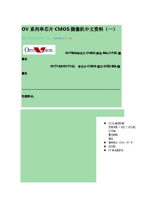
电视机,视频监视器和其他75欧姆终端输入的视频设
备。OV7910 / OV7410 / OV7411视频摄像机是低功耗设
计,仅需要5V 直流供电。这两个产品非常合适于小体
感光阵列
NTSC:510*492像素
PAL:628*582像素
靶面尺寸
NTSC:4.69*3.54毫米
PAL:5.78*4.19毫米
单芯片1/3英寸
视频摄像机
全电视信号输
出:NTSC/ PAL 或
S-视频
分量电视信号
输出:RGB 或 YUV
灵敏度提升
(+18Db)/ AGC
关闭时
自动暴光控制
/ 自动增益控制/
自动白平衡
外部桢同步输
入
孔阑校正
视频会议
可视电视
视频电子邮件
PC 电脑眼 玩具 保安监视 医疗仪器 汽车尾视
VTO-P 视频峰值电平
-
2.3
2.4
-
VTO-B 视频黑电平
-
0.7
1.2
-
VSYNC 视频同步脉冲
-
0.7
0.4
-
幅度
RO 视频输出负载
75
75
单位
V V V Ohm
2. SCCB 总线 OV7910/OV7410/OV7411中的许多功能是设置寄存器都可以通过 SCCB 高
速 串行接口操作。通过将 SBB 管脚(管脚34)和 VDD 之间一个10K 电阻,即可 允许 SCCB 接口。当 SCCB 操作允许时(SBB=1),OV7910/OV7410/OV7411 图像传感器就以从设备方式工作,支持7位地址/数据和400K 位/秒的串行传输 速度。每一个字节,第一位是最高位,读写控制位是第一字节的最低位。协议
EMC、光纤交换机及服务器配置过程总结

EMC、光纤交换机及服务器配置过程总结-----------------------作者:-----------------------日期:更多资料请访问.(.....)EMC、光纤交换机及服务器配置过程总结目录版本记录1概述本文主要从实用的角度整个描述EMC的划分、光纤交换机的配置以及服务器的设置,最终实现SAN环境中服务器成功分配EMC空间。
首先我们在光纤交换机上定义一些通道即zone,允许服务器与EMC通讯;其次EMC能够识别到服务器并将EMC空间划分给服务器;最后服务器成功识别到EMC划分的空间。
本文按照配置顺序对于配置过程中的步骤一一描述:本文配置过程背景:p550DB、mttest、gfstest1、gfstest2四台服务器需要通过光纤交换机连接EMC,p550DB、mttest能且只能访问EMC分配的独立空间;gfstest1、gfstest2也能能且只能够访问EMC划分的独立空间。
2光纤交换机配置2.1 现有光纤交换机信息现有SAN网络中使用光纤交换机两台,具体信息如下:2.1.1sw012、端口物理连接如下:2.1.2Sw02交换机型号EMC Conectrix DS16B3,端口物理连接如下:2.1.3设备连接汇总表2.2 光纤交换机配置2.2.1术语配置Zone需要涉及到三个对象的配置Alias,Zone,Configuration:Alias可以把设备的WWN或Domain,Port声明为Alias,用于更好更直观的标示设备;同时当Zone中的某个成员更换时,如果定义了Alias,只要修改Alias的定义就可以调整Zone 中的成员,而不用修改Zone的配置。
Zone区域,Zone内的设备可以相互访问,但不能访问其他Zone的设备;Zone的成员可以有三种:“Domain,Port”;”WWN”;”Alias”;Configuration在交换机上的一套关于Zone的配置,或者说一系列Zone的集合。
CC110x CC111x OOK ASK Register Settings说明书

CC110x/CC111x OOK/ASK Register SettingsBy Sverre HellanKeywordsOOKASKPER (Packet Error Rate)CC1100CC1100ECC1101CC1110CC1111CC4301 IntroductionThis design note provides guidelines forfinding optimum register settings forOOK/ASK operation. The starting point forthe optimization is the preferred settingsgiven by the SmartRF®Studio SW. Theuser needs to measure the sensitivity(PER) over the full input dynamic range todetermine the optimum settings.This design note uses CC1101 as anexample on how to find optimum registersettings, but it is also applicable forCC1100, CC1100E, CC1110, CC1111,and CC430.Table of ContentsKEYWORDS (1)1INTRODUCTION (1)2ABBREVIATIONS (2)3OOK/ASK REGISTER SETTINGS (3)3.1AGC S ETTINGS (3)3.2IF F REQUENCY (4)3.3P ROCEDURE FOR F INDING OOK/ASK S ETTINGS USING S MART RF®S TUDIO (5)4GENERAL INFORMATION (8)4.1D OCUMENT H ISTORY (8)2 AbbreviationsAGC Automatic Gain ControlASK Amplitude Shift KeyingEM Evaluation Module2-FSK Frequency Shift KeyingGFSK Gaussian shaped Frequency Shift KeyingIF Intermediate FrequencyMSK Minimum Shift KeyingOOK On-Off KeyingPER Packet Error RateSW Software3 OOK/ASK Register Settings3.1 AGC SettingsThe register settings provided by SmartRF®Studio have been optimized for 2-FSK/GFSK/MSK modulation and when using one of the preferred settings and only changing the modulation format to OOK/ASK, the AGC settings might result in unstable or non-optimum reception (i.e. degraded sensitivity). This is pictured in Figure 1.Figure 1. Example of Unstable, Non-Optimum, and Optimum ReceptionThe optimum AGC settings change with RX filter bandwidth and data rate, but for OOK/ASK the following has been found to give good results:AGCCTRL2 = 0x03 to 0x07AGCCTRL1 = 0x00AGCCTRL0 = 0x91 or 0x92In the example shown in Figure 2, the best sensitivity is achieved with AGCCTRL2 = 0x04, AGCCTRL1 = 0x00, and AGCCTRL0 = 0x92. Please note that optimum register settings change with data rate so it is important to measure sensitivity for different combinations of AGCCTRL2 and AGCCTRL0. Furthermore, as shown in Figure 1, some combinations of AGC settings results in unstable reception. That is, for some input power levels above the sensitivity limit there will be degraded packet error rate (PER). It is therefore important to check the PER for the entire dynamic range and not only at the sensitivity limit. One option is to check the PER for every 2 dB increase in input power level.AGCCTRL2.MAGN_TARGET[2:0] is used to set an on-chip target value for the peak signal amplitude. MAGN_TARGET is used by the AGC loop to set the correct gain.AGCCTRL0.FILTER_LENGTH[1:0] is used to configure the ASK decision boundary. If the ASK decision boundary is set to 8 dB, the “low” bit must be at least 16 dB below the “high” bit.Figure 2. PER versus Input Power Level for Different AGC Register Settings (3.8 kBaud,100 kHz RX Filter Bandwidth) 3.2IF FrequencyRegister FSCTRL1 sets the IF frequency and the optimum value is different for different RX filter bandwidths. It is therefore recommended to find the FSCTRL1 setting using one of thepreferred RX filter bandwidth settings in SmartRF ®Studio (see Figure 3). If the wanted RX filter bandwidth is not given by one of the preferred settings, choose the FSCTRL1 setting for the first RX filter bandwidth that is wider than the wanted RX filter bandwidth.As an example, for a wanted 150 kHz RX filter bandwidth use the FSCTRL1 setting given for 232 kHz RX filter bandwidth.RX filter bandwidthsused by preferred settings:58 kHz, 100 kHz, 232 kHz, 325 kHz, 540 kHz, 812 kHzFigure 3. Available RX Filter Bandwidths Given by the Preferred Settings in SmartRF ®StudioNote that the FREND1, FIFOTHR, TEST2, and TEST1 register settings change for different RX filter bandwidths.FREND1:RX filter bandwidth > 101 kHz, FREND1 = 0xB6RX filter bandwidth ≤ 101 kHz, FREND1 = 0x56TEST2:RX filter bandwidth > 325 kHz, TEST2 = 0x88RX filter bandwidth ≤ 325 kHz, TEST2 = 0x81TEST1:RX filter bandwidth > 325 kHz, TEST1 = 0x31RX filter bandwidth ≤ 325 kHz, TEST1 = 0x35FIFOTHR:RX filter bandwidth > 325 kHz, FIFOTHR = 0x07RX filter bandwidth ≤ 325 kHz, FIFOTHR = 0x473.3 Procedure for Finding OOK/ASK Settings using SmartRF® StudioAs an example, assume 4.8 kBaud data rate and 203 kHz RX filter bandwidth.1) Use SmartRF®Studio to find the optimum IF frequency. Select the preferred setting that has an RX filter bandwidth equal to the wanted bandwidth. If the wanted RX filter bandwidth is not given by one of the preferred settings, chose the first RX filter bandwidth that is wider than the wanted bandwidth. For a 203 kHz wanted RX filter bandwidth, select the 232 kHz RX filter bandwidth for optimum IF frequency.2) Change the data rate and the RX filter bandwidth to the wanted values. Change the modulation format to ASK/OOK. Press “Reset CC1101 and write settings” (if SmartRF® Studio is being used to control a CC1101EM) and then “Copy settings to Register View”3) In Register View, change the AGCCTRL2, AGCCTRL1, and AGCCTRL0 settings as explained in Section 3.1. Make sure the FSCTRL1, FIFOTHR, FREND1, TEST2, and TEST1 registers are set as explained in Section 3.2. It is possible to print the register settings to a file using “Export CC1101 Registers” under “File”.Press the “Write” butt on for the register to be updated if SmartRF® Studio is being used to control a CC1101EM.4) If SmartRF ®Studio is being used to perform the test, go back to Normal View. Check the Manual Init box for the changes done in Register View to take effect.4 General Information4.1Document HistoryIMPORTANT NOTICETexas Instruments Incorporated and its subsidiaries(TI)reserve the right to make corrections,modifications,enhancements,improvements, and other changes to its products and services at any time and to discontinue any product or service without notice.Customers should obtain the latest relevant information before placing orders and should verify that such information is current and complete.All products are sold subject to TI’s terms and conditions of sale supplied at the time of order acknowledgment.TI warrants performance of its hardware products to the specifications applicable at the time of sale in accordance with TI’s standard warranty.Testing and other quality control techniques are used to the extent TI deems necessary to support this warranty.Except where mandated by government requirements,testing of all parameters of each product is not necessarily performed.TI assumes no liability for applications assistance or customer product design.Customers are responsible for their products and applications using TI components.To minimize the risks associated with customer products and applications,customers should provide adequate design and operating safeguards.TI does not warrant or represent that any license,either express or implied,is granted under any TI patent right,copyright,mask work right, or other TI intellectual property right relating to any combination,machine,or process in which TI products or services are rmation published by TI regarding third-party products or services does not constitute a license from TI to use such products or services or a warranty or endorsement e of such information may require a license from a third party under the patents or other intellectual property of the third party,or a license from TI under the patents or other intellectual property of TI.Reproduction of TI information in TI data books or data sheets is permissible only if reproduction is without alteration and is accompanied by all associated warranties,conditions,limitations,and notices.Reproduction of this information with alteration is an unfair and deceptive business practice.TI is not responsible or liable for such altered rmation of third parties may be subject to additional restrictions.Resale of TI products or services with statements different from or beyond the parameters stated by TI for that product or service voids all express and any implied warranties for the associated TI product or service and is an unfair and deceptive business practice.TI is not responsible or liable for any such statements.TI products are not authorized for use in safety-critical applications(such as life support)where a failure of the TI product would reasonably be expected to cause severe personal injury or death,unless officers of the parties have executed an agreement specifically governing such use.Buyers represent that they have all necessary expertise in the safety and regulatory ramifications of their applications,and acknowledge and agree that they are solely responsible for all legal,regulatory and safety-related requirements concerning their products and any use of TI products in such safety-critical applications,notwithstanding any applications-related information or support that may be provided by TI.Further,Buyers must fully indemnify TI and its representatives against any damages arising out of the use of TI products in such safety-critical applications.TI products are neither designed nor intended for use in military/aerospace applications or environments unless the TI products are specifically designated by TI as military-grade or"enhanced plastic."Only products designated by TI as military-grade meet military specifications.Buyers acknowledge and agree that any such use of TI products which TI has not designated as military-grade is solely at the Buyer's risk,and that they are solely responsible for compliance with all legal and regulatory requirements in connection with such use. TI products are neither designed nor intended for use in automotive applications or environments unless the specific TI products are designated by TI as compliant with ISO/TS16949requirements.Buyers acknowledge and agree that,if they use any non-designated products in automotive applications,TI will not be responsible for any failure to meet such requirements.Following are URLs where you can obtain information on other Texas Instruments products and application solutions:Products ApplicationsAudio /audio Automotive and Transportation /automotiveAmplifiers Communications and Telecom /communicationsData Converters Computers and Peripherals /computersDLP®Products Consumer Electronics /consumer-appsDSP Energy and Lighting /energyClocks and Timers /clocks Industrial /industrialInterface Medical /medicalLogic Security /securityPower Mgmt Space,Avionics and Defense /space-avionics-defense Microcontrollers Video and Imaging /videoRFID OMAP Mobile Processors /omapWireless Connectivity /wirelessconnectivityTI E2E Community Home Page Mailing Address:Texas Instruments,Post Office Box655303,Dallas,Texas75265Copyright©2012,Texas Instruments Incorporated。
Dell EqualLogic PS4100 存储阵列 安装和设置指南说明书
安装安全预防措施
请遵循这些安全预防措施: • Dell 建议仅让具有机架安装经验的人员在机架中安装阵列。 • 请确保阵列在任何时候都完全接地,以防止静电释放所带来的损坏。 • 处理阵列硬件时,请务必使用阵列随附的防静电腕带或采用类似的防护措施。 • 至少需要两个人将阵列机箱抬出包装箱。
表 1: 包装箱内物品
说明 PS Series 4100 阵 列 包 含 : • 一 个 或 两 个 类 型 12 控 制 模 块 • 两个电源设备和冷却模块 PS4100 包 含 最 多 12 个 3.5 英 寸 或 24 个 2.5 英 寸 串 行 连 接 SCSI (SAS) 驱 动 器 ,取 决 于 型 号后缀。
注 : 如果您无法访问互联网,则可通过发票、装箱单、单据或 Dell 产品目录找到联系信息。
v
安装和设置指南
前言
如果对销售、技术支持或客户服务存有疑问而需联系 Dell,则应遵循以下步骤: 1. 访问 或 Dell 产品随附信息中指定的 Dell 支持 URL。 2. 选择您的地区。使用地区菜单或单击指定您所在国家/地区或区域的链接。 3. 选择所需服务。单击 Contact Us( 联系我们) 链接,或从提供的服务列表中选择 Dell 支持服务。 4. 选择您首选的 Dell 支持联系方式,如电子邮件或电话。
夹连接到接地设备。正确的接地设备示例为 ESD 垫,或设备接地部件的金属框架。
包装箱内物品和所需硬件
确保包装箱中含有如表 1 中所述的所有物品。对于包装箱中未包含但特定环境必需的其他硬件, 您需要自行提供。请参见表 2。
4
安装和设置指南
2 用机架安装阵列
华为S3528_S3552版本升级
华为S3528_S3552版本升级作者:古月日期:2009-02-16 QQ:30555006查看S3528_S3552-VRP310-R0031P10的软件版本和Bootrom版本号方式如下:<Quidway> display versionHuawei Versatile Routing Platform SoftwareVRP Software, Version 3.10, Release 0031P10 ------- 注①Copyright (c) 1998-2008 Huawei Technologies Co., Ltd. All rights reserved.Quidway S3552G uptime is 0 week,0 day,0 hour,1 minuteQuidway S3552G with 1 MPC 8241 Processor64M bytes DRAM16384K bytes Flash MemoryConfig Register points to FLASHHardware Version is REV.CCPLD Version is CPLD 003Bootrom Version is 207 ------ 注②[Subslot 0] 48FE Hardware Version is REV.C[Subslot 1] 4GE Hardware Version is REV.0网络管理人员在本地计算机上运行FTP Server,注意配置文件所在目录正确(假设IP地址为10.10.10.1),Telnet远程登录到交换机上,利用FTP将主机程序传送到交换机上,假设主机程序为S3552.app,BOOTROM程序为S3552.btm,在用户视图下执行:ftp 10.10.110.1Trying ...Press CTRL+K to abort Connected.220 WFTPD 2.0 service (by Texas Imperial Software) ready for new userUser(none):lyt331 Give me your password, please Password:230 Logged in successfully[ftp] get S3552.app S3552.app[ftp] get S3552.btm S3552.btm[ftp] bye<Quidway> boot bootrom S3552.btmplease wait ...Bootrom is updated!<Quidway> boot boot-loader S3552.app<Quidway> display boot-loaderThe app to boot at the next time is: flash:/S3552.app <Quidway> reboot。
V-DOSC MANUAL V4 0605 1-50

L-ACOUSTICS V-DOSC Manual Version 4
6/29/2005
Page 4 of 158
TABLE OF CONTENTS
TABLE OF CONTENTS........................................................................................................................... 5 LIST OF FIGURES.................................................................................................................................... 8 LIST OF TABLES ....................................................................................................................................10 INTRODUCTION .................................................................................................................................. 11 WAVEFRONT SCULPTURE TECHNOLOGY FUNDAMENTALS ........................................................ 11 THE SOUND REINFORCEME
【CN110460746A】用于具有行标记存储器的非对称图像分割器的系统和方法【专利】
(19)中华人民共和国国家知识产权局(12)发明专利申请(10)申请公布号 (43)申请公布日 (21)申请号 201910374460.3(22)申请日 2019.05.07(30)优先权数据62/668,087 2018.05.07 US16/381,408 2019.04.11 US(71)申请人 马克西姆综合产品公司地址 美国加利福尼亚州(72)发明人 Y ·巴尔希欧格鲁 A ·K ·巴佛拉 L ·雅克 (74)专利代理机构 永新专利商标代理有限公司72002代理人 张伟 王英(51)Int.Cl.H04N 5/222(2006.01)H04N 5/262(2006.01)G06T 7/11(2017.01)G06T 1/60(2006.01) (54)发明名称用于具有行标记存储器的非对称图像分割器的系统和方法(57)摘要本文描述了提供用于实施可以降低存储器要求的非对称图像分割器引擎的系统和方法。
在一个或多个实施例中,一种方法可以包括接收包括超帧视频图像的多流传输视频,其中,每个超帧视频图像包括第一视频图像和第二视频图像,并且其中,所述第一视频图像的高度高于所述第二视频图像。
通过向所述第二视频图像添加填充,可以将所述第二视频图像的竖直非对称性调整到与所述第一视频图像相同的高度。
可以利用非对称图像分割器引擎来将所述超帧视频图像分割成两个分离的视频图像。
通过使用行标记存储器来标记所述第二视频图像的每一行,可以确定哪些行被填充和丢弃、和哪些行是要显示的数据。
权利要求书2页 说明书9页 附图8页CN 110460746 A 2019.11.15C N 110460746A权 利 要 求 书1/2页CN 110460746 A1.一种方法,包括:接收包括超帧视频图像的多流传输视频,其中,每个超帧视频图像包括第一视频图像和第二视频图像,并且其中,所述第一视频图像的高度高于所述第二视频图像;通过向所述第二视频图像添加填充来将所述第二视频图像的竖直非对称性调整到与所述第一视频图像相同的高度;利用被配置为将所述超帧视频图像分割成两个分离的视频图像的非对称图像分割器;以及使用行标记存储器来标记所述第二视频图像的每一行,以确定哪些行被填充和丢弃、和哪些行是要显示的数据。
- 1、下载文档前请自行甄别文档内容的完整性,平台不提供额外的编辑、内容补充、找答案等附加服务。
- 2、"仅部分预览"的文档,不可在线预览部分如存在完整性等问题,可反馈申请退款(可完整预览的文档不适用该条件!)。
- 3、如文档侵犯您的权益,请联系客服反馈,我们会尽快为您处理(人工客服工作时间:9:00-18:30)。
3. Implemented an NPU solution, but:
10G
Programmable Headroom
SDRAM SDRAM
SDRAM
SDRAM
6/18/2014
© IDT CONFIDENTIAL
PAGE 7
Accelerated Thinking
TM
IL-PSC Offload by Application
NPU or ASIC/FPGA
• Ethernet Bridging • VLAN • IPv4 • IPv6 • MPLS • SLA Enforcement
IL-PSC: Functional View
Internal Tables & Statistics Database Aging Acceleration
Search Engines
SPI 4.2 Input (400 MHz)
Packet Assembly
Recursive Packet Parser
Accelerated Thinking
TM
பைடு நூலகம்
6/18/2014
© IDT CONFIDENTIAL
PAGE 9
Data Flow Diagram
Packet In
Packet Rx Port
Control Plane In
Packet Memory Packet Parser Search Control Packet Editor
Inexpensive Programmable Line Rate Offload for Complex Packet Classification and Header Processing
6/18/2014 © IDT CONFIDENTIAL PAGE 3
Accelerated Thinking
Packet Out
Accelerated Thinking
TM
PSC Linecard Architectures
TCAM SRAM SRAM
Classifier
ASIC / FPGA / NPU
MAC / Framer
Fabric
6/18/2014
PHY PHY PHY
TM
CostReduction
Issues
– – – – – Doesn't scale Not inherently secure No Direct QoS support Not Resilient Disruptive
Solutions
– Stacked VLANs / MPLS / VPLS for Scalability – Prioritization for CoS / QoS – Data tunneling for security – Programmability for Timeto-Market improvement
6/18/2014 © IDT CONFIDENTIAL
Associated Data SDRAM (333 MHz) PAGE 11
External Stats SDRAM (333 MHz)
Accelerated Thinking
SPI 4.2 Output (400 MHz)
TM
Expansion
15 Mpps 82 Byte Packets
• Integrated Search Engines for Classification, Filtering Support • Recursive Search Capability
– Build and recursively apply up to 4 keys per packet @ line rate
Meter it ?
Count it ?
Traffic Manager
Typical Packet Processing Functionality PSC Functionality Partial PSC Functionality
6/18/2014 © IDT CONFIDENTIAL PAGE 4
Packet / Result Out
Packet Tx Port
Search Result Up to 4x Key: 32 - 320 bits Handle Assoc. Data (up to 256 bits)
Payload
Payload
Handle (Index) Assoc. Data
10G Classification 10G ACL Filtering Policing State Processing Packet Editing Customer Differentiation <10G Congestion Avoidance Shaping <10G
SDRAM SDRAM TCAM
Recursive Search Control
Packet Editor
Processor Array (x 64 Threads) Packet Insertion Extraction
External Tables & Statistics I/F
Packet Buffer
PCI Interface (32 x 66 MHz)
– Transition to an NPU is risky, expensive – Want a simple, fast, inexpensive programming environment
2. Modifying an existing FPGA / ASIC solution, but:
Packet Processing Features
Typical resource budgets per packet for Ethernet applications are shown in this table
Function
Exact Match searches (<= 128 bit) TCAM searches (<= 160 bit) Assoc. Data reads OR writes (120 bit) Max. Associated Data writes (120 bit) Off-chip Stats counter updates Local SRAM accesses (128 bit) Packet modifications (1-16 Byte updates) Max. latency budget (usec) @ 300MHz 10 GbE
• User-defined, programmable per-packet modification
– Optimized for en/de-encapsulation and tags (VLAN / MPLS etc.) – ~60M modifications per second (up to 4 per packet) at line rate
Intelligent Transport
Aggregation
Reduced CAPEX / OPEX
Equipment Convergence
Market Disruption Increased Use of Ethernet / IP
Increased Services
Service Price Reductions
Packet Input Search Engines
6/18/2014 © IDT CONFIDENTIAL
External Memory
PAGE 10
• Statistics • Associated Data
Packet / Result Output
Accelerated Thinking
TM
TM
PSC in Packet Processing Flow
What is it ? Who sent it ? What do I do with it?
(Classification) Forward it ?
(includes validation)
Packet In
Modify it ?
Traffic Manager
<10G • Port-based QoS • Class-based QoS • Flow-based QoS <10G
10G
NPU or ASIC/FPGA
PSC
10G • Ethernet Bridging • VLAN • VPLS • Q-in-Q 10G • IPv4 • IPv6 • MPLS • SLA Enforcement • Port-based QoS • Class-based QoS • Flow-based QoS
PAGE 8
10G
6/18/2014
© IDT CONFIDENTIAL
Accelerated Thinking
TM
IL-PSC Packet Processing Features
• 10 Gbps (uni-directional) Offload Co-Processor
– Targeting 15M packets per second (15M PPS)