CD18中文资料
CD74HC4067SM96中文资料

Copyright © 2003, Texas Instruments Incorporated
1
元器件交易网
Functional Diagram
10 S0 11 S1 14 S2
13 S3
CD74HC4067, CD74HCT4067
I0 9
PN
BINARY 1 OF 16 DECODER SN = 5 STAGES E = 4 STAGES
Thermal Information
Thermal Resistance (Typical)
θJA (oC/W)
E (PDIP) Package, Note 1 . . . . . . . . . . . . . . . . . . . .
67
M (SOIC) Package, Note 2 . . . . . . . . . . . . . . . . . . .
P
N
16 I15
TRUTH TABLE
S2
S3
E
X
X
1
0
0
0
0
0
0
0
0
0
0
0
0
1
0
0
1
0
0
1
0
0
1
0
0
0
1
0
0
1
0
0
1
0
0
1
0
1
1
0
1
1
0
1
1
0
1
1
0
SELECTED CHANNEL
None 0 1 2 3 4 5 6 7 8 9 10 11 12 13 14 15
▉▉▉微软MSDN中文(简体)资源全下载 ---整理过的(全得很)
产品类型: Operating Systems
产品名称: Windows Small Business Server 2008
名称: Disc 1: Windows Small Business Server 2008 Standard and Premium Installation (x64) - DVD (Chinese - Simplified)
产品类型: Servers
产品名称: BizTalk Server 2009
名称: BizTalk Server 2009 Accelerators Enterprise Edition (x86) - CD (Chinese-Simplified)
文件名: cn_biztalk_server_2009_accelerators_enterprise_x86_cd_x15-48256.iso
****************************************************
/archiver/?tid-486930.html
微软MSDN中文(简体)全下载
*****************************************************************************
产品类型: Business Solutions
产品名称: Dynamics CRM 4.0
名称: Dynamics CRM 4.0 Enterprise, Professional, and Workgroup Editions (x86) - DVD (Chinese-Simplified)
文件名: cn_disc_2_windows_essential_business_server_2008_standard_and_premium_management_server_x64_dvd_x14-73663.iso
BB184中文资料
1.Product profile1.1General descriptionThe BB184 is a variable capacitance diode, fabricated in planar technology, and encapsulated in the SOD523 (SC-79) ultra small SMD plastic package.1.2Featuress Very steep CV curves C d(1V): 14 pF; C d(10V): 2 pF s C d(1V) to C d(10V) ratio: typical 7sUltra small SMD plastic package.1.3Applicationss Voltage Controlled Oscillators (VCO)s Tuning in low voltage television.2.Pinning information3.Ordering informationBB184UHF low voltage variable capacitance diodeRev. 02 — 22 April 2004Product data sheetTable 1:Discrete pinningPin Description Simplified outline Symbol1cathode 2anode12Top viewsym008Table 2:Ordering informationType numberPackage NameDescriptionVersion BB184-plastic surface mounted package; 2 leadsSOD5234.Marking5.Limiting values6.CharacteristicsTable 3:MarkingType numberMarking code BB184A2Table 4:Limiting valuesIn accordance with the Absolute Maximum Rating System (IEC 60134).Symbol ParameterConditionsMin Max Unit V R continuous reverse voltage -13V I F continuous forward current -10mA T stg storage temperature−55+150°C T joperating junction temperature−55+125°CTable 5:Electrical characteristics T j = 25°C unless otherwise specified.Symbol Parameter ConditionsMin Typ Max Unit I R reverse currentV R = 10 V; see Figure 2--10nA V R = 10 V; T j = 85°C; see Figure 2--200nA r s diode series resistance f = 470 MHz; C d =9pF -0.65-ΩC ddiode capacitancef = 1 MHz; see Figure 1 and 3V R = 1 V 12.71415.3pF V R = 4 V - 5.5-pF V R = 10 V1.8722.13pFcapacitance ratiof = 1 MHz67-capacitance matchingV R = 1 to 10 V; in a sequence of 5diodes (gliding)--2%C d 1V ()C d 10V ()------------------∆C d C d----------f = 1 MHz; T j = 25°C.Fig 1.Diode capacitance as a function of reverse voltage; typical values.Fig 2.Reverse current as a function of junctiontemperature; maximum values.Fig 3.Temperature coefficient of diode capacitanceas a function of reverse voltage; typical values.001aaa643101552025C d (pF)0V R (V)10−1102101001aaa65710210103I R (nA)1T j (°C)010080406020V R (V)10−1102101001aaa65810−310−410−2TC d (K -1)10−57.Package outlineFig 4.Package outline.REFERENCESOUTLINE VERSION EUROPEAN PROJECTIONISSUE DATE IECJEDECJEITA SOD523SC-7998-11-2502-12-13Plastic surface mounted package; 2 leadsSOD52300.5 1 mmscaleD 12H EEb pAcv M AAUNITb pc D E v mm A H E DIMENSIONS (mm are the original dimensions)Note1. The marking bar indicates the cathode.(1)0.340.260.170.110.10.850.751.251.150.650.581.651.558.Revision historyTable 6:Revision historyDocument ID Release date Data sheet status Change notice Order number SupersedesBB184_220040422Product data-9397 750 13004BB184_N_1 Modifications:•The format of this data sheet has been redesigned to comply with the new presentation andinformation standard of Philips SemiconductorsBB184_N_120040114Preliminary data-9397 750 12694-9.Data sheet status[1]Please consult the most recently issued data sheet before initiating or completing a design.[2]The product status of the device(s) described in this data sheet may have changed since this data sheet was published. The latest information is available on the Internet at URL .[3]For data sheets describing multiple type numbers, the highest-level product status determines the data sheet status.10.DefinitionsShort-form specification —The data in a short-form specification is extracted from a full data sheet with the same type number and title. For detailed information see the relevant data sheet or data handbook.Limiting values definition — Limiting values given are in accordance with the Absolute Maximum Rating System (IEC 60134). Stress above one or more of the limiting values may cause permanent damage to the device.These are stress ratings only and operation of the device at these or at any other conditions above those given in the Characteristics sections of the specification is not implied. Exposure to limiting values for extended periods may affect device reliability.Application information — Applications that are described herein for any of these products are for illustrative purposes only. Philips Semiconductors make no representation or warranty that such applications will be suitable for the specified use without further testing or modification.11.DisclaimersLife support —These products are not designed for use in life support appliances, devices, or systems where malfunction of these products can reasonably be expected to result in personal injury. Philips Semiconductors customers using or selling these products for use in such applications do so at their own risk and agree to fully indemnify Philips Semiconductors for any damages resulting from such application.Right to make changes —Philips Semiconductors reserves the right to make changes in the products - including circuits, standard cells, and/or software - described or contained herein in order to improve design and/or performance. When the product is in full production (status ‘Production’),relevant changes will be communicated via a Customer Product/Process Change Notification (CPCN). Philips Semiconductors assumes noresponsibility or liability for the use of any of these products, conveys no license or title under any patent, copyright, or mask work right to theseproducts,and makes no representations or warranties that these products are free from patent,copyright,or mask work right infringement,unless otherwise specified.12.Contact informationFor additional information, please visit: For sales office addresses, send an email to: sales.addresses@Level Data sheet status [1]Product status [2][3]DefinitionI Objective data Development This data sheet contains data from the objective specification for product development. Philips Semiconductors reserves the right to change the specification in any manner without notice.IIPreliminary dataQualificationThis data sheet contains data from the preliminary specification.Supplementary data will be published at a later date.Philips Semiconductors reserves the right to change the specification without notice,in order to improve the design and supply the best possible product.III Product data ProductionThis data sheet contains data from the product specification. Philips Semiconductors reserves the right to make changes at any time in order to improve the design,manufacturing and supply.Relevant changes will be communicated via a Customer Product/Process Change Notification (CPCN).13.Contents1Product profile. . . . . . . . . . . . . . . . . . . . . . . . . . 11.1General description. . . . . . . . . . . . . . . . . . . . . . 11.2Features . . . . . . . . . . . . . . . . . . . . . . . . . . . . . . 11.3Applications . . . . . . . . . . . . . . . . . . . . . . . . . . . 12Pinning information. . . . . . . . . . . . . . . . . . . . . . 13Ordering information. . . . . . . . . . . . . . . . . . . . . 14Marking. . . . . . . . . . . . . . . . . . . . . . . . . . . . . . . . 25Limiting values. . . . . . . . . . . . . . . . . . . . . . . . . . 26Characteristics. . . . . . . . . . . . . . . . . . . . . . . . . . 27Package outline . . . . . . . . . . . . . . . . . . . . . . . . . 48Revision history. . . . . . . . . . . . . . . . . . . . . . . . . 59Data sheet status. . . . . . . . . . . . . . . . . . . . . . . . 610Definitions . . . . . . . . . . . . . . . . . . . . . . . . . . . . . 611Disclaimers. . . . . . . . . . . . . . . . . . . . . . . . . . . . . 612Contact information . . . . . . . . . . . . . . . . . . . . . 6© Koninklijke Philips Electronics N.V.2004All rights are reserved.Reproduction in whole or in part is prohibited without the priorwritten consent of the copyright owner.The information presented in this document doesnot form part of any quotation or contract,is believed to be accurate and reliable and maybe changed without notice.No liability will be accepted by the publisher for anyconsequence of its use.Publication thereof does not convey nor imply any license underpatent- or other industrial or intellectual property rights.Date of release: 22 April 2004Document order number: 9397 750 13004。
AMS1117CD-18中文资料
the size of the copper area.
ELECTRICAL CHARACTERISTICS Electrical Characteristics at IOUT = 0 mA, and TJ = +25°C unless otherwise specified.
Parameter
Device
3
10
mV
6
20
mV
3
10
mV
6
20
mV
3
12
mV
6
20
mV
Advanced Monolithic Systems, Inc. 6680B Sierra Lane, Dublin, CA 94568 Phone (925) 556-9090 Fax (925) 556-9140
元器件交易网
AMS1117-1.5/-1.8/-2.5/2.85/-3.3/-5.0 AMS1117
AMS1117-1.5/-1.8/-2.5/2.85 AMS1117-3.3
AMS1117-5.0
AMS1117 AMS1117
∆VOUT , ∆VREF = 1%, IOUT = 800mA (Note 4)
(VIN - VOUT) = 5V
PIN CONNECTIONS
FIXED VERSION
ADJUSTABLE VERSION
1- Ground 2- VOUT 3- VIN
1- Adjust 2- VOUT 3- VIN
SOT-223 Top View
1
2
3
TO-252 FRONT VIEW
TAB IS
3
OUTPUT
CXD1186CQ资料
—1—E93512A78-TESony reserves the right to change products and specifications without prior notice. This information does not convey any license byany implication or otherwise under any patents or other right. Application circuits shown, if any, are typical examples illustrating the operation of the devices. Sony cannot assume responsibility for any problems arising out of the use of these circuits.Absolute Maximum Ratings (Ta=25 °C)•Supply voltage V DD –0.5 to +7.0V •Input voltage V I –0.5 to V DD +0.5V •Output voltage V O –0.5 to V DD +0.5V •Operating temperature Topr –20 to +75°C •Storage temperature Tstg –55 to +150°C Recommended Operating Conditions •Supply voltage V DD +4.5 to +5.5V(standard +5.0)•Operating temperature Topr –20 to +75°CDescriptionThe CXD1186C is a CD-ROM decoder LSI.Features•Corresponds to CD-ROM, CD-I and CD-ROM XA formats.•Real time error correction. (Erasure correction using C2 pointer from CD player.)•Double speed playback.•Connection to standard SRAM up to 64 K bytes, as buffer memory, possible.Applications CD-ROM driver StructureSilicon gate CMOS ICCD-ROM DecoderCXD1186CQ CXD1186CR80 pin QFP (Plastic)80 pin LQFP (Plastic)CXD1186CQ/CRFor the availability of this product, please contact the sales office.—2—Block DiagramDATA BCLK C2PO LRCKH C L KX T L 2X T L 1H D B 0-7, PH M D SA D R QX A A CH A 0, 1X T CH I N T DB0–7A0–3INTV DDGNDBDB0–7, PBA0–15XRSTXWR XRD XCS H D B P X H W R X H R D X H C S X D R Q X H A CXMWR XMOE—3—Pin No.Symbol I/O Description CXD1186CQ CXD1186CR1 2 3 4 5 6 7 8 9 10 11 12 13 14 15 16 17 18 19 20 21 22 23 24 2526 2728 29 30 31 32 33 34 35 36 37 38 39798012345678910111213141516171819202122232425262728293031323334353637INTGNDA0A1A2A3HMDSHA0HA1XHCSHINTGNDXHRDXHWRHDB0HDB1HDB2HDB3HDB4HDB5HDB6HDB7GNDHDBPXRSTHDRQXHACXTCADRQXAACBA0BA1V DDBA2BA3BA4BA5BA8BA7O—IIIIIIIIO—I/OI/OI/OI/OI/OI/OI/OI/OI/OI/O—I/OIOIIIOOO—OOOOOOInterrupt request signal to CPUGND pinCPU address signalCPU address signalCPU address signalCPU address signalHost mode select signalHost address signalHost address signalChip select negative logic signal from hostInterrupt request negative logic signal to hostGND pinData read strobe signal from host or to SCSI control ICData write strobe signal from host or to SCSI control ICHost data busHost data busHost data busHost data busHost data busHost data busHost data busHost data busGND pinError flag, Host data busReset negative logic signalData request positive logic signal to host. Or DMAacknowledge negative logic signal to SCSI control ICDMA acknowledge negative logic signal from host.Or data request positive logic signal from SCSI control ICTerminal count negative logic signalDMA request positive logic signal from ADPDMA acknowledge negative logic signal to ADPBuffer memory addressBuffer memory addressPower (+5 V) supply pinBuffer memory addressBuffer memory addressBuffer memory addressBuffer memory addressBuffer memory addressBuffer memory address—4—Pin No.Symbol I/O Description CXD1186CQ CXD1186CR40 41 42 43 44 45 46 47 48 49 50 51 52 53 54 55 56 57 58 59 60 61 62 63 64 65 66 67 68 69 70 71 72 73 74 75 76 77 7879 803839404142434445464748495051525354555657585960616263646566676869707172737475767778BA8BA9GNDBA10BA11BA12BA13BA14BA15XMOEXMWRBDB0GNDBDB1BDB2BDB3BDB4BDB5BDB6BDB7BDBPXTL2XTL1GNDHCLKLRCKDATABCLKC2PODB0DB1DB2DB3V DDDB4DB5DB6DB7XCSXRDXWROO—OOOOOOOOI/O—I/OI/OI/OI/OI/OI/OI/OI/OOI—OIIIII/OI/OI/OI/O—I/OI/OI/OI/OIIIBuffer memory addressBuffer memory addressGND pinBuffer memory addressBuffer memory addressBuffer memory addressBuffer memory addressBuffer memory addressBuffer memory addressBuffer memory output enable negative logic signalBuffer memory write negative logic signalBuffer memory data busGND pinBuffer memory data busBuffer memory data busBuffer memory data busBuffer memory data busBuffer memory data busBuffer memory data busBuffer memory data busBuffer memory pointer data busCrystal oscillation circuit output pinCrystal oscillation circuit input pinGND pin1/2 frequency divided clock signal of XTL1LR clock from CD playerSerial data from CD playerBit clock from CD playerC2 pointer from CD playerCPU data busCPU data busCPU data busCPU data busPower (+5 V) supply pinCPU data busCPU data busCPU data busCPU data busChip select negative logic signal from CPUCPU strobe negative logic signal to read out this IC internalregisterCPU strobe negative logic signal to write in this IC internalregister—5—Electrical CharacteristicsDC characteristics(V DD=5 V±10 %, V SS=0 V, Topr=–20 to +75 °C) ItemInput voltage H level L levelTTL Schmitt hysterisisInput current of pull up input Input current of pull down inputOutput voltage H level L levelOpen drain output L level Oscillation cell H level input voltage L level Logic threshold valueFeedback resistanceOutput voltage H levelL levelSymbolV IH1V IL1(V t+)–(V t–)I ILI IHV OH1V OL1V OL2V IHV ILLV thR FBV OHV OLConditionsV IL=0 VV IH=V DDI OH=–2 mAI OL=4 mAI OL=4 mAV IN=V SS or V DDI OH=–1 mAI OL=1 mAMin.Typ.Max.Unit2.2V0.8V0.20.4V–40–100–240µA40100240µAV DD–0.8V0.4V0.4V0.7 V DD V0.3 V DD VV DD/2V250 k 1 M 2.5 MΩV DD/2VV DD/2V•Input pin with pull up resistance:XHCS, HA0, HA1, XTC•Input pin with pull down resistance:C2PO, HMDS, ADRQ•TTL Schmitt input pin:XRST•Open drain output pin:HINT•Two-way data bus always pulled up.•Oscillation cellInput:XTL1Output:XTL2I/O capacitance V DD=V I=0 V, f=1 MHzItem Input pin Output pin I/O pin SymbolC INC OUTC I/OMin.Typ.Max.91111UnitpFpFpF—6—AC characteristics(Ta=–20 to +75 °C, V DD=5 V±10 %, Output Load=50 pF, f≤24.576 MHz)1.CPU interface(1)Read(2)WriteA0 to 3XCSXRDDB0 to 7ItemAddress setup time (vs. XCS & XRD ↓)Address hold time (vs. XCS & XRD ↑)Data delay time (vs. XCS & XRD ↓)Data float time (vs. XCS & XRD ↑)Low level XRD pulse widthSymbolt SARt HRAt DRDt FRDt RRLMin.3020100Typ.Max.6010UnitnnnnnA0 to 3XCSXWRDB0 to 7ItemAddress setup time (vs. XCS & XWR ↓)Address hold time (vs. XCS & XWR ↑)Data setup time (vs. XCS & XWR ↑)Data hold time (vs. XCS & XWR ↑)Low level XWR pulse widthSymbolt SAWt HWAt SDWt HWDt WWLMin.3020401050Typ.Max.UnitnnnnnWhere & in the chart indicates logical multiplication.—7—2.Memory interface(1)Read(2)WriteBA0 to 15XMOEBDB0 to 7, PItemAddress setup time (vs. XMOE ↓)Address hold time (vs. XMOE ↑)Data setup time (vs. XMOE ↑)Data hold time (vs. XMOE ↑)Low level XMOE pulse widthSymbolt SAOt HOAt SDOt HODt RRLMin.Tw–22Tw–9452 • TwTyp.Max.2•Tw+16UnitnnnnnBA0 to 15XMWRBDB0 to 7, PItemAddress setup time (vs. XMWR ↓)Address hold time (vs. XMWR ↑)Data delay time (vs. XMWR ↓)Data float time (vs. XMWR ↑)Low level XMWR pulse widthSymbolt SAWt HWAt DWDt FWDt WWLMin.Tw–29Tw–9102 • TwTyp.Max.UnitnnnnnWhere Tw=1/f.Usually, when f=16.9344 MHz, use a RAM with access time within 120 ns.—8—3.Host interface(1)Read(2)WriteHA0 to 1XHCSXHRDHDB0 to 7, PItemAddress setup time (vs. XHCS & XHRD ↓)Address hold time (vs. XHCS & XHRD ↑)Data delay time (vs. XHCS & XHRD ↓)Data float time (vs. XHCS & XHRD ↑)Low level XHRD pulse widthSymbolt SARt HRAt DRDt FRDt RRLMin.3020100Typ.Max.6010UnitnnnnnHA0 to 1XHCSXHWRHDB0 to 7, PItemAddress setup time (vs. XHCS & XHWR ↓)Address hold time (vs. XHCS & XHWR ↑)Data setup time (vs. XHCS & XHWR ↑)Data hold time (vs. XHCS & XHWR ↑)Low level XHWR pulse widthSymbolt SAWt HWAt SDWt HWDt WWLMin.3020401050Typ.Max.Unitnnnnn—9——10—4.HOST DMA cycle (80 type bus)(1)Read(2)WriteHDRQXHACXHRDHDB0 to 7, PItemHDRQ fall time (vs. XHAC ↓)HDRQ rise time (vs. XHAC ↑)XHAC setup time (vs. XHRD ↓)XHAC hold time (vs. XHRD ↑)Low level XHRD pulse width Data delay time (vs. XHRD ↓)Data float time (vs. XHRD ↑)Symbol t DAR1t DAR2t SAR t HRA t RRL t DRD t FRDMin.501000Typ.Max.35486010Unit n n n n n n nHDRQXHACXHWRHDB0 to 7, PItemHDRQ fall time (vs. XHAC ↓)HDRQ rise time (vs. XHAC ↑)XHAC setup time (vs. XHWR ↓)XHAC hold time (vs. XHWR ↑)Low level XHWR pulse width Data setup time (vs. XHWR ↑)Data hold time (vs. XHWR ↑)Symbol t DAR1t DAR2t SAW t HWA t WWL t SDW t HWDMin.50504010Typ.Max.3548Unit n n n n n n n5.HOST DMA cycle (SCSI bus)(1)Read(2)WriteSDRQXSACXHRDHDB0 to 7, PItemXSAC fall time (vs. SDRQ ↑)XSAC delay time (vs. XHRD ↓)XSAC delay time (vs. XHRD ↑)Low level XHRD pulse widthData delay time (vs. XHRD ↓)Data hold time (vs. XHRD ↑)Symbolt DDAt DARt DRAt RRLt DRDt HRDMin.T+59Typ.Max.TwTw90UnitnnnnnnSDRQXSACXHWRHDB0 to 7, PItemXSAC fall time (vs. SDRQ ↑)XHWR delay time (vs. XSAC ↓)XSAC delay time (vs. XHWR ↑)Low level XHWR pulse widthData setup time (vs. XHWR ↓)Data float time (vs. XHWR ↓)Symbolt DDAt DAWt DWAt WWLt SDWt FWDMin.TT+2427Typ.Max.TwTwTwUnitnnnnnnWhere T in the chart indicates :Tw for 3 cycle mode2 • Tw for 4 cycle mode3 • Tw for 5 cycle modeHere Tw=1/f—11——12—6.ADPCM DMA cycleWhere T in the chart indicates :Tw for 3 cycle mode 2 • Tw for 4 cycle mode 3 • Tw for 5 cycle modeHere Tw=1/f 7.XTL1 and XTL2 pins (1)For self oscillation(Topr=–20 to +75 °C, V DD =5.0 V±10 %)(2)When a pulse is input to XTL1(Topr=–20 to +75 °C, V DD=5.0 V±10 %)ADRQ XAAC XHWR ItemXAAC fall time (vs. ADRQ ↑)XHWR delay time (vs. XAAC ↓)XAAC delay time (vs. XHWR ↑)Low level XHWR pulse width Data setup time (vs. XHWR ↓)Data float time (vs. XHWR ↓)Symbol t DDA t DAW t DWA t WWL t SDW tFWDMin.T T+2427Typ.Max.Tw Tw TwUnit n n n n n nt ILXV IHX V IHX X0.9V IHX X0.1V DD/2XTL1Item“H” level pulse width “L” level pulse width Pulse period Input “H” level Input “L” levelRise time, Fall timeSymbol t WHX t WLX t W V IHX V ILX t R , t FMin.151540.7V DD —1.0Typ.Max.0.815Unit ns ns ns V V nsItemOscillation frequencySymbol f MAXMin.16.9344Typ.Max.24.576Unit MHzDescription of Function1.Pin descriptionBelow is a description of pins by function.1.1CD player interface (4 pins)(1)DATA (input)Serial data from CIRC LSI (digital signal processing LSI for CD)(2)BCLK (input)Bit clock. Clock for DATA Strobe.(3)LRCK (input)LR clock. Indicates L CH and R CH of DATA input.(4)C2PO (positive logic input)C2 pointer signal from CIRC. Indicates an error is included in the DATA input.Interface mode with the CD player is controlled at DRVIF register.1.2Buffer memory interface (27 pins)(1)XMWR (memory write, negative logic output)Data write strobe signal of the buffer memory.(2)XMOE (memory output enable, negative logic output)Data read strobe signal of the buffer memory.(3)BA0 to 15 (Buffer memory address, output)Address signal of the buffer memory.(4)BDB0 to 7 (Buffer data bus, I/O)Data bus signal of the buffer memory.(5)BDBP (Buffer data bus, I/O)Buffer memory data bus signal for error pointer.1.3CPU interface (16 pins)(1)XWR (CPU write, negative logic input)Write strobe signal of the CPU register.(2)XRD (CPU read, negative logic input)Read out strobe signal of the CPU register.(3)XCS (CPU chip select, negative logic input)Chip select negative logic signal from the CPU.(4)A0 to 3 (CPU address, input)Address signal for the CPU selection of the IC internal register.(5)DB0 to 7 (CPU data bus, I/O)CPU data bus signal.(6)INT (CPU interrupt, output)Interrupt request output to the CPU. This pin polarity is controlled at the CONFIG register.1.4Host interface (19 pins)(1)HMDS (Host mode select, input)Signal for the host mode selection. This pin is pulled down inside the IC by means of a resistor at a standard 50 kΩ.“L” or open:connected to Intel 80 type host Bus.“H”:connected to SCSI controller IC.(2)HDRQ/XSAC (Host data request/SCSI acknowledge, output)When HMDS is at “L”, DMA data request positive logic signal to host.When HMDS is at “H”, DMA acknowledge negative logic signal to SCSI control IC.—13—(3)XHAC/SDRQ (Host DMA acknowledge/SCSI data request, input)When HMDS is at “L”, DMA acknowledge negative logic signal from host.When HMDS is at “H”, DMA data request positive logic signal from SCSI control IC.(4)XHWR (Host write, negative logic I/O)When HMDS is at “L” and ADMAEN (DMACTL register, bit4) also at “L”, data write strobe input from host.When HMDS is at “H” and ADMAEN at “L”, data write strobe output to SCSI control IC.When ADMAEN is at “H”, data write strobe output to audio processor (ADP).(5)XHRD (Host read, negative logic I/O)When HMDS is at “L” and ADMAEN also at “L”, data read strobe input from host.When HMDS is at “H” and ADMAEN at “L”, data read strobe output to SCSI control IC.When ADMAEN is at “H”, data read strobe output to ADP.(6)XHCS (Host chip select, negative logic input)This pin is pulled up inside the IC by means of a resistor at a standard 50 kΩ.When HMDS is at “L”, chip select input from host.When HMDS is at “H”, this signal is not used. Either fix to “H” or keep open.(7)HA0 and 1 (Host address, input)These pins are pulled up inside the IC by means of a resistor at a standard 50 kΩ.When HMDS is at “L”, address input from the host.When HMDS is at “H”, these signals are not used. Either fix to “H” or keep open.(8)HDB0 to 7 (Host data bus, I/O)Host data bus signal.(9)HDBP (Host data bus, I/O)Host data bus signal for error pointer.(10)HINT (HOST interrupt, output)This pin is an open drain output.When HMDS is at “L”, interrupt request negative logic output to host.When HMDS is at “H”, this signal is not used.(11)XTC (Terminal count, negative logic output)This is pulled up inside the IC by means of a resistor at a standard 50 kΩ.When HMDS is at “L”, data transfer complete instruction negative logic input from the host.When HMDS is at “H”, this signal is not used. Either fix to “H” or keep open.1.5Audio processor (ADP) interface (2 pins)(1)ADRQ (audio processor DMA request, positive logic input)This pin is pulled down inside the IC by means of a resistor at a standard 50 kΩ.DMA data request signal to ADP. When not connected to ADP and CXD1186Q, either fix to “L” or keep open.(2)XAAC (audio processor DMA acknowledge, negative logic output)DMA acknowledge signal from ADP.1.6Others (4 pins)(1)XTL1 (Crystal1, input)(2)XTL2 (Crystal2, output)Crystal oscillator connecting pin for master clock oscillation.(3)HCLK (halfclock, output)Half frequency divided clock of the master clock.(4)XRST (Reset, negative logic input)Chip reset signal.Pins BDB0 to 7, BDBP, DB0 to 7, HDB0 to 7 and HDBP are pulled up inside the IC by means of a resistor at a standard 25 kΩ.—14—2.Register functionThis IC is controlled from the CPU by means of 19 registers for each of write and read, respectively.2.1Write register2.1.1Drive Interface (DRVIF) registerbit0:DIGIN (Digital IN)“H”;When Digital In (See fig. 2.1.1) is connected, this bit is set to “H”.“L”;When connected to CIRC LSI, this bit is set to “L”.bits 2 to 5 are effective only when DIGIN is at “L”.bit1:LSB1ST (LSB First)“H”;When data is connected to CIRC LSI output through LSB first, this bit is set to “H”.“L”;When data is connected to CIRC LSI output through MSB first, this bit is set to “L”.bits2 and 3:BCKMD 0, 1 (BCLK mode 0, 1)These bits are set according to the number of BCLK clocks output during one word by CIRC LSI.BCKMD 1BCKMD 0“L”“L”16BCLKs/Word“L”“H”24BCLKs/Word“H”“X”32BCLKs/WordMoreover, when there are 24 or 32 clocks within 1 word, the 16 bits of data before LRCK edge, become effective.bit4:BCKRED (BCLK Rising Edge)“H”;Data is strobed with BCLK rise.“L”;Data is strobed with BCLK fall.bit5:LCHLOW (LCH LOW)“H”;When LRCK is at “L”, it is determined to be L CH data.“L”;When LRCK is at “H”, it is determined to be L CH data.∗1.When DIGIN=“H”, We automatically have LSBIST=BCKMD1=“H”, BCKRED=LCHLOW=“L”.bit6:DBLSPD (Double Speed)“H”;At double speed PB, this bit is set to “H”.“L”;At normal speed PB, this bit is set to “L”.bit7:C2PLIST (C2PO Lower-byte 1st)“H”;When 2 bytes of data are input to C2PO, the Lower-byte and the upper-byte are input in the order.“L”;When 2 bytes of data are input to C2PO, the Upper-byte and the lower-byte are input in the order. Table 2.1.1 indicates the setting value of bits 0 to 7 when Sony-made CIRC LSI is connected. Fig. 2.1.1 (1) to (4) indicates the input timing chart.Here, the upper byte means the upper 8 bits including MSB from CIRC LSI, Lower byte indicates the lower 8 bits including LSB from CIRC LSI.Changes in value for the respective bits in this register have to be executed in the decoder disable condition.—15——16—CXD1186CQ/CRLRCKBCLK DATARch Validity FLAGRch LSB Rch • MSBL0RVR15R14R13R12R11R10R9R8R7R6R5R4R3R2R1R0LV1234567891011121314151617181920212223242526272829303132Fig. 2.1.1 (1) Digital In Timing Chart (C2PO don’t care, no need for connection)LRCKBCLK DATAC2PORch LSBLch MSBLch • LSBC2 Pointer for Upper byteC2 Pointer for Lower byteR0L15L14L13L12L11L10L9L8L7L6L5L4L3L2L1L0123456789101112131415161718192021222324Fig. 2.1.1 (2) CDL30, 35 Series, Timing Chart—17—CXD1186CQ/CRLRCKBCLK DATAC2PORch LSBLch MSBLch LSBC2 Pointer for Upper byteC2 Pointer for Lower byteR1R0L15L14L13L12L11L10L9L8L7L6L5L4L3L2L1L0123456789101112131415161718192021222324Fig. 2.1.1 (3) CXD2500Q, 48 bit Slot Mode Timing Chart1234567891011121314151617181920212223242526272829303132LRCKBCLK DATAC2PO Lch MSBRch LSBRch MSBL14L15R0R1R2R3R4R5R6R7R8R9R10R11R12R13R14R15C2 Pointer for Upper byte C2 Pointer for Lower byteFig. 2.1.1 (4) CXD2500Q, 64 bit Slot Mode Timing Chart—18—Table 2.1.1 DRVIF Register setting value(Note 1)∗at normal speed PB set to “L”, at double speed PB set to “H”.(Note 2)2.1.2Decoder Control (DECCTL) register bits0 to 2:DECMDSL2, 1, 0(Decoder Mode Select 2, 1, 0)DECMDSL210“L”“L”“X”Decoder disable “L”“H”“X”Monitor only mode “H”“L”“L”Write only mode “H”“L”“H”Real time correction mode “H”“H”“L”Repeat correction mode “H”“H”“H”CD-DA modebit3:AUTODIST (Auto Distinction)“H”;Error Correction performed according to the Mode byte and FORM bit read from Drive.“L”;Error Correction is performed according to the following MODESEL and FORMSEL bits.bit4:FORMSEL (Form Select)bit5:MODESEL (Mode Select)When AUTODIST is at “L” the sector is corrected as the following MODE or FORM.MODESEL FORMSEL“L”“L”MODE1“H”“L”MODE2, FORM1“H”“H”MODE2, FORM2bit6:ECCSTR (ECC Strategy)“H”;Error Correction is performed with consideration to respective data error flag.“L”;Error Correction is performed without consideration to respective data error flag. When an 8bit/Word RAM is connected, turn this bit to “L”.bit7:ENDLADR (Enable DLADR)“H”;When this bit is set to “H”, DLADR is enabled.When, either write only mode, real time correction, or CD-DA mode is being executed, the decoder stops the buffer write as DADRC and DLADR turn equal.“L”;When this bit is set to “L”, DLADR is disabled.During the execution of write only mode or real time correction, even if DADRC and DLADR turn equal, the decoder does not stop buffer write.(See paragraph 4 for details)Sony-made CIRC LSI CDL30 series CDL35 series CDL40 series (48 bit slot mode)CDL40 series (64 bit slot mode)DRV IF Register bit7bit6bit5bit4bit3bit2bit1bit0L ∗L L L H L L L ∗L H L H L L L∗HLHXHLTiming chart Fig. 2.1.1 (2)Fig. 2.1.1 (3)Fig. 2.1.1 (4)CDL30 seriesCDL35 series CDL40 seriesCXD1125Q/QZ, CXD1130Q/QZ, CXD1135Q/QZ,CXD1241Q/QZ, CXD1245Q, CXD1246Q/QZ,CXD1247Q/QZ/R and others.CXD1165Q, CXD1167Q/QZ/R and others.CXD2500Q/QZ and others.2.1.3DMA Control (DMACTL) registerbit0:HSRC (Host Source)“H”;Data is transferred from the host to the buffer memory.“L”;Data is transferred from the buffer memory to the host.bit1:HDMAEN (HOST DMA Enable)“H”;DMA of the host port is enabled.“L”;DMA of the host port is prohibited.bit2:ENXTC (Enable XTC)“H”;DMA completion of the host port through XTC pin input is enabled.“L”;DMA completion of the host port through XTC pin input is disabled.bit3:ENHXFRC (Enable XHFRC)“H”;DMA completion of the host port through HXFRC is enabled.“L”;DMA completion of the host port through HXFRC is disabled.bit4:ADMAEN (ADP DMA Enable)“H”;DMA of the audio processor port is enabled.“L”;DMA of the audio processor port is prohibited.Also, prohibits turning HDMAEN and ADMAEN simultaneously to “H”.bit5:CSRC (CPU Source)“H”;Data is transferred from the CPU to the buffer memory.“L”;Data is transferred from the buffer memory to the CPU.bit6:CDMAEN (CPU DMA Enable)“H”;DMA of the CPU port is enable.“L”;DMA of the CPU port is prohibited.bit7:RESERVEDUnused, Keep set to “L”.2.1.4Configuration (CONFIG) registerbit0:RESERVEDUnused, Keep set to “L”.bits1 and 2:SDMACYC1, 0 (SCSI DMA CYCLE)DMA transfer between this IC, SCSI control IC and ADPCM processor is executed in thefollowing cycle.SDMACYC10“L”“L” 3 cycle.“L”“H” 4 cycle.“H”“X” 5 cycle.bit3:SBSCTL (SCSI Bus Control)Setting this bit to “H” forces XHWR, XHRD, HDB0 to 7 and HDBP into high impedance condition. bit4:CINTPOSI (CPU Interrupt Positive)“H”;INT pin turns to High active.“L”;INT pin turns to Low active.bit5:9 BITRAM“H”;When a 9 bit/word RAM is connected, this bit is turned to “H”.“L”;When a 8 bit/word RAM is connected, this bit is turned to “L”.bits6 and 7:RESERVEDUnused, Keep set to “L”.—19—2.1.5Interrupt Mask (INTMSK) registerTurning the respective bits of the register to “H” enables interrupt request from this IC to the CPU by means of the corresponding interrupt status. (That is, when interrupt status is turned on, INT pin is activated) The value of the respective bits in this register does not affect the corresponding interrupt status.bit0:DECINT (Decoder interrupt)When the Decoder is executing one of the respective modes, write only, monitor, or real timecorrection, if Sync mark is detected or introduced, DECINT status is turned on. However, WhenSync detection window is open, if sync interval is less than 2352 bytes, Decint status is notturned on.Also, when Decoder repeat correction mode is being executed, everytime one correction iscompleted DECINT status is turned on.bit1:HDMACMP (Host DMA Complete)When DMA of the host port is completed through HXFRC or XTC pins, HDMACMP status isturned on.bit2:DRVOVRN (Drive Over Run)When ENDLADR bit (bit7) of DECCTL register is set to “H”, and the DECODER has executedwrite only, real time correction mode or CD-DA mode, as DADRC and DLADR become equal,DRVOVRN status is turned on.However, in CD-DA mode, even when ENDLADR bit is turned to “L”, DRVOVRN status is turnedon.bit3:HSTCMND (Host Command)As the host writes a command in the Command register, HSTCMND status is turned on.bit4:HCRISD (Host Chip Reset Issued)By having the host write “H” in CHPRST bit (bit7) of the Control register, this IC is reset andHCRISD status is turned on.bit5:RSLTEMPT (Result Empty)When the host reads the Result register, and the Result register becomes empty, RSLTEMPTstatus turns on.bit6:DECTOUT (Decoder Timeout)After setting the Decoder to either, monitor only, write only or real time correction modes, if, evenafter the time of three sectors (normal speed PB 40.6 ms) passes, sync is not detected, thenDECTOUT status is turned on.2.1.6Clear Interrupt Status (INTCLR) registerWhen any of the respective bits of this register is set to “H”, the corresponding interrupt status is cleared. After the interrupt status clearance, the bit automatically turns to “L”. Accordingly there is no need for the CPU to set to “L” again.bit0:DECINT (Decoder Interrupt)bit1:HDMACMP (Host DMA Complete)bit2:DRVOVRN (Drive Over Run)bit3:HSTCMND (Host Command)bit4:HCRISD (Host Chip Reset Issued)bit5:RSLTEMPT (Result Empty)bit6:DECTOUT (Decoder Timeout)2.1.7Drive • Last • Address • Low (DLADR-L) register—20—2.1.8Drive • Last • Address • High (DLADR-H) registerWhen the Decoder is executing either of write only, real time correction mode or CD-DA mode, CPU sets the last address that writes into the buffer, data from the drive. When ENDLADR bit of DECCTL register is set to “H” and the Decoder is executing the above modes, if data from the drive is written into the buffer at the address specified from DLADR, all writing into the buffer is prohibited after that.2.1.9Drive • Address • Low (DADRC-L) counter2.1.10Drive • Address • Counter High (DADRC-H)This counter keeps the address that writes data from the drive into the buffer. When drive data is written into the buffer, DADRC contents are output form BA0 to 15. For every byte written in the buffer, DADRC is incremented. Before the Decoder executes either write only, real time correction mode or CD-DA mode, CPU sets the buffer write head address to DADRC.This counter can also be used as the DMA address of the CPU port. During DMA execution of the CPU port, DADRC contents are output from BA0 to 15, DADRC is incremented at every byte of DMA execution.CPU can read or set DADRC contents at any time. Do not alter DADRC contents during either write only, real time correction or CD-DA mode and the DMA execution of CPU port.2.1.11Host • Address • Low (HADRC-L) counter2.1.12Host • Address • High (HADRC-H) counterThis counter keeps the address that writes data from the host into the buffer or reads from the buffer. During execution of the host port DMA, HADRC contents are output from BA0 to 15. The counter is incremented at every DMA of the host port.Before execution of the host port DMA, CPU sets the DMA head address to HADRC.CPU can read or set HADRC contents at any time, Do no alter HADRC contents during host port DMA execution.2.1.13Host • Transfer • Low (HXFRC-1) counter2.1.14Host • Transfer • High (HXFRC-H) counterThis counter indicates the number of host port DMA transfers. It is decremented at every host port DMA. When ENHXFRC bit (bit3) of DMACTL register is set to “H” and HXFRC value turns to 0, the host port DMA is disabled. At that time it is possible to send an interrupt request from this IC to the CPU.CPU can read and set HXFRC contents at any time. Do not alter HXFRC contents during Host port DMA execution.2.1.15Chip Control (CHPCTL) registerbit0:CPUBWPO (CPU Buffer Write Pointer)Sets the pointer value for CPU port DMA (buffer write).bit1:CHPRST (Chip Reset)Setting this bit to “H” initializes the interior of this IC. After the initialization of the interior of this IC iscompleted, this bit automatically turns to “L”. Accordingly it is not necessary to set the CPU to “L”. bit2:SWOPN (Sync Window Open)“H”;Setting this bit to “H” opens the window to allow for SYNC Mark detection. Sync protection circuit inside this IC is disabled.“L”;Setting this bit to “L” controls the window through the sync protection circuit inside the IC.bit3:RPSTART (Repeat Correction Start)Setting the Decoder to repeat correction mode and this bit to “H” starts the sector errorcorrection. As correction starts, this bit automatically turns to “L”. Accordingly it is not necessaryto set the CPU to “L”.bits4 to 7:Do not fail to set to “L”. If set to “H” IC operation is not guaranteed.—21—。
TLC1549CP;TLC1549IP;TLC1549CD;TLC1549ID;TLC1549CDR;中文规格书,Datasheet资料

TLC1549MFK
Please be aware that an important notice concerning availability, standard warranty, and use in critical applications of Texas Instruments semiconductor products and disclaimers thereto appears at the end of this data sheet.
Copyright © 1995, Texas Instruments Incorporated
description
The TLC1549C is characterized for operation from 0°C to 70°C. The TLC1549I is characterized for operation from – 40°C to 85°C. The TLC1549M is characterized for operation over the full military temperature range of – 55°C to 125°C.
PRODUCTION DATA information is current as of publication date. Products conform to specifications per the terms of Texas Instruments standard warranty. Production processing does not necessarily include testing of all parameters.
Sample and Hold
电子器件中文资料

下边资料的次序是纳米盘上的自动排列,请需要者自己看着找吧。
最后还有07年全年的《读者》E书下载,及几个小游戏。
4000系列数字集成电路资料大全.4000.rar/d/7d8425c10a0ff161c3e0e00037737a69c5d3980411432404AD620中文资料.pdf/d/b1961b23b272d8531b9f390fa570ae2c71c2d45024a6050074系列数字集成电路手册大全.pdf/d/b4c283d67d1af4aacf7b7c19d3d5aa3b71a8c58d7692c801速查速用世界可控硅代换手册.pdf/d/be70c47f9fc76db61c62e1caf90d0f4a87d1a68459699901最新集成电路应用300例.rar/d/365971ce99cae66629dd2d76d45b0307e83a21d461b83900怎样使用运算放大器.pdf/d/8ca6ba96b0a2d9d8ed0023ecde54908c909fb5cc8c8e2900新型实用电路制作200例.rar/d/b9f585eb5512f27c380fc3e01ce465e105592c00548f7d00新型电子电路应用实例精选.rar/d/2cd40d687adff1a0031927956c3ae4b16bd41b6489d48e00电子线路设计应用手册.rar/d/86601a2c9c3d346da2b7582806c525fc91e3cf55109a6301新编电子电路大全.rar/d/0ed4b1cba5ad94a5bdfabd410aae1c058c2bbd65aa8f6e00电子电路及电子器件.rar/d/0856a0265ffdc5947a7a4fe93ea34fa53539165b851ea700数字电路.rar/d/00fca0f91805c0f137bcfdc966caba0297c0e6d7dd4c3b00实用双向可控硅应用500例.rar/d/3ebb740d73718fb3cda67b20cb2d50620430f264cc2d6a00实用电子线路集.rar/d/4873ecc0445c91c3d7b444d6b71056bd6b45dc89ef6b8100实用电子电路大全.rar/d/2ca46fb365cedaee9451b79c697e8ff474d22aa6c5ebaf00实用单元电路及其应用.rar/d/3c77fff6e45fddf87dee1bf7788a1c242b1d1c4ef9119600三极管资料大全.rar/d/00de8710ba6c1e8c289ecaf61208d6b6ea32504677a90000绝对精品的硬件设计方面资料.rar/d/c8d1606af74af0a6f7a7f414376c7137e200fb588e460600简易可控硅整流电源电路.pdf/d/28430231e150b19c1d91d1a52f0104a8fef4b07eee510000电子电路大全(合订本).rar/d/7c041e86b457278bc289756622eca10562b31d68f6ba7a01电子电路集.pdf/d/cc133c04fb2ebe2abc1ed4b2a363046e6bff0d2bf8c04100电子电路百科全书(第五卷).rar/d/18148ed5200f99e6176c888024eb8e72d323fcf3e2007900电子电路.pdf/d/f1836309214f28fd8227efa0969e0d39c5261f29c88d4400电子爱好者实用电子制作.rar/d/05edad0c1b9b9c98eabc2847ca8a5d4cfa4fea48d9331f00常用电子元气件手册.pdf/d/f42c221af44585fee096c2b2c3f5d5da87591f3a7a143600常用电子元器件图片.pdf/d/90f6611e31ac9f60a761abb7af0ba31f50fb5a2a781f1c00常用稳压芯片篇.txt/d/6224bdf4fe9e168d36f3ef223422b6add262a8ed810c0000常用电子元器件简明手册.rar/d/00b9d1eedddd798047798152c65d916e257ff4e277702300常用电子元气件命名.pdf/d/3c89dc7fbb8fd14f64b93d946f16583a5c0c3848ce720800P8xC591_cn.pdf/d/8e6c43250690dc6baee98e3865798ee4fc85f5724ba14d00MAX485中文资料.pdf/d/15b701ca1ffd126726fdf070ea1f018d8344aa8bf19c0d00MAX280中文资料.pdf/d/12a35473a7bb0afbb25d41f079b2cbd5af770460877b0100MAX194中文资料.pdf/d/c4a65303e4422f2b661ee713c44e3000ab1ec8baf34b0100T8变压器.pdf/d/86d97d9ca03ec16cb94e885a63912561864f0dfb384d0200NE555.pdf/d/6eeb2db556192e988d3f45d6fc6a976d3743a54695d40300LM7805中文资料.pdf/d/20ade1675d2aebb22a5b7e8596cf421ad74fb6e0bc680400NE555中文资料.pdf/d/4437cbafdb450d9803022a7f145806736178b2647d8e0000MC1413.pdf/d/a8b41856cce7d8c13e68d7be0f7eba717d00bcc2be460100MCP3202中文资料.pdf/d/e6652d4504073a352f4a6e628575bcb68cd4b7bac3ed0b00MC3423.PDF/d/1856c527d115fecf23c7cc792b2df521f434795f4ad80100LM358中文资料.pdf/d/01055a8e69fd7f39469037ab678f9ed4a2807672378c0100LM339.rar/d/8c8b06f70cccad70c338f9f8bb9bf85745f5340af9480000lm2596.pdf/d/67de0105031f80ad657a9558635c3a8b38140cc53ada0c00LM2576中文资料.pdf/d/fc5567b2fa37f7ce88b5272536b2d817eb231c50971e0400lm1117中文资料.pdf/d/f24586db9afc12e7f9bf32371f24b389452a1cc4a7bb0b00LM393中文资料.pdf/d/1961b1559934b7bf617ae57027e87ebb7d12aea50a9a0300LM363中文资料.pdf/d/7e83da8b44365c274829b181ecf725a2291407804cb40100LM7909中文资料.pdf/d/8ce4617cb1123fda1ad10ad38d4493a6480e86f5d4bf0000LMD18200.doc/d/a7e301b93175eb71345299272395fce9e06a30a8009c0100lm324中文资料.pdf/d/cc590a103a433200fdfb3a57f44f5f383d2ee0b4557d0a00LM317中文资料.pdf/d/686a9606b1dd1cca239d8a6bcc8e27d4b45c1f8c24d50d00lm211lm311中文资料.pdf/d/eb9f6ebac497c099445f95a4ad95a0a44730341a715d0b00LM140.pdf/d/3876aea02373e492cdb7da633c9ba26d5f250e06d8e10200LM358.pdf/d/7816ffab592a9e37d9c493dd238fc6b6e55397be8e5e0100LM109.pdf/d/a70eaf6138bb71be74d0431224cbd5d0c7f1136a55740100lm3s317_ds_cn.pdf/d/bd34bf2a2ab69f935911e60206bd5e1a67e6f06ca0215d00 LF398中文资料.pdf/d/bcd8edd55f76babe047e7e1e8e61045af8129ab1866e0100L290-L291-L292.pdf/d/2e0ab9638f84016c18a6ff0fc817b8dbf1043857e30b0400ICL7135中文资料.pdf/d/71e1b23dbc5dff6f6fef9c002be6420f5968745750710800ICL7104中文资料.pdf/d/e07abec1e557ad53c159d7156237bfa86e842cb549820100fm3135_ds.pdf/d/fc97032bc0142c568bdd39f8140d82c6ae4ee9b175260400cd40161中文资料pdf.pdf/d/40230b71ccbbc78b9355e8946d1e4391efecf2199da10200最新世界三极管特性代换手册.r/d/6605148cde3dddb2a4bb9123eb0dcdb6721a053f286c7601lm3s310_ds_cn.pdf/d/bb01eb82cbddbc6fabae95b5a3f631f1d32d3331750e5700cmos4000器件中文资料.pdf/d/bde8cef1903e5f776ddae591fe4b9fe4dd41fa2023074800cd40109中文资料pdf.pdf/d/202883c137a9443ae5aad82ac01c0c5d5b027bfceeb50100cd40105中文资料pdf.pdf/d/b56e06f4a9b172b10908429505b829f1b06b46934bca0100ds1302中文资料.pdf/d/8ffe86b97d76a8cc3fffe2b8b7d7d411ea84ad0bac730300cd40163中文资料pdf.pdf/d/305f9eca8225b8333aafa3a1bd0c4c3c1c3ac34338a10200cd40147中文资料pdf.pdf/d/e3380153eb1198bc857e579999fc3dddb55b460294f20100cd4076中文资料.pdf/d/d000f62e7c0c80c37332f73d5a9200afa8a7f4b572f30200cd4071中文资料.pdf/d/49f8cce83e6ab3e4d593fa45e1f0e685dcbb5186db3a0200cd4070中文资料.pdf/d/82edf36cc8617e3356612ac573e356ba89959470a3420200cd4068中文资料.pdf/d/18c87ad5f8690c9cd1a33121bfd1ba3040256c7d8f490200cd4067中文资料.pdf/d/e6966eea3a191a3186dd7bfb5f19f031b430ea7121530200cd4055中文资料.pdf/d/33d92d1285e92130dbb263df34bebe04f1418d98e29f0300cd4038中文资料.pdf/d/bebc590afbebe766436886d23fbc5205344cbe07d5690300cd4029中文资料pdf.pdf/d/0d4dc7d75ded5885fd3e475e8071f438921d796cbd750400cd4048中文资料.pdf/d/846d38f344ce9ef88598d6e69a542300fed3c3d7d33f0200cd4047中文资料.pdf/d/36a5eec356ffc0baf497d07e71f28081732d28bc145e0200cd4035中文资料.pdf/d/c7b4075b5bda2910cbfdc61bd13730a2d7ab41f161a10300cd4034中文资料.pdf/d/b6dadf2ee2883540208c0f0e06d930fbbf0812016faf0400cd4028中文资料pdf.pdf/d/557cd672fe94a58e1e0c7b508bd095c74c7851d7fb820300cd4024中文资料pdf.pdf/d/c2196481f081938dbb92ed67395098e681fac3206cf10300cd4027中文资料pdf.pdf/d/348e802290198d2503df1013653fd744b97ccdba31ef0200 AT89S51.pdf/d/dccdecb6e6192d5581e790a27bf787eb9a354e1335350900cd4053.pdf/d/404342f322a3a932c98775f207d3ebfd4086551dacb10200cd4034中文资料.pdf/d/49106b6ade07c448f2e9f0d4c232dd8f818961bf6faf0400cd4028中文资料pdf.pdf/d/21e60f5ad93242cad1720458dce6b23333765ec7fb820300cd4027中文资料pdf.pdf/d/60d154cb4a834783bdc59afd3385cd025*********ef0200cd4022中文资料pdf.pdf/d/1057c76c8deff8300c6a6db430ba3282d53d9dbfc70d0400att7021cn.pdf/d/0e5d65285c35682e713bddf0a405e0326a64aba2c6c20a00BA5101BA5201.pdf/d/5d16c3c4e4ac5e156c4241ea590dba00ef7246403acf0400AT89S51.pdf/d/237f01593ba5bddc8665e29116ff139e19c340d435350900AT89LV52.pdf/d/5879e4ac095f60ca5e2b92beb242eaac1c5665cedf300800ad9850中文资料.pdf/d/38a283d55c2c6ceb04694c7a5534c3ae16ab96a6dc6e1c00AT89C1051U.pdf/d/559f6cf5bc2aefa3bbaf4bc6d6f9dd17042dcba1f8d40400 AD673.pdf/d/559f6cf5bc2aefa3bbaf4bc6d6f9dd17042dcba1f8d40400AD620中文资料.pdf/d/145656a8efc258c014c5330ed03482a33a04ea6524a60500AD594_595.pdf/d/6028f9ccfdf02af289e312c94ef8cfc0d9275efdb6220200AD346中文资料.pdf/d/7bd0a4417a8213a7dc982986fbcdae8ce53d9e53fa4401009013.pdf/d/9057c57766e0d1fded4e6a49804e23949c2177bc6d9501008050.pdf/d/24e3b9655ebf0b2f019abd07baaa995fa98f45bf31a1020078xx.pdf/d/af10e44a0a8b804bdd6336b88e2188cf195375644b1c010074LS164中文资料.pdf/d/201383c7b23d7057d102cfc148946d045797b4a88914030074ls245中文资料.pdf/d/37f26e3d5349c02dc216bdc7a487060d1332e94f7501030074LS138中文资料.pdf/d/52f4c8c7b39181704008ceb6e89ea8095faaab98cbbe030074ls138.PDF/d/7aa7e214ce5dfe4c5dce8d9c78ab396289ca517377b9030074ls74.PDF/d/9e1051ab95e509fe3414830be349e6d7d6f56374297a060074ls04.PDF/d/e8a4bad83b00a61a514f295ef7d36aa064801b744472040074LS14中文资料.pdf/d/8938dbc43cdb1a232112a8f69e0b0f7e50357cb54389030074HC245中文资料.pdf/d/d045498e1b5a8b831fb554e3059f7c9c6a3ed92d1701030024c02中文官方资料手册pdf.pdf/d/5463179db3bbb8a494d38f0ab48c8cbb9cf6aece299c090074ALS245.pdf/d/b4c462102ac87887e8e5059e001f16647c213459b13f01004N25中文资料.pdf/d/c818ecf73638d05fb5489690e28b91c94c0976af7ccb0100USB DISK EJECT.EXE/d/4102ee837c5b11d7d7e3d40c759bd5b384154f33007c0d00TEA1062.pdf/d/569c7b2bf61ebf2e2c01d7fcb3bdb0a3f1b83a0d8b4e030078xx.pdf/d/dc3547b7951a28c30c447002adfc743b2cd8174a4b1c010074ls245中文资料.pdf/d/f0fd2d9a704cfc09571d7f694b8e5625ea2577f57501030074LS138中文资料.pdf/d/8df689b9e0e1157387ae34ffb186587654607dc5cbbe030074ls138.PDF/d/906f5068200722722dd009f2c0558d2ca954855d77b9030074ls74.PDF/d/d4ce35981359c38e4e10a143913dbc77ec41b17c297a060074LS14中文资料.pdf/d/500d0dd2c24ca57fdd5f81887ce014ee383cf15f4389030074ls04.PDF/d/00b330534fc4824625e3f5aadb970e2cb07c17204472040024c02中文官方资料手册pdf.pdf/d/0dfded751578a730e85acec4fecb3ff3ecb3e344299c090074HC245中文资料.pdf/d/ff5c91227f1bf663c1326fc19d5295f02035768b1701030074ALS245.pdf/d/0347de88ba42c7981ec9d8cb0829ed27dee125a8b13f01001N4148smd.pdf/d/885391bb8724b237c52840be7996214047193380cfa008002n4403.PDF/d/20bc155264d25b57a981c63afab4b0be6bb806f2b4f700002n4401.PDF/d/40c749e3a06284cca55f4964a1322308e344b26651f70000LMD18200.doc/d/58c3a544b3cc4481889d5c85b54087756849a92e009c0100。
CD957B中文资料
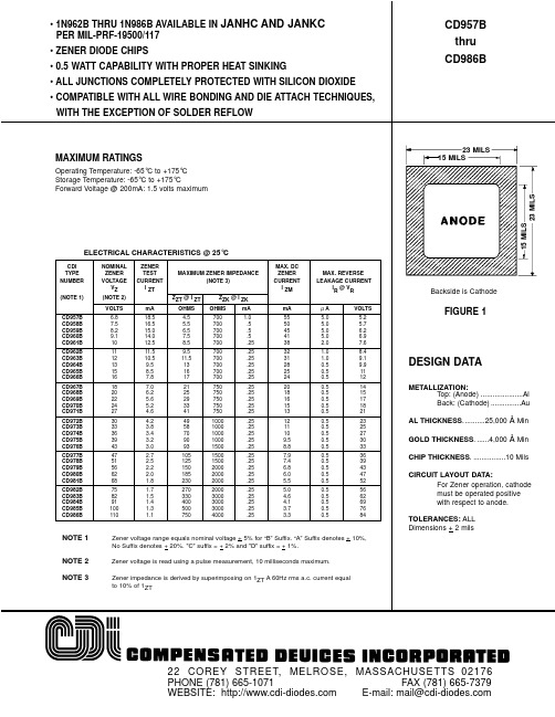
NOTE 1 NOTE 2 NOTE 3
Zener voltage range equals nominal voltage + 5% for “B” Suffix. “A” Suffix denotes + 10%, No Suffix denotes + 20%. "C" suffix = + 2% and "D" suffix = + 1%. Zener voltage is read using a pulse measurement, 10 milliseconds maximum. Zener impedance is derived by superimposing on 1ZT A 60Hz rms a.c. current equal to 10% of 1ZT
23 MILS 15 MILS
ELECTRICAL CHARACTERISTICS @ 25°C
CDI TYPE NUMBER (NOTE 1) NOMINAL ZENER VOLTAGE VZ (NOTE 2) VOLTS CD957B CD958B CD959B CD960B CD961B CD962B CD963B CD964B CD965B CD966B CD967B CD968B CD969B CD970B CD971B CD972B CD973B CD974B CD975B CD976B CD977B CD978B CD979B CD980B CD981B CD982B CD983B CD984B CD985B CD986B 6.8 7.5 8.2 9.1 10 11 12 13 15 16 18 20 22 24 27 30 33 36 39 43 47 51 56 62 68 75 82 91 100 110 mA 18.5 16.5 15.0 14.0 12.5 11.5 10.5 9.5 8.5 7.8 7.0 6.2 5.6 5.2 4.6 4.2 3.8 3.4 3.2 3.0 2.7 2.5 2.2 2.0 1.8 1.7 1.5 1.4 1.3 1.1 ZENER TEST CURRENT l ZT MAXIMUM ZENER IMPEDANCE (NOTE 3) ZZT @ l ZT OHMS 4.5 5.5 6.5 7.5 8.5 9.5 11.5 13 16 17 21 25 29 33 41 49 58 70 90 93 105 125 150 185 230 270 330 400 500 750 ZZK @ l ZK OHMS 700 700 700 700 700 700 700 700 700 700 750 750 750 750 750 1000 1000 1000 1000 1500 1500 1500 2000 2000 2000 2000 3000 3000 3000 4000 mA 1.0 .5 .5 .5 .25 .25 .25 .25 .25 .25 .25 .25 .25 .25 .25 .25 .25 .25 .25 .25 .25 .25 .25 .25 .25 .25 .25 .25 .25 .25 mA 55 50 45 41 38 32 31 28 25 24 20 18 16 15 13 12 11 10 9.5 8.8 7.9 7.4 6.8 6.0 5.5 5.0 4.6 4.1 3.7 3.3 MAX. DC ZENER CURRENT l ZM MAX. REVERSE LEAKAGE CURRENT lR @ VR
用户手册CD播放机中文版-NaimAudio

如果不可拆线插头电源与电源线断开(不管出于什么目的),必 须将此插头完全弃置不用。如果切断插头插入到电源插座,则存 在相当大的触电危险。
2.4 电源电路和导线
高保真音响系统通常与其他家用设备共用电源电路,其中部分设 备可能会导致电源波形失真。这种失真会反过来导致从电源变压 器发出机械嗡嗡声。部分Naim变压器体型大,因此其对这种失真 比较敏感,所以有必要在定位设备时考虑到变压器的嗡嗡声。
1.2 音箱导线
音箱导线的作用非常重要。导线至少应3.5米长,且每根长度相 等。建议一般情况下最大长度为20米,但部分Naim扩音器可能 采用更长的导线。
部分Naim扩音器只能与Naim扬声器导线共同使用,使用替代 品可能会降低扩音器性能,甚至破坏扩音器。虽然我们建议使用 Naim扬声器导线,但部分Naim扩音器可以与任何高品质的音箱 线共同使用。Naim扬声器导线具有方向性,应该使印刷的箭头指 向扬声器。随机提供的Naim扬声器连接器的设计符合欧洲安全 法,必须使用此连接器进行连接。
部分扬声器和支架拟用地板钉进行安装。定位及移动它们时应小 心,以避免人身伤害或损坏导线及设备表面。地面保护垫可以从 当地经销商或分销商获取以保护非地毯地板。
1
连接
2主电源3 Nhomakorabea一般安装
4
CD 555 简介和安装
5
CD 555 连接
6
CD 555 使用
7
CDX2 简介和安装
8
CDX2 连接
9
CDX2 使用
10 CD5 XS 简介和安装
11 CD5 XS 连接
12 CD5 XS 使用
13 CD5si 简介和安装
14 CD5si 连接
Transcribe中文使用说明

Transcribe中文使用说明Transcribe! 7.31.0 中文使用说明转录!帮助内容在窗户7.31版本版权?1998-2006七弦软件。
版权所有。
微软视窗媒体技术利用部分。
版权?1999 - 2002年的微软公司。
版权所有。
概述转录的!应用程序是一个助理的人有时候想找出一段音乐从记录,以写出来或者玩它自己。
通常的方法做这是使用CD或者反复听随身听生意各个位,用你的耳朵,你的大脑弄清正在发生的事情。
除非你是个乐感很强的人,那么你也需要一钢琴、吉他便于检查那个音符是哪个。
转录!不从根本上改变程序,但旨在提供的帮助使它更加方便、快捷的服务。
音乐是表现为滚动波形显示,你可以把标志物部分,措施和节拍和给那些条幅的名字,让你一直都知道你是怎么想的。
界面灵活播放和响应,比如你可以改变环路分,播放速度、沥青等而回放仍在继续。
“导航栏”给作品的全面了解和标记你下。
你可以点击它跳转到任何就说到了点子上。
多环能得救,并且召回。
有许多命令与选择和播放、和你可以控制它们从完全可配置的键盘的捷径。
你可以用各种各样的踏板控制回放如果你愿意的话,让各种操作——开始和停止播放,你的脚。
您可以设定“全球快捷方式——那就是,键盘快捷键,即使转录工作!不是积极的应用。
所以你可以用音乐记谱法包来写你的转录,同时还能够控制转录!只用来播放使用键盘(或者说确实踏板,如果你有任何的)。
其他特点:谱分析的特点能帮助识别安装、卸载、系统的要求系统要求彩色显示屏,至少一项决议,800 * 600视窗2000 / NT / XP,声卡。
转录!第7版也可用来苹果操作系统10.3.4或之后,Linux系统/ GTK。
如果你有一个更老的窗口(95 / 98 /我还是Mac(OS 7.5 - 10.2),你仍然可以经营转录!版本6这仍然可只要有需求。
参观七串网站的更多信息。
安装转录!如果你正在读这篇文章,你可能会已经安装它。
但对于完整性:转录!对于Windows分布作为一个self-installing执行(建造的Inno指导)很精彩。
1 国际标准Cd(中文 Part 1 2015.9.15)
火焰原子吸收光谱法
警告:本国际标准包括有危险的材料、操作和装置,本标准的使用者在使用前有责任制定健康安全的规程,并确保规范地应用。
1
本国际标准规定了硫化铜精矿、铅精矿、锌精矿中镉量的火焰原子吸收光谱测定方法,测定范围如下:
a)对于铜精矿,本方法适用的镉含量测定范围为0.01%0.30 %;
3
试样用盐酸、硝酸、氢氟酸和高氯酸溶解。在稀盐酸介质中使用空气-乙炔火焰,于原子吸收光谱仪波长228.8 nm处,用氘灯扣背景,测量镉的吸光度。按工作曲线法计算镉的含量。
4
分析过程中,所用试剂均为分析纯,所用的水为蒸馏水或相同纯度的水。
4.1盐酸(ρ201.19g/mL)。
4.2盐酸(1+1):
边搅拌边缓慢加500 mL盐酸(4.1)至500 mL水中。
狭缝宽度:0.2 nm
6
6.1
按ISO 12743要求制备试样。
6.2
采用多点多次取样的方式从试样中分取试料,称取0.50 g左右有代表性的试料,精确至0.1 mg。同时,按ISO 9599称取试料测定吸湿水份。
也可以参照附录A规定的方法直接从实验室样品中制备预干燥试样。
7
7.1
在重复性试验条件下,每个试样至少重复测定两次。
ISO 648,实验室玻璃器皿—单刻度移液管
ISO 1042,实验室玻璃器皿—单刻度容量瓶
ISO3696,实验室分析用水—规则及试验方法
ISO 4787,实验室玻璃器皿—容量器皿—测试容量和使用方法
ISO 9599,硫化铜、铅、锌精矿—试样中水分测定—重量法
ISO GUIDE 35,标准样品的鉴定—总则和统计原理
8
集成电路中文名称大全

集成电路中文名称大全型号规格性能说明型号规格性能说明SN74LSOO 四2输入与非门SN74LSO1 四2输入与非门SN74LSO2 四2输入与非门SN74LS03 四2输入与非门SN74LS04 六反相器SN74LS05 六反相器SN74LS06 六反相缓冲器/驱动器SN74LS07 六缓冲器/驱动器SN74LS08 四2输入与非门SN74LS09 四2输入与非门SN74LS10 三3输入与非门SN74LS11 三3输入与非门SN74LS12 三3输入与非门SN74LS13 三3输入与非门SN74LS14 六反相器.斯密特触发SN74LS15 三3输入与非门SN74LS16 六反相缓冲器/驱动器SN74LS17 六反相缓冲器/驱动器SN74LS20 双4输入与门SN74LS21 双4输入与门SN74LS22 双4输入与门SN74LS25 双4输入与门SN74LS26 四2输入与非门SN74LS27 三3输入与非门SN74LS28 四输入端或非缓冲器SN74LS30 八输入端与非门SN74LS32 四2输入或门SN74LS33 四2输入或门SN74LS37 四输入端与非缓冲器SN74LS38 双2输入与非缓冲器SN74LS40 四输入端与非缓冲器SN74LS42 BCD-十进制译码器SN74LS47 BCD-七段译码驱动器SN74LS48 BCD-七段译码驱动器SN74LS49 BCD-七段译码驱动器SN74LS51 三3输入双与或非门SN74LS54 四输入与或非门SN74LS55 四4输入与或非门SN74LS63 六电流读出接口门SN74LS73 双J-K触发器SN74LS74 双D触发器SN74LS75 4位双稳锁存器SN74LS76 双J-K触发器SN74LS78 双J-K触发器SN74LS83 双J-K触发器SN74LS85 4位幅度比较器SN74LS86 四2输入异或门SN74LS88 4位全加器SN74LS90 4位十进制波动计数器SN74LS91 8位移位寄存器SN74LS92 12分频计数器SN74LS93 二进制计数器SN74LS96 5位移位寄存器SN74LS95 4位并入并出寄存器SN74LS109 正沿触发双J-K触发器SN74LS107 双J-K触发器SN74LS113 双J-K负沿触发器SN74LS112 双J-K负沿触发器SN74LS121 单稳态多谐振荡器SN74LS114 双J-K负沿触发器SN74LS123 双稳态多谐振荡器SN74LS122 单稳态多谐振荡器SN74LS125 三态缓冲器SN74LS124 双压控振荡器SN74LS131 3-8线译码器SN74LS126 四3态总线缓冲器SN74LS133 13输入与非门SN74LS132 二输入与非触发器SN74LS137 地址锁存3-8线译码器SN74LS136 四异或门SN74LS139 双2-4线译码-转换器SN74LS138 3-8线译码/转换器SN74LS147 10-4线优先编码器SN74LS145 BCD十进制译码/驱动器SN74LS153 双4选1数据选择器SN74LS148 8-3线优先编码器SN74LS155 双2-4线多路分配器SN74LS151 8选1数据选择器SN74LS157 四2选1数据选择器SN74LS154 4-16线多路分配器SN74LS160 同步BDC十进制计数器SN74LS156 双2-4线多路分配器SN74LS162 同步BDC十进制计数器SN74LS158 四2选1数据选择器SN74LS164 8位串入并出移位寄存SN74LS161 4位二进制计数器SN74LS166 8位移位寄存器SN74LS163 4位二进制计数器SN74LS169 4位可逆同步计数器SN74LS165 8位移位寄存器SN74LS172 16位多通道寄存器堆SN74LS168 4位可逆同步计数器SN74LS174 6D型触发器SN74LS170 4x4位寄存器堆SN74LS176 可预置十进制计数器SN74LS173 4D型寄存器SN74LS182 超前进位发生器SN74LS175 4D烯触发器SN74LS189 64位随机存储器SN74LS181 运算器/函数发生器SN74LS191 二进制同步可逆计数器SN74LS183 双进位保存全价器SN74LS193 二进制可逆计数器SN74LS190 同步BCD十进制计数器SN74LS195 并行存取移位寄存器SN74LS192 BCD-同步可逆计数器SN74LS197 可预置二进制计数器SN74LS194 双向通用移位寄存器SN74LS238 3-8线译码/多路转换器SN74LS196 可预置十进制计数器SN74LS241 八缓冲/驱动/接收器SN74LS221 双单稳态多谐振荡器SN74LS243 四总线收发器SN74LS240 八缓冲/驱动/接收器SN74LS245 八总线收发器SN74LS242 四总线收发器SN74LS248 BCD-七段译码驱动器SN74LS244 八缓冲/驱动/接收器SN74LS251 三态8-1数据选择器SN74LS247 BCD-七段译码驱动器SN74LS256 双四位选址锁存器SN74LS249 BCD-七段译码驱动SN74LS258 四2选1数据选择器SN74LS253 双三态4-1数据选择器SN74LS260 双5输入或非门SN74LS257 四3态2-1数据选择器SN74LS266 四2输入异或非门SN74LS259 8位可寻址锁存器SN74LS275 七位树型乘法器SN74LS261 2x4位二进制乘发器SN74LS279 四R-S触发器SN74LS273 八进制D型触发器SN74LS283 4位二进制全加器SN74LS276 四J-K触发器SN74LS293 4位二进制计数器SN74LS280 9位奇偶数发生校检器SN74LS365 六缓冲器带公用启动器SN74LS290 十进制计数器SN74LS367 六总线三态输出缓冲器SN74LS295 4位双向通用移位寄存器SN74LS373 8D锁存器SN74LS366 六缓冲器带公用启动器SN74LS375 4位双稳锁存器SN74LS368 六总线三态输出反相器SN74LS386 四2输入异或门SN74LS374 8D触发器SN74LS393 双4位二进制计数器SN74LS377 8位单输出D型触发器SN74LS574 8位D型触发器SN74LS390 双十进制计数器SN74LS684 8位数字比较器SN74LS573 8位三态输出D型锁存器SN74HC11 三3输入与门SN74LS670 8位数字比较器SN7404 六反相器SN74HC00 四2输入与非门SN7406 六反相缓冲器/驱动器SN74HC02 四2输入或非门SN7407 六缓冲器/驱动器SN74HC03 四2输入或非门SN7414 六缓冲器/驱动器SN74HC04 六反相器SN7416 六反相缓冲器/驱动器SN74HC05 六反相器SN7440 六反相缓冲器/驱动器SN74HC08 四2输入与门SN7497 六反相缓冲器/驱动器SN74HC10 三3输入与非门74F00 高速四2输入与非门SN74HC14 六反相器/斯密特触发74F02 高速四2输入或非门SN74HC20 双四输入与门74F04 高速六反相器SN74HC21 双四输入与非门74F08 高速四2输入与门SN74HC27 三3输入与非门74F10 高速三3输入与门SN74HC30 八输入端与非门74F14 高速六反相斯密特触发SN74HC32 四2输入或门74F32 高速四2输入或门SN74HC42 BCD十进制译码器74F38 高速四2输入或门SN74HC73 双J-K触的器74F74 高速双D型触发器SN74HC74 双D型触发器74F86 高速四2输入异或门SN74HC76 双J-K触的器74F139 高速双2-4线译码/驱动器SN74HC86 四2输入异或门74F151 高速双2-4线译码/驱动器SN74HC107 双J-K触发器74F153 高速双4选1数据选择器SN74HC113 双J-K负沿触发器74F157 高速双4选1数据选择器SN74HC123 双稳态多谐振荡器74F161 高速6D型触发器SN74HC125 三态缓冲器74F174 高速6D型触发器SN74HC126 四三态总线缓冲器74F175 高速4D型触发器SN74HC132 二输入与非缓冲器74F244 高速八总线3态缓冲器SN74HC137 二输入与非缓冲器74F245 高速八总线收发器SN74HC138 3-8线译码/解调器74F373 高速8D锁存器SN74HC139 双2-4线译码/解调器SN74HCT04 六反相器SN74HC148 8选1数据选择器CD4001 4二输入或非门SN74HC151 双4选1数据选择器CD4002 双4输入或非门SN74HC154 4-16线多路分配器CD4006 18位静态移位寄存器SN74HC157 四2选1数据选择器CD4007 双互补对加反相器SN74HC161 4位二进制计数器CD4009 六缓冲器/转换-倒相SN74HC163 4位二进制计数器CD4010 六缓冲器/转换-正相SN74HC164 8位串入并出移位寄存器CD4011 四2输入与非门SN74HC165 8位移位寄存器CD4012 双4输入与非门SN74HC173 4D型触发器CD4013 置/复位双D型触发器SN74HC174 6D触发器CD4014 8位静态同步移位寄存SN74HC175 4D型触发器CD4015 双4位静态移位寄存器SN74HC191 二进制同步可逆计数器CD4016 四双向模拟数字开关SN74HC221 双单稳态多谐振荡器CD4017 10译码输出十进制计数器SN74HC238 3-8线译码器CD4018 可预置1/N计数器SN74HC240 八缓冲器CD4019 四与或选择门SN74HC244 八总线3态输出缓冲器CD4020 14位二进制计数器SN74HC245 八总线收发器CD4021 8位静态移位寄存器SN74HC251 三态8-1数据选择器CD4022 8译码输出8进制计数器SN74HC259 8位可寻址锁存器CD4023 三3输入与非门SN74HC266 四2输入异或非门CD4024 7位二进制脉冲计数器SN74HC273 8D型触发器CD4025 三3输入与非门SN74HC367 六缓冲器/总线驱动器CD4026 十进制/7段译码/驱动SN74HC368 六缓冲器/总线驱动器CD4027 置位/复位主从触发器SN74HC373 8D锁存器CD4028 BCD十进制译码器SN74HC374 8D触发器CD4029 4位可预置可逆计数器SN74HC393 双4位二进制计数器CD4030 四异或门SN74HC541 8位三态输出缓冲器CD4031 64位静态移位寄存器SN74HC573 8位三态输出D型锁存器CD4032 三串行加法器SN74HC574 8D型触发器CD4033 十进制计数器/7段显示SN74HC595 8位移位寄存器/锁存器CD4034 8位静态移位寄存器SN74HC4028 7级二进制串行加数器CD4035 4位并入/并出移位寄存器SN74HC4046 锁相环CD4038 3位串行加法器SN74HC4050 六同相缓冲器CD4040 12位二进制计数器SN74HC4051 8选1模拟开关CD4041 四原码/补码缓冲器SN74HC4053 三2选1模拟开关CD4042 四时钟D型锁存器SN74HC4060 14位计数/分频/振荡器CD4043 四或非R/S锁存器SN74HC4066 四双相模拟开关CD4044 四与非R/S锁存器SN74HC4078 3输入端三或门CD4046 锁相环SN74HC4511 7段锁存/译码驱动器CD4047 单非稳态多谐振荡器SN74HC4520 双二进制加法计数器CD4048 可扩充八输入门CD4502 可选通六反相缓冲器CD4049 六反相缓冲/转换器CD4503 六同相缓冲器CD4050 六正相缓冲/转换器CD4504 六电平转换器CD4051 单8通道多路转换/分配CD4508 双4位锁存器CD4052 双4通道多路转换/分配CD4510 BCD可预置可逆计数器CD4053 三2通道多路转换/分配CD4511 BCD7段锁存/译码/驱动CD4056 7段液晶显示译码/驱动CD4512 8通道数据选择器CD4060 二进制计数/分频/振荡CD4513 BCD7段锁存/译码/驱动CD4063 四位数值比较器CD4514 4-16线译码器CD4066 四双相模拟开管CD4515 4-16线译码器CD4067 16选1模拟开关CD4518 双BCD加法计数器CD4068 8输入端与非/与门CD4520 双二进制加法计数器CD4069 六反相器CD4521 24位分频器CD4070 四异或门CD4522 可预置BCD1/N计数CD4071 四2输入或门CD4526 可预置二进制1/N计数CD4072 双四输入或门CD4527 BCD系数乘发器CD4073 三3输入与门CD4528 双单稳态触发器CD4075 三3输入与门CD4531 12位奇偶校验电路CD4076 4位D型寄存器CD4532 8位优先编码器CD4077 四异或非门CD4538 双精密单稳态触发器CD4078 八输入或/或非门CD4539 双四路输据选择器CD4081 四输入与门CD4541 可编程振荡/计时器CD4082 双4输入与门CD4543 7段锁存/译码/驱动CD4085 双2组2输入与或非门CD4553 3位BCD计数器CD4086 可扩展2输入与或非门CD4555 双4选1译码器CD4093 四与非斯密特触发器CD4556 双4选1译码器CD4094 8位移位/贮存总线寄存CD4557 1-64位可变长度寄存器CD4096 3输入J-K触发器CD4558 BCD-7段译码器CD4098 双单稳态触发器CD4560 BCD码加法器CD4099 8位可寻址锁存器CD4561 BCD转换成9的补码输出CD40103 同步可预置减法器CD4566 工业定时基准发生器CD40106 六斯密特触发器CD4569 双4位可编程1/NBCDCD40107 双2输入与非缓冲/驱动CD4583 双斯密特触发器CD40110 计数/译码/锁存/驱动CD4584 4斯密特触发器CD40174 6D触发器CD4585 4位数值比较器CD40175 4D触发器CD4599 8位总线相容寻址锁存器CD40192 BCD可预置可逆计数器MC145106 频率合成器CD40193 二进制可预置可逆计数器MC145026 遥控编码器CD40194 4位双相移位寄存器MC145027 译码器4N25 晶体管输出LM24J 四运放(军用级)4N25MC 晶体管输出LM148J 通用四运放4N26 晶体管输出LM1875T 无线电控制/接收器4N27 晶体管输出LM224J 四运放(工业级)4N28 晶体管输出258N 分离式双电源双运放4N29 达林顿输出LM2901N 四电压比较器4N30 达林顿输出LM2904N 四运放4N31 达林顿输出LM301AN 通用运算放大器4N32 达林顿输出LM308N 单比较器4N33 达林顿输出LM311P 单比较器4N33MC 达林顿输出LM317L 可调三端稳压器/100mA4N35 达林顿输出LM317T 可调三端稳压器/1.5A4N36 晶体管输出LM317K 可调三端稳压器/3A4N37 晶体管输出LM318 高速宽带运放4N38 晶体管输出LM324K 通用四运放4N39 可控硅输出LM331N V-F/F-V转换器6N135 高速光耦晶体管输出LM336-2.5V 基准电压电路6N136 高速光耦晶体管输出LM336 5V 基准电压电路6N137 高速光耦晶体管输出LM337T 基准电压电路1A6N138 达林顿输出LM338K 可调三端稳压器5A6N139 达林顿输出LM339N 四比较器MOC3020 可控硅驱动输出LM348N 四741运放MOC3021 可控硅驱动输出LM358N 低功耗双运放MOC3023 可控硅驱动输出LM361N 高速差动比较器MOC3030 可控硅驱动输出LM386N 声频功率放大器MOC3040 过零触发可控硅输出LM3914N 十段点线显示驱动MOC3041 过零触发可控硅输出LM393N 低功耗低失调双比较器MOC3061 过零触发可控硅输出LM399H 精密基准源(6.9) MOC3081 过零触发可控硅输出LM723CN 可调正式负稳压器TLP521-1 单光耦LM733CN 视频放大器TLP521-2 双光耦LM741J 单运放TLP521-4 四光耦LM741CN 双运放TLP621 四光耦OP07 低噪声运放TIL113 达林顿输出OP27 超低噪声精密运放TIL117 TLL逻辑输出OP37 超低噪声精密运放PC814 单光耦TL062 低功耗JEFT输入双运放PC817 单光耦TL072 低噪声JEFTH11A2 晶体管输出ULN2003 周边七段驱动陈列H11D1 高压晶体管输出ULN2004 周边七段驱动陈列H11G2 电阻达林顿输出ULN2803 周边八段驱动陈列LF347N 宽带JFET输入四运放ULN2804 周边八段驱动陈列LF351N 宽带JFET输入运放ICL7106 3位ADC/驱动LCDLF353N JFET输入宽带运放ICL7107 3位半ADC/驱动LEDLF355N JFET输入运放ICL7109 4位半ADC/驱动LEDLF357N JFET宽带非全裣运放ICL7129 4位半ADC/LCD驱动LF398N 采样/保持电路ICL7135 ADC/LCD驱动BCD输出LF412N 低偏差飘移输入运放ICL7136 3位半CMOSADC/LCD驱动MC1377 彩色电视编码器ICL7218 CMOS低功耗运算放大器MC1403 精密电压基准源(2.5) ICL7650 整零运放斩波MC1413 周边七段驱动阵列ICL7652 整零运放斩波MC1416 周边七段驱动陈列ICL7660 CMOS直流-直流转换器MC14409 二进制脉冲拨号器ICL8038 函数信号发生器MC14433 3位半A/D转换器ICL8049 反对数放大器MC14489 多字符LED显示驱动器CA3140 单BIMOS运行MC145026 编码器CA3240 单BIMOS运行VD5026 编码器UC3842 WM电流型控制器MC145027 译码器UC3845 PWM电流型控制器VD5027 译码器DS12887 非易失实时时钟芯片MC145028 译码器L3845 中继接口电路MC145030 编码译码器SG3524 PWM解调调制器MC145106 频率合成器SG3525 PWM解调调制器MC145146 4位数据总线20106 前置放大器NE521 高速双差分比较器TCM5087 双音调发生器NE5532 双运放MM5832 实时钟电路NE5534 双运放TC14433 3位半A/D转换器NE555N 单运放TC232 并行/串行接口电路NE555J 时基电路军品极TC7106 3位半ADC/LCD驱动NE556 双级型双时基电路TC7107 3位半ADC/LED驱动NE564 锁相环TC7116 3位半ADC/LCD驱动带保NE565 锁相环TC7129 4位半ADC/LCDNE567 音调译码器TC7135 4位半ADC/LCD,BCD输出NE592 视频放大器TC7650 整零运放斩波MT8814 8x12模拟交换矩阵75107 四差分线驱动器MT8816 8x模拟交换矩阵75174 四差分线驱动器MT8870 综合DTMF接收器75175 三态四差分接收器MT8870 综合DTMF接收器75176 差分总线接收器MT8880 综合DTMF发生接收器75188 四线驱动器24LC01 128x8串行EEPROM 75189 四线驱动器24LC02 256x8串行EEPROM 75451 双外围驱动器24LC04 512x8串行EEPROM 75452 双外围驱动器93LC46 64x16串行EEPROM PAL16L8 FLASH200门93LC56 256x16串行EEPROM PALCE16V8-25 FLASH200门93LC66 512x8 256x16 EEPROM PALCE16V8-25JC FLASH200门(贴片)PIC16C52 384x12 单片机ATF16V8-25PC FLASH200门PIC16C54 512x12 单片机GAL16V8-25LP FLASH200门PCI16C56 512x12 单片机GAL16V8-25LPI 工业级FLASH200门PIC16C57 2048x12 单片机GALV8-20LD 军品级FLASH200门AT24C01 128x8串行EEPROM GAL16V8-15LP 军品级FLASH200门AT24C02 256x8串行EEPROM GAL16V8-15LPI 工业级FLASH200门AT24C04 512x8串行EEPROM PALCF20V8-25PC FLASH300门AT24C16 2Kx8串行EEPROM A TF20V8-25PC FLASH300门AT93C46 64x16串行EEPROM GAL20V8-25LP FLASH300门AT93C56 256x16串行EEPROM GAL20V8-25LPI 工业级FLASH门ATF16V8 FLASH200门GAL20V8-20LD 军品级门ATF20V8 FLASH300门高速GAL20V8-15LP 军品级门ATF22V10 FLASH500门高速低电流GAL20V8-15LPI 工业级FLASH门AT28C16 2Kx8CMOS并行EEPROM ATF22C10-25PC FLASH500门高速低电流AT28C17 2Kx8CMOS并行EEPROM ATF22C10-25PC FLASH500门高速低电流AT28C64 8Kx8并行EEPROM GAI22V10-25LP FLASH500门高速低电流AT28C256 32Kx8并行EEPROM PALCE22V10-15JC FLASH500门高速低电流AT28F010 128Kx8并行EEPROM 2716 8Kx8 NMOS EPROMA29C040 512Kx8 FLASH EEPROM 27C16 2Kx8 NMOS EPROMHM6116 2Kx8 CMOS 静态PAM 2732 4Kx8 NMOS EPROMHY6264 8Kx8 CMOS 静态RAM 27C32 4Kx8 NMOS EPROMHM6264 8Kx8 CMOS 静态RAM 2764F 8Kx8 NMOS EPROMIS62C64 8Kx8 高速CMOS 静态RAM 27C64F 8Kx8 NMOS EPROMHY62256 32Kx8 CMOS 静态RAM 2764ST 8Kx8 NMOS EPROMHM62256 32Kx8 CMOS 静态RAM 27C64ST 8Kx8 NMOS EPROMHM628128 128Kx8 CMOS 静态RAM 27C64NS 8Kx8 NMOS EPROMHM628256 256Kx8 CMOS 静态RAM 27128 16Kx8 NMOS EPROMHM628512 512Kx8 CMOS 静态RAM 27C128 16Kx8 NMOS EPROMHM628512 512Kx8 CMOS 静态RAM 27256 32Kx8 NMOS EPROMZ80 CP CTC PIO S10 27C256 32Kx8 NMOS EPROMLD8031AH 8位微处理器工业级MD27C256 16Kx8 CMOS EPROM8031 8位微处理器27HC256-45 16Kx8 高速CMOS EPROM80C31 8位CMOST微处理器27512 64Kx8 NMOS EPROM80C31NT 8位CMOST微处理器27C512 64Kx8 NMOS EPROMN80C31BH 8位CMOST微处理器贴片MD27C512 64Kx8 NMOS EPROMLD80C31BH 8位CMOST微处理器27HC512-45 64Kx 高速CMOS EPROM MD80C31BH 8位CMOST微处理器27C010 128Kx8 CMOS EPROM8032 8位微处理器27HC010-30 128Kx8 CMOS EPROMLD8032AH 8位CMOST微处理器27C020 256Kx8 CMOS EPROM80C32 8位CMOS微控制器27C040 512Kx8 CMOS EPROM8039 8位微控制器27HC040-30 512Kx8 CMOS EPROM80C39 8位微控制器27C080 1024Kx8 CMOS EPROM8051 8位微控制器2816 2Kx8 并行EEPROM80C51 8位CMOS微控制器28C16 2Kx8 CMOS 并行EEPROM80C552 8位微控制器2817 2Kx8 并行EEPROM80C552新8位微控制器28C17 2Kx8 CMOS 并行EEPROM8080 8位微处理器2864 8Kx8 并行EEPROM8085 8位NMOS微处理器28C64 8Kx8 CMOS 并行EEPROM80C85 8位NMOS微处理器28C64B15JC 8Kx8 CMOS 并行EEPROM 8086 16位NMOS微处理器28C256 32Kx8 CMOS 并行EEPROM80C86 CMOS 16位微处理器28F010 128Kx 高速并行EEPROM8087 数值协处理器2810 128Kx 高速并行EEPROM8088 8位HMOS微处理器28F020 256Kx 高速并行EEPROM80C88 CMOS 8位HMOS微处理器28F020-150 256Kx 高速并行EEPROM 8097 16位单片机28F256 32Kx 高速并行EEPROM8098 准16位微控制器28F256 32Kx 高速并行EEPROM8155 通用接口电路29C010 128Kx8 FLASH EEPROM81C55 CMOS通用接口电路29C040 512Kx8 FLASH EEPROM8212 时钟发生器和驱动器29F040-90 512Kx8 FLASH EEPROM8228 系统控制和总线驱动器AD1674KN 12位2KHZ带采保ADC8237 DMA控制器AD202JY 小型2KHZ隔离放大器82C37 CMOS DMA 控制器AD232JN 线路驱动接收器8243 扩展器AD521JD 电阻设置精密仪放器82C43 CMOS I/O扩展器AD574AJD 12位数模转换器8250 异步通信接口电路AD590JH 宽温度范围传感器82C50 CMOS 异步通信接口电路AD624AD 精密仪表放大器8251 串行通信接口电路AD650JN 低线性误差压频转换器MD8251A 异步通信接口电路ADC0804 8位A/D转换器82C51 CMOS 异步通信接口电路ADC0808 8位A/D转换器8253 可编程区间计数器ADC0809 8位A/D转换器82C53 CMOS 可编程区间计数器ADC0820 8位A/D转换器8254 可编程间隔定时器DAC0808 8位A/D转换器83C54 CMOS 可编程间隔定时器DAC0832 8位A/D转换器LP82C54 CMOS 可编程间隔定时器DAC1210 12位A/D转换器8255 可编程外围并行接口电路MAX1487CPA ESD保护RS-485MD8255A 可编程外围并行接口电路MAX1202CPE RS-232接口电路82C55 CMOS 可编程外围并行接口MAX232CPA RS-232接口电路8257 可编程DMA控制器MAX485CPA RS-485接口电路8259 可编程中段控制器MAX488CPA RS-485接口电路82C59 CMOS 可编程中段控制器MAX706CPA UP监控电路8279 可编程键盘显示器接口电路MAX7219CNA 8位显示驱动器82C79 CMOS 8279 MAX756CPA UP监控电路8282 8位锁存器MAX483 UP监控电路8283 8位锁存器TDA1521 低电平检测宽带放大器8284 时钟发生器和驱动器TDA2003A 单功率放大器5-10W 8286 8位总线收发器TDA2030A 单功率放大器>10W8287 8位总线收发器TDA2822 桑苗双功率放大器8288 总线控制器87C552 8位微控制器82C88 CMOS 总线控制器89C1051PC 1K8位FLASH单片机8748 8位微控制器89C2051PC 2K8位FLASH单片机8749 8位微控制器89C2051PI 2K8位FLASH单片机8751 8位微控制器89C51PC 4K8位FLASH单片机87C51 CMOS 8位控制器89C51PI 4K8位FLASH单片机87C51FA CMOS 8位微控制器89C52PC 2K8位FLASH单片机87C52 87C51加强型89C52PI 2K8位FLASH单片机89C55PC 20Kx8位89C52JC 2K8位FLASH单片机。
TA2020-020中文资料

RL= 8Ω
RL= 4Ω
Output Power (W)
1 of 13
TA2020-020, Rev. 4.0, 09.00
元器件交易网
TECHNICAL INFORMATION
Absolute Maximum Ratings (Note 1)
SYMBOL VDD TSTORE TA TJ Supply Voltage Storage Temperature Range Operating Free-air Temperature Range Junction Temperature PARAMETER
TA2020-020, Rev. 4.0, 09.00
3 of 13
元器件交易网
TECHNICAL INFORMATION
Pin Description
Pin 2, 8 3, 7, 16 4 6 9, 12 10, 13 11 14 17 18 19, 28 20 21, 23, 26, 24 22, 25 1, 5, 15 27 29 30 31, 32 Function V5D, V5A AGND1, AGND2, AGND3 REF OVERLOADB VP1, VP2 IN1, IN2 MUTE BIASCAP SLEEP FAULT PGND2, PGND1 DGND OUTP2 & OUTM2; OUTP1 & OUTM1 VDD2, VDD1 NC VDDA CPUMP 5VGEN DCAP2, DCAP1 Description Digital 5VDC, Analog 5VDC Analog Ground
A-Weighted, input AC grounded
100
Notes: 1) Minimum and maximum limits are guaranteed but may not be 100% tested. 2) For operation in ambient temperatures greater than 25°C, the device must be derated based on the maximum junction temperature and the thermal resistance determined by the mounting technique.
CD74HC221M中文资料

• Q and Q Buffered Outputs
• Separate Resets
• Wide Range of Output-Pulse Widths
• Schmitt Trigger on B Inputs
For VO > -0.5V or VO < VCC + 0.5V . . . . . . . . . . . . . . . . . . . .±25mA DC VCC or Ground Current, ICC . . . . . . . . . . . . . . . . . . . . . . . . .±50mA
Copyright © Harris Corporation 1997
1
File Number 1670.1
元器件交易网 Functional Diagram
CD74HC221, CD74HCT221
1CX 1RX
14
15
VCC
1CX
1CXRX
13
1A
1Q
1
MONO 1
N/A
Maximum Junction Temperature (Plastic Package) . . . . . . . . 150oC
Maximum Storage Temperature Range . . . . . . . . . .-65oC to 150oC
Maximum Lead Temperature (Soldering 10s) . . . . . . . . . . . . . 300oC
[ /Title (CD74 HC221 , CD74 HCT22 1) /Subject (High Speed CMOS Logic Dual Monos table Multi-
CY7C1515AV18资料

Page 2 of 31 [+] Feedback
元器件交易网
Logic Block Diagram (CY7C1513AV18)
CY7C1511AV18, CY7C1526AV18 CY7C1513AV18, CY7C1515AV18
18 D[17:0]
A(19:0) 20
■ Variable drive HSTL output buffers
■ JTAG 1149.1 compatible test access port
■ Delay Lock Loop (DLL) for accurate data placement
Configurations
CY7C1511AV18 – 8M x 8 CY7C1526AV18 – 8M x 9 CY7C1513AV18 – 4M x 18 CY7C1515AV18 – 2M x 36
Address Register
21
A(20:0)
2M x 8 Array 2M x 8 Array 2M x 8 Array 2M x 8 Array
Read Data Reg. 32 16
16
Control Logic
RPS
C C
Reg.
Reg. 8 8
Reg.
8
8
8
CQ CQ Q[7:0]
Logic Block Diagram (CY7C1526AV18)
Address Register
21
A(20:0)
2M x 9 Array 2M x 9 Array 2M x 9 Array 2M x 9 Array
Read Data Reg. 36 18
WKO101MCPCD0KR;WKO151MCPCD0KR;WKO331MCPCD0KR;WKO471MCPCD0KR;WKO680MCPCD0KR;中文规格书,Datasheet资料

Ceramic AC CapacitorsClass X1, 440 V AC /Class Y2, 300 VAC For technical questions, contact slcap@Document Number: 2220448Revision: 31-Jan-06WKOVishay DraloricDESIGN:Disc capacitors with epoxy coatingRATED VOLTAGE U R :(X1):440 V AC , 50 Hz (IEC 60384-14.2)(Y2): 300 V AC , 50 Hz (IEC 60384-14.2)250 V AC , 60 Hz (UL1414, CSA C22.2)DIELECTRIC STRENGTH BETWEEN LEADS:Component test:2600 V AC , 50 Hz, 2 sAs repeated test admissible only once with 2340 V AC , 50 Hz, 2 sRandom sampling test (destructive test): 2600 V AC , 50 Hz, 60 sDIELECTRIC STRENGTH OF BODY INSULATION:2600 V AC , 50 Hz, 60 s (destructive test)DISSIPATION FACTOR tan δ:≤ 25 • 10-3INSULATION RESISTANCE Ris:≥ 6 • 109 ΩCATEGORY TEMPERATURE RANGE ϑA :(- 40 to + 125) °CCLIMATIC CATEGORY ACC. TO EN60068-1:40/125/21COATING:Epoxy, dipped, insulating, flame retarding acc. to UL 94V-0TAPING AND SPECIAL LEAD CONFIGURATIONS:On requestMARKING:WKO 33 pF to 1.0 nF WKO 1.5 nF to 4.7 nFAll approval marks are also shown on the label.440 300 250 ~• Dimensions in mmImped ance (Z) as a function of frequency (f) at Ta = 20 °C (average). Measurement with lead length50 mm.Document Number: 22204For technical questions, contact slcap@Revision: 31-Jan-0649WKOCeramic AC CapacitorsClass X1, 440 V AC /Class Y2, 300 VACVishay Draloric* Standard lead configuration, other lead spacing and diameter available on request.** Capacitance values from 1000 pF to 4700 pF: The alternative usage of smaller VKO series is recommended for new application.ORDERING INFORMATION, CERAMIC X1 / Y2 CAPACITORS WKOCAPACITANCE**(pF)TOL.(%) D x s (mm) F ± 1*(mm) d ± 0.05*(mm)V ± 0.5*(mm)ORDERING CODE CLASS 1N75033± 10 %, ± 20 %8.0 x 5.07.50.6 1.6WKO330 CP KR 478.0 x 5.0WKO470 CP KR CLASS 2K120068± 10 %, ± 20 %8.0 x 5.07.50.6 1.9WKO680 CP KR CLASS 2K1500100± 10 %, ± 20 %8.0 x 5.07.50.61.9WKO101 CP KR CLASS 2K2000150± 10 %, ± 20 %8.0 x 5.07.50.6 1.9WKO151 CP KR 2208.0 x 5.0WKO221 CP KR 3308.0 x 5.0WKO331 CP KR CLASS 2K4000470± 10 %, ± 20 %8.0 x 5.07.50.62.0WKO471 CP KR 6809.0 x 5.0WKO681 CP KR 100010.0 x 5.00.81.6WKO102 CP KR 150012.0 x 5.0WKO152 CP KR 220013.0 x 5.0WKO222 CP KR 330015.0 x 5.0WKO332 CP KR 390016.0 x 5.0WKO392 CP KR 470018.0 x 5.012.5WKO472 CP KRORDERING CODE7th digit Capacitance T olerance:± 10 % = K ± 20 % = M10th to 12th digit Lead Configuration (see General Information)R14th digitRoHS Compliant ComponentORDERING INFORMATIONWKO 392K CP CJ0K R SERIESCAP. VALUETOLERANCERATED VOLTAGELEADCONFIGURATIONINTERNAL CODERoHS COMPLIANTLegal Disclaimer NoticeVishayDisclaimerAll product specifications and data are subject to change without notice.Vishay Intertechnology, Inc., its affiliates, agents, and employees, and all persons acting on its or their behalf (collectively, “Vishay”), disclaim any and all liability for any errors, inaccuracies or incompleteness contained herein or in any other disclosure relating to any product.Vishay disclaims any and all liability arising out of the use or application of any product described herein or of any information provided herein to the maximum extent permitted by law. The product specifications do not expand or otherwise modify Vishay’s terms and conditions of purchase, including but not limited to the warranty expressed therein, which apply to these products.No license, express or implied, by estoppel or otherwise, to any intellectual property rights is granted by this document or by any conduct of Vishay.The products shown herein are not designed for use in medical, life-saving, or life-sustaining applications unless otherwise expressly indicated. Customers using or selling Vishay products not expressly indicated for use in such applications do so entirely at their own risk and agree to fully indemnify Vishay for any damages arising or resulting from such use or sale. Please contact authorized Vishay personnel to obtain written terms and conditions regarding products designed for such applications.Product names and markings noted herein may be trademarks of their respective owners.Document Number: Revision: 18-Jul-081分销商库存信息:VISHAY-BC-COMPONENTSWKO101MCPCD0KR WKO151MCPCD0KR WKO331MCPCD0KR WKO471MCPCD0KR WKO680MCPCD0KR WKO471MCPCJ0KR WKO101MCPSJBKR WKO101MCPSTAKR WKO221MCPSTAKR WKO331MCPSWGKR WKO471MCPRLASR WKO681MCPCD0KR WKO330MCPQC0KR WKO470MCPCD0KR WKO101MCPBRAKR WKO101MCPCF0KR WKO101MCPCRAKR WKO101MCPCRBKR WKO101MCPCREKR WKO101MCPQC0KR WKO101MCPUALKR WKO151MCPCF0KR WKO151MCPCRAKR WKO221MCPCD0KR WKO221MCPCF0KR WKO221MCPCFGKR WKO221MCPCRAKR WKO221MCPCRBKR WKO221MCPCREKR WKO221MCPTCRKR WKO221MCPUARKR WKO331MCPCF0KR WKO331MCPCRAKR WKO331MCPEF0KR WKO471MCPBLAKR WKO471MCPCF0KR WKO471MCPCFGKR WKO471MCPCRAKR WKO471MCPCRBKR WKO471MCPCREKR WKO471MCPDRUKR WKO471MCPERUKR WKO471MCPTCRKR WKO471MCPUALKR WKO680MCPCF0KR WKO101MCPSAHKR WKO101MCPSRWKR WKO221MCPSRWKR WKO221MCPSSLKR WKO331MCPSAVKR WKO471KCPCD0KR WKO681MCPCF0KR WKO681MCPCRAKR WKO681MCPCRBKR WKO681MCPCREKR WKO681MCPSAHKR WKO330MCPCD0KR WKO330MCPCF0KR WKO330MCPCRAKR WKO330MCPEF0KR WKO470MCPCF0KR WKO470MCPCRAKR WKO470MCPCREKR WKO471MCPDK0KR WKO330KCPBF0KR WKO330KCPQE0KR WKO101KCPCF0KR WKO101KCPCRAKR WKO101KCPCRBKR WKO151KCPCF0KR WKO221KCPCF0KR WKO221KCPCFGKR WKO221KCPCRAKR WKO331KCPCF0KR WKO471KCPCF0KR WKO471KCPCRAKR WKO471KCPCREKR WKO681KCPBF0KR WKO681KCPCF0KR WKO330KCPCF0KR WKO470KCPCF0KR WKO470KCPCRAKR WKO222MCPRMRKR WKO102MCPCH0KR WKO102MCPQC0KR WKO152MCPCD0KR WKO152MCPCH0KR WKO152MCPQE0KR WKO102MCPSTAKR WKO102MCPCF0KR WKO102MCPCFGKR WKO102MCPCJ0KR WKO102MCPCRAKR WKO102MCPCRBKR WKO102MCPCRCKR WKO102MCPCREKR WKO102MCPDF0KR WKO102MCPDJ0KR WKO102MCPQD0KR WKO152MCPCF0KR WKO152MCPCJ0KR WKO152MCPCJGKR WKO152MCPCRAKR WKO152MCPCREKR WKO152MCPQH0KR WKO102MCPSSLKR WKO222MCPCD0KR WKO222MCPCH0KR WKO222MCPNR0KR WKO222MCPQL0KR WKO222MCPYC0KR WKO102KCPCF0KR WKO102KCPCJ0KR WKO152KCPCJ0KR WKO222MCPCF0KR WKO222MCPCJ0KR WKO222MCPCJGKR WKO222MCPCRAKR WKO222MCPCRBKR WKO222MCPCREKR WKO222MCPCRUKR WKO222MCPCRYKR WKO222MCPDJ0KR。
Exact Audio Copy中文版

Exact Audio Copy中文版Exact Audio Copy 1.6是一款专业可靠的CD抓轨软件,完成创建音频时不仅拥有超快的翻录速度,还能够保留原始的高质量,不会造成任何的损失,帮助用户们轻松抓取捕捉任何CD 文件的音轨。
其采用强大且先进的DVD解码算法技术,可以帮助用户轻松完全解码CSS加密和区域码限制,非常方便。
该软件除了能够抓取任何CD的音轨外,还支持音频文件转换功能,它内置技术先进的采样率转换器,能够在所有格式之间转换音频文件,采用精准音频引擎,支持音乐CD格式转换成绝大多数多媒体文件格式,满足用户使用需求。
这里为大家伙带来的是Exact Audio Copy中文版,已由大神经过完美汉化,进入软件主界面为中文语言,特别适合那些不怎么懂英文的用户使用,摆脱了语言束缚,完全符合他们的使用需求,需要的朋友快来下载进行使用体验吧。
功能介绍1、提取技术在安全模式下,此程序将读取每个音频扇区至少两次,或依赖某些驱动器能够随音频数据返回的扩展错误信息。
这就是该程序比其他撕裂程序慢的原因之一。
但是通过使用该技术,可以检测到不相同的扇区。
如果发生错误(读取或同步错误),程序将继续读取该扇区,直到16次重试相同为止,但是最多读取1次,3次或5次(根据所选的错误恢复质量)这16次重试。
因此,在最坏的情况下,坏扇区最多可读取82次!但是这项工作将通过比较所有重试来帮助程序获得最佳结果。
如果不确定音频流是否正确(至少不能说大约99.5%),程序将告诉用户发生(可能)读取错误的位置。
该程序还尝试纠正出现在磁道第一块上的抖动伪像,以便每次提取都应该完全相同。
在具有“精确流”功能的驱动器上,这是可以保证的。
当然,这项技术要稍微复杂一点,尤其是对于某些实现了缓存的CD驱动器而言。
当驱动器缓存音频数据时,每个读取的扇区将从驱动器缓存中读取,并且始终保持相同。
基本上有几种清除缓存的方法。
在较新的版本中,它将覆盖扇区,因此高速缓存包含CD上其他位置的扇区。
急性缺血性脑卒中患者外周血白细胞CD11b、CD18表达变化研究
急性缺血性脑卒中患者外周血白细胞CD11b、CD18表达变化研究唐方;陈槐卿;徐朝义;张峻梅;高励;刘凯【期刊名称】《中国神经免疫学和神经病学杂志》【年(卷),期】2003(010)002【摘要】目的探讨急性脑卒中患者外周血白细胞黏附分子CD11b、CD18的表达,以及其在急性缺血性脑损伤发生、发展中的作用. 方法采用流式细胞术,用单克隆抗体标记定量测定32例急性脑卒中患者发作24 h内外周血白细胞CD11b、CD18的表达量,以平均荧光强度(MFI)的大小来表示CD11b、CD18的相对含量,在发病72 h、7 d后再分别测定1次.以40例健康者作对照. 结果发病24 h内患者组白细胞表面黏附分子CD11b、CD18的表达显著高于对照组(P<0.01);在发病72 h内患者组CD11b、CD18的表达逐渐降低,但仍高于对照组(P<0.05);发病7 d后,其结果与对照组相比差异无显著性(P>0.05). 结论急性脑卒中发病时,白细胞被激活,黏附分子CD11b、CD18表达上调,介导白细胞与内皮细胞黏附增强,可能会加重缺血后迟发性神经元死亡的病理生理过程.【总页数】4页(P119-122)【作者】唐方;陈槐卿;徐朝义;张峻梅;高励;刘凯【作者单位】成都市第三人民医院检验科,四川,成都,610031;华西医科大学生物医学工程研究室,四川,成都,610061;成都市第三人民医院神经内科,四川,成都,610031;成都市第三人民医院检验科,四川,成都,610031;成都市第三人民医院神经内科,四川,成都,610031;成都市第三人民医院检验科,四川,成都,610031【正文语种】中文【中图分类】R743.3【相关文献】1.CD11b、CD18、WBC、CRP测定在急性缺血性脑卒中诊断中的作用 [J], 黄杰;郭平;唐方;曾屏;李建红;孙蜀勇2.早期糖尿病肾病外周血多形核白细胞黏附分子CD11b/CD18表达变化 [J], 倪海祥;叶真;杨雪辉;魏佳平;黄琦;邵国民3.冠心病患者白细胞膜黏附分子CD11b/CD18表达的研究 [J], 王雄;刘胜辉;贾永平;窦岩;李运乾4.急性胆管炎时肝组织ICAM-1与循环PMN表面CD11b、CD18的表达变化 [J], 黄显凯;韩本立;朱锡光5.银屑病患者细胞CD11b、CD18及IL-8、IFN-γ变化的相关性研究 [J], 陈永生;张慧玲;孙庆凯因版权原因,仅展示原文概要,查看原文内容请购买。
人创伤性休克时白细胞表面LFA-1、Mac-1、CD18的表达
人创伤性休克时白细胞表面LFA-1、Mac-1、CD18的表达王妍春;赵克森【期刊名称】《微循环学杂志》【年(卷),期】1999(9)3【摘要】探讨人创伤性休克时白细胞表面LFA-1、Mac-1和CD18表达变化。
方法:间接免疫荧光标记法。
结果:创伤性休克后多形核粒细胞(PMNs)表面LFA-1、Mac-1和CD18表达呈下降趋势,但无显著意义(P>0.05)。
单核细胞表面LFA-1、Mac-1和CD18表达呈上升趋势,以CD18为显著(P<0.05)。
结论:创伤后PMNs表面粘附分子表达量与它对内皮的粘附存在不一致性,而单核细胞粘附也似乎不仅仅依赖于粘附分子的表面受体表达增强。
提示,单核细胞与PMNs在参与粘附反应时其表面CD18表达量变化不一致,其功能调节是否一致尚待查明。
【总页数】3页(P16-18)【关键词】创伤性休克;白细胞;粘附分子;整合蛋白【作者】王妍春;赵克森【作者单位】中国人民解放军广州军区广州总医院肾内科;中国人民解放军第一军医大学病理生理学教研室【正文语种】中文【中图分类】R605.971【相关文献】1.创伤性休克大鼠外周血白细胞表面LFA-1、ICAM-1表达的研究 [J], 王妍春;赵克森2.脑梗死急性期白细胞CD11a,CD18 和LFA-1表达与梗死体积的关系 [J], 马国胜;裴世澄;梁德胜;刘宁;杨金升3.细胞粘附分子LFA-1,MAC-1在大鼠急性坏死性胰腺炎合并多器官损伤模型中白细胞表面表达的动态研究及其意义 [J], 孙威;王强;王仲秋;渡边泰宏;土岐彰4.胶体金标记法测定创伤性休克时PMNs表面 LFA-1的表达 [J], 王妍春;赵克森5.创伤性休克病人粒细胞表面Mac-1、CD18的表达 [J], 王妍春;赵克森因版权原因,仅展示原文概要,查看原文内容请购买。
- 1、下载文档前请自行甄别文档内容的完整性,平台不提供额外的编辑、内容补充、找答案等附加服务。
- 2、"仅部分预览"的文档,不可在线预览部分如存在完整性等问题,可反馈申请退款(可完整预览的文档不适用该条件!)。
- 3、如文档侵犯您的权益,请联系客服反馈,我们会尽快为您处理(人工客服工作时间:9:00-18:30)。
Types CD17, CD18 & CDV18, High-Frequency, Mica CapacitorsHigh-Frequency Capacitors for CATV and RF ApplicationsTypes CD17 and CD18 assure controlled, reasonance-free performance through 1 GHz. Insertion loss data is typically flat within ±0.1 dB over the entire frequency range, and is specified to be flat within ±0.2 dB. Interchangeable with the most popular, common mica capacitors, Type CD17 is available in the same case sizes and lead spacing as CD15; CD18, in the same case sizes and lead spacing as CD19, and CDV18, in the same as CDV19.• Shockproof and delamination free• Near zero capacitance change with (t), (V) and (f)• Very high Q at UHF/VHF frequencies • 0.0005 typical dissipation factor• 100,000 V/µs dV/dt capability minimum • Low, notch-free impedance to beyond 1 GHz • Ultra low ESR for cool operationVoltage Range:100 Vdc to 1,000 Vdc Capacitance Range: 1 pF to 5,100 pF Capacitance Tolerance: ±1⁄2 pF (D), ±1 pF (C), ±1⁄2% (E), ±1% (F), ±2% (G), ±5% (J) Temperature Range:–55 °C to +150 °CTypical Perfomance CurvesSpecificationsHighlightsMeasured at point where phenolic cone becomes a cylinderS ±.031..078. Max.no solderH Max.1.Min.元器件交易网Types CD17, CD18 & CDV18, High-Frequency, Mica CapacitorsCap. Catalog Volt L H T S D Cap. Catalog Volt L H T S D (pF)Part Number Rate in (mm) in (mm) in (mm)in (mm) in (mm)(pF)Part Number Rate in (mm) in (mm) in (mm)in (mm) in (mm)1CD17CD010D03 500.450 (11.4) .360 ( 9.1) .170 (4.3) .234 (5.9) .025 (.6) 270CD17FD271J03 500.470 (11.9) .390 ( 9.9) .210 (5.3) .234 (5.9) .025 (.6) 2CD17CD020D03 500.450 (11.4) .360 ( 9.1) .170 (4.3) .234 (5.9) .025 (.6) 270CD18FD271J03 500.640 (16.3) .500 (12.7) .190 (4.8) .344 (8.7) .032 (.8) 3CD17CD030D03 500.450 (11.4) .360 ( 9.1) .170 (4.3) .234 (5.9) .025 (.6) 270CDV18FF271J03 1000.640 (16.3) .500 (12.7) .190 (4.8) .344 (8.7) .032 (.8) 4CD17CD040D03 500.450 (11.4) .360 ( 9.1) .170 (4.3) .234 (5.9) .025 (.6) 300CD17FD301J03 500.470 (11.9) .390 ( 9.9) .210 (5.3) .234 (5.9) .025 (.6) 5CD17CD050D03 500.450 (11.4) .360 ( 9.1) .170 (4.3) .234 (5.9) .025 (.6) 300CD18FD301J03 500.640 (16.3) .500 (12.7) .190 (4.8) .344 (8.7) .032 (.8) 6CD17CD060D03 500.450 (11.4) .360 ( 9.1) .170 (4.3) .234 (5.9) .025 (.6) 300CDV18FF301J03 1000.650 (16.5) .510 (13.0) .200 (5.1) .344 (8.7) .032 (.8) 7CD17CD070D03 500.450 (11.4) .360 ( 9.1) .170 (4.3) .234 (5.9) .025 (.6) 330CD17FD331J03 500.470 (11.9) .390 ( 9.9) .210 (5.3) .234 (5.9) .025 (.6) 8CD17CD080D03 500.450 (11.4) .360 ( 9.1) .170 (4.3) .234 (5.9) .025 (.6) 330CD18FD331J03 500.640 (16.3) .500 (12.7) .190 (4.8) .344 (8.7) .032 (.8) 9CD17CD090D03 500.450 (11.4) .360 ( 9.1) .170 (4.3) .234 (5.9) .025 (.6) 330CDV18FF331J03 1000.650 (16.5) .510 (13.0) .200 (5.1) .344 (8.7) .032 (.8) 10CD17CD100J03 500.450 (11.4) .360 ( 9.1) .170 (4.3) .234 (5.9) .025 (.6) 360CD17FD361J03 500.470 (11.9) .390 ( 9.9) .210 (5.3) .234 (5.9) .025 (.6) 12CD17CD120J03 500.450 (11.4) .360 ( 9.1) .170 (4.3) .234 (5.9) .025 (.6) 360CD18FD361J03 500.640 (16.3) .510 (13.0) .200 (5.1) .344 (8.7) .032 (.8) 15CD17CD150J03 500.450 (11.4) .360 ( 9.1) .170 (4.3) .234 (5.9) .025 (.6) 360CDV18FF361J03 1000.650 (16.5) .510 (13.0) .200 (5.1) .344 (8.7) .032 (.8) 18CD17CD180J03 500.450 (11.4) .360 ( 9.1) .170 (4.3) .234 (5.9) .025 (.6) 390CD17FD391J03 500.470 (11.9) .390 ( 9.9) .210 (5.3) .234 (5.9) .025 (.6) 20CD17ED200J03 500.450 (11.4) .360 ( 9.1) .170 (4.3) .234 (5.9) .025 (.6) 390CD18FD391J03 500.640 (16.3) .510 (13.0) .200 (5.1) .344 (8.7) .032 (.8) 22CD17ED220J03 500.450 (11.4) .360 ( 9.1) .170 (4.3) .234 (5.9) .025 (.6) 390CDV18FF391J03 1000.650 (16.5) .510 (13.0) .210 (5.3) .344 (8.7) .032 (.8) 24CD17ED240J03 500.450 (11.4) .360 ( 9.1) .170 (4.3) .234 (5.9) .025 (.6) 430CD17FD431J03 500.470 (11.9) .400 (10.2) .220 (5.6) .234 (5.9) .025 (.6) 27CD17ED270J03 500.450 (11.4) .360 ( 9.1) .170 (4.3) .234 (5.9) .025 (.6) 430CD18FD431J03 500.640 (16.3) .510 (13.0) .200 (5.1) .344 (8.7) .032 (.8) 27CDV18EF270J03 1000.640 (16.3) .500 (12.7) .190 (4.8) .344 (8.7) .032 (.8) 430CDV18FF431J03 1000.650 (16.5) .510 (13.0) .210 (5.3) .344 (8.7) .032 (.8) 30CD17ED300J03 500.450 (11.4) .360 ( 9.1) .170 (4.3) .234 (5.9) .025 (.6) 470CD17FD471J03 500.470 (11.9) .400 (10.2) .220 (5.6) .234 (5.9) .025 (.6) 30CDV18EF300J03 1000.640 (16.3) .500 (12.7) .190 (4.8) .344 (8.7) .032 (.8) 470CD18FD471J03 500.640 (16.3) .510 (13.0) .200 (5.1) .344 (8.7) .032 (.8) 33CD17ED330J03 500.450 (11.4) .360 ( 9.1) .170 (4.3) .234 (5.9) .025 (.6) 470CDV18FF471J03 1000.650 (16.5) .510 (13.0) .210 (5.3) .344 (8.7) .032 (.8) 33CDV18EF330J03 1000.640 (16.3) .500 (12.7) .190 (4.8) .344 (8.7) .032 (.8) 500CD17FD501J03 500.470 (11.9) .400 (10.2) .220 (5.6) .234 (5.9) .025 (.6) 36CD17ED360J03 500.450 (11.4) .360 ( 9.1) .170 (4.3) .234 (5.9) .025 (.6) 500CD18FD501J03 500.640 (16.3) .510 (13.0) .200 (5.1) .344 (8.7) .032 (.8) 36CDV18EF360J03 1000.640 (16.3) .500 (12.7) .190 (4.8) .344 (8.7) .032 (.8) 510CD17FD511J03 500.470 (11.9) .400 (10.2) .220 (5.6) .234 (5.9) .025 (.6) 39CD17ED390J03 500.450 (11.4) .360 ( 9.1) .170 (4.3) .234 (5.9) .025 (.6) 510CD18FD511J03 500.640 (16.3) .510 (13.0) .200 (5.1) .344 (8.7) .032 (.8) 39CDV18EF390J03 1000.640 (16.3) .500 (12.7) .190 (4.8) .344 (8.7) .032 (.8) 510CDV18FF511J03 1000.650 (16.5) .510 (13.0) .210 (5.3) .344 (8.7) .032 (.8) 43CD17ED430J03 500.450 (11.4) .360 ( 9.1) .170 (4.3) .234 (5.9) .025 (.6) 560CD17FC561J03 300.460 (11.7) .380 ( 9.7) .210 (5.3) .234 (5.9) .025 (.6) 43CDV18EF430J03 1000.640 (16.3) .500 (12.7) .190 (4.8) .344 (8.7) .032 (.8) 560CD18FD561J03 500.650 (16.5) .510 (13.0) .200 (5.1) .344 (8.7) .032 (.8) 47CD17ED470J03 500.450 (11.4) .360 ( 9.1) .170 (4.3) .234 (5.9) .025 (.6) 560CDV18FF561J03 1000.650 (16.5) .510 (13.0) .210 (5.3) .344 (8.7) .032 (.8) 47CDV18EF470J03 1000.640 (16.3) .500 (12.7) .190 (4.8) .344 (8.7) .032 (.8) 620CD17FC621J03 300.460 (11.7) .380 ( 9.7) .210 (5.3) .234 (5.9) .025 (.6) 50CD17ED500J03 500.450 (11.4) .360 ( 9.1) .170 (4.3) .234 (5.9) .025 (.6) 620CD18FD621J03 500.650 (16.5) .510 (13.0) .200 (5.1) .344 (8.7) .032 (.8) 50CDV18EF500J03 1000.640 (16.3) .500 (12.7) .190 (4.8) .344 (8.7) .032 (.8) 620CDV18FF621J03 1000.660 (16.8) .520 (13.2) .220 (5.6) .344 (8.7) .032 (.8) 51CD17ED510J03 500.450 (11.4) .360 ( 9.1) .170 (4.3) .234 (5.9) .025 (.6) 680CD17FC681J03 300.470 (11.9) .390 ( 9.9) .210 (5.3) .234 (5.9) .025 (.6) 51CDV18EF510J03 1000.640 (16.3) .500 (12.7) .190 (4.8) .344 (8.7) .032 (.8) 680CD18FD681J03 500.650 (16.5) .510 (13.0) .210 (5.3) .344 (8.7) .032 (.8) 56CD17ED560J03 500.450 (11.4) .360 ( 9.1) .170 (4.3) .234 (5.9) .025 (.6) 680CDV18FF681J03 1000.660 (16.8) .520 (13.2) .220 (5.6) .344 (8.7) .032 (.8) 56CDV18EF560J03 1000.640 (16.3) .500 (12.7) .190 (4.8) .344 (8.7) .032 (.8) 750CD17FC751J03 300.470 (11.9) .390 ( 9.9) .210 (5.3) .234 (5.9) .025 (.6) 62CD17ED620J03 500.450 (11.4) .360 ( 9.1) .170 (4.3) .234 (5.9) .025 (.6) 750CD18FD751J03 500.650 (16.5) .510 (13.0) .210 (5.3) .344 (8.7) .032 (.8) 62CDV18EF620J03 1000.640 (16.3) .500 (12.7) .190 (4.8) .344 (8.7) .032 (.8) 750CDV18FF751J03 1000.660 (16.8) .530 (13.5) .230 (5.8) .344 (8.7) .032 (.8) 68CD17ED680J03 500.450 (11.4) .360 ( 9.1) .180 (4.6) .234 (5.9) .025 (.6) 820CD17FC821J03 300.470 (11.9) .390 ( 9.9) .210 (5.3) .234 (5.9) .025 (.6) 68CDV18EF680J03 1000.640 (16.3) .500 (12.7) .190 (4.8) .344 (8.7) .032 (.8) 820CD18FD821J03 500.650 (16.5) .510 (13.0) .210 (5.3) .344 (8.7) .032 (.8) 75CD17ED750J03 500.450 (11.4) .360 ( 9.1) .180 (4.6) .234 (5.9) .025 (.6) 820CDV18FF821J03 1000.660 (16.8) .530 (13.5) .230 (5.8) .344 (8.7) .032 (.8) 75CDV18EF750J03 1000.640 (16.3) .500 (12.7) .190 (4.8) .344 (8.7) .032 (.8) 910CD17FA911J03 100.470 (11.9) .390 ( 9.9) .220 (5.6) .234 (5.9) .025 (.6) 82CD17ED820J03 500.450 (11.4) .360 ( 9.1) .180 (4.6) .234 (5.9) .025 (.6) 910CD18FD911J03 500.650 (16.5) .510 (13.0) .210 (5.3) .344 (8.7) .032 (.8) 82CDV18EF820J03 1000.640 (16.3) .500 (12.7) .190 (4.8) .344 (8.7) .032 (.8) 1000CD17FA102J03 100.480 (12.2) .400 (10.2) .230 (5.8) .234 (5.9) .025 (.6) 91CD17FD910J03 500.460 (11.4) .360 ( 9.1) .180 (4.6) .234 (5.9) .025 (.6) 1000CD18FD102J03 500.650 (16.5) .520 (13.2) .220 (5.6) .344 (8.7) .032 (.8) 91CDV18FF910J03 1000.640 (16.3) .500 (12.7) .190 (4.8) .344 (8.7) .032 (.8) 1100CD17FA112J03 100.490 (12.4) .420 (10.7) .240 (6.1) .234 (5.9) .025 (.6) 100CD17FD101J03 500.460 (11.4) .360 ( 9.1) .180 (4.6) .234 (5.9) .025 (.6) 1100CD18FD112J03 500.650 (16.5) .520 (13.2) .220 (5.6) .344 (8.7) .032 (.8) 100CDV18FF101J03 1000.640 (16.3) .500 (12.7) .190 (4.8) .344 (8.7) .032 (.8) 1200CD17FA122J03 100.490 (12.4) .420 (10.7) .240 (6.1) .234 (5.9) .025 (.6) 110CD17FD111J03 500.460 (11.4) .370 ( 9.4) .180 (4.6) .234 (5.9) .025 (.6) 1200CD18FD122J03 500.660 (16.8) .520 (13.2) .220 (5.6) .344 (8.7) .032 (.8) 110CDV18FF111J03 1000.640 (16.3) .500 (12.7) .190 (4.8) .344 (8.7) .032 (.8) 1300CD18FD132J03 500.660 (16.8) .520 (13.2) .220 (5.6) .344 (8.7) .032 (.8) 120CD17FD121J03 500.460 (11.7) .370 ( 9.4) .180 (4.6) .234 (5.9) .025 (.6) 1500CD17FA152J03 100.500 (12.7) .430 (10.9) .250 (6.4) .234 (5.9) .025 (.6) 120CDV18FF121J03 1000.640 (16.3) .500 (12.7) .190 (4.8) .344 (8.7) .032 (.8) 1500CD18FD152J03 500.660 (16.8) .520 (13.2) .230 (5.8) .344 (8.7) .032 (.8) 130CD17FD131J03 500.460 (11.7) .370 ( 9.4) .180 (4.6) .234 (5.9) .025 (.6) 1600CD18FD162J03 500.660 (16.8) .530 (13.5) .230 (5.8) .344 (8.7) .032 (.8) 130CDV18FF131J03 1000.640 (16.3) .500 (12.7) .190 (4.8) .344 (8.7) .032 (.8) 1800CD18FD182J03 500.670 (17.0) .530 (13.5) .240 (6.1) .344 (8.7) .032 (.8) 150CD17FD151J03 500.460 (11.7) .370 ( 9.4) .190 (4.8) .234 (5.9) .025 (.6) 2000CD18FD202J03 500.670 (17.0) .530 (13.5) .240 (6.1) .344 (8.7) .032 (.8) 150CDV18FF151J03 1000.640 (16.3) .500 (12.7) .190 (4.8) .344 (8.7) .032 (.8) 2200CD18FD222J03 500.670 (17.0) .530 (13.5) .250 (6.4) .344 (8.7) .032 (.8) 160CD17FD161J03 500.460 (11.7) .370 ( 9.4) .190 (4.8) .234 (5.9) .025 (.6) 2400CD18FD242J03 500.670 (17.0) .540 (13.7) .260 (6.6) .344 (8.7) .032 (.8) 160CDV18FF161J03 1000.640 (16.3) .500 (12.7) .190 (4.8) .344 (8.7) .032 (.8) 2500CD18FD252J03 500.680 (17.3) .540 (13.7) .260 (6.6) .344 (8.7) .032 (.8) 180CD17FD181J03 500.460 (11.7) .370 ( 9.4) .190 (4.8) .234 (5.9) .025 (.6) 2700CD18FD272J03 500.680 (17.3) .540 (13.7) .270 (6.9) .344 (8.7) .032 (.8) 180CDV18FF181J03 1000.640 (16.3) .500 (12.7) .190 (4.8) .344 (8.7) .032 (.8) 3000CD18FD302J03 500.680 (17.3) .550 (14.0) .280 (7.1) .344 (8.7) .032 (.8) 200CD17FD201J03 500.460 (11.7) .380 ( 9.7) .190 (4.8) .234 (5.9) .025 (.6) 3300CD18FD332J03 500.680 (17.3) .550 (14.0) .290 (7.4) .344 (8.7) .032 (.8) 200CDV18FF201J03 1000.640 (16.3) .500 (12.7) .190 (4.8) .344 (8.7) .032 (.8) 3600CD18FD362J03 500.680 (17.3) .560 (14.2) .300 (7.6) .344 (8.7) .032 (.8) 220CD17FD221J03 500.460 (11.7) .380 ( 9.7) .200 (5.1) .234 (5.9) .025 (.6) 3900CD18FD392J03 500.690 (17.5) .560 (14.2) .310 (7.9) .344 (8.7) .032 (.8) 220CDV18FF221J03 1000.640 (16.3) .500 (12.7) .190 (4.8) .344 (8.7) .032 (.8) 4300CD18FD432J03 500.690 (17.5) .570 (14.5) .330 (8.4) .344 (8.7) .032 (.8) 240CD17FD241J03 500.460 (11.7) .380 ( 9.7) .200 (5.1) .234 (5.9) .025 (.6) 4700CD18FD472J03 500.700 (17.8) .580 (14.7) .350 (8.9) .344 (8.7) .032 (.8) 240CDV18FF241J03 1000.640 (16.3) .500 (12.7) .190 (4.8) .344 (8.7) .032 (.8) 5000CD18FD502J03 500.710 (18.0) .590 (15.0) .370 (9.4) .344 (8.7) .032 (.8) 250CD17FD251J03 500.470 (11.9) .390 ( 9.9) .210 (5.3) .234 (5.9).025 (.6)5100CD18FD512J03 500.710 (18.0).590 (15.0) .370 (9.4) .344 (8.7).032 (.8)Ratings元器件交易网。