ADR392BUJZ-R2中文资料
金士顿e MMC 5.1嵌入式多媒体卡(e

Embedded Multi-Media Card(e•MMC™ 5.1)EMMC16G-IB29-PE90EMMC32G-IB29-PE90EMMC64G-IB29-PE90v1.0Product Features•Packaged managed NAND flash memory with e•MMC™ 5.1 interface•Backward compatible with all prior e•MMC™ specification revisions•153-ball JEDEC FBGA RoHS Compliant package•Operating voltage range:o VCCQ = 1.8 V/3.3 Vo VCC = 3.3 V•Operating Temperature (T case) - 40C to +85C•Storage Temperature -55C to +85C•Compliant with e•MMC™ 5.1 JEDEC Standard Number JESD84-B51•Factory configured with pseudo Single Level Cell (pSLC) mode for enhanced reliability and performance•Factory configured with reliable writee•MMC™ Specific Feature Support•High-speed e•MMC™ protocol•Variable clock frequencies of 0-200MHz•Ten-wire bus interface (clock, 1 bit command, 8 bit data bus) with an optional hardware reset •Supports three different data bus widths: 1 bit(default), 4 bits, 8 bits•Bus Modes:o Single data transfer rate: up to 52MB/s (using 8 parallel data lines at 52MHz)o Dual data rate mode (DDR-104) : up to 104MB/s @ 52MHzo High speed, single data rate mode (HS-200) : up to 200MB/s @ 200MHzo High speed, dual data rate mode (HS-400) : up to 400MB/s @ 200MHz•Supports alternate boot operation mode to provide a simple boot sequence methodo Supports SLEEP/AWAKE (CMD5)o Host initiated explicit sleep mode for power saving•Enhanced write protection with permanent and partial protection options•Multiple user data partition with enhanced attribute for increased reliability•Error free memory accesso Cyclic Redundancy Code (CRC) for reliable command and data communicationo Internal error correction code (ECC) for improved data storage integrityo Internal enhanced data management algorithmo Data protection for sudden power failure during program operations•Securityo Secure bad block erase commandso Enhanced write protection with permanent and partial protection options•Power off notification for sleep•Field firmware update (FFU)•Production state awareness•Device health report•Command queuing•Enhanced strobe•Cache flushing report•Cache barrier•Background operation control & High Priority Interrupt (HPI)•RPMB throughput improvement•Secure write protection•Pre EOL information•Optimal sizeProduct DescriptionKingston’s e•MMC™ products conform to the JEDEC e•MMC™ 5.1standard. These devices are an ideal universal storage solution for many commercial and industrial applications. In a single integrated packaged device, e•MMC™ combines triple-level cell (TLC) NAND flash memory with an onboard e•MMC™ controller, providing an industry standard interface to the host system. The integrated e•MMC™ controller directly manages NAND flash media which relieves the host processor of these tasks, including flash media error control, wear-leveling, NAND flash management and performance optimization. Future revision to the JEDEC e•MMC™ standard will always maintain backward compatibility. The industry standard interface to the host processor ensures compatibility across future NAND flash generations as well, easing product sustainment throughout the product life cycle. ConfigurationsKingston’s e•MMC™ products support a variety of configurations that allow the e•MMC™ device to be tailored to your specific application needs. The most popular configurations described below are each offered under standard part numbers.Standard TLC – By default the e•MMC™ device is configured with the NAND flash in a standard TLC mode. This configuration provides reasonable performance and reliability for many applications. Pseudo Single Level Cell (pSLC) – The TLC NAND flash in the Kingston e•MMC™ device can be configured to further improve device endurance, data retention, reliability and performance over the standard TLC configuration. This is done by converting the NAND TLC cells to a pseudo single level cell (SLC) configuration. In this configuration, along with the performance and reliability gains, the device capacity is reduced by 2/3 of the capacity. This one-time configuration is achieved by setting the e•MMC™ enhanced attribute for the hardware partition.Kingston e•MMC™ can be ordered preconfigured with the option of reliable write or pSLC at no additional cost. Standard TLC devices can also be one-time configured in-field by following the procedures outlined in the JEDEC e•MMC™ specification. The JEDEC e•MMC™ specification allows for many additional configurations such as up to 4 additional general purpose (GPn) hardware partitions each with the option to support pSLC and reliable write. Additionally, Kingston provides a content loading service that can streamline your product assembly while reducing production costs. For more information, contact your Kingston representative.Kingston e•MMC™ devices are fully compliant with the JEDEC Standard Specification No. JESD84-B51. This datasheet provides technical specifications for Kingston’s family of e•MMC™ devices. Refer to the JEDEC e•MMC™ standard for specific information related to e•MMC™ device function and operation. See: /sites/default/files/docs/JESD84-B51.pdfe•MMC™ Mode and ControllerTLC mode using PS8229 - Leading edge 3D NAND flash technology in TLC mode rated to 3,000 endurance cycles.- Strong data protection with LDPC Error control- Improved data integrity with end-to-end data protection.pSLC mode using PS8229 - Leading edge 3D NAND flash technology in pSLC mode.- Strong data protection with LDPC Error control- Improved data integrity with end-to-end data protection.Part NumberingFigure 1 – Part Number FormatEMMC 16G - xxxx - PE90A B C DPart Number FieldsA: Product Family : EMMCB: Device Capacity : Available capacities of 16GB – 64GBC: Hardware Revision and ConfigurationD: Device Firmware Revision and ConfigurationTable 1 - Device SummaryDevice PerformanceTable 2 below provides sequential read and write speeds for all capacities. Performance numbers can vary under different operating conditions. Values are given at HS400 bus mode. Contact your Kingston Representative for performance numbers using other bus modes.Power ConsumptionDevice current consumption for various device configurations is defined in the power class fields of the EXT_CSD register. Power consumption values are summarized in Table 3 below.Device and Partition CapacityThe device NAND flash capacity is divided across two boot partitions (2048 KB each), a Replay Protected Memory Block (RPMB) partition (512 KB), and the main user storage area. Four additional general purpose storage partitions can be created from the user partition. These partitions can be factory preconfigured or configured in-field by following the procedure outlined in section 6.2 of the JEDEC e•MMC™ specification JESD84-B51. A small portion of the NAND storage capacity is used for the storage of the onboard controller firmware and mapping tables. Additionally, several NAND blocks are held in reserve to boost performance and extend the life of the e•MMC™ device. Table 4 identifies the specific capacity of each partition. This information is reported in the device EXT_CSD register. The contents of this register are also listed in the Appendix.e•MMC™ Bus ModesKingston e•MMC™ devices support all bus modes defined in the JEDEC e•MMC™ 5.1 specification. These modes are summarized in Table 6 below.Signal DescriptionTable 7 - e•MMC™ Signals Name Type DescriptionCLK I Clock: Each cycle of this signal directs a one bit transfer on the command and either a one bit (1x) or a two bits transfer (2x) on all the data lines. The frequency may vary between zero and the maximum clock frequency.DAT[7:0] I/O/PP Data: These are bidirectional data channels. The DAT signals operate in push-pull mode. These bidirectional signals are driven by either the e•MMC™ device or the host controller. By default, after power up or reset, only DAT0 is used for data transfer. A wider data bus can be configured for data transfer, using either DAT0-DAT3 or DAT0-DAT7, by the e•MMC™ host controller. The e•MMC™ device includes internal pull-ups for data lines DAT1-DAT7. Immediately after entering the 4-bit mode, the device disconnects the internal pull ups of lines DAT1, DAT2, and DAT3. Correspondingly, immediately after entering to the 8-bit mode, the device disconnects the internal pull-ups of lines DAT1–DAT7.CMD I/O/PP/OD Command: This signal is a bidirectional command channel used for device initialization and transfer of commands. The CMD signal has two operation modes: open-drain for initialization mode, and push-pull for fast command transfer. Commands are sent from the e•MMC™ host controller to the e•MMC™ device and responses are sent from the device to the host.DS O This signal is generated by the device and used for output in HS400 mode. The frequency of this signal follows the frequency of CLK. For data output each cycle of this signal directs two bits transfer(2x) on the data - one bit for positive edge and the other bit for negative edge. For CRC status response output and CMD response output (enabled only HS400 enhanced strobe mode), the CRC status and CMD Response are latched on the positive edge only, and don't care on the negative edge.RST_n I Hardware Reset: By default, hardware reset is disabled and must be enabled in the EXT_CSD register if used. Otherwise, it can be left un-connected.RFU - Reserved for future use: These pins are not internally connected. Leave floatingNC - Not Connected: These pins are not internally connected. Signals can be routed through these balls to ease printed circuit board design. See Kingston’s Design Guidelines for further details.VSF - Vendor Specific Function: These pins are not internally connectedVddi - Internal Voltage Node: Note that this is not a power supply input. This pin provides access to the output of an internal voltage regulator to allow for the connection of an external Creg capacitor. See Kingston’s Design Guidelines for further details.Vcc S Supply voltage for core Vccq S Supply voltage for I/ODesign GuidelinesDesign guidelines are outlined in a separate document. Contact your Kingston Representative for more information.Package DimensionsFigure 2 – Package DimensionsFigure 3 – Ball Pattern DimensionsBall Assignment (153 ball)Table 8 – Ball Assignment, Top View (HS400)1 2 3 4 5 6 7 8 9 10 11 12 13 14A NC NC DAT0 DAT1 DAT2 Vss RFU NC NC NC NC NC NC NC AB NC DAT3 DAT4 DAT5 DAT6 DAT7 NC NC NC NC NC NC NC NC BC NC Vddi NC Vssq NC Vccq NC NC NC NC NC NC NC NC CD NC NC NC NC NC NC NC DE NC NC NC RFU Vcc Vss VSF VSF VSF NC NC NC EF NC NC NC Vcc VSF NC NC NC FG NC NC RFU Vss VSF NC NC NC GH NC NC NC DS Vss NC NC NC H J NC NC NC Vss Vcc NC NC NC J K NC NC NC RST_n RFU RFU Vss Vcc VSF NC NC NC K L NC NC NC NC NC NC L M NC NC NC Vccq CMD CLK NC NC NC NC NC NC NC NC M N NC Vssq NC Vccq Vssq NC NC NC NC NC NC NC NC NC N P NC NC Vccq Vssq Vccq Vssq RFU NC NC RFU NC NC NC NC P1 2 3 4 5 6 7 8 9 10 11 12 13 14 Note: VSF, RFU and NC balls are not electrically connected. RFU balls may be defined with functionality by the Joint Electron Device Engineering Council (JEDEC) in future revisions of the e•MMC™ standard. Please refer to Kingston’s design guidelines for more info.Device MarkingFigure 4 - EMMC Package Marking240xxxx-xxx.xxxxYYWW PPPPPPPPxxxxxxx-xxxx2xxxxxxTAIWANKingston Logo240xxxx-xxx.xxxx:Internal control numberYYWW:Date code (YY– Last 2 digits ofyear, WW- Work week)PPPPPPPP: Internal control numberxxxxxxx-xxxx Sales P/N2xxxxxx : Internal control numberCountry:TAIWANCard Identification Register (CID)The Card Identification (CID) register is a 128-bit register that contains device identification information used during the e•MMC™ protocol device identification phase. Refer to JEDEC Standard Specification No.JESD84-B51 for details.Field Byte ValueMID [127:120] 0x70reserved [119:114] 0x00CBX [113:112] 0x01OID [111:104] 0x00PNM [103:56 ] IB2916(16G) IB2932(32G) IB2964(64G)PRV [ 55:48 ] 0x90PSN [ 47:16 ] RandomMDT [ 15:8 ] month, yearCRC [ 7:1 ] Follows JEDEC Standard reserved [ 0:0 ] 0x01Card Specific Data Register [CSD]The Card-Specific Data (CSD) register provides information on how to access the contents stored in e•MMC™. The CSD registers are used to define the error correction type, maximum data access time, data transfer speed, data format…etc. For details, refer to section 7.3 of the JEDEC Standard Specification No.JESD84-B51.Field Byte ValueCSD_Structure [127:126] 0x03 (V2.0)SPEC_VER [125:122] 0x04 (V4.0~4.2)reserved [121:120] 0x00TAAC [119:112] 0x4F (40ms)NSAC [111:104] 0x01TRAN_SPEED [103:96 ] 0x32 (26Mbit/s)CCC [ 95:84 ] 0x0F5READ_BL_LEN [ 83:80 ] 0x09 (512 Bytes)READ_BL_PARTIAL [ 79:79 ] 0x00WRITE_BLK_MISALIGN [ 78:78 ] 0x00READ_BLK_MISALIGN [ 77:77 ] 0x00DSR_IMP [ 76:76 ] 0x00reserved [ 75:74 ] 0x00C_SIZE [ 73:62 ] 0xFFFVDD_R_CURR_MIN [ 61:59 ] 0x07 (100mA)VDD_R_CURR_MAX [ 58:56 ] 0x07 (200mA)VDD_W_CURR_MIN [ 55:53 ] 0x07 (100mA)VDD_W_CURR_MAX [ 52:50 ] 0x07 (200mA)C_SIZE_MULT [ 49:47 ] 0x07 (512 Bytes)ERASE_GRP_SIZE [ 46:42 ] 0x1FERASE_GRP_MULT [ 41:37 ] 0x1FWP_GRP_SIZE [ 36:32 ] 0x0FWP_GRP_ENABLE [ 31:31 ] 0x01DEFAULT_ECC [ 30:29 ] 0x00R2W_FACTOR [ 28:26 ] 0x02WRITE_BL_LEN [ 25:22 ] 0x09 (512 Bytes)WRITE_BL_PARTIAL [ 21:21 ] 0x00reserved [ 20:17 ] 0x00CONTENT_PROT_APP [ 16:16 ] 0x00FILE_FORMAT_GRP [ 15:15 ] 0x00COPY [ 14:14 ] 0x00PERM_WRITE_PROTECT [ 13:13 ] 0x00TMP_WRITE_PROTECT [ 12:12 ] 0x00FILE_FORMAT [ 11:10 ] 0x00Field Byte ValueECC [ 9:8 ] 0x00CRC [ 7:1 ] Follow JEDEC Standard reserved [ 0:0 ] 0x01Extended Card Specific Data Register [EXT_CSD]The Extended CSD register defines the Device properties and selected modes. It is 512 bytes long. The most significant 320 bytes are the Properties segment, which defines the Device capabilities and cannot be modified by the host. The lower 192 bytes are the Modes segment, which defines the configuration the Device is working in. These modes can be changed by the host by means of the SWITCH command. For details, refer to section 7.4 of the JEDEC Standard Specification No.JESD84-B51.Field Byte ValueReserved [511:506] 0EXT_SECURITY_ERR [505:505] 0x00S_CMD_SET [504:504] 0x01HPI_FEATURES [503:503] 0x01BKOPS_SUPPORT [502:502] 0x01MAX_PACKED_READS [501:501] 0x3CMAX_PACKED_WRITES [500:500] 0x20DATA_TAG_SUPPORT [499:499] 0x01TAG_UNIT_SIZE [498:498] 0x03TAG_RES_SIZE [497:497] 0x00CONTEXT_CAPABILITIES [496:496] 0x05LARGE_UNIT_SIZE_M1 [495:495] 0x17(16G) 0x2F(32G) 0x5F(64G)EXT_SUPPORT [494:494] 0x03 SUPPORTED_MODES [493:493] 0x01FFU_FEATURES [492:492] 0x00 OPERATION_CODE_TIMEOUT [491:491] 0x00FFU_ARG [490:487] 65535 BARRIER_SUPPORT [486:486] 0x01Reserved [485:309] 0CMDQ_SUPPORT [308:308] 0x01CMDQ_DEPTH [307:307] 0x0FReserved [306:306] 0x00 NUMBER_OF_FW_SECTORS_CORRECTLY_PROGRAMMED [305:302] 0 VENDOR_PROPRIETARY_HEALTH_REPORT [301:270] 0 DEVICE_LIFE_TIME_EST_TYP_B [269:269] 0x01DEVICE_LIFE_TIME_EST_TYP_A [268:268] 0x01PRE_EOL_INFO [267:267] 0x01 OPTIMAL_READ_SIZE [266:266] 0x01OPTIMAL_WRITE_SIZE [265:265] 0x08Field Byte Value OPTIMAL_TRIM_UNIT_SIZE [264:264] 0x01 DEVICE_VERSION [263:262] 0FIRMWARE_VERSION [261:254] 0x90 PWR_CL_DDR_200_360 [253:253] 0x00 CACHE_SIZE [252:249] 1024 GENERIC_CMD6_TIME [248:248] 0x32 POWER_OFF_LONG_TIME [247:247] 0xFF BKOPS_STATUS [246:246] 0x00 CORRECTLY_PRG_SECTORS_NUM [245:242] 0 INI_TIMEOUT_AP [241:241] 0x64 CACHE_FLUSH_POLICY [240:240] 0x01 PWR_CL_DDR_52_360 [239:239] 0x00 PWR_CL_DDR_52_195 [238:238] 0x00PWR_CL_200_195 [237:237] 0x00PWR_CL_200_130 [236:236] 0x00 MIN_PERF_DDR_W_8_52 [235:235] 0x00 MIN_PERF_DDR_R_8_52 [234:234] 0x00 Reserved [233:233] 0x00TRIM_MULT [232:232] 0x11(16G) 0x11(32G) 0x22(64G)SEC_FEATURE_SUPPORT [231:231] 0x55 SEC_ERASE_MULT [230:230] 0xF7 SEC_TRIM_MULT [229:229] 0xF7 BOOT_INFO [228:228] 0x07Reserved [227:227] 0x00 BOOT_SIZE_MULT [226:226] 0x20ACC_SIZE [225:225] 0x07(16G) 0x08(32G) 0x09(64G)HC_ERASE_GRP_SIZE [224:224] 0x01ERASE_TIMEOUT_MULT [223:223] 0x11(16G) 0x11(32G) 0x22(64G)REL_WR_SEC_C [222:222] 0x01HC_WP_GRP_SIZE [221:221] 0x10 S_C_VCC [220:220] 0x08S_C_VCCQ [219:219] 0x08 PRODUCTION_STATE_AWARENESS_TIMEOUT [218:218] 0x14 S_A_TIMEOUT [217:217] 0x15 SLEEP_NOTIFICATION_TIME [216:216] 0x0FField Byte ValueSEC_COUNT [215:212] 10207232 (16G) 20414464 (32G) 40828928 (64G)SECURE_WP_INFO [211:211] 0x01 MIN_PERF_W_8_52 [210:210] 0x08 MIN_PERF_R_8_52 [209:209] 0x08 MIN_PERF_W_8_26_4_52 [208:208] 0x08 MIN_PERF_R_8_26_4_52 [207:207] 0x08 MIN_PERF_W_4_26 [206:206] 0x08 MIN_PERF_R_4_26 [205:205] 0x08 Reserved [204:204] 0x00 PWR_CL_26_360 [203:203] 0x00 PWR_CL_52_360 [202:202] 0x00 PWR_CL_26_195 [201:201] 0x00 PWR_CL_52_195 [200:200] 0x00 PARTITION_SWITCH_TIME [199:199] 0xFF OUT_OF_INTERRUPT_TIME [198:198] 0xFF DRIVER_STRENGTH [197:197] 0x1F DEVICE_TYPE [196:196] 0x57 Reserved [195:195] 0x00 CSD_STRUCTURE [194:194] 0x02 Reserved [193:193] 0x00 EXT_CSD_REV [192:192] 0x08 CMD_SET [191:191] 0x00Reserved [190:190] 0x00 CMD_SET_REV [189:189] 0x00 Reserved [188:188] 0x00 POWER_CLASS [187:187] 0x00 Reserved [186:186] 0x00HS_TIMING [185:185] 0x01 STROBE_SUPPORT [184:184] 0x01 BUS_WIDTH [183:183] 0x02Reserved [182:182] 0x00 ERASED_MEM_CONT [181:181] 0x00 Reserved [180:180] 0x00 PARTITION_CONFIG [179:179] 0x00 BOOT_CONFIG_PROT [178:178] 0x00 BOOT_BUS_CONDITIONS [177:177] 0x00 Reserved [176:176] 0x00 ERASE_GROUP_DEF [175:175] 0x00 BOOT_WP_STATUS [174:174] 0x00C - 4Field Byte Value BOOT_WP [173:173] 0x00 Reserved [172:172] 0x00 USER_WP [171:171] 0x00 Reserved [170:170] 0x00 FW_CONFIG [169:169] 0x00 RPMB_SIZE_MULT [168:168] 0x20 WR_REL_SET [167:167] 0x00 WR_REL_PARAM [166:166] 0x15 SANITIZE_START [165:165] 0x00 BKOPS_START [164:164] 0x00 BKOPS_EN [163:163] 0x00 RST_n_FUNCTION[162:162] 0x00 HPI_MGMT[161:161] 0x00 PARTITIONING_SUPPORT [160:160] 0x07 MAX_ENH_SIZE_MULT [159:157] 623(16G) 1246(32G) 2492(64G) PARTITIONS_ATTRIBUTE[156:156] 0x01 PARTITION_SETTING_COMPLETED[155:155] 0x01 GP_SIZE_MULT_4 [154:152] 0 GP_SIZE_MULT_3 [151:149] 0 GP_SIZE_MULT_2 [148:146] 0 GP_SIZE_MULT_1[145:143] 0 ENH_SIZE_MULT[142:140] 623(16G) 1246(32G) 2492(64G)ENH_START_ADDR[139:136] 0 Reserved[135:135] 0x00 SEC_BAD_BLK_MGMNT[134:134] 0x00 PRODUCTION_STATE_AWARENESS[133:133] 0x00 TCASE_SUPPORT [132:132] 0x00 PERIODIC_WAKEUP[131:131] 0x00 PROGRAM _CID_CSD_DDR_SUPPORT[130:130] 0x01 Reserved[129:128] 0 VENDOR_SPECIFIC_FIELD[127:67 ] 538968064ERROR_CODE [ 66:65 ] 0 ERROR_TYPE[ 64:64 ] 0x00 NATIVE_SECTOR_SIZE [ 63:63 ] 0x00 USE_NATIVE_SECTOR [ 62:62 ] 0x00 DATA_SECTOR_SIZE [ 61:61 ] 0x00 INI_TIMEOUT_EMU[ 60:60 ] 0x00C - 5FieldByte Value CLASS_6_CTRL [ 59:59 ] 0x00 DYNCAP_NEEDED[ 58:58 ] 0x00 EXCEPTION_EVENTS_CTRL [ 57:56 ] 0 EXCEPTION_EVENTS_STATUS [ 55:54 ] 0 EXT_PARTITIONS_ATTRIBUTE[ 53:52 ] 0 CONTEXT_CONF[ 51:37 ] 0 PACKED_COMMAND_STATUS [ 36:36 ] 0x00 PACKED_FAILURE_INDEX [ 35:35 ] 0x00 POWER_OFF_NOTIFICATION[ 34:34 ] 0x00 CACHE_CTRL [ 33:33 ] 0x00 FLUSH_CACHE [ 32:32 ] 0x00 BARRIER_CTRL [ 31:31 ] 0x00 MODE_CONFIG[ 30:30 ] 0x00 MODE_OPERATION_CODES[ 29:29 ] 0x00 Reserved [ 28:27 ] 0 FFU_STATUS[ 26:26 ] 0x00 PRE_LOADING_DATA_SIZE [ 25:22 ] 0MAX_PRE_LOADING_DATA_SIZE[ 21:18 ] 3304106(16G) 6608213(32G) 13216426(64G)PRODUCT_STATE_AWARENESS_ENABLEMENT[ 17:17 ] 0x01 SECURE_REMOVAL_TYPE[ 16:16 ] 0x01 CMDQ_MODE_EN[ 15:15 ] 0x00 Reserved[ 14:0 ]。
Secure Series II 产品说明书
This document provides firmware update instructions and describes what is new in this firmware version for the SUHD553-L, SUHD653-L, SUHD753-L, SUHD863-L.This is the initial release for the Secure Series II panels (SUHD553-L, SUHD653-L, SUHD753-L, SUHD863-L) for the Scaler firmware v1.0.1.8 and Ethernet firmware v14.Follow these steps to update the scaler firmware.Learn how to update the scaler firmware.Christie recommends updating the scaler firmware using the USB method as it is faster than the webserver update method.1.Upload the firmware for the A/D board.2.Plug in a USB memory to the service terminal.3.Enter the Factory-Menu.To enter the Factory-Menu by remote control:After version 1.0.2.1-114.5.Select USB Update.For compatible USB storage devices a Connected message appears. Proceed to step 5. If the USB storage device is not compatible, proceed to step 6.6.If Connected appears, select USB Update.The firmware is updated automatically and the panel goes into Standby mode after a successfulfirmware update (about 30 seconds).a.Reset the main power switch to turn the panel back on.b.When the firmware update is complete, From the Factory-Menu perform an Initial Setting.c.After Initial Setting, power off the panel using the rocker-switch.d.Wait at least 10 seconds and power the panel back on.7.If the USB storage device is not compatible, a Not Connected USB message appears.8.For the software version to upload correctly, ensure the filename is SUHD983P.bin.Follow these steps to update the Ethernet firmware.1.To use a static IP address, select Disable under DHCP.•The default static IP address is 192.168.10.10.•At initial power on, it may take up to 30 seconds for the IP address to be active.2.Select DHCP Enable to use a dynamic IP address.•If there is router, the IP address starts with 192.166.•If there is no router, the IP address starts with 169.254.1.Go to Local Network Setting > Internet protocol version 4 (TCP/IPv4).2.If DHCP is disabled, set the IP address and Subnet mask.The IP address must be a different address than the display.IP address : 192.168.10.50Subnet Mask : 255.255.255.03.If DHCP is enabled, select Obtain an IP address automatically.The ping test checks the Ethernet connection.1.Press Windows + R.2.Type cmd and click OK.3.Type ping –t 192.168.10.10.4.Replace the IP address with the address of the display panel.A response similar to below indicates the ping test was successful.A response similar to below indicates the ping test failed.Connect to the built-in web server open a Web browser (for example, Internet Explorer, Chrome) and follow the instructions below.1.In a web browser, go to the address of the display panel.The web page provides all menu controls on the on-screen display.2.To set a value, click Apply.3.To display the current value, click Read.4.To upgrade the Ethernet or Scaler firmware, go to the General settings page.•Ethernet firmware update time: approximately 5 minutes.File name : Ethernet_FW_Secure_Series_II_V*.bin•Scaler firmware update time: approximately 8 minutesSecure_Series_II.binIf you updated the scaler firmware using the USB method, it does not need to be updated again inthe web server.Before staring the updates, ensure the following settings are selected in the Setup menu of the WebUI or the on screen display:•Setup > Power Save > Off•Setup > Power Off Mode > StandbyScaler F/W update:The panel turns off approximately three minutes after the update starts. Once the update is complete (takes approximately five to eight minutes) an Update completed. Please reboot. messageappears on the WebUI and the panel powers on.Ethernet F/W update:The panel stays on throughout the update. Once the update is complete (takes approximately five to eight minutes) an Update completed. Please reboot. message appears on the WebUI and thepanel stays on.5.Power off the unit using the remote control.6.Power cycle the panel by turning the rocker switch to the OFF position and back to ON after 15 seconds.7.Power on the panel.8.To confirm version of the firmware, click the About page on the WebUI or the panel on-screen display. For installation, setup, and user information, see the product documentation available on the Christiewebsite. Read all instructions before using or servicing this product.1.Access the documentation from the Christie website:•Go to this URL: https://bit.ly/2VccFTr orhttps:///products/lcd-panels/secure-series-II/•Scan the QR code using a QR code reader app on a smartphone or tablet.2.On the product page, select the model and switch to the Downloads tab.Additional information on the LCD panels is available in the following documents.•Secure Series II LCD Panels Product Safety Guide (P/N: 020-001778-XX)•Secure Series II LCD Display Panels External Commands (P/N: 020-001915-XX)•SUHD553-L LCD Panels Service Guide (P/N: 020-001850-XX)•SUHD653-L LCD Panels Service Guide (P/N: 020-001851-XX)•SUHD753-L LCD Panels Service Guide (P/N: 020-001876-XX)•SUHD863-L LCD Panels Service Guide (P/N:020-001877-XX)Technical support for Christie products is available at:•North and South America: +1-800-221-8025 or ************************************•Europe, Middle East, and Africa: +44 (0) 1189 778111 or ********************************•Asia Pacific•Australia: +61 (0)7 3624 4888•China: +86 10 6561 0240•India: +91 (80) 6708 9999•Japan: 81-3-3599-7481•Singapore: +65 6877-8737•South Korea: +82 2 702 1601•Christie Professional Services: +1-800-550-3061 or ***********************。
2SC3929资料

Unit: mm
0.3+0.1 –0.0 3 1.25±0.10 2.1±0.1 0.15+0.10 –0.05
1
2 0.2±0.1 0.9±0.1 0.9+0.2 –0.1
(0.65) (0.65) 1.3±0.1 2.0±0.2
■ Absolute Maximum Ratings Ta = 25°C
160
IC I B
VCE = 5 V Ta = 25°C
Collector power dissipation PC (mW)
200
Collector current IC (mA)
120 100
Collector current IC (mA)
IB = 350 µA 300 µA 250 µA
Parameter Collector-base voltage (Emitter open) 2SC3929 2SC3929A VCEO VEBO IC ICP PC Tj Tstg Symbol VCBO Rating 35 55 35 55 5 50 100 150 150 −55 to +150 V mA mA mW °C °C V Unit V
120
160
120
80 60 40 20 0
200 µA 150 µA 100 µA 50 µA
80
80
40
40
0
0
40
80
120
160
0
4
8
12
000.1源自0.20.30.4
0.5
Ambient temperature Ta (°C)
Collector-emitter voltage VCE (V)
ZS2EDB392Z中文资料(AVX)中文数据手册「EasyDatasheet - 矽搜」

焊入式EMI滤波器
AVX焊入式C和L段过滤器,利用专利导电聚合物技术,在射频提供有效衰 减微波频谱从10MHz至50GHz.按照mil-PRF-28861设计他们在 高阻抗电路中大电容值是不实际表现良好.
他们是理想高阻抗源和负载系统过滤信号/数据线.这些过滤器被设 计为焊接到一个包,托架或舱壁(并防护持气密性).
5-1,800
5-1,000
–
5-8,200
5-4,700
5-2,700
5-10,000
5-5,600
5-3,300
5-10,000
5-5,600
5-3,300
5-12,000
5-6,800
5-3,900
5-27,000
5-18,000
5-10,000
5pF-.15µF
5pF-.1µF
5pF-.056µF
或400 VDC K = 250 VDC L = 300 VDC或
200伏/ 115伏交流电
M28861/12 YS * =(.165直径)
M = 350 VDC N = 70 VDC
M28861/15 YR * =(.165直径)
Y = 300 VDC
M28861/15 XS * =(.250直径)
风格
ZXS ZYS ZZS ZZ ZS/ZR YS/YR XS/XR WS/WR
50VDC 5-5,600 5-22,000 5-27,000 5-27,000 5-33,000 5-68,000 5pF-.39µF 5pF-1.8µF
电容范围( pF如果没有标明)
100VDC 200VDC/115VAC400VDC/230VAC
L293中文资料【完整版】

L293中文资料【完整版】L293, L293D中文数据手册配备UNITRODE L293和L293D产品来自德州仪器电源电压范围:4.5 V至36 V单独的输入逻辑电源内部ESD保护热关断高噪声抗扰度输入的通标L293和L293D SGS的功能替代输出电流1 A每通道(600毫安L293D)峰值输出电流每通道2 A(1.2 L293D)输出钳位二极管的感性瞬态抑制(L293D)描述:L293和L293D四倍高电流H桥驱动程序。
L293是提供双向驱动电流高达1 A,电压是从4.5 V至36 V的;L293D提供双向驱动电流高达600毫安,电压是从4.5 V至36 V的。
两个设备是专为驱动等感性负载继电器,电磁阀,直流双极步进和马达,也可以给其他高电流/高电压提供电源负载。
兼容所有的TTL输入。
每个输出都是推拉式驱动电路,与达林顿三极管和伪达林源。
启用1,2 EN 驱动器和3,4 EN驱动器。
当使能输入为高电平时,相关联的驱动器被启用和他们的输出处于活动状态,并在其输入端的同相。
当使能输入为低,这些驱动器被禁用其输出关闭,在高阻抗状态。
【PS:1,2EN为1和2的使能端(高电平使能);3,4EN同理】用适当的数据输入端,每对驱动程序的形式一个完整的H桥可逆驱动器适用于电磁阀或电机应用。
L293,外部输出为高速钳位二极管,应使用电感的瞬态抑制。
VCC1和VCC2分开,提供逻辑输入,以尽量减少设备功耗。
L293和 L293D的工作温度是从0°C至70°C电路图真值表(所有芯片)输入输出YA ENH H HL H LX L Z在热关断模式下,输出的是高阻态,而不管输入电平。
逻辑图在工作自由空气的温度范围内绝对最大额定值(除非另有说明)电源电压VCC1(见注1),36 V输出电源电压VCC2,36V输入电压VI,V7输出电压范围VO,3 V至+3 V峰值输出电流,IO(非重复性的,T≤5毫秒)L293:±2 A峰值输出电流,IO(非重复性的,T≤100毫秒)L293D:±1.2连续输出电流,IO:L293±1连续输出电流,IO::L293D±600毫安连续总功耗(或低于)25°C自由空气的温度(见注2和3)2075毫瓦连续总功耗在80°C外壳温度(见注3)5000毫瓦最高结温TJ 150°C焊接温度1,6 mm(1/16英寸)的情况下,10秒260°C存储温度范围,TSTG-65°C至150°C当超过“绝对最大额定值”时,可能会造成设备永久性损坏。
ADR130BUJZ-R2中文资料

Precision Series Sub-Band GapVoltage ReferenceADR130 Rev. 0Information furnished by Analog Devices is believed to be accurate and reliable. However, noresponsibility is assumed by Analog Devices for its use, nor for any infringements of patents or other rights of third parties that may result from its use. Specifications subject to change without notice. No license is granted by implication or otherwise under any patent or patent rights of Analog Devices. T rademarks and registered trademarks are the property of their respective owners. One Technology Way, P.O. Box 9106, Norwood, MA 02062-9106, U.S.A. Tel: 781.329.4700 Fax: 781.461.3113 ©2006 Analog Devices, Inc. All rights reserved.FEATURESInitial accuracyA grade: +0.70% (maximum)B grade: +0.35% (maximum) Maximum temperature coefficientA grade: 50 ppm/°CB grade: 25 ppm/°CC LOAD = 50 nF to 10 μFOutput current: +4 mA/−2 mALow operating current: 80 μA (typical) Output noise: 6 μV p-p @ 1.0 V output Input range: 2.0 V to 18 VTemperature range: −40°C to +125°C Tiny, Pb-free TSOT package APPLICATIONSBattery-powered instrumentation Portable medical equipment Communication infrastructure equipment PIN CONFIGURATION NC = NO CONNECTADR130TOP VIEW(Not to Scale)NC1NC6GND2SET5V IN3V OUT46322-1 Figure 1. 6-Lead TSOT (UJ-6)GENERAL DESCRIPTIONThe ADR130 is the industry’s first family of tiny, micropower, low voltage, high precision voltage references. Featuring 0.35% initial accuracy and 25 ppm/°C of temperature drift in the tiny TSOT-23 package, the ADR130 voltage reference only requires 80 μA for typical operation. The ADR130 design includes a patented temperature drift curvature correction technique that minimizes the nonlinearities in the output voltage vs. tempera-ture characteristics. Available in the industrial temperature range of −40°C to +125°C, the ADR130 is housed in a tiny TSOT package. For 0.5 V output, tie SET (Pin 5) to V OUT (Pin 4). For 1.0 V output, tie SET (Pin 5) to GND (Pin 2).ADR130Rev. 0 | Page 2 of 16TABLE OF CONTENTSFeatures..............................................................................................1 Applications.......................................................................................1 Pin Configuration.............................................................................1 General Description.........................................................................1 Revision History...............................................................................2 Specifications.....................................................................................3 Electrical Characteristics.............................................................3 Absolute Maximum Ratings............................................................5 Thermal Resistance......................................................................5 ESD Caution..................................................................................5 Typical Performance Characteristics.............................................6 Terminology....................................................................................11 Theory of Operation......................................................................12 Power Dissipation Considerations...........................................12 Input Capacitor...........................................................................12 Output Capacitor........................................................................12 Application Notes...........................................................................13 Basic Voltage Reference Connection.......................................13 Stacking Reference ICs for Arbitrary Outputs.......................13 Negative Precision Reference Without Precision Resistors..14 Precision Current Source..........................................................14 Outline Dimensions.......................................................................15 Ordering Guide.. (15)REVISION HISTORY10/06—Revision 0: Initial VersionADR130Rev. 0 | Page 3 of 16SPECIFICATIONSELECTRICAL CHARACTERISTICST A = 25°C, V IN = 2.0 V to 18 V , unless otherwise noted. SET (Pin 5) tied to V OUT (Pin 4). Table 1.Parameter Symbol Conditions Min Typ Max Unit OUTPUT VOLTAGE V O A Grade 0.49650 0.5 0.50350 V B Grade 0.49825 0.5 0.50175 V INITIAL ACCURACY ERROR V OERR A Grade −3.50 +3.50 mV B Grade −1.75 +1.75 mV TEMPERATURE COEFFICIENT TCV O −40°C < T A < +125°C A Grade 15 50 ppm/°C B Grade 5 25 ppm/°C LOAD REGULATION −40°C < T A < +125°C; 3 V ≤ V IN ≤ 18 V; 0 mA < I OUT < 4 mA−0.13 +0.13 mV/mA−40°C < T A < +125°C; 3 V ≤ V IN ≤ 18 V; −2 mA < I OUT < 0 mA−1.0 +1.0 mV/mALINE REGULATION 2.0 V to 18 V, I OUT = 0 mA −40 +10 +40 ppm/V QUIESCENT CURRENT I Q −40°C < T A < +125°C, no load 75 150 μA SHORT-CIRCUIT CURRENT TO GROUND V IN = 2.0 V 15 mA V IN = 18.0 V 50 mA VOLTAGE NOISE 0.1 Hz to 10 Hz 3 μV p-p TURN-ON SETTLING TIME To 0.1%, C L = 0.1 μF 80 μs LONG-TERM STABILITY 1000 hours @ 25°C 100 ppm/1000 hours OUTPUT VOLTAGE HYSTERESIS 150 ppmADR130Rev. 0 | Page 4 of 16T A = 25°C, V IN = 2.0 V to 18 V , unless otherwise noted. SET (Pin 5) tied to GND (Pin 2). Table 2.Parameter Symbol Conditions Min Typ Max Unit OUTPUT VOLTAGE V O A Grade 0.9930 1.0 1.0070 V B Grade 0.9965 1.0 1.0035 V INITIAL ACCURACY ERROR V OERR A Grade −7.0 +7.0 mV B Grade −3.5 +3.5 mV TEMPERATURE COEFFICIENT TCV O −40°C < T A < +125°C A Grade 15 50 ppm/°C B Grade 5 25 ppm/°C LOAD REGULATION −40°C < T A < +125°C; 3 V ≤ V IN ≤ 18 V; 0 mA < I OUT < 4 mA−0.25 +0.25 mV/mA−40°C < T A < +125°C; 3 V ≤ V IN ≤ 18 V; −2 mA < I OUT < 0 mA−2.0 +2.0 mV/mALINE REGULATION 2.0 V to 18 V, I OUT = 0 mA −40 +10 +40 ppm/V QUIESCENT CURRENT I Q −40°C < T A < +125°C, no load 85 150 μA SHORT-CIRCUIT CURRENT TO GROUND V IN = 2.0 V 15 mA V IN = 18.0 V 50 mA VOLTAGE NOISE 0.1 Hz to 10 Hz 6 μV p-p TURN-ON SETTLING TIME To 0.1%, C L = 0.1 μF 80 μs LONG-TERM STABILITY 1000 hours @ 25°C 100 ppm/1000 hours OUTPUT VOLTAGE HYSTERESIS 150 ppmADR130Rev. 0 | Page 5 of 16ABSOLUTE MAXIMUM RATINGSTable 3.Parameter Ratings V IN to GND 20 V Internal Power Dissipation 40 mW Storage Temperature Range −65°C to +150°CSpecified Temperature Range −40°C to +120°CLead Temperature, SolderingVapor Phase (60 sec) 215°C Infrared (15 sec) 220°C Stresses above those listed under Absolute Maximum Ratings may cause permanent damage to the device. This is a stress rating only; functional operation of the device at these or any other conditions above those indicated in the operationalsection of this specification is not implied. Exposure to absolute maximum rating conditions for extended periods may affect device reliability.THERMAL RESISTANCE θJA is specified for the worst-case conditions, that is, a device soldered in a circuit board for surface-mount packages. Table 4. Thermal Resistance Package Type θJA θJC Unit TSOT (UJ-6) 186 67 °C/WESD CAUTIONADR130Rev. 0 | Page 6 of 16TYPICAL PERFORMANCE CHARACTERISTICS0.49850.49800.49900.49950.50000.50050.50100.50150.5020–40–25–10520355065809511012506322-002V O U T (V )TEMPERATURE (°C)Figure 2. V OUT vs. Temperature, V OUT = 0.5 V1234567891006322-003N U M B E R O F P A R T STEMPERATURE COEFFICIENT (ppm/°C)–50–45–40–35–30–25–20–15–10–55101520253035404550Figure 3. Temperature Coefficient, V OUT = 0.5 V2.01.81.61.41.21.0–2–101234506322-004V I N _M I N (V )LOAD CURRENT (mA)Figure 4. Minimum Input Voltage vs. Load Current, V OUT = 0.5 V –40–25–10520355065809511012506322-005V O U T (V )TEMPERATURE (°C)0.9960.9970.9980.9991.0001.0011.0021.0031.004Figure 5. V OUT vs. Temperature, V OUT = 1 V1234567891006322-006N U M B E R O F P A R T STEMPERATURE COEFFICIENT (ppm/°C)–50–45–40–35–30–25–20–15–10–55101520253035404550Figure 6. Temperature Coefficient, V OUT = 1 V2.01.81.61.41.21.0–2–101234506322-007V I N _M I N (V )LOAD CURRENT (mA)Figure 7. Minimum Input Voltage vs. Load Current, V OUT = 1 VADR130Rev. 0 | Page 7 of 1606322-008S U P P L Y C U R R E N T (µA )INPUT VOLTAGE (V)20406080100120140160Figure 8. Supply Current vs. Input Voltage, V OUT = 0.5 V 601234506322-009S U P PL Y C U R R E N T (m A )LOAD CURRENT (mA)Figure 9. Supply Current vs. Load Current, V OUT = 0.5 V 024681006322-010L I N E R E G U L A T I O N (p p m /V )TEMPERATURE (°C)Figure 10. Line Regulation vs. Temperature, V OUT = 0.5 V 06322-011S U P P L Y C U R R E N T(µA )INPUT VOLTAGE (V)20406080100120140160Figure 11. Supply Current vs. Input Voltage, V OUT = 1 V601234506322-012S U P P L Y C U R R E N T (m A )LOAD CURRENT (mA)Figure 12. Supply Current vs. Load Current, V OUT = 1 V024681006322-013L I N E R E G U L A T I O N (p p m /V )TEMPERATURE (°C)Figure 13. Line Regulation vs. Temperature, V OUT = 1 VADR130Rev. 0 | Page 8 of 1600.010.020.030.040.05–40–25–10520355065809511012506322-014L O A D R E G U L A T I O N –S O U R C E (m V /m A )TEMPERATURE (°C)Figure 14. Load Regulation (Source) vs. Temperature, VOUT = 0.5 V –40–25–10520355065809511012506322-015L O A D R E G U L A T I O N –S I N K (m V /m A )TEMPERATURE (°C)00.10.20.30.40.50.60.70.80.91.0Figure 15. Load Regulation (Sink) vs. Temperature, V OUT = 0.5 V 06322-0162µV /D I VTIME (1s/DIV)Figure 16. 0.1 Hz to 10 Hz Noise, V OUT = 0.5 V 00.020.040.060.080.010.030.050.07–40–25–10520355065809511012506322-017L O A D R E G U L A T I O N –S O U R C E (m V /m A )TEMPERATURE (°C)Figure 17. Load Regulation (Source) vs. Temperature, V OUT = 1 V–40–25–10520355065809511012506322-018L O A D R E G U L A T I O N –S I N K (m V /m A )TEMPERATURE (°C)00.20.40.60.82.01.01.21.41.61.8Figure 18. Load Regulation (Sink) vs. Temperature, V OUT = 1 V06322-0192µV /D I VTIME (1s/DIV)Figure 19. 0.1 Hz to 10 Hz Noise, V OUT = 1 VADR130Rev. 0 | Page 9 of 1606322-02050µV /D I VTIME (1s/DIV)Figure 20. 10 Hz to 10 kHz Noise, V OUT = 0.5 V 06322-021TIME (40µs/DIV)Figure 21. Turn-On Response, V OUT = 0.5 V 06322-022TIME (10ms/DIV)Figure 22. Turn-Off Response, V OUT = 0.5 V 06322-023TIME (1s/DIV)50µV /D I VFigure 23. 10 Hz to 10 kHz Noise, V OUT = 1 V06322-024TIME (40µs/DIV)Figure 24. Turn-On Response, V OUT = 1 V06322-025TIME (400µs/DIV)Figure 25. Turn-Off Response, V OUT = 1 VADR130Rev. 0 | Page 10 of 16TIME (100µs/DIV)Figure 26. Line Transient Response, V OUT = 0.5 VTIME (40µs/DIV)Figure 27. Load Transient Response (Source), V OUT= 0.5 VTIME (40µs/DIV)Figure 28. Load Transient Response (Sink), V OUT = 0.5 V TIME (100µs/DIV)Figure 29. Line Transient Response, V OUT= 1 VTIME (40µs/DIV)Figure 30. Load Transient Response (Source), V OUT= 1 VTIME (40µs/DIV)Figure 31. Load Transient Response (Sink), V OUT = 1 VADR130TERMINOLOGYTemperature CoefficientTemperature coefficient is the change of output voltage with respect to the operating temperature change normalized by the output voltage at 25°C. This parameter is expressed in ppm/°C and is determined by[]()()()()610C 25C ppm/×−×°−=°12O 1O 2O O T T V T V T V TCVwhere:V O (25°C) = V O at 25°C.V O (T 1) = V O at Temperature 1. V O (T 2) = V O at Temperature 2.Line RegulationLine regulation is the change in the output due to a specified change in input voltage. This parameter accounts for the effects of self-heating. Line regulation is expressed in either %/V , ppm/V , or μV/ΔV IN .Load RegulationLoad regulation is the change in output voltage due to aspecified change in load current. This parameter accounts for the effects of self-heating. Load regulation is expressed in either mV/mA, ppm/mA, or dc output resistance (Ω).Long-Term StabilityLong-term stability is the typical shift of output voltage at 25°C on a sample of parts subjected to a test of 1000 hours at 25°C.()()1O 0O O t V t V V −=Δ []()()()610ppm ×−=Δ0O 1O 0O O t V t V t V Vwhere:V O (t 0) = V O at 25°C at Time 0.V O (t 1) = V O at 25°C after 1000 hours operating at 25°C. Thermal HysteresisThermal hysteresis is the change of output voltage after the device is cycled through temperatures from +25°C to −40°C to +125°C, then back to +25°C. This is a typical value from a sample of parts put through such a cycle.where:V O (25°C) = V O at 25°C.V OTC = V O at 25°C after temperature cycle from +25°C to −40°C to +125°C, then back to +25°C.ADR130THEORY OF OPERATIONThe ADR130 sub-band gap reference is the high performance solution for low supply voltage and low power applications. The uniqueness of this product lies in its architecture.POWER DISSIPATION CONSIDERATIONSThe ADR130 is capable of delivering load currents to 4 mA with an input range from 3.0 V to 18 V. When this device is used in applications with large input voltages, care must be taken to avoid exceeding the specified maximum power dissipation or junction temperature, because this results in premature device failure.Use the following formula to calculate the maximum junction temperature or dissipation:JA AJ DθTTP−=where:T J is the junction temperature.T A is the ambient temperature.P D is the device power dissipation.θJA is the device package thermal resistance. INPUT CAPACITORInput capacitors are not required on the ADR130. There is no limit for the value of the capacitor used on the input, but a 1 μF to 10 μF capacitor on the input improves transient response in applications where there is a sudden supply change. An addi-tional 0.1 μF capacitor in parallel also helps reduce noise from the supply.OUTPUT CAPACITORThe ADR130 requires a small 0.1 μF output capacitor for stability. Additional 0.1 μF to 10 μF capacitance in parallel can improve load transient response. This acts as a source of stored energy for a sudden increase in load current. The only parame-ter affected by the additional capacitance is turn-on time.ADR130 APPLICATION NOTESBASIC VOLTAGE REFERENCE CONNECTIONThe circuits in Figure 32 and Figure 33 illustrate the basic configuration for the ADR130 voltage reference.Figure 32. Basic Configuration, V OUT = 0.5 VFigure 33. Basic Configuration, V OUT = 1 V STACKING REFERENCE ICs FORARBITRARY OUTPUTSSome applications may require two reference voltage sources that are a combined sum of the standard outputs. Figure 34 and Figure 35 show how these stacked output references can be implemented.Figure 34. Stacking References with ADR130, V OUT1 = 1.0 V, V OUT2 = 2.0 VFigure 35. Stacking References with ADR130, V OUT1 = 0.5 V. V OUT2 = 1.5 V Two reference ICs are used and fed from an unregulated input, V IN. The outputs of the individual ICs that are connected in series provide two output voltages, V OUT1 and V OUT2. V OUT1 is the terminal voltage of U1, and V OUT2 is the sum of this voltage and the terminal voltage of U2. U1 and U2 are chosen for the two voltages that supply the required outputs (see Table 5). For example, if U1 is set to have an output of 1 V or 0.5 V, the user can stack on top of U2 to get an output of 2 V or 1.5 V.Table 5. Required OutputsU1/U2 CommentsV OUT1V OUT2 ADR130/ADR130 SeeFigure 34 1 V 2 V ADR130/ADR130 SeeFigure 350.5 V 1.5 VADR130NEGATIVE PRECISION REFERENCE WITHOUT PRECISION RESISTORSA negative reference is easily generated by adding an op amp, A1, and is configured as shown in Figure 36. V OUT is at virtual ground and, therefore, the negative reference can be taken directly from the output of the op amp. The op amp must be dual-supply, low offset, and rail-to-rail if the negative supply voltage is close to the reference output.+V DDFigure 36. Negative Reference, −V REF = −0.5 V PRECISION CURRENT SOURCEIn low power applications, the need can arise for a precision current source that can operate on low supply voltages. The ADR130 can be configured as a precision current source (see Figure 37). The circuit configuration shown is a floating currentsource with a grounded load. The reference output voltage is bootstrapped across R SET, which sets the output current into the load. With this configuration, circuit precision is maintained for load currents ranging from the reference supply current, typically 85 μA, to approximately 4 mA.6322-37SETVLFigure 37. ADR130 as a Precision Current SourceADR130 OUTLINE DIMENSIONS*COMPLIANT TO JEDEC STANDARDS MO-193-AA WITHTHE EXCEPTION OF PACKAGE HEIGHT AND THICKNESS.Figure 38. 6-Lead Thin Small Outline Transistor Package [TSOT](UJ-6)Dimensions shown in millimetersORDERING GUIDEModel Temperature Coefficient(ppm/°C)TemperatureRangePackageDescriptionPackageOption BrandingOrderingQuantityADR130AUJZ-REEL7150 −40°C to +125°C 6-Lead TSOT UJ-6 R0W 3,000 ADR130AUJZ-R2150 −40°C to +125°C 6-Lead TSOT UJ-6 R0W 250 ADR130BUJZ-REEL7125 −40°C to +125°C 6-Lead TSOT UJ-6 R0X 3,000 ADR130BUJZ-R2125 −40°C to +125°C 6-Lead TSOT UJ-6 R0X 2501 Z = Pb-free part.ADR130NOTES©2006 Analog Devices, Inc. All rights reserved. Trademarks andregistered trademarks are the property of their respective owners.D06322-0-10/06(0)。
布雷克器产品说明说明书
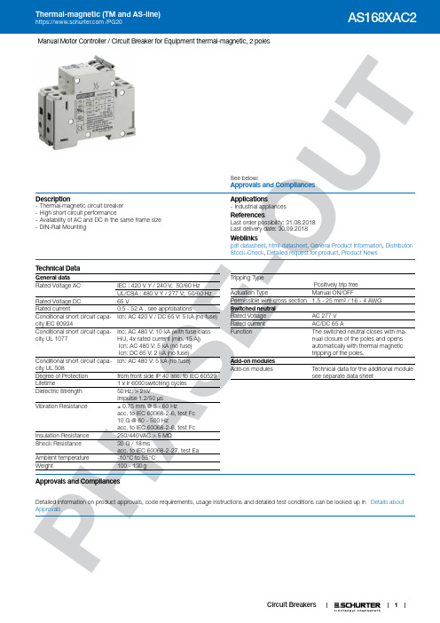
1P HA SE -O U TManual Motor Controller / Circuit Breaker for Equipment thermal-magnetic, 2 polesSee below:Approvals and Compliances Description- Thermal-magnetic circuit breaker - High short circuit performance- Availability of AC and DC in the same frame size - DIN-Rail MountingApplications - Industrial appliancesReferences Last order possibility: 31.08.2018Last delivery date: 30.09.2018Weblinkspdf datasheet , html-datasheet , General Product Information , Distributor-Stock-Check , Detailed request for product , Product NewsT echnical DataGeneral data Rated Voltage AC IEC : 420 V Y / 240 V; 50/60 Hz ␣UL/CSA : 480 V Y / 277 V; 50/60 Hz Rated Voltage DC 65 VRated current0.5 - 52 A , see approbationsConditional short circuit capa-city IEC 60934Icn: AC 420 V / DC 65 V: 5 kA (no fuse)Conditional short circuit capa-city UL 1077Inc: AC 480 V: 10 kA (with fuse class H/J, 4x rated current (min. 15 A)) Icn: AC 480 V: 5 kA (no fuse) Icn: DC 65 V: 2 kA (no fuse)Conditional short circuit capa-city UL 508Icn: AC 480 V: 5 kA (no fuse) Degree of Protection from front side IP 40 acc. to IEC 60529Lifetime 1 x Ir 6000 switching cycles Dielectric Strength 50 Hz: > 2 kVImpulse 1.2/50 μsVibration Resistance ± 0.75 mm @ 5 - 60 Hzacc. to IEC 60068-2-6, test Fc 10 G @ 60 - 500 Hzacc. to IEC 60068-2-6, test FcInsulation Resistance 250/440 VAC > 5 M ΩShock Resistance 30 G / 18 msacc. to IEC 60068-2-27, test EaAmbient temperature -10 °C to 55 °C Weight 100 - 130 gTripping TypePositively trip freeActuation Type Manual ON/OFFPermissible wire cross section 1.5 - 25 mm² / 16 - 4 AWG Switched neutral Rated Voltage AC 277 V Rated current AC/DC 65 A Function The switched neutral closes with ma-nual closure of the poles and opensautomatically with thermal magnetic tripping of the poles.Add-on modules Add-on modules Technical data for the additional modulesee separate data sheetApprovals and CompliancesDetailed information on product approvals, code requirements, usage instructions and detailed test conditions can be looked up in Details about Approvals2P HA SE -O U TApprovalsThe approval mark is used by the testing authorities to certify compliance with the safety requirements placed on electronic products. Approval Reference T ype: AS168XApproval LogoCertificates Certification Body DescriptionVDE Approvals VDEVDE Certificate Number: 40005743UL Approvals UL UL File Number: E216629 / E71572UL ApprovalsULUL File Number: E216629 / E71572Product standardsProduct standards that are referencedOrganizationDesignStandardDescriptionDesigned according to IEC 60934Circuit-breakers for equipment (CBE)Designed according to UL508, UL1077Standard for Supplementary Protectors for Use in Electrical Equipment Designed according to UL 508Standard for Industrial Control Equipment Designed according toCSA C22.2Supplementary Protectors Application standardsApplication standards where the product can be usedOrganizationDesignStandardDescriptionDesigned for applications acc.IEC/UL 60950IEC 60950-1 includes the basic requirements for the safety of information technologyequipment.CompliancesThe product complies with following Guide LinesIdentificationDetailsInitiatorDescriptionCE declaration of conformitySCHURTER AG The CE marking declares that the product complies with the applicable requirements laid down in the harmonisation of Community legislation onits affixing in accordance with EU Regulation 765/2008.RoHSSCHURTER AGEU Directive RoHS 2011/65/EUChina RoHS SCHURTER AG The law SJ / T 11363-2006 (China RoHS) has been in force since 1 March2007. It is similar to the EU directive RoHS.REACHSCHURTER AGOn 1 June 2007, Regulation (EC) No 1907/2006 on the Registration, Evaluation, Authorization and Restriction of Chemicals 1 (abbreviated as "REACH") entered into force.PDimension [mm]AS168X 2 poleA) 35 mm DIN rail EN 50022B) Max. torqueWire crosssection Max. torque1.5 ... 10 mm22.5 Nm16 ... 25 mm2 3.1 NmAWG #16 ... 8 20 ... 22 lb–inAWG #6 ... 4 26 ... 28 lb–inAS168X 2 pole and switched neutral poleA) 35 mm DIN rail EN 50022B) Max. torqueWire crosssection Max. torque1.5 ... 10 mm22.5 Nm16 ... 25 mm2 3.1 NmAWG #16 ... 8 20 ... 22 lb–inAWG #6 ... 4 26 ... 28 lb–in34PHS-U Diagrams AS168X-CB1...AS168X-CB1...NAS168X-CB1... / AS168X-ACBH1AS168X-CB1... / AS168X-ACBH2AS168X-CB1... / AS168X-ACBS1AS168X-CB1... / AS168X-ACBS2AS168X-CB1... / AS168X-ACBA5P HA SE-U Effect of ambient temperatureAC-breaker are calibrated for an ambient temperature of +40°C, DC-breakers for +23°C. To determine the rated current for a lower or6P HA SE -O U TAmpere-HorsepowerHorsepower(FLA & LRC Ratings Apply where no HP Rating is given)Nominal Circuit Voltage, VACAS168X-CBMotor Nameplate110-120200208220-240265277380-415440-480Rated Current (See Note #1)FLA Rating Starting/LRC Rating 2 pole 1 pole0.5A 0.5A 1A 1A 1.5A 1.5A 2A 2A 3A 3A 4A 4A 5A 5A 6A 6A 7A 7A 8A 8A 9A 9A 10A 10A 12A 12A 13A 13A 15A 15A 16A 16A 18A 18A 20A 20A 23A 23A 25A 25A 27A 27A 30A30AAS168X-CB Nominal Circuit Voltage, VAC110-120200208220-240380-415440-480Rated Current(See Note #1)Note #1: For AC motor circuit nameplate FLA loads, AC general-use loades, AC resistance loadsFLA Starting/ 3 pole 0.5A 0.5A 1A 1A 1.5A 1.5A 1/22A 2A 3/43A 3A 1 1/24A 4A 25A 5A 36A 6A 37A 7A 38A 8A 59A 9A 510A 10A 512A 12A 7 1/213A 13A 7 1/215A 15A 1016A 16A 1018A 18A 1020A 20A 1023A 23A 1525A 25A 1527A 27A 2030A 30A20Motor NameplateHorsepower(FLA & LRC Ratings Apply where no HP Rating is given)Rating LRC Rating10A 1/212.5A 3/420A 1/2 1/2 1/2 125A 3/4 3/4 3/4 1 1/232A 1/2 1 1 1 232A 1/2 1 1 1/2 232A 3/4 1/2 1/2 2 346A 3/4 2 2 2 346A 1 2 2 2 346A 1 2 2 3 563.5A 1 1/2 3 3 3 563.5A 1 1/2 3 3 3 581A 2 3 3 3 7 1/281A 2 3 3 5 7 1/281A 2 5 5 5 1081A 3 5 5 5 10116A 3 5 5 7 1/2 10116A 3 5 7 1/2 7 1/2 10145A 3 7 1/2 7 1/2 7 1/2 15145A3 7 1/2 7 1/2 10 153°6° 1/109° 1/10 1/10 1/10 1/612A 1/8 1/6 1/6 1/418A 1/10 1/6 1/6 1/4 1/4 1/3 1/3 1/224A 1/8 1/4 1/3 1/3 1/3 1/3 1/2 130A 1/6 1/3 1/3 1/2 1/2 1/2 3/4 1 1/236A 1/4 1/2 1/2 1/2 3/4 3/4 1 242A 1/4 1/2 1/2 3/4 1 1 1 1/2 248A 1/3 3/4 3/4 1 1 1 2 254A 1/3 3/4 1 1 1 1 1/2 2 360A 1/2 1 1 1 1/2 1 1/2 2 2 372A 1/2 1 1/2 1 1/2 2 2 2 3 378A 1/2 1 1/2 1 1/2 2 2 2 3 390A 3/4 2 2 2 3 3 3 596A 1 2 2 2 3 3 3 5108A 1 2 2 3 3 3 5 5120A 1 1/2 3 3 3 3 3 5 5138A 1 1/2 3 3 3 3 3 5 7 1/2150A 2 3 3 3 5 5 5 7 1/2162A 2 3 3 3 5 5 7 1/2 10180A2 3 3 5 5 5 7 1/2107P H-Time-Current-Curves Version F / Magnetic 3-5 xl nT i m e i n S e c o n d snMultiple of Rated Current InReference Temperature +23°Version G / Magnetic 6-10 xl nT i m e i n S e c o n d snMultiple of Rated Current InReference Temperature +23°Version H / Magnetic 12-20 xl nT i m e i n S e c o n d sMultiple of Rated Current InReference Temperature +23°Config. CodeAS168X-CB 1DG |200|N |The characters are placeholders for the correspondingly keys of selections from the key tables.AS168X-CB 1 DG |200|N | = Number of Poles8-O AS168X-CB 1 DG 200N = Tripping characteristicsAS168X-CB |1|DG | 200 |N | = Rated currentAS168X-CB |1|DG |200| N | = Switched neutralVariants9P HA SE -OPackaging Unit 1 PcsThe specifications, descriptions and illustrations indicated in this document are based on currentinformation. All content is subject to modifications and amendments. Information furnished is believed 19.02.2018。
Keysight B2900B BL Series Precision Source Measure

B2900B/BL SeriesPrecision Source/Measure Unit Cost-effective source/measurement solutions offer superior performanceConfigure Your Keysight B2900B/BL Series Precision Source/Measure UnitThe Keysight B2900B/BL Series Source/Measure Unit (SMU) series contains the following six models. •B2901BL Precision Source/Measure Unit, 1 ch, 1pA resolution, 21 V, 1.5 A•B2910BL Precision Source/Measure Unit, 1 ch, 10fA resolution, 210 V, 1.5 A•B2901B Precision Source/Measure Unit, 1 ch, 100fA resolution, 210 V, 3A DC/10.5 A pulse•B2902B Precision Source/Measure Unit, 2 ch, 100fA resolution, 210 V, 3A DC/10.5 A pulse•B2911B Precision Source/Measure Unit, 1 ch, 10fA resolution, 210 V, 3A DC/10.5 A pulse•B2912B Precision Source/Measure Unit, 2 ch, 10fA resolution, 210 V, 3A DC/10.5 A pulseThis configuration guide has step-by-step instructions to help you configure an SMU and its related accessories to meet specific test requirements. For detailed specifications, refer to the B2900B/BL SMU series data sheet.Step 1. Select B2900B/BL Series modelThere are two key parameters you need to select up-front: the number of measurement channels (one or two) and the SMU performance level. The B2900B/BL series comes in value (B2901BL/B2910BL), standard (B2901B/B2902B) and high-performance (B2911B/B2912B) versions.Note: After purchase it is not possible to upgrade an SMU to have more channels or to the other version.The following items are supplied standard with each B2900B/BL series SMU:Step 2. Select optional accessoriesStep 2-1. Choose a rack mount kit (optional)Step 2-2. Determine if you need to make 4-wire or guarded measurementsThe B2900B/BL SMUs support both 2-wire and 4-wire measurement. The default connection scheme is the simpler 2-wire configuration, which uses only the force terminals. In 2-wire mode the sense terminals are left open.If you are measuring very small resistances or applying very large currents then you should use the 4-wire measurement method (also known as the Kelvin method). This technique uses both the force and sense terminals, and by making the measurement through the sense terminals (in which no current is flowing) the effects of cable resistance are eliminated.Low current measurements (< 1 nA) require guarding to prevent leakage through the measurement cable. The schematic shown below provides a simplified overview of the guarding technique. Guarded measurements require the use of triaxial cables. A follower (x1) buffer amplifier keeps the guardconductor at the same potential as the center conductor. Since there is no voltage difference, no current can flow from the center conductor to the guard.Note: In this example, even the test fixture has a guarded shield to prevent leakage at the test fixture.1. Unguarded 2-Wire connection schemegreater than ± 42 V.Combo test lead kitKelvin probe setU8201ADUT11059A(Max.voltage: ± 42 V)DUTgreater than ± 42 V.3. Guarded 2-Wire connection schemeRecommended connectionDUTU8201AU8201AU8201ADUT DUT16494A-00116494A-001N1297A N1295AThe N1295A does not support Voltages greater than ± 42 V.The 16442B supports Voltages up to 200 V.DUT16442BSMU1 Sense2 Force (Force)16494A-001N1297ASMU 1 SMU 216494A-00111059A(Max.voltage: ± 42 V)Recommended connectionTypical connection exampleRecommended accessories 16494A-0013ea Low leakage Triaxial cable (1.5 m)N1297B 1ea Banana - Triaxial Adapter for 4-wire (Kelvin) connection 16442B1eaTest Fixture for general useStep 2-3. Consider interlock circuit (optional)To prevent accidental exposure to dangerously high voltages, the SMUs have a safety interlock. They cannot source voltages greater than ± 42 V unless the interlock circuit is closed. This is achieved using pins 16 and 24 on the rear Digital I/O output. Normally, these pins are routed to a shielding box or test fixture that must be closed to complete the interlock circuit.If you are using the 16442B test fixture then you can use the N1294A-011 or 012 interlock cables toconnect to the interlock circuit. If you are not using the 16442B then you should install an interlock circuit as shown in the figure below. For more detailed information, please refer to “Installing the Interlock Circuit” in the Keysight Series User’s Guide.DUTSMU 1SMUSence(Force) ForceGuard16494A-001N1297B16494A-00116442B 1 23Step 2-4. Determine if you use the series with multiple software control options (optional)The series has multiple software control options, allowing you to choose the solution that best fits your particular application.•82357B GPIB-USB Interface is required for software control through GPIB interface.• 1.8 m USB cable is furnished with the B2900B/BL series for software control through USB interface. •LAN cable is required for software control through LAN interface.•The EasyEXPERT group+ software supports multiple unit control with synchronization. Please see the next page in detail.Step 2-5. Determine if you use the B2900B/BL SMUs with EasyEXPERT group+ softwareThe EasyEXPERT group+ software is capable to control up to 4 units of the B2900B/BL SMUs at the same time. It is required to make a connection of trigger lines in order to synchronize one unit to the others when you use multiple units of the B2900B/BL SMUs with the EasyEXPERT group+ software. GPIB, USB or LAN connection can use to synchronize multiple units with N1294A-032.1. Use a single unit of the B2900B/BL SMUB2900B/BL 1ea Precision Source/Measure Unit USB/GPIB interface2. Use a two unit of the B2900B/BL SMUB2900B/BL 2ea Precision Source/Measure Unit Digital I/O Trigger Cable for Multiple Unit Control3. Use a three unit of the B2900B/BL SMUB2900B/BL 3ea Precision Source/Measure Unit Digital I/O Trigger Cable for Multiple Unit Control82357B82357BN1294A-032 10833D 82357BN1294A-03210833D4. Use 4 units of the B2900B/BL SMUsB2900B/BL 4ea Precision Source/Measure Unit 1ea USB/GPIB interfaceDigital I/O Trigger Cable for Multiple Unit ControlThe EasyEXPERT group+ software manuals (User’s Guide) are available for download from/find/easyexpert . If you need printed manuals then they can be ordered using the part numbers shown below.Step 2-6. Select additional accessories (optional)The following optional accessories are available for specialized requirements.82357BN1294A-03210833DStep 3. Select warranty length and calibration plan (optional)Keysight factory calibration is provided as standard and free of additional charges.Find us at Page 11Find us at Page 12 This information is subject to change without notice. © Keysight Technologies, 2020 - 2023, Published in USA, May 2, 2023, 3120-1524.EN Learn more at: For more information on Keysight Technologies’ products, applications or services,please contact your local Keysight office. The complete list is available at:/find/contactusSoftware Upgrade Package for B2900B/BL SeriesIf you don’t have the license for the EasyEXPERT group+ software or latest functions on GUI with your existing B2900B/BL Series, a product update may be required. Please contact Keysight in detail. DescriptionProduct number Additional InformationB2901BL software upgrade packageB2901BLU Extension support and subscription B2910BL software upgrade packageB2910BLU B2901B software upgrade packageB2901BU B2902B software upgrade packageB2902BU B2911B software upgrade packageB2911BU B2912B software upgrade packageB2912BU。
M95512-R中文资料
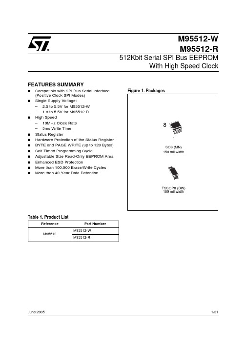
Figure 1. Packages
8 1
SO8 (MN) 150 mil width
TSSOP8 (DW) 169 mil width
Table 1. Prodt Number
M95512
M95512-W M95512-R
June 2005
1/31
元器件交易网
SUMMARY DESCRIPTION . . . . . . . . . . . . . . . . . . . . . . . . . . . . . . . . . . . . . . . . . . . . . . . . . . . . . . . . . . . 5 Figure 2. Logic Diagram . . . . . . . . . . . . . . . . . . . . . . . . . . . . . . . . . . . . . . . . . . . . . . . . . . . . . . . . . . 5 Figure 3. SO and TSSOP Connections . . . . . . . . . . . . . . . . . . . . . . . . . . . . . . . . . . . . . . . . . . . . . . 5 Table 2. Signal Names . . . . . . . . . . . . . . . . . . . . . . . . . . . . . . . . . . . . . . . . . . . . . . . . . . . . . . . . . . 5
■ Single Supply Voltage: – 2.5 to 5.5V for M95512-W – 1.8 to 5.5V for M95512-R
RUZ-092424中文资料

40 20 0
121515 241515
Efficiency %
20 0
0%
20%
40%
60%
80%
100%
0%
20%
40%
60%
80%
100%
Total Output current (%)
Total Output current (%)
Deviation / Load
25.000 20.000 25.000 20.000
元器件交易网
Features
Unregulated Converters
● ● ● ● ● ● ● ●
Dual Output from a Single Input Rail Input/Output Isolation 1kVDC Output/Output Isolation 1kVDC Power Sharing on Outputs UL94V-0 Package Material Toroidal Magnetics No Extern. Components Required Efficiency to 85%
ECONOLINE
DC/DC-Converter
RUZ Series
Selection Guide
Part Number SIP 7 RUZ-xx3.33.3 RUZ-xx0505 RUZ-xx0509 RUZ-xx0512 RUZ-xx0515 RUZ-xx0909 RUZ-xx1212 RUZ-xx1515 RUZ-xx2424 xx = Input Voltage Input Voltage (VDC) 5, 9, 12, 24 5, 9, 12, 24 5, 9, 12, 24 5, 9, 12, 24 5, 9, 12, 24 5, 9, 12, 24 5, 9, 12, 24 5, 9, 12, 24 5, 9, 12, 24 Output Voltage (V1VDC) 3.3 5 5 5 5 9 12 15 24 Output Voltage (V2VDC) 3.3 5 9 12 15 9 12 15 24 Output Current (mA) 303/303 200/200 200/111 200/84 200/66 111/111 84/84 66/66 42/42 Efficiency (%) 70 70-82 70-82 70-82 70-82 82-84 82-84 82-84 80-85
Airmar TRIDUCER 产品说明书

35 Meadowbrook Drive, Milford, New Hampshire 03055-4613USA Tel (603) 673-9570 • Fax (603) 673-4624 • e-mail: sales@airmar .comAIRMARTECHNOLOGY CORPORATIONm 122000#17-1205B744V , B744VL,SS544V , B66V , B66VL50 kHz,120 kHz, 120 kHz Dual Beam, 150 kHz, 170 kHz, 200 kHz, 235 kHz,50/200 kHz Dual Frequency,50 kHz & 200 kHz Dual FrequencyU.S. Patent No. 4,898,029U.S. Patent No. 5,186,050Canadian Patent No. 1,313,775Australian Patent No. 605,281Japanese Patent No. 1851014Airmar TRIDUCER ® multisensors incorpo-rate a revolutionary self-closing valve to min-imize water flow into the boat when thepaddlewheel insert is removed. “Gushers” are eliminated with this simple to maintain valve.Fins provide on either side of the paddlewheel for more accurate speed measurement in cross-flow conditions.Combined with our fairing, installation is made simple. Made of urethane, the fairing will never swell or rot, and the unique cutting guide allows safer, more accurate cutting with a band saw. High speed fairings are provided with a corrosion resistant bolt to secure the fairing and prevent rotation.Specifications• Hall-effect device senses paddlewheel rotation• Unitary paddlewheel bearing assures exact alignment and minimal rotational friction• Corrosion-proof shaft for long life in saltwater• Alignment key for easy speed/temperature assembly removal and insertion in difficult access locations • Replaceable valve assembly• Polished paddlewheel shaft for quick start up • Surge and reverse polarity protection• Shielded cable to minimize noise pick-up and emission • Designed to meet CE requirements • Dual O-rings for superior sealing• Retaining pin and safety chain secures paddlewheel and plug inserts • Installation requires a 51mm (2") diameter hole • Fairing is supplied standard with SS544V • Blanking plug included• Standard cable length: 10 m (33')• Weight:B744V 2.5 kg (5.5 lb.)B744VL 2.6 kg (6.4 lb.)SS544V 3.1 kg (6.8 lb..)B66V 2.7 kg (6.0 lb.)B66VL 3.1 kg (6.8 lb.) Options• Two wire speed sensor circuit• Thermistor or semiconductor temperature sensor • Urethane fairingB744V , B744VL: High speed #33-353-01B66V , B66VL: Standard #33-029• Pulse division circuitry or other pulse rates • CS4500 correlation speed/temperature insertSelf-closing valve ...checks water flow when paddlewheel insert is removedNew B744V and long stem B744VL offer flush mounting in streamlined fairings and accommodate ceramics up to 44 mm (1.75 " ) in diameter including the popular 50/200 kHz modelSS544 includes a streamlined fairing and is designed specifically for isolatedmounting to steel and aluminum hulls. It accommodates ceramics up to 44 mm (1.75 " ) in diameterNew streamlined fairings for B744V , B744VL, and SS544V provide much improved echosounding at speeds above 20 knots and greatly reduce dragVersatile B66V and long stem B66VL mounts frequencies varying from 50 kHz to 200 kHz including dual beam 120 kHz and dual element 50 kHz & 200 kHz Optional paddlewheel-less speed/temperature sensor uses echo correlation technologySS544VB66V B66VLB744VThe Latest Evolution in TRIDUCER ™ Multisensor TechnologyAIRMARTECHNOLOGY CORPORATION35 Meadowbrook Drive, Milford, New Hampshire 03055-4613 USA Tel (603) 673-9570 • Fax (603) 673-4624 • e-mail: sales@airmar .comm 132000#17-1205SpeedThe TRIDUCER ® multisensor provides accurate speed measurement over the widest boat speed range of any thru-hull paddlewheel transducer.The combination of a hydrodynamic paddlewheel and paddlewheel cav-ity, housing and fairing projection through the boundary layer and fins on either side of the paddlewheel gives an unmatched linearity.TemperatureVarious temperature sensing devices can be incorporated in the housing including ther-mistor and semiconductor types. See the “Temperature” section for more detailed information including thermal time constants.ShieldingInside the TRIDUCER ® multisensor housing, shielding is used to eliminate interference between the speed and depth sensors. A shielded cable and separately shielded speed and temperature conductors are used to pre-vent mutual interference. The bronze housing also functions as a shield. Refer to wiring dia-gram beginning on p 35 for shielding details.Applications • Fiberglass or wood hulls onlyNotes• Replaces B44, B50, B55, and B56 models• For Parts and Accessories see pages p2 through p4Single Connector/Dual Connector SystemsThe piezoceramic element, speed, and temperature cir-cuitry are all within the bronze housing. The removable paddlewheel insert contains no circuitry. The magnetic field sensor to measure speed is mounted in the housing in close proximity to the rotating paddlewheel. A single con-nector system is generally used when depth, speed, and temperature will be processed in a single instrument or when two instruments are within 1m (40") of each other. When depth and speed/temperature functions will be pro-cessed in separate instruments, our cable can be split and two connectors can be applied.All signals are transmitted via a multi-conductor cable with a high quality thermoplastic rubber jacket forimproved resistance to cutting, pinching, and degradation from petroleum distillates. C144 cable is used in single element TRIDUCER ® multisensors. Dual element multi-sensors use C145 cable.New Specifications 11. Refer to “Sensor Design Fundementals” for more detailed information.Speed range 22. Requires correction for non-linearity below 3 knots (3MPH).1–44 knots (1–50 MPH)LinearityRefer to Airmar Technical Data CatalogPulse rate (B744V ,B744VL,SS544V)19,000 ppnm 3 (5.7 Hz/knot) with high speed fairing 21,500 ppnm 3 (6.0 Hz/knot) without fairing 3. ppnm = pulses per natical mile.Pulse rate (B66V , B66VL)21,500 ppnm 3 (6.0 Hz/knot) with standard fairing 21,500 ppnm 3 (6.0 Hz/knot) without fairing Supply voltage 5–25 VDC Supply current: “OFF”“ON” 2.3 mA 8 mA at 5 VDC Circuitry: standardoptional 3 wire format 2 wire format Unicurve® type thermistor10,000 ohmsHull Thickness LimitsModelMinimumMaximumB744V with fairing —26 mm (1")without fairing 6 mm (1⁄4")72 mm (2 7⁄8")B744VL with fairing 6 mm (1⁄4")87 mm (3 3⁄4")without fairing 35 mm (1 3⁄8")133 mm (5 1⁄4")SS544V with fairing —14 mm (1⁄2")B66V with fairing —25 mm (1”)without fairing 6 mm (1⁄4")70 mm (2 3⁄4") B66VL with fairing 30 mm (1 1⁄8")87 mm (3 3⁄4")without fairing70 mm (2 3⁄4")133 mm (5 1⁄4")35 Meadowbrook Drive, Milford, New Hampshire 03055-4613 USA Tel (603) 673-9570 • Fax (603) 673-4624 • e-mail: sales@airmar .comAIRMARTECHNOLOGY CORPORATIONm 142000#17-1205NewB744VSS544V High-speed SS544VFairingFairingB744V, B744VL High-speedAIRMARTECHNOLOGY CORPORATION35 Meadowbrook Drive, Milford, New Hampshire 03055-4613 USA Tel (603) 673-9570 • Fax (603) 673-4624 • e-mail: sales@airmar .comm 152000#17-1205insert and Paddlewheel plugblanking B66V, B66VLStandard Fairing35 Meadowbrook Drive, Milford, New Hampshire 03055-4613 USA Tel (603) 673-9570 • Fax (603) 673-4624 • e-mail: sales@airmar .comTECHNOLOGY CORPORATIONm 162000#17-1205TRIDUCER ® MultisensorfinsAIRMARTECHNOLOGY CORPORATION35 Meadowbrook Drive, Milford, New Hampshire 03055-4613 USA Tel (603) 673-9570 • Fax (603) 673-4624 • e-mail: sales@airmar .comm 172000#17-1205B744VExploded View35 Meadowbrook Drive, Milford, New Hampshire 03055-4613 USA Tel (603) 673-9570 • Fax (603) 673-4624 • e-mail: sales@airmar .comAIRMARTECHNOLOGY CORPORATIONm 182000#17-1205Note: See page m 1 for footnotes.* Unbalanced ImpedanceP ERFORMANCE D ATAFrequency 1 – Airmar Piezoceramic Designator 250 kHz – C 120 kHz – B 120 kHz – C 120 kHz – M Dual Beam Element Material 3/ Diameter (mm)PZT/L / 51PZT/37PZT/51PZT/L /19PZT/L /55Beam Width at –3 dB 46°16°12°35°14°Q (fr/∆ f @ –3 dB)4182121915Rated RMS Power (W)600300600100600Voltage Responses: Transmit/Receive 5 (dB)156/–175161/–181166/–174152/–188167/–180Figure of Merit (Insertion Loss)6 (dB)–27–25–18–37–16Balanced Impedance 7:Resistance, Rp (ohm)Capacitance, C p (pF)28012260150615*150*08601,5102,200*4,100*S eries Impedance [R – jX]8 (ohm)280 – j0250 – j40150 – j20300 – j310110 – j50Acoustic Window MaterialUrethaneUrethaneUrethaneUrethaneUrethaneFREQUENCY AVAILABILITY by HOUSING TYPECeramic DesignationBeam Width @–3dBHousingB744VB744VLSS544VB66VB66VL50 kHz – C 46°••120 kHz – B 16°•••120 kHz – C 12°••120 kHz – M (dual beam)35° & 14°••150 kHz – A 19°•••170 kHz – A 12°••200 kHz – G 8°••200 kHz – Hlq 8°••200 kHz – U 11°•••235 kHz – B 11°•••235 kHz – D7°••50/200 kHz – A (dual frequency)45° & 12°•••50 kHz – C & 200 kHz – B(dual frequency)46° & 13°••AIRMARTECHNOLOGY CORPORATION35 Meadowbrook Drive, Milford, New Hampshire 03055-4613 USA Tel (603) 673-9570 • Fax (603) 673-4624 • e-mail: sales@airmar .comm 192000#17-1205Note: See page m1 for footnotes.P ERFORMANCE D ATAFrequency 1 – Airmar Piezoceramic Designator 2235 kHz – B 235 kHz – D 50/200kHz – A50 kHz – C & 200 kHz – B Element Material 3/Diameter (mm)PZT /36BT /51PZT/44PZT/ L / 51BT/28Beam Width at –3 dB 11°7°45°12°46°13°Q (fr/∆ f @ –3 dB)4251628311822Rated RMS Power (W)350600600600600250Voltage Responses: Transmit/Receive 5 (dB)165/–186169/–185155/–174164/–184156/–175162/–187Figure of Merit (Insertion Loss)6 (dB)–21–16–31–21–27–26Balanced Impedance 7:Resistance, Rp (ohm)Capacitance, C p (pF)350370190410280125104101,4407207200560S eries Impedance [R – jX]8 (ohm)330 – j70220 – j180175 – j40360 – j130280 – j0450 – j160Acoustic Window MaterialUrethaneUrethane UrethaneUrethaneUrethaneNote: See page m 1 for footnotes.*Unbalanced ImpedanceP ERFORMANCE D ATAFrequency 1 – Airmar Piezoceramic Designator 2150 kHz – A 170 kHz – A 200 kHz – G 200 kHz – Hlq 11200 kHz – U Element Material 3/Diameter (mm)PZT/27PZT/51BT/51PZT/51BT/38Beam Width at –3 dB 19°12°8°8°11°Q (fr/∆ f @ –3 dB)4232529722Rated RMS Power (W)200500600600375Voltage Responses: Transmit/Receive 5 (dB)160/–185172/–184167/–182163/–182164/–185Figure of Merit (Insertion Loss)6 (dB)–27–17–16–19–22Balanced Impedance 7:Resistance, Rp (ohm)Capacitance, C p (pF)4007012370865510*55001,1201,2001,930*S eries Impedance [R – jX]8 (ohm)380 – j8070 – j0290 – j150325 – j420300 – j250Acoustic Window MaterialUrethaneUrethaneUrethaneUrethaneUrethane。
瑞特拉电子产品购买指南说明书
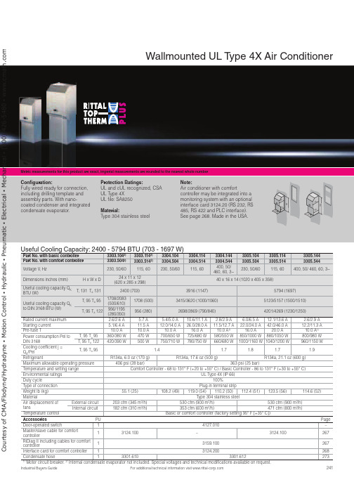
241For additional technical information visit Metric measurements for this product are exact, imperial measurements are rounded to the nearest whole numberUseful Cooling Capacity: 2400 - 5794 BTU (703 - 1697 W)Part No. with basic controller 3303.1042)3303.1142)3304.1043304.1143304.1443305.1043305.1143305.144Part No. with comfort controller 3303.5042)3303.5142)3304.5043304.5143304.5443305.5043305.5143305.544Voltage V , Hz230, 50/60115, 60230, 50/60115, 60400, 50/ 460, 60, 3~230, 50/60115, 60400, 50/ 460, 60, 3~Dimensions inches (mm)H x W x D24 x 11 x 12 (620 x 285 x 298)40 x 16 x 14 (1020 x 405 x 358)Useful cooling capacity Q KBTU (W)T i 131 T a 1312400 (703)3916 (1147)5794 (1697)Useful cooling capacity Q K to DIN 3168 BTU (W)T i 95 T a 951708/2083(500/610)1708 (500)3415/3620 (1000/1060)5123/5157 (1500/1510)T i 95 T a 122956/1195(280/350)956 (280)2698/2869 (790/840)4201/4269 (1230/1250)Rated current maximum 2.6/2.6 A 5.7 A 5.4/5.0 A 10.6/11.1 A 2.8/2.9 A 6.0/6.5 A 12.1/13.6 A 2.6/2.9 A Starting current 5.1/6.4 A 11.5 A 12.0/14.0 A 26.0/28.0 A 11.5/12.7 A 22.0/24.0 A 42.0/46.0 A 12.2/11.3 A Pre-fuse T 10.0 A 10.0 A 10.0 A 16.0 A 10.0 A 1)16.0 A 20.0 A 10.0 A 1)Power consumption Pel toDIN 3168T i 95 T a 95360/380 W 470 W 700/650 W 725/680 W 580/550 W 850/1000 W 880/1050 W 800/980 W T i 95 T a 122420/390 W500 W 750/710 W 780/750 W 660/680 W 1000/1160 W 1040/1200 W 960/1150 W Cooling coefficient j =Q K /PelT i 95 T a 95 1.4 1.7 1.8 1.7 1.9Refrigerant R134a, 6.0 oz (170 g)R134a, 17.6 oz (500 g)R134a, 21.1 oz (600 g)Maximum allowable operating pressure 406 psi (28 bar)363 psi (25 bar)Temperature and setting range Comfort Controller - 68 to 131° F (+20 to +55° C) / Basic Controller - 86 to 131° F (+30 to +55° C)Environmental ratings UL Type 4X (IP 66)Duty cycle 100%Type of connection Plug-in terminal strip Weight lb (kg)55.1 (25)108.2 (49)119.0 (54)110.2 (50)112.4 (51)123.5 (56)114.6 (52)Material Type 304 stainless steelAir displacement offans External circuit 203 cfm (345 m 3/h)530 cfm (900 m 3/h)530 cfm (900 m 3/h)Internal circuit 182 cfm (310 m 3/h)353 cfm (600 m 3/h)471 cfm (800 m 3/h)Temperature control Basic or comfort controller (factory setting 95° F [+35° C])Accessories PU Page Door-operated switch 14127.010–Master/slave cable for comfortcontroller13124.100–3124.100267RiDiag II including cables for comfortcontroller13159.100267Interface card for comfort controller 13124.200268Condensate hose 13301.6103301.6122731) Motor circuit breaker. 2)Internal condensate evaporator not included. Special voltages and technical modifications available on request.Wallmounted UL T ype 4X Air ConditionerCon guration:Fully wired ready for connection, including drilling template and assembly parts. With nano-coated condenser and integrated condensate evaporator.Protection Ratings:UL and cUL recognized, CSA UL Type 4XUL file: SA8250 Material:Type 304 stainless steel Note:Air conditioner with comfortcontroller may be integrated into a monitoring system with an optional interface card 3124.20 (RS 232, RS 485, RS 422 and PLC interface). See page 268. Made in the USA.000C o u r t e s y o f C M A /F l o d y n e /H y d r a d y n e ŀ M o t i o n C o n t r o l ŀ H y d r a u l i c ŀ P n e u m a t i c ŀ E l e c t r i c a l ŀ M e c h a n i c a l ŀ (800) 426-5480 ŀ w w w .c m a f h .c o242For additional technical information visit Metric measurements for this product are exact, imperial measurements are rounded to the nearest whole numberUseful Cooling Capacity: 8706 - 10525 BTU (2550 - 3083 W)Part No. with basic controller 3328.1043328.1143328.1443329.1043329.1143329.144Part No. with comfort controller 3328.5043328.5143328.5443329.5043329.5143329.544Rated operating voltage V , Hz 230, 50/60115, 50/60400, 50/460, 60, 3~230, 50/60115, 50/60400, 50/460, 60, 3~Dimensions inches (mm)H x W x D 65 x 16 x 15 (1650 x 405 x 388)Useful cooling capacity Q K BTU (W)T i 131 T a 1318706 (2550)10525 (3083)Useful cooling capacity Q K to DIN 3168 BTU (W)T i 95 T a 956860/8025 (2000/2350)8538/9392 (2500/2750)T i 95 T a 1224952/5772 (1450/1690)5464/5977 (1600/1750)Rated current max. 7.5 A/9.1 A 14.7 A/17.3 A 2.8 A/3.3 A 8.6 A/10.6 A 17.0 A/22.0 A 3.7 A/3.8 A Start-up current 22.0 A/26.0 A36.0 A/39.0 A6.8 A/7.8 A 21.0 A/21.0 A44.0 A/42.0 A6.8 A/7.6 A Pre-fuse T16.0 A25.0 A 10.0A/10.0 A 1)16.0 A 25.0 A 10.0 A/10.0 A 1)Power consumption Pel to DIN 3168 T i 95 T a 951025/1200 W 1085/1250 W 1050/1275 W 1450/1675 W 1500/1725 W 1425/1625 W T i 95 T a 1221250/1350 W1300/1410 W1275/1525 W1625/2000 W1675/2065 W1675/1975 WCooling coefficient j = Q K /Pel T i 95 T a 951.72.31.92.0RefrigerantR134a, 31.7 oz (900 g)Maximum allowable operating pressure 406 psi (28 bar)Temperature and setting range Comfort Controller - 68 to 131° F (+20 to +55° C) / Basic Controller - 86 to 131° F (+30 to +55° C)Protection rating UL Type 4X (IP 66)Duty cycle 100%Type of connection Plug-in terminal stripWeight lb (kg)176.4 (80)191.8 (87)176.4 (80)183.0 (83)198.4 (90)183.0 (83)MaterialType 304 stainless steelAir displacement of fans External circuit 377 cfm (640 m 3/h)418 cfm (710 m 3/h)Internal circuit324 cfm (550 m 3/h)377 cfm (640 m 3/h)Temperature control Basic or comfort controller (factory setting 95° F [+35° C])Accessories PU Page Door-operated switch14127.010–Master/slave cable for comfort controller13124.100267RiDiag II including cables for comfort controller 13159.100267Interface card for comfort controller 13124.200268Condensate hose13301.6122731)Motor circuit breaker. Special voltages available on request. We reserve the right to make technical modifications.Wallmounted UL T ype 4X Air ConditionerCon guration:Fully wired ready for connection, including drilling template and assembly parts. With nano-coated condenser and integrated condensate evaporator.Protection Ratings: UL and cUL recognized UL Type 4X UL file: SA8250Material:Type 304 stainless steelNote:Air conditioner with comfortcontroller may be integrated into a monitoring system with an optional interface card 3124.200(RS 232, RS 485, RS 422 and PLC interface). See page 268. Made in the USA.C o u r t e s y o f C M A /F l o d y n e /H y d r a d y n e ŀ M o t i o n C o n t r o l ŀ H y d r a u l i c ŀ P n e u m a t i c ŀ E l e c t r i c a l ŀ M e c h a n i c a l ŀ (800) 426-5480 ŀ w w w .c m a f h .c o。
VDZT2R5.1B;中文规格书,Datasheet资料
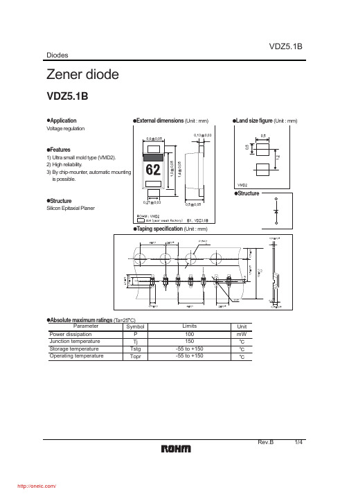
Diodes
Zener diode
VDZ5.1B
zApplication Voltage regulation zExternal dimensions (Unit : mm) 㩷
㪇㪅㪍㫧㪇㪅㪇㪌 㪇㪅㪈㪊㫧㪇㪅㪇㪊
zLand size figure (Unit : mm)
㪇㪅㪌 㪇㪅㪌
Appendix
Notes
No technical content pages of this document may be reproduced in any form or transmitted by any means without prior permission of ROHM CO.,LTD. The contents described herein are subject to change without notice. The specifications for the product described in this document are for reference only. Upon actual use, therefore, please request that specifications to be separately delivered. Application circuit diagrams and circuit constants contained herein are shown as examples of standard use and operation. Please pay careful attention to the peripheral conditions when designing circuits and deciding upon circuit constants in the set. Any data, including, but not limited to application circuit diagrams information, described herein are intended only as illustrations of such devices and not as the specifications for such devices. ROHM CO.,LTD. disclaims any warranty that any use of such devices shall be free from infringement of any third party's intellectual property rights or other proprietary rights, and further, assumes no liability of whatsoever nature in the event of any such infringement, or arising from or connected with or related to the use of such devices. Upon the sale of any such devices, other than for buyer's right to use such devices itself, resell or otherwise dispose of the same, no express or implied right or license to practice or commercially exploit any intellectual property rights or other proprietary rights owned or controlled by ROHM CO., LTD. is granted to any such buyer. Products listed in this document are no antiradiation design.
迪杰尔电子产品说明书

0 110 .
110
pfllq —q sue m
‘1111
g1wg
1011
110u1m 03101 10 p an g 01100
1,108u11
1101011311011] 0111011
°0101s 001 p 001q 110100111111
S H“ ,
11011 011011
5 1101,831101 10 110110X u u 11011 é xp p ol 15011) 10
sh o es
b
o
o
t
s .
D o n ot p ut m y b o o ts n e a r
th e fire .
C an y ou ge t th e se sh o es
b o ots h e ele d
so le d
W 1 m en d e d ?
l h e re is th e b o y to sh ow
‘.10mm 11110 A p q
3010011 101110, 1 1ss0 B -0 0110110111 101
111A
101
“ 93131013118011
- 01&1110s1ds 01110 151 11A 801 10 1901110011 011011 011131111 1
11111101193m um 118A
1 2113031
- Old 111 001 80 11011 1101111 - 11001q 10101101111100 10111111
im n e S k o o
S
tflv
le
r .
dd-wrt固件支持的路由器型号
Pronghorn Metro SBC
-
?
Xscale IXP425@533
64
16
-
depends on card
4
1
?
1 LAN, 1 WAN
yes
17- 30 & 36- 60
CF socket, hw watchdog, temp. and volt. sensor
mini PCI
Serial port
JTAG port
Eth. port count
PoE
Volt. Input [V/A]
Special Features Notes
min required DD-WRT version
Notes for Running DD-WRT
Coyote
-
?
Xscale IXP425@533
v.24 sp2 - build 12646 - 13/08/09
MI424WR
MI424WR
C
LNQ802MAG
Xscale IXP425@533
32
8
depends on card
Atheros b/g
1
1
1
4 LAN 1 WAN
-
5V / 3A
OEM'd to Verizon, FIOS port will not work
clone ofdir-300
V24 RC5
[1]
AP431W
?
RRK-AP431W
Atheros AR2313A@180
16
4
Atheros
b/g
Altech Corp. FUSE BLOCKS 5 x 20 和 5 x 25 mm 商品说明书

FUSE BLOCKS, 5 x 20 and 5 x 25 mm®• 35 Royal Road • Flemington, NJ 08822-6000 • Phone (908)806-9400 • FAX (908)806-9490 18SCREW TERMINAL BLOCKSFUSE BLOCKSWidthApprovalsHeight w DIN Rail8 mm50.3 mm57.6 mm50.3 mm57.6 mmCF4UDimensions & WeightTechnical Data/RatingsInstallation InstructionsTerminal BlocksCF4U(L)/6-60V8 mmLength57.0 mm57.0 mmWeight per piece14.8 g15.4 gWire Size (solid / stranded)22-10 AWG0.2-4 mm222-10 AWG0.2-4 mm2Voltage Rating600 V800 V AC/DC 600 V800 V AC/DCScrewdriver Flat Head 0.6 x 3.5 mm Flat Head 0.6 x 3.5 mmCurrent Rating10 A 6.3 A10 A 6.3 AInsulation Material Polyamide 66Polyamide 66Torque7 lb-in0.5 Nm7 lb-in0.5 NmWire Stripping Length9.5 mm9.5 mmDIN Rail251112020CA701-15/S20251116010AccessoriesFuses5 x 20 mmStd. Pk.251112020CA701-15/S20251116010Std. Pk.Cat. No.Cat. No.Std. Pk.Std. Pk.Cat. No.Cat. No.External Jumper CA711/2 100CA711/3 50CA711/4 50CA711/10 202 pole3 pole4 pole10 poleCA711/2 100CA711/3 50CA711/4 50CA711/10 2060947-7-360947-7-3MT8 1 Pk. (100 tags)MT6 1 Pk. (100 tags)Marking Tag MT8 1 Pk. (100 tags)MT6 1 Pk. (100 tags)50.3 mm57.6 mmCF4U(L)/110-240V8 mm57.0 mm15.4 g22-10 AWG0.2-4 mm2600 V800 V AC/DCFlat Head 0.6 x 3.5 mm10 A 6.3 APolyamide 667 lb-in0.5 Nm9.5 mm251112020CA701-15/S20251116010Std. Pk.Cat. No.Std. Pk.Cat. No.CA711/2 100CA711/3 50CA711/4 50CA711/10 2060947-7-3MT8 1 Pk. (100 tags)MT6 1 Pk. (100 tags) HIGHLIGHTStypes•Completely enclosed, noendplates•CF4U(L)version with LEDfor blown fuse indication•Large marking area•No polarity required•Blocks can be used for AC& DC VoltagesAPPLICATIONS•Control systems with fuseprotectionFuse SpecificationsGrey (standard)Blue BUBlack BLCF4U(L)/110-240V50CF4U(L)/110-240V/BU50CF4U(L)/110-240V/BL505x20 mm / 5 x 25 mm5x20 mm / 5 x 25 mm-6-60V AC/DC5x20 mm / 5 x 25 mm110-240V AC/DCOn TerminalOn Fuse Carrier27KΩ220KΩCurrent Slow Blow Fast BlowRating Cat. No Cat. No0.1A 0.1M5x20T 0.1M5x20F0.2A 0.2M5x20T 0.2M5x20F0.5A 0.5M5x20T 0.5M5x20F1.0A 1.0M5x20T 1.0M5x20F2.0A 2.0M5x20T 2.0M5x20F4.0A 4.0M5x20T 4.0M5x20F5.0A 5.0M5x20T 5.0M5x20F6.3A 6.3M5x20T 6.3M5x20F8.0A 8.0M5x20T 8.0M5x20F10.0A 10.0M5x20T 10.0M5x20FØ5mm(0.2 in.)2mm(.79in.)E220514E220514E220514FUSE BLOCKS, 5 x 20 and 5 x 25 mm®• 35 Royal Road • Flemington, NJ 08822-6000 • Phone (908)806-9400 • FAX (908)806-949019SCREW TERMINAL BLOCKSWidth ApprovalsHeight w DIN Rail 35 x 7.5 mm35 x 15 mm 6 mm 70.0 mm 77.5 mm 70.0 mm 77.5 mm CF4SPDimensions & WeightInstallation InstructionsTerminal BlocksCF4SP(L)/6-60V6 mm Length58.5 mm 58.5 mm Weight per piece16.9 g17.4 gWire Size (solid / stranded)24-10 AWG 0.2-4 mm 224-10 AWG 0.2-4 mm 2Voltage Rating 600 V 1000 V AC/DC600 V 1000 V AC/DCScrewdriverFlat Head 0.6 x 3.5 mm Flat Head 0.6 x 3.5 mm Current Rating 10 A 10 A 10 A 10 A Insulation MaterialPolyamide 66Polyamide 66Torque4.5 lb-in0.5 Nm4.5 lb-in0.5 NmWire Stripping Length 8 mm8 mmDIN Rail251112020CA701-15/S 20251116010AccessoriesStd. Pk.251112020CA701-15/S 20251116010Std. Pk.Cat. No.Cat. No.Std. Pk.Std. Pk.Cat. No.Cat. No.External JumperCA714/2 100CA714/3 100CA714/4 100CA714/10 202 pole 3 pole 4 pole 10 pole CA714/2 100CA714/3 100CA714/4 100CA714/10 2060947-7-360947-7-3MT6 1 Pk. (100 tags)MT6 1 Pk. (100 tags)Marking TagMT6 1 Pk. (100 tags)MT6 1 Pk. (100 tags)70.0 mm 77.5 mm CF4SP(L)/110-240V6 mm 58.5 mm 17.4 g24-10 AWG 0.2-4 mm 2600 V 1000 V AC/DCFlat Head 0.6 x 3.5 mm 10 A10 A Polyamide 664.5 lb-in0.5 Nm8 mm251112020CA701-15/S 20251116010Std. Pk.Cat. No.Std. Pk.Cat. No.CA714/2 100CA714/3 100CA714/4 100CA714/10 2060947-7-3MT6 1 Pk. (100 tags)MT6 1 Pk. (100 tags)Fuse SpecificationsGrey (standard) Blue BU Black BLCF4SP(L)/110-240V 50CF4SP(L)/110-240V/BU50CF4SP(L)/110-240V/BL50Fuse Type5x20 mm / 5 x 25 mm5x20 mm / 5 x 25 mmLED Indicator Voltage-6-60V AC/DC5x20 mm / 5 x 25 mm 110-240V AC/DCOn Terminal On Fuse Carrier27K Ω220K ΩInternal JumperCA722/2 100CA722/3 100CA722/4 100CA722/10 10CA722/100 102 pole 3 pole 4 pole 10 pole 100 pole CA722/2 100CA722/3 100CA722/4 100CA722/10 10CA722/100 10InsulatedInternal JumperCA742/2 100CA742/3 100CA742/4 100CA742/10 10CA742/100 102 pole 3 pole 4 pole 10 pole 100 pole CA742/2 100CA742/3 100CA742/4 100CA742/10 10CA742/100 10CA722/2 100CA722/3 100CA722/4 100CA722/10 10CA722/100 10CA742/2 100CA742/3 100CA742/4 100CA742/10 10CA742/100 10 HIGHLIGHTS。
PHILIPS WP3922 说明书

飛利浦水龍頭式淨水器專用的更換濾芯Micro X-Pure輕鬆享受純淨好水Micro X-Pure 濾芯先進過濾系統利用中空絲膜與離子交換體,去除細菌、有害的有機化合物、氯氣與鉛金屬,改善口感與氣味,並保留水中有益的礦物質。
純淨好水•去除細菌、水溶鉛與有害的有機化合物輕鬆享受•先進的 Quick Twist 機制讓您輕鬆地更換濾芯發行日期 2010-12-25版本: 3.7.112 NC: 0000 000 00000© 2010 Koninklijke Philips Electronics N.V.所有權利均予保留。
規格若有變更恕不另行通知。
商標為 Koninklijke Philips Electronics N.V. 或其個別所有者的財產。
規格水龍頭式淨水器專用的更換濾芯Micro X-Pure焦點Micro X-Clean 濾芯Micro X-Clean 為一多重過濾系統。
由以下元件組成:高科技中空絲膜,內含超過 3000 億個微毛孔,可有效清除 99.99% 的細菌;離子交換體,可去除有害的水溶性鉛;微細粒狀活性碳,可去除加氯消毒後所產生的有害副產物、有害工業污染物 (例如揮發性有機化學物),以及 CAT 殺蟲劑等農業污染物。
Micro X-Clean 也可去除惱人的氯氣、臭味與異味。
濾芯會保留飲水中對人類健康極為重要的有益礦物質。
Quick Twist 更換濾芯先進的 Quick Twist 濾芯更換機制讓您迅速、輕鬆又安全地更換濾芯,將智慧與簡易帶入淨水器。
一般規格•水流量: 5 度•水流量: 1.6 l/min設計規格•顏色: 白色•產品重量: 180 g•產品尺寸 (長 x 寬 x 高): 60 x 64 x 105 公釐•材料: 塑膠濾水系統•除菌: 99.99 %•除氯: >75 %•懸浮物去除: 3000 公升或大約 1 年•去除 VOC (揮發性有機化合物)•去除赫爾蒙•去除殺蟲劑濾芯規格•濾芯壽命: 1500 公升或約 3 個月•主要濾芯組件: 中空絲膜, 粒狀活性碳 (GAC), 離子交換器, 前置沉澱濾芯輸入水環境•最低輸入水壓: 0.7 棒•最高輸入水壓: 3.5 棒•最高輸入水溫: 50 度產地•替換濾網: 日本永續性•包裝: > 90% 為再生材料。
AD229b基本介绍

诊断型听力计技术参数(AD229B)基本介绍 主要特点:1. 125Hz-8,000Hz共11个测试频点2. -10dB-120dBHL输出3. 气导、骨导和言语测试4. 言语测试自动评分5. 白噪声、窄带噪声和言语噪声等掩蔽信号6. 言语和纯音的自由声场测试7. 5dB、1dB电平步进8. 标准的TDH39气导耳机9. 自动听阈测试10. 啭音和脉冲音11. 通话提示和通话应答12. SISI、ABLB、Stenger和Bekesy测试13. 同侧掩蔽(Langenbeck)14. 可实现PC在线监控15. 真正的RMS电平表16. 内置监听扬声器17. DSP技术18. 可接PC的RS232接口19. 触摸式给音方式20. NOAH兼容技术规格安全标准:EN60601-1听力计标准:纯音:EN60645-1,ANSI S3.6,2型。
言语:EN60645-2,ANSI S3.6,B型。
CE医疗认证:认证证书号0123。
校准:气导:ISO 389-1(TDH39),骨导:389-3。
输出电平:-10至120dBHL,1dB、5dB步进(125Hz最大输出90dB、250Hz和8KHz最大输出110dB)输入:纯音、啭音±5%,5Hz输出:左,右,骨导左+右,插入式耳机,插入掩蔽,FF1,FF2,儿童声场扬声器PLS5。
传导器件:TDH39耳机,EAR-Tone 3A插入式耳机,B71骨导器。
通讯:提示通话:0-110dBSPL在面板上连续可调。
应答通话:在面板上可控制麦克风输入和电平调节。
信号发射:自动或手动。
单脉冲、连续脉冲,通/断。
自动听阈测试:病人控制的基于ISO8253-1的Hughson-Westlake法或基于NIOSH的OSHA法。
同步掩蔽:可锁定通道2的掩蔽信号与通道1同步增减。
存储功能:内存可存储一次完整的测试结果。
(气导L/R、骨导L/R、言语)显示:阿尔法-数字式显示。
美国拓尔普斯Amprobe耐用的实时电阻传感器阴管温度计说明书

Data SheetRTD Thermometer WirelessThe RTD probes are preferred for industrial process applications. They typically provide higher accuracy than thermocouples and maintain stability for many years.RTD-10WWireless two-way transmissionRTD dual input functionPt3916/Pt3926/Pt385 RTD standard°C/°F user-selectableMAX/MIN with elapsed time, AVG, REL, HOLD functionsWarning beeper with Hi/Lo settingResolution 0.1°C or 0.2°FData SheetGeneral SpecificationsDisplay4½ digit liquid crystal display (LCD) with maximum reading of 19999.Auto Power Off30 minutes Operating Environment0°C to 50°C (32°F to 122°F) at <70% R.H.Storage Environment-20°C to 60°C (-4°F to 140°F), 0 to 80% R.H. with battery removed from meter.AccuracyStated accuracy at 23°C ±5°C, <75% R.H.Battery1.5V x 4pcs AAA size Battery Life200 hours typical DimensionsL241.3 X W158 X 76.2mm (9.5 X 6.22 X 3 in).WeightApprox. 304g (0.67lb) including batteries and packaging box.WIRELESS FeaturesFrequency Range910~920MHz.Low current consumption less than 1mA.The transmitting distance can reach 25M without magnetic interference. Electrical Specifications:Temperature ScaleCelsius or Fahrenheit user-selectable Measurement RangePt385 (100Ω) -200°C to 800°C (-328°F to 1472°F) Pt3916/Pt3926 (100Ω) -200°C to 630°C(-328°F to 1166°F) Resolution0.1°C or 0.2°F AccuracyAccuracy is specified for operating temperatures over the range of 18°C to 28°C (64°F to 82°F), for 1year, not including thermocouple error. ±(0.05%rdg+0.2°C) on °C scale ±(0.05%rdg+0.4°F) on °F scale Temperature0.1 times the applicable accuracy CoefficientSpecification per °C from 0°C to 18°C and 28°C to 50°C (32°F to 64°F and 82°F to 122°F). Input Protection24V DC or 24V AC rms maximum input Voltage on any combination of input pins. InputAccepts 3 wire or 4 wire Mini-Din ConnectorPlug and meter are designed for standard. The other probes 2.3 wires will cause measuringtolerance due to cable resistance. Included Accessories RTD Connectors (2); users manual; batteries (4); USB wireless antenna; software CD ©2010 Amprobe Test Tools. All rights reserved.6/2010 RTD-10W_DS Rev A Amprobe® Test Toolswebsite: email:****************Everett, WA 98203 Tel: 877-AMPROBERTD-10W RTD Thermometer Wireless。
- 1、下载文档前请自行甄别文档内容的完整性,平台不提供额外的编辑、内容补充、找答案等附加服务。
- 2、"仅部分预览"的文档,不可在线预览部分如存在完整性等问题,可反馈申请退款(可完整预览的文档不适用该条件!)。
- 3、如文档侵犯您的权益,请联系客服反馈,我们会尽快为您处理(人工客服工作时间:9:00-18:30)。
Micropower, Low Noise Precision VoltageReferences with ShutdownADR390/ADR391/ADR392/ADR395 Rev. FInformation furnished by Analog Devices is believed to be accurate and reliable.However, no responsibility is assumed by Analog Devices for its use, nor for anyinfringements of patents or other rights of third parties that may result from its use. Specifications subject to change without notice. No license is granted by implication or otherwise under any patent or patent rights of Analog Devices. Trademarks and registered trademarks are the property of their respective owners.One Technology Way, P.O. Box 9106, Norwood, MA 02062-9106, U.S.A. Tel: Fax: 781.461.3113© 2005 Analog Devices, Inc. All rights reserved.FEATURESCompact TSOT-23-5 packages Low temperature coefficientB grade: 9 ppm/°CA grade: 25 ppm/°CInitial accuracyB grade: ±4 mV maximumA grade: ±6 mV maximumUltralow output noise: 5 µV p-p (0.1 Hz to 10 Hz) Low dropout: 300 mVLow supply current3 µA maximum in shutdown120 µA maximum in operationNo external capacitor requiredOutput current: 5 mAWide temperature range−40°C to + 125°CAPPLICATIONSBattery-powered instrumentationPortable medical instrumentationData acquisition systemsIndustrial process controlsAutomotiveFUNCTIONAL BLOCK DIAGRAMV INV OUT (SENSE)GNDV OUT (FORCE)419-D-1Figure 1. 5-Lead TSOT (UJ Suffix)Table 1.Model V OUT (V)TemperatureCoefficient (ppm/°C) Accuracy (mV) ADR390B 2.048 9 ±4ADR390A 2.048 25 ±6ADR391B 2.5 9 ±4ADR391A 2.5 25 ±6ADR392B 4.096 9 ±5ADR392A 4.096 25 ±6ADR395B 5.0 9 ±5ADR395A 5.0 25 ±6GENERAL DESCRIPTIONThe ADR390, ADR391, ADR392, and ADR395 are precision 2.048 V, 2.5 V, 4.096 V, and 5 V band gap voltage references, respectively, featuring low power and high precision in a tiny footprint. Using ADI’s patented temperature drift curvature correction techniques, the ADR39x references achieve a low 9 ppm/°C of temperature drift in the TSOT package. The ADR39x family of micropower, low dropout voltage references provides a stable output voltage from a minimum supply of 300 mV above the output. Their advanced design eliminates the need for external capacitors, which further reduces board space and system cost. The combination of low power operation, small size, and ease of use makes the ADR39x precision voltage references ideally suited for battery-operated applications.ADR390/ADR391/ADR392/ADR395Rev. F | Page 2 of 20TABLE OF CONTENTSADR390 Specifications....................................................................3 ADR391 Specifications....................................................................4 ADR392 Specifications....................................................................5 ADR395 Specifications....................................................................6 Absolute Maximum Ratings............................................................7 Thermal Resistance......................................................................7 ESD Caution. (7)Terminology.......................................................................................8 Typical Performance Characteristics..............................................9 Theory of Operation......................................................................16 Applications.....................................................................................17 Basic Voltage Reference Connection.......................................17 Outline Dimensions.......................................................................19 Ordering Guide.. (19)REVISION HISTORY5/05—Rev. E to Rev. FChanges to Table 5...........................................................................7 Changes to Figure 2.........................................................................9 4/04—Rev. D to Rev. EChanges to ADR390—Specifications............................................3 Changes to ADR391—Specifications............................................4 Changes to ADR392—Specifications............................................5 Changes to ADR395—Specifications............................................6 4/04—Rev. C to Rev. DUpdated Format................................................................Universal Changes to Title...............................................................................1 Changes to Features.........................................................................1 Changes to Applications.................................................................1 Changes to General Description...................................................1 Changes to Table 1...........................................................................1 Changes to ADR390—Specifications............................................3 Changes to ADR391—Specifications............................................4 Changes to ADR392—Specifications............................................5 Changes to ADR395—Specifications............................................6 Changes to Absolute Maximum Ratings......................................7 Changes to Thermal Resistance.....................................................7 Moved ESD Caution........................................................................7 Changes to Figure 3, Figure 4, Figure 7, and Figure 8................9 Changes to Figure 11, Figure 12, Figure 13, and Figure 14......10 Changes to Figure 15, Figure 16, Figure 19, and Figure 20......11 Changes to Figure 23 and Figure 24............................................12 Changes to Figure 27.....................................................................13 Changes to Ordering Guide.........................................................19 Updated Outline Dimensions......................................................19 10/02—Rev. B to Rev. CAdd parts ADR392 and ADR395....................................Universal Changes to Features........................................................................1 Changes to General Description...................................................1 Additions to Table I.........................................................................1 Changes to Specifications...............................................................2 Changes to Ordering Guide...........................................................4 Changes to Absolute Maximum Ratings......................................4 New TPCs 3, 4, 7, 8, 11, 12, 15, 16, 19, and 20............................6 New Figures 4 and 5......................................................................13 Deleted A Negative Precision Referencewithout Precision Resistors Section............................................13 Edits to General-Purpose Current Source Section...................13 Updated Outline Dimensions......................................................15 5/02—Rev. A to Rev. BEdits to Layout...................................................................Universal Changes to Figure 6.......................................................................13 Revision 0: Initial VersionADR390/ADR391/ADR392/ADR395Rev. F | Page 3 of 20ADR390 SPECIFICATIONSElectrical characteristics, V IN = 2.5 V to 15 V , T A = 25°C, unless otherwise noted. Table 2.Parameter Symbol Conditions Min Typ Max UnitOUTPUT VOLTAGE V O A grade 2.042 2.048 2.054 V V O B grade 2.044 2.048 2.052 V INITIAL ACCURACY V OERR A grade 6 mV V OERR A grade 0.29 % V OERR B grade 4 mV V OERR B grade 0.19 % A grade: −40°C < T A < +125°C25 ppm/°C TEMPERATURE COEFFICIENT TCV O B grade: −40°C < T A < +125°C9 ppm/°C SUPPLY VOLTAGE HEADROOM V IN − V O 300 mV LINE REGULATION ∆V O /∆V IN V IN = 2.5 V to 15 V, −40°C < T A < +125°C 10 25 ppm/V I LOAD = 0 mA to 5 mA, −40°C < T A < +85°C, V IN = 3 V60 ppm/mA LOAD REGULATION ∆V O /∆I LOAD I LOAD = 0 mA to 5 mA, −40°C < T A < +125°C, V IN = 3 V140 ppm/mA No load120 µA QUIESCENT CURRENT I IN −40°C < T A < +125°C140 µA VOLTAGE NOISE en p-p 0.1 Hz to 10 Hz 5 µV p-p TURN-ON SETTLING TIME t R20 µs LONG-TERM STABILITY 1∆V O 1000 hours 50 ppm OUTPUT VOLTAGE HYSTERESIS ∆V O_HYS 100 ppm RIPPLE REJECTION RATIO RRR f IN = 60 kHz 80 dB V IN = 5 V25 mA SHORT CIRCUIT TO GND I SC V IN = 15 V30 mA SHUTDOWN PIN Shutdown Supply Current I SHDN 3 µA Shutdown Logic Input Current I LOGIC 500 nA Shutdown Logic Low V INL 0.8 V Shutdown Logic High V INH2.4 V1The long-term stability specification is noncumulative. The drift of subsequent 1000 hour periods is significantly lower than in the first 1000 hour period.ADR390/ADR391/ADR392/ADR395Rev. F | Page 4 of 20ADR391 SPECIFICATIONSElectrical characteristics, V IN = 2.8 V to 15 V , T A = 25°C, unless otherwise noted. Table 3.Parameter Symbol Conditions Min Typ Max UnitOUTPUT VOLTAGE V O A grade 2.494 2.5 2.506 V V O B grade 2.496 2.5 2.504 V V OERR A grade6 mV INITIAL ACCURACY V OERR Agrade 0.24 % V OERR B grade 4 mV V OERR B grade 0.16 % A grade, −40°C < T A < +125°C25 ppm/°C TEMPERATURE COEFFICIENT TCV O B grade, −40°C < T A < +125°C9ppm/°CSUPPLY VOLTAGE HEADROOM V IN − V O 300 mV LINE REGULATION ∆V O /∆V IN V IN = 2.8 V to 15 V, −40°C < T A < +125°C10 25 ppm/V I LOAD = 0 mA to 5 mA, −40°C < T A < +85°C, V IN = 3 V60 ppm/mA LOAD REGULATION∆V O /∆I LOAD I LOAD = 0 mA to 5 mA, −40°C < T A < +125°C, V IN = 3 V140 ppm/mA No load120 µA QUIESCENT CURRENT I IN −40°C < T A < +125°C140 µA VOLTAGE NOISE en p-p 0.1 Hz to 10 Hz 5 µV p-p TURN-ON SETTLING TIME t R20 µs LONG-TERM STABILITY 1∆V O 1000 hours 50 ppm OUTPUT VOLTAGE HYSTERESIS ∆V O_HYS 100 ppm RIPPLE REJECTION RATIO RRR f IN = 60 kHz 80 dB V IN = 5 V25 mA SHORT CIRCUIT TO GND I SC V IN = 15 V30 mA SHUTDOWN PIN Shutdown Supply Current I SHDN 3 µA Shutdown Logic Input Current I LOGIC 500 nA Shutdown Logic Low V INL 0.8 V Shutdown Logic High V INH2.4 V1The long-term stability specification is noncumulative. The drift of subsequent 1000 hour periods is significantly lower than in the first 1000 hour period.ADR390/ADR391/ADR392/ADR395Rev. F | Page 5 of 20ADR392 SPECIFICATIONSElectrical characteristics, V IN = 4.3 V to 15 V , T A = 25°C, unless otherwise noted. Table 4.Parameter Symbol Conditions Min Typ Max UnitOUTPUT VOLTAGE V O A grade 4.090 4.096 4.102 V V O B grade 4.091 4.096 4.101 V V OERR A grade6 mV INITIAL ACCURACY V OERR Agrade 0.15 % V OERR B grade 5 mV V OERR B grade 0.12 % A grade, −40°C < T A < +125°C25 ppm/°C TEMPERATURE COEFFICIENT TCV O B grade, −40°C < T A < +125°C9 ppm/°C SUPPLY VOLTAGE HEADROOM V IN − V O 300 mV LINE REGULATION ∆V O /∆V IN V IN = 4.3 V to 15 V, −40°C < T A < +125°C 10 25 ppm/V LOAD REGULATION ∆V O /∆I LOAD I LOAD = 0 mA to 5 mA, −40°C < T A < +125°C, V IN = 5 V 140 ppm/mA No load120 µA QUIESCENT CURRENT I IN −40°C < T A < +125°C140 µA VOLTAGE NOISE en p-p 0.1 Hz to 10 Hz 7 µV p-p TURN-ON SETTLING TIME t R 20 µs LONG-TERM STABILITY 1 ∆V O 1000 hours 50 ppm OUTPUT VOLTAGE HYSTERESIS ∆V O_HYS 100 ppm RIPPLE REJECTION RATIO RRR f IN = 60 kHz 80 dB V IN = 5 V25 mA SHORT CIRCUIT TO GND I SC V IN = 15 V30 mA SHUTDOWN PIN Shutdown Supply Current I SHDN 3 µA Shutdown Logic Input Current I LOGIC 500 nA Shutdown Logic Low V INL 0.8 V Shutdown Logic High V INH2.4 V1The long-term stability specification is noncumulative. The drift of subsequent 1000 hour periods is significantly lower than in the first 1000 hour period.ADR390/ADR391/ADR392/ADR395Rev. F | Page 6 of 20ADR395 SPECIFICATIONSElectrical characteristics, V IN = 5.3 V to 15 V , T A = 25°C, unless otherwise noted. Table 5.Parameter Symbol Conditions Min Typ Max UnitOUTPUT VOLTAGE V O A grade 4.994 5.000 5.006 V V O B grade 4.995 5.000 5.005 V V OERR A grade6 mV INITIAL ACCURACY V OERR Bgrade 0.12 % V OERR B grade 5 mV V OERR B grade 0.10 % A grade, −40°C < T A < +125°C25 ppm/°C TEMPERATURE COEFFICIENT TCV O B grade, −40°C < T A < +125°C9 ppm/°C SUPPLY VOLTAGE HEADROOM V IN − V O 300 mV LINE REGULATION ∆V O /∆V IN V IN = 4.3 V to 15 V, −40°C < T A < +125°C 10 25 ppm/V LOAD REGULATION ∆V O /∆I LOAD I LOAD = 0 mA to 5 mA, −40°C < T A < +125°C, V IN = 6 V 140 ppm/mA No load120 µA QUIESCENT CURRENT I IN −40°C < T A < +125°C140 µA VOLTAGE NOISE en p-p 0.1 Hz to 10 Hz 8 µV p-p TURN-ON SETTLING TIME t R 20 µs LONG-TERM STABILITY 1 ∆V O 1, 000 hours 50 ppm OUTPUT VOLTAGE HYSTERESIS ∆V O_HYS 100 ppm RIPPLE REJECTION RATIO RRR f IN = 60 kHz 80 dB V IN = 5 V25 mA SHORT CIRCUIT TO GND I SC V IN = 15 V30 mA SHUTDOWN PIN Shutdown Supply Current I SHDN 3 µA Shutdown Logic Input Current I LOGIC 500 nA Shutdown Logic Low V INL 0.8 V Shutdown Logic High V INH2.4 V1The long-term stability specification is noncumulative. The drift of subsequent 1,000 hour periods is significantly lower than in the first 1,000 hour period.ADR390/ADR391/ADR392/ADR395Rev. F | Page 7 of 20ABSOLUTE MAXIMUM RATINGSAt 25°C, unless otherwise noted. Table 6.Parameter RatingSupply Voltage 18 VOutput Short-Circuit Duration to GND See derating curvesStorage Temperature Range–65°C to +125°C Operating Temperature Range –40°C to +125°C Junction Temperature Range –65°C to +125°C Lead Temperature Range (Soldering, 60 sec)300°CStresses above those listed under Absolute Maximum Ratingsmay cause permanent damage to the device. This is a stress rating only and functional operation of the device at these or any other conditions above those indicated in the operational section of this specification is not implied. Exposure to absolute maximum rating conditions for extended periods may affect device reliability.THERMAL RESISTANCEθJA is specified for the worst-case conditions, that is, θJA is specified for a device soldered in a circuit board for surface-mount packages. Table 7. Thermal ResistancePackage Type θJA θJC Unit TSOT-23-5 (UJ-5)230146 °C/WESD CAUTIONESD (electrostatic discharge) sensitive device. Electrostatic charges as high as 4000 V readily accumulate on the human body and test equipment and can discharge without detection. Although this product features proprietary ESD protection circuitry, permanent damage may occur on devices subjected to high energy electrostatic discharges. Therefore, proper ESD precautions are recommended to avoid performancedegradation or loss of functionality.ADR390/ADR391/ADR392/ADR395Rev. F | Page 8 of 20TERMINOLOGYTemperature CoefficientThe change of output voltage with respect to operating temp-erature changes normalized by the output voltage at 25°C. This parameter is expressed in ppm/°C and can be determined by the following equation:[]()()()()610–25–××°=°12O 1O 2O O T T C V T V T V C /ppm TCVwhere:V O (25°C) = V O at 25°C V O (T 1) = V O at Temperature 1 V O (T 2) = V O at Temperature 2Line RegulationThe change in output voltage due to a specified change in input voltage. This parameter accounts for the effects of self-heating. Line regulation is expressed in either percent per volt, parts-per-million per volt, or microvolts per volt change in input voltage.Load RegulationThe change in output voltage due to a specified change in load current. This parameter accounts for the effects of self-heating. Load regulation is expressed in either microvolts per milli-ampere, parts-per-million per milliampere, or ohms of dc output resistance.Long-Term StabilityTypical shift of output voltage at 25°C on a sample of parts subjected to a test of 1,000 hours at 25°C.∆V O = V O (t 0) – V O (t 1)[]()()()⎟⎟⎠⎞⎜⎜⎝⎛×=∆610–0O 1O 0O O t V t V t V ppm V where:V O (T 0) = V O at 25°C at Time 0V O (T 1) = V O at 25°C after 1,000 hours operation at 25°CThermal HysteresisThe change of output voltage after the device is cycled through temperatures from +25°C to –40°C to +125°C and back to +25°C. This is a typical value from a sample of parts put through such a cycle.V O_HYS = V O (25°C) – V O_TC[]()61025–25×°°=C V V C V ppm V O O_TCO O_HYSwhere:V O (25°C) = V O at 25°CV O_TC = V O at 25°C after a temperature cycle from + 25°Cto –40°C to +125°C and back to +25°C NOTESInput CapacitorInput capacitors are not required on the ADR39x. There is no limit for the value of the capacitor used on the input, but a 1 µF to 10 µF capacitor on the input improves transientresponse in applications where the supply suddenly changes. An additional 0.1 µF in parallel also helps reduce noise from the supply.Output CapacitorThe ADR39x does not require output capacitors for stability under any load condition. An output capacitor, typically 0.1 µF, filters out any low level noise voltage and does not affect the operation of the part. On the other hand, the load transient response can improve with the addition of a 1 µF to 10 µFoutput capacitor in parallel. A capacitor here acts as a source of stored energy for a sudden increase in load current. The only parameter that degrades by adding an output capacitor is the turn-on time, and it depends on the size of the capacitor chosen.–150D R I F T (p p m )150TIME (Hours)0–100–5050100100200300400500600700100000419-D -002900800Figure 2. ADR391 Typical Long-Term Drift over 1,000 HoursADR390/ADR391/ADR392/ADR395Rev. F | Page 9 of 20TYPICAL PERFORMANCE CHARACTERISTICSTEMPERATURE (°C)2.040O U T P U T V O L T A G E (V )2.0442.0482.0522.0562.06000419-D -003Figure 3. ADR390 Output Voltage vs. Temperature 2.494V O U T (V )2.4962.4982.5002.5022.5042.50600419-D -004TEMPERATURE (°C)Figure 4. ADR391 Output Voltage vs. Temperature TEMPERA TURE (°C)–404080125V O U T(V )00419-D -005Figure 5. ADR392 Output Voltage vs. Temperature 5.006–40–53065125V O U T (V )5.0045.0025.0004.9964.9944.99810000419-D -006TEMPERATURE (°C)Figure 6. ADR395 Output Voltage vs. TemperatureINPUT VOLTAGE (V)140120402.515.05.0S U P P L Y C U R R E N T (µA )7.510.012.51008060+125°C+25°C–40°C00419-D -007+85°CFigure 7. ADR390 Supply Current vs. Input VoltageINPUT VOLTAGE (V)140120402.515.05.0S U P P L Y C U R R E N T (µA )7.510.012.51008060+85°C+25°C–40°C00419-D -008Figure 8. ADR391 Supply Current vs. Input VoltageADR390/ADR391/ADR392/ADR395Rev. F | Page 10 of 20INPUT V OL T AGE (V)5791115S U P P L Y C U R R E N T (µA )1300419-D -009Figure 9. ADR392 Supply Current vs. Input Voltage INPUT VOLTAGE (V)5.57.08.510.014.5S U P P L Y C U R R E N T (µA )13.011.500419-D -010Figure 10. ADR395 Supply Current vs. Input Voltage TEMPERATURE (°C)L O A D R E G U L A T I O N (p p m /m A )2040608010012000419-D -011Figure 11. ADR390 Load Regulation vs. TemperatureTEMPERATURE (°C)80L O A D R E G U L A T I O N (p p m /m A )10012014016018000419-D -012Figure 12. ADR391 Load Regulation vs. TemperatureTEMPERA TURE (°C)90–40–53065125L O A D R E G U L A T I O N (p p m /m A )8070504060100Figure 13. ADR392 Load Regulation vs. TemperatureTEMPERA TURE (°C)–40–53065125L O A D R E G U L A T I O N (p p m /m A )10000419-D -014Figure 14. ADR395 Load Regulation vs. TemperatureTEMPERATURE (°C)0–40–10L I N E R E G U L A T I O N (p p m /V )208011012525510152000419-D -01550Figure 15. ADR390 Line Regulation vs. Temperature TEMPERATURE (°C)0L I N E R E G U L A T I O N (p p m /V )25510152000419-D -016–40–10208011012550Figure 16. ADR391 Line Regulation vs. TemperatureTEMPERA TURE (°C)–40–53065125L I N E R E G U L A T I O N (p p m /V )10000419-D -017Figure 17. ADR392 Line Regulation vs. Temperature TEMPERA TURE (°C)14–40–53065125L I N E R E G U L A T I O N (p p m /V )10620410012800419-D -018Figure 18. ADR395 Line Regulation vs. TemperatureLOAD CURRENT (mA)3.02.001V I N _M I N (V )2342.62.42.2–40°C+85°C+25°C00419-D -01952.8+125°CFigure 19. ADR390 Minimum Input Voltage vs. Load CurrentLOAD CURRENT (mA)3.62.6013.43.22.8–40°C+85°C+25°CV I N _M I N (V )00419-D -02023453.0+125°CFigure 20. ADR391 Minimum Input Voltage vs. Load CurrentLOAD CURRENT (mA)4.81235V I N _M I N (V )4.44.03.84.244.6+125°C+25°C–40°C00419-D -021Figure 21. ADR392 Minimum Input Voltage vs. Load Current LOAD CURRENT (mA)6.001235V I N _M I N (V )5.24.84.65.045.6+125°C+25°C–40°C5.85.400419-D -022Figure 22. ADR395 Minimum Input Voltage vs. Load CurrentV OUT DEVIATION (mV)6050F R E Q U E N C Y40302010Figure 23. ADR390 V OUT Hysteresis Distribution V OUT DEVIATION (mV)70500F R E Q U E N C Y403020106000419-D -024Figure 24. ADR391 V OUT Hysteresis DistributionFREQUENCY (Hz)1k100V O L T A GE N O I S E D E N S I T Y (n V H z )00419-D -025Figure 25. Voltage Noise Density vs. FrequencyV O L T A G E (2µV /D I V )TIME (1 Sec/DIV)00419-D -026Figure 26. ADR391 Typical Voltage Noise 0.1 Hz to 10 HzV O L T A G E (100µV/D I V )TIME (10µs/DIV)Figure 27. ADR391 Voltage Noise 10 Hz to 10 kHz V O L T A G ETIME (10µs/DIV)00419-D -028Figure 28. ADR391 Line Transient Response V O L T A G ETIME (10µs/DIV)00419-D -029Figure 29. ADR391 Line Transient ResponseV O L T A G E (1V /D I V)TIME (200µs/DIV)00419-D -030Figure 30. ADR391 Load Transient ResponseV O L T A G E (1V /D I V)TIME (200µs/DIV)Figure 31. ADR391 Load Transient ResponseV O L T A G E (1V /D I V)TIME (200µs/DIV)00419-D -032Figure 32. ADR391 Load Transient ResponseV O L T A G ETIME (20µs/DIV)00419-D -033Figure 33. ADR391 Turn-On Response Time at 15 V V O L T A G ETIME (40µs/DIV)00419-D -034Figure 34. ADR391 Turn-Off Response at 15 V V O L T A G ETIME (200µs/DIV)00419-D -035Figure 35. ADR391 Turn-On/Turn-Off Response at 5 VV O L T A G ETIME (200µs/DIV)00419-D -036Figure 36. ADR391 Turn-On/Turn-Off Response at 5 VV O L T A G E (5V /D I V )TIME (200µs/DIV)00419-D -037Figure 37. ADR391 Turn-On/Turn-Off Response at 5 VFREQUENCY (Hz)101M100R I P P L E R E J E C T I O N (d B )1k 10k 100k8060–12040200–20–40–60–80–10000419-D -038Figure 38. Ripple Rejection vs. FrequencyFREQUENCY (Hz)O U T P U T I M P E D A N C E (Ω)100900807060504030201000419-D -039Figure 39. Output Impedance vs. FrequencyTHEORY OF OPERATIONBand gap references are the high performance solution for low supply voltage and low power voltage reference applications, and the ADR390/ADR391/ADR392/ADR395 are no exception. The uniqueness of these devices lies in the architecture. As shown in Figure 40, the ideal zero TC band gap voltage is referenced to the output, not to ground. Therefore, if noise exists on the ground line, it is greatly attenuated on V OUT . The band gap cell consists of the PNP pair, Q51 and Q52, running at unequal current densities. The difference in V BE results in a voltage with a positive TC, which is amplified by a ratio ofR54R582×This PTAT voltage, combined with V BE s of Q51 and Q52, produces a stable band gap voltage.Reduction in the band gap curvature is performed by the ratio of the resistors R44 and R59, one of which is linearlytemperature dependent. Precision laser trimming and other patented circuit techniques are used to further enhance the drift performance.V INV OUT (FORCE)V OUT (SENSE)GND00419-D -040Figure 40. Simplified SchematicDEVICE POWER DISSIPATION CONSIDERATIONSThe ADR390/ADR391/ADR392/ADR395 are capable of deli-vering load currents to 5 mA, with an input voltage that ranges from 2.8 V (ADR391 only) to 15 V . When these devices are used in applications with large input voltages, care should be taken to avoid exceeding the specified maximum powerdissipation or junction temperature because it could result in premature device failure. The following formula should be used to calcu-late a device’s maximum junction temperature or dissipation:JAA J D T –T P θ=In this equation, T J and T A are, respectively, the junction and ambient temperatures. P D is the device power dissipation, and θJA is the device package thermal resistance.SHUTDOWN MODE OPERATIONThe ADR390/ADR391/ADR392/ADR395 include a shutdown feature that is TTL/CMOS level compatible. A logic low or a zero volt condition on the SHDN pin is required to turn the devices off. During shutdown, the output of the referencebecomes a high impedance state, where its potential would then be determined by external circuitry. If the shutdown feature is not used, the SHDN pin should be connected to V IN (Pin 2).APPLICATIONSBASIC VOLTAGE REFERENCE CONNECTIONThe circuit shown in Figure 41 illustrates the basic configuration for the ADR39x family. Decoupling capacitors are not required for circuit stability. The ADR39x family is capable of driving capacitive loads from 0 µF to 10 µF. However, a 0.1 µF ceramic output capacitor is recommended to absorb and deliver the charge, as required by a dynamic load.00419-D -041Figure 41. Basic Configuration for the ADR39x FamilyStacking Reference ICs for Arbitrary OutputsSome applications may require two reference voltage sources, which are a combined sum of standard outputs. Figure 42 shows how this stacked output reference can be implemented.OUT2OUT1V 00419-D -042Figure 42. Stacking Voltage References with theADR390/ADR391/ADR392/ADR395Two reference ICs are used, fed from an unregulated input, V IN . The outputs of the individual ICs are simply connected in series, which provides two output voltages, V OUT1 and V OUT2. V OUT1 is the terminal voltage of U1, while V OUT2 is the sum of this voltage and the terminal voltage of U2. U1 and U2 are simply chosen for the two voltages that supply the required outputs (see the Output Table in Figure 42). For example, if both U1 and U2 are ADR391s, V OUT1 is 2.5 V and V OUT2 is 5.0 V . While this concept is simple, a precaution is required. Since the lower reference circuit must sink a small bias current from U2 plus the base current from the series PNP output transistor in U2, either the external load of U1 or R1 must provide a path for this current. If the U1 minimum load is not well defined, the R1 resistor should be used and set to a value that will conservatively pass 600 µA of current with the applicable V OUT1 across it. Note that the two U1 and U2 reference circuits are treated locally as macrocells; each has its own bypasses at input and output for best stability. Both U1 and U2 in this circuit can source dc currents up to their full rating. The minimum input voltage, V IN , is determined by the sum of the outputs, V OUT2, plus the dropout voltage of U2.A Negative Precision Reference without Precision ResistorsA negative reference can be easily generated by adding an A1 op amp and is configured as shown in Figure 43. V OUTF and V OUTS are at virtual ground and, therefore, the negative reference can be taken directly from the output of the op amp. The op amp must be dual-supply, low offset, and rail-to-rail if the negative supply voltage is close to the reference output.DD–V REF00419-D -043Figure 43. Negative Reference。