EFM32GG980F512,EFM32GG980F1024,EFM32GG980F1024,EFM32GG980F1024, 规格书,Datasheet 资料
Silicon Labs智能物联网关键应用Workshop
汽车与工业设备 保健与医疗设备
• 挡风玻璃除雾 • 气候控制 • 空气压缩系统
• 呼吸治疗 • 呼吸仪 • 药物存储
13
Silicon Labs Confidential
传感器: 使用Si702x非常容易
原理图
装配
Si702x仅需3要个外部元件 完全适合SMT的拾放与回流
工厂校准 工业级低功耗 高精度±3%RH / 0.4°C 工业标准引脚和软件接口 可选的保护膜
12
Silicon Labs Confidential
传感器——相对湿度与温度的应用
智能家居与消费 类设备
远程监测
• 恒温器 • 气象站 • 手机配件
• 通信机柜与 数据中心
• 资产追踪
Cortex M3 Up to 48 MHz Flash: 64-256 RAM: 32
Cortex M3 Up to 48 MHz Flash: 512-1024 RAM: 128
Cortex M4 Up to 48 MHz Flash: 64-256 RAM: 32
Silicon Labs Confidential
7
7
Silicon Labs Confidential
IoT 目前在智能工业的应用 传感器网络| 接口 | 电机控制
8
8
Silicon Labs Confidential
IOT正处于一个重要的市场机会阶段, Silicon Labs可提供一套完整的解决方案
9
9
Silicon Labs Confidential
全球8功能集成度最高的微控制器
Flash Memory (KB)
1024 128 4 2
LTE-M Expansion Kit用户指南说明书
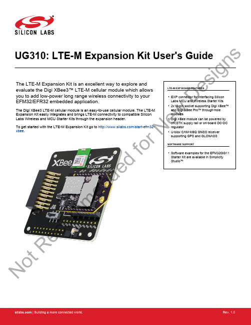
UG310: LTE-M Expansion Kit User's GuideThe LTE-M Expansion Kit is an excellent way to explore and evaluate the Digi XBee3™ LTE-M cellular module which allows you to add low-power long range wireless connectivity to your EFM32/EFR32 embedded application.The Digi XBee3 LTE-M cellular module is an easy-to-use cellular module. The LTE-M Expansion Kit easily integrates and brings LTE-M connectivity to compatible Silicon Labs Wireless and MCU Starter Kits through the expansion header.To get started with the LTE-M Expansion Kit go to /start-efm32-xbee .LTE-M EXP BOARD FEATURES•EXP connector for interfacing Silicon Labs MCU and Wireless Starter Kits •2x10-pin socket supporting Digi XBee™and Digi XBee Pro™ through-hole modules•Digi XBee module can be powered by (W)STK supply rail or on-board DC-DC regulator•U-blox CAM-M8Q GNSS receiver supporting GPS and GLONASSSOFTWARE SUPPORT•Software examples for the EFM32GG11Starter Kit are available in Simplicity Studio™No tR e co mme nd edf or N e wDe si g n sTable of Contents1. Introduction................................32. Hardware Overview .. (4)2.1 Hardware Layout . (4)3. Connectors (5)3.1 EXP Header...............................53.1.1 Pass-through EXP Header ........................63.1.2 EXP Header Pinout ...........................63.2 Digi XBee Module Socket ..........................73.2.1 Digi XBee Module Socket Pinout ......................83.2.2 Power Supply ....... (9)4. Using the LTE-M Expansion Kit (10)4.1 Board Identification............................104.2 Digi XBee3 LTE-M Module ..........................104.3 On-Board GNSS Receiver .................. (11)5. Schematics, Assembly Drawings, and BOM (13)6. Kit Revision History (14)6.1 SLEXP8021A Revision History ..................... (14)7. Document Revision History (15)No tR e co mme nd edf or N e wDe si g n s1. IntroductionThis user guide covers the usage of the Silicon Labs LTE-M EXP Board together with the Digi XBee3 LTE-M cellular module. The LTE-M EXP Board is designed to be compatible with all Digi XBee through-hole modules offering a wide array of wireless connectivity op-tions, such as Zigbee, Wi-Fi, 3G and LTE cellular to name a few.Software examples demonstrating how to use the LTE-M Expansion Kit with the EFM32GG11 Starter Kit are available through Simplici-ty Studio™.For more information about the Digi XBee modules see https:///xbee .IntroductionNo tR e co mme nd edf or N e wDe si g n s2. Hardware Overview2.1 Hardware LayoutThe layout of the LTE-M Expansion Kit is shown in the figure below.EXP-header for Starter KitsPower source select switchPass-through EXP-headerNot mountedDigi XBee Module ResetDigi XBee Module SocketDigi XBee Module Breakout HeaderNot mountedDigi XBee Module Breakout HeaderFigure 2.1. LTE-M Expansion Kit Hardware LayoutHardware OverviewNo tR e co mme nd edf or N e wDe si n s3. ConnectorsThis chapter gives an overview of the LTE-M Expansion Kit connectivity and power connections.EXP HeaderEXP Header (Not Mounted)(Not Mounted)(Not Mounted)Figure 3.1. LTE-M Expansion Kit Connector Layout3.1 EXP HeaderOn the left side of the LTE-M Expansion Kit, a right-angle female 20-pin EXP header is provided to allow connection to one of Silicon Labs’ MCU or Wireless Starter Kits. The EXP header on the Starter Kits follows a standard which ensures that commonly used periph-erals such as an SPI, a UART, and an I2C bus, are available on fixed locations on the connector. Additionally, the VMCU, 3V3 and 5V power rails are also available on the EXP header. For detailed information regarding the pinout to the EXP header on a specific Starter Kit, consult the accompanying kit user’s guide.The figure below shows how the Digi XBee module socket and the on-board GNSS receiver are connected to the EXP header and the peripheral functions that are available.VMCUXBEE_DINXBEE_DOUT XBEE_DIO4XBEE_RTS GNSS_RXD GNSS_TXD XBEE_PWM15V3V3GNDGNSS_TIMEPULSE XBEE_DTRGNSS_POWER_EN GNSS_VBCKP_EN XBEE_CTSXBEE_RSSI XBEE_ADC1BOARD_ID_SDA BOARD_ID_SCL Reserved (Board Identification)LTE-M EXP Board I/O PinFigure 3.2. EXP HeaderNo tR e co mme nd edf or De si g n s3.1.1 Pass-through EXP HeaderThe LTE-M Expansion Kit features a footprint for a secondary EXP header. All signals from the EXP header, including those that are not connected to any features on the LTE-M Expansion Kit are directly tied to the corresponding pins in the footprint, allowing daisy-chaining of additional EXP boards if a connector is soldered in.Pin 1 of the secondary EXP header is marked with a 1 in the silkscreen printing.3.1.2 EXP Header PinoutThe table below shows the pin assignments of the EXP header.Table 3.1. EXP Header PinoutNo tg n s3.2 Digi XBee Module SocketThe LTE-M Expansion Kit features two 1x10-pin 2mm pitch connectors for inserting a through-hole Digi XBee wireless module. There are also two unpopulated footprint for 1x10-pin 2.54mm (0.1") pitch pin headers which breaks out the signals of the Digi XBee module socket, an ASSOC status LED which indicates the wireless connection status of the Digi XBee module, and a reset button connected to the Digi XBee module's reset signal input.The pinout of the socket is illustrated in the figure below. The pinout of the unpopulated breakout headers are identical to the adjacent Digi XBee module socket connector.B E E _D I N X B E E _C T S B E E _D O U T X BE E _R T S N D B E E _V C CB E E _D I O 12X B E E _A DC 1X BE E _D I O 4B E E _P W M 1B E E _D T R B E E _R E S E T n B E E _R S S I X B E E _A D C 0X B E E _A D C 2X B E E _A D C 3X B E E _A S S O C X B E E _V R EF B E E _B KG O X B E E _O N Figure 3.3. Digi XBee Module SocketNo tR e co mme nd edf or e wDe si g n s3.2.1 Digi XBee Module Socket PinoutThe pin assignment of the Digi XBee module socket is given in the table below.Table 3.2. Digi XBee Module Socket Pin DescriptionsNo tR e co3.2.2 Power SupplyWhen connected to a Silicon Labs MCU or Wireless STK, the Digi XBee3 LTE-M cellular module can either be powered by the VMCU rail present on the EXP header, or through a DC-DC regulator onboard the LTE-M Expansion Kit. If connected to the VMCU rail of the starter kit, the current consumption of the Digi XBee3 LTE-M cellular module will be included in the starter kit's on-board Advanced Energy Monitor (AEM). The DC-DC regulator draws power from the 5V net, and hence, the power consumption of the Digi XBee3 LTE-M cellular module will not be included in any AEM measurements performed by the MCU STK.A mechanical power switch on the LTE-M Expansion Kit is used to select between Low Power (AEM) mode and High Power (DC-DC)mode. When the switch is set to Low Power (AEM) mode, the Digi XBee3 LTE-M cellular module is connected to the VMCU net on the EXP header. For most MCU Starter Kits, the regulator supplying the VMCU net is capable of sourcing up to 300 mA, bearing in mind that the MCU is also powered from this net. The EFM32GG11 starter kit and the Wireless Starter Kit main board are able to source up to 800 mA on the VMCU net (provided that the kit's power source is able to supply this much current). When the switch is set to High Power (DC-DC) mode, the Digi XBee3 LTE-M cellular module is connected to the output of the DC-DC converter, which is able to source up to 2 A (again, limited by the capability of the source powering the starter kit). For applications requiring higher power than what is available from the VMCU net, the power switch should be set to High Power (DC-DC) mode.The on-board GNSS receiver is powered from the same rail as the Digi XBee3 LTE-M cellular module through an analog switch that can be controlled by a GPIO pin on the EXP header.The power topology is illustrated in the figure below.Figure 3.4. LTE-M Expansion Kit Power TopologyNo tR e co mDe si g n s4. Using the LTE-M Expansion KitThe Digi XBee3 LTE-M cellular module is a wireless module providing cellular connectivity using the low-power LTE-M technology.4.1 Board IdentificationThe LTE-M EXP Board and the starter kit it is connected to are automatically identified by Simplicity Studio when connected to the computer to present the correct documentation and software examples. Note however that Simplicity studio is not able to identify which Digi XBee module is inserted into the LTE-M EXP Board's Digi XBee module socket.4.2 Digi XBee3 LTE-M ModuleThe Digi XBee3 LTE-M module requires an external antenna to enable wireless connectivity. Connect the included patch antenna to the module's u.FL connector labeled 'CELL' and insert the module into the socket as shown in the figure below, before connecting the board to a Silicon Labs MCU or Wireless starter kit.The kit also includes a SIM card, which needs to be activated before being inserted into the SIM slot of the Digi XBee3 LTE-M module.Refer to the LTE-M Expansion Kit Quick Start Guide for information on how to activate the SIM card.Figure 4.1. LTE-M Expansion Kit assembled for useUsing the LTE-M Expansion KitNo tR e co mme nd edf or N e wDe si g n s4.3 On-Board GNSS ReceiverThe LTE-M Expansion Kit is equipped with a U-Blox Cam-M8Q Global Navigation Satellite System (GNSS) receiver module that allows the user to retrieve position and time information and use it in their embedded application.The U-Blox Cam-M8Q can receive signals from both the GPS and GLONASS GNSS constellations, which provides good worldwide coverage. A reasonably clear view of the sky is required to obtain signal reception, meaning the GNSS receiver will work best outdoors.Indoor operation with reduced position accuracy is possible if the receiver has a reasonably clear view of the sky through a glass win-dow, though the reliability will be unpredictable.The GNSS receiver will output the current time and position (given that a satellite fix has been aquired) as well as satellite fix status over a UART interface using either the NMEA-0183 (default) or proprietary UBX protocol. Configuration commands can be input to the receiver using the same protocols. In addition, the receiver supports input of Differential GPS (DGPS) correction data using the RTCM 10402.3 protocol.For more information about the GNSS receiver refer to the following documents:•U-Blox Cam-M8Q Datasheet•U-Blox M8 Receiver Description Including Protocol SpecificationThe figure below shows how the GNSS receiver is connected to the rest of the board. The table below describes the signals:Figure 4.2. On-Board GNSS Receiver Connection DiagramTable 4.1. GNSS Receiver Signal DescriptionsNo td ed De si g n sThe GNSS receiver can be enabled, disabled or kept in sleep mode with RAM powered and RTC running depending on the state of the GNSS_PWR_ENABLE and GNSS_VBCKP pins according to the table below:Table 4.2. GNSS Receiver Power ModesNo tR e co mme nd edf or N e w5. Schematics, Assembly Drawings, and BOMSchematics, assembly drawings, and bill of materials (BOM) are available through Simplicity Studio when the kit documentation pack-age has been installed. They are also available from the Silicon Labs website and kit page.Schematics, Assembly Drawings, and BOMNo tR e co mme nd edf or N e wDe si g n s6. Kit Revision HistoryThe kit revision can be found printed on the kit packaging label, as outlined in the figure below.SLEXP8021A LTE-M Expansion Kit12480204218-10-15A00Figure 6.1. Kit Label6.1 SLEXP8021A Revision HistoryKit Revision HistoryNo tR e co mme nd edf or De si g n s7. Document Revision HistoryRevision 1.0October, 2018•Initial document revision.Document Revision HistoryNo tR e co mme nd edf or N e wDe si g n sSilicon Laboratories Inc.400 West Cesar Chavez Austin, TX 78701USASimplicity StudioOne-click access to MCU and wireless tools, documentation, software, source code libraries & more. Available for Windows, Mac and Linux!IoT Portfolio /IoTSW/HW/simplicityQuality/qualitySupport and CommunityDisclaimerSilicon Labs intends to provide customers with the latest, accurate, and in-depth documentation of all peripherals and modules available for system and software implementers using or intending to use the Silicon Labs products. Characterization data, available modules and peripherals, memory sizes and memory addresses refer to each specific device, and "Typical" parameters provided can and do vary in different applications. Application examples described herein are for illustrative purposes only. Silicon Labs reserves the right to make changes without further notice and limitation to product information, specifications, and descriptions herein, and does not give warranties as to the accuracy or completeness of the included information. Silicon Labs shall have no liability for the consequences of use of the information supplied herein. This document does not imply or express copyright licenses granted hereunder to design or fabricate any integrated circuits. The products are not designed or authorized to be used within any Life Support System without the specific written consent of Silicon Labs. A "Life Support System" is any product or system intended to support or sustain life and/or health, which, if it fails, can be reasonably expected to result in significant personal injury or death. Silicon Labs products are not designed or authorized for military applications. Silicon Labs products shall under no circumstances be used in weapons of mass destruction including (but not limited to) nuclear, biological or chemical weapons, or missiles capable of delivering such weapons.Trademark InformationSilicon Laboratories Inc.® , Silicon Laboratories®, Silicon Labs®, SiLabs® and the Silicon Labs logo®, Bluegiga®, Bluegiga Logo®, Clockbuilder®, CMEMS®, DSPLL®, EFM®, EFM32®, EFR, Ember®, Energy Micro, Energy Micro logo and combinations thereof, "the world’s most energy friendly microcontrollers", Ember®, EZLink®, EZRadio®, EZRadioPRO®, Gecko®, ISOmodem®, Micrium, Precision32®, ProSLIC®, Simplicity Studio®, SiPHY®, Telegesis, the Telegesis Logo®, USBXpress®, Zentri and others are trademarks or registered trademarks of Silicon Labs. ARM, CORTEX, Cortex-M3 and THUMB are trademarks or registered trademarks of ARM Holdings. Keil is a registered trademark of ARM Limited. All other products or brand names mentioned herein are trademarks of their respective holders.No tR e co md edf or N e wDe si g n s。
EFM32 电容式触控应用说明(AN0028)说明书

AN0028:低能耗传感器接口 — 电容感应该应用说明涵盖电容感应的基本要素,介绍了如何使用低能耗传感器接口 (LESENSE) 扫描多个电容式传感器,同时保持在 EM2 中,实现大约 1.5 µA 的电流消耗。
还可以穿过几毫米的塑料、玻璃或类似的非导电覆层运行。
该软件示例可简化电容式触控的 LESENSE 配置,同时实现最低的能耗。
它适用于 EFM32 Tiny Gecko 入门套件和 EFM32 Giant Gecko 入门套件。
该应用说明主要介绍如何通过 EFM32 Series 0 微控制器实施电容式触控。
对于电容式触控印刷电路板的硬件设计,请参见电容式触控硬件设计应用说明 (AN0040)。
为便于说明,本文档中会使用 EFM32 Gecko Series 0 来表示 EFM32 Wonder Gecko、Gecko、Giant Gecko、Leopard Gecko、Tiny Gecko、Zero Gecko 或 Happy Gecko MCU 系列。
内容要点•此应用说明包括:•本 PDF 文档•源文件 (zip)•示例 C-code•多个 IDE 项目1.介绍1.1 电容式感应电容式感应是目前广泛应用于各行各业的一项技术。
高性能电容式传感器能够准确地测量导体目标的邻近度、位置、湿度、液位或加速度。
低成本电容式触控传感器技术较为落后,通过测量用户手指在附近时的电容变化,主要用于人机界面。
这些类型的传感器在各类移动设备中越来越常见。
本应用说明将主要介绍在各类应用中用于用户交互的第二种传感器。
这些传感器的成本很低,较之机械开关具有多种优点,例如无活动部件,不容易因为时间、使用次数和环境变化而损坏。
EFM32 电容式触控功能主要用于以很低的能耗实施电容式触控按钮和滑块,但也适用于其他电容式感应应用。
带有低能耗传感器接口的 EFM32 设备可使用该外围设备扫描多个触摸板,并且仅在检测到触摸的情况下唤醒 CPU。
EFM32和EFR32无线SOC系列1低功耗定时器应用说明书

AN0026.1: EFM32 and EFR32 Wireless SOC Series 1 Low Energy TimerThis application note gives an overview of the Low Energy Timer (LETIMER) and demonstrates how to use it on the EFM32 and EFR32 wireless SOC Series 1 devices. For LETIMER information of EFM32 and EZR32 Wireless MCU Series 0 devices, refer to AN0026.0: EFM32 and EZR32 wireless MCU Series 0 Low Ener-gy Timer .This document discusses initializing the LETIMER, a basic setup for operation, and ways to utilize the added LETIMER functionality in more advanced applications.This application note includes the following:•This PDF document.•Source files (zip).•Example C-code.•Multiple IDE projects.KEY POINTS•16-bit down count timer.•2 Compare match registers.•Compare register 0 can be top timer top value.•Compare registers can be double buffered.•Double buffered 8-bit Repeat Register.•Same clock source as the Real Time Counter.•LETIMER can be triggered (started) by an RTC event or by software.•LETIMER can be started, stopped, and/or cleared by PRS.•2 output pins can optionally be configured to provide different waveforms on timer underflow:•Toggle output pin •Apply a positive pulse (pulse width of one LFACLKLETIMER period)•PWM•Interrupt on:•Compare matches •Timer underflow •Repeat done•Optionally runs during debug •PRS OutputDevice Compatibility 1.Device CompatibilityThis application note supports multiple device families, and some functionality is different depending on the device.MCU series 1 consists of the following:•EFM32 Jade Gecko (EFM32JG1/EFM32JG12)•EFM32 Pearl Gecko (EFM32PG1/EFM32PG12)•EFM32 Giant Gecko (EFM32GG11)•EFM32 Tiny Gecko (EFM32TG11)Wireless SoC series 1 consists of the followsing:•EFR32 Blue Gecko (EFR32BG1/EFR32BG12/EFR32BG13/EFR32BG14)•EFR32 Flex Gecko (EFR32FG1/EFR32FG12/EFR32FG13/EFR32FG14)•EFR32 Mighty Gecko (EFR32MG1/EFR32MG12/EFR32MG13/EFR32MG14)Introduction 2. IntroductionThe unique LETIMERTM, the Low Energy Timer, is a 16-bit timer that is available in energy mode EM2 and EM3 in addition to EM1 and EM0. Because of this, it can be used for timing and output generation when most of the device is powered down, allowing simple tasks to be performed while the power consumption of the system is kept at an absolute minimum. The LETIMER runs from the LFACLK which can be clocked by the LFXO, LFRCO, or ULFRCO.The LETIMER can be used to output a variety of waveforms with minimal software intervention. The waveforms include PWM, pulses with the duration of one LFACLKLETIMER period, and variable frequency waveforms. The LETIMER can also be configured to start counting on compare matches PRS from the RTCC.An overview of the LETIMER module is shown in Figure 2.1 (p. 3). The LETIMER is a 16-bit down-counter with two compare registers, LETIMERn_COMP0 and LETIMERn_COMP1. The LETIMERn_COMP0 register can optionally act as a top value for the counter. The repeat counter LETIMERn_REP0 allows the timer to count a specified number of times before it stops. Both the LETIMERn_COMP0 and LETIMERn_REP0 registers can be double buffered by the LETIMERn_COMP1 and LETIMERn_REP1 registers to allow continu-ous operation. The timer can generate a single pin output, or two linked outputs.Figure 2.1. LETIMER Overview3. LETIMER Features3.1 Compare RegisterThe LETIMER has two compare match registers, LETIMERn_COMP0 and LETIMERn_COMP1. Each of these compare registers are capable of generating an interrupt when the counter value LETIMERn_CNT becomes equal to their value. When LETIMERn_CNT be-comes equal to the value of LETIMERn_COMP0, the interrupt flag COMP0 in LETIMERn_IF is set, and when LETIMERn_CNT be-comes equal to the value of LETIMERn_COMP1, the interrupt flag COMP1 in LETIMERn_IF is set.The compare values can be set using LETIMER_CompareSet(LETIMER_TypeDef *letimer, unsigned int comp, uint32_t value) from emlib.3.2 Top ValueIf COMP0TOP in LETIMERn_CTRL is set, the value of LETIMERn_COMP0 acts as the top value of the timer, and LETIMERn_COMP0 is loaded into LETIMERn_CNT on timer underflow. Otherwise the timer wraps around to 0xFFFF. The underflow interrupt flag UF in LETIMERn_IF is set when the timer reaches zero.If BUFTOP in LETIMERn_CTRL is set, the value of LETIMERn_COMP0 is buffered by LETIMERn_COMP1. In this mode, the value of LETIMERn_COMP1 is loaded into LETIMERn_COMP0 every time LETIMERn_REP0 is about to decrement to 0.By default, the timer wraps around to the top value or 0xFFFF on each underflow, and continues counting. The repeat counters can be used to get more control of the operation of the timer, including defining the number of times the counter should wrap around. There are four repeat modes available which are detailed in the table below.Table 3.1. LETIMER Repeat ModesThe interrupt flags REP0 and REP1 in LETIMERn_IF are set whenever LETIMERn_REP0 or LETIMERn_REP1 are decremented to 0 respectively. REP0 is also set when the value of LETIMERn_REP1 is loaded into LETIMERn_REP0 in buffered mode.The function LETIMER_RepeatSet(LETIMER_TypeDef *letimer, unsigned int rep, uint32_t value) from the emlib can be used to set the values of the repeat registers.3.3.1 Free ModeIn the free running mode, the LETIMER acts as a regular timer, and the repeat counter is disabled. The LETIMER can be started by writing the START bit in LETIMERn_CMD and runs until it is stopped using the STOP bit in the same register.3.3.2 One-shot ModeThe one-shot repeat mode is the most basic repeat mode. In this mode, the repeat register LETIMERn_REP0 is decremented every time the timer underflows, and the timer stops when LETIMERn_REP0 goes from 1 to 0. In this mode, the timer counts down LETI-MERn_REP0 times, i.e. the timer underflows LETIMERn_REP0 times. LETIMERn_REP0 can be written while the timer is running to allow the timer to run for longer periods at a time without stopping.The Buffered repeat mode allows buffered timer operation. When started, the timer runs LETIMERn_REP0 number of times. If LETI-MERn_REP1 has been written since the last time it was used and it is nonzero, LETIMERn_REP1 is then loaded into LETI-MERn_REP0, and counting continues the new number of times. The timer keeps going as long as LETIMERn_REP1 is updated with a nonzero value before LETIMERn_REP0 is finished counting down. If the timer is started when both LETIMERn_CNT and LETI-MERn_REP0 are zero but LETIMERn_REP1 is non-zero, LETIMERn_REP1 is loaded into LETIMERn_REP0, and the counter counts the loaded number of times.3.3.4 Double ModeThe Double repeat mode works much like the one-shot repeat mode with the difference that the LETIMER counts as long as either LETIMERn_REP0 or LETIMERn_REP1 is larger than 0.3.4 Clock SourceThe LETIMER clock source and its prescaler value are defined in the Clock Management Unit (CMU). The LFACLKLETIMERn has a frequency given by the equation below where the exponent LETIMERn is a 4 bit value in the CMU_LFAPRESC0 register.f LFACLK_LETIMERn = 32.768/2LETIMERnTo use this module, the LE interface clock must be enabled in CMU_HFBUSCLKEN0, in addition to the module clock. Clock enabling and prescaling is covered in AN0004: Clock Management Unit.3.5 PRS TriggerThe LETIMER can be configured to start on compare match events PRS signal. RTCC compare match event could generate PRS to start the LETIMER.3.6 Underflow Output ActionFor each of the LETIMER outputs an underflow output action can be set. The configured output action is performed every time the counter underflows while the respective repeat register is nonzero. In PWM mode, the output is similarly only changed on COMP1 match if the repeat register is nonzero. The different output actions are shown in the table below.Table 3.2. LETIMER Underflow Output ActionsThe LETIMER outputs must be routed to pins using the LETIMERn_ROUTEPEN and LETIMERn_ROUTELOC0 registers. The selected pins must be enabled as output in the GPIO module. Pin configuration is covered in AN0012: GPIO.3.7 InterruptThere are 5 interrupts available in the LETIMER. One interrupt for when each of the Repeat Counters (REP0 and REP1) reaches zero, one when the LETIMER counter matches the value of each compare register (COMP0 and COMP1), and one when the LETIMER underflows.These interrupts can be enabled, disabled, and cleared using the following functions from the emlib:•LETIMER_IntEnable(LETIMER_TypeDef *letimer, uint32_t flags) enables interrupts•LETIMER_IntDisable(LETIMER_TypeDef *letimer, uint32_t flags) disables interrupts•LETIMER_IntClear(LETIMER_TypeDef *letimer, uint32_t flags) clears interrupts3.8 Register Access and SynchronizationThere are 2 modes to access the low energy peripheral register, they are uses immediate synchronization and immediate synchroniza-tion. For the LETIMER peripheral, the device uses immediate synchronization mode. This doesn’t experience a delay from when a val-ue is written to when it takes effect in the peripheral. The values are updated immediately on the peripheral write access. If such a write is done close to an edge on the clock of the peripheral, the write is delayed to after the clock edge. This will introduce wait-states on the peripheral access.Configuration 4. ConfigurationThe LETIMER can be easily and quickly configured using LETIMER_Init(LETIMER_TypeDef *letimer, const LETIMER_Init_TypeD ef *init) function from emlib. This function allows the configuration of the following parameters:•Start counting when the initialization is complete•Counter running during debug•Use COMP0 register as TOP value•Load COMP1 to COMP0 when REP reaches 0•Idle value for output 0•Idle value for output 1•Underflow output 0 action•Underflow output 1 action•Repeat mode5. Software ExamplesThis software example project in this application note are intended for EFM32 Starter Kits (STK) and the EFR32MG radio board. Each project contains three test modes demonstrating the LETIMER features.The output pins are available in the expansion or breakout headers for different STKs and radio boards in the table below.Table 5.1. Output Pin Map5.1 PWM and pulse OutputIn PWM mode the LETIMER is configured to run in free mode with PWM on output 1 and pulses on output 0. The value of COMP0 is used as TOP value for the counter and is loaded after each underflow. Using underflow interrupts, the value of COMP1 is decremented throughout the program execution resulting in a variable PWM duty-cycle.The PWM frequency and duty-cycle can be obtained using the formulas below.PWM Frequency Equationf PWM = 32768 / TOPPWM Duty-cycle EquationDS PWM = COMP1 / COMP0 x 100The purpose of this example is to demonstrate how the LETIMER can be used to output PWM and/or pulses with little CPU intervention while keeping the energy consumption to a minimum.5.2 RTCC PRS Triggered CounterThe RTCC mode demonstrates how the RTCC PRS can be used to trigger the LETIMER. The LETIMER is configured to start with counting on a PRS signal. RTCC COMP0 match was configured to generate the PRS event. The LETIMER was configured to generate pulses on output 0 and One-shot repeat mode. The figure below illustrates the program flow.Figure 5.1. RTCC TriggerThe RTCC generates a compare match PRS event after 5 seconds (RTC_COMP0 = 5) of program execution which will trigger the LE-TIMER to start counting. The LETIMER will count down while LETIMERn_REP0 != 0 generates a pulse on each underflow. For this project, LETIMER_REP0 has the value of 5 so there will be 5 pulses.Note: The RTCC continues counting after the compare match. If it wraps around the top value and generates a new compare match the LETIMER will not be triggered because LETIMERn_REP0 = 0.5.3 GPIO PRS Start, Stop counterThe GPIO mode demonstrates how the GPIO can be used to start and stop the LETIMER through PRS function. The LETIMER is con-figured to start counting when push button 0 is pushed, with pulses on output and free mode, in the meantime the LETIMER is config-ured to stop counting when push button 1 is pushed.AN0026.1: EFM32 and EFR32 Wireless SOC Series 1 Low Energy TimerRevision History 6. Revision HistoryRevision 1.08February, 2018•Split AN0026 into AN0026.0 and AN0026.1 for MCU/Wireless Series 0 and MCU/Wireless Series 1 respectively.•Added support for EFM32 Series 1 and EFR32 Series 1 devices.•Added more feature projects.•Re-organized the example code structure.Revision 1.07May, 2014•Updated example code to CMSIS 3.20.5•Changed to Silicon Labs license on code examples•Added project files for Simplicity IDE•Removed makefiles for Sourcery CodeBench LiteRevision 1.06September, 2013•New cover layout.Revision 1.05May, 2013•Added software projects for ARM-GCC and Atollic TrueStudio.Revision 1.04November, 2012•Adapted software projects to new kit-driver and bsp structure.•Added projects for Tiny and Giant Gecko STKs.Revision 1.03August, 2012•Added projects for Tiny and Giant Gecko STKs.Revision 1.02April, 2012•Adapted software projects to new peripheral library naming and CMSIS_V3.Revision 1.01October, 2011•Updated IDE project paths with new kits directory.Revision 1.00December, 2010•Initial revision. Silicon Laboratories Inc.400 West Cesar Chavez Austin, TX 78701USASmart. Connected. Energy-Friendly .Products /products Quality /quality Support and Community Disclaimer Silicon Labs intends to provide customers with the latest, accurate, and in-depth documentation of all peripherals and modules available for system and software implementers using or intending to use the Silicon Labs products. Characterization data, available modules and peripherals, memory sizes and memory addresses refer to each specific device, and "Typical" parameters provided can and do vary in different applications. Application examples described herein are for illustrative purposes only. Silicon Labs reserves the right to make changes without further notice and limitation to product information, specifications, and descriptions herein, and does not give warranties as to the accuracy or completeness of the included information. Silicon Labs shall have no liability for the consequences of use of the information supplied herein. This document does not imply or express copyright licenses granted hereunder to design or fabricate any integrated circuits. The products are not designed or authorized to be used within any Life Support System without the specific written consent of Silicon Labs. A "Life Support System" is any product or system intended to support or sustain life and/or health, which, if it fails, can be reasonably expected to result in significant personal injury or death. Silicon Labs products are not designed or authorized for military applications. Silicon Labs products shall under no circumstances be used in weapons of mass destruction including (but not limited to) nuclear, biological or chemical weapons, or missiles capable of delivering such weapons.Trademark Information Silicon Laboratories Inc.® , Silicon Laboratories®, Silicon Labs®, SiLabs® and the Silicon Labs logo®, Bluegiga®, Bluegiga Logo®, Clockbuilder®, CMEMS®, DSPLL®, EFM®, EFM32®, EFR, Ember®, Energy Micro, Energy Micro logo and combinations thereof, "the world’s most energy friendly microcontrollers", Ember®, EZLink®, EZRadio®, EZRadioPRO®, Gecko®, ISOmodem®, Micrium, Precision32®, ProSLIC®, Simplicity Studio®, SiPHY®, Telegesis, the Telegesis Logo®, USBXpress®, Zentri and others are trademarks or registered trademarks of Silicon Labs. ARM, CORTEX, Cortex-M3 and THUMB are trademarks or registered trademarks of ARM Holdings. Keil is a registered trademark of ARM Limited. All other products or brand names mentioned herein are trademarks of their respective holders.。
EFM32G222F128中文资料(Energy Micro)中文数据手册「EasyDatasheet - 矽搜」

AES
+ UART
2 1 1 2 (6) 1 1 1 1 1 (4) 1 (1) 2 (5) - - - -
Size (mm) Ordering No. (X = Flash size in KB)
6x6 EFM32G200FX-QFN32
24 - -
2 1 1 2 (6) 1 1 1 1 1 (4) 1 (1) 2 (5) - - - Y 6x6 EFM32G210FX-QFN32
LCD
USART/SPI LEUART
(max)(I2S) I2C
LETIMERWatchdog Tim(PerWMR)TC PCNT ADC
(pinDs)AC
ACMP (pins)
LESENSE (OpPinAsM) P
EBI
AES
Size (mm) Ordering No. (X = Flash size in KB)
下降沿
On
芯片中文手册,看全文,戳
Zero
GECKO Cortex-M0
EFM32ZG103
EFM32ZG108
EFM32ZG110
EFM32ZG210
EFM32ZG222
20 Zero Gecko MCUs Memory Options (KB)
Flash RAM
GPIOUPSinBs
81 Y - 3+2 2 2 3 (9) 1 1 3 1 1 (8) 2 (2) 2 (12) 3 Y Y Y 14x14 EFM32GG380FX-QFP100
86 Y - 3+2 2 2 3 (9) 1 1 3 1 1 (8) 2 (2) 2 (12) 3 Y Y Y 10x10 EFM32GG390FX-BGA112
EFM32系列控制器常见问题解答
广州周立功单片机发展有限公司
EFM32 系列微控制器 FAQ
常见问题解答
2. 常见问题解答
2.1 EFM32 系列MCU
1. 当我向某个控制寄存器写入数据然后读此寄存器,发现全部是 0,不知是什么原 因?
A:默认情况下,EFM32 系列 MCU 内部外设的时钟都是关闭的。如果要设置某个外设 的 寄 存 器 , 必 须 先 通 过 CMU_HFPERCLKEN0 、 HFCORECLKEN0 、 LFACLKEN 或 LFBCLKEN 来使能相关外设的时钟。若使用低频外设,还需在 CMU_HFCORECLKEN0 寄 存器中使能 LE 时钟。
3. 当GPIO引脚被用作其它功能时还能够产生外部中断吗?
A:可以,当中断感应功能被使能后,即使引脚已经用作其他功能,依然可以用来产生 外部中断。
4. 在进入EM2、EM3 或EM4 模式前,必须将高频时钟禁止掉吗?若从这些功耗模式 唤醒后,MCU使用哪个时钟来运行?
A:当进入 EM2、EM3 或 EM4 模式后,所有高频时钟由硬件自动禁止。当从 EM2 或 EM3 模式唤醒后,将会使用 HFRCO 在进入低功耗模式前的运行频率接着运行。若想使用 HFXO,则需在唤醒后手动使能。
上海周立功
地址:上海市北京东路 668 号科技京城东座 7E 室 电话:(021)53083452 53083453 53083496 传真:(021)53083491
西安办事处
地址:西安市长安北路 54 号太平洋大厦 1201 室 电话:(029)87881296 83063000 87881295 传真:(029)87880865
传真:(023)68796439
杭州周立功
成都周立功
EFM32外设模块—I2C V1.00
3.3
实验内容 ................................................................................................................... 3
3.4
试验步骤 ................................................................................................................... 3
3.5
实验参考程序 ........................................................................................................... 3
3.5.1 实验例程 1............................................................................................................4
产品应用笔记
©2012 Guangzhou ZLG MCU Technology Co., Ltd. 1
广州周立功单片机科技有限公司
I2C
EFM32 系列微控制器
2. FAQ
1. 怎样使用与 I2C 相关的 emlib 库函数? A:首先将 em_i2c.c 文件加入工程中,然后在需要调用与 I2C 相关的 emlib 库函数的源 文件中添加如所示的预编译代码。
程序清单 3.3 E2PROM 配置宏定义
#define E2PROM_LEN #define E2PROM_PAGESIZE
EFM32GG230F512中文资料(Energy Micro)中文数据手册「EasyDatasheet - 矽搜」

24 - - 1 (1) - 1 2 (6) 1 - 1 1 1 (4) - 1 (2) - - - - 6x6 EFM32ZG210FX-QFN32
37 - - 1 (1) - 1 2 (6) 1 - 1 1 1 (4) - 1 (5) - - - - 7x7 EFM32ZG222FX-QFP48
EBI
AES
+ UART
2 1 1 2 (6) 1 1 1 1 1 (4) 1 (1) 2 (5) - - - -
Size (mm) Ordering No. (X = Flash size in KB)
6x6 EFM32G200FX-QFN32
24 - -
2 1 1 2 (6) 1 1 1 1 1 (4) 1 (1) 2 (5) - - - Y 6x6 EFM32G210FX-QFN32
Giant
GECKO Cortex-M3
EFM32GG230 EFM32GG280 EFM32GG290 EFM32GG330 EFM32GG380 EFM32GG390 EFM32GG840 EFM32GG880 EFM32GG890 EFM32GG940 EFM32GG980 EFM32GG990
81 Y 8x36 3+2 2 2 3 (9) 1 1 3 1 1 (8) 2 (2) 2 (12) 3 Y Y** Y 14x14 EFM32GG980FX-QFP100
Flash RAM
GPIOUPSinBs
LCD
USART/SPI LEUART
(max)(I2S) I2C
LETIMERWatchdog Tim(PerWMR)TC PCNT ADC
(pinDs)AC
ACMP (pins)
EFM32应用方案之数字万用表

EFM32应用方案之数字万用表
数字万用表,一种多用途电子测量仪器,一般包含安培计、电压表、欧姆
计等功能,有时也称为万用计、多用计、多用电表,或三用电表。
系统结构
EFM32 是由挪威Energymicro 公司采用ARM Cortex-M3 内核设计而来的高性能低功耗32 位微控制器。
它具有突出的低功耗特性,适用于“三表”(电表、水/热表、气表)、工业控制、警报安全系统、健康与运动应用系统、手持式医
疗设备以及智能家居控制等领域。
图1 是数字万用表的结构框图,包括供电,测量模块,存储芯片,显示模块,主处理器,控制按键。
图1:数字万用表结构框图
●供电
数字万用表一般为9V 电池供电,EFM32 的工作电压为1.8~3.8V,工作电压范围比较宽,有利于周围器件的选型。
●测量模块
利用高精度的AD 芯片测量不同量程的电阻、电压、电容或电流等。
其中测
量电路是将不同的被测量、不同的量程经过一系列的处理统一转变成一定量限
的电压供AD 采集。
●存储IC
保存测量结果,可用于查询或波形显示。
●显示模块
通过LCD 或TFT 显示测量结果及查寻之前测量结果或显示其他功能。
●主控制器。
集成度最高的EFM32系列32位MCU Giant Gecko 11
集成度最高的EFM32系列32位MCU Giant Gecko
11
Silicon Labs(亦称“芯科科技”)旗下的节能型EFM32系列32位MCU产品家族近期新增了两大战将。
首先是超高集成度的EFM32GG11 Giant Gecko MCU系列产品,可以提供低功耗MCU市场中最先进的功能集,支持峰速高达72MHz的处理性能、大存储容量、外设和硬件加速器,以及完整的软件工具,其中包括业界领先的Micrium® OS。
EFM32GG11主要面向智能表计、资产跟踪、工业/楼宇自动化、可穿戴和个人医疗等应用。
其次是兼具高性能、小封装特色的节能型EFM32TG11 Tiny Gecko 32 位MCU。
新型EFM32TG11为需要长电池寿命的设备提供了低成本的超低功耗解决方案,且不会减弱功能和降低安全性,将成为智能电表、个人医疗设备和家庭自动化产品的理想选择。
这些产品通常具有多个传感器、本地显示和触摸控制。
EFM32TG11可在IoT设计中作为独立微控制器或搭配网络协处理器使用,这为开发人员提供了出色的设计灵活性。
欢迎往下阅读更详细的Silicon Labs EFM32系列32位MCU产品信息.
市面上集成度最高的EFM32系列32位MCU Giant Gecko 11。
EFM32TG222F32中文资料(Energy Micro)中文数据手册「EasyDatasheet - 矽搜」
2011-05-19 - d0034_Rev0.91
2
芯片中文手册,看全文,戳
初稿
...世界上最节能微控制器
2关于本文档
本文件包含EFM32TG系列微控制器参考材料.所有模块和外围设备EFM32TG系列器件笼统描述.不是所 有模块都存在于所有设备和为每个设备可能会有所不同功能集.这种差异,包括引脚,覆盖在设备 特定数据表.
2.2相关文档
在EFM32TG家庭和ARM Cortex-M3更多文档,能源被发现 微型和ARM网页:
2011-05-19 - d0034_Rev0.91
4
芯片中文手册,看全文,戳
3系统概述
初稿
...世界上最节能微控制器
3.1简介
在EFM32微控制器是世界上最节能微控制器.凭借强大32位ARM Cortex-M3独特组合,创新低功耗 技术,从节能模式,以及多种外设短唤醒时间,该EFM32TG微控制器非常适合于任何电池供电应用 ,以及为需要高性能和低能耗等系统,参见图3.1(第7页).
该 EFM32T G系 列 单 片 机 革 新 8位 到 32位 市 场 ,一 个
在这两个无与伦比性能和超低功耗组合
主动 - 和睡眠模式. EFM32TG器件功耗低至160μA/ MHz运行中 模式,低至900 nA一个实时计数器运行,欠压和全 RAM和 寄 存 器 防 护 留 .
EFM32T G能 耗 低 ,优 于 其 他 任 何 可 用 8位 ,16位 和 32位 解 决 方 案 .该 EFM32 T G包 括 自 治 区 和 节 能 外 围 设 备 ,高 总 芯 片 级 和 模 拟 集 成 ,以 及 行 业 标 准 32位ARM Cortex-M3处理器性能.
EFM32 微控制器应用指南说明书

...the world's most energy friendly microcontrollers USART/UART - AsynchronousmodeAN0045 - Application NoteThis application note describes how to configure the EFM32 UART or USART tooperate in asynchronous mode.An included software example for the EFM32GG-DK3750 Giant Gecko DevelopmentKit shows how to implement interrupt driven receive and transmit, utilizing the on-board RS-232 transceiver.This application note includes:•This PDF document•Source files (zip)•Example C-code•Multiple IDE projects1 Universal Asynchronous Receive Transmit (UART)1.1 Basic TheoryA UART is a well established standard for low cost, low speed serial communications over a simple 2-wire (plus ground) interface.Asynchronous communications differs from synchronous communications in that synchronization between transmitter and receiver are encoded into the transmitted signal, rather than using a separate wire to transfer the transmitter clock to the receiver.Embedding the synchronization information in the data reduces the cost of cables and connectors, and may also be beneficial on a space constrained PCB or if one wants to keep the pin-usage low. On the other side adding synchronization information to the datastream increases overhead, causing the effective data rate to be lower than the baud rate.Normally, asynchronous communication modes facilitate somewhat lower data rates compared with synchronous modes. Some of the reason is the above mentioned overhead, but also because asynchronous communications may impose stronger requirements on the transceivers and the transmission lines between receiver and transmitter.Low cost and low power transceivers usually don't have advanced clock recovery mechanisms, but simply rely on the combination of oversampling and that the receiver and transmitter clock frequencies are sufficiently close.1.2 RS-232UART does not specify any electrical characteristics such as signal levels etc. Instead, several separate electrical interface standards can be applied. Most common is RS-232, but other well known standards include RS-422, RS-485, and also some standards that don't use electrical signalling such as IrDA.In this application note, the included software example uses the RS-232 transceiver that is included on the Development Kit.1.3 Using the EFM32 UART/USARTThe information necessary to configure and use the UART/USART modules on an EFM32 microcontroller are contained in the device family reference manual. This application note also presents some further details and clarifications.1.3.1 Clock SourceOften, the HFRCO is too unprecise to be used for communications. So using the HFXO with an external crystal is recommended when using the EFM32 UART/USART.In some cases, the internal HFRCO can be used. But then careful considerations should be taken to ensure that the clock performance is acceptable for the communication link.1.3.2 Baud Rate CalculationThe baud rate is given by the following expression:Baud rate(1.1)Where•br is baud rate,•f HFPERCLK is the frequency of the HFPERCLK branch of the high frequency clock tree (See figure on CMU Overview in device family specific reference manual),•OVS is the oversampling factor, and•DIV is the configurable part of the fractional divider in the UART/USART module.When rearranged, one can compute a clock divider setting that will obtain a wanted baud rate by the following formula:Clock divisor(1.2) The clock divider is a fractional divider dividing by (1+DIV/4) where DIV is a 15 bit value ranging from 0 to 32767. I.e. the clock can be divided by a factor from 1 to 8192.75. Depending on the configurable oversampling factor the baud rate is given by a further division by a factor of 4, 6, 8 or 16. This results in a baud rate that is the clock frequency divided by 4 to 131,084. If the HFXO is run at 32 MHz, baudrates between 8 Mbps and 244.11 bps can be generated as long as the HFPERCLK prescaler is set to 1.It is worth noting that the equations in this application note differs somewhat from the reference manual. The reason is that the reference manual refers to CLKDIV which is the entire 32-bit register value, of which only the 15-bit wide bitfield DIV is actually used to control the fractional divider. In this document, the bitfield DIV is consistently used.2 Software ExampleThe included software example is made for the EFM32 Giant Gecko Development Kit, EFM32GG-DK3750. However, with minor modifications the project will also work on our other EFM32 development kits. It can also be ported to the starter kits. But because the starter kits don't include RS-232 line drivers, please ensure that signal levels are compatible before establishing a communication link between two parties. Connecting the EFM32 UART directly to a PC serial port will damage the EFM32.The kit's on-board RS-232 transceiver is used to demonstrate a possible interrupt based asynchronous mode configuration of an EFM32 U(S)ART peripheral.The example uses interrupt driven transmit and receive. When transmitting a block of data, the data is first copied into a transmit queue. The U(S)ART TXBL interrupt is enabled. When the UART is ready to transmit, the TXBL interrupt goes high. The interrupt handler function fetches one byte from the transmit queue and copies it to the UART transmit buffer (UARTn->TXDATA). While transmitting, the CPU is free to perform other tasks. In the example project, the MCU spends this time in Sleep Mode (EM1).The same principle is used on receive. When an RXDATAV interrupt is received, the Rx interrupt handler copies the incoming data to a receive queue.2.1 Kit ConfigurationThe development kit's on-board RS-232 line driver is used. This transceiver is normally disconnected from the MCU, so before it can be used, it must be enabled by software. To do this, the kit library functions are used. The kit libraries are included in the kit software packages that can be installed via Simplicity Studio. Documentation can be found in a sub-folder of the Energy Micro library installation folder. It is usually located at: [energymicro]\kits\EFM32GG_DK3750\bspdoc\html\index.html where [energymicro] is the Simplicity Studio data folder. The location of this folder is system dependent, and can be found through "Simplicity Studio->File->Browse Installed Files"The RS-232 transceiver is connected to UART1, location 2 on the EFM32.2.2 InstructionsA serial cable and terminal emulator software is required to try this example. On Windows, the OpenSource terminal Tera Term can be used.First, connect a serial cable between a computer and the 9-pin RS-232 connector on the development kit. Configure the serial port as follows•Baud rate = 115 200•Data bits = 8•Parity = none•Stop bits = 1•Flow control = nonebefore opening a connection with the terminal emulator.One should also configure the terminal emulator to handle new line in the same way as the SW example.In Tera Term the proper configuration is to use LF on receive and CR+LF on transmit. If this can't be configured on the chosen emulator, the example can of course be altered to match the emulator settings.When connected, start typing. After entering some characters, press '.' which is predefined as a "termination character" causing the MCU to echo the contents of the RX queue back out on the UART.2.3 TransmitTransmit is handled by two functions: uartPutData() and UART1_TX_IRQHandler().uartPutData() copies data to send into a transmit queue. The queue is implemented as a circular buffer.The data is copied into the queue starting at the write index (wrI). When finished, the pending byte counter is updated. Finally the TX interrupt for the UART is enabled.UART1_TX_IRQHandler() reacts when the TXBL interrupt goes high, signalling that the UART transmit buffer is empty. When this happens, one byte is copied from the read index (rdI) position in the TX queue into the UART transmit buffer. The read index is updated, and the pending byte counter is decremented.If the transmit queue becomes empty, the TXBL interrupt is disabled.2.4 ReceiveIn the same way, receive is also handled by two functions: UART1_RX_IRQHandler and uartGetData.UART1_RX_IRQHandler()reacts on the RXDATAV interrupt, meaning that the UART RX buffer contains valid data. When this happens, the incoming byte is copied from the UART RX buffer into the RX queue. The queue write index (wrI) is updated, and the pending byte counter is incremented. The IRQ handler will also disable the TXBL interrupt if the transmit queue becomes empty.uartGetData() pulls a number of bytes from the receive queue. The copy starts at the read index (rdI).When data is copied, the read index is updated and the pending byte counter is decremented.Also, for the sake of the example, the RX interrupt handler checks if the received byte is a predefined termination character.3 Revision History3.1 Revision 1.032013-09-03New cover layoutRemoved unnecessary read of IF in TX IRQ Handler3.2 Revision 1.022013-05-08Added software projects for ARM-GCC and Atollic TrueStudio.3.3 Revision 1.012012-11-12Adapted software projects to new kit-driver and bsp structure.3.4 Revision 1.002012-06-28Initial revision.A Disclaimer and TrademarksA.1 DisclaimerSilicon Laboratories intends to provide customers with the latest, accurate, and in-depth documentation of all peripherals and modules available for system and software implementers using or intending to use the Silicon Laboratories products. Characterization data, available modules and peripherals, memory sizes and memory addresses refer to each specific device, and "Typical" parameters provided can and do vary in different applications. Application examples described herein are for illustrative purposes only. Silicon Laboratories reserves the right to make changes without further notice and limitation to product information, specifications, and descriptions herein, and does not give warranties as to the accuracy or completeness of the included information. Silicon Laboratories shall have no liability for the consequences of use of the information supplied herein. This document does not imply or express copyright licenses granted hereunder to design or fabricate any integrated circuits. The products must not be used within any Life Support System without the specific written consent of Silicon Laboratories.A "Life Support System" is any product or system intended to support or sustain life and/or health, which,if it fails, can be reasonably expected to result in significant personal injury or death. Silicon Laboratories products are generally not intended for military applications. Silicon Laboratories products shall under no circumstances be used in weapons of mass destruction including (but not limited to) nuclear, biological or chemical weapons, or missiles capable of delivering such weapons.A.2 Trademark InformationSilicon Laboratories Inc., Silicon Laboratories, the Silicon Labs logo, Energy Micro, EFM, EFM32, EFR, logo and combinations thereof, and others are the registered trademarks or trademarks of Silicon Laboratories Inc. ARM, CORTEX, Cortex-M3 and THUMB are trademarks or registered trademarks of ARM Holdings. Keil is a registered trademark of ARM Limited. All other products or brand names mentioned herein are trademarks of their respective holders.B Contact InformationSilicon Laboratories Inc.400 West Cesar ChavezAustin, TX 78701Please visit the Silicon Labs Technical Support web page:/support/pages/contacttechnicalsupport.aspx and register to submit a technical support request.Table of Contents1. Universal Asynchronous Receive Transmit (UART) (2)1.1. Basic Theory (2)1.2. RS-232 (2)1.3. Using the EFM32 UART/USART (2)2. Software Example (4)2.1. Kit Configuration (4)2.2. Instructions (4)2.3. Transmit (4)2.4. Receive (5)3. Revision History (6)3.1. Revision 1.03 (6)3.2. Revision 1.02 (6)3.3. Revision 1.01 (6)3.4. Revision 1.00 (6)A. Disclaimer and Trademarks (7)A.1. Disclaimer (7)A.2. Trademark Information (7)B. Contact Information (8)B.1. (8)List of Equations1.1. Baud rate (2)1.2. Clock divisor (3)。
EFM32超低功耗芯片产品选型表
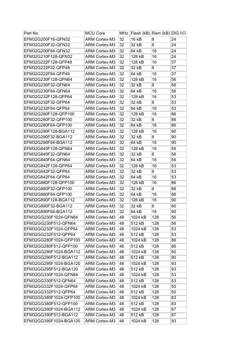
Part No.MCU Core MHz Flash (kB)Ram (kB)DIG I/O EFM32G200F16-QFN32ARM Cortex-M33216 kB824 EFM32G200F32-QFN32ARM Cortex-M33232 kB824 EFM32G200F64-QFN32ARM Cortex-M33264 kB1624 EFM32G210F128-QFN32ARM Cortex-M332128 kB1624 EFM32G222F128-QFP48ARM Cortex-M332128 kB1637 EFM32G222F32-QFP48ARM Cortex-M33232 kB837 EFM32G222F64-QFP48ARM Cortex-M33264 kB1637 EFM32G230F128-QFN64ARM Cortex-M332128 kB1656 EFM32G230F32-QFN64ARM Cortex-M33232 kB856 EFM32G230F64-QFN64ARM Cortex-M33264 kB1656 EFM32G232F128-QFP64ARM Cortex-M332128 kB1653 EFM32G232F32-QFP64ARM Cortex-M33232 kB853 EFM32G232F64-QFP64ARM Cortex-M33264 kB1653 EFM32G280F128-QFP100ARM Cortex-M332128 kB1686 EFM32G280F32-QFP100ARM Cortex-M33232 kB886 EFM32G280F64-QFP100ARM Cortex-M33264 kB1686 EFM32G290F128-BGA112ARM Cortex-M332128 kB1690 EFM32G290F32-BGA112ARM Cortex-M33232 kB890 EFM32G290F64-BGA112ARM Cortex-M33264 kB1690 EFM32G840F128-QFN64ARM Cortex-M332128 kB1656 EFM32G840F32-QFN64ARM Cortex-M33232 kB856 EFM32G840F64-QFN64ARM Cortex-M33264 kB1656 EFM32G842F128-QFP64ARM Cortex-M332128 kB1653 EFM32G842F32-QFP64ARM Cortex-M33232 kB853 EFM32G842F64-QFP64ARM Cortex-M33264 kB1653 EFM32G880F128-QFP100ARM Cortex-M332128 kB1686 EFM32G880F32-QFP100ARM Cortex-M33232 kB886 EFM32G880F64-QFP100ARM Cortex-M33264 kB1686 EFM32G890F128-BGA112ARM Cortex-M332128 kB1690 EFM32G890F32-BGA112ARM Cortex-M33232 kB890 EFM32G890F64-BGA112ARM Cortex-M33264 kB1690 EFM32GG230F1024-QFN64ARM Cortex-M3481024 kB12856 EFM32GG230F512-QFN64ARM Cortex-M348512 kB12856 EFM32GG232F1024-QFP64ARM Cortex-M3481024 kB12853 EFM32GG232F512-QFP64ARM Cortex-M348512 kB12853 EFM32GG280F1024-QFP100ARM Cortex-M3481024 kB12886 EFM32GG280F512-QFP100ARM Cortex-M348512 kB12886 EFM32GG290F1024-BGA112ARM Cortex-M3481024 kB12890 EFM32GG290F512-BGA112ARM Cortex-M348512 kB12890 EFM32GG295F1024-BGA120ARM Cortex-M3481024 kB12893 EFM32GG295F512-BGA120ARM Cortex-M348512 kB12893 EFM32GG330F1024-QFN64ARM Cortex-M3481024 kB12853 EFM32GG330F512-QFN64ARM Cortex-M348512 kB12853 EFM32GG332F1024-QFP64ARM Cortex-M3481024 kB12850 EFM32GG332F512-QFP64ARM Cortex-M348512 kB12850 EFM32GG380F1024-QFP100ARM Cortex-M3481024 kB12883 EFM32GG380F512-QFP100ARM Cortex-M348512 kB12883 EFM32GG390F1024-BGA112ARM Cortex-M3481024 kB12887 EFM32GG390F512-BGA112ARM Cortex-M348512 kB12887 EFM32GG395F1024-BGA120ARM Cortex-M3481024 kB12893EFM32GG840F1024-QFN64ARM Cortex-M3481024 kB12856 EFM32GG840F512-QFN64ARM Cortex-M348512 kB12856 EFM32GG842F1024-QFP64ARM Cortex-M3481024 kB12853 EFM32GG842F512-QFP64ARM Cortex-M348512 kB12853 EFM32GG880F1024-QFP100ARM Cortex-M3481024 kB12886 EFM32GG880F512-QFP100ARM Cortex-M348512 kB12886 EFM32GG890F1024-BGA112ARM Cortex-M3481024 kB12890 EFM32GG890F512-BGA112ARM Cortex-M348512 kB12890 EFM32GG895F1024-BGA120ARM Cortex-M3481024 kB12893 EFM32GG895F512-BGA120ARM Cortex-M348512 kB12893 EFM32GG940F1024-QFN64ARM Cortex-M3481024 kB12853 EFM32GG940F512-QFN64ARM Cortex-M348512 kB12853 EFM32GG942F1024-QFP64ARM Cortex-M3481024 kB12850 EFM32GG942F512-QFP64ARM Cortex-M348512 kB12850 EFM32GG980F1024-QFP100ARM Cortex-M3481024 kB12883 EFM32GG980F512-QFP100ARM Cortex-M348512 kB12883 EFM32GG990F1024-BGA112ARM Cortex-M3481024 kB12887 EFM32GG990F512-BGA112ARM Cortex-M348512 kB12887 EFM32GG995F1024-BGA120ARM Cortex-M3481024 kB12893 EFM32GG995F512-BGA120ARM Cortex-M348512 kB12893 EFM32LG230F128G-E-QFN64ARM Cortex-M348128 kB3256 EFM32LG230F256G-E-QFN64ARM Cortex-M348256 kB3256 EFM32LG230F64G-E-QFN64ARM Cortex-M34864 kB3256 EFM32LG232F128G-E-QFP64ARM Cortex-M348128 kB3253 EFM32LG232F256G-E-QFP64ARM Cortex-M348256 kB3253 EFM32LG232F64G-E-QFP64ARM Cortex-M34864 kB3253 EFM32LG280F128G-E-QFP100ARM Cortex-M348128 kB3286 EFM32LG280F256G-E-QFP100ARM Cortex-M348256 kB3286 EFM32LG280F64G-E-QFP100ARM Cortex-M34864 kB3286 EFM32LG290F128G-E-BGA112ARM Cortex-M348128 kB3290 EFM32LG290F256G-E-BGA112ARM Cortex-M348256 kB3290 EFM32LG290F64G-E-BGA112ARM Cortex-M34864 kB3290 EFM32LG295F128G-E-BGA120ARM Cortex-M348128 kB3293 EFM32LG295F256G-E-BGA120ARM Cortex-M348256 kB3293 EFM32LG295F64G-E-BGA120ARM Cortex-M34864 kB3293 EFM32LG330F128G-E-QFN64ARM Cortex-M348128 kB3253 EFM32LG330F256G-E-QFN64ARM Cortex-M348256 kB3253 EFM32LG330F64G-E-QFN64ARM Cortex-M34864 kB3253 EFM32LG332F128G-E-QFP64ARM Cortex-M348128 kB3250 EFM32LG332F256G-E-QFP64ARM Cortex-M348256 kB3250 EFM32LG332F64G-E-QFP64ARM Cortex-M34864 kB3250 EFM32LG360F128G-E-CSP81ARM Cortex-M348128 kB3265 EFM32LG360F256G-E-CSP81ARM Cortex-M348256 kB3265 EFM32LG360F64G-E-CSP81ARM Cortex-M34864 kB3265 EFM32LG380F128G-E-QFP100ARM Cortex-M348128 kB3283 EFM32LG380F256G-E-QFP100ARM Cortex-M348256 kB3283 EFM32LG380F64G-E-QFP100ARM Cortex-M34864 kB3283 EFM32LG390F128G-E-BGA112ARM Cortex-M348128 kB3287 EFM32LG390F256G-E-BGA112ARM Cortex-M348256 kB3287 EFM32LG390F64G-E-BGA112ARM Cortex-M34864 kB3287EFM32LG395F256G-E-BGA120ARM Cortex-M348256 kB3293 EFM32LG395F64G-E-BGA120ARM Cortex-M34864 kB3293 EFM32LG840F128G-E-QFN64ARM Cortex-M348128 kB3256 EFM32LG840F256G-E-QFN64ARM Cortex-M348256 kB3256 EFM32LG840F64G-E-QFN64ARM Cortex-M34864 kB3256 EFM32LG842F128G-E-QFP64ARM Cortex-M348128 kB3253 EFM32LG842F256G-E-QFP64ARM Cortex-M348256 kB3253 EFM32LG842F64G-E-QFP64ARM Cortex-M34864 kB3253 EFM32LG880F128G-E-QFP100ARM Cortex-M348128 kB3286 EFM32LG880F256G-E-QFP100ARM Cortex-M348256 kB3286 EFM32LG880F64G-E-QFP100ARM Cortex-M34864 kB3286 EFM32LG890F128G-E-BGA112ARM Cortex-M348128 kB3290 EFM32LG890F256G-E-BGA112ARM Cortex-M348256 kB3290 EFM32LG890F64G-E-BGA112ARM Cortex-M34864 kB3290 EFM32LG895F128G-E-BGA120ARM Cortex-M348128 kB3293 EFM32LG895F256G-E-BGA120ARM Cortex-M348256 kB3293 EFM32LG895F64G-E-BGA120ARM Cortex-M34864 kB3293 EFM32LG940F128G-E-QFN64ARM Cortex-M348128 kB3253 EFM32LG940F256G-E-QFN64ARM Cortex-M348256 kB3253 EFM32LG940F64G-E-QFN64ARM Cortex-M34864 kB3253 EFM32LG942F128G-E-QFP64ARM Cortex-M348128 kB3250 EFM32LG942F256G-E-QFP64ARM Cortex-M348256 kB3250 EFM32LG942F64G-E-QFP64ARM Cortex-M34864 kB3250 EFM32LG980F128G-E-QFP100ARM Cortex-M348128 kB3283 EFM32LG980F256G-E-QFP100ARM Cortex-M348256 kB3283 EFM32LG980F64G-E-QFP100ARM Cortex-M34864 kB3283 EFM32LG990F128G-E-BGA112ARM Cortex-M348128 kB3287 EFM32LG990F256G-E-BGA112ARM Cortex-M348256 kB3287 EFM32LG990F64G-E-BGA112ARM Cortex-M34864 kB3287 EFM32LG995F128G-E-BGA120ARM Cortex-M348128 kB3293 EFM32LG995F256G-E-BGA120ARM Cortex-M348256 kB3293 EFM32LG995F64G-E-BGA120ARM Cortex-M34864 kB3293 EFM32TG108F16-QFN24ARM Cortex-M33216 kB417 EFM32TG108F32-QFN24ARM Cortex-M33232 kB417 EFM32TG108F4-QFN24ARM Cortex-M332 4 kB217 EFM32TG108F8-QFN24ARM Cortex-M3328 kB217 EFM32TG110F16-QFN24ARM Cortex-M33216 kB417 EFM32TG110F32-QFN24ARM Cortex-M33232 kB417 EFM32TG110F4-QFN24ARM Cortex-M332 4 kB217 EFM32TG110F8-QFN24ARM Cortex-M3328 kB217 EFM32TG210F16-QFN32ARM Cortex-M33216 kB424 EFM32TG210F32-QFN32ARM Cortex-M33232 kB424 EFM32TG210F8-QFN32ARM Cortex-M3328 kB224 EFM32TG222F16-QFP48ARM Cortex-M33216 kB437 EFM32TG222F32-QFP48ARM Cortex-M33232 kB437 EFM32TG222F8-QFP48ARM Cortex-M3328 kB237 EFM32TG225F16-BGA48ARM Cortex-M33216 kB437 EFM32TG225F32-BGA48ARM Cortex-M33232 kB437 EFM32TG225F8-BGA48ARM Cortex-M3328 kB237 EFM32TG230F16-QFN64ARM Cortex-M33216 kB456EFM32TG230F32-QFN64ARM Cortex-M33232 kB456 EFM32TG230F8-QFN64ARM Cortex-M3328 kB256 EFM32TG232F16-QFP64ARM Cortex-M33216 kB453 EFM32TG232F32-QFP64ARM Cortex-M33232 kB453 EFM32TG232F8-QFP64ARM Cortex-M3328 kB253 EFM32TG822F16-QFP48ARM Cortex-M33216 kB437 EFM32TG822F32-QFP48ARM Cortex-M33232 kB437 EFM32TG822F8-QFP48ARM Cortex-M3328 kB237 EFM32TG825F16-BGA48ARM Cortex-M33216 kB437 EFM32TG825F32-BGA48ARM Cortex-M33232 kB437 EFM32TG825F8-BGA48ARM Cortex-M3328 kB237 EFM32TG840F16-QFN64ARM Cortex-M33216 kB456 EFM32TG840F32-QFN64ARM Cortex-M33232 kB456 EFM32TG840F8-QFN64ARM Cortex-M3328 kB256 EFM32TG842F16-QFP64ARM Cortex-M33216 kB453 EFM32TG842F32-QFP64ARM Cortex-M33232 kB453 EFM32TG842F8-QFP64ARM Cortex-M3328 kB253 EFM32WG230F128-QFN64ARM Cortex-M448128 kB3256 EFM32WG230F256-QFN64ARM Cortex-M448256 kB3256 EFM32WG230F64-QFN64ARM Cortex-M44864 kB3256 EFM32WG232F128-QFP64ARM Cortex-M448128 kB3253 EFM32WG232F256-QFP64ARM Cortex-M448256 kB3253 EFM32WG232F64-QFP64ARM Cortex-M44864 kB3253 EFM32WG280F128-QFP100ARM Cortex-M448128 kB3286 EFM32WG280F256-QFP100ARM Cortex-M448256 kB3286 EFM32WG280F64-QFP100ARM Cortex-M44864 kB3286 EFM32WG290F128-BGA112ARM Cortex-M448128 kB3290 EFM32WG290F256-BGA112ARM Cortex-M448256 kB3290 EFM32WG290F64-BGA112ARM Cortex-M44864 kB3290 EFM32WG295F128-BGA120ARM Cortex-M448128 kB3293 EFM32WG295F256-BGA120ARM Cortex-M448256 kB3293 EFM32WG295F64-BGA120ARM Cortex-M44864 kB3293 EFM32WG330F128-QFN64ARM Cortex-M448128 kB3253 EFM32WG330F256-QFN64ARM Cortex-M448256 kB3253 EFM32WG330F64-QFN64ARM Cortex-M44864 kB3253 EFM32WG332F128-QFP64ARM Cortex-M448128 kB3250 EFM32WG332F256-QFP64ARM Cortex-M448256 kB3250 EFM32WG332F64-QFP64ARM Cortex-M44864 kB3250 EFM32WG360F128G-A-CSP81ARM Cortex-M448128 kB3265 EFM32WG360F256G-A-CSP81ARM Cortex-M448256 kB3265 EFM32WG360F64G-A-CSP81ARM Cortex-M44864 kB3265 EFM32WG380F128-QFP100ARM Cortex-M448128 kB3283 EFM32WG380F256-QFP100ARM Cortex-M448256 kB3283 EFM32WG380F64-QFP100ARM Cortex-M44864 kB3283 EFM32WG390F128-BGA112ARM Cortex-M448128 kB3287 EFM32WG390F256-BGA112ARM Cortex-M448256 kB3287 EFM32WG390F64-BGA112ARM Cortex-M44864 kB3287 EFM32WG395F128-BGA120ARM Cortex-M448128 kB3293 EFM32WG395F256-BGA120ARM Cortex-M448256 kB3293 EFM32WG395F64-BGA120ARM Cortex-M44864 kB3293 EFM32WG840F128-QFN64ARM Cortex-M448128 kB3256EFM32WG840F256-QFN64ARM Cortex-M448256 kB3256 EFM32WG840F64-QFN64ARM Cortex-M44864 kB3256 EFM32WG842F128-QFP64ARM Cortex-M448128 kB3253 EFM32WG842F256-QFP64ARM Cortex-M448256 kB3253 EFM32WG842F64-QFP64ARM Cortex-M44864 kB3253 EFM32WG880F128-QFP100ARM Cortex-M448128 kB3286 EFM32WG880F256-QFP100ARM Cortex-M448256 kB3286 EFM32WG880F64-QFP100ARM Cortex-M44864 kB3286 EFM32WG890F128-BGA112ARM Cortex-M448128 kB3290 EFM32WG890F256-BGA112ARM Cortex-M448256 kB3290 EFM32WG890F64-BGA112ARM Cortex-M44864 kB3290 EFM32WG895F128-BGA120ARM Cortex-M448128 kB3293 EFM32WG895F256-BGA120ARM Cortex-M448256 kB3293 EFM32WG895F64-BGA120ARM Cortex-M44864 kB3293 EFM32WG940F128-QFN64ARM Cortex-M448128 kB3253 EFM32WG940F256-QFN64ARM Cortex-M448256 kB3253 EFM32WG940F64-QFN64ARM Cortex-M44864 kB3253 EFM32WG942F128-QFP64ARM Cortex-M448128 kB3250 EFM32WG942F256-QFP64ARM Cortex-M448256 kB3250 EFM32WG942F64-QFP64ARM Cortex-M44864 kB3250 EFM32WG980F128-QFP100ARM Cortex-M448128 kB3283 EFM32WG980F256-QFP100ARM Cortex-M448256 kB3283 EFM32WG980F64-QFP100ARM Cortex-M44864 kB3283 EFM32WG990F128-BGA112ARM Cortex-M448128 kB3287 EFM32WG990F256-BGA112ARM Cortex-M448256 kB3287 EFM32WG990F64-BGA112ARM Cortex-M44864 kB3287 EFM32WG995F128-BGA120ARM Cortex-M448128 kB3293 EFM32WG995F256-BGA120ARM Cortex-M448256 kB3293 EFM32WG995F64-BGA120ARM Cortex-M44864 kB3293 EFM32ZG108F16-QFN24ARM Cortex-M0+2416 kB417 EFM32ZG108F32-QFN24ARM Cortex-M0+2432 kB417 EFM32ZG108F4-QFN24ARM Cortex-M0+24 4 kB217 EFM32ZG108F8-QFN24ARM Cortex-M0+248 kB217 EFM32ZG110F16-QFN24ARM Cortex-M0+2416 kB417 EFM32ZG110F32-QFN24ARM Cortex-M0+2432 kB417 EFM32ZG110F4-QFN24ARM Cortex-M0+24 4 kB217 EFM32ZG110F8-QFN24ARM Cortex-M0+248 kB217 EFM32ZG210F16-QFN32ARM Cortex-M0+2416 kB424 EFM32ZG210F32-QFN32ARM Cortex-M0+2432 kB424 EFM32ZG210F4-QFN32ARM Cortex-M0+24 4 kB224 EFM32ZG210F8-QFN32ARM Cortex-M0+248 kB224 EFM32ZG222F16-QFP48ARM Cortex-M0+2416 kB437 EFM32ZG222F32-QFP48ARM Cortex-M0+2432 kB437 EFM32ZG222F4-QFP48ARM Cortex-M0+24 4 kB237 EFM32ZG222F8-QFP48ARM Cortex-M0+248 kB237Communications Timers (16-bit)PCAChannelsInternalOscADC 1I2C; SPI; 2 x USART2—±2%12-bit, 4-ch., 1 Msps I2C; SPI; 2 x USART2—±2%12-bit, 4-ch., 1 Msps I2C; SPI; 2 x USART2—±2%12-bit, 4-ch., 1 Msps I2C; SPI; 2 x USART2—±2%12-bit, 4-ch., 1 Msps I2C; SPI; 2 x USART3—±2%12-bit, 4-ch., 1 Msps I2C; SPI; 2 x USART3—±2%12-bit, 4-ch., 1 Msps I2C; SPI; 2 x USART3—±2%12-bit, 4-ch., 1 Msps I2C; SPI; 3 x USART3—±2%12-bit, 8-ch., 1 Msps I2C; SPI; 3 x USART3—±2%12-bit, 8-ch., 1 Msps I2C; SPI; 3 x USART3—±2%12-bit, 8-ch., 1 Msps I2C; SPI; 3 x USART3—±2%12-bit, 8-ch., 1 Msps I2C; SPI; 3 x USART3—±2%12-bit, 8-ch., 1 Msps I2C; SPI; 3 x USART3—±2%12-bit, 8-ch., 1 Msps I2C; SPI; UART; 3 x USART3—±2%12-bit, 8-ch., 1 Msps I2C; SPI; UART; 3 x USART3—±2%12-bit, 8-ch., 1 Msps I2C; SPI; UART; 3 x USART3—±2%12-bit, 8-ch., 1 Msps I2C; SPI; UART; 3 x USART3—±2%12-bit, 8-ch., 1 Msps I2C; SPI; UART; 3 x USART3—±2%12-bit, 8-ch., 1 Msps I2C; SPI; UART; 3 x USART3—±2%12-bit, 8-ch., 1 Msps I2C; SPI; 3 x USART3—±2%12-bit, 8-ch., 1 Msps I2C; SPI; 3 x USART3—±2%12-bit, 8-ch., 1 Msps I2C; SPI; 3 x USART3—±2%12-bit, 8-ch., 1 Msps I2C; 3 x USART3—±2%12-bit, 8-ch., 1 Msps I2C; SPI; 3 x USART3—±2%12-bit, 8-ch., 1 Msps I2C; SPI; 3 x USART3—±2%12-bit, 8-ch., 1 Msps I2C; SPI; UART; 3 x USART3—±2%12-bit, 8-ch., 1 Msps I2C; SPI; UART; 3 x USART3—±2%12-bit, 8-ch., 1 Msps I2C; SPI; UART; 3 x USART3—±2%12-bit, 8-ch., 1 Msps I2C; SPI; UART; 3 x USART3—±2%12-bit, 8-ch., 1 Msps I2C; SPI; UART; 3 x USART3—±2%12-bit, 8-ch., 1 Msps I2C; SPI; UART; 3 x USART3—±2%12-bit, 8-ch., 1 Msps 2 x I2C; I2S; SPI; 3 x USART4—±2%12-bit, 8-ch., 1 Msps 2 x I2C; I2S; SPI; 3 x USART4—±2%12-bit, 8-ch., 1 Msps 2 x I2C; I2S; SPI; 3 x USART4—±2%12-bit, 8-ch., 1 Msps 2 x I2C; I2S; SPI; 3 x USART4—±2%12-bit, 8-ch., 1 Msps 2 x I2C; I2S; SPI; 2 x UART; 3 x USART4—±2%12-bit, 8-ch., 1 Msps 2 x I2C; I2S; SPI; 2 x UART; 3 x USART4—±2%12-bit, 8-ch., 1 Msps 2 x I2C; I2S; SPI; 2 x UART; 3 x USART4—±2%12-bit, 8-ch., 1 Msps 2 x I2C; I2S; SPI; 2 x UART; 3 x USART4—±2%12-bit, 8-ch., 1 Msps 2 x I2C; I2S; SPI; 2 x UART; 3 x USART4—±2%12-bit, 8-ch., 1 Msps 2 x I2C; I2S; SPI; 2 x UART; 3 x USART4—±2%12-bit, 8-ch., 1 Msps 2 x I2C; I2S; SPI; 3 x USART; USB4—±2%12-bit, 8-ch., 1 Msps 2 x I2C; I2S; SPI; 3 x USART; USB4—±2%12-bit, 8-ch., 1 Msps 2 x I2C; I2S; SPI; 3 x USART; USB4—±2%12-bit, 8-ch., 1 Msps 2 x I2C; I2S; SPI; 3 x USART; USB4—±2%12-bit, 8-ch., 1 Msps2 x I2C; I2S; SPI; 2 x UART;3 x USART; USB 4—±2%12-bit, 8-ch., 1 Msps2 x I2C; I2S; SPI; 2 x UART;3 x USART; USB 4—±2%12-bit, 8-ch., 1 Msps2 x I2C; I2S; SPI; 2 x UART;3 x USART; USB 4—±2%12-bit, 8-ch., 1 Msps2 x I2C; I2S; SPI; 2 x UART;3 x USART; USB 4—±2%12-bit, 8-ch., 1 Msps2 x I2C; I2S; SPI; 2 x UART;3 x USART;4—±2%12-bit, 8-ch., 1 MspsUSB2 x I2C; I2S; SPI;3 x USART4—±2%12-bit, 8-ch., 1 Msps 2 x I2C; I2S; SPI; 3 x USART4—±2%12-bit, 8-ch., 1 Msps 2 x I2C; I2S; SPI; 3 x USART4—±2%12-bit, 8-ch., 1 Msps 2 x I2C; I2S; SPI; 3 x USART4—±2%12-bit, 8-ch., 1 Msps 2 x I2C; I2S; SPI; 2 x UART; 3 x USART4—±2%12-bit, 8-ch., 1 Msps 2 x I2C; I2S; SPI; 2 x UART; 3 x USART4—±2%12-bit, 8-ch., 1 Msps 2 x I2C; I2S; SPI; 2 x UART; 3 x USART4—±2%12-bit, 8-ch., 1 Msps 2 x I2C; I2S; SPI; 2 x UART; 3 x USART4—±2%12-bit, 8-ch., 1 Msps 2 x I2C; I2S; SPI; 2 x UART; 3 x USART4—±2%12-bit, 8-ch., 1 Msps 2 x I2C; I2S; SPI; 2 x UART; 3 x USART4—±2%12-bit, 8-ch., 1 Msps 2 x I2C; I2S; SPI; 3 x USART; USB4—±2%12-bit, 8-ch., 1 Msps 2 x I2C; I2S; SPI; 3 x USART; USB4—±2%12-bit, 8-ch., 1 Msps 2 x I2C; I2S; SPI; 3 x USART; USB4—±2%12-bit, 8-ch., 1 Msps 2 x I2C; I2S; SPI; 3 x USART; USB4—±2%12-bit, 8-ch., 1 Msps2 x I2C; I2S; SPI; 2 x UART;3 x USART; USB 4—±2%12-bit, 8-ch., 1 Msps2 x I2C; I2S; SPI; 2 x UART;3 x USART; USB 4—±2%12-bit, 8-ch., 1 Msps2 x I2C; I2S; SPI; 2 x UART;3 x USART; USB 4—±2%12-bit, 8-ch., 1 Msps2 x I2C; I2S; SPI; 2 x UART;3 x USART; USB 4—±2%12-bit, 8-ch., 1 Msps2 x I2C; I2S; SPI; 2 x UART;3 x USART; USB 4—±2%12-bit, 8-ch., 1 Msps2 x I2C; I2S; SPI; 2 x UART;3 x USART; USB 4—±2%12-bit, 8-ch., 1 Msps2 x I2C; I2S; SPI;3 x USART4—±2%12-bit, 8-ch., 1 Msps 2 x I2C; I2S; SPI; 3 x USART4—±2%12-bit, 8-ch., 1 Msps 2 x I2C; I2S; SPI; 3 x USART4—±2%12-bit, 8-ch., 1 Msps 2 x I2C; I2S; SPI; 3 x USART4—±2%12-bit, 8-ch., 1 Msps 2 x I2C; I2S; SPI; 3 x USART4—±2%12-bit, 8-ch., 1 Msps 2 x I2C; I2S; SPI; 3 x USART4—±2%12-bit, 8-ch., 1 Msps 2 x I2C; I2S; SPI; 2 x UART; 3 x USART4—±2%12-bit, 8-ch., 1 Msps 2 x I2C; I2S; SPI; 2 x UART; 3 x USART4—±2%12-bit, 8-ch., 1 Msps 2 x I2C; I2S; SPI; 2 x UART; 3 x USART4—±2%12-bit, 8-ch., 1 Msps 2 x I2C; I2S; SPI; 2 x UART; 3 x USART4—±2%12-bit, 8-ch., 1 Msps 2 x I2C; I2S; SPI; 2 x UART; 3 x USART4—±2%12-bit, 8-ch., 1 Msps 2 x I2C; I2S; SPI; 2 x UART; 3 x USART4—±2%12-bit, 8-ch., 1 Msps 2 x I2C; I2S; SPI; 2 x UART; 3 x USART4—±2%12-bit, 8-ch., 1 Msps 2 x I2C; I2S; SPI; 2 x UART; 3 x USART4—±2%12-bit, 8-ch., 1 Msps 2 x I2C; I2S; SPI; 2 x UART; 3 x USART4—±2%12-bit, 8-ch., 1 Msps 2 x I2C; I2S; SPI; 3 x USART; USB4—±2%12-bit, 8-ch., 1 Msps 2 x I2C; I2S; SPI; 3 x USART; USB4—±2%12-bit, 8-ch., 1 Msps 2 x I2C; I2S; SPI; 3 x USART; USB4—±2%12-bit, 8-ch., 1 Msps 2 x I2C; I2S; SPI; 3 x USART; USB4—±2%12-bit, 8-ch., 1 Msps 2 x I2C; I2S; SPI; 3 x USART; USB4—±2%12-bit, 8-ch., 1 Msps 2 x I2C; I2S; SPI; 3 x USART; USB4—±2%12-bit, 8-ch., 1 Msps2 x I2C; I2S; SPI; 2 x UART;3 x USART; USB 4—±2%12-bit, 8-ch., 1 Msps2 x I2C; I2S; SPI; 2 x UART;3 x USART; USB 4—±2%12-bit, 8-ch., 1 Msps2 x I2C; I2S; SPI; 2 x UART;3 x USART; USB 4—±2%12-bit, 8-ch., 1 Msps2 x I2C; I2S; SPI; 2 x UART;3 x USART; USB 4—±2%12-bit, 8-ch., 1 Msps2 x I2C; I2S; SPI; 2 x UART;3 x USART; USB 4—±2%12-bit, 8-ch., 1 Msps2 x I2C; I2S; SPI; 2 x UART;3 x USART; USB 4—±2%12-bit, 8-ch., 1 Msps2 x I2C; I2S; SPI; 2 x UART;3 x USART; USB 4—±2%12-bit, 8-ch., 1 Msps2 x I2C; I2S; SPI; 2 x UART;3 x USART; USB 4—±2%12-bit, 8-ch., 1 Msps2 x I2C; I2S; SPI; 2 x UART;3 x USART;4—±2%12-bit, 8-ch., 1 MspsUSB2 x I2C; I2S; SPI; 2 x UART;3 x USART; USB 4—±2%12-bit, 8-ch., 1 Msps2 x I2C; I2S; SPI; 2 x UART;3 x USART; USB 4—±2%12-bit, 8-ch., 1 Msps2 x I2C; I2S; SPI;3 x USART4—±2%12-bit, 8-ch., 1 Msps 2 x I2C; I2S; SPI; 3 x USART4—±2%12-bit, 8-ch., 1 Msps 2 x I2C; I2S; SPI; 3 x USART4—±2%12-bit, 8-ch., 1 Msps 2 x I2C; I2S; SPI; 3 x USART4—±2%12-bit, 8-ch., 1 Msps 2 x I2C; I2S; SPI; 3 x USART4—±2%12-bit, 8-ch., 1 Msps 2 x I2C; I2S; SPI; 3 x USART4—±2%12-bit, 8-ch., 1 Msps 2 x I2C; I2S; SPI; 2 x UART; 3 x USART4—±2%12-bit, 8-ch., 1 Msps 2 x I2C; I2S; SPI; 2 x UART; 3 x USART4—±2%12-bit, 8-ch., 1 Msps 2 x I2C; I2S; SPI; 2 x UART; 3 x USART4—±2%12-bit, 8-ch., 1 Msps 2 x I2C; I2S; SPI; 2 x UART; 3 x USART4—±2%12-bit, 8-ch., 1 Msps 2 x I2C; I2S; SPI; 2 x UART; 3 x USART4—±2%12-bit, 8-ch., 1 Msps 2 x I2C; I2S; SPI; 2 x UART; 3 x USART4—±2%12-bit, 8-ch., 1 Msps 2 x I2C; I2S; SPI; 2 x UART; 3 x USART4—±2%12-bit, 8-ch., 1 Msps 2 x I2C; I2S; SPI; 2 x UART; 3 x USART4—±2%12-bit, 8-ch., 1 Msps 2 x I2C; I2S; SPI; 2 x UART; 3 x USART4—±2%12-bit, 8-ch., 1 Msps 2 x I2C; I2S; SPI; 3 x USART; USB4—±2%12-bit, 8-ch., 1 Msps 2 x I2C; I2S; SPI; 3 x USART; USB4—±2%12-bit, 8-ch., 1 Msps 2 x I2C; I2S; SPI; 3 x USART; USB4—±2%12-bit, 8-ch., 1 Msps 2 x I2C; I2S; SPI; 3 x USART; USB4—±2%12-bit, 8-ch., 1 Msps 2 x I2C; I2S; SPI; 3 x USART; USB4—±2%12-bit, 8-ch., 1 Msps 2 x I2C; I2S; SPI; 3 x USART; USB4—±2%12-bit, 8-ch., 1 Msps2 x I2C; I2S; SPI; 2 x UART;3 x USART; USB 4—±2%12-bit, 8-ch., 1 Msps2 x I2C; I2S; SPI; 2 x UART;3 x USART; USB 4—±2%12-bit, 8-ch., 1 Msps2 x I2C; I2S; SPI; 2 x UART;3 x USART; USB 4—±2%12-bit, 8-ch., 1 Msps2 x I2C; I2S; SPI; 2 x UART;3 x USART; USB 4—±2%12-bit, 8-ch., 1 Msps2 x I2C; I2S; SPI; 2 x UART;3 x USART; USB 4—±2%12-bit, 8-ch., 1 Msps2 x I2C; I2S; SPI; 2 x UART;3 x USART; USB 4—±2%12-bit, 8-ch., 1 Msps2 x I2C; I2S; SPI; 2 x UART;3 x USART; USB 4—±2%12-bit, 8-ch., 1 Msps2 x I2C; I2S; SPI; 2 x UART;3 x USART; USB 4—±2%12-bit, 8-ch., 1 Msps2 x I2C; I2S; SPI; 2 x UART;3 x USART; USB 4—±2%12-bit, 8-ch., 1 MspsI2C; I2S; SPI2—±2%—I2C; I2S; SPI2—±2%—I2C; I2S; SPI2—±2%—I2C; I2S; SPI2—±2%—I2C; I2S; SPI; 2 x USART2—±2%12-bit, 2-ch., 1 Msps I2C; I2S; SPI; 2 x USART2—±2%12-bit, 2-ch., 1 Msps I2C; I2S; SPI; 2 x USART2—±2%12-bit, 2-ch., 1 Msps I2C; I2S; SPI; 2 x USART2—±2%12-bit, 2-ch., 1 Msps I2C; I2S; SPI; 2 x USART2—±2%12-bit, 4-ch., 1 Msps I2C; I2S; SPI; 2 x USART2—±2%12-bit, 4-ch., 1 Msps I2C; I2S; SPI; 2 x USART2—±2%12-bit, 4-ch., 1 Msps I2C; I2S; SPI; 2 x USART2—±2%12-bit, 4-ch., 1 Msps I2C; I2S; SPI; 2 x USART2—±2%12-bit, 4-ch., 1 Msps I2C; I2S; SPI; 2 x USART2—±2%12-bit, 4-ch., 1 Msps I2C; I2S; SPI; 2 x USART2—±2%12-bit, 4-ch., 1 Msps I2C; I2S; SPI; 2 x USART2—±2%12-bit, 4-ch., 1 Msps I2C; I2S; SPI; 2 x USART2—±2%12-bit, 4-ch., 1 Msps I2C; I2S; SPI; 2 x USART2—±2%12-bit, 8-ch., 1 MspsI2C; I2S; SPI; 2 x USART2—±2%12-bit, 8-ch., 1 Msps I2C; I2S; SPI; 2 x USART2—±2%12-bit, 8-ch., 1 Msps I2C; I2S; SPI; 2 x USART2—±2%12-bit, 8-ch., 1 Msps I2C; I2S; SPI; 2 x USART2—±2%12-bit, 8-ch., 1 Msps I2C; I2S; SPI; 2 x USART2—±2%12-bit, 4-ch., 1 Msps I2C; I2S; SPI; 2 x USART2—±2%12-bit, 4-ch., 1 Msps I2C; I2S; SPI; 2 x USART2—±2%12-bit, 4-ch., 1 Msps I2C; I2S; SPI; 2 x USART2—±2%12-bit, 4-ch., 1 Msps I2C; I2S; SPI; 2 x USART2—±2%12-bit, 4-ch., 1 Msps I2C; I2S; SPI; 2 x USART2—±2%12-bit, 4-ch., 1 Msps I2C; I2S; SPI; 2 x USART2—±2%12-bit, 8-ch., 1 Msps I2C; I2S; SPI; 2 x USART2—±2%12-bit, 8-ch., 1 Msps I2C; I2S; SPI; 2 x USART2—±2%12-bit, 8-ch., 1 Msps I2C; I2S; SPI; 2 x USART2—±2%12-bit, 8-ch., 1 Msps I2C; I2S; SPI; 2 x USART2—±2%12-bit, 8-ch., 1 Msps I2C; I2S; SPI; 2 x USART2—±2%12-bit, 8-ch., 1 Msps 2 x I2C; I2S; SPI; 3 x USART4—±2%12-bit, 8-ch., 1 Msps 2 x I2C; I2S; SPI; 3 x USART4—±2%12-bit, 8-ch., 1 Msps 2 x I2C; I2S; SPI; 3 x USART4—±2%12-bit, 8-ch., 1 Msps 2 x I2C; I2S; SPI; 3 x USART4—±2%12-bit, 8-ch., 1 Msps 2 x I2C; I2S; SPI; 3 x USART4—±2%12-bit, 8-ch., 1 Msps 2 x I2C; I2S; SPI; 3 x USART4—±2%12-bit, 8-ch., 1 Msps 2 x I2C; I2S; SPI; 2 x UART; 3 x USART4—±2%12-bit, 8-ch., 1 Msps 2 x I2C; I2S; SPI; 2 x UART; 3 x USART4—±2%12-bit, 8-ch., 1 Msps 2 x I2C; I2S; SPI; 2 x UART; 3 x USART4—±2%12-bit, 8-ch., 1 Msps 2 x I2C; I2S; SPI; 2 x UART; 3 x USART4—±2%12-bit, 8-ch., 1 Msps 2 x I2C; I2S; SPI; 2 x UART; 3 x USART4—±2%12-bit, 8-ch., 1 Msps 2 x I2C; I2S; SPI; 2 x UART; 3 x USART4—±2%12-bit, 8-ch., 1 Msps 2 x I2C; I2S; SPI; 2 x UART; 3 x USART4—±2%12-bit, 8-ch., 1 Msps 2 x I2C; I2S; SPI; 2 x UART; 3 x USART4—±2%12-bit, 8-ch., 1 Msps 2 x I2C; I2S; SPI; 2 x UART; 3 x USART4—±2%12-bit, 8-ch., 1 Msps 2 x I2C; I2S; SPI; 3 x USART; USB4—±2%12-bit, 8-ch., 1 Msps 2 x I2C; I2S; SPI; 3 x USART; USB4—±2%12-bit, 8-ch., 1 Msps 2 x I2C; I2S; SPI; 3 x USART; USB4—±2%12-bit, 8-ch., 1 Msps 2 x I2C; I2S; SPI; 3 x USART; USB4—±2%12-bit, 8-ch., 1 Msps 2 x I2C; I2S; SPI; 3 x USART; USB4—±2%12-bit, 8-ch., 1 Msps 2 x I2C; I2S; SPI; 3 x USART; USB4—±2%12-bit, 8-ch., 1 Msps2 x I2C; I2S; SPI; 2 x UART;3 x USART; USB 4—±2%12-bit, 8-ch., 1 Msps2 x I2C; I2S; SPI; 2 x UART;3 x USART; USB 4—±2%12-bit, 8-ch., 1 Msps2 x I2C; I2S; SPI; 2 x UART;3 x USART; USB 4—±2%12-bit, 8-ch., 1 Msps2 x I2C; I2S; SPI; 2 x UART;3 x USART; USB 4—±2%12-bit, 8-ch., 1 Msps2 x I2C; I2S; SPI; 2 x UART;3 x USART; USB 4—±2%12-bit, 8-ch., 1 Msps2 x I2C; I2S; SPI; 2 x UART;3 x USART; USB 4—±2%12-bit, 8-ch., 1 Msps2 x I2C; I2S; SPI; 2 x UART;3 x USART; USB 4—±2%12-bit, 8-ch., 1 Msps2 x I2C; I2S; SPI; 2 x UART;3 x USART; USB 4—±2%12-bit, 8-ch., 1 Msps2 x I2C; I2S; SPI; 2 x UART;3 x USART; USB 4—±2%12-bit, 8-ch., 1 Msps2 x I2C; I2S; SPI; 2 x UART;3 x USART; USB 4—±2%12-bit, 8-ch., 1 Msps2 x I2C; I2S; SPI; 2 x UART;3 x USART; USB 4—±2%12-bit, 8-ch., 1 Msps2 x I2C; I2S; SPI; 2 x UART;3 x USART; USB 4—±2%12-bit, 8-ch., 1 Msps2 x I2C; I2S; SPI;3 x USART4—±2%12-bit, 8-ch., 1 Msps2 x I2C; I2S; SPI;3 x USART4—±2%12-bit, 8-ch., 1 Msps 2 x I2C; I2S; SPI; 3 x USART4—±2%12-bit, 8-ch., 1 Msps 2 x I2C; I2S; SPI; 3 x USART4—±2%12-bit, 8-ch., 1 Msps 2 x I2C; I2S; SPI; 3 x USART4—±2%12-bit, 8-ch., 1 Msps 2 x I2C; I2S; SPI; 2 x UART; 3 x USART4—±2%12-bit, 8-ch., 1 Msps 2 x I2C; I2S; SPI; 2 x UART; 3 x USART4—±2%12-bit, 8-ch., 1 Msps 2 x I2C; I2S; SPI; 2 x UART; 3 x USART4—±2%12-bit, 8-ch., 1 Msps 2 x I2C; I2S; SPI; 2 x UART; 3 x USART4—±2%12-bit, 8-ch., 1 Msps 2 x I2C; I2S; SPI; 2 x UART; 3 x USART4—±2%12-bit, 8-ch., 1 Msps 2 x I2C; I2S; SPI; 2 x UART; 3 x USART4—±2%12-bit, 8-ch., 1 Msps 2 x I2C; I2S; SPI; 2 x UART; 3 x USART4—±2%12-bit, 8-ch., 1 Msps 2 x I2C; I2S; SPI; 2 x UART; 3 x USART4—±2%12-bit, 8-ch., 1 Msps 2 x I2C; I2S; SPI; 2 x UART; 3 x USART4—±2%12-bit, 8-ch., 1 Msps 2 x I2C; I2S; SPI; 3 x USART; USB4—±2%12-bit, 8-ch., 1 Msps 2 x I2C; I2S; SPI; 3 x USART; USB4—±2%12-bit, 8-ch., 1 Msps 2 x I2C; I2S; SPI; 3 x USART; USB4—±2%12-bit, 8-ch., 1 Msps 2 x I2C; I2S; SPI; 3 x USART; USB4—±2%12-bit, 8-ch., 1 Msps 2 x I2C; I2S; SPI; 3 x USART; USB4—±2%12-bit, 8-ch., 1 Msps 2 x I2C; I2S; SPI; 3 x USART; USB4—±2%12-bit, 8-ch., 1 Msps 2 x I2C; I2S; 2 x UART; 3 x USART; USB4—±2%12-bit, 8-ch., 1 Msps2 x I2C; I2S; SPI; 2 x UART;3 x USART; USB 4—±2%12-bit, 8-ch., 1 Msps2 x I2C; I2S; SPI; 2 x UART;3 x USART; USB 4—±2%12-bit, 8-ch., 1 Msps2 x I2C; I2S; SPI; 2 x UART;3 x USART; USB 4—±2%12-bit, 8-ch., 1 Msps2 x I2C; I2S; SPI; 2 x UART;3 x USART; USB 4—±2%12-bit, 8-ch., 1 Msps2 x I2C; I2S; SPI; 2 x UART;3 x USART; USB 4—±2%12-bit, 8-ch., 1 Msps2 x I2C; I2S; SPI; 2 x UART;3 x USART; USB 4—±2%12-bit, 8-ch., 1 Msps2 x I2C; I2S; SPI; 2 x UART;3 x USART; USB 4—±2%12-bit, 8-ch., 1 Msps2 x I2C; I2S; SPI; 2 x UART;3 x USART; USB 4—±2%12-bit, 8-ch., 1 MspsI2C; I2S; SPI2—±2%—I2C; I2S; SPI2—±2%—I2C; I2S; SPI2—±2%—I2C; I2S; SPI2—±2%—I2C; I2S; SPI2—±2%12-bit, 2-ch., 1 Msps I2C; I2S; SPI2—±2%12-bit, 2-ch., 1 Msps I2C; I2S; SPI2—±2%12-bit, 2-ch., 1 Msps I2C; I2S; SPI2—±2%12-bit, 2-ch., 1 Msps I2C; I2S; SPI2—±2%12-bit, 4-ch., 1 Msps I2C; I2S; SPI2—±2%12-bit, 4-ch., 1 Msps I2C; I2S; SPI2—±2%12-bit, 4-ch., 1 Msps I2C; I2S; SPI2—±2%12-bit, 4-ch., 1 Msps I2C; I2S; SPI2—±2%12-bit, 4-ch., 1 Msps I2C; I2S; SPI2—±2%12-bit, 4-ch., 1 Msps I2C; I2S; SPI2—±2%12-bit, 4-ch., 1 Msps I2C; I2S; SPI2—±2%12-bit, 4-ch., 1 MspsADC 2DAC TempSensor DebugInterfaceOther PackageTypePackageSize—12-bit, 1-ch.TRUE SW Low Power; RTC QFN326x6 mm—12-bit, 1-ch.TRUE SW Low Power; RTC QFN326x6 mm—12-bit, 1-ch.TRUE SW Low Power; RTC QFN326x6 mm—12-bit, 1-ch.TRUE SW AES; Low Power; RTC QFN326x6 mm—12-bit, 1-ch.TRUE SW AES; Low Power; RTC QFP487x7 mm—12-bit, 1-ch.TRUE SW AES; Low Power; RTC QFP487x7 mm—12-bit, 1-ch.TRUE SW AES; Low Power; RTC QFP487x7 mm—12-bit, 2ch.TRUE SW AES; Low Power; RTC QFN649x9 mm—12-bit, 2ch.TRUE SW AES; Low Power; RTC QFN649x9 mm—12-bit, 2ch.TRUE SW AES; Low Power; RTC QFN649x9 mm—12-bit, 1-ch.TRUE SW AES; Low Power; RTC QFP6410x10 mm—12-bit, 1-ch.TRUE SW AES; Low Power; RTC QFP6410x10 mm—12-bit, 1-ch.TRUE SW AES; Low Power; RTC QFP6410x10 mm—12-bit, 2ch.TRUE SW AES; Low Power; RTC QFP10014x14 mm—12-bit, 2ch.TRUE SW AES; Low Power; RTC QFP10014x14 mm—12-bit, 2ch.TRUE SW AES; Low Power; RTC QFP10014x14 mm—12-bit, 2ch.TRUE SW AES; Low Power; RTC BGA11210x10 mm—12-bit, 2ch.TRUE SW AES; Low Power; RTC BGA11210x10 mm—12-bit, 2ch.TRUE SW AES; Low Power; RTC BGA11210x10 mm—12-bit, 2ch.TRUE SW AES; LCD; Low Power;RTCQFN649x9 mm—12-bit, 2ch.TRUE SW AES; LCD; Low Power;RTCQFN649x9 mm—12-bit, 2ch.TRUE SW AES; LCD; Low Power;RTCQFN649x9 mm—12-bit, 1-ch.TRUE SW AES; LCD; Low Power;RTCQFP6410x10 mm—12-bit, 1-ch.TRUE SW AES; LCD; Low Power;RTCQFP6410x10 mm—12-bit, 1-ch.TRUE SW AES; LCD; Low Power;RTCQFP6410x10 mm—12-bit, 2ch.TRUE SW AES; LCD; Low Power;RTCQFP10014x14 mm—12-bit, 2ch.TRUE SW AES; LCD; Low Power;RTCQFP10014x14 mm—12-bit, 2ch.TRUE SW AES; LCD; Low Power;RTCQFP10014x14 mm—12-bit, 2ch.TRUE SW AES; LCD; Low Power;RTCBGA11210x10 mm—12-bit, 2ch.TRUE SW AES; LCD; Low Power;RTCBGA11210x10 mm—12-bit, 2ch.TRUE SW AES; LCD; Low Power;RTCBGA11210x10 mm—12-bit, 2ch.TRUE ETM; SW AES; Low Power; RTC QFN649x9 mm—12-bit, 2ch.TRUE ETM; SW AES; Low Power; RTC QFN649x9 mm—12-bit, 2ch.TRUE ETM; SW AES; Low Power; RTC QFP6410x10 mm—12-bit, 2ch.TRUE ETM; SW AES; Low Power; RTC QFP6410x10 mm—12-bit, 2ch.TRUE ETM; SW AES; Low Power; RTC QFP10014x14 mm—12-bit, 2ch.TRUE ETM; SW AES; Low Power; RTC QFP10014x14 mm—12-bit, 2ch.TRUE ETM; SW AES; Low Power; RTC BGA11210x10 mm—12-bit, 2ch.TRUE ETM; SW AES; Low Power; RTC BGA11210x10 mm—12-bit, 2ch.TRUE ETM; SW AES; Low Power; RTC BGA1207x7 mm—12-bit, 2ch.TRUE ETM; SW AES; Low Power; RTC BGA1207x7 mm—12-bit, 2ch.TRUE ETM; SW AES; Low Power; RTC QFN649x9 mm—12-bit, 2ch.TRUE ETM; SW AES; Low Power; RTC QFN649x9 mm—12-bit, 2ch.TRUE ETM; SW AES; Low Power; RTC QFP6410x10 mm—12-bit, 2ch.TRUE ETM; SW AES; Low Power; RTC QFP6410x10 mm—12-bit, 2ch.TRUE ETM; SW AES; Low Power; RTC QFP10014x14 mm—12-bit, 2ch.TRUE ETM; SW AES; Low Power; RTC QFP10014x14 mm—12-bit, 2ch.TRUE ETM; SW AES; Low Power; RTC BGA11210x10 mm—12-bit, 2ch.TRUE ETM; SW AES; Low Power; RTC BGA11210x10 mm—12-bit, 2TRUE ETM; SW AES; Low Power; RTC BGA1207x7 mm。
EFM32外设模块—ACMP V1.00

目录1. 概述 (1)2. FAQ (3)2.1 ACMP输入通道 (3)2.2 ACMP中断 (3)2.3 电容感应模式 (4)3. 实验指导 (6)3.1 实验目的 (6)3.2 实验设备 (6)3.3 实验内容 (6)3.4 试验步骤 (6)3.5 实验参考程序 (6)3.6 实验结果 (8)4. 免责声明 (9)1. 概述模拟比较器(Analog Comparator,简称ACMP)是EFM32系列微控制器片上模拟电压比较模块,可工作于EM0~EM3模式,支持偏置电流、响应时间和滞回电压等配置。
ACMP用来比较两个模拟输入通道的输入电压大小并输出高低电平指示两个输入电压高低情况。
EFM32系列微控制器片上模拟比较器可选的输入信号包括内部参考电压、DAC 输出和外部输入引脚等,其输出信号可以输出到GPIO或PRS。
模拟比较器也可配置为电容感应模式以用来开发电容传感器类应用。
通过改变模拟比较器的偏置电流,可以改变其响应时间和功耗。
模拟比较器的内部参考电压可工作在正常模式和低功耗模式。
如图1.1所示为模拟比较器内部的互连情况、内部参考电压和输出模式的选择等。
图1.1 模拟比较器结构框图注:Gecko系列芯片ACMP的输入不含DAC通道0和DAC通道1。
模拟比较器有两个模拟输入端,即同相输入端和反相输入端。
当模拟比较器开始工作时,输出信号指示两输入通道电压的高低情况。
当同相输入电压高于反相输入电压时,模拟比较器输出高电平,反之输出低电平。
8路外部输入通道均可配置为同相输入或反相输入,但内部参考源和DAC输入通道(对于Gecko 系列没有DAC 通道0和1)只能配置为反相输入。
内部参考源包括1.25V 带隙基准电压、2.5V 带隙基准电压和VDD 参考源,其中VDD 参考源的输出电压可以通过配置ACMPn_INPUTSEL 寄存器中VDDLEVEL 位进行改变,分压公式如下:63/VDDLEVEL V V DD SCALED _DD ×=模拟比较器的输出可以从ACMPn_STATUS 寄存器中的ACMPOUT 位读出。
Silicon Labs携手Edge Impulse加速实现机器学习应用

敬请登录网站在线投稿(t o u ga o .m e s n e t .c o m.c n )2021年第4期29方法也有所不同㊂例如本文中所举的两个实例,如果运行在已经定制好内核的O K 2410终端板,是不需要进行界面再调试的,P C 端的程序直接下载即可㊂此时,H 模型只需要完成上半部分㊂在嵌入式开发中,还可以采取介于基于控件和基于绘图之间的做法,即把控件随意拖拽至窗体上,而后通过代码调整彼此之间的相对位置,完成界面的初步实现,其后的调试仍旧可按照H 模型的方法来完成㊂经过实践,说明H 模型方法具有较好的实用性和可操作性㊂但是,随着界面复杂性的提高,对于H 模型的适应要求则更高,需要对其进行更深入的研究与探索㊂参考文献[1]张银奎.软件调试[M ].北京:电子工业出版社,2008.[2]S P S r e e j a ,N a v e e n K u m a r S ,M a n o h a r R .A R e v i e w o n S o f t w a r e T e s i n g M e t h o d o l o gi e s [J ].I n t e r n a t i o n a l J o u r n a l o f R e c e n t T r e n d s i n E n g i n e e r i n g &R e s e a r c h ,2018,4(3):229234.[3]J o h n R o b b i n s .应用程序调试技术[M ].潘文林,等译.北京:清华大学出版社,2001.[4]V a h i d G a r o u s i ,M i c h a e l F e l d e r e r .W h a t w e k n o w a b o u t t e s -t i n g e m b e d d e d s o f t w a r e [J ].I E E E S o f t w a r e ,2018,35(4):6269.[5]蔡建平.嵌入式软件测试实用技术[M ].北京:清华大学出版社,2010.[6]J K R S a s t r y ,M L a k s h m i P r a s a d .T e s t i n g e m b e d d e d s ys t e m t h r o u g h o p t i m a l m i n i n g t e c h n i qu e (OMT )b a s e d o n m u l t i i n pu t d o m a i n [J ].I n t e r n a t i o n a l J o u r a n a l o f E l e c t r i c a l a n d C o m p u t e r E n g i i n e e r i n g,2019,9(3):21412151.[7]张光兰,万莹.移动应用G U I 测试技术综述[J ].现代计算机,2019(10):4448.[8]I s a b e l l a ,E m i R e t n a .S t u d y P a pe r o n T e s t C a s e g e n e r a t i o nf o r G U I B a s e d T e s t i ng [J ].I n t e r n a t i o n a l J o u r n a l o f S o f t w a r e E n g i n e e r i n g &A p pl i c a t i o n s ,2012,3(1):139147.[9]吴建湘.基于嵌入式L i n u x 系统下的Q t 测试软件开发[J ].电脑迷,2018(11):59.[10]沈炜,王晓聪.基于Q t 的嵌入式图形界面的研究与应用[J ].工业控制计算机,2016,29(1):101102,104.[11]戴莉萍.基于Q t 与A n d r o i d 的实验查错系统设计与实现[J ].实验室研究与探索,2017(1):132135.[12]龚丽.浅谈Q t 中的布局管理[J ].电脑知识与技术(学术交流),2014(9):58835886.[13]R i m a n t a s S e i n a u s k a s ,V yt e n i s S e i n a u s k a s .E x a m i n a t i o n o f t h e p o s s i b i l i t i e s f o r i n t e g r a t e d t e s t i n g o f e m b e d d e d s ys t e m s [J ].A m e r i c a n J o u r n a l o f E m b e d d e d S y s t e m s a n d A p pl i c a -t i o n s ,2013,1(1):112.[14]M a t t T e l l e r s ,Y u a n H s i e h .程序调试思想与实践[M ].邓劲生,等译.北京:中国水利水电出版社,2002.[15]G l e n f o r d J M ye r s .软件测试的艺术[M ].王峰,等译.北京:机械工业出版社,2006.[16]安晓辉.Q t o n A n d r o i d 核心编程[M ].北京:电子工业出版社,2014.戴莉萍(讲师),主要研究方向为软件工程㊂(责任编辑:薛士然 收稿日期:2020-10-10)S i l i c o n L a b s 携手E d g e I m pu l s e 加速实现机器学习应用S i l i c o n L a b s (亦称 芯科科技 )宣布与领先的边缘设备机器学习(M L )开发平台E d g e I m pu l s e 携手合作,实现在S i l i c o n L a b s E F R 32无线片上系统(S o C )和E F M 32微控制器(M C U )上快速开发和部署机器学习应用㊂E d g e I m pu l s e 工具可在低功耗且内存受限的远程边缘设备上实现复杂的运动检测(m o t i o n d e t e c t i o n)㊁声音识别和图像分类㊂研究表明,往往由于人工智能(A I )/机器学习方面的挑战,87%的数据科学项目从未实现量产㊂通过S i l i c o n L a b s 与E d ge I m -p u l s e 之间的这种新合作,设备开发人员只需轻点按钮,即可直接生成机器学习模型并将其导出至设备或S i m p l i c i t y St u d i o (S i l i c o n L a b s 的集成开发环境),在数分钟内便可实现机器学习功能㊂S i l i c o n L a b s 物联网副总裁M a t t S a u n d e r s 表示: S i l i c o n L a b s 相信,我们努力将机器学习融入到边缘设备中,将会使物联网更加智能㊂E d g e I m p u l s e 提供安全㊁私密且容易使用的工具,在实现机器学习时为开发人员节省了时间和资金,并为从预测性维护㊁资产跟踪到监控和人员检测等实际商业应用带来了令人惊叹的新用户体验㊂通过在S i m p l i c i t y S t u d i o 中集成部署,E d g e I m pu l s e 可使开发人员免费在各种S i l i c o n L a b s 产品上快速创建神经网络㊂通过在E F R 32和E F M 32器件(例如MG 12㊁MG 21和G G 11)中嵌入最先进的T i n yM L 模型,该解决方案能够实现以下功能:真实的传感器数据收集和存储㊁高级信号处理和数据特征提取㊁机器学习㊁深度神经网络(D N N )模型训练㊁优化嵌入式代码部署㊂E d ge I m -p u l s e 工具还可以利用E d g e I m p u l s e 的E d g e O pt i m i z e d N e u r a l (E O N )技术来优化内存使用和推理时间㊂E d g e I m p u l s e 联合创始人兼首席执行官Z a c h S h e l b y 表示:嵌入式机器学习在工业㊁企业和消费领域的应用是无止境的㊂将机器学习与S i l i c o n L a b s 的先进开发工具和多协议解决方案整合在一起,将为客户带来绝佳的无线开发机遇㊂。
WF200 Wi-Fi Expansion Kit用户手册说明书
UG379: WF200 Wi-Fi® Expansion Kit User's GuideThe WF200 Wi-Fi Expansion Kit is an excellent way to explore and evaluate the WF200 Wi-Fi® Transceiver with a Raspberry Pi or an EFM32 MCU for your embedded application.The WF200 Wi-Fi® Transceiver is an easy to use and easy to interface Wi-Fi Network Co-Processor (NCP). Most of the associated complexity of Wi-Fi and the protocol stack is offloaded to the NCP and allows for easy Wi-Fi integration into any embedded sys-tem.The kit easily integrates and brings Wi-Fi connectivity to a compatible Silicon Labs MCU Starter Kit through the EXP header. The WF200 Wi-Fi Expansion Kit has also been designed after the Raspberry Pi Hardware Attached on Top (HAT) board specifi-cation, allowing the WF200 Wi-Fi Expansion Kit to connect to a Raspberry Pi.WF200 EXPANSION BOARD FEATURES•EXP connector for interfacing Silicon Labs Starter Kits•Selectable SPI or SDIO host interface •Allows board detection and identification•Raspberry Pi compatible HAT •40-pin header •HAT EEPROM for identificationTable of Contents1. Introduction (3)2. Hardware Overview (5)2.1 Hardware Layout (5)3. WF200 Wi-Fi NCP Expansion Kit (6)3.1 Host Interfaces (6)3.2 Power-on and Manual Reset Circuit (7)4. Connectors (8)4.1 EXP Header (9)4.1.1 Pass-through EXP Header (9)4.1.2 EXP Header Pinout (10)4.2 Raspberry Pi Connector (11)4.2.1 Raspberry Pi Connector Pinout (12)4.3 External FEM Connector (13)4.3.1 External FEM Connector Pinout (13)4.4 PTA Connector (14)4.4.1 PTA Connector Pinout (14)4.5 Secondary RF Connector (14)4.6 Power Supply (15)5. Schematics, Assembly Drawings, and BOM (16)6. Kit Revision History (17)6.1 SLEXP8022A Revision History (17)6.2 SLEXP8022B Revision History (17)7. Document Revision History (18)1. IntroductionThis user guide covers the WF200 Wi-Fi Expansion Kit. The kit connects to either a Silicon Labs EFM32 MCU starter kit (STK), a Sili-con Labs EFR32 wireless starter kit (WSTK) or a Raspberry Pi equipped with the 40-pin Raspberry Pi hardware-attached-on-top (HAT) connector. SDIO support is available only with selected hosts.The pictures below shows the kit connected to a Silicon Labs MCU STK through the Expansion Header and a Raspberry Pi 3, respec-tively.Figure 1.1. WF200 Wi-Fi Expansion Kit Connected to a Silicon Labs EFM32GG11 MCU STKNote: Do not connect the kit to both a Silicon Labs MCU STK and a Raspberry Pi at the same time.2. Hardware Overview2.1 Hardware LayoutThe layout of the WF200 Wi-Fi Expansion Kit is shown in the figure below.EXP-header for Starter Kits Power source select switchPass-through EXP-header Not mountedWF200 Wi-Fi TransceiverRaspberry Pi connectorOn bottom sideCurrent consumptionmeasurement headerNot mountedWF200 Wi-FiExpansion BoardHost interfaceselect switchSecondary RF outputcoaxial connectorTX/RX Activity LEDExternal FEM headerNot mountedPTA headerNot mountedReset buttonFigure 2.1. WF200 Wi-Fi Expansion Kit Hardware LayoutHardware Overview3. WF200 Wi-Fi NCP Expansion KitThe WF200 Wi-Fi® Transceiver is a Wi-Fi Network Co-Processor (NCP) transceiver from Silicon Labs.3.1 Host InterfacesThere are two available host interfaces (HIF) on the WF200 Wi-Fi Expansion Kit: SPI or SDIO. Which interface to use is selected using a slide switch, whose state is sampled during power-on reset or manually issued reset. The slide switch must remain in the same posi-tion throughout the duration of the session since it also controls HIF selection multiplexer circuits.When the WF200 Wi-Fi Expansion Kit is connected to an EFM32/EFR32 starter kit through the EXP header, the state of the HIF selec-tion switch can be read (but not controlled) by the kit mcu through a GPIO pin.The WF200 Wi-Fi Expansion Kit incorporates a set of multiplexer circuits which allows the user to use the same kit for evaluating the WF200 in both applications requiring SPI or SDIO connectivity to the host. These circuits will normally not be needed in an end-user application since in most cases the interface to use will be fixed.A simplified circuit diagram showing the host interface multiplexer circuits is shown below. The EXP_HEADER9 signal is connected to pin 9 on the EXP header, while the HIF_OEn output enable signal is controlled by the power-on reset circuit (explained later).Figure 3.1. Host Interface Multiplexer Circuit3.2 Power-on and Manual Reset CircuitTo ensure that the state of the host interface selection signal to be sampled correctly at the rising edge of the WF200 RESETn signal, a power-on reset circuit has been added to the WF200 Wi-Fi Expansion Kit. This circuit achieves this by•Adding a delay of 1ms to the rising edge of the RESETn signal compared to the rising edge of the power supply•Isolating the host from the WF200 DAT2/HIF_SEL pin during the rising edge of the RESETn signalThe figure below shows the circuit diagram for the power-on and manual reset circuit. Its functionality is as follows:•NCP_RESETn is the active-low reset signal of the WF200. The WF200 RESETn pin has an internal pull-up of approx. 70 kOhms.The on-board reset button is connected to this signal.•HIF_SEL_CTRL is the signal from the HIF selection switch•HIF_OEn is the active-low output enable signal of the HIF multiplexer circuits•WF200_DAT2_HIF_SEL is the combined SDIO DAT2 signal and HIF selection signal of the WF200•U114 is an open-drain active low output reset monitor which with the installed capacitor connected to the CD pin keeps NCP_RE-SETn tied to ground for about 1 ms after VMCU_NCP has exceeded the threshold voltage of 0.9 volts•U115 is a tri-state output buffer with an active low output enable signal connected to NCP_RESETn which pulls the CD pin of U116 low while NCP_RESETn is low•U116 is a push-pull active high output reset monitor which drives HIF_OEn high for 1 ms after the output of U115 is disabled•U109 is a tri-state output buffer with an active high output enable signal which connects the HIF_SEL_CTRL signal to the WF200_DAT2_HIF_SEL signal as long as HIF_OEn is highThe NCP_RESETn signal is available on both the EXP header and the Raspberry Pi connector and can be used for issuing a manual reset sequence by pulling it low for at least 1 ms.Figure 3.2. Power-on and Manual Reset Circuit Diagram4. ConnectorsThis chapter gives an overview of the WF200 Wi-Fi Expansion Kit connectivity and power connections.Pass-through EXP Header(Bottom side)External FEM connector Figure 4.1. WF200 Wi-Fi Expansion Kit Connector Layout4.1 EXP HeaderOn the left-hand side of the WF200 Wi-Fi Expansion Kit, a right-angle female 20-pin EXP header is provided to allow connection to one of Silicon Labs’ supported Starter Kits. The EXP header on the Starter Kits follows a standard which ensures that commonly used pe-ripherals such as an SPI, a UART, and an I2C bus, are available on fixed locations on the connector. Additionally, the VMCU, 3V3 and 5V power rails are also available on the expansion header. For detailed information regarding the pinout to the expansion header on a specific Starter Kit, consult the accompanying user’s guide.The figure below shows how the WF200 Wi-Fi® Transceiver is connected to the connector and the peripheral functions that are availa-ble.VMCUSPI_MOSI / SDIO_DAT1SPI_MISO / SDIO_DAT0SPI_SCLK / SDIO_CMD SPI_CS / SDIO_CLK SPI_WIRQ / SDIO_DAT3SDIO_DAT2Not Connected (NC)5V3V3GNDGPIO_WUP Not Connected (NC)RESETnHIF_SEL_CTRL Not Connected (NC)Not Connected (NC)Not Connected (NC)BOARD_ID_SDA BOARD_ID_SCL Reserved (Board Identification)WF200 I/O PinFigure 4.2. Expansion Header4.1.1 Pass-through EXP HeaderThe WF200 Wi-Fi Expansion Kit features a footprint for a secondary EXP header. All signals from the EXP header, including those that are not connected to any features on the WF200 Wi-Fi Expansion Kit, are directly tied to the corresponding pins in the footprint, allow-ing daisy-chaining of additional expansion boards if a connector is soldered in.4.1.2 EXP Header PinoutThe table below shows the pin assignments of the EXP header.Table 4.1. EXP Header Pinout4.2 Raspberry Pi ConnectorOn the bottom side of the WF200 Wi-Fi Expansion Kit, a dual row, female socket, 0.1" pitch connector is soldered in to allow the WF200Wi-Fi Expansion Kit to act as a Raspberry Pi Hardware Attached on Top (HAT) board.The figure below shows how the WF200 Wi-Fi® Transceiver is connected to the connector and the peripheral functions that are availa-ble.Reserved (Board Identification)WF200 I/O PinGNDSDIO_DAT2Not Connected (NC)RESETnGPIO_WIRQNot Connected (NC)RPI_ID_SDGND SPI_SCLKSPI_MISO Not Connected (NC)Not Connected (NC)SPI_WIRQGNDGPIO_WUP GNDRPI_ID_SC Not Connected (NC)SDIO_DAT1SPI_CSSPI_MOSI 3V3SDIO_CLKSDIO_DAT3 Not Connected (NC)GNDNot Connected (NC)Not Connected (NC) Not Connected (NC)3V3GNDSDIO_DAT0SDIO_CMD GNDNot Connected (NC)GPIO_FEM_5GPIO_FEM_6GND5V 5VFigure 4.3. Raspberry Pi Connector4.2.1 Raspberry Pi Connector PinoutThe table below shows the pin assignments of the Raspberry Pi connector, and the port pins and peripheral functions that are available on the WF200 Wi-Fi Expansion Kit.Table 4.2. Raspberry Pi Connector Pinout4.3 External FEM ConnectorThe WF200 Wi-Fi Expansion Kit features a 2x5-pin 0.1" pitch connector exposing the WF200 Wi-Fi® Transceiver's external front-end module (FEM) interface, which allows the connection of an external FEM board using a ribbon cable.The WF200 Wi-Fi Expansion Kit also features a TX/RX Activity indicator LED which is connected to the FEM_5 signal.The pinout of the connector is illustrated in the figure below.GNDFEM_PDETFEM_6FEM_5VMCU_NCPFEM_4FEM_3VMCU_NCPFEM_2FEM_1Figure 4.4. External FEM Connector4.3.1 External FEM Connector PinoutThe pin assignment of the external FEM connector on the board is given in the table below.Table 4.3. External FEM Connector Pin Descriptions4.4 PTA ConnectorThe WF200's packet transfer arbitration (PTA) interface for managing coexistence in a multi-transceiver application is exposed on a 1x5-pin 0.1" pitch header on the WF200 Wi-Fi Expansion Kit.The pinout of the connector is illustrated in the figure below.PTA_STATUS / PRIORITY PTA_RF_ACT / REQUESTPTA_FREQ / RHOPTA_TX_CONF / GRANT GNDFigure 4.5. PTA Connector4.4.1 PTA Connector PinoutThe pin assignment of the PTA connector on the board is given in the table below.Table 4.4. PTA Connector Pin Descriptions4.5 Secondary RF ConnectorThe WF200's secondary RF output is exposed on the WF200 Wi-Fi Expansion Kit through a Hirose u.FL coaxial connector. Matching components on the board ensure that a 50 ohm characteristic impedance is seen when connecting an external antenna or RF meas-urement equipment to this connector.For connecting the secondary RF output to an RF measurement instrument, a u.FL to SMA adapter cable (not included with the kit) can be used. Examples of such adapter cables are the Taoglas CAB.721 (100 mm) or CAB.720 (200 mm) cable assemblies.4.6 Power SupplyThere are two ways to provide power to the kit:•The kit can be connected to, and powered by, a Silicon Labs MCU STK •The kit can be connected to, and powered by, a Raspberry PiNote: Connecting the WF200 Wi-Fi Expansion Kit to both an EFM32/EFR32 STK and a Raspberry Pi at the same time is not a valid option.When connected to a Silicon Labs MCU STK, the WF200 Wi-Fi® Transceiver can either be powered by the VMCU rail present on the EXP header or through an LDO regulator on board the WF200 Wi-Fi Expansion Kit. If connected to the VMCU rail of the starter kit, the current consumption of the WF200 Wi-Fi® Transceiver will be included in the starter kit's on-board Advanced Energy Monitor (AEM)measurements. The LDO regulator draws power from the 5V net, and, hence, the power consumption of the WF200 Wi-Fi® Transceiv-er will not be included in any AEM measurements performed by the MCU STK.A mechanical power switch on the WF200 Wi-Fi Expansion Kit is used to select between Low Power (AEM) mode and High Power (LDO) mode. When the switch is set to Low Power (AEM) mode, the WF200 Wi-Fi® Transceiver is connected to the VMCU net on the Expansion Header. When the switch is set to High Power (LDO) mode, the WF200 Wi-Fi® Transceiver is connected to the output of the LDO. For applications requiring high power consumption or when the WF200 Wi-Fi Expansion Kit is connected to a Raspberry Pi, the power switch must be set to High Power (LDO) mode.A 0.1 ohm current sense resistor accompanied by a 2x2-pin 0.1" unpopulated header is provided in order to measure the current con-sumption of the WF200 Wi-Fi® Transceiver in situations where AEM is not available or when the current consumption exceeds the measurement range of AEM.The power topology is illustrated in the figure below.Expansion HeaderRaspberry Pi ConnectorFigure 4.6. WF200 Wi-Fi Expansion Kit Power TopologySchematics, Assembly Drawings, and BOM 5. Schematics, Assembly Drawings, and BOMSchematics, assembly drawings, and bill of materials (BOM) are available through Simplicity Studio when the kit documentation pack-age has been installed. They are also available from the Silicon Labs website and kit page.6. Kit Revision HistoryThe kit revision can be found printed on the kit packaging label, as outlined in the figure below.SLEXP8022A WF200 WiFi Expansion Kit19020204219-01-08A00Figure 6.1. Kit Label6.1 SLEXP8022A Revision History6.2 SLEXP8022B Revision History Kit Revision HistoryDocument Revision History 7. Document Revision HistoryRevision 1.02019-01-08•Initial document revision.Silicon Laboratories Inc.400 West Cesar Chavez Austin, TX 78701USASimplicity StudioOne-click access to MCU and wireless tools, documentation, software, source code libraries & more. Available for Windows, Mac and Linux!IoT Portfolio /IoTSW/HW/simplicityQuality /qualitySupport and CommunityDisclaimerSilicon Labs intends to provide customers with the latest, accurate, and in-depth documentation of all peripherals and modules available for system and software implementers using or intending to use the Silicon Labs products. Characterization data, available modules and peripherals, memory sizes and memory addresses refer to each specific device, and "Typical" parameters provided can and do vary in different applications. Application examples described herein are for illustrative purposes only. Silicon Labs reserves the right to make changes without further notice and limitation to product information, specifications, and descriptions herein, and does not give warranties as to the accuracy or completeness of the included information. Silicon Labs shall have no liability for the consequences of use of the information supplied herein. This document does not imply or express copyright licenses granted hereunder to design or fabricate any integrated circuits. The products are not designed or authorized to be used within any Life Support System without the specific written consent of Silicon Labs. A "Life Support System" is any product or system intended to support or sustain life and/or health, which, if it fails, can be reasonably expected to result in significant personal injury or death. Silicon Labs products are not designed or authorized for military applications. Silicon Labs products shall under no circumstances be used in weapons of mass destruction including (but not limited to) nuclear, biological or chemical weapons, or missiles capable of delivering such weapons.Trademark InformationSilicon Laboratories Inc.® , Silicon Laboratories®, Silicon Labs®, SiLabs® and the Silicon Labs logo®, Bluegiga®, Bluegiga Logo®, Clockbuilder®, CMEMS®, DSPLL®, EFM®, EFM32®, EFR, Ember®, Energy Micro, Energy Micro logo and combinations thereof, "the world’s most energy friendly microcontrollers", Ember®, EZLink®, EZRadio®, EZRadioPRO®, Gecko®, ISOmodem®, Micrium, Precision32®, ProSLIC®, Simplicity Studio®, SiPHY®, Telegesis, the Telegesis Logo®, USBXpress®, Zentri and others are trademarks or registered trademarks of Silicon Labs. ARM, CORTEX, Cortex-M3 and THUMB are trademarks or registered trademarks of ARM Holdings. Keil is a registered trademark of ARM Limited. All other products or brand names mentioned herein are trademarks of their respective holders.。
EFM32中文资料(Wurth Electronics)中文数据手册「EasyDatasheet - 矽搜」

n 调试与SEGGERJ-Link调试器 n 能源调试,集成先进能源监控(AEM)
和电压监控
我们更多最小电感:
n WE-TPC SMD屏蔽微型功率电感器 (尺寸2811,2813,2828和3510)
n WE-EHPI能量收集功率电感器 n WE-PMI功率多层电感器
n 设置适当跳线JP1到JP4
喂收获源到功率 连接器
n 可选设置跳线JP9为ON
扩展缓存容量为所有 收割机或
设置跳线JP10为ON延长 缓存容量为TEG收割机
n 您应用程序连接到电源 连接器
警告: n 只有一个源选择必须被设置
在一个时间 n 只有一个缓冲盖选择必须被设置
为ON时间
Solar
热
太阳能电池
LTC3588 - 感应式能量收集
电源
磁性
n WERI连接器
伍尔特Elektronik公司提供更完整解决方案 ,如样品套 件连续免费重新填充,EMC实验室支持,研讨会,技术设
计书以及更多!
能量收集 解决方案为去
Energy Micro’sEFM32 Giant Gecko Starter Kit Linear Technology Multi-Source Energy Harvester Highest efficient passive components
芯片中文手册,看全文,戳
该EFM32GG-STK3700提供 n 评估世界上最节能微控制器EFM32 Gecko家
庭
- 在电路板:EFM32GG990F1024用ARMCortexM3,48兆赫,1024 KB闪存, 128 KB RAM,LCD控制器,USB,低能量感,备用电源域等.
efm32的初步了解和学习
efm32的初步了解和学习
具体怎么找资料。
1. 直接官⽹搜你的芯⽚。
⽐如我efm32gg380f512
2. 找到对应的⼿册资料,⽐如芯⽚的芯⽚⼿册,相关寄存器的资料等等。
还有参考代码
使⽤官⽅的ide下载资料 simpicity studio
下这个的⽬的,⼀般使⽤库函数,相关外设不知道,程序代码该怎么写。
之后就是学习了。
#define GPIOA ((GPIO_TypeDef*)GPIOA_BASE)
1)GPIOA_BASE被强制转换为地址,空间以GPIO_TypeDef的类型进⾏构建,⾸址为GPIOA_BASE,空间内有成员,之间依各⾃固有类型顺序分配相应空间;
2)GPIOA宏展开,即为紧跟其后的具体内容,这样它就是⼀个指针了:指向以GPIOA_BASE为⾸址的结构体空间。
所以您给出GPIOA->某成员,则操作成⽴,如取该成员地址、赋值等。
EFR32 系列1 布局设计指南说明书
AN928.1:EFR32 布局设计指南本应用说明旨在帮助用户利用能够实现优良 RF 性能的设计实践,设计 EFR32 无线 Gecko 产品组合的 PCB。
2.4 GHz 匹配原则载于应用说明AN930.1:EFR32 系列 1 2.4 GHz 匹配指南,1 GHz 以下部分的匹配流程在AN923:EFR32 1 GHz 以下匹配指南中讨论。
以下应用说明详细介绍了与 MCU 相关的主题:AN0918.1:MCU 系列 0 至 EFM32GG1x/TG11 兼容性和迁移指南,AN0948:电源配置和 DC-DC以及AN0955:CRYPTO。
Silicon Labs MCU 和无线入门套件以及 Simplicity Studio 提供强大的开发和调试环境。
为利用自定义硬件的功能和特性,Silicon Labs 推荐在自定义硬件设计中包含调试和编程接口连接器。
有关包含这些连接器接口的详细信息和优点在AN958:自定义设计的调试和编程接口中有详细阐述。
EFR32 内部直流转换器的电源配置和合理用法载于AN0948:电源配置和 DC-DC。
RF 性能很大程度上依赖于 PCB 布局以及匹配网络的设计。
为实现最佳性能,Silicon Labs 建议使用下列部分所述的 PCB 布局设计指南。
内容要点•提供参考示意图和 PCB 布局•列出并描述所有主要设计原则•提供所有设计原则的摘要对照表1.使用 EFR32 系列 1 无线 MCU 的设计建议•已使用 Silicon Labs 提供的参考设计完成广泛测试。
建议设计者按原样使用参考设计,因为其能够尽可能减小寄生现象导致或不良元件布置和 PCB 排线产生的失谐作用。
EFR32 参考设计文件位于 Simplicity Studio 的“套件文档”选项卡下。
•设计的紧凑型 RF 部分(不包括 50 Ω 单端天线)以蓝框圈出,强烈建议使用圈出的 RF 布局,以避免出现任何可能的失谐作用。
一种穿戴式心肺监测系统的设计及其试验研究

一种穿戴式心肺监测系统的设计及其试验研究帅万钧;赵淑丽;李文喆;高华永;蒋建;陈曦;杨金花;晁勇;曹征涛【期刊名称】《医疗卫生装备》【年(卷),期】2024(45)4【摘要】目的:设计一种穿戴式心肺监测系统,并通过人体初步试验验证该系统的性能。
方法:该系统由数据采集器、穿戴胸衣以及信息管理平台组成。
其中,数据采集器以EFM32GG330单片机作为主控单元(microcontroller unit,MCU),其内部主要包括呼吸调制模块、心电调制模块、体位调制模块、无线通信模块(含蓝牙模块和Wi-Fi模块)、存储模块、电源管理模块等。
穿戴胸衣采用开衫式结构设计,内侧设计有心电传感器和呼吸运动传感器。
信息管理平台采用客户端/服务器(Client/Server,C/S)架构,通过Java/JavaScript实现软件编程。
通过人体初步试验,将该系统与医院常规使用的迈瑞IPM10多参数监护仪进行对比,验证该系统监测人体心率及呼吸率的有效性。
结果:该系统可长时间连续监测人体的心率和呼吸率,且监测结果与迈瑞IPM10多参数监护仪的监测结果具有很好的一致性。
结论:该系统可用于训练或运动中的心肺指标医学监测,为健康管理提供精准的生理信息。
【总页数】5页(P51-55)【作者】帅万钧;赵淑丽;李文喆;高华永;蒋建;陈曦;杨金花;晁勇;曹征涛【作者单位】解放军总医院医疗保障中心;空军军医大学空军特色医学中心【正文语种】中文【中图分类】R318.6;TH772【相关文献】1.一种无线可穿戴式动态体温监测系统的设计与实现2.穿戴式智能健康监测与诊疗指导系统研究设计3.穿戴式学生体育运动体质监测系统的设计研究4.一种基于压力传感器的穿戴式呼吸监测系统设计5.一种基于自组网的可穿戴便携式体征监测系统研究因版权原因,仅展示原文概要,查看原文内容请购买。
- 1、下载文档前请自行甄别文档内容的完整性,平台不提供额外的编辑、内容补充、找答案等附加服务。
- 2、"仅部分预览"的文档,不可在线预览部分如存在完整性等问题,可反馈申请退款(可完整预览的文档不适用该条件!)。
- 3、如文档侵犯您的权益,请联系客服反馈,我们会尽快为您处理(人工客服工作时间:9:00-18:30)。
Preliminary...the world's most energy friendly microcontrollersEFM32GG980 DATASHEETF1024/F512Preliminary•ARM Cortex-M3 CPU platform•High Performance 32-bit processor @ up to 48 MHz•Memory Protection Unit•Flexible Energy Management System•20 nA @ 3 V Shutoff Mode•0.4µA @ 3 V Shutoff Mode with RTC•0.9 µA @ 3 V Stop Mode, including Power-on Reset, Brown-out Detector, RAM and CPU retention• 1.1 µA @ 3 V Deep Sleep Mode, including RTC with 32.768 kHz oscillator, Power-on Reset, Brown-out Detector, RAM and CPU retention•50 µA/MHz @ 3 V Sleep Mode•200 µA/MHz @ 3 V Run Mode, with code executed from Flash •1024/512 KB Flash•Read-while-write support•128/128 KB RAM•81 General Purpose I/O pins•Configurable Push-pull, Open-drain, pull resistor, drive strength •Configurable peripheral I/O locations•16 asynchronous external interrupts•Output state retention and wakeup from Shutoff Mode•12 Channel DMA Controller•12 Channel Peripheral Reflex System (PRS) for autonomous in-ter-peripheral signaling•Hardware AES with 128/256-bit keys in 54/75 cycles•Timers/Counters•4× 16-bit Timer/Counter•4×3 Compare/Capture/PWM channels•16-bit Low Energy Timer•1× 24-bit and 1× 32-bit Real-Time Counter•3× 16/8-bit Pulse Counter with asynchronous operation •Watchdog Timer with dedicated RC oscillator @ 50 nA •Integrated LCD Controller for up to 8×34 segments•Voltage boost, adjustable contrast and autonomous animation •Backup Power Domain•RTC and retention registers in a separate power domain, avail-able in all energy modes•Operation from backup battery when main power drains out •External Bus Interface for up to 4×256 MB of external memory mapped space•TFT Controller with Direct Drive •Communication interfaces•3× Universal Synchronous/Asynchronous Receiv-er/Transmitter•UART/SPI/SmartCard (ISO 7816)/IrDA/I2S•2× Universal Asynchronous Receiver/Transmitter•2× Low Energy UART•Autonomous operation with DMA in Deep SleepMode•2× I2C Interface with SMBus support•Address recognition in Stop Mode•Universal Serial Bus (USB) with Host and OTG sup-port•Fully USB 2.0 compliant•On-chip PHY and embedded 5V to 3.3V regulator •Ultra low power precision analog peripherals•12-bit 1 Msamples/s Analog to Digital Converter•8 single ended channels/4 differential channels•On-chip temperature sensor•12-bit 500 ksamples/s Digital to Analog Converter• 2 single ended channels/1 differential channel•2× Analog Comparator•Capacitive sensing with up to 16 inputs•3× Operational Amplifier• 6.1 MHz GBW, Rail-to-rail, Programmable Gain •Supply Voltage Comparator•Low Energy Sensor Interface (LESENSE)•Autonomous sensor monitoring in Deep Sleep Mode •Wide range of sensors supported, including LC sen-sors and capacitive buttons•Ultra efficient Power-on Reset and Brown-Out Detec-tor•Debug Interface•2-pin Serial Wire Debug interface•1-pin Serial Wire Viewer•Embedded Trace Module v3.5 (ETM)•Pre-Programmed Serial Bootloader•Temperature range -40 to 85 ºC•Single power supply 1.85 to 3.8 V•LQFP100 package32-bit ARM Cortex-M0+, Cortex-M3 and Cortex-M4F microcontrollers for:•Energy, gas, water and smart metering •Health and fitness applications •Smart accessories •Alarm and security systems •Industrial and home automation •/gecko1 Ordering InformationTable 1.1 (p. 2) shows the available EFM32GG980 devices.Table 1.1. Ordering InformationVisit for information on global distributors and representatives or contact sales@ for additional information.2 System Summary2.1 System IntroductionThe EFM32 MCUs are the world’s most energy friendly microcontrollers. With a unique combination of the powerful 32-bit ARM Cortex-M3, innovative low energy techniques, short wake-up time from energy saving modes, and a wide selection of peripherals, the EFM32GG microcontroller is well suited for any battery operated application as well as other systems requiring high performance and low-energy consumption. This section gives a short introduction to each of the modules in general terms and also and shows a summary of the configuration for the EFM32GG980 devices. For a complete feature set and in-depth information on the modules, the reader is referred to the EFM32GG Reference Manual.A block diagram of the EFM32GG980 is shown in Figure 2.1 (p. 3) .2.1.1 ARM Cortex-M3 CoreThe ARM Cortex-M3 includes a 32-bit RISC processor which can achieve as much as 1.25 Dhrystone MIPS/MHz. A Memory Protection Unit with support for up to 8 memory segments is included, as well as a Wake-up Interrupt Controller handling interrupts triggered while the CPU is asleep. The EFM32 implementation of the Cortex-M3 is described in detail in EFM32 Cortex-M3 Reference Manual.2.1.2 Debug Interface (DBG)This device includes hardware debug support through a 2-pin serial-wire debug interface and an Embed-ded Trace Module (ETM) for data/instruction tracing. In addition there is also a 1-wire Serial Wire Viewer pin which can be used to output profiling information, data trace and software-generated messages.2.1.3 Memory System Controller (MSC)The Memory System Controller (MSC) is the program memory unit of the EFM32GG microcontroller.The flash memory is readable and writable from both the Cortex-M3 and DMA. The flash memory isdivided into two blocks; the main block and the information block. Program code is normally written to the main block. Additionally, the information block is available for special user data and flash lock bits.There is also a read-only page in the information block containing system and device calibration data.Read and write operations are supported in the energy modes EM0 and EM1.2.1.4 Direct Memory Access Controller (DMA)The Direct Memory Access (DMA) controller performs memory operations independently of the CPU.This has the benefit of reducing the energy consumption and the workload of the CPU, and enables the system to stay in low energy modes when moving for instance data from the USART to RAM or from the External Bus Interface to a PWM-generating timer. The DMA controller uses the PL230 µDMA controller licensed from ARM.2.1.5 Reset Management Unit (RMU)The RMU is responsible for handling the reset functionality of the EFM32GG.2.1.6 Energy Management Unit (EMU)The Energy Management Unit (EMU) manage all the low energy modes (EM) in EFM32GG microcon-trollers. Each energy mode manages if the CPU and the various peripherals are available. The EMU can also be used to turn off the power to unused SRAM blocks.2.1.7 Clock Management Unit (CMU)The Clock Management Unit (CMU) is responsible for controlling the oscillators and clocks on-board the EFM32GG. The CMU provides the capability to turn on and off the clock on an individual basis to all peripheral modules in addition to enable/disable and configure the available oscillators. The high degree of flexibility enables software to minimize energy consumption in any specific application by not wasting power on peripherals and oscillators that are inactive.2.1.8 Watchdog (WDOG)The purpose of the watchdog timer is to generate a reset in case of a system failure, to increase appli-cation reliability. The failure may e.g. be caused by an external event, such as an ESD pulse, or by a software failure.2.1.9 Peripheral Reflex System (PRS)The Peripheral Reflex System (PRS) system is a network which lets the different peripheral module communicate directly with each other without involving the CPU. Peripheral modules which send out Reflex signals are called producers. The PRS routes these reflex signals to consumer peripherals which apply actions depending on the data received. The format for the Reflex signals is not given, but edge triggers and other functionality can be applied by the PRS.2.1.10 External Bus Interface (EBI)The External Bus Interface provides access to external parallel interface devices such as SRAM, FLASH, ADCs and LCDs. The interface is memory mapped into the address bus of the Cortex-M3. This enables seamless access from software without manually manipulating the IO settings each time a read or write is performed. The data and address lines are multiplexed in order to reduce the number of pins required to interface the external devices. The timing is adjustable to meet specifications of the external devices.The interface is limited to asynchronous devices.2.1.11 TFT Direct DriveThe EBI contains a TFT controller which can drive a TFT via a 565 RGB interface. The TFT controller supports programmable display and port sizes and offers accurate control of frequency and setup andhold timing. Direct Drive is supported for TFT displays which do not have their own frame buffer. In that case TFT Direct Drive can transfer data from either on-chip memory or from an external memory device to the TFT at low CPU load. Automatic alpha-blending and masking is also supported for transfers through the EBI interface.2.1.12 Universal Serial Bus Controller (USB)The USB is a full-speed USB 2.0 compliant OTG host/device controller. The USB can be used in Device, On-the-go (OTG) Dual Role Device or Host-only configuration. In OTG mode the USB supports both Host Negotiation Protocol (HNP) and Session Request Protocol (SRP). The device supports both full-speed (12MBit/s) and low speed (1.5MBit/s) operation. The USB device includes an internal dedicated Descriptor-Based Scatter/Garther DMA and supports up to 6 OUT endpoints and 6 IN endpoints, in addition to endpoint 0. The on-chip PHY includes all OTG features, except for the voltage booster for supplying 5V to VBUS when operating as host.2.1.13 Inter-Integrated Circuit Interface (I2C)The I2C module provides an interface between the MCU and a serial I2C-bus. It is capable of acting as both a master and a slave, and supports multi-master buses. Both standard-mode, fast-mode and fast-mode plus speeds are supported, allowing transmission rates all the way from 10 kbit/s up to 1 Mbit/s.Slave arbitration and timeouts are also provided to allow implementation of an SMBus compliant system.The interface provided to software by the I2C module, allows both fine-grained control of the transmission process and close to automatic transfers. Automatic recognition of slave addresses is provided in all energy modes.2.1.14 Universal Synchronous/Asynchronous Receiver/Transmitter (US-ART)The Universal Synchronous Asynchronous serial Receiver and Transmitter (USART) is a very flexible serial I/O module. It supports full duplex asynchronous UART communication as well as RS-485, SPI, MicroWire and 3-wire. It can also interface with ISO7816 SmartCards, I2S devices and IrDA devices.2.1.15 Pre-Programmed Serial BootloaderThe bootloader presented in application note AN0003 is pre-programmed in the device at factory. Auto-baud and destructive write are supported. The autobaud feature, interface and commands are described further in the application note.2.1.16 Universal Asynchronous Receiver/Transmitter (UART)The Universal Asynchronous serial Receiver and Transmitter (UART) is a very flexible serial I/O module.It supports full- and half-duplex asynchronous UART communication.2.1.17 Low Energy Universal Asynchronous Receiver/Transmitter (LEUART)The unique LEUART TM, the Low Energy UART, is a UART that allows two-way UART communication ona strict power budget. Only a 32.768 kHz clock is needed to allow UART communication up to 9600 baud/s. The LEUART includes all necessary hardware support to make asynchronous serial communication possible with minimum of software intervention and energy consumption.2.1.18 Timer/Counter (TIMER)The 16-bit general purpose Timer has 3 compare/capture channels for input capture and compare/Pulse-Width Modulation (PWM) output. TIMER0 also includes a Dead-Time Insertion module suitable for motor control applications.2.1.19 Real Time Counter (RTC)The Real Time Counter (RTC) contains a 24-bit counter and is clocked either by a 32.768 kHz crystal oscillator, or a 32 kHz RC oscillator. In addition to energy modes EM0 and EM1, the RTC is also available in EM2. This makes it ideal for keeping track of time since the RTC is enabled in EM2 where most of the device is powered down.2.1.20 Backup Real Time Counter (BURTC)The Backup Real Time Counter (BURTC) contains a 32-bit counter and is clocked either by a 32.768 kHz crystal oscillator, a 32 kHz RC oscillator or a 1 kHz ULFRCO. The BURTC is available in all Energy Modes and it can also run in backup mode, making it operational even if the main power should drain out.2.1.21 Low Energy Timer (LETIMER)The unique LETIMER TM, the Low Energy Timer, is a 16-bit timer that is available in energy mode EM2 in addition to EM1 and EM0. Because of this, it can be used for timing and output generation when most of the device is powered down, allowing simple tasks to be performed while the power consumption of the system is kept at an absolute minimum. The LETIMER can be used to output a variety of waveforms with minimal software intervention. It is also connected to the Real Time Counter (RTC), and can be configured to start counting on compare matches from the RTC.2.1.22 Pulse Counter (PCNT)The Pulse Counter (PCNT) can be used for counting pulses on a single input or to decode quadrature encoded inputs. It runs off either the internal LFACLK or the PCNTn_S0IN pin as external clock source.The module may operate in energy mode EM0 – EM3.2.1.23 Analog Comparator (ACMP)The Analog Comparator is used to compare the voltage of two analog inputs, with a digital output indi-cating which input voltage is higher. Inputs can either be one of the selectable internal references or from external pins. Response time and thereby also the current consumption can be configured by altering the current supply to the comparator.2.1.24 Voltage Comparator (VCMP)The Voltage Supply Comparator is used to monitor the supply voltage from software. An interrupt can be generated when the supply falls below or rises above a programmable threshold. Response time and thereby also the current consumption can be configured by altering the current supply to the comparator.2.1.25 Analog to Digital Converter (ADC)The ADC is a Successive Approximation Register (SAR) architecture, with a resolution of up to 12 bits at up to one million samples per second. The integrated input mux can select inputs from 8 external pins and 6 internal signals.2.1.26 Digital to Analog Converter (DAC)The Digital to Analog Converter (DAC) can convert a digital value to an analog output voltage. The DAC is fully differential rail-to-rail, with 12-bit resolution. It has two single ended output buffers which can be combined into one differential output. The DAC may be used for a number of different applications such as sensor interfaces or sound output.2.1.27 Operational Amplifier (OPAMP)The EFM32GG980 features 3 Operational Amplifiers. The Operational Amplifier is a versatile general purpose amplifier with rail-to-rail differential input and rail-to-rail single ended output. The input can be setto pin, DAC or OPAMP, whereas the output can be pin, OPAMP or ADC. The current is programmable and the OPAMP has various internal configurations such as unity gain, programmable gain using internal resistors etc.2.1.28 Low Energy Sensor Interface (LESENSE)The Low Energy Sensor Interface (LESENSE TM), is a highly configurable sensor interface with support for up to 16 individually configurable sensors. By controlling the analog comparators and DAC, LESENSE is capable of supporting a wide range of sensors and measurement schemes, and can for instance mea-sure LC sensors, resistive sensors and capacitive sensors. LESENSE also includes a programmable FSM which enables simple processing of measurement results without CPU intervention. LESENSE is available in energy mode EM2, in addition to EM0 and EM1, making it ideal for sensor monitoring in applications with a strict energy budget.2.1.29 Backup Power DomainThe backup power domain is a separate power domain containing a Backup Real Time Counter, BURTC, and a set of retention registers, available in all energy modes. This power domain can be configured to automatically change power source to a backup battery when the main power drains out. The backup power domain enables the EFM32GG980 to keep track of time and retain data, even if the main power source should drain out.2.1.30 Advanced Encryption Standard Accelerator (AES)The AES accelerator performs AES encryption and decryption with 128-bit or 256-bit keys. Encrypting or decrypting one 128-bit data block takes 52 HFCORECLK cycles with 128-bit keys and 75 HFCORECLK cycles with 256-bit keys. The AES module is an AHB slave which enables efficient access to the data and key registers. All write accesses to the AES module must be 32-bit operations, i.e. 8- or 16-bit operations are not supported.2.1.31 General Purpose Input/Output (GPIO)In the EFM32GG980, there are 81 General Purpose Input/Output (GPIO) pins, which are divided into ports with up to 16 pins each. These pins can individually be configured as either an output or input. More advances configurations like open-drain, filtering and drive strength can also be configured individually for the pins. The GPIO pins can also be overridden by peripheral pin connections, like Timer PWM outputs or USART communication, which can be routed to several locations on the device. The GPIO supports up to 16 asynchronous external pin interrupts, which enables interrupts from any pin on the device. Also, the input value of a pin can be routed through the Peripheral Reflex System to other peripherals.2.1.32 Liquid Crystal Display Driver (LCD)The LCD driver is capable of driving a segmented LCD display with up to segments. A voltage boost function enables it to provide the LCD display with higher voltage than the supply voltage for the device.In addition, an animation feature can run custom animations on the LCD display without any CPU inter-vention. The LCD driver can also remain active even in Energy Mode 2 and provides a Frame Counter interrupt that can wake-up the device on a regular basis for updating data.2.2 Configuration SummaryThe features of the EFM32GG980 is a subset of the feature set described in the EFM32GG Reference Manual. Table 2.1 (p. 7) describes device specific implementation of the features.Table 2.1. Configuration Summary2.3 Memory MapThe EFM32GG980memory map is shown in Figure 2.2 (p. 9) , with RAM and Flash sizes for the largest memory configuration.Figure 2.2. EFM32GG980 Memory Map with largest RAM and Flash sizes3 Electrical Characteristics3.1 Test Conditions3.1.1 Typical ValuesThe typical data are based on T AMB=25°C and V DD=3.0 V, as defined in Table 3.2 (p. 10) , by simu-lation and/or technology characterisation unless otherwise specified.3.1.2 Minimum and Maximum ValuesThe minimum and maximum values represent the worst conditions of ambient temperature, supply volt-age and frequencies, as defined in Table 3.2 (p. 10) , by simulation and/or technology characterisa-tion unless otherwise specified.3.2 Absolute Maximum RatingsThe absolute maximum ratings are stress ratings, and functional operation under such conditions are not guaranteed. Stress beyond the limits specified in Table 3.1 (p. 10) may affect the device reliability or cause permanent damage to the device. Functional operating conditions are given in Table 3.2 (p.10) .Table 3.1. Absolute Maximum Ratingsibration values stored in flash. Please refer to the Flash section in the Electrical Characteristics for information on flash data re-tention for different temperatures.3.3 General Operating Conditions3.3.1 General Operating ConditionsTable 3.2. General Operating Conditions3.3.2 EnvironmentalTable 3.3. EnvironmentalLatch-up sensitivity test passed level A according to JEDEC JESD 78B method Class II, 85°C.3.4 Current ConsumptionTable 3.4. Current Consumption3.5 Transition between Energy ModesTable 3.5. Energy Modes Transitions3.6 Power ManagementTable 3.6. Power Management3.7 FlashTable 3.7. Flash3.8 General Purpose Input OutputTable 3.8. GPIOGPIO_Px_CTRL DRIVEMODE = STANDARD GPIO_Px_CTRL DRIVEMODE = HIGHGPIO_Px_CTRL DRIVEMODE = LOWGPIO_Px_CTRL DRIVEMODE = STANDARD GPIO_Px_CTRL DRIVEMODE = HIGHGPIO_Px_CTRL DRIVEMODE = STANDARD GPIO_Px_CTRL DRIVEMODE = HIGHGPIO_Px_CTRL DRIVEMODE = LOWESTGPIO_Px_CTRL DRIVEMODE = LOWGPIO_Px_CTRL DRIVEMODE = STANDARD GPIO_Px_CTRL DRIVEMODE = HIGHFigure 3.6. Typical High-Level Output Current, 3.8V Supply VoltageGPIO_Px_CTRL DRIVEMODE = STANDARD GPIO_Px_CTRL DRIVEMODE = HIGH3.9 Oscillators3.9.1 LFXOTable 3.9. LFXOFor safe startup of a given crystal, the load capacitance should be larger than the value indicated in Figure 3.7(p. 22) and in Table 3.10(p. 23) for a given LFXOBOOST setting. The minimum supported load capacitance depends on the crystal shunt capacitance, C0, which is specified in crystal vendors’ datasheet.Figure 3.7. Minimum Load Capacitance (C LFXOL) Requirement For Safe Crystal StartupTable 3.10. Minimum Load Capacitance (C LFXOL) Requirement For Safe Crystal Startup3.9.2 HFXOTable 3.11. HFXO3.9.3 LFRCOTable 3.12. LFRCOFigure 3.8. Calibrated LFRCO Frequency vs Temperature and Supply Voltage3.9.4 HFRCOTable 3.13. HFRCOFigure 3.10. Calibrated HFRCO 7 MHz Band Frequency vs Temperature and Supply VoltageFigure 3.11. Calibrated HFRCO 11 MHz Band Frequency vs Temperature and Supply VoltageFigure 3.13. Calibrated HFRCO 21 MHz Band Frequency vs Temperature and Supply VoltageFigure 3.14. Calibrated HFRCO 28 MHz Band Frequency vs Temperature and Supply Voltage3.9.5 ULFRCOTable 3.14. ULFRCO3.10 Analog Digital Converter (ADC)Table 3.15. ADCthe set {-3, -2, -1, 1, 2, 3}. There will be no missing code around 2048, and in spite of the missing code the ADC will be monotonic at all times so that a response to a slowly increasing input will always be a slowly increasing output. Around the one code that is missing, the neighbour codes will look wider in the DNL plot. The spectra will show spurs on the level of -78dBc for a full scale input for chips that have the missing code issue.2Typical numbers given by abs(Mean) / (85 - 25).3Max number given by (abs(Mean) + 3x stddev) / (85 - 25).The integral non-linearity (INL) and differential non-linearity parameters are explained in Figure 3.15 (p.31) and Figure 3.16 (p. 32) , respectively.Figure 3.15. Integral Non-Linearity (INL)Digital ouput codeFigure 3.16. Differential Non-Linearity (DNL)3.10.1 Typical performanceFigure 3.17. ADC Frequency Spectrum, Vdd = 3V, Temp = 25°1.25V Reference2.5V Reference2XVDDVSS Reference5VDIFF ReferenceFigure 3.18. ADC Integral Linearity Error vs Code, Vdd = 3V, Temp = 25°1.25V Reference2.5V Reference2XVDDVSS Reference5VDIFF ReferenceFigure 3.19. ADC Differential Linearity Error vs Code, Vdd = 3V, Temp = 25°1.25V Reference2.5V Reference2XVDDVSS Reference5VDIFF ReferenceFigure 3.20. ADC Absolute Offset, Common Mode = Vdd /2Offset vs Supply Voltage, Temp = 25°Offset vs Temperature, Vdd = 3VFigure 3.21. ADC Dynamic Performance vs Temperature for all ADC References, Vdd = 3VSignal to Noise Ratio (SNR)Spurious-Free Dynamic Range (SFDR)Figure 3.22. ADC Temperature sensor readout3.11 Digital Analog Converter (DAC)Table 3.16. DAC3.12 Operational Amplifier (OPAMP)The electrical characteristics for the Operational Amplifiers are based on simulations.Table 3.17. OPAMPFigure 3.23. OPAMP Common Mode Rejection RatioFigure 3.24. OPAMP Positive Power Supply Rejection RatioFigure 3.25. OPAMP Negative Power Supply Rejection RatioFigure 3.26. OPAMP Voltage Noise Spectral Density (Unity Gain) V out=1VFigure 3.27. OPAMP Voltage Noise Spectral Density (Non-Unity Gain)3.13 Analog Comparator (ACMP)Table 3.18. ACMPThe total ACMP current is the sum of the contributions from the ACMP and its internal voltage reference as given in Equation 3.1 (p. 42) . I ACMPREF is zero if an external voltage reference is used.Total ACMP Active CurrentI ACMPTOTAL = I ACMP + I ACMPREF(3.1)Figure 3.28. Typical ACMP CharacteristicsCurrent consumptionResponse time3.14 Voltage Comparator (VCMP)Table 3.19. VCMPThe V DD trigger level can be configured by setting the TRIGLEVEL field of the VCMP_CTRL register in accordance with the following equation:VCMP Trigger Level as a Function of Level SettingV DD Trigger Level=1.667V+0.034 ×TRIGLEVEL(3.2)3.15 LCDTable 3.20. LCDThe total LCD current is given by Equation 3.3 (p. 45) . I LCDBOOST is zero if internal boost is off.Total LCD Current Based on Operational Mode and Internal BoostI LCDTOTAL = I LCD + I LCDBOOST(3.3)3.16 Digital PeripheralsTable 3.21. Digital Peripherals4 Pinout and PackageNotePlease refer to the application note "AN0002 EFM32 Hardware Design Considerations" forguidelines on designing Printed Circuit Boards (PCB's) for the EFM32GG980.4.1 PinoutThe EFM32GG980 pinout is shown in Figure 4.1 (p. 47) and Table 4.1 (p. 47) . Alternate locations are denoted by "#" followed by the location number (Multiple locations on the same pin are split with "/").Alternate locations can be configured in the LOCATION bitfield in the *_ROUTE register in the module in question.Figure 4.1. EFM32GG980 Pinout (top view, not to scale)Table 4.1. Device Pinout。