SMK05_pime
Extreme Networks SLX 9640高性能固定路由器商品介绍说明书
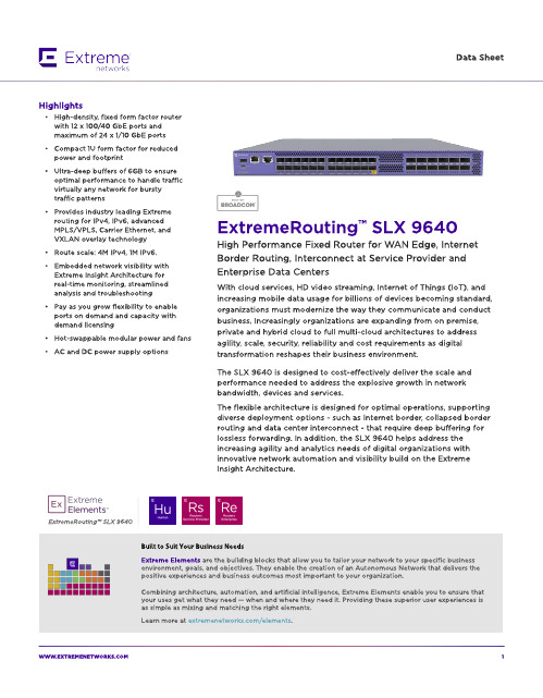
ExtremeRouting? SLX 9640
Built to Suit Your Business Needs Ext rem e Elem ent s are t he b uild ing b locks t hat allow you t o t ailor your net w ork t o your sp ecific b usiness environm ent , g oals, and ob ject ives. They enab le t he creat ion of an A ut onom ous Net w ork t hat d elivers t he p osit ive exp eriences and b usiness out com es m ost im p ort ant t o your org anizat ion.
W W W.EXTREMENETW
1
Flexib le Bo rd er Ro ut ing w it h Int ernet Scale, Ult ra-Deep Buffers,
MPLS and EVPN
The SLX 964 0 is a very p ow erful com p act d eep b uffer Int ernet b ord er rout er, p rovid ing a cost -efficient solut ion t hat is p urp ose-b uilt for t he m ost d em and ing service p rovid er and ent erp rise d at a cent ers and MA N/ WA N ap p licat ions. The rob ust syst em archit ect ure sup p ort ed by SLX-OS and a versat ile feat ure set includ ing IPv4 , IPv6, and MPLS/ VPLS w it h Carrier Et hernet 2.0 and OA M cap ab ilit ies t o p rovid e d ep loym ent flexib ilit y.
MB90F546GSPF中文资料

2
MB90540/540G/545/545G Series
(Continued) • UART 1 With full-duplex double buffer (8-bit length) Clock asynchronized or clock synchronized serial (extended I/O serial) can be used. • External interrupt circuit (8 channels) A module for starting an extended intelligent I/O service (EI2OS) and generating an external interrupt which is triggered by an external input. • Delayed interrupt generation module Generates an interrupt request for switching tasks. • 8/10-bit A/D converter (8 channels) 8/10-bit resolution can be selectively used. Starting by an external trigger input. Conversion time : 26.3 µs • FULL-CAN interfaces MB90540 series : 2 channel MB90545 series : 1 channel Conforming to Version 2.0 Part A and Part B Flexible message buffering (mailbox and FIFO buffering can be mixed) • External bus interface : Maximum address space 16 Mbytes • Package: QFP-100, LQFP-100
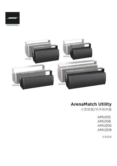
ArenaMatch Utility 小前景 补声扬声器 AMU105 AMU108 AMU206
规范信息
本产品符合所有适用的欧盟指令要求。您可以从网站 /compliance 找到完整的符合性声明。
此符号表示不得将此产品作为生活垃圾丢弃,应将其送到合适的 回收站点进行回收。正确处理和回收有助于保护自然资源、人类 健康和环境。想要获得更多关于此产品的处理和回收的信息,请 联系当地市政当局、垃圾处理服务部门或您购买此产品的商店。
中国危险物质限用表
有毒或有害物质或元素名称及成分
有毒或有害物质和元素
零件名称
铅
汞
(Pb) (Hg)
镉 ()
六价铬 (CR(VI))
多溴化 联苯 (PBB)
印刷电路板 X
O
O
O
O
金属零件
X
O
O
O
O
塑料零件
O
O
O
O
O
扬声器
X
O
O
O
O
线缆
X
O
O
O
O
此表格依据 SJ/T 11364 的要求制定。
O:表示此零件中所有均质材料所包含的此类有毒或有害物质均低于 GB/T 26572 中的限定要求。
6. 只能使用制造商指定的附件/配件。
7.
只能使用制造商指定或随本设备一起销售的推车、支架、
三角架、托架或工作台。如果使用推车,则在移动推车/设
备时应格外小心,以免因倾倒而造成伤害。
警告/小心:
包含可能导致窒息危险的小部件。不适合 3 岁以下的儿童使用。
本产品含有磁性材料。有关这是否会影响到您的植入式医疗器 械,请咨询您的医生。
包装清单................................................................................................................................................................................................... 5 可选配件................................................................................................................................................................................................... 5 检查和维护....................................................................................................................................................................................................... 6 保持防风雨性........................................................................................................................................................................................... 6 推荐使用的工具.............................................................................................................................................................................................. 6 产品尺寸........................................................................................................................................................................................................... 7 ArenaMatch Utility AMU105........................................................................................................................................................... 7 ArenaMatch Utility AMU108........................................................................................................................................................... 8 ArenaMatch Utility AMU206.......................................................................................................................................................... 9 ArenaMatch Utility AMU208........................................................................................................................................................ 10
MCC电路保护器说明书

FeaturesMaximum Ratings8.0 AmpSchottky Rectifier 20 to 100 VoltsElectrical Characteristics @ 25°C Unless Otherwise Specified•Operating Junction Temperature Range: -55⁰C to +150⁰C •Storage Temperature Range: -55⁰C to +150⁰C•High Current Capability •Low Forward Voltage•For Surface Mount Application•Lead Free Finish/RoHS Compliant(Note 1) ("P" Suffix D esignates Compliant. See O rdering I nformation)•Epoxy Meets UL 94 V-0 Flammability Rating •Moisture Sensitivity Level 1•Halogen Free. “Green” Device (Note 2)SK845L SK84545V 31.5V 45V SK835L SK83535V 24.5V 35V SK84L SK8440V 28V 40V SK82L SK8220V 14V 20V SK83L SK8330V 21V 30V MCC Part Number Device Marking MaximumRecurrent Peak Reverse VoltageMaximumRMS VoltageMaximum DCBlockingVoltageTypical Junction CapacitanceC J400pFMeasured at 1.0MHz,V R =4.0VMaximum DC Reverse Current a t Rated DC Blocking Voltage I R0.1m A 10m A T J =25⁰C ;T J =100⁰CPeak Forward Surge CurrentI FSM200A8.3ms,H alf S ineV F0.65V I F M =8.0A;Average Forward CurrentI F(AV)8.0A T L =95⁰C Maximum Instantaneous Forward Voltage0.80V Note:1.High Temperature Solder Exemptions Applied, S ee EU Directive Annex 7a .2.Halogen free "Green” products are defined as those which contain <900ppm bromine,<900ppm chlorine (<1500ppm total Br + Cl) and <1000ppm antimony compounds.3.Mounted on P.C.B. With 0.6" x 0.6" (16 mm x 16 mm) Copper Pad AreasSK82L-86L SK88L-810L T J =25⁰C SK86L SK88L SK810LSK86SK88SK81060V 60V 80V 80V 100V100V42V 56V 70V•Typical Thermal Resistance (Note 3) : 50o C/W Junction to Ambient •Typical Thermal Resistance (Note 3) : 18o C/W Junction to LeadCurve Characteristics25125150012345678910A v e r a g e F o r w a r d C u r r e n t (A)Fig. 1 - Forward Current Derating Curve5075100Lead Temperature (°C)1100255075100125150175200225P e a k F o r w a r d S u r g e C u r r e n t (A)Fig. 2 - Maximum Non-Repetitive Peak Forward Surge10Number of Cycles at 60 Hz0.020.050.20.525200.010.11100.00.10.20.30.40.50.60.70.80.91.0Instantaneous Forward Voltage (V)I n s t a n t a n e o u s F o r w a r d C u r r e n t (A )Fig. 3 - Typical Instantaneous Forward Characteristics0.020.050.20.525200.010.1110Instantaneous Forward Voltage (V)I n s t a n t a n e o u s F o r w a r d C u r r e n t (A )Fig. 4 - Typical Instantaneous Forward Characteristics110100100010000I n s t a n t a n e o u s R e v e r s e L e a k a g e C u r r e n t (μA )Fig. 5 - Typical Reverse Leakage CharacteristicsPercent of Rated Peak Reverse Voltage (%)0.1110100100010000I n s t a n t a n e o u s R e v e r s e L e a k a g e C u r r e n t (μA )Fig. 6 - Typical Reverse Leakage CharacteristicsPercent of Rated Peak Reverse Voltage (%)Ordering InformationDevice PackingPart Number-TP Tape&Reel: 3Kpcs/Reel。
商米特殊代码说明
特殊代码说明一、获取商米设备标识商米建议通过获取到以下内容来判断是否商米设备:1.设备的品牌名 brand(如:SUNMI)商米的品牌名统一为 SUNMI2.设备的系统型号 model(如:V1-B18)系统型号组成为产品型号+硬件特性+‘-’+软件特性其中以V、M、P、L开头为手持设备,以T、D、S开头为横屏设备(截至2017年12月)3.设备的ROM版本号(如:1.1.0)。
4.设备的ROM顺序号(如:128)。
可以下载Demo,仿照Demo在自己项目src下面新建android.os包(固定写法),将SystemProperties.java放入该包下,按以下方法获取指定的值:获取brand的代码为:String brand =SystemProperties.get("ro.product.brand");获取model的方法为:String model =SystemProperties.get("ro.product.model");获取ROM版本号的代码为:String versionname =SystemProperties.get("ro.version.sunmi_versionname");获取ROM顺序号的方法为:String versioncode =SystemProperties.get("ro.version.sunmi_versioncode");二、获取设备的SN号1.在AndroidManifest.xml中添加如下权限。
<uses-permission android:name="android.permission.READ_PHONE_STATE" />2.在需要的地方用以下代码获取商米SN号。
Class c =Class.forName("android.os.SystemProperties");Method get = c.getMethod("get",String.class);Log.i("sunmi", "the sn:" + (String)get.invoke(c, "ro.serialno")));Log.i("sunmi", "First four characters:" +(String) get.invoke(c, "ro.serialno").substring(0, 4)); } catch (Exception e) {e.printStackTrace();}3.在需要的地方用以下代码获取客户SN号,限定最多16位数字或大小写字母。
西门子PowerFlex 523变频器说明书

On Drive GuidePowerFlex 523 Adjustable Frequency AC Drive Parameter GroupsBasic Display b Output Freq b001 Commanded Freq b002 Output Current b003 Output Voltage b004 DC Bus Voltage b005Drive Status b006Fault 1 Code b007Fault 2 Code b008Fault 3 Code b009Process Display b010Control Source b012Contrl In Status b013Dig In Status b014Output RPM b015Output Speed b016Output Power b017Power Saved b018Elapsed Run Time b019Average Power b020Elapsed kWh b021Elapsed MWh b022Energy Saved b023Accum kWh Sav b024Accum Cost Sav b025Accum CO2 Sav b026Drive Temp b027Control Temp b028Control SW Ver b029Basic Program P Language P030 Motor NP Volts P031 Motor NP Hertz P032 Motor OL Current P033Motor NP FLA P034Motor NP Poles P035Motor NP RPM P036Voltage Class P038Torque Perf Mode P039Autotune P040Accel Time 1P041Decel Time 1P042Minimum Freq P043Maximum Freq P044Stop Mode P045Start Source 1P046Speed Reference1P047Start Source 2P048Speed Reference2P049Start Source 3P050Speed Reference3P051Average kWh Cost P052Reset To Defalts P053Terminal Blocks t DigIn TermBlk 02t062 DigIn TermBlk 03t063 2-Wire Mode t064 DigIn TermBlk 05t065DigIn TermBlk 06t066Relay Out1 Sel t076Relay Out1 Level t077Relay 1 On Time t079Relay 1 Off Time t080EM Brk Off Delay t086EM Brk On Delay t087Anlg In 0-10V Lo t091Anlg In 0-10V Hi t092Anlg In V Loss t094Anlg In4-20mA Lo t095Anlg In4-20mA Hi t096Anlg In mA Loss t097Anlg Loss Delay t098Analog In Filter t099Sleep-Wake Sel t100Sleep Level t101Sleep Time t102Wake Level t103Wake Time t104Communications C Comm Write Mode C121 RS485 Data Rate C123 RS485 Node Addr C124 Comm Loss Action C125Comm Loss Time C126RS485 Format C127Opt Data In 1C161Opt Data In 2C162Opt Data In 3C163Opt Data In 4C164Opt Data Out 1C165Opt Data Out 2C166Opt Data Out 3C167Opt Data Out 4C168MultiDrv Sel C169Drv 1 Addr C171Drv 2 Addr C172Drv 3 Addr C173Drv 4 Addr C174DSI I/O Cfg C175Advanced Display d Analog In 0-10V d360 Analog In 4-20mA d361 Elapsed Time-hr d362Elapsed Time-min d363Counter Status d364Timer Status d365Timer StatusF d366Drive Type d367Testpoint Data d368Motor OL Level d369Slip Hz Meter d375Speed Feedback d376DC Bus Ripple d380Output Powr Fctr d381Torque Current d382PID1 Fdbk Displ d383PID1 Setpnt Displ d384Fiber Status d390Advanced Program A Preset Freq 0A410 Preset Freq 1A411 Preset Freq 2A412 Preset Freq 3A413 Preset Freq 4A414 Preset Freq 5A415 Preset Freq 6A416 Preset Freq 7A417 Keypad Freq A426 MOP Freq A427 MOP Reset Sel A428 MOP Preload A429 MOP Time A430 Jog Frequency A431 Jog Accel/Decel A432 Purge Frequency A433 DC Brake Time A434DC Brake Level A435DC Brk Time@Strt A436DB Resistor Sel A437DB Threshold A438S Curve %A439PWM Frequency A440Accel Time 2A442Decel Time 2A443Accel Time 3A444Decel Time 3A445Accel Time 4A446Decel Time 4A447Skip Frequency 1A448Skip Freq Band 1A449Skip Frequency 2A450Skip Freq Band 2A451PID 1 Trim Hi A456PID 1 Trim Lo A457PID 1 Trim Sel A458PID 1 Ref Sel A459PID 1 Fdback Sel A460PID 1 Prop Gain A461PID 1 Integ Time A462PID 1 Diff Rate A463PID 1 Setpoint A464PID 1 Deadband A465PID 1 Preload A466PID 1 Invert Err A467Process Disp Lo A481Process Disp Hi A482Testpoint Sel A483Current Limit 1A484Shear Pin1 Level A486Shear Pin 1 Time A487Stall Fault Time A492Motor OL Select A493Motor OL Ret A494Drive OL Mode A495IR Voltage Drop A496Flux Current Ref A497Boost Select A530Start Boost A531Break Voltage A532Break Frequency A533Maximum Voltage A534Pulse In Scale A537Var PWM Disable A540Auto Rstrt Tries A541Auto Rstrt Delay A542Start At PowerUp A543Reverse Disable A544Flying Start En A545FlyStrt CurLimit A546Compensation A547Power Loss Mode A548Half Bus Enable A549Bus Reg Enable A550Fault Clear A551Program Lock A552Program Lock Mod A553Drv Ambient Sel A554Reset Meters A555Text Scroll A556Out Phas Loss En A557Max Traverse A567Traverse Inc A568Traverse Dec A569P Jump A570Sync Time A571Speed Ratio A572Network N This group contains parameters for the network option card that is installed.Additional parameters are listed on the next page.2 PowerFlex 523 Adjustable Frequency AC DriveAppView Parameter GroupsModifiedM This group contains parameters that have their values changed from the factory default.Fault and Diagnostic F Fault 4 Code F604Fault 5 Code F605Fault 6 Code F606Fault 7 Code F607Fault 8 Code F608Fault 9 Code F609Fault10 Code F610Fault 1 Time-hr F611Fault 2 Time-hr F612Fault 3 Time-hr F613Fault 4 Time-hr F614Fault 5 Time-hr F615Fault 1 Time-min F621Fault 2 Time-min F622Fault 3 Time-min F623Fault 4 Time-min F624Fault 5 Time-min F625Fault 1 Freq F631Fault 2 Freq F632Fault 3 Freq F633Fault 4 Freq F634Fault 5 Freq F635Fault 1 Current F641Fault 2 Current F642Fault 3 Current F643Fault 4 Current F644Fault 5 Current F645Fault 1 BusVolts F651Fault 2 BusVolts F652Fault 3 BusVolts F653Fault 4 BusVolts F654Fault 5 BusVolts F655Status @ Fault 1F661Status @ Fault 2F662Status @ Fault 3F663Status @ Fault 4F664Status @ Fault 5F665Comm Sts - DSI F681Comm Sts - Opt F682DSI I/O Act F686Drv 0 Logic Cmd F705Drv 0 Reference F706Drv 0 Logic Sts F707Drv 0 Feedback F708Drv 1 Logic Cmd F709Drv 1 Reference F710Drv 1 Logic Sts F711Drv 1 Feedback F712Drv 2 Logic Cmd F713Drv 2 Reference F714Drv 2 Logic StsF715Drv 2 Feedback F716Drv 3 Logic Cmd F717Drv 3 Reference F718Drv 3 Logic Sts F719Drv 3 Feedback F720Drv 4 Logic Cmd F721Drv 4 Reference F722Drv 4 Logic Sts F723Drv 4 Feedback F724DSI Errors F731Conveyor G1Language P030Output Freq b001Commanded Freq b002Motor NP Volts P031Motor NP Hertz P032Motor OL Current P033Motor NP FLA P034Motor NP Poles P035Autotune P040Accel Time 1P041Decel Time 1P042Minimum Freq P043Maximum Freq P044Stop Mode P045Start Source 1P046Speed Reference1P047DigIn TermBlk 02t062DigIn TermBlk 03t063Relay Out1 Sel t076Anlg In 0-10V Lo t091Anlg In 0-10V Hi t092Anlg In4-20mA Lo t095Anlg In4-20mA Hi t096Anlg In mA Loss t097Slip Hz Meter d375Preset Freq 0A410Jog Frequency A431Jog Accel/Decel A432S Curve %A439Reverse DisableA544Mixer G2Language P030Output Freq b001Commanded Freq b002Output Current b003Motor NP Volts P031Motor NP Hertz P032Motor OL Current P033Motor NP FLA P034Motor NP Poles P035Autotune P040Accel Time 1P041Decel Time 1P042Minimum Freq P043Maximum Freq P044Stop Mode P045Start Source 1P046Speed Reference1P047Relay Out1 Sel t076Anlg In 0-10V Lo t091Anlg In 0-10V Hi t092Anlg In4-20mA Lo t095Anlg In4-20mA Hi t096Anlg In mA Losst097Preset Freq 0A410Stall Fault Time A492Compressor G3Language P030Output Freq b001Commanded Freq b002Motor NP Volts P031Motor NP Hertz P032Motor OL Current P033Motor NP FLA P034Motor NP Poles P035Autotune P040Accel Time 1P041Decel Time 1P042Minimum FreqP043Maximum FreqP044Stop Mode P045Start Source 1P046Speed Reference1P047Relay Out1 Sel t076Anlg In 0-10V Lo t091Anlg In 0-10V Hi t092Anlg In4-20mA Lo t095Anlg In4-20mA Hi t096Anlg In mA Loss t097Preset Freq 0A410Auto Rstrt Tries A541Auto Rstrt Delay A542Start At PowerUp A543Reverse Disable A544Power Loss Mode A548Half Bus Enable A549Centrifugal Pump G4Language P030Output Freq b001Commanded Freq b002Motor NP Volts P031Motor NP Hertz P032Motor OL Current P033Motor NP FLA P034Motor NP Poles P035Autotune P040Accel Time 1P041Decel Time 1P042Minimum Freq P043Maximum Freq P044Stop Mode P045Start Source 1P046Speed Reference1P047Relay Out1 Sel t076Anlg In 0-10V Lo t091Anlg In 0-10V Hi t092Anlg In4-20mA Lo t095Anlg In4-20mA Hi t096Anlg In mA Loss t097Preset Freq 0A410PID 1 Trim Hi A456PID 1 Trim Lo A457PID 1 Ref Sel A459PID 1 Fdback Sel A460PID 1 Prop Gain A461PID 1 Integ Time A462PID 1 Diff Rate A463PID 1 Setpoint A464PID 1 Deadband A465PID 1 Preload A466Auto Rstrt Tries A541Auto Rstrt Delay A542Start At PowerUp A543Reverse Disable A544Blower/Fan G5Language P030Output Freq b001Commanded Freq b002Motor NP Volts P031Motor NP Hertz P032Motor OL Current P033Motor NP FLAP034Motor NP Poles P035Autotune P040Accel Time 1P041Decel Time 1P042Minimum Freq P043Maximum Freq P044Stop Mode P045Start Source 1P046Speed Reference1P047Relay Out1 Sel t076Anlg In 0-10V Lo t091Anlg In 0-10V Hi t092Anlg In4-20mA Lo t095Anlg In4-20mA Hi t096Anlg In mA Loss t097Preset Freq 0A410PID 1 Trim Hi A456PID 1 Trim Lo A457PID 1 Ref Sel A459PID 1 Fdback Sel A460PID 1 Prop Gain A461PID 1 Integ Time A462PID 1 Diff Rate A463PID 1 Setpoint A464PID 1 Deadband A465PID 1 Preload A466Auto Rstrt Tries A541Auto Rstrt Delay A542Start At PowerUp A543Reverse Disable A544Flying Start En A545Additional groups are listed on the next page.PowerFlex 523 Adjustable Frequency AC Drive 3CustomView Parameter GroupFault DescriptionsExtruder G6Language P030Output Freq b001Commanded Freq b002Output Current b003Motor NP Volts P031Motor NP Hertz P032Motor OL Current P033Motor NP FLA P034Motor NP Poles P035Autotune P040Accel Time 1P041Decel Time 1P042Minimum Freq P043Maximum Freq P044Stop Mode P045Start Source 1P046Speed Reference1P047Relay Out1 Sel t076Anlg In 0-10V Lo t091Anlg In 0-10V Hi t092Anlg In4-20mA Lo t095Anlg In4-20mA Hi t096Anlg In mA Loss t097Slip Hz Meter d375Speed Feedback d376Preset Freq 0A410Stall Fault Time A492Pulse In Scale A537Power Loss Mode A548Half Bus Enable A549Textile/Fiber G8Language P030Output Freq b001Commanded Freq b002Motor NP Volts P031Motor NP Hertz P032Motor OL Current P033Motor NP FLA P034Motor NP Poles P035Autotune P040Accel Time 1P041Decel Time 1P042Minimum Freq P043Maximum Freq P044Stop Mode P045Start Source 1P046Speed Reference1P047DigIn TermBlk 02t062DigIn TermBlk 03t063Relay Out1 Sel t076Anlg In 0-10V Lo t091Anlg In 0-10V Hi t092Anlg In4-20mA Lo t095Anlg In4-20mA Hi t096Anlg In mA Loss t097Slip Hz Meter d375Fiber Status d390Preset Freq 0A410Jog Frequency A431Jog Accel/Decel A432S Curve %A439Reverse Disable A544Power Loss Mode A548Half Bus Enable A549Bus Reg Enable A550Max Traverse A567Traverse Inc A568Traverse Dec A569P Jump A570Sync Time A571Speed Ratio A572CustomGCThis group can store up to 100 of your frequently used parameters for your application.No.Fault Type (1)Description ActionF000No Fault –No fault present.–F002Auxiliary Input 1External trip (Auxiliary) input.•Check remote wiring.•Verify communications programming for intentional fault.F003Power Loss 2Single phase operation detected with excessive load.•Monitor the incoming AC line for low voltage or line power interruption.•Check input fuses.•Reduce load.F004UnderVoltage 1DC bus voltage fell below the minimum value.Monitor the incoming AC line for low voltage or line powerinterruption.F005OverVoltage1DC bus voltage exceeded maximum value.Monitor the AC line for high line voltage or transient conditions. Busovervoltage can also be caused by motor regeneration. Extend thedecel time or install dynamic brake option.F006Motor Stalled 1Drive is unable to accelerate or decelerate motor.•Increase P041, A442, A444, A446 [Accel Time x] or reduce load so drive output current does not exceed the current set byparameter A484 [Current Limit 1] for too long.•Check for overhauling load.F007Motor Overload 1Internal electronic overload trip.•An excessive motor load exists. Reduce load so drive output current does not exceed the current set by parameterP033 [Motor OL Current].•Verify A530 [Boost Select] setting.F008Heatsink OvrTmp 1Heatsink/Power Module temperature exceeds a predefined value.•Check for blocked or dirty heat sink fins. Verify that ambienttemperature has not exceeded the rated ambient temperature.•Check fan.F009CC OvrTmp 1Control module temperature exceeds a predefined value.•Check product ambient temperature.•Check for airflow obstruction.•Check for dirt or debris.•Check fan.F012HW OverCurrent 2The drive output current has exceeded the hardware current limit.Check programming. Check for excess load, improper A530 [BoostSelect] setting, DC brake volts set too high or other causes of excesscurrent.Additional faults are listed on the next page.4 PowerFlex 523 Adjustable Frequency AC DriveF013Ground Fault2 A current path to earth ground has been detected at one or more ofthe drive output terminals.Check the motor and external wiring to the drive output terminals for a grounded condition.F021Output Ph Loss1Output Phase Loss (if enabled).Configure with A557 [Output Phas Loss En].•Verify motor wiring.•Verify motor.F029Analog In Loss1An analog input is configured to fault on signal loss. A signal loss hasoccurred.Configure with t094 [Anlg In V Loss] or t097 [Anlg In mA Loss].•Check for broken/loose connections at inputs.•Check parameters.F033Auto Rstrt Tries2Drive unsuccessfully attempted to reset a fault and resume runningfor the programmed number of A541 [Auto Rstrt Tries].Correct the cause of the fault and manually clear.F038Phase U to Gnd2 A phase to ground fault has been detected between the drive andmotor in this phase.•Check the wiring between the drive and motor.•Check motor for grounded phase.•Replace drive if fault cannot be cleared.F039Phase V to Gnd F040Phase W to GndF041Phase UV Short2Excessive current has been detected between these two outputterminals.Check the motor and drive output terminal wiring for a shorted condition.Replace drive if fault cannot be cleared.F042Phase UW ShortF043Phase VW ShortF048Params Defaulted1The drive was commanded to write default values to EEPROM.•Clear the fault or cycle power to the drive.•Program the drive parameters as needed.F063SW OverCurrent1Programmed A486 [Shear Pin1 Level] has been exceeded for a timeperiod greater than the time programmed in A487 [Shear Pin 1Time].•Verify connections between motor and load.•Verify level and time requirements.F064Drive Overload2Drive overload rating has been exceeded.Reduce load or extend Accel Time.F070Power Unit2Failure has been detected in the drive power section.•Check maximum ambient temperature has not been exceeded.•Cycle power.•Replace drive if fault cannot be cleared.F071DSI Net Loss2Control over the Modbus or DSI communications link has beeninterrupted.•Cycle power.•Check communications cabling.•Check Modbus or DSI setting.•Check Modbus or DSI status.F072Opt Net Loss2Control over the network option card’s remote network has beeninterrupted.•Cycle power.•Check communications cabling.•Check network adapter setting.•Check external network status.F080Autotune Failure2The autotune function was either cancelled by the user or failed.Restart procedure.F081DSI Comm Loss2Communications between the drive and the Modbus or DSI masterdevice have been interrupted.•Cycle power.•Check communications cabling.•Check Modbus or DSI setting.•Check Modbus or DSI status.•Modify using C125 [Comm Loss Action].•Connecting I/O terminals C1 and C2 to ground may improve noise immunity.•Replace wiring, Modbus master device, or control module.F082Opt Comm Loss2Communications between the drive and the network option cardhave been interrupted.•Cycle power.•Reinstall option card in drive.•Modify using C125 [Comm Loss Action].•Replace wiring, port expander, option card, or control module.F094Function Loss2“Freeze-Fire” (Function Loss) input is inactive, input to theprogrammed terminal is open.Close input to the terminal and cycle power.F100ParameterChksum2Drive parameter non-volatile storage is corrupted.Set P053 [Reset To Defalts] to 2 “Factory Rset”.F101External Storage2External non-volatile storage has failed.Set P053 [Reset To Defalts] to 2 “Factory Rset”.F105 C Connect Err2Control module was disconnected while drive was powered.Clear fault and verify all parameter settings. Do not remove orinstall the control module while power is applied.F106Incompat C-P2The control module could not recognize the power module.•Cycle power.•Flash with newer firmware version.•Replace drive if fault cannot be cleared.F107Replaced C-P2The control module was mounted to a power module with a differentpower rating.Set P053 [Reset To Defalts] to any of the reset options.Additional faults are listed on the next page.Publication 520-DU002A-EN-E - September 2013 -Copyright © 2013 Rockwell Automation, Inc. All rights reserved.Allen-Bradley, Rockwell Automation, PowerFlex, and TechConnect are trademarks of Rockwell Automation, Inc.Trademarks not belonging to Rockwell Automation are property of their respective companies.Power, Control and Information Solutions HeadquartersAmericas: Rockwell Automation, 1201 South Second Street, Milwaukee, WI 53204-2496 USA, T el: (1) 414.382.2000, Fax: (1) 414.382.4444Europe/Middle East/Africa: Rockwell Automation NV, Pegasus Park, De Kleetlaan 12a, 1831 Diegem, Belgium, T el: (32) 2 663 0600, Fax: (32) 2663 0640Asia Pacific: Rockwell Automation, Level 14, Core F, Cyberport 3, 100 Cyberport Road, Hong Kong, T el: (852) 2887 4788, Fax: (852) 2508 1846All the recommended documentation listed in this section is available online at /literature .The following publications provide general drive information:The following publications provide specific PowerFlex 520-Series information on drive installation, features, specifications, and service:The following publications provide specific Network Communications information:F109Mismatch C-P 2The control module was mounted to a different drive type power module.Set P053 [Reset To Defalts] to any of the reset options.F110KeypadMembrane 2Keypad membrane failure / disconnected.•Cycle power.•Replace control module if fault cannot be cleared.F114uC Failure 2Microprocessor failure.•Cycle power.•Replace control module if fault cannot be cleared.F122I/O Board Fail 2Failure has been detected in the drive control and I/O section.•Cycle power.•Replace drive or control module if fault cannot be cleared.F125Flash Update Req 2The firmware in the drive is corrupt, mismatched, or incompatible with the hardware.Perform a firmware flash update operation to attempt to load a valid set of firmware.F126NonRecoverablErr2A non-recoverable firmware or hardware error was detected. The drive was automatically stopped and reset.•Clear fault or cycle power to the drive.•Replace drive or control module if fault cannot be cleared.F127DSIFlashUpdatReq 2A critical problem with the firmware was detected and the drive is running using backup firmware that only supports DSI communications.Perform a firmware flash update operation using DSI communications to attempt to load a valid set of firmware.(1)Type 1 = Auto-Reset/Run faults. Type 2 = Non-Resettable faults.TitlePublication Wiring and Grounding Guidelines for Pulse Width Modulated (PWM) AC Drives DRIVES-IN001 Preventive Maintenance of Industrial Control and Drive System EquipmentDRIVES-TD001 Safety Guidelines for the Application, Installation and Maintenance of Solid State Control SGI-1.1 A Global Reference Guide for Reading Schematic Diagrams 100-2.10 Guarding Against Electrostatic Damage8000-4.5.2TitlePublication PowerFlex 520-Series Adjustable Frequency AC Drive User Manual 520-UM001 PowerFlex 520-Series AC Drive Specifications 520-TD001 PowerFlex Dynamic Braking Resistor Calculator PFLEX-AT001 PowerFlex AC Drives in Common Bus ConfigurationsDRIVES-AT002TitlePublication PowerFlex 25-COMM-D DeviceNet Adapter User Manual520COM-UM002 PowerFlex 25-COMM-E2P Dual-Port EtherNet/IP Adapter User Manual 520COM-UM003 PowerFlex 25-COMM-P PROFIBUS DP Adapter520COM-UM004。
酷玛QM3G YHSC 触摸屏PLC一体机使用手册说明书

感谢您购买 C oolmay QM3G 系列一体机。
本手册主要说明该系列触摸屏PLC一体机的产品特性、一般规格和接线方法。
详细PLC编程请参见《Coolmay QM3G 系列一体机编程手册》;触摸屏部分参见《Coolmay TP 系列人机界面使用手册》。
产品信息1公司产品系列 : 系列2HMI类型 43: 4.3寸 50: 5寸 70/70H D /70K : 7寸 100: 10寸3输入输出点数 16: 8入8出 24: 12入12出 38: 20入18出 44: 24入20出 60: 30入30出等4模块分类 M: 通用控制器主模块5开关量输出类型 R: 继电器输出类型; T: 晶体管(MOS 管)输出类型; RT: 混合输出6模拟量输入点数 43/50可选4路,70/HD 可选12路,70K /100可选16路 7模拟量输出点数 43/50可选2路,70/70HD /70K /100可选8路8模拟量输入类型 E : E 型热电偶K PT :PT100 PT1000:PT1000 NTC :热敏电阻(10K /50K /100K ) A0: 0-20mA电流 A4: 4-20mA电流 V5: 0-5V电压 V: 0-10V电压 V5_:-5V ~5V 电压 V _:-10~10V 电压【仅7寸和10寸的可选负电压输入】 9模拟量输出类型 A0: 0-20mA 电流 A4: 4-20mA 电流 V5: 0-5V 电压 V : 0-10V 电压 V5_:-5V ~5V 电压 V _:-10~10V 电压【仅7寸和10寸的可选负电压输出,且占用两路DA 】10. C1表示单相高速计数,C2表示AB 相计数,C3表示ABZ 相计数;11P 表示高速脉冲;P表示高速脉冲;12选装通讯口 参见【表一:基本参数】. . . . . . . . . . 常规8路,高速计数+高速脉冲总发不能超过480KHz .QM3G QM3G FH FH FH FH FH FH FH FH FH FH FH FH FH FH FH (可定制型/T 型/S 型/J 型,支持负温) 常规单相6路60KHz 或AB (Z )相2路30KHz +AB 相 1 路5KHz010KHz 100KHz Y0-Y3为100KHz ,Y4-Y7为10KHz ; 命名规则QM3G 43FH 图1 安装尺寸图QM3G -100FHQM3G -43FHQM3G -70KFH电气设计参考产品构造RUN :PLC运行指示灯COM PLC与触摸屏 : 通讯上时快闪QM3G -43FH图3图6 -70KFHQM3G 硬件接口安装尺寸机械设计参考输入为ON 输入为OFF 滤波功能高数计数功能有滤波功能,滤波时间在0-60ms范围内可设,默认是10ms开关量继电器输出指标允许最大电流回路电源电压电路绝缘On响应时间机械寿命(无负载)电气寿命(额定负载)2A /点,4A /4点 COM ,5A /8点 COM ,5A /12点 COMDC 30V以下/AC 220V以下继电器机械绝缘约10ms1000万次30万次开关量晶体管(MOS 管)输出指标允许最大电流回路电源电压电路绝缘隔离电压(电源-外部端子)On响应时间高速输出频率MOS 管: 2A /点, 4A /4点 C OM ,5A /12点C OM :MT :0.5A /点,0.8A /4点 C OM , 1.6A /12点 C OMDC24V 光耦绝缘1500VAC高速输出:10μs;其他:0.5ms 模拟量输入指标输入信号响应时间模拟量输入点数精度PT100/PT1000/热电偶/NTC/0-10V/0-5V /-10~10V /-5~5V /0-20mA/4-20mA/1个扫描周期0-16路12位模拟量输出指标输出信号模拟量输出点数精度0-5V/0-10V/0-20mA/4其他按客户要求定制信号等-10~10V /-5~5V /-20mA/0-8路12位外部接口通讯口环境条件工作温度相对湿度储存温度振动频率0°C~50°C5%~95%RH -20°C~70°C10-57Hz,振幅0.035mm; 57Hz-150Hz,加速度4.9m/s ² (X、Y、Z三方向各10次,合计各80分钟)基本参数触摸屏PLC一体机常见型号规格QM3G -43FH /50-16MR FH QM3G FH FH -70K /100-38M R QM3G FH FH --48M R 70K /100开关量模拟量(最大可选)通讯口(可选)高速计数高速脉冲DI DO AD DA 触摸屏PLC 单相AB相ABZ相输出2018242443FH /50FH:MT 为MOS 管输出;70FH /70HD 70KFH /100FH :MT 时Y0-Y3 为MOS 管输出,Y4-Y35 为晶体管输出;MR 为继电器输出;MRT 为混合输出。
MTK手机暗码大全
MMS1.0
MMS1.1
⑤Offine page (脱机网页)开启后手机上网可存下网页
11,J2METCK确定-进入JAVA工程模式
Normal(标准)
CLDCTCK(意义均未知)
MIDPTCK
WMAPITCK
MMAPITCK
12,AMR
13,TOUCH SCREEN
14,VIDEO HIGH BITRATE
*#357#软件版本
*#753#硬件测试
*##选出厂设置,
工程模式*##;*#36565#
一,网络号码,不用介绍,看不懂,最好还是不要乱动,动了也应该没什么用二,设备
1,LCD-主屏幕:
①set contrast(设置对比度)确定后显示
set param(设置参数)数字可调整
②set biasratio(设置偏差比率)
方向键下LF:
方向键左RT:
方向键右
┃LSK:
左软键(一点都没觉得软)RSK:
有软键(还不如左软键)
┃Snd:
接通键End:
挂机键Vup:
音量大Vdn:
音量小
┃1 2 3 4 5 6 7 8 9 0 * #:
数字键及*#
┃测试完成后会出现Pass ┃┣━━Vibrator震动测试选“开”测试震动功能是否可用┃┣━━Loud Spk扬声器(我一直想说“喇叭”)测试选“开”测试扬声器是否可以发声┃┣━━铃声(原本就是中文)铃声测试选“开”测试铃声功能是否正常┃┣━━LED发光二极管指示灯(彩灯)测试
③set line rate(设置线路速率)
④set temperature(设置温度)
⑤set COLOR(设置颜色)
Freescale Kinetis E 系列 KE06 微控制器开发板用户指南说明书

Freescale Semiconductor User’s Guide1FRDM-KE06 hardware overviewThe FRDM-KE06 Freedom development platform microcontroller board is assembled with the following features:•Kinetis E series KE06 MCU in an 80-pin LQFP package•On-board serial and debug adapter (OpenSDA)•I/O headers for easy access to MCU I/O pins •Freescale inertial sensor, MMA8451Q •Reset push button •RGB LED•Infrared communication •One thermistor•Motor control function for simple BLDC motor control on APMOTOR56F8000E •CAN communication Figure 1 shows a block diagram of the FRDM-KE06 board.Document Number:FRDMKE06UGRev. 0, 03/2014Contents1.FRDM-KE06 hardware overview . . . . . . . . . . . . . . . . 12.FRDM-KE06 hardware description . . . . . . . . . . . . . . 23.Serial and Debug Adapter (OpenSDA) . . . . . . . . . . . 4Freedom KE06 User’s Guideby: Freescale Semiconductor, Inc.FRDM-KE06 hardware descriptionFigure1. FRDM-KE06 block diagramThe FRDM-KE06 features two microcontrollers, the target MCU and a serial and debug adapter (OpenSDA) MCU. The target MCU is a Kinetis E series KE06 family device. The OpenSDA MCU is a Kinetis K series K20 family device, the K20DX128VFM5.2FRDM-KE06 hardware description2.1Power supplyThe FRDM-KE06 offers a design with multiple power supply options. It can be powered from the USB connector, the V IN pin on the I/O header, an off-board 1.71-3.6V supply from the 3.3V pin on the I/O header or 3.3V from motor control board. The USB and V IN supplies are regulated on-board using a 3.3V linear regulator to produce the main power supply. The other two sources are not regulated on-board. Note that KE06 on FRDM board can be powered by 5V or 3.3V.The following figure shows the schematic drawing for the power supply inputs and the on-board voltage regulator.FRDM-KE06 hardware descriptionFigure 2. FRDM-KE06 power supplyTable 1 provides the operational details and requirements for the power supplies.Note that the OpenSDA circuit is only operational when a USB cable is connected and supplying power to J6. However, the protection circuitry is in place to allow multiple sources to be powered at once.Table 1. Power supply requirementsSupply Source Valid RangeOpenSDA Operational?Regulated on-board?OpenSDA USB (J6)5VYes Yes V IN Pin on I/O header 4.3-9V Yes Yes 3.3V Pin on I/O header 1.71-3.6V Yes No 3.3V Pin on motor control header3.3VYesNoTable 2. Power suppliesPower Supply Name DescriptionVDD_PERIPHPeripheral power supply, including RGB LED, Key buttons, infrared, thermistor, reset circuit.J14 Pin1&2 connected, 3.3V power supply;J14 Pin2&3 connected, 5V power supply.Serial and Debug Adapter (OpenSDA)Notes:1.J9 and J10 are not populated by default on the production version. The two pins of these headers are shorted together by 0 ohm resistor R12 and R26 on the PCB. To measure the energyconsumption of either the KE06 or the OpenSDA MCU, the 0 ohm resistor between these pins must first be cut. A current probe or a shunt resistor and voltage meter can then be applied to measure the energy consumption on these rails. When the MCU current measurement is done, this 0 ohm resistor can be soldered on again.2.To better get ADC accuracy on KE06, it is recommended that a 0 ohm resistor R13 be soldered on. Ensure there is no power supply from P3V3_MOTOR and P3V3 sourced from I/O headers.3Serial and Debug Adapter (OpenSDA)OpenSDA is an open-standard serial and debug adapter. It bridges serial and debug communications between a USB host and an embedded target processor as shown in Figure 3.VDD_KE06KE06 MCU power supply.Header J9 provides a convenient means for KE06 energy consumption measurements.Header J14 for KE06 power supply selection: 3.3V or 5V.J14 Pin1&2 connected, 3.3V power supply,J14 Pin2&3 connected, 5V power supply.P3V3_SDAOpenSDA circuit power supply. Can be 3.3V only.Header J10 provides a convenient means for K20 energy consumption measurements.P5V_SDA INPUT [J6 Pin1] Input 5V Power supplied from the OpenSDA USB connector. P5-9V_VIN INPUT [J4 Pin16] Power supplied from the V IN pin of the I/O headers.P3V3_MOTOR INPUT [J2 Pin13] Input 3.3V power supplied from motor control header.P5V_USB OUTPUT[J4 Pin10] Output 5V to the I/O headers.Sourced from J6 USB (P5V_SDA) supply through a back drive protection Schottky diode.Table 2. Power suppliesSerial and Debug Adapter (OpenSDA)Figure3. OpenSDA block diagramOpenSDA is managed by a Kinetis K20 MCU built on the ARM® Cortex™-M4 core. The OpenSDA circuit includes a status LED (D4) and a reset pushbutton (SW1). The pushbutton asserts the reset signal to the KE06 target MCU. It can also be used to place the OpenSDA circuit into Bootloader mode by holding down the reset pushbutton while plugging the USB cable to USB connector J6. Once the OpenSDA enters bootloader mode, other OpenSDA applications such as debug app can be programmed. SPI and GPIO signals provide an interface to the SWD debug port of the KE06. Additionally, signal connections are available to implement a UART serial channel. The OpenSDA circuit receives power when the USB connector J6 is plugged into a USB host.3.1Debugging InterfaceSignals with SPI and GPIO capability are used to connect directly to the SWD of the KE06. These signals are also brought out to a standard 10-pin (0.05”) Cortex Debug connector (J7) as shown in Figure 4. It is possible to isolate the KE06 MCU from the OpenSDA circuit and use J7 to connect to an off-board MCU. To accomplish this, cut the 0 ohm resistor R58. This will disconnect the SWD_CLK pin to the KE06 so that it will not interfere with the communications to an off-board MCU connected to J7.When KE06 on FRDM board is 5V powered, and the OpenSDA is power off, there need to connect an external debugger to debug KE06 on board.Serial and Debug Adapter (OpenSDA)Figure4. SWD debug connector to KE063.2Virtual Serial PortA serial port connection is available between the OpenSDA MCU and UART1 pin PTC7 (TXD1) and PTC6 (RXD1) of KE06. Several of the default OpenSDA applications provided by Freescale, including the MSD Flash Programmer and the P&E Debug Application, provide a USB Communications Device Class (CDC) interface that bridges serial communications between the USB host and this serial interface on the KE06.3.3KE06 Microcontroller3.3.1Clock SourceThe Kinetis KE06 microcontrollers feature an on-chip oscillator compatible with two ranges of input crystal or resonator frequencies: 32 kHz (low frequency mode), 4-20 MHz (high frequency mode).The KE06 on the FRDM-KE06 is clocked from an 8 MHz crystal.3.3.2Serial PortThe serial port interface signals used with OpenSDA are UART1 pin PTC7 (TXD1) and PTC6 (RXD1). These signals are also connected to I/O header J1.3.3.3ResetThe PTA5/RESET signal on the KE06 is connected externally to a pushbutton SW1. The reset button can be used to force an external reset event in the target MCU. The reset button can also be used to force the OpenSDA circuit into bootloader mode when plugging the USB cable to J6. See Section3, “Serial and Debug Adapter (OpenSDA)” section for more details.Serial and Debug Adapter (OpenSDA)3.3.4DebugThe sole debug interface on all Kinetis E Series devices is a Serial Wire Debug (SWD) port. The primary controller of this interface on the FRDM-KE06 is the onboard OpenSDA circuit. However, a 2x5-pin (0.05”) Cortex Debug connector, J7, provides access to the SWD signals for the KE06 MCU. The following table shows SWD connector signals description for KE06:3.4ThermistorOne thermistor (RT1) is connected to two ADC inputs (PTF4/ADP12, PTF5/ADP13) of KE06 for evaluating the ADC module.Figure 5. Thermistor connectionTable 3. ARM JTAG/SWD mini Connector DescriptionPin FunctionConnection to KE061VTref 3.3V or 5V KE06 power supply (VDD_KE06)2SWDIO/TMS PTA4/SWD_DIO 3GNDGND4SWDCLK/TCK PTC4/SWD_CLK 5GND GND 6SWO/TDO NC 7NC NC 8TDI NC 9NC NC10RESETPTA5/RESETSerial and Debug Adapter (OpenSDA)3.5Infrared PortOne infrared Rx port and one Tx port (as shown in the following figure) are connected to ACMP0 input pin (ACMP0_IN1) and UART0 TXD0 pin of KE06 to demonstrate the capability of SCI0 modulated by a flextimer to generate infrared signals and use ACMP0 as a filter to receive the SCI data via infrared signal.Figure6. Infrared connection3.6Key buttonsTwo key buttons are connected to PTH3/4 to demonstrate KBI function of KE06, which can capture both falling edge and rising edge of key button input, as shown in the following figure.Serial and Debug Adapter (OpenSDA)Figure7. Key buttons connection3.7Three-axis accelerometerA Freescale MMA8451Q low power, three-axis accelerometer is interfaced through an I2C bus and two GPIO signals as shown in the following table. By default, the I2C address is 0x1D (SA0 pulled high).Table4. Accelerometer signal connectionsMMA8451Q KE06SCL PTA3SDA PTA2INT1 PTD4INT2 PTD3Serial and Debug Adapter (OpenSDA)Figure8. Accelerometer connection3.8RGB LEDThree PWM-capable pins are connected to a red, green, blue LED. The signal connections are shown in the table below.Table5. RGB LED Signal ConnectionsRGB LED KE06Red Cathode PTG5/FTM2CH3Green Cathode PTG6/FTM2CH4Blue Cathode PTG7/FTM2CH5Serial and Debug Adapter (OpenSDA)Figure9. GB LED connection3.9CANThe CAN phy on KE06 FRDM board is 3.3V powered.Table6. CAN signal connectionCAN Phy KE06D CAN_TXR CAN_RXSerial and Debug Adapter (OpenSDA)Figure10. CAN3.10Input/Output HeadersThe KE06 microcontroller is packaged in an 80-pin LQFP. Some pins are utilized in on-board circuitry, but many are directly connected to one of four I/O headers (J1, J2, J3, J4 and J5). J1 and J2 also function as motor control headers to provide access to a motor control board such as simple BLDC motor driving board APMOTOR56F8000E.Serial and Debug Adapter (OpenSDA)Figure11. I/O headers3.11Arduino CompatibilityThe I/O headers on the FRDM-KE06 are arranged to allow compatibility with peripheral boards (known as shields) that connect to Arduino and Arduino-compatible microcontroller boards. The pins on the headers share the same mechanical spacing and placement as the I/O headers on the Arduino Uno Revision 3 board design. See Figure11 for compatible signals.Document Number:FRDMKE06UG Rev. 003/2014Information in this document is provided solely to enable system and software implementers to use Freescale products. There are no express or implied copyright licenses granted hereunder to design or fabricate any integrated circuits based on the information in this document.Freescale reserves the right to make changes without further notice to any products herein. Freescale makes no warranty, representation, or guarantee regarding the suitability of its products for any particular purpose, nor does Freescale assume any liability arising out of the application or use of any product or circuit, and specifically disclaims any and all liability, including without limitation consequential or incidental damages. “Typical” parameters that may be provided in Freescale data sheets and/or specifications can and do vary in different applications, and actual performance may vary over time. All operating parameters, including “typicals,” must be validated for each customer application by customer’s technical experts. Freescale does not convey any license under its patent rights nor the rights of others. Freescale sells products pursuant to standard terms and conditions of sale, which can be found at the following address: /SalesTermsandConditions.How to Reach Us:Home Page:Web Support:/supportFreescale, the Freescale logo, and Kinetis, are trademarks of FreescaleSemiconductor, Inc., Reg. U.S. Pat. & Tm. Off. All other product or service names arethe property of their respective owners. ARM and Cortex are the registered trademarksof ARM Limited. ARMCortex-M4 is the trademark of ARM Limited.© 2014 Freescale Semiconductor, Inc.。
MGate MB3660 Series MCC Tool for Linux 发布说明书

Utility for MGate MB3660 Series (MCC Tool for Linux) ReleaseNotesSupported Operating SystemsNotesChangesApplicable ProductsBugs FixedN/AN/AEnhancementsLinux Kernel 2.6.x, Linux Kernel 3.x, Linux Kernel 4.xMGate MB3180, MGate MB3280, MGate MB3480, MGate MB3170, MGate MB3170I, MGate MB3270,MGate MB3270I, MGate MB3170-T, MGate MB3170I-T, MGate MB3270-T, MGate MB3270I-T, MGate MB3170-M-SC, MGate MB3170-M-ST, MGate MB3170-S-SC, MGate MB3170I-M-SC, MGate MB3170I-S-SC, MGate MB3170-M-SC-T, MGate MB3170-M-ST-T, MGate MB3170-S-SC-T, MGate MB3170I-M-SC-T, MGate MB3170I-S-SC-T, MGate MB3660-8-J-2AC, MGate MB3660I-16-2AC,MGate MB3660-16-J-2AC, MGate MB3660-8-2AC, MGate MB3660-8-2DC, MGate MB3660I-8-2AC,MGate MB3660-16-2AC, MGate MB3660-16-2DC, NPort 5110A, NPort 5110A-T, NPort 5130A, NPort 5130A-T, NPort 5150A, NPort 5150A-T, NPort 5210A, NPort 5210A-T, NPort 5230A, NPort 5230A-T,NPort 5250A, NPort 5250A-T, NPort 5150AI-M12, NPort 5150AI-M12-CT, NPort 5150AI-M12-T, NPort 5150AI-M12-CT-T, NPort 5250AI-M12, NPort 5250AI-M12-CT, NPort 5250AI-M12-T, NPort 5250AI-M12-CT-T, NPort 5450AI-M12, NPort 5450AI-M12-CT, NPort 5450AI-M12-T, NPort 5450AI-M12-CT-T,NPort 6150, NPort 6150-T, NPort 6250, NPort 6250-M-SC, NPort 6250-S-SC, NPort 6250-T, NPort 6250-M-SC-T, NPort 6250-S-SC-T, NPort 6450, NPort 6450-T, NPort 6610-8, NPort 6610-8-48V,NPort 6610-16, NPort 6610-16-48V, NPort 6610-32, NPort 6610-32-48V, NPort 6650-8, NPort 6650-8-T, NPort 6650-8-HV-T, NPort 6650-8-48V, NPort 6650-16, NPort 6650-16-48V, NPort 6650-16-T,NPort 6650-16-HV-T, NPort 6650-32, NPort 6650-32-48V, NPort 6650-32-HV-T, ioLogik E1210,ioLogik E1210-T, ioLogik E1211, ioLogik E1211-T, ioLogik E1212, ioLogik E1212-T, ioLogik E1213,ioLogik E1213-T, ioLogik E1214, ioLogik E1214-T, ioLogik E1240, ioLogik E1240-T, ioLogik E1241,ioLogik E1241-T, ioLogik E1242, ioLogik E1242-T, ioLogik E1260, ioLogik E1260-T, ioLogik E1262,ioLogik E1262-T, ioThinx 4510, ioThinx 4510-T• Support for plugins.• Support for ioThinx 4510.• Support for new error code -16.• Support for new commands: (1) mcc_tool -install "plugin" (2) mcc_tool -mlNew FeaturesN/AN/ASupported Operating SystemsNotesChangesApplicable ProductsBugs FixedN/AN/AEnhancementsLinux Kernel 2.6.x, Linux Kernel 3.x, Linux Kernel 4.xNPort 6250-T, NPort 6250-M-SC-T, NPort 6250-S-SC-T, NPort 6450, NPort 6450-T, NPort 6610-8,NPort 6610-8-48V, NPort 6610-16, NPort 6610-16-48V, NPort 6610-32, NPort 6610-32-48V, NPort 6650-8, NPort 6650-8-T, NPort 6650-8-HV-T, NPort 6650-8-48V, NPort 6650-16, NPort 6650-16-48V,NPort 6650-16-T, NPort 6650-16-HV-T, NPort 6650-32, NPort 6650-32-48V, NPort 6650-32-HV-T,ioLogik E1210, ioLogik E1210-T, ioLogik E1211, ioLogik E1211-T, ioLogik E1212, ioLogik E1212-T,ioLogik E1213, ioLogik E1213-T, ioLogik E1214, ioLogik E1214-T, ioLogik E1240, ioLogik E1240-T,ioLogik E1241, ioLogik E1241-T, ioLogik E1242, ioLogik E1242-T, ioLogik E1260, ioLogik E1260-T,ioLogik E1262, ioLogik E1262-T, ioThinx 4510, ioThinx 4510-T, MGate MB3180, MGate MB3280,MGate MB3480, MGate MB3170, MGate MB3170I, MGate MB3270, MGate MB3270I, MGate MB3170-T, MGate MB3170I-T, MGate MB3270-T, MGate MB3270I-T, MGate MB3170-M-SC, MGate MB3170-M-ST, MGate MB3170-S-SC, MGate MB3170I-M-SC, MGate MB3170I-S-SC, MGate MB3170-M-SC-T, MGate MB3170-M-ST-T, MGate MB3170-S-SC-T, MGate MB3170I-M-SC-T, MGate MB3170I-S-SC-T, MGate MB3660-8-J-2AC, MGate MB3660I-16-2AC, MGate MB3660-16-J-2AC,MGate MB3660-8-2AC, MGate MB3660-8-2DC, MGate MB3660I-8-2AC, MGate MB3660-16-2AC,MGate MB3660-16-2DC, NPort 5110A, NPort 5110A-T, NPort 5130A, NPort 5130A-T, NPort 5150A,NPort 5150A-T, NPort 5210A, NPort 5210A-T, NPort 5230A, NPort 5230A-T, NPort 5250A, NPort 5250A-T, NPort 5150AI-M12, NPort 5150AI-M12-CT, NPort 5150AI-M12-T, NPort 5150AI-M12-CT-T,NPort 5250AI-M12, NPort 5250AI-M12-CT, NPort 5250AI-M12-T, NPort 5250AI-M12-CT-T, NPort 5450AI-M12, NPort 5450AI-M12-CT, NPort 5450AI-M12-T, NPort 5450AI-M12-CT-T, NPort 6150,NPort 6150-T, NPort 6250, NPort 6250-M-SC, NPort 6250-S-SC• First release.New FeaturesN/AN/A。
Moxa MGate 5000系列安全硬化指南说明书
1IntroductionThis document provides guidelines on how to configure and secure the MGate 5000Series. The recommended steps in this document should be considered as best practices for security in most applications. It is highly recommended that you review and test theconfigurations thoroughly before implementing them in your production system in orderto ensure that your application is not negatively impacted.2General System Information2.1Basic Information About the DeviceModel Function OperatingSystemFirmwareVersionMGate 5101 Series PROFIBUS-to-Modbus TCPGatewayLinux v2.2MGate 5102 Series PROFIBUS-to-PROFINETGatewayLinux v2.3MGate 5103 Series Modbus RTU/ASCII/EtherNet/IP-to-PROFINET GatewayLinux v2.2MGate 5105 Series Modbus RTU/ASCII/TCP-to-EtherNet/IP GatewayLinux v4.3MGate 5109 Series Modbus RTU/ASCII/TCP-to-DNP3 serial/TCP GatewayLinux v2.3MGate 5111 Series Modbus/PROFINET/EtherNet/IP-to-PROFIBUS GatewayLinux v1.3MGate 5114 Series Modbus RTU/ASCII/TCP/IEC101-to-IEC104 GatewayLinux v1.3MGate 5118 Series CAN-J1939-to-Modbus/PROFINET/EtherNet/IP GatewayLinux v2.2MGate W5108/W5208 Series IEEE 802.11 a/b/g/n wirelessModbus/DNP3 GatewayLinux v2.4MGate 5217 Series Modbus-to-BACnet/IP gateway Moxa Operating Systemv1.2The MGate 5000 Series is a protocol gateway specifically designed to allow industrial devices to be directly accessed from a network. Thus, legacy fieldbus devices can be transformed into different protocols, which can be monitored and controlled from any network location or even the Internet.Service Name OptionDefaultSettingsTypePortNumberDescriptionNTP client Enable/Disable Disable UDP 123 Network time protocol to synchronize system time from the serverModbus TCP client/server Enable/Disable Enable TCP502,7502502 for Modbuscommunication;7502 for priorityModbuscommunicationEtherNet/IP Enable/Disable Enable TCP,UDP2222,448182222 for EtherNet/IPimplicit messaging44818 for EtherNet/IPexplicit messagingPROFINET Enable/Disable Enable UDP 34963 34963 for PROFINET protocol communicationDNP3 Enable/Disable Enable TCP,UDP2000020000 for DNP3protocolcommunicationIEC-104 Enable/Disable Enable TCP 2404 2404 for IEC-104 protocol communicationFor security reasons, you should consider disabling unused services. After initial setup, use services with stronger security for data communication. Refer to the table below for the suggested settings.Service Name SuggestedSettingTypePortNumberSecurity RemarkDSCI(Moxa Command) DisableTCP 4900 Disable this service as it is notcommonly usedUDP 4800DNS client Disable UDP 53 Disable this service as it is not commonly usedSNMP agent Disable UDP 161 Managing the MGate via HTTPS console will be more secureHTTP server Disable TCP 80 Disable HTTP to prevent plain text transmissionHTTPS server Enable TCP 443 Encrypted data channel with trusted certificate for MGate configurationTelnet server Disable TCP 23 Disable this service as it is not commonly usedDHCP client Disable UDP 68 Assign an IP address manually for the deviceService Name SuggestedSettingTypePortNumberSecurity RemarkSyslog client Enable UDP 514 A service for sending important system events for a diagnosis of the MGate’s statusEmail client Enable TCP 25 A service for sending important system events for a diagnosis of the MGate’s statusSNMP trap client Enable UDP 162A service for sending importantsystem events for a diagnosis of theMGate’s statusNTP client Disable UDP 123 Disable this service as it is not commonly usedModbus TCP client/server Enable TCP502,7502Make sure you add your Modbusdevices’ IP addresses to the“Accessible IP list”EtherNet/IP Enable TCP,UDP2222,448182222 for EtherNet/IP implicitmessaging;44818 for EtherNet/IP explicitmessagingPROFINET Enable UDP 34963 34963 for PROFINET protocol communicationDNP3 Enable TCP,UDP2000020000 for DNP3 protocolcommunicationIEC-104 Enable TCP 2404 2404 for IEC-104 protocol communicationBACnet/IP Enable UDP 47808 47808 for BACnet/IP protocol communicationFor console services, we recommend the following:HTTP Disable HTTPS Enable Telnet Disable Moxa Command DisableTo disable the SNMP agent service, log in to the HTTP/HTTPS console and select Management → SNMP Agent, then select Disable for SNMP.4.2Firmware UpgradesThe process for upgrading firmware is as follows:1.Download the latest firmware for your MGate device from the Moxa website:MGate 5101 Series:https:///en/products/industrial-edge-connectivity/protocol-gateways/modbus-tcp-gateways/mgate-5101-pbm-mn-series#resources MGate 5102 Series:https:///en/products/industrial-edge-connectivity/protocol-gateways/profinet-gateways/mgate-5102-pbm-pn-seriesMGate 5103 Series:https:///en/products/industrial-edge-connectivity/protocol-gateways/modbus-tcp-gateways/mgate-5103-series#resourcesMGate 5105 Series:https:///en/products/industrial-edge-connectivity/protocol-gateways/modbus-tcp-gateways/mgate-5105-mb-eip-series#resources MGate 5109 Series:https:///en/products/industrial-edge-connectivity/protocol-gateways/modbus-tcp-gateways/mgate-5109-series#resourcesMGate 5111 Series:https:///en/products/industrial-edge-connectivity/protocol-gateways/modbus-tcp-gateways/mgate-5111-series#resourcesMGate 5114 Series:https:///en/products/industrial-edge-connectivity/protocol-gateways/modbus-tcp-gateways/mgate-5114-series#resourcesMGate 5118 Series:https:///en/products/industrial-edge-connectivity/protocol-gateways/modbus-tcp-gateways/mgate-5118-series#resourcesMGate W5108/W5208 Series:https:///en/products/industrial-edge-connectivity/protocol-gateways/modbus-tcp-gateways/mgate-w5108-w5208-series#resources MGate 5217I Series:https:///en/products/industrial-edge-connectivity/protocol-gateways/modbus-tcp-gateways/mgate-5217-series#resourcesSecurity Information and Vulnerability Feedback。
Cbxgmfy手机代码

-+懒惰是很奇怪的东西,它使你以为那是安逸,是休息,是福气;但实际上它所给你的是无聊,是倦怠,是消沉;它剥夺你对前途的希望,割断你和别人之间的友情,使你心胸日渐狭窄,对人生也越来越怀疑。
—罗兰已解决问题像“*#06#”这样的能试手机一些性能得代码,哪位朋友还有?MTK工程模式解锁:快速的输入*#3646633#MT的出厂设置指令*2002*#2005#*2002*#2002#有一些机器开机输入*#66*#不进测试的。
可以在开机瞬间,在按键灯亮和开机音乐响的时候快速按*#*#............*#就可进入测试*#06# IMEI串号软件版本:*#8882#*#035670766*001#*#035670766*002#*#8375# 软件版本*#87# 手机功能测试*#0000#(+拨号键) 设置为默认语言*#0086#(+拨号键) 设置为简体中文*#0044#(+拨号键) 设置为英文*#0886#(+拨号键) 设置为繁体中文(没有字库,出错)*#33778# 序号(不知道干什么用的)*#8929# 清除用户数据(慎用)*#035670766*001# 按拨号键 Ctrl Buffer=0 缓冲器(区)*#035670766*002# 按拨号键 Task dbg mask=197632 dgb任务掩码*#0966# set Arabic language 出错*#331# 按拨号键显示禁拨国际电话*#332# 按拨号键显示仅拨本国已关闭*#35# 按拨号键显示拒接已关闭*#351# 按拨号键显示漫游时拒接已关闭##62# 按拨号键显示无法接通时转接已关闭##61# 按拨号键显示无应答转移已关闭##67# 按拨号键显示遇忙转移已关闭##21# 按拨号键显示无条件转移已关闭##21**11# 按拨号键显示无条件转移已关闭语音通话##002# 按拨号键显示所有转移功能已关闭##21**20# 按拨号键显示无条件转移已关闭所有异步数据服务*#62# 按拨号键显示无法接通时转移已关闭*#61# 按拨号键显示无应答转移已关闭*#67# 按拨号键显示遇忙转移已关闭*#21# 按拨号键显示无条件转移已关闭*#21**11# 按拨号键显示无条件转移已关闭语音通话*#21**20# 按拨号键显示无条件转移已关闭所有异步数据服务*#43#显示呼叫等待已关闭*#035670766*001# 按拨号键 Ctrl Buffer=0 缓冲器(区)*#035670766*002# 按拨号键 Task dbg mask=197632 dgb任务掩码*#0966# set Arabic language 出错*#331# 按拨号键显示禁拨国际电话已开启语音通话已开启短信服务已开启所有异步数据服务*#332# 按拨号键显示仅拨本国已关闭*#35# 按拨号键显示拒接已关闭*#351# 按拨号键显示漫游时拒接已关闭##62# 按拨号键显示无法接通时转接已关闭##61# 按拨号键显示无应答转移已关闭##67# 按拨号键显示遇忙转移已关闭##21# 按拨号键显示无条件转移已关闭##21**11# 按拨号键显示无条件转移已关闭语音通话##002# 按拨号键显示所有转移功能已关闭##21**20# 按拨号键显示无条件转移已关闭所有异步数据服务*#62# 按拨号键显示无法接通时转移已关闭*#61# 按拨号键显示无应答转移已关闭*#67# 按拨号键显示遇忙转移已关闭*#21# 按拨号键显示无条件转移已关闭*#21**11# 按拨号键显示无条件转移已关闭语音通话*#21**20# 按拨号键显示无条件转移已关闭所有异步数据服务*#43#显示呼叫等待已关闭教你快速识别手机质量的好坏。
LG数字床头电视(电子床头电视)产品说明书

Please read this manual carefully before operating the your set and retain it for future reference.32SM5B 43SM5B 49SM5B 55SM5B 65SM5B 32SM5KB43SM5KB49SM5KB55SM5KB65SM5KB43SM3B49SM3B55SM3B2TABLE OF CONTENTS 3 LICE N SES4 ASSEMBLY AND PREPARATION5 Optional Accessories7 Parts and Buttons7 Assembling the Memory Cover8 Connecting the Stand9 Connecting the Speakers11 Connecting the IR Sensor12 Portrait Layout13 Attaching and removing the LG LogoBracket14 Installing on a Wall16 REMOTE CONTROL18 MAKING CONNECTIONS18 Connecting to a PC18 External Device Connection19 Using the Input List20 TROUBLESHOOTI N G23 PRODUCT SPECIFICATIONS3 LICENSESSupported licenses may differ by model. For more information of the licenses, visit .The terms HDMI and HDMI High-Definition Multimedia Interface, and the HDMIlogo are trademarks or registered trademarks of HDMI Licensing LLC in the UnitedStates and other countries.This DivX Certified® device has passed rigorous testing to ensure it plays DivX®video. To play purchased DivX movies, first register your device at .Find your registration code in the DivX VOD section of your device setup menu.DivX Certified® to play DivX® video up to HD 1080p, including premium content.DivX®, DivX Certified®and associated logos are trademarks of DivX, LLC and areused under license.Covered by one or more of the following U.S. patents: 7,295,673; 7,460,668;7,515,710; 7,519,274.Manufactured under license from Dolby Laboratories. Dolby and the double-Dsymbol are trademarks of Dolby Laboratories.For DTS patents, see . Manufactured under license from DTSLicensing Limited. DTS, DTS-HD, the Symbol, & DTS or DTS-HD and the Symboltogether are registered trademarks of DTS, Inc. © DTS, Inc. All Rights Reserved.NOTE•The warranty will not cover any damage caused by using the product in an excessively dusty environment.4ASSEMBLY AND PREPARATIONCAUTION•Always use genuine components to ensure safety and product performance.•The product warranty will not cover damage or injury caused by the use of counterfeit components.NOTE•The accessories provided with your product may vary depending on the model or region.•Product specifications or contents in this manual may be changed without prior notice due to upgrade of product functions.•SuperSign Software & Manual- Downloading from the LG Electronics website.- V isit the LG Electronics website (/supersign) and download the latest software for your model.5 Optional AccessoriesWithout prior notice, optional accessories are subject to change to improve the performance of the product, and new accessories may be added. The illustrations in this manual may differ from the actual product and accessories.Diameter 4.0 mm x Pitch 0.7 mm StandSpacers(Only for **SM5B, **SM3B model)6KT-SP0NOTE•Cable holder/cable tie may not be available in some areas or for some models.•Optional accessories are available for some models. If necessary, please purchase them separately.•Pixel sensor is sold separately. You can obtain additional accessories from your local retail store.•Before you attach the OPS kit or Media Player, connect the cable to the port.8101Connect an input signal cable before installing the speakers.2Mount the speakers by using screws asshown below. Make sure the power cable isdisconnected before making a connection.•Please turn off the power before removing thecable. Connecting or removing the speakercable while turned on may result in no sound.NOTE43/49/55/65SM5B43/49/55SM3BPortrait LayoutWhen installing in a portrait layout, rotate the monitor counterclockwise 90 degrees (when facing the screen).Using Kensington Lock•The Kensington security system is optional. You can obtain additional accessories from most electronics retail stores.1 Lay a clean cloth on the floor, and then put the1 Lay a clean cloth on the floor, and then put theAttaching and removing the LG Logo Bracket- For certain models only.- T he image may be different according to the model.Removing the LG Logo Attaching the LG Logo on the right sideInstalling on a WallFor proper ventilation, allow a clearance of 10 cm on each side and from the wall. Detailed installation instructions are available from your dealer, see the optional Tilt Wall Mounting Bracket Installation and Setup Guide.To install your monitor on a wall, attach a wall mounting bracket (optional part) to the back of the monitor.Make sure that the wall mounting bracket is securely fixed to the monitor and to the wall.1Use only screws and wall mounting brackets that conform to VESA standards.2 Screws which are longer than standard lengthmay damage the inside of the monitor.3 A non-VESA standard screw may damagethe product and cause the monitor to fall. LGElectronics is not liable for any accidents related to the use of non-standard screws.4Please use VESA standard as below.•785 mm and above•Disconnect the power cord before moving or installing the monitor to avoid risk of electric shock.•If you install the monitor on a ceiling or slanted wall, it may fall and result in injury. Use an authorized LG wall mount and contact your local dealer or qualified personnel to assist with the installation.•Do not over tighten the screws as this may damage the monitor and void your warranty.•Use only screws and wall mounting brackets that meet the VESA standard. Any damage or injuries caused by misuse or use of improper accessories are not covered by the warranty.•To prevent injury, this apparatus must be securely attached to the wall in accordance with the installation instructions. (This pertains only to Australia and New Zealand.)CAUTION•The wall mount kit includes the installation guide and all necessary parts.•The wall mounting bracket is optional. You can obtain additional accessories from your local dealer.•The length of screws required may differ depending on the wall mount. Be sure to use the correct length.•For more information, please refer to the guide provided with the wall mount.NOTEENGLISH1Insert and tighten the eyebolts, or brackets and bolts on the back of the monitor.- If there are already bolts inserted in theeyebolts’ position, remove the other bolts first.2 Mount the wall brackets with the bolts to the wall. Match the location of the wall bracket and the eyebolts on the rear of the monitor.3Connect the eyebolts and wall brackets tightly with a sturdy cord.Make sure the securing cord is horizontal with the flat surface.•Make sure that children do not climb on or hang from the monitor.CAUTIONparticularly to children, can be avoided by taking simple precautions such as: »Using cabinets or stands recommended by the manufacturer. »Only using furniture that can safely support the monitor.»Ensuring the monitor is not overhanging the edge of the supporting furniture.»Not placing the monitor on tall furniture (for example, cupboards or bookcases) without anchoring both the furniture and the monitor to a suitable support.»Not placing cloth or other materials between the monitor and supporting furniture.»Educating children about the dangers of climbing on furniture to reach the monitor or its controls.•Use a platform or cabinet that is large and strong enough to support the monitor securely.•Brackets, bolts, and cords are sold separately. You can obtain additional accessories from your local retail store.•The illustration shows a general example of installation and may look different from the actual product.NOTEREMOTE CONTROLThe descriptions in this manual are based on the buttons on the remote control. Please read this manual carefully to use the monitor correctly.labels inside the compartment, and close the battery cover.To remove the batteries, perform the installation actions in reverse. The illustrations may differ from the actual accessories.CAUTION Array•Do not mix old and new batteries, as this maydamage the remote control.•Be sure to point the remote control toward theremote control sensor on the monitor.ENGLISHMAKING CONNECTIONSYou can connect various external devices to your monitor. Change the input mode and select the external device you want to connect. For more information about external device connections, see the user manual provided with each device.Connecting to a PCSome of the cables are not provided.This monitor supports the Plug & Play* feature.* Plug & Play: a feature that enables a PC to recognize devices attached by the user without device configuration or user intervention when powering up.External Device ConnectionConnect a HD receiver, DVD, or VCR player to the monitor and select an appropriate input mode.Some of the cables are not provided. For the best picture and sound quality, connecting external devices to your monitor using HDMI cables is recommended.NOTE•For the best image quality, using the monitor with HDMI connection is recommended.•To comply with the standard specifications of the product, use a shielded interface cable with a ferrite core, such as a DVI-D cable.•If you turn the monitor on when the set is cold, the screen may flicker. This is normal.•Sometimes red, green, or blue spots may appear on the screen. This is normal.•Use a High Speed HDMI®/TM cable.•Use a certified cable with the HDMI logo attached. If you do not use a certified HDMI cable, the screen may not display or a connection error may occur.•Recommended HDMI Cable Types- High-Speed HDMI®/TM Cable- High-Speed HDMI®/TM Cable with Ethernet•If you cannot hear any sound in HDMI mode please check your PC settings. Some PCs require you to manually change the default audio output to HDMI.•If you want to use HDMI-PC mode, you must set your PC/DTV to PC mode.•You may experience compatibility issues if you use HDMI-PC mode.•Make sure the power cable is disconnected.•If you connect a gaming device to the monitor, use the cable provided with the gaming device.•It is recommended to use the speakers that are provided as optional accessories.•High Speed HDMI®/TM cables transmit a HD signal up to 1080p and higher.CAUTION•Connect the signal input cable and tighten it by turning the screws clockwise.•Do not press the screen with your finger for a prolonged period as this may result in temporary distortion on the screen.•Avoid displaying static images on the screen for a long period of time to prevent image burn. Use ascreensaver if possible.•A wireless communication device near your monitor can affect the image.Using the Input Listy RGB -> HDMI -> DVI-D -> DISPLAYPORT -> OPSTROUBLESHOOTINGNo image is displayedThe Unknown Product message appears when the product is connected.The screen image looks abnormal.After-image appears on the product.21Screen color is abnormal.The operation does not work normally.The audio function does not work.22What is image sticking?When the LCD panel displays a static image for an extended period of time, it can cause a voltage difference between the electrodes that operate the liquid crystals. When the voltage difference between the electrodes builds up over time, liquid crystals have a tendency to remain aligned in one direction. During this process, a previously displayed image remains visible. This phenomenon is referred to as image sticking.I D : UPM123PW : ******I D : UPM123PW : ******Recommended operating conditions1 C hange the background and the charactercolors using the same time interval.When changing colors, using complementary colors helps to prevent image sticking.2 C hange the image using the same timeinterval.Make sure that the characters or images before changing the image remain in the same location after changing the image.•Image sticking does not occur when using constantly changing images but may occur when using a fixed image for an extended period of time. Therefore, it is recommended that you use the instructions below to decrease the likelihood of image sticking occurring when using a fixed image. It is recommended that you change the screen at least once every 12 hours at the very minimum; if done more frequently, the prevention of image sticking is more effective.CAUTION23PRODUCT SPECIFICATIONSThe product specifications below may be changed without prior notice due to upgrade of product functions.LCD screen Screen type Thin Film Transistor (TFT)Liquid Crystal Display (LCD) ScreenVideo signal Maximum resolution1920 x 1080 @ 60 Hz- This may not be supported on some OS or graphic cardtypes.Recommended resolution 1920 x 1080 @ 60 Hz- This may not be supported on some OS or graphic card types.Horizontal frequency RGB : 30 kHz to 83 kHzHDMI/ DVI-D/ DisplayPort : 30 kHz to 83 kHzVertical frequency RGB : 56 Hz to 75 HzHDMI/ DVI-D/ DisplayPort : 56 Hz to 60 HzSynchronization Separate Sync, DigitalInput/output ports**SM5B/**SM3B SD, USB, LAN, RGB IN, DP In/Out, DVI-DIN, OPS, Speaker OUT, IR & Light sensor,Pixel Sensor, HDMI, RS-232C In/Out,Audio In/Out**SM5KB SD, USB, LAN, RGB IN, DP In/Out, DVI-DIN, OPS, IR & Light sensor, Pixel Sensor,HDMI, RS-232C In/Out, Audio In/Out Embedded battery AppliedEnvironmental Conditions Operating TemperatureOperating Humidity0 °C to 40 °C10 % to 80 % Storage TemperatureStorage Humidity-20 °C to 60 °C5 % to 95 %* Applicable only for models that support the speakersAudio/AUDIO RMS Audio Output10 W + 10 W (R + L)Input Sensitivity0.7 VrmsSpeaker Impedance 6 Ωrefers to alternating current (AC), and refers to direct current (DC).24LCD screen Pixel pitch0.36375 mm (H) x 0.36375 mm (V) Power Rated power AC 100-240 V~ 50/60 Hz 1.4 APower consumption On Mode: 60 W Typ.Sleep Mode (RGB, DVI-D, HDMI): ≤ 1.0 WSleep Mode(DISPLAYPORT): ≤ 0.5 WOff Mode: ≤ 0.5 WDimensions (Width x Height x Depth) / Weight Head729.4 mm x 428.9 mm x 55.5 mm / 5.2 k g Head + Stand729.4 mm x 481 mm x 154.2 mm / 6 kg Head + Speaker729.4 mm x 428.9 mm x 95.7 mm / 5.7 kg Head + Speaker + Stand729.4 mm x 481 mm x 154.2 mm / 6.5 kg32SM5BLCD screen Pixel pitch0.36375 mm (H) x 0.36375 mm (V) Power Rated power AC 100-240 V~ 50/60 Hz 1.4 APower consumption On Mode: 60 W Typ.Sleep Mode (RGB, DVI-D, HDMI): ≤ 1.0 WSleep Mode(DISPLAYPORT): ≤ 0.5 WOff Mode: ≤ 0.5 WDimensions (Width x Height x Depth) / Weight Head729.4 mm x 428.9 mm x 55.5 mm / 5.4 k g Head + Stand729.4 mm x 481 mm x 154.2 mm / 6.2 kg32SM5KB25LCD screen Pixel pitch0.4902 mm (H) X 0.4902 mm (V)Power Rated power AC 100-240 V~ 50/60 Hz 0.9 APower consumption On Mode: 75 W Typ.Sleep Mode (RGB, DVI-D, HDMI): ≤ 1.0WSleep Mode(DISPLAYPORT): ≤ 0.5 WOff Mode: ≤ 0.5 WDimensions (Width x Height x Depth) / Weight Head969.6 mm x 563.9 mm x 38.6 mm / 9.8 kg Head + Stand969.6 mm x 622.2 mm x 193 mm / 12.3 kg Head + Speaker969.6 mm x 563.9 mm x 67.9 mm / 10.3 kg Head + Speaker + Stand969.6 mm x 622.2 mm x 193 mm / 12.8 kgLCD screen Pixel pitch0.4902 mm (H) X 0.4902 mm (V) Power Rated power AC 100-240 V~ 50/60 Hz 0.9 APower consumption On Mode: 60 W Typ.Sleep Mode (RGB, DVI-D, HDMI): ≤ 1.0 WSleep Mode(DISPLAYPORT): ≤ 0.5 WOff Mode: ≤ 0.5 WDimensions (Width x Height x Depth) / Weight Head969.6 mm x 563.9 mm x 38.6 mm / 9.8 kg Head + Stand969.6 mm x 622.2 mm x 193 mm / 12.3 kg Head + Speaker969.6 mm x 563.9 mm x 67.9 mm / 10.3 kg Head + Speaker + Stand969.6 mm x 622.2 mm x 193 mm / 12.8 kgLCD screen Pixel pitch0.4902 mm (H) X 0.4902 mm (V) Power Rated power AC 100-240 V~ 50/60 Hz 0.9 APower consumption On Mode: 75 W Typ.Sleep Mode (RGB, DVI-D, HDMI): ≤ 1.0 WSleep Mode(DISPLAYPORT): ≤ 0.5 WOff Mode: ≤ 0.5 WDimensions (Width x Height x Depth) / Weight Head969.6 mm x 563.9 mm x 54.0 mm / 10 kg Head + Stand969.6 mm x 622.2 mm x 193 mm / 12.5 kg43SM5B 43SM3B 43SM5KB26LCD screen Pixel pitch0.55926 mm (H) X 0.55926 mm (V) Power Rated power AC 100-240 V~ 50/60 Hz 1.0 APower consumption On Mode: 85 W Typ.Sleep Mode (RGB, DVI-D, HDMI): ≤ 1.0 WSleep Mode(DISPLAYPORT): ≤ 0.5 WOff Mode: ≤ 0.5 WDimensions (Width x Height x Depth) / Weight Head1102.2 mm x 638.5 mm x 38.6 mm / 14.1 kg Head + Stand1102.2 mm x 696.8 mm x 219.6 mm / 17.4 kg Head + Speaker1102.2 mm x 638.5 mm x 67.9 mm / 14.6 kg Head + Speaker + Stand1102.2 mm x 696.8 mm x 219.6 mm / 17.9 kgLCD screen Pixel pitch0.55926 mm (H) X 0.55926 mm (V) Power Rated power AC 100-240 V~ 50/60 Hz 1.0 APower consumption On Mode: 70 W Typ.Sleep Mode (RGB, DVI-D, HDMI): ≤ 1.0 WSleep Mode(DISPLAYPORT): ≤ 0.5 WOff Mode: ≤ 0.5 WDimensions (Width x Height x Depth) / Weight Head1102.2 mm x 638.5 mm x 38.6 mm / 14.1 kg Head + Stand1102.2 mm x 696.8 mm x 219.6 mm / 17.4 kg Head + Speaker1102.2 mm x 638.5 mm x 67.9 mm / 14.6 kg Head + Speaker + Stand1102.2 mm x 696.8 mm x 219.6 mm / 17.9 kgLCD screen Pixel pitch0.55926 mm (H) X 0.55926 mm (V) Power Rated power AC 100-240 V~ 50/60 Hz 1.0 APower consumption On Mode: 85 W Typ.Sleep Mode (RGB, DVI-D, HDMI): ≤ 1.0 WSleep Mode(DISPLAYPORT): ≤ 0.5 WOff Mode: ≤ 0.5 WDimensions (Width x Height x Depth) / Weight Head1102.2 mm x 638.5 mm x 54.0 mm / 14.3 kg Head + Stand1102.2 mm x 696.8 mm x 219.6 mm / 17.6 kg49SM5B 49SM3B 49SM5KB27LCD screen Pixel pitch0.630 mm (H) x 0.630 mm (V)Power Rated power AC 100-240 V~ 50/60 Hz 1.1 APower consumption On Mode: 100 W Typ.Sleep Mode (RGB, DVI-D, HDMI): ≤ 1.0 WSleep Mode(DISPLAYPORT): ≤ 0.5 WOff Mode: ≤ 0.5 WDimensions (Width x Height x Depth) / Weight Head1238 mm x 714.9 mm x 38.6 mm / 17.3 kg Head + Stand1238 mm x 773.4 mm x 219.6 mm / 20.6 kg Head + Speaker1238 mm x 714.9 mm x 67.9 mm / 17.8 kg Head + Speaker + Stand1238 mm x 773.4 mm x 219.6 mm / 21.1 kgLCD screen Pixel pitch0.630 mm (H) x 0.630 mm (V)Power Rated power AC 100-240 V~ 50/60 Hz 1.1 APower consumption On Mode: 100 W Typ.Sleep Mode (RGB, DVI-D, HDMI): ≤ 1.0 WSleep Mode(DISPLAYPORT): ≤ 0.5 WOff Mode: ≤ 0.5 WDimensions (Width x Height x Depth) / Weight Head1238 mm x 714.9 mm x 54.0 mm / 17.5 kg Head + Stand1238 mm x 773.4 mm x 219.6 mm / 20.8 kgLCD screen Pixel pitch0.630 mm (H) x 0.630 mm (V)Power Rated power AC 100-240 V~ 50/60 Hz 1.1 APower consumption On Mode: 85 W Typ.Sleep Mode (RGB, DVI-D, HDMI): ≤ 1.0 WSleep Mode(DISPLAYPORT): ≤ 0.5 WOff Mode: ≤ 0.5 WDimensions (Width x Height x Depth) / Weight Head1238 mm x 714.9 mm x 38.6 mm / 17.3 kg Head + Stand1238 mm x 773.4 mm x 219.6 mm / 20.6 kg Head + Speaker1238 mm x 714.9 mm x 67.9 mm / 17.8 kg Head + Speaker + Stand1238 mm x 773.4 mm x 219.6 mm / 21.1 kg55SM5B 55SM5KB 55SM3B28LCD screen Pixel pitch0.744 mm (H) x 0.744 mm (V)Power Rated power AC 100-240 V~ 50/60 Hz 1.4 APower consumption On Mode: 120 W Typ.Sleep Mode (RGB, DVI-D, HDMI): ≤ 1.0 WSleep Mode(DISPLAYPORT): ≤ 0.5 WOff Mode: ≤ 0.5 WDimensions (Width x Height x Depth) / Weight Head1456.9 mm x 838 mm x 41.1 mm / 27.7 kg Head + Stand1456.9 mm x 898.1 mm x 293.7 mm / 32.9 kg Head + Speaker1456.9 mm x 838 mm x 70.4 mm / 28.2 kg Head + Speaker + Stand1456.9 mm x 898.1 mm x 293.7 mm / 33.4 kgLCD screen Pixel pitch0.744 mm (H) x 0.744 mm (V)Power Rated power AC 100-240 V~ 50/60 Hz 1.4 APower consumption On Mode: 120 W Typ.Sleep Mode (RGB, DVI-D, HDMI): ≤ 1.0 WSleep Mode(DISPLAYPORT): ≤ 0.5 WOff Mode: ≤ 0.5 WDimensions (Width x Height x Depth) / Weight Head1456.9 mm x 838 mm x 56.5 mm / 27.9 kg Head + Stand1456.9 mm x 898.1 mm x 293.7 mm / 33.1 kg65SM5B 65SM5KB29HDMI / DVI-D / DISPLAYPORT / OPS (PC)Support Mode•PC resolutions available for the Input Label option in RGB / HDMI / DVI-D / DISPLAYPORT input modes: 640 x 480/60 Hz, 1280 x 720/60 Hz, 1920 x 1080/60 Hz; 480p, 720p, and 1080p DTV resolutions.•Vertical frequency: The product displayfunctions by the screen image changing dozens of times every second like a fluorescent lamp. The vertical frequency or refresh rate is the number of image displays per second. The unit is Hz. • H orizontal frequency: The horizontal interval is the time taken to display one horizontal line. When 1 is divided by the horizontal interval, the number of horizontal lines displayed every second can be tabulated as the horizontal frequency. The unit is kHz.NOTERGB (PC) Support ModeHDMI / DISPLAYPORT / OPS (DTV) SupportModeMake sure to read the Safety Precautions before using the product.The model and serial numbers of the SET are located on the back and one side of the SET. Record it below should you ever need service.MODEL SERIALTemporary noise is normal when powering ON or OFF this device.WARNING -This is a class A product. In a domestic environment this product may cause radio interference in which case the user may be required to take adequate measures.y65SM5B and 65SM5KB are not certified withEPA’s ENERGY STAR.NOTE ENERGY STAR® is a set of power-savingguidelines issued by the U.S.EnvironmentalProtection Agency (EPA).As an ENERGY STAR® Partner LGE U. S. A., Inc. hasdetermined that this product meets the ENERGYSTAR® guidelines for energy efficiency. Refer toENERGY for more information on theENERGY STAR® program.。
Moxa MGate 5103 产品说明书

P/N: 1802051030011 *1802051030011*MGate 5103Quick Installation GuideEdition 1.2, March 2019Technical Support Contact Information/supportMoxa Americas:Toll-free: 1-888-669-2872 Tel: 1-714-528-6777 Fax: 1-714-528-6778 Moxa China (Shanghai office): Toll-free: 800-820-5036 Tel: +86-21-5258-9955 Fax: +86-21-5258-5505 Moxa Europe:Tel: +49-89-3 70 03 99-0 Fax: +49-89-3 70 03 99-99 Moxa Asia-Pacific:Tel: +886-2-8919-1230 Fax: +886-2-8919-1231 Moxa India:Tel: +91-80-4172-9088 Fax: +91-80-4132-10452019 Moxa Inc. All rights reserved.OverviewThe MGate 5103 is an industrial Ethernet gateway for ModbusRTU/ASCII/TCP, EtherNet/IP, and PROFINET network communications. Package ChecklistBefore installing the MGate 5103, verify that the package contains the following items:• 1 MGate 5103 gateway• 1 serial cable: CBL-RJ45F9-150•Quick installation guide (printed)•Warranty cardPlease notify your sales representative if any of the above items is missing or damaged.Optional Accessories (can be purchased separately)•CBL-F9M9-150: DB9-female-to-DB9-male serial cable, 150 cm •CBL-F9M9-20: DB9-female-to-DB9-male serial cable, 20 cm •CBL-RJ45SF9-150: RJ45-to-DB9-female shielded serial cable, 150 cm•ADP-RJ458P-DB9F: DB9-female-to-RJ45 connector•ADP-RJ458P-DB9F-ABC01: DB9-female-to-RJ45 connector •Mini DB9F-to-TB: DB9-female-to-terminal-block connectorHardware IntroductionLED IndicatorsLED Color DescriptionReady Off Power is off or a fault condition existsGreen Steady: Power is on, and the MGate isfunctioning normallyRed Steady: Power is on, and the MGate is bootingupBlinking slowly: Indicates an IP conflict, or theDHCP or BOOTP server is not respondingproperlyFlashing quickly: the microSD card failedMB/EIP Off Modbus: No communication with ModbusdeviceEtherNet/IP: No I/O data exchangeGreen (Blinking) Modbus: Communication in progress EtherNet/IP: I/O data is exchangingRed (Blinking) Communication errorWhen MGate 5103 acts as ModbusClient/Master:1. Slave device returned an error (exception)2. Received a frame error (parity error, checksum error)3. Timeout (slave device is not responding or TCP connection timed out)When MGate 5103 acts as ModbusServer/Slave:1. Received invalid function code2. Master accessed invalid register address or coil addresses3. Received frame error (parity error, checksum error)When MGate 5103 acts as EtherNet/IP adapter:1.Refuses connection due to incorrectconfigurationPN Off No connection with PROFINET I/O controllerGreen (Blinking) PROFINET I/O is connected and the controller is in RUN modeRed (Blinking) PROFINET I/O is connected, but the controller is in STOP modeDimensionsUnit: mm (inch)Reset ButtonRestore the MGate to factory default settings by using a pointed object (such as a straightened paper clip) to hold the reset button down until the Ready LED stops blinking (approximately five seconds).Pull-up, Pull-down, and Terminator for RS-485Beneath the MGate 5103’s top cover, you will find DIP switches to adjust each serial port’s pull-up resistor, pull-down resistor, and terminator.SW1 2 3 Pull-upresistorPull-downresistorTerminatorON 1 kΩ 1 kΩ120 ΩOFF 150 kΩ* 150 kΩ* –**DefaultHardware Installation Procedure1.Connect the power adapter. Connect the 12-48 VDC power line orDIN-rail power supply to the MGate 5103’s terminal block.e a serial cable to connect the MGate to the Modbus device.e an Ethernet cable to connect the MGate to the PROFINET IOcontroller.4.The MGate 5103 is designed to be attached to a DIN rail ormounted on a wall. For DIN-rail mounting, push down the spring and properly attach it to the DIN rail until it “snaps” into place. For wall mounting, install the wall-mounting kit (optional) first and then screw the device onto the wall.The following figure illustrates the two mounting options:Software Installation InformationPlease download the user's manual and Device Search Utility (DSU) from Moxa’s website: Refer to the user’s manual for additional details on using the DSU. The MGate 5103 also supports login via a web browser. Default IP address: 192.168.127.254 Default account: admin Default password: moxaPin AssignmentsModbus Serial Port (Male DB9) PinRS-232RS-422/ RS-485 (4W)RS-485 (2W) 1 DCD TxD-(A) – 2 RXD TxD+(B) –3 TXD RxD+(B)Data+(B) 4 DTR RxD-(A) Data-(A) 5* GND GND GND 6 DSR – – 7 RTS – – 8 CTS – – 9 – ––*Signal groundEthernet Port (RJ45) Pin Signal 1 Tx+ 2 Tx- 3 Rx+ 6Rx-Power Input and Relay Output PinoutsV2+V2-V1+V1-ShieldedGroundDC Power Input 2 DCPowerInput 2 N.O.CommonN.C.DC Power Input 1 DC Power Input 1SpecificationsPower Requirements Power Input12 to 48 VDC Power Consumption 455 mA max.Operating TemperatureStandard models:0 to 60°C (32 to 140°F) Wide temp. models:-40 to 75°C (-40 to 167°F)Ambient Relative Humidity 5 to 95% RH Dimensions 36 x 105 x 140 mm (1.42 x 4.13 x 5.51 in) Reliability Alert Tools Built-in buzzer and RTC MTBF 1,140,815 hrs.1. DEMKO Certification number: 13 ATEX 1307610XIEC Certification Number: IECEx UL 13.0051X; 2. Ambient Temperature Range:0°C to 60°C (for models without suffix –T) -40°C to 75°C (for models with suffix –T only) 3. Certification String: Ex nA nC IIC T3 Gc4. Standards Covered: EN 60079-0:2013+A11/IEC 60079-0 6th Ed.AND EN 60079-15:2010/IEC 60079-15 4th Ed. 5. The conditions of safe use:a. Ethernet Communications Devices are intended for mounting ina tool-accessible IP54 enclosure and use in an area of not more than pollution degree 2 as defined by IEC/EN 60664-1.b. Conductors suitable for use in an ambient temperature greaterthan 86°C must be used for the power supply terminal. c. A 4mm 2 conductor must be used when a connection to theexternal grounding screw is utilized.d. Provisions shall be made, either in the equipment or external tothe equipment, to prevent the rated voltage from beingexceeded by the transient disturbances of more than 140% of the peak-rated voltage.Terminal block (plug matched with socket): rated at 300 V, 15 A, 105°C, 12-28 AWG (0.0804 mm2 to 3.31 mm2) wire size, torque value 4.5 lb-in (0.509 N-m). The input terminal cable size: 14 AWG (2.1mm2).NOTE This equipment is suitable for use in Class 1, Division 2, Groups A, B, C, D or nonhazardous locations only.Moxa Inc.Fl. 4, No. 135, Lane 235, Baoqiao Rd.Xindian Dist., New Taipei City, 23145Taiwan, R.O.C.。
SM5K3资料

DESCRIPTIONThe SM5K3/5K4/5K5 are CMOS 4-bit single-chip microcomputers incorporating 4-bit parallel pro-cessing function, ROM, RAM, 10-bit A/D converter and timer/counters.It provides three kinds of interrupts and 4 levels subroutine stack. Being fabricated through CMOS process, the chip requires less power and available in a small package : best suitable for Low power controlling, compact equipment like a precision charger.FEATURES• ROM capacity : 2 048 x 8 bits• RAM capacity : 128 x 4 bits• Instruction sets : 50• Subroutine nesting : 4 levels• I/O port :Input8Output4Input/output12 (36QFP/32SOP)11 (30SDIP)8 (28SOP)• Interrupts :Internal interrupt x 1 (timer)External interrupt x 2 (2 external interruptinputs)• A/D converter :Resolution10 bitsChannels4• Timer/counter : 8-bit x 1• Built-in main clock oscillator for system clock Ceramic/crystal oscillator (SM5K3/5K5)CR oscillator (SM5K4)• Signal generation for real time clock∗(SM5K3/5K5)• Built-in 15 stages divider(for real time clock∗: SM5K3/5K5)• Instruction cycle time :1 µs (MIN.) (2 MHz, at 5 V ±10%) (SM5K3/5K5)2 µs (MIN.) (1 MHz, at 2.2 to 5.5 V) (SM5K3/5K5)1 µs (MIN.) (1.67 MHz ±20%, at 5 V ±10%) (SM5K4)• Large current output pins (LED direct drive) : 15mA (TYP.)x 4 (sink current)• Supply voltages:2.2 to 5.5 V (SM5K3/5K5)2.7 to 5.5 V (SM5K4)• Packages :30-pin SDIP (SDIP030-P-0400)32-pin SOP (SOP032-P-0525)36-pin QFP (QFP036-P-1010)28-pin SOP (SOP028-P-0450) (SM5K3/5K5)24-pin SSOP (SSOP024-P-0275) (SM5K4)∗In case of using crystal oscillatorSM5K3/SM5K4 SM5K54-Bit Single-Chip Microcomputers (Controllers With 10-Bit A/D Converter)In the absence of confirmation by device specification sheets, SHARP takes no responsibility for any defects that may occur in equipment using any SHARP devices shown in catalogs, data books, etc. Contact SHARP in order to obtain the latest device specification sheets before using any SHARP device.NomenclatureA : A registerA/D : A/D converter unitALU : Arithmetic logic unitB M, B L: RAM address registerC : Carry flagIFA, IFB, IFT : Interrupt request flagIME : Interrupt master enable flag INST. DEC. : Instruction decoder INT : Interrupt control unit P0-P5 : Port registerP U, P L: Program counterR8, R9, RC, RE, RF : Mode registerRA : Count registerRB : Modulo registerSB : SB registerSR : Stack registerRECOMMENDED OPERATING CONDITIONSNOTES :• The typical oscillation frequency shall be determined in consideration of operating condition and fluctuation frequency.• Mount Rf, RD, C 1, C 2, Oscillator (SM5K3/5K5)/Rf (SM5K4)as close as possible to the oscillator pins of the LSI, in order to reduce an influence from floating capacitance.• Since the value of resistor Rf, RD, C 1, C 2, Oscillator (SM5K3/5K5)/Rf (SM5K4) varies depending on circuit pattern and others, the final Rf, RD, C 1, C 2, Oscillator (SM5K3/5K5)/Rf (SM5K4) value shall be determined on the actual unit.• Don't connect any line to OSC IN and OSC OUT except oscillator circuit.• Don't put any signal line across the oscillator circuit line.• On the multilayer circuit, do not let the oscillator circuit wiring cross other circuit.• Minimize the wiring capacitance of GND and V DD .OSCILLATION CIRCUITDegree of fluctuation frequency : ±20%OSC OUTOSC INRf = 33 k Ω(fosc = 1.67 MHz, TYP.)• SM5K3/5K5∗Reference only : Circuit configuration varies according tooscillator used.• SM5K4C 2NOTES :1. Applicable pins : P12, P13, P20-P23, P30-P33(digital inputmode), P40-P43P50-P532. Applicable pins : OSC IN , RESET, P10, P113. Applicable pins : RESET, P10-P13, P20-P23, P40-P43,P50-P53 (digital input mode)4. Applicable pins : P30-P33(analog input mode)03(high current mode)6. Applicable pins : P20-P23, P40-P43, P50-P53(output mode)∗17. Applicable pins : P30-P33∗28. No load (A/D conversion is stop.)9. A/D conversion in operation (operation enable)10. A/D conversion in stop (operation disable)∗1 In case of 32-pin SOP and 36-pin QFP.(In case of 30-pin SDIP, P52dose not exist. In case of 28-pin SOP, P50-P53do not exist.)∗2 P3 ports are normally used for input ports with pull-up resistor. These ports can be also used.V IH10.8 x V DDV DDV 1V IL100.2 x V DDV IH20.9 x V DDV DDV 2V IL200.1 x V DDV DD = 2.2 to 3.3 V 22590I IL1V IN = 0 V V DD = 4.5 to 5.5 V 2570250µA 3I IH1V IN = V DD 2I IL2V IN = 0 V 1.010µA4I IH2V IN = V DD 1.010V DD = 2.2 to 3.3 V 515I OL1V O = 1.0 V V DD = 4.5 to 5.5 V 1525mA 5V DD = 2.2 to 3.3 V 0.3 1.5I OH1V O = V DD – 0.5 V V DD = 4.5 to 5.5 V 1.0 2.2V DD = 2.2 to 3.3 V 1.2 5.0I OL2V O = 1.5 V V DD = 4.5 to 5.5 V 59.0mA 6V DD = 2.2 to 3.3 V 0.3 2.0I OH2V O = V DD – 0.5 V V DD = 4.5 to 5.5 V 1.0 2.4V DD = 2.2 to 3.3 V 0.15I OH3V OH = V DD – 1.0 V mA7V DD = 4.5 to 5.5 V 0.5f OSC = 2 MHZ V DD = 4.5 to 5.5 V 1 200 2 500V DD = 2.2 to 3.3 V 300800f OSC = 1 MHzI DDV DD= 4.5 to 5.5 V 600 1 200f OSC = 32.768 kHzV DD= 2.2 to 3.3 V 20120(Crystal OSC mode)f OSC = 2 MHzV DD = 4.5 to 5.5 V 760 1 500V DD= 2.2 to 3.3 V 200600µA8f OSC = 1 MHzI HLT V DD = 4.5 to 5.5 V 400900f OSC = 32.768 kHzV DD= 2.2 to 3.3 V 2075(Crystal OSC mode)Ceramic OSC mode V DD= 2.2 to 3.3 V 2I STOP f OSC = 32.768 MHzV DD= 2.2 to 3.3 V 1540(Crystal OSC mode)A/D in operation V DD = 4.5 to 5.5 V 220450µA 9I VRA/D in stopV DD = 4.5 to 5.5 V 2µA 10Resolution 10bit Differential f OSC = 1 MHzV DD= VR = 5.0 V ±2.5±4.0linearity error T OPR = 25°CSequential f OSC = 1 MHzV DD = VR = 5.0 V ±3.2±5.0LSB linearity error T OPR = 25°Cf OSC = 1 MHzTotal error V DD= VR = 5.0 V±4.0±6.0TOPR = 25°CA/D conversion Input voltage Input currentOutput currentSupply cerrentDC CHARACTERISTICS• SM5K3(T OPR = –20 to +70°C, TYP. value : V DD = 5.0 or 3.0 V, Unless otherwise noted.)PARAMETER SYMBOLCONDITIONSMIN.TYP.MAX.UNIT NOTE1. Applicable pins:P12, P13, P20-P23, P30-P33(digital inputmode), P40-P43, P50-P53∗12. Applicable pins:OSC IN0, P113. Applicable pins:RESET, P10-P13, P20-P23, P40-P43,P50-P53(digital input mode)∗14. Applicable pins:P30-P33(analog input mode)5. Applicable pins:P00-P03(high current output)6. Applicable pins:P20-P23, P40-P43, P50-P53(output mode)∗17. Applicable pins:P30-P33∗29. A/D conversion in operation (A/D conversion enable)10. A/D conversion in stop (A/D conversion disable)∗1 In case of 32-pin SOP and 36-pin QFP.(In case of 30-pin SDIP, P52pin dose not exist. In case of 24-pin SSOP, P12, P13, P33, P50-P53pins do not exist.)∗2 P3 ports are normally used for input port with pull-up resistor. These ports can be also used as a suspected case of output port.Data Memory (RAM)The data memory (RAM) is used to store data upFig. 3 B Register and SB RegisterFig. 4 RAM File and WordB Register and SB Register• B register (B M , B L )The B register is an 8-bit register that is used to specify the RAM address. The upper 4-bit section is called B M register and lower 4-bit B L .• SB registerThe SB register is an 8-bit register used as the save register for the B register. The contents of B register and SB register can be exchanged throughEX instruction.The program counter PC specifies the ROM address. The PC consists of 12-bit as shown in Fig. 5 : The upper 6-bit (P U ) represents a page while the lower 6-bit (P L ) denotes a step. The P U section is a register and the P L section, a binary counter.Execution of interrupt handling and the table reference instruction PAT also automatically uses 1stage of the stack register SR.Program Memory (ROM)The ROM is used to store the program. The capacity of the ROM is 2 048-step (32-page by 64-step. See Fig. 6). The configuration of the ROM and program jumps are illustrated in Fig. 7.Fig. 6 Page and Step for ROMFig. 5 Program Counter PC and Stack Register SRProgram Counter PC and Stack Register SRFig. 7 ROM Configuration and Program Jump ExampleOutput Latch Register and Mode RegisterThe SM5K3/5K4/5K5 contain 6 output-latch registers and 8 mode-registers which either latch contents of output ports or control some functions of the SM5K3/5K4/5K5.These registers, their functions and available transfer instructions are shown in Table 1 below.An output latch register sets the output level of the pin to which it is connected.Refer to the section of “MODE REGISTERS”concerning about the details mode registers.Table 1 Output Latch Registers and Mode RegistersNOTE :Bit 4 (R84) in the R8 register is read only.(Read or write operation of this bit does not affect any other operation.)FUNCTIONAL DESCRIPTION Hardware Reset FunctionReset function initializes the SM5K3/5K4/5K5systems. When the input on the RESET pin goes Low, the system enters reset condition after 2level, the reset condition is removed as the inputpulse from OSC IN pin repeats 215times, forcing the program counter to start at 0 page and 0 address.Initialized status of the system immediately after resetting is shown below.Reset causes the following changes.1) I/O pins are set input.2) All mode registers are reset.3) Output latch register P0 is reset, causing P00to P03pins go High level.4) Interrupt request flags (IFA, IFB, and IFT),interrupt master enable flag (IME) are reset,disabling all interrupts.Standby FeatureThe standby function saves power by stopping the program whenever it is not necessary to run. The mode in which the microcomputer is executing the program is called the run mode and the mode in which it stops the program is called the standby mode. Standby mode is further divided into two modes : stop mode and halt mode, one of which is selected by halt instruction or stop instruction. Upon removal of standby condition, the SM5K3/5K4/5K5return from the standby mode to the normal run mode. To enter the standby mode, select either stop mode or halt mode whichever is appropriate (Fig. 8).∗The content of the bit R84 is undefined because it is read only.• Blocks stopped during standby modeIn the halt modeThe system clock generating circuit stops during the halt mode, deactivating all the blocks driven by the system clock. The main clock and dividers remain active. This means that timers can be used while in the halt mode. Both internal and external clocks can be used as the count clock.In the stop modeThe main clock and system clock stop upon entering the stop mode. Therefore, only timers using the external clock remain active.• Counters that the system retains during standby modeThe contents that will be retained in the halt mode will also be retained in the stop mode. These items are shown in Table 3.Fig. 8 Operation Shift of Program• Releasing events of standby mode (6-type)• Interrupt used with SM5K3/5K4/5K5Interrupt event occurs on the falling edge of P10or P11pin input, or the overflow at the timer. These events set flags IFA, IFB and IFT respectively, that then serve as interrupt request flag.Table 4 shows interrupt handling priority level and jump address.• Usage of halt mode and stop modeThe system returns back to the normal operation mode upon occurring of a standby mode releasing condition. The halt mode should be used when the system must enter and exit normal operation frequently as in the case of key operation.The halt mode should also be used to keep timers that are operating from the internal clock, while in the standby mode.The stop mode further saves power than the halt mode but requires slightly longer time to return tothe normal mode. Therefore, the stop mode should be used when the system will not be required to return to the normal mode in a short time.Interrupt FeatureThe interrupt block consists of mask flags (bits RE0,RE1 and RE2), IME flag and interrupt request handling circuit. Fig. 9 shows the configuration of the interrupt block.Fig. 9 Interrupt Block Diagram• IME flag (master enable flag)The IME enables or disables all interrupts at the same time. The IE command, when executed, sets the IME flag and enables the interrupt specified by the mask flag setting. The ID command resets the IME flag, disabling process of any interrupt request.Setting the IME flag to reset after releasing hardware reset, all interrupts are inhibited.• Mode register RE (interrupt mask flag)The mode register RE (RE0, RE1 and RE2;interrupt mask flag) individually enables or disables three type of interrupts.Timer/CounterThe SM5K3/5K4/5K5 have a pair of built-in timer/counter. The timer/counter are used to handle periodic interrupts and to count. The overflowing timer can be used to disable the halt mode. The timer/counter serve as interval timer.The timer/counter consists of an 8-bit count register RA, modulo register RB (for counter initial value setting), 15-bit divider and 4-bit mode register RC (for count clock selection). The configuration of the timer/counter is shown in Fig. 10.Fig. 10 Configuration of Timer/Counter• Selecting count clockA count clock is selected by the bit settings in the mode register RC.Table 5 Count Clock SelectionA/D CONVERSION MODEIn the A/D conversion mode, the converter converts the analog input voltage to the digital value. The analog input voltage is successively compared with the internal voltage charged on the weighted capacitor array until its digital equivalent is determined. The resultant digital data is stored into the mode registers R8 and R9.The conversion requires 152.5 µs (main clock at 400 kHz/system clock at 5 µs) or 1.86 ms (main clock at 32.768 kHz/system clock at 61 µs).COMPARISON MODEIn the comparison mode, the analog voltage from one of P30to P33pins is compared, in amplitude, with internally generated voltage whose value is set by the mode registers R8 and R9. The result data of the comparison is saved into the bit 4 (bit R84) position of the mode register R8. The comparison cycle lasts 62.5 µs (main clock at 400 kHz, system clock at 5 µs) or 763 µs (main clock at 32.768 kHz/system clock at 61 µs).A/D ConversionThe SM5K3/5K4/5K5 are provided with a built-in 10-bit A/D converter having 4-channel multiplexer analog inputs. The A/D converter operates in A/D conversion mode and comparison mode. In the A/D conversion mode, the converter converts the analog input from the P3 pin to the digital value; and in the comparison mode, it compares the input analog amplitude with that of a reference voltage set inside the SM5K3/5K4/5K5. The P30to P33 pins can be used as analog voltage inputs. One or more of these 4 inputs can be set to assume A/D pin by the bit operation of the mode register R3. One of these A/D pins is further set as analog input by the bit operation of the mode register R8. The A/D converter is controlled by the bits set in the mode register R8. For details of the mode register R8, refer to " MODE REGISTERS R8 ". Configuration of the A/D converter is illustrated in Fig. 11.CAUTIONS• Keep the A/D converter reference voltage on the VR pin equal to or below V DD.• Do not apply the voltage to the VR pin before V DD is applied.• Connect AGND to GND.Fig. 11 A/D Converter Block DiagramMODE REGISTERSThe registers which control functions of the SM5K3/5K4/5K5 and which serve as counter/timer are commonly referred to as “mode registers”. In the SM5K3/5K4/5K5, R8 to RB are 8-bit mode registers;and R3, RC, RE and RF are 4-bit mode registers.To set data into the mode registers, the OUT command is used; and to check the contents of the mode registers IN command is used.R3 (A/D pin selection register)Any pin on 4-pin port P3 can be set accommodate analog voltage (hereafter called A/D pin).Bit i (i = 3 to 0)Sets P3i pin to either general purpose input or A/D pin0 | (General purpose) input 1 | A/D inputR8 (A/D conversion control & A/D data register)An 8-bit register used to control A/D conversion and storing part of A/D conversion result. It also stores the results of comparison.Bits 7 to 6Storage of A/D conversion result (A/D conversion mode) and setting of internal voltage (comparison mode)• Use as part of a 10-bit data ragister in combination with mode register R9.• Bit R86 is the LSB.• Store lower 2-bit of converted data in A/D conversion mode.• Use as lower 2-bit of internal voltage setting data in comparison mode.Bit 5∗A/D operation enable/disable flag 0 | Disable (A/D power source off)1 | Enable (A/D power source on)Bit 4Storages of comparison result (read only)0 | P3i pin voltage < internal setting voltage 1 | P3i pin voltage > internal setting voltage(i = 3 to 0)Bit 3∗S/R flag (start/clear)0 | End of operation (or stop)1 | Start of operation (or in operation)Bit 2Operation mode selection 0 | A/D conversion 1 | Comparison Bits 1 to 0Select one of A/D pins as A/D conversion 00 | P3001 | P3110 | P3211 | P33R9 (A/D data register)The register to store the upper 8-bit of 10-bit data resulting from A/D conversion.Bit 7Bit i (i = 7 to 0)Storages of A/D conversion result (A/D conversion mode) and setting of internal voltage (comparison mode)• Uses as part of a 10-bit data register in combination with mode register R8.• Bit R97 is the MSB.• Stores upper 8-bit of A/D conversion result.• Uses as upper 8-bit of internal voltage setting data in comparison mode.∗When operation is end, these bits are cleared.∗Select one pin which is to be selected by mode register R8.RA (Count register)Bit i (i = 7 to 0)Count clock input register• Uses as counter part of timer/counter (count clock input).• Loads the content of RB to RA when the RAoverflows or when OUT command (B L = 0A H )is executed.RA ←RB• Loads the content of RA to X and A registers upon execution of IN command (B L = 0A H ).(X, A)←RA• Bit 7 = MSB, bit 0 = LSBRB (Modulo register)Bit i (i = 7 to 0)Count initial value storage register• Uses as modulo register of timer/counter • Loads the content of RB to X and A registers upon execution ofIN command (B L = 0B H ) : X = upper bits,A = lower bits.(X, A)←RB• Loads the contents of X and A registers to RB upon execution ofOUT command (B L = 0B H ) :X = upper bits,A = lower bits.RB ←(X, A)• Bit 7 : MSB, Bit 0 : LSBRC (Timer control)Bit 3Starts up count of the timer.0 | Stop 1 | StartBit 2 (Unused)Bits 1 to 0Select the source clock to the timer.00 | f SYS (system clock)01 | f SYS /2710 | f SYS /21511 | Falling edge input on P11pinRE (Interrupt mask flag)Bit 3Bit 3 (Unused)Bit 2Removes overflow interrupt from timer or standby condition.0 | Disable 1 | Enable Bit 1Interrupts on the falling edge of input from P11 pin,or releases of standby mode by the Low input from P11pin.0 | Disable 1 | Enable Bit 0Interrupts on the falling edge of input on P10pin, or releases of standby mode by the Low input from P10pin.0 | Disable 1 | EnableRF (P2 port direction register)Bit 3Bit i (i = 3 to 0)Selection of input pin/output pin 0 | Set P2i pin to input.1 | Set P2i pin to output.I/O PortsThe SM5K3/5K4/5K5 have 24 ports : 8-input, 4-output and 12-I/O port. To verify the input, use suitable instruction to transfer the input on the pin directly to the A register. To select the output latch register to which the content of the A register is to be transferred, and to select the input port from which the signal or data is to be transferred to the A register, use the B L register. For details of B L settings and associated ports, refer to Table 1.• Port P00to P03(CMOS inverting output port) The data transfers in 4-bit string (use OUT or OUTL instruction) or in unit of 1-bit (use ANP or ORP instruction).• Port P10to P13(input port with pull-up resistor) The data transfers in unit of 4-bit. This port can be used as standby/external interrupt input or count pulse input. The P1 port can also be used as a standby release port without requiring specific setting on P12and P13pins. Pins P10and P11 require settings through the mode resister RE. When using the P1 port as an external interrupt input, use pins P10and P11with suitable settings in the mode register RE. When using the P1 port as the count pulse input, use P11pin.• Port P20to P23(I/O port with pull-up resistor) Each bit can be independently be set its direction and can be transferred independently or in combination of other 3-bit. The direction of the bits is determined by the RF register. After reset, the P2 port is set input.• Port P30to P33(input port with pull-up resistor) The data transfers in unit of 4-bit. The port can also be used as A/D analog voltage input. To use the P3 port as the A/D port, set the mode register R3.• Port P40to P43(I/O port with pull-up resistor) The data transfers in unit of 4-bit.When set output, content of each bit can be set. Executing the input instruction (IN) sets the P4 ports (P40to P43) to input; and executing output instruction (OUT, ANP or ORP) sets the port to output. After reset, the P4 port is set input.• Port P50to P53(I/O port with pull-up resistor) The data transfers in unit of 4-bit.When set output, content of each bit can be set. Executing the input instruction (IN) sets the P5 ports (P50to P53) to input; and executing output instruction (OUT, ANP or ORP) sets the port to output. After reset, the P5 port is set input.FlagsThe SM5K3/5K4/5K5 have 4 flags (C flag and interrupt request flags [IFA, IFB, IFT] ), which are used to perform setting and judgments.• DividerThe divider consists of 15 divided-by-two dividers,providing 2 (f SYS /27, f SYS /215) of 4 count clocks that are fed to the counter RA from the system clock.Its configuration is shown below. The divider can be cleared by using the DR instruction.• Oscillator mask optionSelection of type of oscillator, ceramic or crystal, is made by mask option.Fig. 12 Main Clock and System ClockFig. 13 System Clock Generator and DividerSystem Clock Generator and Dividers• System clock generatorThe system clock is the divided-by-two main clock applied through OSC IN and OSC OUT (See Fig. 12).The system clock generator is shown in Fig. 13.One system clock cycle period is equal to one instruction execution time when the instruction consists of 1 word. When the ceramic oscillatorruns at 400 kHz, the system clock fsys is 200 kHz.This means that the instruction execution time is 5µs/word. Using a 32.768 kHz crystal oscillator generates 16.384 kHz fsys and the instruction execution time is 61 µs/word. The system clock can be used as count input pulse to the timer.INSTRUCTION SET Array Definition of SymbolsM: Content of RAM at the address defined by the B register.←: Transfer direction∪: Logical OR∩: Logical AND⊕: Exclusive ORAi: An i bit of A register (i = 3 to 0)Push: Saves the contents of PC to stack register SR.Pop: Returns the contents saved in the stack register back to PC.Pj: Indicates output latch register or input register. Pj ( j = 0, 1, 2, 3, 4, 5)Rj: Mode register. Rj register ( j = 3, A, B, C, E, F)ROM ( ) : Content stored in ROM location defined by the value in ( ).CY: Carry in ALU (independent of C flag) The CY(carry) is a signal which isgenerated when the ALU has beencarried by the execution of a command.It is different from the C flag.X: Used to represent a group of bits in the content of a register or memory. Forexample, the X in the LDAX instructiondenotes the lower 2 digits (I1and I0) of Aregister.• A bit in a register is affixed to the register symbol, e.g. a bit (i = 0, 1, 2, 3....) of X register is expressed as Xi and P (R) register as P (R) i.• Increment means binary addition of 1H and decrement addition of F H.• Skipping an instruction means to ignore that instruction and to do nothing until starting the next instruction. In this sense, an instruction to be skipped is treated as an NOP instruction. Skipping 1-byte instruction requires 1-cycle, and 2-byte instruction 2-cycle. Skipping 1-byte 2-cycleinstruction requires 1-cycle.SYSTEM CONFIGURATION EXAMPLE • Charger controller。
ubi详解
ubi详解UBIFS 简介由IBM、nokia工程师Thomas Gleixner,Artem Bityutskiy等人于2006年发起,致力于开发性能卓越、扩展性高的FLASH专用文件系统,以解决当前嵌入式环境下以FLASH作为MTD设备使用时的技术瓶颈,开发背景:FLASH特性:FLASH是一类电可擦出可编程存储体,在使用方式上与硬磁盘最大不同是:FLASH文件系统所必须的关键技术:1. 由于FLASH的“先擦除后写”的特性决定,必须(或者说所被公认为)采用异地更新策略(out-of-place update)。
相关问题讨论可参考:2. 采用异地更新策略就必须(或者说所被公认为)采用日志文件系统来管理。
3. 采用日志文件系统就必须(或者说所被公认为)实现垃圾回收(garbage collection)4. 由于FLASH的物理擦除块(Physical Erase Block)只有有限次有效擦除,所以必须(或者说所被公认为)采用“负载平衡”(我比较喜欢翻译为“损益均衡”——一个经济学术语)(Wear- Leveling)技术,即保证上的(几乎)所有PEB 的擦除次数趋向于均衡化,从而避免小部分PEB大大先于其他PEB而”坏“掉。
当前嵌入式FLASH解决方案多采用:1. 无文件系统直接使用FLASH:缺点很明显2. 采用传统文件系统,如ext2,ext3, FAT16/32, dos,Cramfs 等:这些文件系统本来是为传统的磁盘体开发的,他们无法高效的管理以FLASH作为介质的文件系统,特别是在FLASH的使用寿命上。
于是出现了第3中方案。
3. 采用FTL/NFTL(flash 转换层/nand flash转换层)+传统文件系统:FTL 的使用就是针对FLASH的特有属性,通过硬件的方式来实现日志管理、损益均衡等技术。
但实践证明,由于各方面因素导致本方案有一定的局限性。
4. FLASH专用文件系统,如JFFS1/2,YAFFS等,他们从一定程度上缓解了flash 使用上的技术瓶颈。
三星 K4S51163PF-Y(P)F Mobile-SDRAM 说明书
现货库存、技术资料、百科信息、热点资讯,精彩尽在鼎好!K4S51163PF-Y(P)FMobile-SDRAM• 1.8V power supply.• LVCMOS compatible with multiplexed address.• Four banks operation.• MRS cycle with address key programs. -. CAS latency (1, 2 & 3).-. Burst length (1, 2, 4, 8 & Full page). -. Burst type (Sequential & Interleave).• EMRS cycle with address key programs.• All inputs are sampled at the positive going edge of the system clock.• Burst read single-bit write operation.• Special Function Support.-. PASR (Partial Array Self Refresh).-. Internal TCSR (Temperature Compensated Self Refresh) -. DS (Driver Strength)• DQM for masking.• Auto refresh.• 64ms refresh period (8K cycle).• Commercial Temperature Operation (-25°C ~ 70°C).• 1 /CS Support.• 2Chips DDP 54Balls FBGA( -YXXX -Pb, -PXXX -Pb Free).FEATURESThe K4S51163PF is 536,870,912 bits synchronous high data rate Dynamic RAM organized as 4 x 8,388,608 words by 16 bits,fabricated with SAMSUNG’s high performance CMOS technol-ogy. Synchronous design allows precise cycle control with the use of system clock and I/O transactions are possible on every clock cycle. Range of operating frequencies, programmable burst lengths and programmable latencies allow the same device to be useful for a variety of high bandwidth and high per-formance memory system applications.GENERAL DESCRIPTIONORDERING INFORMATION- F : Low Power, Commercial Temperature(-25°C ~ 70°C)Notes :1. In case of 40MHz Frequency, CL1 can be supported.2. Samsung are not designed or manufactured for use in a device or system that is used under circumstance in which human life is potentially at stake. Please contact to the memory marketing team in samsung electronics when considering the use of a product contained herein for any specific purpose, such as medical, aerospace, nuclear, military, vehicular or undersea repeater use.Part No.Max Freq.InterfacePackage K4S51163PF-Y(P)F75133MHz(CL=3),83MHz(CL=2)LVCMOS 54 FBGA Pb (Pb Free)K4S51163PF-Y(P)F90111MHz(CL=3),83MHz(CL=2)K4S51163PF-Y(P)F1L111MHz(CL=3)*1,66MHz(CL=2)8M x 16Bit x 4 Banks Mobile-SDRAM Address configurationOrganization Bank Row Column Address32M x16BA0,BA1A0 - A12A0 - A9FUNCTIONAL BLOCK DIAGRAM54Ball(6x9) FBGA 123789A VSS DQ15VSSQ VDDQ DQ0VDD B DQ14DQ13VDDQ VSSQ DQ2DQ1C DQ12DQ11VSSQ VDDQ DQ4DQ3D DQ10DQ9VDDQ VSSQ DQ6DQ5E DQ8NC VSS VDD LDQM DQ7F UDQM CLK CKE CAS RAS WE G A12A11A9BA0BA1CS H A8A7A6A0A1A10JVSSA5A4A3A2VDDPin NamePin Function CLK System Clock CS Chip Select CKE Clock Enable A 0 ~ A 12Address BA 0 ~ BA 1Bank Select Address RAS Row Address Strobe CAS Column Address StrobeWE Write Enable L(U)DQM Data Input/Output Mask DQ 0 ~ 15Data Input/Output V DD /V SS Power Supply/Ground V DDQ /V SSQData Output Power/GroundSymbol Min Typ Max A 1.00 1.10 1.20A 10.270.320.37E -11.5-E 1- 6.40-D -10.0-D 1- 6.40-e -0.80-b 0.450.500.55z--0.10[Unit:mm]Package Dimension and Pin Configuration< Top View *2 >< Bottom View *1 >#A1 Ball Origin IndicatorK4S51163PFSEC Week XXXX521634897F E D CB JH G A eDD/2D 1E 1EE/2< Top View *2 >zbSubstrate(2Layer)A A1*2: Top View*1: Bottom ViewDC OPERATING CONDITIONSRecommended operating conditions (Voltage referenced to V SS = 0V, T A = -25 to 70°C for Commercial) NOTES :1. VIH (max) =2.2V AC.The overshoot voltage duration is ≤ 3ns.2. VIL (min) = -1.0V AC. The undershoot voltage duration is ≤ 3ns.3. Any input 0V ≤ VIN ≤ VDDQ.Input leakage currents include Hi-Z output leakage for all bi-directional buffers with tri-state outputs.4. Dout is disabled, 0V ≤ VOUT ≤ VDDQ.Parameter Symbol Min Typ Max Unit NoteSupply voltage V DD 1.7 1.8 1.95V V DDQ 1.7 1.8 1.95V Input logic high voltage V IH 0.8 x V DDQ1.8V DDQ + 0.3V 1Input logic low voltage V IL -0.300.3V 2Output logic high voltage V OH V DDQ -0.2--V I OH = -0.1mA Output logic low voltage V OL --0.2V I OL = 0.1mAInput leakage currentILI-2-2uA3CAPACITANCE (V DD = 1.8V, T A = 23°C, f = 1MHz, V REF =0.9V ± 50 mV)PinSymbol Min Max Unit NoteClockC CLK 3.0 6.0pF RAS, CAS, WE, CS, CKE C IN 3.0 6.0pF DQM C IN 1.5 3.0pF Address C ADD 3.0 6.0pF DQ 0 ~ DQ 15C OUT3.05.0pFABSOLUTE MAXIMUM RATINGSNOTES:Permanent device damage may occur if ABSOLUTE MAXIMUM RATINGS are exceeded.Functional operation should be restricted to recommended operating condition.Exposure to higher than recommended voltage for extended periods of time could affect device reliability.ParameterSymbol Value Unit Voltage on any pin relative to V ss V IN , V OUT -1.0 ~ 2.6V Voltage on V DD supply relative to V ss V DD , V DDQ-1.0 ~ 2.6V Storage temperature T STG -55 ~ +150°C Power dissipation P D 1.0W Short circuit currentI OS50mADC CHARACTERISTICSRecommended operating conditions (Voltage referenced to V SS = 0V, T A = -25 to 70°C for Commercial)NOTES:1. Measured with outputs open.2. Unless otherwise noted, input swing IeveI is CMOS(VIH /VIL=VDDQ/VSSQ).ParameterSymbolTest ConditionVersion UnitNote-75-90-1L Operating Current (One Bank Active)I CC1Burst length = 1t RC ≥ t RC (min) I O = 0 mA1009080mA1Precharge Standby Current in power-down mode I CC2P CKE ≤ V IL (max), t CC = 10ns 0.6mAI CC2PS CKE & CLK ≤ V IL (max), t CC = ∞0.6Precharge Standby Current in non power-down modeI CC2NCKE ≥ V IH (min), CS ≥ V IH (min), t CC = 10nsInput signals are changed one time during 20ns20mAI CC2NSCKE ≥ V IH (min), CLK ≤ V IL (max), t CC = ∞Input signals are stable 2Active Standby Current in power-down modeI CC3PCKE ≤ V IL (max), t CC = 10ns10mAI CC3PS CKE & CLK ≤ V IL (max), t CC = ∞2Active Standby Current in non power-down mode (One Bank Active)I CC3N CKE ≥ V IH (min), CS ≥ V IH (min), t CC = 10nsInput signals are changed one time during 20ns 40mA I CC3NSCKE ≥ V IH (min), CLK ≤ V IL (max), t CC = ∞Input signals are stable10mAOperating Current (Burst Mode)I CC 4I O = 0 mAPage burst4Banks Activated t CCD = 2CLKs 150120120mA1Refresh Current I CC 5t ARFC ≥ t ARFC (min)170170170mA Self Refresh CurrentI CC 6CKE ≤ 0.2VTCSR RangeMax 40Max 70°CFull Array 400900uA1/2 of Full Array 3206001/4 of Full Array2805001.8V13.9K Ω10.6K ΩOutput20pFVOH (DC) = VDDQ - 0.2V, IOH = -0.1mA VOL (DC) = 0.2V, IOL = 0.1mA Vtt=0.5 x VDDQ50ΩOutput20pFZ0=50ΩFigure 2. AC Output Load CircuitFigure 1. DC Output Load CircuitAC OPERATING TEST CONDITIONS (V DD = 1.7V ∼ 1.95V, T A = -25 to 70°C for Commercial)Parameter Value Unit AC input levels (Vih/Vil)0.9 x V DDQ / 0.2V Input timing measurement reference level 0.5 x V DDQ V Input rise and fall timetr/tf = 1/1ns Output timing measurement reference level 0.5 x V DDQ VOutput load conditionSee Figure 2OPERATING AC PARAMETER(AC operating conditions unless otherwise noted)NOTES:1. The minimum number of clock cycles is determined by dividing the minimum time required with clock cycle time and then rounding off to the next higher integer.2. Minimum delay is required to complete write.3. All parts allow every cycle column address change.4. In case of row precharge interrupt, auto precharge and read burst stop.ParameterSymbolVersion Unit Note -75-90-1L Row active to row active delay t RRD (min)151818ns 1RAS to CAS delay t RCD (min)22.52427ns 1Row precharge time t RP (min)22.52427ns 1Row active time t RAS (min)505050ns 1t RAS (max)100us Row cycle timet RC (min)72.57477ns 1Last data in to row precharge t RDL (min)15ns 2Last data in to Active delayt DAL (min)tRDL + tRP-Last data in to new col. address delay t CDL (min)1CLK 2Last data in to burst stop t BDL (min)1CLK 2Auto refresh cycle timet ARFC (min)80ns Exit self refresh to active command t SRFX (min)120ns Col. address to col. address delay t CCD (min)1CLK3Number of valid output data CAS latency=32ea 4Number of valid output data CAS latency=21Number of valid output dataCAS latency=1-0AC CHARACTERISTICS (AC operating conditions unless otherwise noted)NOTES :1. Parameters depend on programmed CAS latency.2. If clock rising time is longer than 1ns, (tr/2-0.5)ns should be added to the parameter.3. Assumed input rise and fall time (tr & tf) = 1ns.If tr & tf is longer than 1ns, transient time compensation should be considered, i.e., [(tr + tf)/2-1]ns should be added to the parameter.ParameterSymbol-75-90-1L Unit NoteMinMaxMin MaxMin MaxCLK cycle timeCAS latency=3t CC 7.510009100091000ns1CAS latency=2t CC 121215CAS latency=1t CC --25CLK to valid output delayCAS latency=3t SAC 677ns1,2CAS latency=2t SAC 9910CAS latency=1t SAC --20Output data hold timeCAS latency=3t OH 2.0 2.0 2.0ns2CAS latency=2t OH 2.0 2.0 2.0CAS latency=1t OH -- 2.0CLK high pulse width t CH 2.5 3.0 3.0ns 3CLK low pulse width t CL 2.5 3.0 3.0ns 3Input setup time t SS 2.0 2.0 2.0ns 3Input hold time t SH 11 1.5ns 3CLK to output in Low-Zt SLZ111ns2CLK to output in Hi-ZCAS latency=3t SHZ 677ns CAS latency=29910CAS latency=1--20SIMPLIFIED TRUTH TABLE(V=Valid, X=Don ′t Care, H=Logic High, L=Logic Low)NOTES :1. OP Code : Operand CodeA0 ~ A12 & BA0 ~ BA1 : Program keys. (@MRS)2. MRS can be issued only at all banks precharge state.A new command can be issued after 2 CLK cycles of MRS.3. Auto refresh functions are the same as CBR refresh of DRAM.The automatical precharge without row precharge command is meant by "Auto". Auto/self refresh can be issued only at all banks precharge state.Partial self refresh can be issued only after setting partial self refresh mode of EMRS. 4. BA0 ~ BA1 : Bank select addresses.5. During burst read or write with auto precharge, new read/write command can not be issued. Another bank read/write command can be issued after the end of burst.New row active of the associated bank can be issued at tRP after the end of burst.6. Burst stop command is valid at every burst length.7. DQM sampled at the positive going edge of CLK masks the data-in at that same CLK in write operation (Write DQM latency is 0), but in read operation, it makes the data-out Hi-Z state after 2 CLK cycles. (Read DQM latency is 2).COMMANDCKEn-1CKEn CS RAS CAS WE DQM BA0,1A10/AP A12,A11,A9 ~ A0NoteRegisterMode Register Set H X L L L L X OP CODE1, 2RefreshAuto RefreshHH L L L H XX3Self RefreshEntryL 3ExitL H L H H H X X3H X X X 3Bank Active & Row Addr.H X L L H H X V Row Address Read &Column AddressAuto Precharge Disable HXLHLHXVL Column Address (A0~A9)4Auto Precharge Enable H 4, 5Write &Column AddressAuto Precharge Disable H X L H L L X VL Column Address (A0~A9)4Auto Precharge Enable H 4, 5Burst Stop H X L H H L X X6PrechargeBank Selection HXL L H L XV L X All BanksXHClock Suspend or Active Power DownEntry H L H X X X X XL V V V Exit L H X X X X X Precharge Power Down ModeEntryHLH X X X XXL H H H ExitL HH X X X X LV VVDQMH XVX 7No Operation CommandHXH X X X XXLHHHRegister Programmed with Extended MRS Address BA1BA0A12 ~ A10/APA9A8A7A6A5A4A3A2A1A0FunctionMode SelectRFU *1DSRFU *1PASRNormal MRS ModeTest ModeCAS Latency Burst TypeBurst Length A8A7TypeA6A5A4Latency A3Type A2A1A0BT=0BT=100Mode Register Set000Reserved0Sequential 0001101Reserved 00111Interleave 0012210Reserved 0102Mode Select 0104411Reserved0113BA1BA0Mode01188Write Burst Length 100Reserved 0Setting for Nor-mal MRS100Reserved Reserved A9Length 101Reserved 101Reserved Reserved 0Burst 110Reserved 110Reserved Reserved 1Single Bit111Reserved111Full PageReservedRegister Programmed with Normal MRS Address BA0 ~ BA1A12 ~ A10/APA9*2A8A7A6A5A4A3A2A1A0Function"0" Setting for Normal MRSRFU *1W.B.LTest Mode CAS LatencyBTBurst LengthA. MODE REGISTER FIELD TABLE TO PROGRAM MODESNOTES:1.RFU(Reserved for future use) should stay "0" during MRS cycle.2.If A9 is high during MRS cycle, "Burst Read Single Bit Write" function will be enabled.Mode SelectDriver Strength PASRBA1BA0Mode A6A5Driver StrengthA2A1A0Size of Refreshed Area00Normal MRS 00Full 000Full Array 01Reserved011/20011/2 of Full Array 10EMRS for Mobile SDRAM101/40101/4 of Full Array 11Reserved111/8011Reserved Reserved Address100Reserved A12~A10/APA9A8A7A4A3101Reserved 0110Reserved 111ReservedEMRS for PASR(Partial Array Self Ref.) & DS(Driver Strength)Full Page Length x16 : 512Mb(1024)1. In order to save power consumption, Mobile SDRAM has PASR option.2. Mobile SDRAM supports 3 kinds of PASR in self refresh mode : Full Array, 1/2 of Full Array, 1/4 of Full Array- Full Array - 1/2 Array- 1/4 ArrayPartial Self Refresh AreaPartial Array Self RefreshB. POWER UP SEQUENCENote :1. In order to save power consumption, Mobile-SDRAM includes the internal temperature sensor and control units to control the self refresh cycle automatically according to the two temperature range ; Max. 40 °C, Max. 70 °C.2. If the EMRS for external TCSR is issued by the controller, this EMRS code for TCSR is ignored.Temperature RangeSelf Refresh Current (Icc 6)UnitFull Array1/2 of Full Array1/4 of Full ArrayMax. 40 °C 400320280uA Max. 70 °C900600500Internal Temperature Compensated Self Refresh (TCSR)1. Apply power and attempt to maintain CKE at a high state and all other inputs may be undefined. - Apply VDD before or at the same time as VDDQ.2. Maintain stable power, stable clock and NOP input condition for a minimum of 200us.3. Issue precharge commands for all banks of the devices.4. Issue 2 or more auto-refresh commands.5. Issue a mode register set command to initialize the mode register.6. Issue a extended mode register set command to define DS or PASR operating type of the device after normal MRS.EMRS cycle is not mandatory and the EMRS command needs to be issued only when DS or PASR is used.The default state without EMRS command issued is the half driver strength and full array refreshed.The device is now ready for the operation selected by EMRS.For operating with DS or PASR , set DS or PASR mode in EMRS setting stage.In order to adjust another mode in the state of DS or PASR mode, additional EMRS set is required but power up sequence is not needed again at this time. In that case, all banks have to be in idle state prior to adjusting EMRS set.C. BURST SEQUENCE1. BURST LENGTH = 4Initial AddressSequential Interleave A1A00001230123011230103210230123011130123210 2. BURST LENGTH = 8Initial AddressSequential Interleave A2A1A000001234567012345670011234567010325476010234567012301674501134567012321076541004567012345670123101567012345476103211067012345674523011117012345676543210。
淘宝h5页面sign加密算法
淘宝h5页⾯sign加密算法1.淘宝对于h5的访问采⽤了和客户端不同的⽅式,由于在h5的js代码中保存appsercret具有较⾼的风险,mtop采⽤了随机分配令牌的⽅式,为每个访问端分配⼀个token,保存在⽤户的cookie中,通过cookie带回服务端分配的token, 客户端利⽤分配的token对请求的URL参数⽣成摘要值sign,MTOP利⽤这个摘⽤值和cookie中的token来防⽌URL篡改。
2.当本地cookie中的token为空时(通常是第⼀次访问),mtop会收到”FAIL_SYS_TOKEN_EXOIRED:: 令牌过期“这个错误应答,同时mtop会⽣成token写⼊cookie中(response.cookies)。
第⼆次请求时,js通过读取cookie中的token值,按照约定的算法⽣成sign, sign在mtop的请求中带上,mtop通过cookie中和token⽤同样的⽅式计算出sign,与请求的sign进⾏⽐较,检查通过将返回api的应答,失败提⽰“FAIL_SYS_ILLEGAL_ACCESS:: ⾮法请求”cookie中的token是有时效性的,遇到token失效时,将收到应答"FAIL_SYS_TOKEN_EXOIRED:: 令牌过期", 同时会写⼊新的token,js利⽤新的token重新计算sign并重发请求。
关于cookie中的token的⾃我检查,由于token在cookie中是明⽂的,可能会被仿冒,在输出的cookie中包含⼀个⽤⾮对称密钥的公钥加密后的token, MTOP在每次请求时会先检查cookie中的token是否是由服务端分配出去的(利⽤加密后的token和私钥还原token,与回传的明⽂token⽐较)关于sign的⽣成公式:md5Hex(token&t&appKey&data)如:md5Hex(“645d1f414d4914297dfaab40f3f76016 &1234&4272&{"itemNumId":"1500011132496"}”)sign=d2b2f818a03496b296b899a230c03abdtoken关于cookie的有效时长,cookie的有效时长为7天,但是token的有效时长⽬前为60分钟m_h5tk: 格式为明⽂token_expireTime, 从response.cookies处获取,如: 2fcd2baa62fc60f73c0487a9f8a0a9d1_1362559577301token就是2fcd2baa62fc60f73c0487a9f8a0a9d1t很简单,即时间戳 int(time.time()*1000)appKey⼀般是固定数值data⼀般是提交的参数example4.function get_sign_demo(the_params_for_signing) {function t(e, t) {return e << t | e >>> 32 - t}function n(e, t) {var n, o, i, r, s;return i = 2147483648 & e, r = 2147483648 & t, n = 1073741824 & e, o = 1073741824 & t, s = (1073741823 & e) + (1073741823 & t), n & o ? 2147 483648 ^ s ^ i ^ r : n | o ? 1073741824 & s ? 3221225472 ^ s ^ i ^ r : 1073741824 ^ s ^ i ^ r : s ^ i ^ r}function o(e, t, n) {return e & t | ~e & n}function i(e, t, n) {return e & n | t & ~n}function r(e, t, n) {return e ^ t ^ n}function s(e, t, n) {return t ^ (e | ~n)}function a(e, i, r, s, a, p, u) {return e = n(e, n(n(o(i, r, s), a), u)), n(t(e, p), i)}function p(e, o, r, s, a, p, u) {return e = n(e, n(n(i(o, r, s), a), u)), n(t(e, p), o)}function u(e, o, i, s, a, p, u) {return e = n(e, n(n(r(o, i, s), a), u)), n(t(e, p), o)}function c(e, o, i, r, a, p, u) {return e = n(e, n(n(s(o, i, r), a), u)), n(t(e, p), o)}function d(e) {for (var t, n = e.length, o = n + 8, i = (o - o % 64) / 64, r = 16 * (i + 1), s = new Array(r - 1), a = 0, p = 0; n > p;) {t = (p - p % 4) / 4, a = p % 4 * 8, s[t] = s[t] | e.charCodeAt(p) << a, p++}return t = (p - p % 4) / 4, a = p % 4 * 8, s[t] = s[t] | 128 << a, s[r - 2] = n << 3, s[r - 1] = n >>> 29, s}function l(e) {var t, n, o = "",i = "";for (n = 0; 3 >= n; n++) {t = e >>> 8 * n & 255, i = "0" + t.toString(16), o += i.substr(i.length - 2, 2)}return o}function f(e) {e = e.replace(/\r\n/g, "\n");for (var t = "", n = 0; n < e.length; n++) {var o = e.charCodeAt(n);128 > o ? t += String.fromCharCode(o) : o > 127 && 2048 > o ? (t += String.fromCharCode(o >> 6 | 192), t += String.fromCharCode(63 & o | 128)) : (t += String.fromCharCode(o >> 12 | 224), t += String.fromCharCode(o >> 6 & 63 | 128), t += String.fromCharCode(63 & o | 128))}return t}var m, h, g, v, _, y, R, w, E, S = [],O = 7,b = 12,T = 17,q = 22,A = 5,x = 9,C = 14,N = 20,J = 4,k = 11,L = 16,D = 23,I = 6,P = 10,F = 15,j = 21;for (the_params_for_signing = f(the_params_for_signing), S = d(the_params_for_signing), y = 1732584193, R = 4023233417, w = 2562383102, E = 271733878, m = 0; m < S.length; m += 16) {h = y, g = R, v = w, _ = E, y = a(y, R, w, E, S[m + 0], O, 3614090360), E = a(E, y, R, w, S[m + 1], b, 3905402710), w = a(w, E, y, R, S[m + 2], T, 606 105819), R = a(R, w, E, y, S[m + 3], q, 3250441966), y = a(y, R, w, E, S[m + 4], O, 4118548399), E = a(E, y, R, w, S[m + 5], b, 1200080426), w = a(w, E, y, R, S[m + 6], T, 2821735955), R = a(R, w, E, y, S[m + 7], q, 4249261313), y = a(y, R, w, E, S[m + 8], O, 1770035416), E = a(E, y, R, w, S[m + 9], b, 23 36552879), w = a(w, E, y, R, S[m + 10], T, 4294925233), R = a(R, w, E, y, S[m + 11], q, 2304563134), y = a(y, R, w, E, S[m + 12], O, 1804603682), E =a(E, y, R, w, S[m + 13], b, 4254626195), w = a(w, E, y, R, S[m + 14], T, 2792965006), R = a(R, w, E, y, S[m + 15], q, 1236535329), y = p(y, R, w, E, S[m + 1], A, 4129170786), E = p(E, y, R, w, S[m + 6], x, 3225465664), w = p(w, E, y, R, S[m + 11], C, 643717713), R = p(R, w, E, y, S[m + 0], N, 392106999 4), y = p(y, R, w, E, S[m + 5], A, 3593408605), E = p(E, y, R, w, S[m + 10], x, 38016083), w = p(w, E, y, R, S[m + 15], C, 3634488961), R = p(R, w, E, y, S[m + 4], N, 3889429448), y = p(y, R, w, E, S[m + 9], A, 568446438), E = p(E, y, R, w, S[m + 14], x, 3275163606), w = p(w, E, y, R, S[m + 3], C, 410760 3335), R = p(R, w, E, y, S[m + 8], N, 1163531501), y = p(y, R, w, E, S[m + 13], A, 2850285829), E = p(E, y, R, w, S[m + 2], x, 4243563512), w = p(w, E, y, R, S[m + 7], C, 1735328473), R = p(R, w, E, y, S[m + 12], N, 2368359562), y = u(y, R, w, E, S[m + 5], J, 4294588738), E = u(E, y, R, w, S[m + 8], k, 2 272392833), w = u(w, E, y, R, S[m + 11], L, 1839030562), R = u(R, w, E, y, S[m + 14], D, 4259657740), y = u(y, R, w, E, S[m + 1], J, 2763975236), E = u(E, y, R, w, S[m + 4], k, 1272893353), w = u(w, E, y, R, S[m + 7], L, 4139469664), R = u(R, w, E, y, S[m + 10], D, 3200236656), y = u(y, R, w, E, S[m + 13], J, 681279174), E = u(E, y, R, w, S[m + 0], k, 3936430074), w = u(w, E, y, R, S[m + 3], L, 3572445317), R = u(R, w, E, y, S[m + 6], D, 76029189), y = u(y, R, w, E, S[m + 9], J, 3654602809), E = u(E, y, R, w, S[m + 12], k, 3873151461), w = u(w, E, y, R, S[m + 15], L, 530742520), R = u(R, w, E, y, S[m + 2], D, 3299628645), y = c(y, R, w, E, S[m + 0], I, 4096336452), E = c(E, y, R, w, S[m + 7], P, 1126891415), w = c(w, E, y, R, S[m + 14], F, 287861239 1), R = c(R, w, E, y, S[m + 5], j, 4237533241), y = c(y, R, w, E, S[m + 12], I, 1700485571), E = c(E, y, R, w, S[m + 3], P, 2399980690), w = c(w, E, y, R, S[m + 10], F, 4293915773), R = c(R, w, E, y, S[m + 1], j, 2240044497), y = c(y, R, w, E, S[m + 8], I, 1873313359), E = c(E, y, R, w, S[m + 15], P, 426435 5552), w = c(w, E, y, R, S[m + 6], F, 2734768916), R = c(R, w, E, y, S[m + 13], j, 1309151649), y = c(y, R, w, E, S[m + 4], I, 4149444226), E = c(E, y, R, w, S[m + 11], P, 3174756917), w = c(w, E, y, R, S[m + 2], F, 718787259), R = c(R, w, E, y, S[m + 9], j, 3951481745), y = n(y, h), R = n(R, g), w = n(w, v ), E = n(E, _)}var H = l(y) + l(R) + l(w) + l(E);return H.toLowerCase()}#!/usr/bin/env python# -*- coding:utf-8 -*-import js2pyimport osimport threadingmutex = threading.Lock()# with open(r"D:\taobao_sign.js", encoding='utf-8') as f:cx = f.read()context = js2py.EvalJs()context.execute(cx)def get_sign(_m_h5_tk_first, time_dd, data):with open(r"D:\taobao_sign.js", encoding='utf-8') as f:cx = f.read()ctx = pile(cx)sign_str = _m_h5_tk_first + "&" + time_dd + "&" + "12574478" + "&" + datasign = ctx.call("get_sign_demo", sign_str)print("sign : ", sign)mutex.acquire()context = js2py.EvalJs()context.execute(cx)sign_str = _m_h5_tk_first + "&" + time_dd + "&" + "12574478" + "&" + datasign = context.get_sign_demo(sign_str)# mutex.release()return sign。
okumam代码大全
okumam代码大全M00程序停止M01选择停止M02程序结束M03主轴正转(顺时针旋转)M04主轴反转(逆时针旋转)M05主轴停止M06刀具交换(ATC规格)M07--M08冷却液1开M09冷却液1关M10主轴点动关M11主轴点动开M12动力刀具轴停止M13动力刀具轴正转M14动力刀具轴反转M15C轴正向定位M16C轴反向定位M17数据传送请求M18主轴定向取消M19主轴定向1M20尾架干涉区关或主轴干涉监视关M21尾架干涉区开或主轴干涉监视开M22倒角关M23倒角开M24卡盘干涉区关,刀具干涉关M25卡盘干涉区开,刀具干涉开M26螺纹导程有效轴 Z轴指定M27螺纹导程有效轴 X轴指定M28刀具干涉检查功能关M29刀具干涉检查功能开M30程序结束M31--M32螺纹切削单面切削模式M33螺纹切削交叉切削模式M34螺纹切削逆向单面切削模式M35--M36--M37--M38--M39--M40主轴齿轮空档M41主轴齿轮1档或低速线圈M42主轴齿轮2档或高速线圈M43轴上齿轮3档M44主轴齿轮4档M45--M46--M47--M48M49取消M49主轴倍率无效M50吹气B关M51吹气口B开M52--M53--M54--M55尾架后退M56尾架前进M57M63取消M58卡盘低压M59卡盘高压M60M61取消M61圆周速度恒定切削时,恒定旋转应答忽视M62M64取消M63主轴旋转M码应答忽视M64主轴旋转之外的M码应答忽视M65T码应答忽视M66刀架回转位置自由M67同步模式运行取消M68同步模式A运行开M69同步模式B运行开M70手动换刀指令M71--M72ATC单元定位在接近位置M73螺纹切削类型1M74螺纹切削类型2M75螺纹切削类型3M76工件捕手后退M77工件捕手前进M78中心架松开M79中心架夹紧M80--M81--M82--M83卡盘夹紧M84卡盘松开M85LAP粗车循环后不返回起始位置M86刀架右回转指定M87M86取消M88吹气A关M89吹气A开M90关门M91开门M92棒料进给器后退M93棒料进给器前进M94--M95--M96副轴用工件捕手后退M97副轴用工件捕手前进M98尾架低压M99尾架高压M100等待同步指令(预读入中止)M101外部M码M102外部M码M103外部M码M104外部M码M105外部M码M106外部M码M107外部M码M108外部M码M109取消M110M110C轴联接M111--M112M-刀具轴在第三刀架停止M113M-刀具轴在第三刀架前进转M114M-刀具轴在第三刀架向回转M115卸载器打开M116卸载器关闭M117侧头前进M118侧头后退M119工件计数专用M120--M121固定中心架夹紧端M122固定中心架后退M123固定中心架前进M124STM超时检测开M125STM 超时检测关M126吹气D关M127吹气D开M128尾架转动后退M129尾架转动前进M130卡紧故障检测空气关M131卡紧故障检测空气开M132卡紧故障检测关M133卡紧故障检测开M134负荷监视关M135负荷监视开M136复合固定循环形状指定M137对刀器互锁解除开M138对刀器互锁解除关M139自学功能起动M140攻丝循环动力刀具恒速应答忽视M141C轴夹紧指令选择M142冷却液低压M143冷却液高压M144冷却液2关M145冷却液2开M146C轴松开M147C轴夹紧M148中心架干涉区关M149中心架干涉区开M150同步旋转关M151同步旋转开M152动力刀具互锁解除开M153动力刀具互锁解除关M154吹气C关M155吹气C开M156尾架互锁解除关M157尾架互锁解除开M158凸轮加工机-同步运行关M159凸轮加工机-同步运行开M160M161取消M161进给倍率固定(100%)M162M163取消M163动力刀具主轴倍率固定(100%) M164M165取消M165进给保持和单程序段忽视M166尾架前进/后退互锁解除关M167尾架前进/后退互锁解除开M168装料器模式关M169装料器模式开M170C轴制动器解除模式开M171C轴制动器解除模式关M172车床内侧机械手互锁解除关M173车床内机械手互锁解除开M174冷却液3关M175冷却液3开M176Y轴松开M177Y轴夹紧M178挡块前进M179挡块后退M180机械手/装料器请求1M181机械手/装料器请求2M182机械手/装料器请求3M183机械手/装料器请求4M184卡盘互锁取消关M185卡盘互锁取消开M186吹气F关M187吹气F开M188尾架联接关M189尾架联接开M190尾架连接时可用G00移动M191动力刀具主轴分度方向指定(顺时针)M192动力刀具主轴分度方向指定(逆时针) M193M194取消M194螺纹车削相位核对运行M195M196取消M196螺纹车削相位核对移动量有效M197螺纹车削相位核对移动量清除M198--M199--M200Z轴同步进给取消M201Z轴同步进给G13M202Z轴同步进给G14M203刀架松开M204刀库换刀门关M205刀库换刀门开M206--M207--M208门互锁C,D,E开M209门互锁C,D,E关M210--M211键槽切削循环单向切削模式M212键槽切削循环交叉切削模式M213键槽加工循环进刀量指定切削模式M214键槽加工循环进刀量等分切削模式M215负载监视G00忽略关M216负载监视G00忽略开M217--M218吹气E关M219吹气E开M220平面车削关M221平面车削旋转比(1:1)M222平面车削旋转比(1:2)M223平面车削旋转比(1:3)M224平面车削旋转比(1:4)M225平面车削旋转比(1:5)M226平面车削旋转比(1:6)M227ATC操作完成等待指令M228ATC下一个刀具返还指令M229ATC 动力刀具分度M230外部M码M231外部M码M232外部M码M233外部M码M234外部M码M235外部M码M236外部M码M237外部M码M238平面车削动力主轴相位变更M239副主轴模式主轴分度M240中心架2关闭端M241动力刀具齿轮1或低速绕组M242动力刀具齿轮2或高速绕组M243排屑装置停止M244排屑装置正转M245--M246副主轴卡盘互锁解除关M247副主轴卡盘互锁解除开M248副主轴卡盘夹紧M249副主轴卡盘松开M250工件推进器后退M251工件推进器前进M252激光尺数据写入(感应同步尺螺距误差补偿)M253激光尺数据核对(感应同步尺螺距误差补偿)M254Work ejector unit advanceM255Work ejector unit retractM256机械手/装料器请求5M257机械手/装料器请求6M258机械手/装料器请求7M259机械手/装料器请求8M260--M261--M262冷却液6关闭M263冷却液6开启M264M265取消M265重叠控制模式中快速进给模式解除M266--M267--M268--M269光传感器关电M270光传感器开/关,光传感器加电M271Spindle extreme low speed rotation mode ON M272Spindle extreme low speed rotation mode OFF M273-- M274--M275--M276ATC第一换刀门关M277ATC第一换刀门开M278中心架2松开M279中心架2夹紧M280--M281--M282踏板后退M283踏板前进M284--M285--M286内顶前进 ,Collet chuck clamp M287内顶后退 ,Collet chuck unclamp M288副主轴模式吹气关M289副主轴模式吹气开M290顶门关M291顶门开M292卸料器后退M293卸料器前进M294--M295--M296--M297--M298M299取消M299重复功能关M300机械手A闭合M301机械手A张开M302机械手分度A位置M303机械手分度B位置M304--M305--M306装料推进器A前进M307装料推进器A后退M308装料回转机械手A M309装料回转机械手BM310装料机械手B闭合M311装料机械手B张开M312--M313机械手抓空检测有效M314机械手抓空检测无效M315--M316工件推进器A前进M317装料推进器A后退M318装料器吹气开M319装料器吹气关M320装料器外部M信号1 M321装料器外部M信号2 M322装料器外部M信号3 M323装料器外部M信号4 M324装料器外部M信号5 M325装料器外部M信号6 M326装料器外部M信号7 M327装料器外部M信号8 M328请求回原位有效M329请求回原位无效M330NC启动(请求应答)M331装料器预读入停止M332--M333--M334数控车床干涉中关M335数控车床干涉中开M336外部起动(数控车床起动)M337工件计数M338A-工件标志M339B-工件标志M340装料器外部M信号9M341装料器外部M信号10M342装料器外部M信号11M343装料器外部M信号12M344装料器外部M信号13M345装料器外部M信号14M346装料器外部M信号15M347装料器外部M信号16M348外部程序选择(BCD)M349装料器批量完成M350机型选择1(LFS-2SP:右边车床) M351机型选择2(LFS-2SP:左边车床)M352机型选择3M353工件推进器后退M354工件推进器前进M355第二冷却液2关M356第二冷却液2开M357第二冷却液3关M358第二冷却液3开M359第1主轴分度2M360第二卡紧故障检测气关M361第二卡紧故障检测气开M362第二个卡盘夹紧M363第二卡盘松开M364第二冷却液1开M365第二冷却液1关M366车床原始位置移动指令1 M367车床原始位置移动指令2M368车床原始位置移动指令3 M369车床原始位置移动指令4 M370装料器外部M信号17M371装料器外部M信号18M372装料器外部M信号19M373装料器外部M信号20M374装料器外部M信号21M375装料器外部M信号22M376装料器外部M信号23M377装料器外部M信号24M378V-机械手回转A位置M379V-机械手回转B位置M380车床节电关M381车床节电开M382车床原始位置移动指令5 M383车床原始位置移动指令6 M384车床原始位置移动指令7 M385车床原始位置移动指令8 M386工件反转复位M387工件反转M388第二吹气A关M389第二吹气A开M390第二门关M391第二门开M392主轴摇动M393第二吹气B接通M394第二吹气口C关闭M395第二吹气口C接通M396第二吹气口D关闭M397装料器可以进入的刀具分度M398第二吹气口E关闭M399第二吹气口E关闭M400挡块锁定关M401挡块锁定开M402加工结束预告M403B-轴松开M404B-轴夹紧M405忽略装料器进给保持M406中心架夹紧M407中心架松开M408机械手/装料器接口互锁解除关M409机械手/装料器接口互锁解除开M410探测器盖后退M411探测器盖前进M412机械手/装料器请求9M413机械手/装料器请求10M414机械手/装料器请求11M415机械手/装料器请求12M416机械手/装料器请求13M417机械手/装料器请求14M418机械手/装料器请求15M419机械手/装料器请求16M420--M421M码宏调用功能(子程序专用) M422M码宏调用功能(子程序专用) M423M码宏调用功能(子程序专用) M424M码宏调用功能(子程序专用) M425M码宏调用功能(子程序专用) M426环传感器选择取消M427环传感器选择接通M428尾架绝对位置数据传送请求M429Chuck pressure selectM430--M431--M432尾架故障检测关M433尾架故障检测开M434--M435--M436--M437--M438--M439冷却液4关M440冷却液4开M441M码宏调用功能 CALL M442M码宏调用功能 CALL M443M码宏调用功能 CALL M444M码宏调用功能 CALL M445M码宏调用功能 CALL M446M码宏调用功能 CALL M447M码宏调用功能 CALL M448M码宏调用功能 CALL M449M码宏调用功能 CALL M450M码宏调用功能 CALL M451M码宏调用功能 CALL M452M码宏调用功能 CALL M453M码宏调用功能 CALL M454M码宏调用功能 CALL M455M码宏调用功能 CALL M456M码宏调用功能 CALL M457M码宏调用功能 CALL M458M码宏调用功能 CALL M459M码宏调用功能 CALL M460M码宏调用功能 CALL M461工件档块后退M462工件档块前进M463机内翻转装置松开M464机内翻转装置夹紧M465机内翻转装置翻转复位M466机内翻转装置翻转M467高低压模式指定冷却液群的固定指令M468加工完成预报,主轴内中心电磁阀1关M469Spindle in center SOL 1 ONM470工件搬出装置下降,主轴内中心电磁阀2关M471工件搬出装置上升,主轴内中心电磁阀2开M472中心架互锁解除关,主轴内中心电磁阀3关M473中心架互锁解除开 ,主轴内中心电磁阀3开M474冷却液5关M475冷却液5开M476卸料器防护门互锁关M477卸料器防护门互锁开M478卸料器调用容许确认M479--M480翻转装置翻转指令接受测M481翻转装置翻转指令装料器测M482尾架伸出到工件临时支承位置M483Chuck 2 (Finger/Collet chuck) clampM484Chuck 2 (Finger/Collet chuck) unclampM485预定夹紧M486差动卡盘夹紧M487差动卡盘松开M488差动卡盘松开M489X轴润滑油喷出电路关M490X轴润滑油喷出电路开M491卸料器防护门开M492卸料器防护门关M493卸料器座左移M494卸料器座右移M495卸料器机械手开 ,Work unloading device hand unclamp M496卸料器机械手关 ,Work unloading device hand clamp M497卸料器臂转轴前进M498卸料器臂转轴后退M499分度卡盘互锁解除M500卸料器固定循环M501刀具计数1M502刀具计数2M503刀具计数3M504刀具计数4M505刀具计数5M506刀具计数6M507刀具计数7M508刀具计数8M509--M510--M511后部气动卡盘夹紧M512后部气动卡盘松开M513X轴正向可变极限检查开M514X轴正向可变极限检查关M515--M516--M517--M518测量结束M519--M520--M521状态指示灯绿灯闪烁开M522状态指示灯绿灯闪烁关M523状态指示灯黄灯闪烁开M524状态指示灯黄灯闪烁关M525状态指示灯红灯闪烁开M526状态指示灯红灯闪烁关M527油雾关M528油雾开M529--M530--M531最高油位M532标准油位M533最低油位M534--M535--M536--M537--M538--M539--M540--M541--M542--M543临时承受台搬出位置到设定位置的移动指令(上升->中间)M544临时承受台设定位置到搬出位置的移动指令(中间->上升)M545临时承受台退避位置到设定位置的移动指令(下降->中间)M546临时承受台设定位置到退避位置的移动指令(中间->下降)M547工件临时承受台拉出位M548工件临时承受台插入位M549--M550--M551--M552--M553--M554--M555滚切同步回转关M556滚切同步回转开M557滚切同步回转中的进给保持时,Z轴方向退避M558滚切同步回转中的进给保持时,X轴方向退避M559--M560 u. gripper cl. ,TailSt. side deburring u. ret. ,Equipment ret. M561 u. gripper op. ,TailSt. side deburring u. adv. ,Equipment adv. M562卡规测量测量器关M563卡规测量测量器开M564C轴定位销拔出M565C轴定位销插入M566Vibration cutting tool ONM567Vibration cutting tool OFFM568下刀架回转特殊控制解除关M569下刀架回转特殊控制解除开M570外部M码M571外部M码M572外部M码M573外部M码M574外部M码M575外部M码M576外部M码M577外部M码M578主轴制动器关M579主轴制动器开M580时间常数类型切换指令取消M581时间常数类型1切换指令M582时间常数类型2切换指令M583时间常数类型3切换指令,Collet chuck clampM584Quality check request,gauging start,Collet chuckunclamp M585Collet chuck advanceM586Collet chuck retractM587第二主轴头低压制动器M588第二主轴头夹紧M589--M590--M591--M592外部M码M593外部M码M594外部M码M595外部M码M596外部M码M597外部M码M598外部M码M599外部M码M600M-tool spindle clamp angle 90M601M-tool spindle clamp angle 270M602M轴0度夹紧M603M轴180度夹紧M604B轴单方向定位关M605B轴单方向定位开M606--M607--M608第2切削液1开M609第2切削液1关M610第2主轴点动关M611第2主轴点动开M612滚切同步回转中的进给保持时,X轴方向退避M613--M614--M615--M616档板门关M617档板门打M618第2主轴定向解除M619第2主轴定向1M620第2主轴定向2M621--M622--M623--M624--M625B轴松开(插补进给开)指令M626第2吹气D关M627第2吹气D开M628第2吹气E关M629第2吹气E开M630第2卡紧检查吹气关M631第2卡紧检查吹气开M632--M633--M634--M635--M636--M637--M638--M639--M640--M641--M642--M643--M644第2切削液2关M645第2切削液2开M646磁化级别1M647磁化级别2M648磁化级别3M649--M650--M651--M652主刀库刀具解除M653--M654第2吹气C关M655第2吹气C开M656无负载检查关M657无负载检查开M658卡盘低压M659卡盘高压M660ACC吹气M661A卡盘分度(加工工位)M662B卡盘分度(加工工位)M663--M664--M665--M666--M667主轴鸡心夹头装置后退指令M668主轴鸡心夹头装置前进指令M669主轴鸡心夹头装置摇动指令M670副轴鸡心夹头装置摇动指令M671主轴低加速模式开M672主轴低加速模式关M673--M674第2切削液3关M675主轴低加速模式关M676装料器请求应答M677超时检查开M678超时检查关M679工件罩下降指令M680工件罩上升指令M681滚动头关M682滚动头开M683第2主轴卡盘夹紧M684第2主轴卡盘松开M685准备结束M686状态指示灯关M687状态指示灯开M688第2吹气A关M689第2吹气A开M690第2门开M691第2门关M692刀具破损检测互锁解除开M693刀具破损检测互锁解除关M694主轴回速变动控制关M695主轴回速变动控制开M696主轴相位同步关M697主轴相位同步开M698刀具破损检测传感器前进M699刀具破损检测传感器后退M700油雾收集器关M701油雾收集器开M702油雾收集器后退M703油雾收集器前进M704工件临时承受台后退M705工件临时承受台前进M706定心轴中间位置前进M707定心轴前进M708定心轴中间位置后退M709定心轴后退M710定心轴松开M711定心轴夹紧M712刀具破损检测开M713刀具破损检测关M714工件更换请求M715工件搬出请求M716刀具载入请求M717刀具卸下请求M718装料器循环起动指令M719装料器循环停止指令M720-- M721--M722--M723尾架前进确认有效M724尾架前进确认无效M725装料器超时检测开始M726装料器超时检测停止M727装料器动作互锁开M728装料器动作互锁关M729工件临时承受台下降M730工件临时承受台上升M731-- M732--M733--M734--M735--M736--M737--M738--M739--M740临时承受台互锁解除开M741临时承受台互锁解除关M742--M743--M744Override limit OFF M745Override limit ONM746球阀开M747球阀关M748--M749--M750定心加工循环M751--M752--M753工件输送带正转M754--M755工件输送带停止M756--M757--M758--M759--M760水冷却液选择M761油冷却液选择M762冷却液回流泵关M763冷却液回流泵开M764Chuck 2 (Pickoff/Collet chuck) interlock release OFF M765Chuck 2 (Pickoff/Collet chuck) interlock release ON M766--M767--M768--M769--M770--M771--M772--M773--M774--M775--M776--M777--M778中心架夹持低压M779中心架夹持高压M781--M782准备程序按钮灭灯指令M783尾架卡盘夹紧M784尾架卡盘松开M785--M786--M787Air drill OFFM788Air drill ONM789--M790--M791--M792切断确认装置后退M793切断确认装置前进M794工件输送带开M795工件输送带关M796横切执行M797--M798--M799--M800吹气机H关M801吹气机H开M802Cycle Airblow ONM803高压冷却液位AM804高压冷却液位BM805高压冷却液位CM806高压冷却液位DM807切削进料互锁解除关M808切削进料互锁解除开M809--M811--M812--M813ATC档板互锁解除关M814ATC 档板互锁解除开M815--M816线程主轴过荷有效M817线程主轴过荷无效M818--M819--M820MG 刀具重回位循环M821--M822--M823第2主轴顺时针M824第2主轴逆时针M825第2主轴停止M826--M827--M828辊子停止关M829辊子停止开M830--M831--M832M刀具分度指令互锁解除M833M刀具分度指令互锁解除M834Lube motor output fix OFF M835Lube motor output fix ON。