74ACT86_01中文资料
海外汽车认证检测项目及法规列表(中英文)
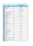
No 序号 1 2 3 4 5 6 7 8 9 10 11 12 13 14 15 16 17 18 19 20 21 22 23 灯具及灯具安装 Brake systems 制动 Tires 轮胎 Steering system displacement and impact 转向系统位移及碰撞 Steering system energy absorption 转向系统能量吸收 Seat strength and anchorages 座椅强度及固定点 Fuel system integrity 邮箱及燃油系统 Flammability of interior material 内饰材料可燃性 Head restrains 头枕 Seat belt installing 安全带及安装 Seat belt anchorage 安全带固定点 Windshield wiper/ washer defogging 雨刮洗涤剂 Rear view mirrors 后视镜 Audible warning 喇叭 Safty glass ( glazing) 安全玻璃 Transmission manul and automatic 手动挡和自动挡变速箱 Solar glare reflecting surfaces 表面非耀眼材质 Battery quick disconnect 蓄电池漏电保护 Door latches and hings 门锁及门铰链 Hood latch 发动机罩锁 Instrument panel identification of control 操纵件系统 Power windows , roof and interior divider 电动玻璃,天窗及内部分配器 Fire extinguisher Subject 项目 Lighting&installation Brazil Standard NO. 巴西标准号 227/07 294/08 777/933312/09( ABS ) 558/80RTQ 41(INMETRO) 463/73-4 463/73-7 463-3/73; 220/07 463-13/73; 486/75; 221/07 675/86 44/98; 220/07 48/98 48/99 224/07 226/07 035/98 254/07 461/72 463/73-2(提供法规) NA 463/73-11 461/72-F 225/07 649/85762/92 157/04,223/07 and 272/08
ASTM标准
ASTM"American Society for Testing and Materials"系美国材料与试验协会的英文缩写。
该技术协会成立于1898年。
ASTM标准制定一直采用自愿达成一致意见的制度。
标准制度由技术委员会负责,由标准工作组起草。
经过技术分委员会和技术委员会投票表决,在采纳大多数会员共同意见后,并由大多数会员投票赞成,标准才获批准,作为正式标准出版。
在一项标准编制过程中,对该编制感兴趣的每个会员和任何热心的团体都有权充分发表意见,委员会对提出的意见都给予研究和处理,以吸收各方面的正确意见和建议。
ASTM标准现分为15类(Section),各类所包含的卷数不同,标准分卷(Volume)出版,以ASTM标准年鉴形式出版发行。
第一类钢铁产品第二类有色金属第三类金属材料试验方法及分析程序第四类建设材料第五类石油产品、润滑剂及矿物燃料第六类油漆、相关涂料和芳香族化合物第七类纺织品及材料第八类塑料第九类橡胶第十类电气绝缘体和电子产品第十一类水和环境技术第十二类核能,太阳能第十三类医疗设备和服务第十四类仪器仪表及一般试验方法第十五类通用工业产品、特殊化学制品和消耗材料ASTM活动范围很广,形式多种多样。
它除出版各种标准资料外还办有期刊。
对ASTM标准的了解是美国试验与材料学会国际组织制定的标准,成立于1898年的ASTM International是世界上最大的制定自愿性标准的组织。
作为非赢利组织,ASTM lnternational为材料、产品.系统和服务的自愿性协商一致标准的制定和发布提供论坛。
ASTM lnternational的成员来自世界100多个国家,代表制造商、用户、消费者、政府和学术机构制定技术文件,这些技术文件是生产、管理、采购、以及制定法规与条例的基础。
这些成员隶属于一个或多个委员会,每个委员会负责某个领域的项目,例如钢铁、石油、医疗器材、财产管理、消费产品以及许多其他标准。
Ti(德州仪器)-芯片手册-sn74ac86

PACKAGING INFORMATIONAddendum-Page 1(1) The marketing status values are defined as follows:ACTIVE: Product device recommended for new designs.LIFEBUY: TI has announced that the device will be discontinued, and a lifetime-buy period is in effect.NRND: Not recommended for new designs. Device is in production to support existing customers, but TI does not recommend using this part in a new design.PREVIEW: Device has been announced but is not in production. Samples may or may not be available.OBSOLETE: TI has discontinued the production of the device.(2) Eco Plan - The planned eco-friendly classification: Pb-Free (RoHS), Pb-Free (RoHS Exempt), or Green (RoHS & no Sb/Br) - please check /productcontent for the latest availability information and additional product content details.TBD: The Pb-Free/Green conversion plan has not been defined.Pb-Free (RoHS): TI's terms "Lead-Free" or "Pb-Free" mean semiconductor products that are compatible with the current RoHS requirements for all 6 substances, including the requirement that lead not exceed 0.1% by weight in homogeneous materials. Where designed to be soldered at high temperatures, TI Pb-Free products are suitable for use in specified lead-free processes.Pb-Free (RoHS Exempt): This component has a RoHS exemption for either 1) lead-based flip-chip solder bumps used between the die and package, or 2) lead-based die adhesive used between the die and leadframe. The component is otherwise considered Pb-Free (RoHS compatible) as defined above.Green (RoHS & no Sb/Br): TI defines "Green" to mean Pb-Free (RoHS compatible), and free of Bromine (Br) and Antimony (Sb) based flame retardants (Br or Sb do not exceed 0.1% by weight in homogeneous material)(3) MSL, Peak Temp. - The Moisture Sensitivity Level rating according to the JEDEC industry standard classifications, and peak solder temperature.(4) There may be additional marking, which relates to the logo, the lot trace code information, or the environmental category on the device.(5) Multiple Device Markings will be inside parentheses. Only one Device Marking contained in parentheses and separated by a "~" will appear on a device. If a line is indented then it is a continuation of the previous line and the two combined represent the entire Device Marking for that device.Addendum-Page 2(6) Lead/Ball Finish - Orderable Devices may have multiple material finish options. Finish options are separated by a vertical ruled line. Lead/Ball Finish values may wrap to two lines if the finish value exceeds the maximum column width.Important Information and Disclaimer:The information provided on this page represents TI's knowledge and belief as of the date that it is provided. TI bases its knowledge and belief on information provided by third parties, and makes no representation or warranty as to the accuracy of such information. Efforts are underway to better integrate information from third parties. TI has taken and continues to take reasonable steps to provide representative and accurate information but may not have conducted destructive testing or chemical analysis on incoming materials and chemicals. TI and TI suppliers consider certain information to be proprietary, and thus CAS numbers and other limited information may not be available for release.In no event shall TI's liability arising out of such information exceed the total purchase price of the TI part(s) at issue in this document sold by TI to Customer on an annual basis.OTHER QUALIFIED VERSIONS OF SN54AC86, SN74AC86 :•Catalog: SN74AC86•Military: SN54AC86NOTE: Qualified Version Definitions:•Catalog - TI's standard catalog product•Military - QML certified for Military and Defense ApplicationsAddendum-Page 3TAPE AND REEL INFORMATION*All dimensions are nominalDevicePackage Type Package Drawing Pins SPQReel Diameter (mm)Reel Width W1(mm)A0(mm)B0(mm)K0(mm)P1(mm)W (mm)Pin1Quadrant SN74AC86DBR SSOP DB 142000330.016.48.2 6.6 2.512.016.0Q1SN74AC86DR SOIC D 142500330.016.4 6.59.0 2.18.016.0Q1SN74AC86NSR SO NS 142000330.016.48.210.5 2.512.016.0Q1SN74AC86PWRTSSOPPW142000330.012.46.95.61.68.012.0Q1*All dimensions are nominalDevice Package Type Package Drawing Pins SPQ Length(mm)Width(mm)Height(mm) SN74AC86DBR SSOP DB142000367.0367.038.0 SN74AC86DR SOIC D142500367.0367.038.0 SN74AC86NSR SO NS142000367.0367.038.0SN74AC86PWR TSSOP PW142000367.0367.035.0PACKAGE OUTLINECDIP - 5.08 mm max heightJ0014A CERAMIC DUAL IN LINE PACKAGENOTES:1. All controlling linear dimensions are in inches. Dimensions in brackets are in millimeters. Any dimension in brackets or parenthesis are for reference only. Dimensioning and tolerancing per ASME Y14.5M.2. This drawing is subject to change without notice.3. This package is hermitically sealed with a ceramic lid using glass frit.4. Index point is provided on cap for terminal identification only and on press ceramic glass frit seal only.5. Falls within MIL-STD-1835 and GDIP1-T14.EXAMPLE BOARD LAYOUTCDIP - 5.08 mm max heightJ0014A CERAMIC DUAL IN LINE PACKAGEIMPORTANT NOTICETexas Instruments Incorporated(TI)reserves the right to make corrections,enhancements,improvements and other changes to its semiconductor products and services per JESD46,latest issue,and to discontinue any product or service per JESD48,latest issue.Buyers should obtain the latest relevant information before placing orders and should verify that such information is current and complete.TI’s published terms of sale for semiconductor products(/sc/docs/stdterms.htm)apply to the sale of packaged integrated circuit products that TI has qualified and released to market.Additional terms may apply to the use or sale of other types of TI products and services.Reproduction of significant portions of TI information in TI data sheets is permissible only if reproduction is without alteration and is accompanied by all associated warranties,conditions,limitations,and notices.TI is not responsible or liable for such reproduced rmation of third parties may be subject to additional restrictions.Resale of TI products or services with statements different from or beyond the parameters stated by TI for that product or service voids all express and any implied warranties for the associated TI product or service and is an unfair and deceptive business practice.TI is not responsible or liable for any such statements. Buyers and others who are developing systems that incorporate TI products(collectively,“Designers”)understand and agree that Designers remain responsible for using their independent analysis,evaluation and judgment in designing their applications and that Designers have full and exclusive responsibility to assure the safety of Designers'applications and compliance of their applications(and of all TI products used in or for Designers’applications)with all applicable regulations,laws and other applicable requirements.Designer represents that,with respect to their applications,Designer has all the necessary expertise to create and implement safeguards that(1)anticipate dangerous consequences of failures,(2)monitor failures and their consequences,and(3)lessen the likelihood of failures that might cause harm and take appropriate actions.Designer agrees that prior to using or distributing any applications that include TI products,Designer will thoroughly test such applications and the functionality of such TI products as used in such applications.TI’s provision of technical,application or other design advice,quality characterization,reliability data or other services or information, including,but not limited to,reference designs and materials relating to evaluation modules,(collectively,“TI Resources”)are intended to assist designers who are developing applications that incorporate TI products;by downloading,accessing or using TI Resources in any way,Designer(individually or,if Designer is acting on behalf of a company,Designer’s company)agrees to use any particular TI Resource solely for this purpose and subject to the terms of this Notice.TI’s provision of TI Resources does not expand or otherwise alter TI’s applicable published warranties or warranty disclaimers for TI products,and no additional obligations or liabilities arise from TI providing such TI Resources.TI reserves the right to make corrections, enhancements,improvements and other changes to its TI Resources.TI has not conducted any testing other than that specifically described in the published documentation for a particular TI Resource.Designer is authorized to use,copy and modify any individual TI Resource only in connection with the development of applications that include the TI product(s)identified in such TI Resource.NO OTHER LICENSE,EXPRESS OR IMPLIED,BY ESTOPPEL OR OTHERWISE TO ANY OTHER TI INTELLECTUAL PROPERTY RIGHT,AND NO LICENSE TO ANY TECHNOLOGY OR INTELLECTUAL PROPERTY RIGHT OF TI OR ANY THIRD PARTY IS GRANTED HEREIN,including but not limited to any patent right,copyright,mask work right,or other intellectual property right relating to any combination,machine,or process in which TI products or services are rmation regarding or referencing third-party products or services does not constitute a license to use such products or services,or a warranty or endorsement e of TI Resources may require a license from a third party under the patents or other intellectual property of the third party,or a license from TI under the patents or other intellectual property of TI.TI RESOURCES ARE PROVIDED“AS IS”AND WITH ALL FAULTS.TI DISCLAIMS ALL OTHER WARRANTIES OR REPRESENTATIONS,EXPRESS OR IMPLIED,REGARDING RESOURCES OR USE THEREOF,INCLUDING BUT NOT LIMITED TO ACCURACY OR COMPLETENESS,TITLE,ANY EPIDEMIC FAILURE WARRANTY AND ANY IMPLIED WARRANTIES OF MERCHANTABILITY,FITNESS FOR A PARTICULAR PURPOSE,AND NON-INFRINGEMENT OF ANY THIRD PARTY INTELLECTUAL PROPERTY RIGHTS.TI SHALL NOT BE LIABLE FOR AND SHALL NOT DEFEND OR INDEMNIFY DESIGNER AGAINST ANY CLAIM, INCLUDING BUT NOT LIMITED TO ANY INFRINGEMENT CLAIM THAT RELATES TO OR IS BASED ON ANY COMBINATION OF PRODUCTS EVEN IF DESCRIBED IN TI RESOURCES OR OTHERWISE.IN NO EVENT SHALL TI BE LIABLE FOR ANY ACTUAL, DIRECT,SPECIAL,COLLATERAL,INDIRECT,PUNITIVE,INCIDENTAL,CONSEQUENTIAL OR EXEMPLARY DAMAGES IN CONNECTION WITH OR ARISING OUT OF TI RESOURCES OR USE THEREOF,AND REGARDLESS OF WHETHER TI HAS BEEN ADVISED OF THE POSSIBILITY OF SUCH DAMAGES.Unless TI has explicitly designated an individual product as meeting the requirements of a particular industry standard(e.g.,ISO/TS16949 and ISO26262),TI is not responsible for any failure to meet such industry standard requirements.Where TI specifically promotes products as facilitating functional safety or as compliant with industry functional safety standards,such products are intended to help enable customers to design and create their own applications that meet applicable functional safety standards and ing products in an application does not by itself establish any safety features in the application.Designers must ensure compliance with safety-related requirements and standards applicable to their applications.Designer may not use any TI products in life-critical medical equipment unless authorized officers of the parties have executed a special contract specifically governing such use. Life-critical medical equipment is medical equipment where failure of such equipment would cause serious bodily injury or death(e.g.,life support,pacemakers,defibrillators,heart pumps,neurostimulators,and implantables).Such equipment includes,without limitation,all medical devices identified by the U.S.Food and Drug Administration as Class III devices and equivalent classifications outside the U.S.TI may expressly designate certain products as completing a particular qualification(e.g.,Q100,Military Grade,or Enhanced Product). Designers agree that it has the necessary expertise to select the product with the appropriate qualification designation for their applications and that proper product selection is at Designers’own risk.Designers are solely responsible for compliance with all legal and regulatory requirements in connection with such selection.Designer will fully indemnify TI and its representatives against any damages,costs,losses,and/or liabilities arising out of Designer’s non-compliance with the terms and provisions of this Notice.Mailing Address:Texas Instruments,Post Office Box655303,Dallas,Texas75265Copyright©2017,Texas Instruments Incorporated。
74ACT00MTC中文资料
Device also available in Tape and Reel. Specify by appending suffix letter “X” to the ordering form. (PC not available in Tape and Reel.)
SN74LS86中文资料

LOW POWER SCHOTTKYDevice Package Shipping SN74LS86N 14 Pin DIP 2000 Units/Box SN74LS86D14 PinSOIC D SUFFIX CASE 751A2500/T ape & ReelPLASTIC N SUFFIX CASE 646141141ON Semiconductor and are trademarks of Semiconductor Components Industries, LLC (SCILLC). SCILLC reserves the right to make changes without further notice to any products herein. SCILLC makes no warranty, representation or guarantee regarding the suitability of its products for any particular purpose, nor does SCILLC assume any liability arising out of the application or use of any product or circuit, and specifically disclaims any and all liability, including without limitation special, consequential or incidental damages. “Typical” parameters which may be provided in SCILLC data sheets and/or specifications can and do vary in different applications and actual performance may vary over time. All operating parameters, including “Typicals” must be validated for each customer application by customer’s technical experts. SCILLC does not convey any license under its patent rights nor the rights of others.SCILLC products are not designed, intended, or authorized for use as components in systems intended for surgical implant into the body, or other applications intended to support or sustain life, or for any other application in which the failure of the SCILLC product could create a situation where personal injury or death may occur. Should Buyer purchase or use SCILLC products for any such unintended or unauthorized application, Buyer shall indemnify and hold SCILLC and its officers, employees, subsidiaries, affiliates, and distributors harmless against all claims, costs, damages, and expenses, and reasonable attorney fees arising out of, directly or indirectly, any claim of personal injury or death associated with such unintended or unauthorized use, even if such claim alleges that SCILLC was negligent regarding the design or manufacture of the part. SCILLC is an Equal Opportunity/Affirmative Action Employer. PUBLICATION ORDERING INFORMATIONASIA/PACIFIC: LDC for ON Semiconductor – Asia SupportPhone:303–675–2121 (Tue–Fri 9:00am to 1:00pm, Hong Kong Time)Toll Free from Hong Kong 800–4422–3781Email: ONlit–asia@JAPAN: ON Semiconductor, Japan Customer Focus Center4–32–1 Nishi–Gotanda, Shinagawa–ku, Tokyo, Japan 141–8549Phone: 81–3–5487–8345Email: r14153@Fax Response Line:303–675–2167。
74ls86中文资料_数据手册_参数
Singapore 049318
Harbour City, Canton Road, Tsim Sha Tsui,
Tel: 535-2100
Kowloon, Hong Kong
Fax: 535-1533
Tel: <852> (2) 735 9218
Fax: <852> (2) 730 0281
Hitachi Asia Ltd.
Hitachi Europe GmbH Electronic components Group Dornacher Stra§e 3 D-85622 Feldkirchen, Munich Germany Tel: <49> (89) 9 9180-0 Fax: <49> (89) 9 29 30 00
DP-14 Conforms Conforms 0.97 g
10.06 10.5 Max
14
8
5.5
1
7
1.42 Max
0.10 ± 0.10
1.27
*0.42 ± 0.08 0.40 ± 0.06
0.15 0.12 M
*Dimension including the plating thickness Base material dimension
For further information write to:
74ACT541_01中文资料

1/9April 2001s HIGH SPEED: t PD = 4ns (TYP .) at V CC = 5V sLOW POWER DISSIPATION:I CC = 4µA(MAX.) at T A =25°CsCOMPATIBLE WITH TTL OUTPUTS V IH = 2V (MIN.), V IL = 0.8V (MAX.)s50Ω TRANSMISSION LINE DRIVING CAPABILITYsSYMMETRICAL OUTPUT IMPEDANCE:|I OH | = I OL = 24mA (MIN)sBALANCED PROPAGATION DELAYS:t PLH ≅ t PHLsOPERATING VOLTAGE RANGE:V CC (OPR) = 4.5V to 5.5VsPIN AND FUNCTION COMPATIBLE WITH 74 SERIES 541sIMPROVED LATCH-UP IMMUNITYDESCRIPTIONThe 74ACT541 is an advanced high-speed CMOS OCTAL BUS BUFFER (3-STATE) fabricated with sub-micron silicon gate and double-layer metal wiring C 2MOS tecnology.The 3 STATE control gate operates as two input AND such that if either G1 and G2 are high, all eight outputs are in the high impedance state.In order to enhance PC board layout, the74ACT541 offers a pinout having inputs and outputs on opposite sides of the package.This device is designed to interface directly High Speed CMOS systems with TTL, NMOS and CMOS output voltage levlels.All inputs and outputs are equipped with protection circuits against static discharge, giving them 2KV ESD immunity and transient excess voltage.74ACT541OCTAL BUS BUFFERWITH 3 STATE OUTPUTS (NON INVERTED)PIN CONNECTION AND IEC LOGIC SYMBOLSORDER CODESPACKAGE TUBE T & R DIP 74ACT541B SOP 74ACT541M74ACT541MTR TSSOP74ACT541TTR74ACT5412/9INPUT AND OUTPUT EQUIVALENT CIRCUITPIN DESCRIPTIONTRUTH TABLEX : Don’t CareZ : High ImpedanceABSOLUTE MAXIMUM RATINGSAbsolute Maximum Ratings are those values beyond which damage to the device may occur. Functional operation under these conditions is not implied.RECOMMENDED OPERATING CONDITIONS1) V IN from 0.8V to 2.0VPIN No SYMBOL NAME AND FUNCTION 1, 19G1, G2Output Enable Inputs 2, 3, 4, 5, 6, 7, 8, 9A1 to A8Data Inputs 18, 17, 16, 15, 14, 13, 12, 11Y1 to Y8Data Outputs10GND Ground (0V)20V CCPositive Supply VoltageINPUTSOUTPUTG1G2An Yn H X X Z X H X Z L L H H LLLLSymbol ParameterValue Unit V CC Supply Voltage -0.5 to +7V V I DC Input Voltage -0.5 to V CC + 0.5V V O DC Output Voltage -0.5 to V CC + 0.5V I IK DC Input Diode Current ± 20mA I OK DC Output Diode Current ± 20mA I ODC Output Current± 50mA I CC or I GND DC V CC or Ground Current± 400mA T stg Storage Temperature-65 to +150°C T LLead Temperature (10 sec)300°CSymbol ParameterValue Unit V CC Supply Voltage 4.5 to 5.5V V I Input Voltage 0 to V CC V V O Output Voltage 0 to V CC V T op Operating Temperature-55 to 125°C dt/dvInput Rise and Fall Time V CC = 4.5 to 5.5V (note 1)8ns/V74ACT5413/9DC SPECIFICATIONS1) Maximum test duration 2ms, one output loaded at time2) Incident wave switching is guaranteed on transmission lines with impedances as low as 50ΩAC ELECTRICAL CHARACTERISTICS (C L = 50 pF, R L = 500 Ω, Input t r = t f = 3ns)(*) Voltage range is 5.0V ± 0.5VSymbolParameterTest ConditionValue UnitV CC (V)T A = 25°C -40 to 85°C -55 to 125°C Min.Typ.Max.Min.Max.Min.Max.V IH High Level Input Voltage4.5V O = 0.1 V or V CC -0.1V 2.0 1.5 2.0 2.0V5.5 2.01.52.02.0V IL Low Level Input Voltage4.5V O = 0.1 V or V CC -0.1V 1.50.80.80.85.5 1.50.80.80.8VV OHHigh Level Output Voltage4.5I O =-50 µA 4.4 4.49 4.4 4.45.5I O =-50 µA 5.4 5.495.4 5.44.5I O =-24 mA 3.86 3.76 3.7V5.5I O =-24 mA 4.864.764.7V OLLow Level Output Voltage4.5I O =50 µA 0.0010.10.10.15.5I O =50 µA 0.0010.10.10.14.5I O =24 mA 0.360.440.55.5I O =24 mA 0.360.440.5I I Input Leakage Cur-rent5.5V I = V CC or GND ± 0.1± 1± 1µA I OZ High Impedance Output Leakege Current5.5V I = V IH or V IL V O = V CC or GND ± 0.5± 5± 5µA I CCT Max I CC /Input 5.5V I = V CC - 2.1V 0.61.5 1.6mA I CC Quiescent Supply Current5.5V I = V CC or GND 44080µA I OLD Dynamic Output Current (note 1, 2)5.5V OLD = 1.65 V max 7550mA I OHDV OHD = 3.85 V min-75-50mA SymbolParameterTest ConditionValue UnitV CC (V)T A = 25°C -40 to 85°C -55 to 125°C Min.Typ.Max.Min.Max.Min.Max.t PLH t PHL Propagation DelayTime5.0(*) 1.5 4.06.5 1.58.0 1.58.0ns t PZL t PZH Output EnableTime5.0(*) 1.56.07.8 1.59.0 1.59.0ns t PLZ t PHZ Output DisableTime5.0(*)1.55.07.81.59.01.59.0ns74ACT5414/9CAPACITIVE CHARACTERISTICSPD load. (Refer to Test Circuit). Average operating current can be obtained by the following equation. I CC(opr) = C PD x V CC x f IN + I CC /n (per circuit)TEST CIRCUITC L = 50pF or equivalent (includes jig and probe capacitance)R L = R 1 = 500Ω or equivalentR T = Z OUT of pulse generator (typically 50Ω)SymbolParameterTest ConditionValue UnitV CC (V)T A = 25°C -40 to 85°C -55 to 125°C Min.Typ.Max.Min.Max.Min.Max.C IN Input Capacitance 5.04pF C OUT OutputCapacitance5.08pF C PDPower Dissipation Capacitance (note 1)5.0f IN = 10MHz22pF TESTSWITCH t PLH , t PHL Open t PZL , t PLZ 2V CC t PZH , t PHZOpen74ACT5415/9WAVEFORM 1: PROPAGATION DELAYS (f=1MHz; 50% duty cycle)WAVEFORM 2: OUTPUT ENABLE AND DISABLE TIME(f=1MHz; 50% duty cycle)74ACT541 Information furnished is believed to be accurate and reliable. However, STMicroelectronics assumes no responsibility for the consequences of use of such information nor for any infringement of patents or other rights of third parties which may result from its use. No license is granted by implication or otherwise under any patent or patent rights of STMicroelectronics. Specifications mentioned in this publication are subject to change without notice. This publication supersedes and replaces all information previously supplied. STMicroelectronics products are not authorized for use as critical components in life support devices or systems without express written approval of STMicroelectronics.© The ST logo is a registered trademark of STMicroelectronics© 2001 STMicroelectronics - Printed in Italy - All Rights ReservedSTMicroelectronics GROUP OF COMPANIESAustralia - Brazil - China - Finland - France - Germany - Hong Kong - India - Italy - Japan - Malaysia - Malta - MoroccoSingapore - Spain - Sweden - Switzerland - United Kingdom© 9/9。
常用74系列芯片

74系列集成电路大全74系列集成电路大致可分为6大类:74××(标准型);74LS××(低功耗肖特基);74S××(肖特基);74ALS××(先进低功耗肖特基);74AS××(先进肖特基);74F××(高速)。
HC为COMS工作电平;HCT为TTL工作电平,可与74LS系列互换使用;HCU适用于无缓冲级的CMOS电路。
这9种74系列产品,只要后边的标号相同,其逻辑功能和管脚排列就相同。
根据不同的条件和要求可选择不同类型的74系列产品,比如电路的供电电压为3V就应选择74HC系列的产品。
补充:.74 –系列这是早期的产品,现仍在使用,但正逐渐被淘汰。
2.74H –系列这是74 –系列的改进型,属于高速TTL产品。
其“与非门”的平均传输时间达10ns左右,但电路的静态功耗较大,目前该系列产品使用越来越少,逐渐被淘汰。
3.74S –系列这是TTL的高速型肖特基系列。
在该系列中,采用了抗饱和肖特基二极管,速度较高,但品种较少。
4.74LS –系列这是当前TTL类型中的主要产品系列。
品种和生产厂家都非常多。
性能价格比比较高,目前在中小规模电路中应用非常普遍。
5.74ALS –系列这是“先进的低功耗肖特基”系列。
属于74LS –系列的后继产品,速度(典型值为4ns)、功耗(典型值为1mW)等方面都有较大的改进,但价格比较高。
6.74AS –系列这是74S –系列的后继产品,尤其速度(典型值为1.5ns)有显著的提高,又称“先进超高速肖特基”系列。
7.74HC –系列54/74HC –系列是高速CMOS标准逻辑电路系列,具有与74LS –系列同等的工作度和CMOS集成电路固有的低功耗及电源电压范围宽等特点。
74HCxxx是74LSxxx同序号的翻版,型号最后几位数字相同,表示电路的逻辑功能、管脚排列完全兼容,为用74HC替代74LS提供了方便。
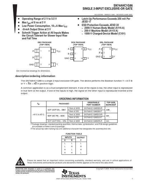
SN74AHC1G86_08中文资料
PACKAGING INFORMATIONOrderable Device Status(1)PackageType PackageDrawingPins PackageQtyEco Plan(2)Lead/Ball Finish MSL Peak Temp(3)SN74AHC1G86DBVG4ACTIVE SOT-23DBV5TBD Call TI Call TISN74AHC1G86DBVR ACTIVE SOT-23DBV53000Green(RoHS&no Sb/Br)CU NIPDAU Level-1-260C-UNLIMSN74AHC1G86DBVRE4ACTIVE SOT-23DBV53000Green(RoHS&no Sb/Br)CU NIPDAU Level-1-260C-UNLIMSN74AHC1G86DBVRG4ACTIVE SOT-23DBV53000Green(RoHS&no Sb/Br)CU NIPDAU Level-1-260C-UNLIMSN74AHC1G86DBVT ACTIVE SOT-23DBV5250Green(RoHS&no Sb/Br)CU NIPDAU Level-1-260C-UNLIMSN74AHC1G86DBVTE4ACTIVE SOT-23DBV5250Green(RoHS&no Sb/Br)CU NIPDAU Level-1-260C-UNLIMSN74AHC1G86DBVTG4ACTIVE SOT-23DBV5250Green(RoHS&no Sb/Br)CU NIPDAU Level-1-260C-UNLIMSN74AHC1G86DCKR ACTIVE SC70DCK53000Green(RoHS&no Sb/Br)CU NIPDAU Level-1-260C-UNLIMSN74AHC1G86DCKRE4ACTIVE SC70DCK53000Green(RoHS&no Sb/Br)CU NIPDAU Level-1-260C-UNLIMSN74AHC1G86DCKRG4ACTIVE SC70DCK53000Green(RoHS&no Sb/Br)CU NIPDAU Level-1-260C-UNLIMSN74AHC1G86DCKT ACTIVE SC70DCK5250Green(RoHS&no Sb/Br)CU NIPDAU Level-1-260C-UNLIMSN74AHC1G86DCKTE4ACTIVE SC70DCK5250Green(RoHS&no Sb/Br)CU NIPDAU Level-1-260C-UNLIMSN74AHC1G86DCKTG4ACTIVE SC70DCK5250Green(RoHS&no Sb/Br)CU NIPDAU Level-1-260C-UNLIMSN74AHC1G86DRLR ACTIVE SOT DRL54000Green(RoHS&no Sb/Br)CU NIPDAU Level-1-260C-UNLIMSN74AHC1G86DRLRG4ACTIVE SOT DRL54000Green(RoHS&no Sb/Br)CU NIPDAU Level-1-260C-UNLIM(1)The marketing status values are defined as follows:ACTIVE:Product device recommended for new designs.LIFEBUY:TI has announced that the device will be discontinued,and a lifetime-buy period is in effect.NRND:Not recommended for new designs.Device is in production to support existing customers,but TI does not recommend using this part in a new design.PREVIEW:Device has been announced but is not in production.Samples may or may not be available.OBSOLETE:TI has discontinued the production of the device.(2)Eco Plan-The planned eco-friendly classification:Pb-Free(RoHS),Pb-Free(RoHS Exempt),or Green(RoHS&no Sb/Br)-please check /productcontent for the latest availability information and additional product content details.TBD:The Pb-Free/Green conversion plan has not been defined.Pb-Free(RoHS):TI's terms"Lead-Free"or"Pb-Free"mean semiconductor products that are compatible with the current RoHS requirements for all6substances,including the requirement that lead not exceed0.1%by weight in homogeneous materials.Where designed to be soldered at high temperatures,TI Pb-Free products are suitable for use in specified lead-free processes.Pb-Free(RoHS Exempt):This component has a RoHS exemption for either1)lead-based flip-chip solder bumps used between the die and package,or2)lead-based die adhesive used between the die and leadframe.The component is otherwise considered Pb-Free(RoHS compatible)as defined above.Green(RoHS&no Sb/Br):TI defines"Green"to mean Pb-Free(RoHS compatible),and free of Bromine(Br)and Antimony(Sb)based flame retardants(Br or Sb do not exceed0.1%by weight in homogeneous material)(3)MSL,Peak Temp.--The Moisture Sensitivity Level rating according to the JEDEC industry standard classifications,and peak solder temperature.Important Information and Disclaimer:The information provided on this page represents TI's knowledge and belief as of the date that it is provided.TI bases its knowledge and belief on information provided by third parties,and makes no representation or warranty as to the accuracy of such information.Efforts are underway to better integrate information from third parties.TI has taken and continues to take reasonable steps to provide representative and accurate information but may not have conducted destructive testing or chemical analysis on incoming materials and chemicals.TI and TI suppliers consider certain information to be proprietary,and thus CAS numbers and other limited information may not be available for release.In no event shall TI's liability arising out of such information exceed the total purchase price of the TI part(s)at issue in this document sold by TI to Customer on an annual basis.TAPE AND REEL INFORMATION*All dimensions are nominalDevicePackage Type Package Drawing Pins SPQReel Diameter (mm)Reel Width W1(mm)A0(mm)B0(mm)K0(mm)P1(mm)W (mm)Pin1Quadrant SN74AHC1G86DBVR SOT-23DBV 53000178.09.0 3.23 3.17 1.37 4.08.0Q3SN74AHC1G86DBVR SOT-23DBV 53000180.09.2 3.23 3.17 1.37 4.08.0Q3SN74AHC1G86DBVT SOT-23DBV 5250180.09.2 3.23 3.17 1.37 4.08.0Q3SN74AHC1G86DCKR SC70DCK 53000180.09.2 2.24 2.34 1.22 4.08.0Q3SN74AHC1G86DCKR SC70DCK 53000178.09.0 2.4 2.5 1.2 4.08.0Q3SN74AHC1G86DCKT SC70DCK 5250178.09.0 2.4 2.5 1.2 4.08.0Q3SN74AHC1G86DCKT SC70DCK 5250180.09.2 2.24 2.34 1.22 4.08.0Q3SN74AHC1G86DRLRSOTDRL54000180.09.21.781.780.694.08.0Q3*All dimensions are nominalDevice Package Type Package Drawing Pins SPQ Length(mm)Width(mm)Height(mm) SN74AHC1G86DBVR SOT-23DBV53000180.0180.018.0 SN74AHC1G86DBVR SOT-23DBV53000202.0201.028.0 SN74AHC1G86DBVT SOT-23DBV5250202.0201.028.0 SN74AHC1G86DCKR SC70DCK53000202.0201.028.0 SN74AHC1G86DCKR SC70DCK53000180.0180.018.0 SN74AHC1G86DCKT SC70DCK5250180.0180.018.0 SN74AHC1G86DCKT SC70DCK5250202.0201.028.0 SN74AHC1G86DRLR SOT DRL54000202.0201.028.0IMPORTANT NOTICETexas Instruments Incorporated and its subsidiaries(TI)reserve the right to make corrections,modifications,enhancements,improvements, and other changes to its products and services at any time and to discontinue any product or service without notice.Customers should obtain the latest relevant information before placing orders and should verify that such information is current and complete.All products are sold subject to TI’s terms and conditions of sale supplied at the time of order acknowledgment.TI warrants performance of its hardware products to the specifications applicable at the time of sale in accordance with TI’s standard warranty.Testing and other quality control techniques are used to the extent TI deems necessary to support this warranty.Except where mandated by government requirements,testing of all parameters of each product is not necessarily performed.TI assumes no liability for applications assistance or customer product design.Customers are responsible for their products and applications using TI components.To minimize the risks associated with customer products and applications,customers should provide adequate design and operating safeguards.TI does not warrant or represent that any license,either express or implied,is granted under any TI patent right,copyright,mask work right, or other TI intellectual property right relating to any combination,machine,or process in which TI products or services are rmation published by TI regarding third-party products or services does not constitute a license from TI to use such products or services or a warranty or endorsement e of such information may require a license from a third party under the patents or other intellectual property of the third party,or a license from TI under the patents or other intellectual property of TI.Reproduction of TI information in TI data books or data sheets is permissible only if reproduction is without alteration and is accompanied by all associated warranties,conditions,limitations,and notices.Reproduction of this information with alteration is an unfair and deceptive business practice.TI is not responsible or liable for such altered rmation of third parties may be subject to additional restrictions.Resale of TI products or services with statements different from or beyond the parameters stated by TI for that product or service voids all express and any implied warranties for the associated TI product or service and is an unfair and deceptive business practice.TI is not responsible or liable for any such statements.TI products are not authorized for use in safety-critical applications(such as life support)where a failure of the TI product would reasonably be expected to cause severe personal injury or death,unless officers of the parties have executed an agreement specifically governing such use.Buyers represent that they have all necessary expertise in the safety and regulatory ramifications of their applications,and acknowledge and agree that they are solely responsible for all legal,regulatory and safety-related requirements concerning their products and any use of TI products in such safety-critical applications,notwithstanding any applications-related information or support that may be provided by TI.Further,Buyers must fully indemnify TI and its representatives against any damages arising out of the use of TI products in such safety-critical applications.TI products are neither designed nor intended for use in military/aerospace applications or environments unless the TI products are specifically designated by TI as military-grade or"enhanced plastic."Only products designated by TI as military-grade meet military specifications.Buyers acknowledge and agree that any such use of TI products which TI has not designated as military-grade is solely at the Buyer's risk,and that they are solely responsible for compliance with all legal and regulatory requirements in connection with such use. TI products are neither designed nor intended for use in automotive applications or environments unless the specific TI products are designated by TI as compliant with ISO/TS16949requirements.Buyers acknowledge and agree that,if they use any non-designated products in automotive applications,TI will not be responsible for any failure to meet such requirements.Following are URLs where you can obtain information on other Texas Instruments products and application solutions:Products ApplicationsAmplifiers AudioData Converters AutomotiveDSP BroadbandClocks and Timers Digital ControlInterface MedicalLogic MilitaryPower Mgmt Optical NetworkingMicrocontrollers SecurityRFID TelephonyRF/IF and ZigBee®Solutions Video&ImagingWirelessMailing Address:Texas Instruments,Post Office Box655303,Dallas,Texas75265Copyright©2008,Texas Instruments Incorporated。
海外汽车认证检测项目及法规列表(中英文)
灭火器 24 25 26 27 28 29 30 License plate 牌照板 Vehicle identification number VIN 码 Obligatory requirement 必要装置 Theft protection 防盗保护 Speedometers-odometers 速度仪 Reflective triangle warning device 三角警告装置 Image generator ( GPS AND DVD) Air bag 安全气囊 Protetion to passengers and criteria to biomecanica,frontal impact tests 乘员保护-前碰撞保护 Behavior of the vehicle structure to rear impact tests 车辆后碰撞保护 31 32 33 Exterior sound (noise) levels 车辆外部噪音 Diesel smoke 柴油烟度 Exhaust emission 排气污染物 34 EMC 电磁兼容
EEC指令或 ECE法规
√ — —
EEC指令或 ECE法规
√ பைடு நூலகம் —
ISO 362-1981(E),ISO 5130-1981(E)
√ √ √
依据不同测试循环,应该在巴西检测,被 √ √ √ 批准的发动机除外。柴油为 50ppm of HC EURO Ⅳ :2009年 1月 1日 .M1及 N1类车: EPA-FTP √ √ √ 75.N2类车: OBDⅠ和Ⅱ .在巴西进行测试 巴西电信部检测
76/758/EEC
23 24 25
机动车辆及其挂车的示廓灯、前位置(侧)灯 、后位置(侧)灯、 制动灯、侧标志灯、白 日行驶灯 Direction indicators 机动车辆及其挂车的转向指示灯 Rear registration plate lamps 机动车辆及其挂车的后牌照灯 Headlamps (including bulbs) 机动车辆远光灯和/或近光前照灯以及这些 前照灯装用的白炽灯泡 Front fog lamps 机动车辆前雾灯及其所用的灯丝灯泡 Towing hooks 机动车辆牵引装置 Rear fog lamps 机动车辆及其挂车后雾灯 Reversing lamps 机动车辆及其挂车倒车灯 Parking lamps 机动车辆驻车灯 Seat belts and restraint systems 安全带部件及约束系统 Forward vision 机动车辆驾驶员视野 Identification of controls 机动车辆操纵件、信号装置和指示器的识别 Defrost/demist 机动车辆玻璃表面的除霜和除雾系统 Wash/wipe 机动车辆刮水器和清洗器系统 Heating systems 机动车辆及其挂车加热系统 Wheel guards 机动车辆护轮板 Head restraints 机动车辆座椅头枕 CO2 emissions/fuel consumption 机动车辆co2排放及燃油消耗 Engine power 机动车辆发动机功率 Diesel emissions 控制车用柴油机气体污染物排放的措施 Lateral protection 机动车辆及其挂车侧面防护 Spray-suppression systems 机动车辆及其挂车防飞溅系统 Masses and dimensions(cars) M1类机动车辆质量和尺寸 Safety glass 机动车辆及其挂车安全玻璃及玻璃材料 Tyres 机动车辆及其挂车轮胎及其安装 Speed limiters 限速装置或类似的车载限速系统
4 维修常用英语整合

Color Bar Test Fail
色度條紋不良
行地址鎖存 价值工程
Serial Port Clock
串口接口時鐘
維修常用英語
N0. 151 152 153 154 155 156 157 158 159 160 英文簡稱 SPI SCL SDA SK DI DO BCLK VLR When where Visitor Location Register 英文全名 中文 串行外圍設備接口 串行時鐘 串行數據 串行數據時鐘 串行數據輸入 串行數據輸出 位時鐘 位置訪問寄存器 何時做 何處做
Package Drawing
PCL PCs PDCA Cycle PEFIPH Plan POP POR POWCONTROL Power supply Plan Packing Operation Process Power Control Level Pieces
包裝圖面文件
功率控制等級 片 PDCA循環: 外圍設備 計划 包裝作業規范 上電復位 功率控制 電源
中文
Band8終端呼叫
USB數據處理
工作因素法 WI/BT/調頻收音機模 塊 工作评价与考核 工作測量 工作抽樣
工程管制系統
Engineering control system 四大管制系統
99
100
Manufacturing control system
Quality control system
維修常用英語
N0. 121 英文簡稱 AML 英文全名 Approved Manufactory List 中文 合格制造商
122
123 124 125 126 127 128
74ACT04中文资料
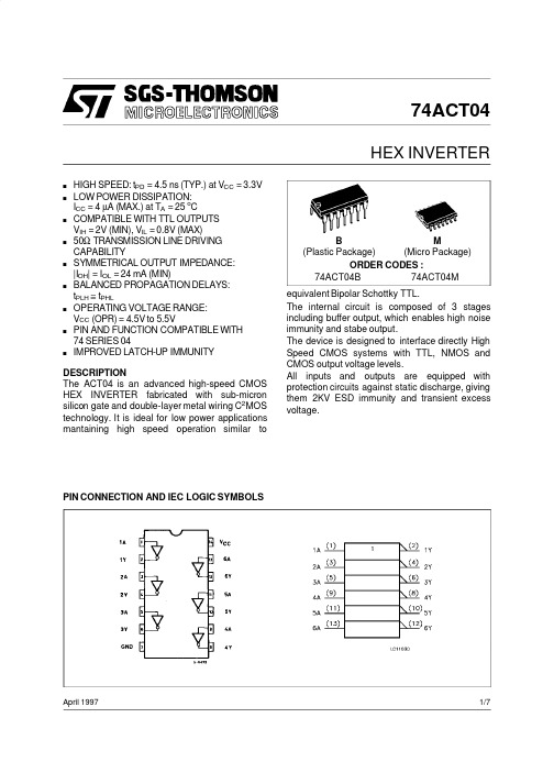
74ACT04HEX INVERTERApril 1997s HIGH SPEED:t PD =4.5ns (TYP.)at V CC =3.3V sLOW POWER DISSIPATION:I CC =4µA (MAX.)at T A =25o CsCOMPATIBLE WITH TTL OUTPUTS V IH =2V (MIN),V IL =0.8V (MAX)s50ΩTRANSMISSION LINE DRIVING CAPABILITYsSYMMETRICAL OUTPUT IMPEDANCE:|I OH |=I OL =24mA (MIN)sBALANCED PROPAGATION DELAYS:t PLH ≅t PHLsOPERATING VOLTAGE RANGE:V CC (OPR)=4.5V to 5.5VsPIN AND FUNCTION COMPATIBLE WITH 74SERIES 04sIMPROVED LATCH-UP IMMUNITYDESCRIPTIONThe ACT04is an advanced high-speed CMOS HEX INVERTER fabricated with sub-micron silicon gate and double-layer metal wiring C 2MOS technology.It is ideal for low power applications mantaining high speed operation similar toequivalent Bipolar Schottky TTL.The internal circuit is composed of 3stages including buffer output,which enables high noise immunity and stabe output.The device is designed to interface directly High Speed CMOS systems with TTL,NMOS and CMOS output voltage levels.All inputs and outputs are equipped with protection circuits against static discharge,giving them 2KV ESD immunity and transient excess voltage.PIN CONNECTION AND IEC LOGIC SYMBOLSORDER CODES :74ACT04B 74ACT04M M(Micro Package)B (Plastic Package)1/7INPUT AND OUTPUT EQUIVALENT CIRCUITABSOLUTE MAXIMUM RATINGSSymbol ParameterValue Unit V CC Supply Voltage -0.5to +7V V I DC Input Voltage -0.5to V CC +0.5V V O DC Output Voltage -0.5to V CC +0.5V I IK DC Input Diode Current ±20mA I OK DC Output Diode Current ±20mA I O DC Output Current ±50mA I CC or I GND DC V CC or Ground Current±300mAT stg Storage Temperature -65to +150o C T LLead Temperature (10sec)300oCAbsolute Maximum Ratings are those values beyond which damage to the device may occur.Functional operation under these condition is not implied.TRUTH TABLEA Y L H HLPIN DESCRIPTIONPIN No SYMBOL NAME AND FUNCTION 1,3,5,9,11,131A to 6A Data Inputs 2,4,6,8,10,121Y to 6Y Data Oututs 7GND Ground (0V)14V CCPositive Supply VoltageRECOMMENDED OPERATING CONDITIONSSymbol ParameterValue Unit V CC Supply Voltage 4.5to 5.5V V I Input Voltage 0to V CC V V O Output Voltage0to V CC VT op Operating Temperature:-40to +85oCdt/dvInput Rise and Fall Time V CC =4.5to 5.5V (note 1)8ns/V1)V IN from 0.8V to 2.0V74ACT042/7CAPACITIVE CHARACTERISTICSSymbolParameterTest ConditionsValueUnitV CC (V)T A =25oC -40to 85oC Min.Typ.Max.Min.Max.C IN Input Capacitance 5.04pF C PDPower Dissipation Capacitance (note 1)5.037pF1)C PD isdefined as the value of the IC’s internal equivalent capacitance which is calculated from the operating current consumption without load.(Refer to Test Circuit).Ave rage operating current can be obtained by the following equation.I CC (opr)=C PD •V CC •f IN +I CC /n (per circuit)AC ELECTRICAL CHARACTERISTICS (C L =50pF,R L =500Ω,Input t r =t f =3ns)SymbolParameterTest ConditionValueUnitV CC (V)T A =25oC -40to 85o CMin.Typ.Max.Min.Max.t PLH t PHLPropagation Delay Time5.0(*)1.5 4.57.5 1.08.5ns(*)Voltage range is 5V ±0.5VDC SPECIFICATIONSSymbolParameterTest ConditionsValueUnitV CC (V)T A =25oC -40to 85oC Min.Typ.Max.Min.Max.V IH High Level Input Voltage 4.5V O =0.1V or V CC -0.1V 2.0 1.5 2.0V 5.5 2.01.52.0V IL Low Level Input Voltage 4.5V O =0.1V or V CC -0.1V 1.50.80.8V 5.5 1.50.80.8V OHHigh Level Output Voltage4.5V I (*)=V IH or V ILI O =-50µA 4.4 4.49 4.4V5.5I O =-50µA 5.4 5.495.44.5I O =-24mA 3.86 3.765.5I O =-24mA 4.864.76V OLLow Level Output Voltage4.5V I (*)=V IH or V ILI O =50µA 0.0010.10.1V5.5I O =50mA 0.0010.10.14.5I O =24mA 0.360.445.5I O =24mA0.360.44I I Input Leakage Current 5.5V I =V CC or GND ±0.1±1µA I CCT Max I CC /Input 5.5V I =V CC -2.1V 0.61.5mA I CC Quiescent Supply Current5.5V I =V CC or GND 440mA I OLD Dynamic Output Current (note 1,2)5.5V OLD =1.65V max 75mA I OHDV OHD =3.85V min-75mA1)Maximum test duration 2ms,one output loaded at time2)Incident wave switch ing is guaranteed on transmission lines with impe dances as low as 50Ω.(*)All outputs loaded.74ACT043/774ACT04TEST CIRCUITC L=50pF or equivalent(includes jig and probe capacitance)R L=R1=500Ωor equiva lentR T=Z OUT of pulse generator(typically50Ω)WAVEFORM:PROPAGATION DELAYS(f=1MHz) 4/7DIM.mminch MIN.TYP.MAX.MIN.TYP.MAX.a10.510.020B 1.391.650.0550.065b 0.50.020b10.250.010D 200.787E 8.50.335e 2.540.100e315.240.600F 7.10.280I 5.10.201L 3.30.130Z1.272.540.0500.100P001APlastic DIP14MECHANICAL DATA74ACT045/7DIM.mm inch MIN.TYP.MAX.MIN.TYP.MAX.A 1.750.068a10.10.20.0030.007a2 1.650.064b 0.350.460.0130.018b10.190.250.0070.010C 0.50.019c145(typ.)D 8.558.750.3360.344E 5.86.20.2280.244e 1.270.050e37.620.300F 3.8 4.00.1490.157G 4.6 5.30.1810.208L 0.5 1.270.0190.050M 0.680.026S8(max.)P013GSO14MECHANICAL DATA74ACT046/774ACT04 Information furnished is believed to be accurate and reliable.However,SGS-THOMSON Microelectronics assumes no responsabilit y for the consequences of use of such information nor for any infringemen t of patents or other rights of third parties which may results from its use.No license is granted by implication or otherwise under any patent or patent rights of SGS-THOMSON Microelectr onics.Specifications mention ed in this publication are subject to change without notice.This publication supersede s and replaces all information previously supplied.SGS-THOMSON Microelectr onics products are not auth orized for use as critical compon ents in life support devices or systems without expre ss written approval of SGS-THOMSON Microelectonics.©1997SGS-THOMSON Microelectronics-Printed in Italy-All Rights Reserve dSGS-THOMSON Microelectronics GROUP OF COMPANIESAustralia-Brazil-Canada-China-France-Germany-Hong Kong-Italy-Japan-Korea-Malaysia-Malta-Morocco-The Netherlands-Singapore-Spain-Sweden-Switzerland-Taiwan-Thailand-United Kingdom-U.S.A.7/7。
74ACT32PC中文资料

元器件交易网
74AC32 • 74ACT32
Absolute Maximum Ratings(Note 1)
Supply Voltage (VCC) DC Input Diode Current (IIK) VI = −0.5V VI = VCC + 0.5V DC Input Voltage (VI) DC Output Diode Current (IOK) VO = −0.5V VO = VCC + 0.5V DC Output Voltage (VO) DC Output Source or Sink Current (IO) DC VCC or Ground Current per Output Pin (ICC or IGND) Storage Temperature (TSTG) Junction Temperature (TJ) PDIP 140°C ±50 mA −65°C to +150°C ±50 mA −20 mA +20 mA −0.5V to VCC + 0.5V −20 mA +20 mA −0.5V to VCC + 0.5V −0.5V to +7.0V
MC74ACT86DG,MC74AC86DR2G,MC74ACT86DR2G,MC74ACT86DR2G,MC74AC86DG,MC74AC86DTR2G, 规格书,Datasheet 资料

MC74AC86, MC74ACT86 Quad 2−Input Exclusive−OR GateFeatures•Outputs Source/Sink 24 mA•Pb−Free Packages are AvailableMAXIMUM RATINGSRating Symbol Value Unit DC Supply Voltage (Referenced to GND)V CC−0.5 to+7.0VDC Input Voltage (Referenced to GND)V in−0.5 toV CC +0.5VDC Output Voltage (Referenced to GND)V out−0.5 toV CC +0.5V DC Input Current, per Pin I in±20mA DC Output Sink/Source Current, per Pin I out±50mA DC V CC or GND Current per Output Pin I CC±50mAStorage Temperature T stg−65 to+150°CStresses exceeding Maximum Ratings may damage the device. Maximum Ratings are stress ratings only. Functional operation above the Recommended Operating Conditions is not implied. Extended exposure to stresses above the Recommended Operating Conditions may affect device reliability.See general marking information in the device marking section on page 5 of this data sheet.DEVICE MARKING INFORMATIONSee detailed ordering and shipping information in the package dimensions section on page 4 of this data sheet.ORDERING INFORMATION1314121110982134567GND V CCPinout: 14−Lead Packages Conductors(Top View)RECOMMENDED OPERATING CONDITIONSSymbol Parameter Min Typ Max UnitV CC Supply Voltage′AC 2.0 5.0 6.0V ′ACT 4.5 5.0 5.5V in, V out DC Input Voltage, Output Voltage (Ref. to GND)0V CC Vt r, t f Input Rise and Fall Time (Note 1)′AC Devices except Schmitt Inputs V CC @ 3.0 V−150−V CC @ 4.5 V−40−ns/V V CC @ 5.5 V−25−t r, t f Input Rise and Fall Time (Note 2)′ACT Devices except Schmitt Inputs V CC @ 4.5 V−10−ns/V V CC @ 5.5 V−8.0−T J Junction Temperature (PDIP)−−140°C T A Operating Ambient Temperature Range−402585°C I OH Output Current − High−−−24mAI OL Output Current − Low−−24mA1.V in from 30% to 70% V CC; see individual Data Sheets for devices that differ from the typical input rise and fall times.2.V in from 0.8 V to 2.0 V; see individual Data Sheets for devices that differ from the typical input rise and fall times.DC CHARACTERISTICSSymbol Parameter V CC(V)74AC74ACUnit Conditions T A = +25°CT A =−40°C to+85°CTyp Guaranteed LimitsV IH Minimum High LevelInput Voltage 3.0 1.5 2.1 2.1V OUT = 0.1 V4.5 2.25 3.15 3.15V or V CC− 0.1 V5.5 2.75 3.85 3.85V IL Maximum Low LevelInput Voltage 3.0 1.50.90.9V OUT = 0.1 V4.5 2.25 1.35 1.35V or V CC− 0.1 V5.5 2.75 1.65 1.65V OH Minimum High LevelOutput Voltage 3.0 2.99 2.9 2.9I OUT = −50 m A4.5 4.49 4.4 4.4V5.5 5.49 5.4 5.4V*V IN = V IL or V IH3.0− 2.56 2.46−12 mA4.5− 3.86 3.76I OH−24 mA5.5− 4.86 4.76−24 mAV OL Maximum Low LevelOutput Voltage 3.00.0020.10.1I OUT = 50 m A4.50.0010.10.1V5.50.0010.10.1V*V IN = V IL or V IH3.0−0.360.4412 mA4.5−0.360.44I OL24 mA5.5−0.360.4424 mAI IN Maximum InputLeakage Current 5.5−±0.1±1.0m A V I = V CC, GNDI OLD†Minimum DynamicOutput Current 5.5−−75mA V OLD = 1.65 V MaxI OHD 5.5−−−75mA V OHD = 3.85 V Min I CC Maximum QuiescentSupply Current 5.5− 4.040m A V IN = V CC or GND *All outputs loaded; thresholds on input associated with output under test.†Maximum test duration 2.0 ms, one output loaded at a time.NOTE:I IN and I CC @ 3.0 V are guaranteed to be less than or equal to the respective limit @ 5.5 V V CC.AC CHARACTERISTICS(For Figures and Waveforms − See Section 3 of the ON Semiconductor FACT Data Book, DL138/D)Symbol Parameter V CC*(V)74AC74ACUnitFig.No.T A = +25°CC L = 50 pFT A = −40°Cto +85°CC L = 50 pFMin Typ Max Min Maxt PLH Propagation DelayInputs to Outputs3.3 2.0 6.011.5 1.512.5ns3−55.0 1.5 4.58.5 1.09.0t PHL Propagation DelayInputs to Outputs3.3 2.0 6.511.5 1.512.5ns3−55.0 1.5 4.58.5 1.09.5*Voltage Range 3.3 V is 3.3 V ±0.3 V Voltage Range 5.0 V is 5.0 V ±0.5 V.DC CHARACTERISTICSSymbol Parameter V CC(V)74ACT74ACTUnit Conditions T A = +25°CT A =−40°C to+85°CTyp Guaranteed LimitsV IH Minimum High LevelInput Voltage 4.5 1.5 2.0 2.0VV OUT = 0.1 V 5.5 1.5 2.0 2.0or V CC− 0.1 VV IL Maximum Low LevelInput Voltage 4.5 1.50.80.8VV OUT = 0.1 V 5.5 1.50.80.8or V CC− 0.1 VV OH Minimum High LevelOutput Voltage 4.5 4.49 4.4 4.4VI OUT = −50 m A5.5 5.49 5.4 5.4*V IN = V IL or V IH4.5− 3.86 3.76VI OH−24 mA 5.5− 4.86 4.76−24 mAV OL Maximum Low LevelOutput Voltage 4.50.0010.10.1VI OUT = 50 m A5.50.0010.10.1*V IN = V IL or V IH4.5−0.360.44VI OL24 mA 5.5−0.360.4424 mAI IN Maximum InputLeakage Current 5.5±0.1±1.0m A V I = V CC, GND D I CCT Additional Max. I CC/Input 5.50.6− 1.5mA V I = V CC−2.1 VI OLD†Minimum DynamicOutput Current 5.5−−75mA V OLD = 1.65 V MaxI OHD 5.5−−−75mA V OHD = 3.85 V Min I CC Maximum QuiescentSupply Current 5.5− 4.040m A V IN = V CC or GND *All outputs loaded; thresholds on input associated with output under test.†Maximum test duration 2.0 ms, one output loaded at a time.AC CHARACTERISTICS(For Figures and Waveforms − See Section 3 of the ON Semiconductor FACT Data Book, DL138/D)Symbol Parameter V CC*(V)74ACT74ACTUnitFig.No.T A = +25°CC L = 50 pFT A = −40°Cto +85°CC L = 50 pFMin Typ Max Min Maxt PLH Propagation Delay 5.0 1.58.59.5 1.010.0ns3−5 t PHL Propagation Delay 5.0 1.57.09.5 1.010.5ns3−5 *Voltage Range 5.0 V is 5.0 V ±0.5 V.CAPACITANCESymbol ParameterValue Typ Unit Test Conditions C IN Input Capacitance4.5pF V CC =5.0 V C PDPower Dissipation Capacitance35pFV CC = 5.0 VORDERING INFORMATIONDevicePackage Shipping †MC74AC86N PDIP −1425 Units / RailMC74AC86NG PDIP −14(Pb −Free)MC74ACT86N PDIP −14MC74ACT86NG PDIP −14(Pb −Free)MC74AC86D SOIC −1455 Units / Rail MC74AC86DG SOIC −14(Pb −Free)MC74AC86DR2SOIC −142500 / Tape & Reel MC74AC86DR2G SOIC −14(Pb −Free)MC74ACT86D SOIC −1455 Units / Rail MC74ACT86DG SOIC −14(Pb −Free)MC74ACT86DR2SOIC −142500 / Tape & Reel MC74ACT86DR2G SOIC −14(Pb −Free)MC74AC86DTR2TSSOP −14*MC74ACT86DTR2TSSOP −14*MC74ACT86MEL SOEIAJ −142000 / Tape & Reel MC74ACT86MELGSOEIAJ −14(Pb −Free)†For information on tape and reel specifications, including part orientation and tape sizes, please refer to our Tape and Reel Packaging Specifications Brochure, BRD8011/D.*This package is inherently Pb −Free.MARKING DIAGRAMSA = Assembly Location WL, L = Wafer Lot YY , Y = YearWW, W = Work WeekG or G = Pb −Free PackagePDIP −14SOIC −14TSSOP −14MC74AC86N AWLYYWWGAC 86ALYWG GSOEIAJ −1474ACT86ALYWG(Note: Microdot may be in either location)PDIP−14 CASE 646−06 ISSUE PSOIC −14CASE 751A −03ISSUE HNOTES:1.DIMENSIONING AND TOLERANCING PER ANSI Y14.5M, 1982.2.CONTROLLING DIMENSION: MILLIMETER.3.DIMENSIONS A AND B DO NOT INCLUDE MOLD PROTRUSION.4.MAXIMUM MOLD PROTRUSION 0.15 (0.006)PER SIDE.5.DIMENSION D DOES NOT INCLUDE DAMBAR PROTRUSION. ALLOWABLE DAMBAR PROTRUSION SHALL BE 0.127(0.005) TOTAL IN EXCESS OF THE D DIMENSION AT MAXIMUM MATERIAL CONDITION.DIM MIN MAX MIN MAX INCHESMILLIMETERS A 8.558.750.3370.344B 3.80 4.000.1500.157C 1.35 1.750.0540.068D 0.350.490.0140.019F 0.40 1.250.0160.049G 1.27 BSC 0.050 BSC J 0.190.250.0080.009K 0.100.250.0040.009M 0 7 0 7 P 5.80 6.200.2280.244R0.250.500.0100.019____DIMENSIONS: MILLIMETERS*For additional information on our Pb −Free strategy and soldering details, please download the ON Semiconductor Soldering and Mounting Techniques Reference Manual, SOLDERRM/D.TSSOP −14CASE 948G −01ISSUE BDIM MIN MAX MIN MAX INCHES MILLIMETERS A 4.90 5.100.1930.200B 4.30 4.500.1690.177C −−− 1.20−−−0.047D 0.050.150.0020.006F 0.500.750.0200.030G 0.65 BSC 0.026 BSC H 0.500.600.0200.024J 0.090.200.0040.008J10.090.160.0040.006K 0.190.300.0070.012K10.190.250.0070.010L 6.40 BSC 0.252 BSC M0 8 0 8 NOTES:1.DIMENSIONING AND TOLERANCING PER ANSI Y14.5M, 1982.2.CONTROLLING DIMENSION: MILLIMETER.3.DIMENSION A DOES NOT INCLUDE MOLD FLASH, PROTRUSIONS OR GATE BURRS.MOLD FLASH OR GATE BURRS SHALL NOT EXCEED 0.15 (0.006) PER SIDE.4.DIMENSION B DOES NOT INCLUDE INTERLEAD FLASH OR PROTRUSION.INTERLEAD FLASH OR PROTRUSION SHALL NOT EXCEED 0.25 (0.010) PER SIDE.5.DIMENSION K DOES NOT INCLUDE DAMBAR PROTRUSION. ALLOWABLE DAMBARPROTRUSION SHALL BE 0.08 (0.003) TOTAL IN EXCESS OF THE K DIMENSION AT MAXIMUM MATERIAL CONDITION.6.TERMINAL NUMBERS ARE SHOWN FOR REFERENCE ONLY .7.DIMENSION A AND B ARE TO BEDETERMINED AT DATUM PLANE −W −.____14X REF 14X0.360.65PITCHSOLDERING FOOTPRINT**For additional information on our Pb −Free strategy and soldering details, please download the ON Semiconductor Soldering and Mounting Techniques Reference Manual, SOLDERRM/D.SOEIAJ −14CASE 965−01ISSUE ANOTES:1.DIMENSIONING AND TOLERANCING PER ANSI Y14.5M, 1982.2.CONTROLLING DIMENSION: MILLIMETER.ON Semiconductor and are registered trademarks of Semiconductor Components Industries, LLC (SCILLC). SCILLC reserves the right to make changes without further noticeto any products herein. SCILLC makes no warranty, representation or guarantee regarding the suitability of its products for any particular purpose, nor does SCILLC assume any liability arising out of the application or use of any product or circuit, and specifically disclaims any and all liability, including without limitation special, consequential or incidental damages.“Typical” parameters which may be provided in SCILLC data sheets and/or specifications can and do vary in different applications and actual performance may vary over time. All operating parameters, including “Typicals” must be validated for each customer application by customer’s technical experts. SCILLC does not convey any license under its patent rights nor the rights of others. SCILLC products are not designed, intended, or authorized for use as components in systems intended for surgical implant into the body, or other applications intended to support or sustain life, or for any other application in which the failure of the SCILLC product could create a situation where personal injury or death may occur. Should Buyer purchase or use SCILLC products for any such unintended or unauthorized application, Buyer shall indemnify and hold SCILLC and its officers, employees, subsidiaries, affiliates,and distributors harmless against all claims, costs, damages, and expenses, and reasonable attorney fees arising out of, directly or indirectly, any claim of personal injury or death associated with such unintended or unauthorized use, even if such claim alleges that SCILLC was negligent regarding the design or manufacture of the part. SCILLC is an Equal Opportunity/Affirmative Action Employer. This literature is subject to all applicable copyright laws and is not for resale in any manner.PUBLICATION ORDERING INFORMATION。
74F86资料

元器件交易网DIP14:plastic dual in-line package; 14 leads (300 mil)SOT27-1SO14:plastic small outline package; 14 leads; body width 3.9 mm SOT108-1NOTESDefinitionsShort-form specification — The data in a short-form specification is extracted from a full data sheet with the same type number and title. For detailed information see the relevant data sheet or data handbook.Limiting values definition — Limiting values given are in accordance with the Absolute Maximum Rating System (IEC 134). Stress above one or more of the limiting values may cause permanent damage to the device. These are stress ratings only and operation of the device at these or at any other conditions above those given in the Characteristics sections of the specification is not implied. Exposure to limiting values for extended periods may affect device reliability.Application information — Applications that are described herein for any of these products are for illustrative purposes only. Philips Semiconductors make no representation or warranty that such applications will be suitable for the specified use without further testing or modification.DisclaimersLife support — These products are not designed for use in life support appliances, devices or systems where malfunction of these products can reasonably be expected to result in personal injury. Philips Semiconductors customers using or selling these products for use in such applications do so at their own risk and agree to fully indemnify Philips Semiconductors for any damages resulting from such application.Right to make changes — Philips Semiconductors reserves the right to make changes, without notice, in the products, including circuits, standard cells, and/or software, described or contained herein in order to improve design and/or performance. Philips Semiconductors assumes no responsibility or liability for the use of any of these products, conveys no license or title under any patent, copyright, or mask work right to these products, and makes no representations or warranties that these products are free from patent, copyright, or mask work right infringement, unless otherwise specified.Philips Semiconductors811 East Arques AvenueP.O. Box 3409Sunnyvale, California 94088–3409Telephone 800-234-7381© Copyright Philips Electronics North America Corporation 1998All rights reserved. Printed in U.S.A.print code Date of release: 10-98。
74AHC86BQ中文资料

1.General descriptionThe 74AHC86;74AHCT86are high-speed Si-gate CMOS devices and are pin compatible with Low-power Schottky TTL (LSTTL). They are specified in compliance with JEDEC standard no.7A.The 74AHC86; 74AHCT86 provides a 2-input exclusive-OR function.2.Featuress Balanced propagation delayss All inputs have a Schmitt-trigger action s Inputs accepts voltages higher than V CCs For 74AHC86 only: operates with CMOS input levels s For 74AHCT86 only: operates with TTL input levels sESD protection:x HBM JESD22-A114E exceeds 2000V x MM JESD22-A115-A exceeds 200V x CDM JESD22-C101C exceeds 1000V s Multiple package optionss Specified from −40°C to +85°C and from −40°C to +125°C3.Ordering information74AHC86; 74AHCT86Quad 2-input EXCLUSIVE-OR gateRev. 02 — 15 November 2007Product data sheetTable 1.Ordering informationType numberPackageTemperature rangeName DescriptionVersion 74AHC86D −40°C to +125°CSO14plastic small outline package; 14leads;body width 3.9mmSOT108-174AHCT86D 74AHC86PW −40°C to +125°CTSSOP14plastic thin shrink small outline package; 14leads;body width 4.4mmSOT402-174AHCT86PW 74AHC86BQ −40°C to +125°CDHVQFN14plastic dual in-line compatible thermal enhanced very thin quad flat package;no leads;14terminals;body 2.5×3×0.85mmSOT762-174AHCT86BQ4.Functional diagramFig 1.Logic symbolmna7871A 1B 1Y 2132A 2B 2Y 5463A 3B 3Y 10984A 4B4Y 131211Fig 2.Logic diagram (one gate)Fig 3.IEC logic symbolmna788YABmna7863=1=1=1=12165481091113125.Pinning information5.1Pinning5.2Pin description6.Functional description[1]H =HIGH voltage level;L =LOW voltage level.(1)The die substrate is attached to this pad usingconductive die attach material.It can not be used as a supply pin or input.Fig 4.Pin configuration SO14, TSSOP14Fig 5.Pin configuration DHVQFN1474AHC8674AHCT861A V CC 1B 4B 1Y 4A2A 4Y 2B 3B 2Y 3A GND3Y001aah0831234567810912111413001aad10586Transparent top view2Y3A2B 3B 2A 4Y 1Y 4A 4B 1BGND (1)G N D3Y 1AV C C6951041131221378114terminal 1index areaTable 2.Pin descriptionSymbol Pin Description 1A to 4A 1, 4, 9, 12data input 1B to 4B 2, 5, 10, 13data input 1Y to 4Y 3, 6, 8, 11data outputs GND 7ground (0V)V CC14supply voltageTable 3.Function table [1]Input nA Input nB Output nY L L L L H H H L H HHL7.Limiting values[1]The input and output voltage ratings may be exceeded if the input and output current ratings are observed.[2]P tot derates linearly with 8mW/K above 70°C.[3]P tot derates linearly with 5.5mW/K above 60°C.[4]P tot derates linearly with 4.5mW/K above 60°C.8.Recommended operating conditionsTable 4.Limiting valuesIn accordance with the Absolute Maximum Rating System (IEC 60134).Voltages are referenced to GND (ground = 0V).Symbol Parameter Conditions Min Max Unit V CC supply voltage −0.5+7.0V V I input voltage−0.5+7.0V I IK input clamping current V I <−0.5V[1]−20-mA I OK output clamping current V O <−0.5V or V O >V CC +0.5V [1]-±20mA I O output current V O =−0.5V to (V CC +0.5V)-±25mA I CC supply current -75mA I GND ground current −75-mA T stg storage temperature −65+150°C P tottotal power dissipation T amb =−40°C to +125°CSO14 package [2]-500mW TSSOP14 package [3]-500mW DHVQFN14 package[4]-500mWTable 5.Recommended operating conditions Voltages are referenced to GND (ground = 0 V).Symbol Parameter Conditions74AHC8674AHCT86UnitMin Typ Max Min Typ Max V CC supply voltage 2.0 5.0 5.5 4.5 5.0 5.5V V I input voltage 0- 5.50- 5.5V V O output voltage 0-V CC 0-V CC V T amb ambient temperature −40+25+125−40+25+125°C ∆t/∆Vinput transition rise and fall rateV CC = 3.3 V ± 0.3 V --100---ns/V V CC = 5.0 V ± 0.5 V --20--20ns/V9.Static characteristicsTable 6.Static characteristicsVoltages are referenced to GND (ground = 0 V).Symbol Parameter Conditions25°C−40°C to+85°C−40°C to+125°C UnitMin Typ Max Min Max Min MaxFor type 74AHC86V IH HIGH-levelinput voltage V CC= 2.0 V 1.5-- 1.5- 1.5-V V CC = 3.0 V 2.1-- 2.1- 2.1-V V CC = 5.5 V 3.85-- 3.85- 3.85-VV IL LOW-levelinput voltage V CC= 2.0 V--0.5-0.5-0.5V V CC = 3.0 V--0.9-0.9-0.9V V CC = 5.5 V-- 1.65- 1.65- 1.65VV OH HIGH-leveloutput voltage V I= V IH or V ILI O=−50µA; V CC=2.0 V 1.9 2.0- 1.9- 1.9-V I O=−50µA; V CC=3.0 V 2.9 3.0- 2.9- 2.9-V I O=−50µA; V CC=4.5 V 4.4 4.5- 4.4- 4.4-V I O=−4.0mA; V CC=3.0 V 2.58-- 2.48- 2.40-V I O=−8.0mA; V CC=4.5 V 3.94-- 3.8- 3.70-VV OL LOW-leveloutput voltage V I= V IH or V ILI O= 50µA; V CC=2.0 V-00.1-0.1-0.1V I O= 50µA; V CC=3.0 V-00.1-0.1-0.1V I O= 50µA; V CC=4.5 V-00.1-0.1-0.1V I O= 4.0mA; V CC=3.0 V--0.36-0.44-0.55V I O= 8.0mA; V CC=4.5 V--0.36-0.44-0.55VI I input leakagecurrent V I=5.5V or GND;V CC=0Vto 5.5V--0.1- 1.0- 2.0µAI CC supply current V I=V CC or GND; I O = 0 A;V CC=5.5V-- 2.0-20-40µAC I inputcapacitance- 3.010-10-10pFC O outputcapacitance- 4.0-----pF For type 74AHCT86V IH HIGH-levelinput voltageV CC= 4.5 V to 5.5 V 2.0-- 2.0- 2.0-VV IL LOW-levelinput voltageV CC= 4.5 V to 5.5 V--0.8-0.8-0.8VV OH HIGH-leveloutput voltage V I= V IH or V IL; V CC=4.5 VI O=−50µA 4.4 4.5- 4.4- 4.4-V I O=−8.0mA 3.94-- 3.8- 3.70-VV OL LOW-leveloutput voltage V I= V IH or V IL; V CC=4.5 VI O= 50µA-00.1-0.1-0.1V I O= 8.0mA--0.36-0.44-0.55V10.Dynamic characteristicsI I input leakage currentV I =5.5V or GND;V CC =0V to 5.5V--0.1- 1.0- 2.0µA I CC supply current V I =V CC or GND; I O = 0 A;V CC =5.5V -- 2.0-20-40µA ∆I CCadditional supply current per input pin;V I =V CC −2.1V; I O =0 A;other pins at V CC or GND;V CC =4.5V to 5.5V -- 1.35- 1.5- 1.5mAC I inputcapacitance -310-10-10pF C Ooutputcapacitance-4.0-----pFTable 6.Static characteristics …continued Voltages are referenced to GND (ground = 0 V).Symbol Parameter Conditions25°C −40°C to +85°C −40°C to +125°C Unit MinTyp Max Min Max Min Max Table 7.Dynamic characteristics GND = 0 V; For test circuit see Figure 7.Symbol Parameter Conditions25°C −40°C to +85°C −40°C to +125°C Unit MinTyp [1]MaxMinMaxMinMaxFor type 74AHC86t pdpropagation delaynA, nB to nY; see Figure 6[2]V CC = 3.0 V to 3.6 V C L =15pF - 4.811.0 1.013.0 1.014.0ns C L =50pF - 6.814.5 1.016.5 1.018.5ns V CC = 4.5 V to 5.5 V C L =15pF - 3.4 6.8 1.08.0 1.08.5ns C L =50pF4.88.8 1.010.0 1.011.0ns C PDpower dissipation capacitanceC L =50pF; f i = 1 MHz;V I =GND to V CC [3]-10.0-----pF[1]Typical values are measured at nominal supply voltage (V CC = 3.3V and V CC = 5.0V).[2]t pd is the same as t PLH and t PHL .[3]C PD is used to determine the dynamic power dissipation (P D in µW).P D =C PD ×V CC 2×f i ×N +Σ(C L ×V CC 2×f o )where:f i = input frequency in MHz, f o =output frequency in MHz C L =output load capacitance in pF V CC =supply voltage in Volts N =number of inputs switchingΣ(C L ×V CC 2×f o )=sum of the outputs.11.WaveformsFor type 74AHCT86t pdpropagation delaynA, nB to nY; see Figure 6[2]V CC = 4.5 V to 5.5 V C L =15pF - 3.4 6.9 1.08.0 1.09.0ns C L =50pF- 4.98.8 1.010.0 1.011.0ns C PDpower dissipation capacitanceC L =50pF; f i = 1 MHz;V I =GND to V CC [3]-12.0-----pFTable 7.Dynamic characteristics …continued GND = 0 V; For test circuit see Figure 7.Symbol Parameter Conditions25°C −40°C to +85°C −40°C to +125°C Unit MinTyp [1]MaxMinMaxMinMaxMeasurement points are given in Table 8.V OL and V OH are typical voltage output levels that occur with the output load.Fig 6.Propagation delay input (nA, nB) to output (nY)mna224nA, nB inputnY outputt PLHt PHLGNDV IV MV MV OHV OLTable 8.Measurement pointsType Input Output V M V M 74AHC860.5V CC 0.5V CC 74AHCT861.5V0.5V CCTest data is given in T able 9.Definitions test circuit:R T = Termination resistance should be equal to output impedance Z o of the pulse generator C L = Load capacitance including jig and probe capacitance R L = Load resistor S1 = Test selection switchFig 7.Load circuitry for switching times V M V Mt Wt W10 %90 %0 VV IV I negative pulsepositive pulse0 VV MV M 90 %10 %t ft r t rt f 001aad983DUTV CCV CCV IV OR TR LS1C LopenPULSE GENERATORTable 9.Test dataType Input Load S1 position V I t r , t f C LR L t PHL , t PLH t PZH , t PHZ t PZL , t PLZ 74AHC86V CC 3.0ns 15pF , 50pF 1k Ωopen GND V CC 74AHCT863.0V3.0ns15pF , 50pF1k ΩopenGNDV CC12.Package outlineFig 8.Package outline SOT108-1 (SO14)UNIT Amax.A 1A 2A 3b p c D (1)E (1)(1)e H E L L p Q Z y w v θREFERENCESOUTLINE VERSION EUROPEAN PROJECTIONISSUE DATE IEC JEDEC JEITAmminches 1.750.250.101.451.250.250.490.360.250.198.758.554.03.8 1.27 6.25.80.70.60.70.38oo 0.250.1DIMENSIONS (inch dimensions are derived from the original mm dimensions)Note1. Plastic or metal protrusions of 0.15 mm (0.006 inch) maximum per side are not included.1.00.4SOT108-1Xw MθAA 1A 2b pD H EL pQdetail XE Z ecL v M A(A )3A78114y076E06MS-012pin 1 index0.0690.0100.0040.0570.0490.010.0190.0140.01000.00750.350.340.160.150.051.050.0410.2440.2280.0280.0240.0280.0120.010.250.010.0040.0390.01699-12-2703-02-190 2.5 5 mmscaleSO14: plastic small outline package; 14 leads; body width 3.9 mmSOT108-1Fig 9.Package outline SOT402-1 (TSSOP14)UNIT A 1A 2A 3b p c D (1)E (2)(1)e H E L L p Q Z y w v θ REFERENCESOUTLINE VERSION EUROPEAN PROJECTIONISSUE DATE IECJEDEC JEITAmm0.150.050.950.800.300.190.20.15.14.94.54.30.656.66.20.40.30.720.3880oo 0.130.10.21DIMENSIONS (mm are the original dimensions)Notes1. Plastic or metal protrusions of 0.15 mm maximum per side are not included.2. Plastic interlead protrusions of 0.25 mm maximum per side are not included.0.750.50SOT402-1MO-15399-12-2703-02-18w Mb pD Ze0.2517148θAA 1A 2L p Qdetail XL(A )3H EE cv M AXAy0 2.5 5 mmscaleTSSOP14: plastic thin shrink small outline package; 14 leads; body width 4.4 mm SOT402-1Amax.1.1pin 1 indexFig 10.Package outline SOT762-1 (DHVQFN14)terminal 1index area0.51A 1E h b UNIT y e 0.2c REFERENCESOUTLINE VERSION EUROPEAN PROJECTIONISSUE DATE IEC JEDEC JEITA mm3.12.9D h 1.651.35y 12.62.41.150.85e 120.300.180.050.000.050.1DIMENSIONS (mm are the original dimensions) SOT762-1MO-241- - -- - -0.50.3L 0.1v 0.05w 02.5 5 mmscaleSOT762-1DHVQFN14: plastic dual in-line compatible thermal enhanced very thin quad flat package; no leads;14 terminals; body 2.5 x 3 x 0.85 mmA (1)max.AA 1cdetail Xyy 1Ce LE hD h e e 1b2613987114XD EC B A02-10-1703-01-27terminal 1index areaA C CB v M w M E (1)Note1. Plastic or metal protrusions of 0.075 mm maximum per side are not included.D (1)13.Abbreviations14.Revision historyTable 10.AbbreviationsAcronym DescriptionCDM Charged Device ModelCMOS Complementary Metal Oxide Semiconductor DUT Device Under Test ESD ElectroStatic Discharge HBM Human Body Model MM Machine ModelTTLT ransistor-Transistor LogicTable 11.Revision historyDocument ID Release date Data sheet status Change notice Supersedes 74AHC_AHCT86_220071115Product data sheet-74AHC_AHCT86_1Modifications:•The format of this data sheet has been redesigned to comply with the new identity guidelines of NXP Semiconductors.•Legal texts have been adapted to the new company name where appropriate.•Section 3: DHVQFN14 package added.•Section 7: derating values added for DHVQFN14 package.•Section 12: outline drawing added for DHVQFN14 package.74AHC_AHCT86_119990917Product specification--15.Legal information15.1Data sheet status[1]Please consult the most recently issued document before initiating or completing a design.[2]The term ‘short data sheet’ is explained in section “Definitions”.[3]The product status of device(s)described in this document may have changed since this document was published and may differ in case of multiple devices.The latest product status information is available on the Internet at URL .15.2DefinitionsDraft —The document is a draft version only. The content is still under internal review and subject to formal approval, which may result in modifications or additions. NXP Semiconductors does not give any representations or warranties as to the accuracy or completeness ofinformation included herein and shall have no liability for the consequences of use of such information.Short data sheet —A short data sheet is an extract from a full data sheet with the same product type number(s)and title.A short data sheet is intended for quick reference only and should not be relied upon to contain detailed and full information. For detailed and full information see the relevant full data sheet, which is available on request via the local NXP Semiconductors sales office. In case of any inconsistency or conflict with the short data sheet, the full data sheet shall prevail.15.3DisclaimersGeneral —Information in this document is believed to be accurate andreliable.However,NXP Semiconductors does not give any representations or warranties,expressed or implied,as to the accuracy or completeness of such information and shall have no liability for the consequences of use of such information.Right to make changes —NXP Semiconductors reserves the right to make changes to information published in this document, including withoutlimitation specifications and product descriptions, at any time and without notice.This document supersedes and replaces all information supplied prior to the publication hereof.Suitability for use —NXP Semiconductors products are not designed,authorized or warranted to be suitable for use in medical, military, aircraft,space or life support equipment, nor in applications where failure ormalfunction of an NXP Semiconductors product can reasonably be expected to result in personal injury, death or severe property or environmentaldamage. NXP Semiconductors accepts no liability for inclusion and/or use of NXP Semiconductors products in such equipment or applications and therefore such inclusion and/or use is at the customer’s own risk.Applications —Applications that are described herein for any of these products are for illustrative purposes only. NXP Semiconductors makes no representation or warranty that such applications will be suitable for the specified use without further testing or modification.Limiting values —Stress above one or more limiting values (as defined in the Absolute Maximum Ratings System of IEC 60134)may cause permanent damage to the device.Limiting values are stress ratings only and operation of the device at these or any other conditions above those given in theCharacteristics sections of this document is not implied. Exposure to limiting values for extended periods may affect device reliability.Terms and conditions of sale —NXP Semiconductors products are sold subject to the general terms and conditions of commercial sale,as published at /profile/terms , including those pertaining to warranty,intellectual property rights infringement and limitation of liability, unless explicitly otherwise agreed to in writing by NXP Semiconductors. In case of any inconsistency or conflict between information in this document and such terms and conditions, the latter will prevail.No offer to sell or license —Nothing in this document may be interpreted or construed as an offer to sell products that is open for acceptance or the grant,conveyance or implication of any license under any copyrights,patents or other industrial or intellectual property rights.15.4TrademarksNotice:All referenced brands,product names,service names and trademarks are the property of their respective owners.16.Contact informationFor additional information, please visit:For sales office addresses, send an email to:salesaddresses@Document status [1][2]Product status [3]DefinitionObjective [short] data sheet Development This document contains data from the objective specification for product development.Preliminary [short] data sheet Qualification This document contains data from the preliminary specification.Product [short] data sheetProductionThis document contains the product specification.17.Contents1General description. . . . . . . . . . . . . . . . . . . . . . 12Features . . . . . . . . . . . . . . . . . . . . . . . . . . . . . . . 13Ordering information. . . . . . . . . . . . . . . . . . . . . 14Functional diagram . . . . . . . . . . . . . . . . . . . . . . 25Pinning information. . . . . . . . . . . . . . . . . . . . . . 35.1Pinning . . . . . . . . . . . . . . . . . . . . . . . . . . . . . . . 35.2Pin description . . . . . . . . . . . . . . . . . . . . . . . . . 36Functional description . . . . . . . . . . . . . . . . . . . 37Limiting values. . . . . . . . . . . . . . . . . . . . . . . . . . 48Recommended operating conditions. . . . . . . . 49Static characteristics. . . . . . . . . . . . . . . . . . . . . 510Dynamic characteristics . . . . . . . . . . . . . . . . . . 611Waveforms . . . . . . . . . . . . . . . . . . . . . . . . . . . . . 712Package outline . . . . . . . . . . . . . . . . . . . . . . . . . 913Abbreviations. . . . . . . . . . . . . . . . . . . . . . . . . . 1214Revision history. . . . . . . . . . . . . . . . . . . . . . . . 1215Legal information. . . . . . . . . . . . . . . . . . . . . . . 1315.1Data sheet status . . . . . . . . . . . . . . . . . . . . . . 1315.2Definitions. . . . . . . . . . . . . . . . . . . . . . . . . . . . 1315.3Disclaimers. . . . . . . . . . . . . . . . . . . . . . . . . . . 1315.4T rademarks. . . . . . . . . . . . . . . . . . . . . . . . . . . 1316Contact information. . . . . . . . . . . . . . . . . . . . . 1317Contents. . . . . . . . . . . . . . . . . . . . . . . . . . . . . . 14Please be aware that important notices concerning this document and the product(s)described herein, have been included in section ‘Legal information’.© NXP B.V.2007.All rights reserved.For more information, please visit: For sales office addresses, please send an email to: salesaddresses@Date of release: 15 November 2007。
ASTM标准
ASTM"American Society for Testing and Materials"系美国材料与试验协会的英文缩写。
该技术协会成立于1898年。
ASTM标准制定一直采用自愿达成一致意见的制度。
标准制度由技术委员会负责,由标准工作组起草。
经过技术分委员会和技术委员会投票表决,在采纳大多数会员共同意见后,并由大多数会员投票赞成,标准才获批准,作为正式标准出版。
在一项标准编制过程中,对该编制感兴趣的每个会员和任何热心的团体都有权充分发表意见,委员会对提出的意见都给予研究和处理,以吸收各方面的正确意见和建议。
ASTM标准现分为15类(Section),各类所包含的卷数不同,标准分卷(Volume)出版,以ASTM标准年鉴形式出版发行。
第一类钢铁产品第二类有色金属第三类金属材料试验方法及分析程序第四类建设材料第五类石油产品、润滑剂及矿物燃料第六类油漆、相关涂料和芳香族化合物第七类纺织品及材料第八类塑料第九类橡胶第十类电气绝缘体和电子产品第十一类水和环境技术第十二类核能,太阳能第十三类医疗设备和服务第十四类仪器仪表及一般试验方法第十五类通用工业产品、特殊化学制品和消耗材料ASTM活动范围很广,形式多种多样。
它除出版各种标准资料外还办有期刊。
对ASTM标准的了解是美国试验与材料学会国际组织制定的标准,成立于1898年的ASTM International是世界上最大的制定自愿性标准的组织。
作为非赢利组织,ASTM lnternational为材料、产品.系统和服务的自愿性协商一致标准的制定和发布提供论坛。
ASTM lnternational的成员来自世界100多个国家,代表制造商、用户、消费者、政府和学术机构制定技术文件,这些技术文件是生产、管理、采购、以及制定法规与条例的基础。
这些成员隶属于一个或多个委员会,每个委员会负责某个领域的项目,例如钢铁、石油、医疗器材、财产管理、消费产品以及许多其他标准。
74ACT244MTC中文资料

© 2005 Fairchild Semiconductor Corporation DS009943November 1988Revised March 200574AC244 • 74ACT244 Octal Buffer/Line Driver with 3-STATE Outputs74AC244 • 74ACT244Octal Buffer/Line Driver with 3-STATE OutputsGeneral DescriptionThe AC/ACT244 is an octal buffer and line driver designed to be employed as a memory address driver, clock driver and bus-oriented transmitter/receiver which provides improved PC board density.Featuress I CC and I OZ reduced by 50%s 3-STATE outputs drive bus lines or buffer memory address registers s Outputs source/sink 24 mA s ACT244 has TTL-compatible inputsOrdering Code:Device also available in Tape and Reel. Specify by appending suffix letter “X” to the ordering code.Pb-Free package per JEDEC J-STD-020B.Note 1: “_NL” indicates Pb-Free package (per JEDEC J-STD-020B). Please use order number as indicated.FACT ¥ is a trademark of Fairchild Semiconductor Corporation.Order Number Package Package DescriptionNumber 74AC244SC M20B 20-Lead Small Outline Integrated Circuit (SOIC), JEDEC MS-013, 0.300" Wide 74AC244SCX_NL (Note 1)M20B Pb-Free 20-Lead Small Outline Integrated Circuit (SOIC), JEDEC MS-013, 0.300" Wide 74AC244SJ M20D Pb-Free 20-Lead Small Outline Package (SOP), EIAJ TYPE II, 5.3mm Wide74AC244MTC MTC2020-Lead Thin Shrink Small Outline Package (TSSOP), JEDEC MO-153, 4.4mm Wide 74AC244MTCX_NL (Note 1)MTC20Pb-Free 20-Lead Thin Shrink Small Outline Package (TSSOP), JEDEC MO-153, 4.4mm Wide74AC244PC N20A 20-Lead Plastic Dual-In-Line Package (PDIP), JEDEC MS-001, 0.300" Wide 74ACT244SC M20B 20-Lead Small Outline Integrated Circuit (SOIC), JEDEC MS-013, 0.300" Wide 74ACT244SCX_NL (Note 1)M20B Pb-Free 20-Lead Small Outline Integrated Circuit (SOIC), JEDEC MS-013, 0.300" Wide 74ACT244SJ M20D Pb-Free 20-Lead Small Outline Package (SOP), EIAJ TYPE II, 5.3mm Wide 74ACT244MSA MSA2020-Lead Shrink Small Outline Package (SSOP), JEDEC MO-150, 5.3mm Wide 74ACT244MTC MTC2020-Lead Thin Shrink Small Outline Package (TSSOP), JEDEC MO-153, 4.4mm Wide 74ACT244MTCX_NL (Note 1)MTC20Pb-Free 20-Lead Thin Shrink Small Outline Package (TSSOP), JEDEC MO-153, 4.4mm Wide74ACT244PCN20A20-Lead Plastic Dual-In-Line Package (PDIP), JEDEC MS-001, 0.300" Wide 274A C 244 • 74A C T 244Logic SymbolIEEE/IECConnection DiagramPin DescriptionsTruth TablesX ImmaterialZ High ImpedancePin Names DescriptionOE 1, OE 23-STATE Output Enable InputsI 0–I 7Inputs O 0–O 7OutputsInputs OutputsOE 1I n (Pins 12, 14, 16, 18)L L L L H H HXZ Inputs OutputsOE 2I n (Pins 3, 5, 7, 9)L L L L H H HXZ74AC244 • 74ACT244Absolute Maximum Ratings (Note 2)Recommended Operating ConditionsNote 2: Absolute maximum ratings are those values beyond which damage to the device may occur. The databook specifications should be met, with-out exception, to ensure that the system design is reliable over its power supply, temperature, and output/input loading variables. Fairchild does not recommend operation of FACT ¥ circuits outside databook specifications.DC Electrical Characteristics for ACNote 3: All outputs loaded; thresholds on input associated with output under test.Note 4: Maximum test duration 2.0 ms, one output loaded at a time.Note 5: I IN and I CC @ 3.0V are guaranteed to be less than or equal to the respective limit @ 5.5V V CC .Supply Voltage (V CC ) 0.5V to 7.0VDC Input Diode Current (I IK )V I 0.5V 20 mA V I V CC 0.5V 20 mADC Input Voltage (V I )0.5V to V CC 0.5VDC Output Diode Current (I OK )V O 0.5V 20 mA V O V CC 0.5V 20 mADC Output Voltage (V O ) 0.5V to V CC 0.5VDC Output Source or Sink Current (I O )r 50 mA DC V CC or Ground Current per Output Pin (I CC or I GND )r 50 mAStorage Temperature (T STG ) 65q C to 150q CJunction Temperature (T J )PDIP140q CSupply Voltage (V CC )AC 2.0V to 6.0V ACT4.5V to5.5V Input Voltage (V I )0V toV CC Output Voltage (V O )0V to V CCOperating Temperature (T A ) 40q C to 85q CMinimum Input Edge Rate ('V/'t)AC DevicesV IN from 30% to 70% of V CC V CC @ 3.3V, 4.5V, 5.5V 125 mV/nsMinimum Input Edge Rate ('V/'t)ACT Devices V IN from 0.8V to 2.0V V CC @ 4.5V, 5.5V125 mV/nsSymbol Parameter V CC T A 25q C T A 55q C to 125q C T A 40q C to 85q CUnitsConditions (V)Typ Guaranteed Limits V IHMinimum HIGH Level 3.0 1.5 2.1 2.1 2.1V OUT 0.1V Input Voltage4.5 2.25 3.15 3.15 3.15V or V CC 0.1V5.5 2.75 3.85 3.85 3.85V ILMaximum LOW Level 3.0 1.50.90.90.9V OUT 0.1VInput Voltage4.5 2.25 1.35 1.35 1.35Vor V CC 0.1V5.5 2.75 1.65 1.65 1.65V OHMinimum HIGH Level 3.0 2.99 2.9 2.9 2.9Output Voltage4.5 4.49 4.4 4.4 4.4V I OUT 50 P A5.5 5.495.4 5.4 5.43.0 2.56 2.4 2.46I OH 12 mA 4.5 3.86 3.7 3.76VI OH 24 mA 5.54.86 4.7 4.76I OH 24 mA (Note 3)V OLMaximum LOW Level 3.00.0020.10.10.1Output Voltage4.50.0010.10.10.1VI OUT 50 P A 5.50.0010.10.10.13.00.360.500.44I OL 12 mA 4.50.360.500.44VI OL 24 mA 5.50.360.500.44I OL 24 mA (Note 3)I IN Maximum Input 5.5r 0.1r 1.0r 1.0P A V I V CC , GND(Note 5)Leakage Current I OZMaximum V I (OE) V IL , V IH 3-STATE 5.5r 0.25r 5.0r 2.5P AV I V CC , V GND CurrentV O V CC , GND I OLD Minimum Dynamic 5.55075mA V OLD 1.65V Max I OHD Output Current (Note 4) 5.5 50 75mA V OHD 3.85V Min I CC Maximum Quiescent 5.54.080.040.0P AV IN V CC (Note 5)Supply Currentor GND 474A C 244 • 74A C T 244DC Electrical Characteristics for ACTNote 6: All outputs loaded; thresholds on input associated with output under test.Note 7: Maximum test duration 2.0 ms, one output loaded at a time.Symbol ParameterV CC T A 25q C T A 55q C to 125q C T A 40q C to 85q CUnits Conditions (V)Typ Guaranteed Limits V IH Minimum HIGH Level 4.5 1.5 2.0 2.0 2.0V V OUT 0.1V Input Voltage 5.5 1.5 2.0 2.0 2.0or V CC 0.1V V IL Maximum LOW Level 4.5 1.50.80.80.8V V OUT 0.1V Input Voltage 5.5 1.50.80.80.8or V CC 0.1V V OHMinimum HIGH Level 4.5 4.49 4.4 4.4 4.4VI OUT 50 P A Output Voltage5.5 5.495.4 5.4 5.4I OH 124.5 3.86 3.70 3.76VI OH 24 mA 5.54.864.70 4.76I OH 24 mA (Note 6)V OLMaximum LOW Level 4.50.0010.10.10.1VI OUT 50 P A Output Voltage5.50.0010.10.10.1I OL 12 mA4.50.360.500.44V I OL 24 mA5.50.360.500.44I OL 24 mA (Note 6)I IN Maximum Input 5.5r 0.1r 1.0r 1.0P A V I V CC , GND Leakage Current I OZ Maximum 3-STATE 5.5r 0.25r 5.0r 2.5P A V I V IL , V IH Current V O V CC , GND I CCT Maximum 5.50.61.6 1.5mA V I V CC2.1V I CC /InputI OLD Minimum Dynamic 5.55075mA V OLD 1.65V Max I OHD Output Current (Note 7) 5.5 5075mA V OHD 3.85V Min I CCMaximum Quiescent 5.54.080.040.0P AV IN V CC Supply Currentor GND74AC244 • 74ACT244AC Electrical Characteristics for ACNote 8: Voltage Range 3.3 is 3.3V r 0.3VVoltage Range 5.0 is 5.0V r 0.5VAC Electrical Characteristics for ACTNote 9: Voltage Range 5.0 is 5.0V r 0.5VCapacitanceSymbol ParameterV CCT A 25q C T A 55q C to 125q C T A 40q C to 85q CUnits(V)C L 50 pFC L 50 pF C L 50 pF (Note 8)Min Typ Max Min Max Min Max t PLH Propagation Delay 3.3 2.0 6.59.0 1.012.5 1.510.0ns Data to Output 5.0 1.5 5.07.0 1.09.5 1.07.5t PHL Propagation Delay 3.3 2.0 6.59.0 1.012.0 2.010.0ns Data to Output 5.0 1.5 5.07.0 1.09.0 1.07.5t PZH Output Enable Time 3.3 2.0 6.010.5 1.011.5 1.511.0ns 5.0 1.5 5.07.0 1.09.0 1.58.0t PZL Output Enable Time 3.3 2.57.510.0 1.013.0 2.011.0ns 5.0 1.5 5.58.0 1.010.5 1.58.5t PHZ Output Disable Time 3.3 3.07.010.0 1.012.5 1.510.5ns 5.0 2.5 6.59.0 1.010.5 1.09.5t PLZOutput Disable Time3.3 2.57.510.5 1.013.0 2.511.5ns 5.02.06.59.01.011.02.09.5Symbol ParameterV CCT A 25q C T A 55q C to 125q C T A 40q C to 85q CUnits(V)C L 50 pFC L 50 pF C L 50 pF (Note 9)Min Typ Max Min Max Min Max t PLH Propagation Delay 5.02.06.59.01.010.01.510.0ns Data to Output t PHL Propagation Delay 5.02.07.09.01.010.01.510.0nsData to Output t PZH Output Enable Time 5.0 1.5 6.08.5 1.09.5 1.09.5ns t PZL Output Enable Time 5.0 2.07.09.5 1.011.0 1.510.5ns t PHZ Output Disable Time 5.0 2.07.09.5 1.011.0 1.510.5ns t PLZOutput Disable Time5.02.57.510.01.011.52.010.5nsSymbol ParameterTyp Units ConditionsC IN Input Capacitance4.5pF V CC OPEN C PDPower Dissipation Capacitance45.0pFV CC 5.0V 674A C 244 • 74A C T 244Physical Dimensions inches (millimeters) unless otherwise noted20-Lead Small Outline Integrated Circuit (SOIC), JEDEC MS-013, 0.300" WidePackage Number M20B74AC244 • 74ACT244Physical Dimensionsinches (millimeters) unless otherwise noted (Continued)Pb-Free 20-Lead Small Outline Package (SOP), EIAJ TYPE II, 5.3mm WidePackage Number M20D 874A C 244 • 74A C T 244Physical Dimensions inches (millimeters) unless otherwise noted (Continued)20-Lead Shrink Small Outline Package (SSOP), JEDEC MO-150, 5.3mm WidePackage Number MSA2074AC244 • 74ACT244Physical Dimensionsinches (millimeters) unless otherwise noted (Continued)20-Lead Thin Shrink Small Outline Package (TSSOP), JEDEC MO-153, 4.4mm WidePackage Number MTC201074A C 244 • 74A C T 244 O c t a l B u f f e r /L i n e D r i v e r w i t h 3-S T A T E O u t p u t sPhysical Dimensions inches (millimeters) unless otherwise noted (Continued)20-Lead Plastic Dual-In-Line Package (PDIP), JEDEC MS-001, 0.300" WidePackage Number N20AFairchild does not assume any responsibility for use of any circuitry described, no circuit patent licenses are implied and Fairchild reserves the right at any time without notice to change said circuitry and specifications.LIFE SUPPORT POLICYFAIRCHILD ’S PRODUCTS ARE NOT AUTHORIZED FOR USE AS CRITICAL COMPONENTS IN LIFE SUPPORT DEVICES OR SYSTEMS WITHOUT THE EXPRESS WRITTEN APPROVAL OF THE PRESIDENT OF FAIRCHILD SEMICONDUCTOR CORPORATION. As used herein:1.Life support devices or systems are devices or systems which, (a) are intended for surgical implant into the body, or (b) support or sustain life, and (c) whose failure to perform when properly used in accordance with instructions for use provided in the labeling, can be rea-sonably expected to result in a significant injury to the user. 2. A critical component in any component of a life support device or system whose failure to perform can be rea-sonably expected to cause the failure of the life support device or system, or to affect its safety or effectiveness.。
- 1、下载文档前请自行甄别文档内容的完整性,平台不提供额外的编辑、内容补充、找答案等附加服务。
- 2、"仅部分预览"的文档,不可在线预览部分如存在完整性等问题,可反馈申请退款(可完整预览的文档不适用该条件!)。
- 3、如文档侵犯您的权益,请联系客服反馈,我们会尽快为您处理(人工客服工作时间:9:00-18:30)。
1/8April 2001s HIGH SPEED: t PD = 5.0ns (TYP.) at V CC = 5V sLOW POWER DISSIPATION:I CC = 2µA(MAX.) at T A =25°CsCOMPATIBLE WITH TTL OUTPUTS V IH = 2V (MIN.), V IL = 0.8V (MAX.)s50Ω TRANSMISSION LINE DRIVING CAPABILITYsSYMMETRICAL OUTPUT IMPEDANCE:|I OH | = I OL = 24mA (MIN)sBALANCED PROPAGATION DELAYS:t PLH ≅ t PHLsOPERATING VOLTAGE RANGE:V CC (OPR) = 4.5V to 5.5VsPIN AND FUNCTION COMPATIBLE WITH 74 SERIES 86sIMPROVED LATCH-UP IMMUNITYDESCRIPTIONThe 74ACT86 is an advanced high-speed CMOS QUAD EXCLUSIVE OR GATE fabricated with sub-micron silicon gate and double-layer metal wiring C 2MOS tecnology.The internal circuit is composed of 3 stages in-cluding buffer output, which enables high noise immunity and stabe output.The device is designed to interface directly High Speed CMOS systems with TTL, NMOS and CMOS output voltage levels.All inputs and outputs are equipped with protec-tion circuits against static discharge, giving them 2KV ESD immunity and transient excess voltage.74ACT86QUAD EXCLUSIVE OR GATEPIN CONNECTION AND IEC LOGIC SYMBOLSORDER CODESPACKAGE TUBE T & R DIP 74ACT86B SOP 74ACT86M74ACT86MTR TSSOP74ACT86TTR74ACT862/8INPUT AND OUTPUT EQUIVALENT CIRCUITPIN DESCRIPTIONTRUTH TABLEABSOLUTE MAXIMUM RATINGSAbsolute Maximum Ratings are those values beyond which damage to the device may occur. Functional operation under these conditions isnot implied.RECOMMENDED OPERATING CONDITIONS1) V IN from 0.8V to 2.0VPIN No SYMBOL NAME AND FUNCTION 1, 4, 9, 121A to 4A Data Inputs 2, 5, 10, 131B to 4B Data Inputs 3, 6, 8, 111Y to 4Y Data Outputs 7GND Ground (0V)14V CCPositive Supply VoltageA B Y L L L L H H H L H HHLSymbol ParameterValue Unit V CC Supply Voltage -0.5 to +7V V I DC Input Voltage -0.5 to V CC + 0.5V V O DC Output Voltage -0.5 to V CC + 0.5V I IK DC Input Diode Current ± 20mA I OK DC Output Diode Current ± 20mA I ODC Output Current± 50mA I CC or I GND DC V CC or Ground Current± 200mA T stgStorage Temperature -65 to +150°C T LLead Temperature (10 sec)300°CSymbol ParameterValue Unit V CC Supply Voltage 4.5 to 5.5V V I Input Voltage 0 to V CC V V O Output Voltage 0 to V CC V T op Operating Temperature-55 to 125°C dt/dvInput Rise and Fall Time V CC = 4.5 to 5.5V (note 1)8ns/V74ACT863/8DC SPECIFICATIONS1) Maximum test duration 2ms, one output loaded at time2) Incident wave switching is guaranteed on transmission lines with impedances as low as 50ΩAC ELECTRICAL CHARACTERISTICS (C L = 50 pF, R L = 500 Ω, Input t r = t f = 3ns)(*) Voltage range is 5.0V ± 0.5VCAPACITIVE CHARACTERISTICSPD load. (Refer to Test Circuit). Average operating current can be obtained by the following equation. I CC(opr) = C PD x V CC x f IN + I CC /4 (per gate)SymbolParameterTest ConditionValue UnitV CC (V)T A = 25°C -40 to 85°C -55 to 125°C Min.Typ.Max.Min.Max.Min.Max.V IH High Level Input Voltage4.5V O = 0.1 V or V CC -0.1V 2.0 1.5 2.0 2.0V5.5 2.01.52.02.0V IL Low Level Input Voltage4.5V O = 0.1 V or V CC -0.1V 1.50.80.80.85.5 1.50.80.80.8VV OHHigh Level Output Voltage4.5I O =-50 µA 4.4 4.49 4.4 4.45.5I O =-50 µA 5.4 5.495.4 5.44.5I O =-24 mA 3.86 3.76 3.7V5.5I O =-24 mA 4.864.764.7V OLLow Level Output Voltage4.5I O =50 µA 0.0010.10.10.15.5I O =50 µA 0.0010.10.10.14.5I O =24 mA 0.360.440.55.5I O =24 mA 0.360.440.5I I Input Leakage Cur-rent5.5V I = V CC or GND ± 0.1± 1± 1µA I CCT Max I CC /Input 5.5V I = V CC - 2.1V 0.61.5 1.6mA I CC Quiescent Supply Current5.5V I = V CC or GND 22040µA I OLD Dynamic Output Current (note 1, 2)5.5V OLD = 1.65 V max 7550mA I OHDV OHD = 3.85 V min-75-50mA SymbolParameterTest ConditionValue UnitV CC (V)T A = 25°C -40 to 85°C -55 to 125°C Min.Typ.Max.Min.Max.Min.Max.t PLH t PHL Propagation DelayTime5.0(*)1.55.09.51.010.51.010.5ns SymbolParameterTest ConditionValue UnitV CC (V)T A = 25°C -40 to 85°C -55 to 125°C Min.Typ.Max.Min.Max.Min.Max.C IN Input Capacitance 5.05pF C PDPower Dissipation Capacitance (note 1)5.0f IN = 10MHz30pF74ACT864/8TEST CIRCUITC L = 50pF or equivalent (includes jig and probe capacitance)R L = R 1 = 500Ω or equivalentR T = Z OUT of pulse generator (typically 50Ω)WAVEFORM: PROPAGATION DELAYS(f=1MHz; 50% duty cycle)74ACT86Information furnished is believed to be accurate and reliable. However, STMicroelectronics assumes no responsibility for the consequences of use of such information nor for any infringement of patents or other rights of third parties which may result from its use. No license is granted by implication or otherwise under any patent or patent rights of STMicroelectronics. Specifications mentioned in this publication are subject to change without notice. This publication supersedes and replaces all information previously supplied. STMicroelectronics products are not authorized for use as critical components in life support devices or systems without express written approval of STMicroelectronics.© The ST logo is a registered trademark of STMicroelectronics© 2001 STMicroelectronics - Printed in Italy - All Rights ReservedSTMicroelectronics GROUP OF COMPANIESAustralia - Brazil - China - Finland - France - Germany - Hong Kong - India - Italy - Japan - Malaysia - Malta - MoroccoSingapore - Spain - Sweden - Switzerland - United Kingdom© 8/8。