HDSP-0982-GG200中文资料
htct-200说明书
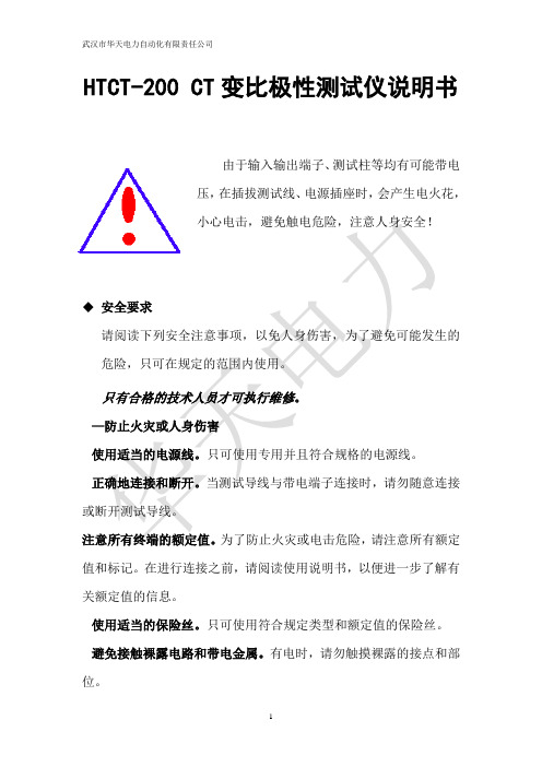
HTCT-200 CT变比极性测试仪说明书由于输入输出端子、测试柱等均有可能带电压,在插拔测试线、电源插座时,会产生电火花,小心电击,避免触电危险,注意人身安全!安全要求请阅读下列安全注意事项,以免人身伤害,为了避免可能发生的危险,只可在规定的范围内使用。
只有合格的技术人员才可执行维修。
—防止火灾或人身伤害使用适当的电源线。
只可使用专用并且符合规格的电源线。
正确地连接和断开。
当测试导线与带电端子连接时,请勿随意连接或断开测试导线。
注意所有终端的额定值。
为了防止火灾或电击危险,请注意所有额定值和标记。
在进行连接之前,请阅读使用说明书,以便进一步了解有关额定值的信息。
使用适当的保险丝。
只可使用符合规定类型和额定值的保险丝。
避免接触裸露电路和带电金属。
有电时,请勿触摸裸露的接点和部位。
请勿在潮湿环境下操作。
请勿在易爆环境中操作。
-安全术语警告:警告字句指出可能造成人身伤亡的状况或做法。
目录一、面板说明 (6)二、使用方法 (6)三、技术指标 (7)四、设备配件 (8)HTCT-200 CT变比极性测试仪根据JJG313-94《测量用电流互感器》,要求互感器交接时和更换绕组后必须进行现场变比检查试验。
常规互感器变比的检查方法是电流法,从原理上讲是一种容易理解可行的检查方法,但是随着系统容量的增加,电流互感器的一次电流越来越大,最大可达数万安培;现场加电流至数百安培已有困难,数千安培或数万安培几乎不可能,况且体积庞大,重量重达几百公斤或几吨,现场使用更为困难,如采用小电流法,由于电流互感器磁感度、线性度、阻抗、漏抗的影响会使电流互感器误差骤增,失去了变比检查的意义。
体积小、重量轻、测量范围广、便于携带,适于现场使用的电流互感器变比测试仪越来越成为互感器测试工作的必备手段。
HTCT-200 CT变比极性测试仪就是我公司总结国内外互感器特性,运用目前最新研究理论及成果,结合现场使用的要求研制而成的,它有如下特点:1、首家采用电压测量法,体积小重量轻,便携式,满足现场工作轻便性要求。
XXHDS产品优势介绍yx

HPQ XP256 XP48 XP512 XP128 XP1024 XP10000 XP12000 XP 24000
SUN N/A SE9910 SE9960 SE9970 SE9980 SE9985 SE9990 SE9990V
学习改变命运,知 识创造未来
XXHDS产品优势介绍yx
各厂商磁盘产品
• HDS独有虚拟端口模式
– 每一个物理端口支持128个异构主机 平台连接
• 各主机拥有自己的存储空间,没有数 据覆盖危险
• 多个LUN 0 支持
– 更好的利用FC端口200MB/s的带宽
• 很多应用仅需要5-10MB/s的带宽
学习改变命运,知 识创造未来
•存储系统
•POR T
•AMS •Virtual Port
SE9985
SE9990
SE9990 V
• HP:高端存储全球OEM战略合作 • SUN:高端存储全球联合品牌合作 • 联想、Gateway、Acer:中、低端模
块化存储联合品牌
学习改变命运,知 识创造未来
•直销 •代理商
•OEMs
•直销
•分销
XXHDS产品优势介绍yx
•代理商
•OE M
HDS中国区业务
• 4 iSCSI ports—2 per controller (Fibre Channel models available 2008)
• Supports SATA II (500GB or 750GB) or SAS (147GB or 300GB) HDDs
• 6, 8, or 12 HDDs per model, up to 9TB of capacity
• • • •
Pundit PL-200PE 商品说明书

®操作说明APundit 触摸屏B 电池C Pundit 脉冲回波传感器*D Pundit 脉冲回波电缆*E Pundit 脉冲回波接触测试板*F 电源G USB 线H DVD 光盘(含软件)I文档*J背带K校准卷尺**“Pundit 脉冲回波传感器”套装中的部件(产品编码 327 40 130)AFJGBHI 物品清单DECK333333333333 3.23Pundit PL-200PE 概述1123456789102目录1. 安全和责任 (5)1.1 通用信息 (5)1.2 责任 (5)1.3 安全说明 (5)1.4 正确使用 (5)2. 技术规格 (6)3. 使用 (7)3.1 入门指南 (7)3.2 主菜单 (8)3.3 设置 (8)3.4 测量屏幕 (10)3.5 测量模式 (11)3.6 用 Pundit PL-200PE 测量 (15)4. 资源管理器 (16)4.1 B-Scan 分析 (16)5. 订购信息 (17)5.1 单位 (17)5.2 传感器 (17)5.3 配件 .............................................176. 保养和支持 .. (18)6.1 保养 (18)6.2 支持理念 (18)6.3 保修信息 (18)6.4 废物处置 (18)7. PL-Link 软件 (18)7.1 启动 PL-Link (18)7.2 查看数据 (19)7.3 调整设置 (20)7.4 B-Scan 分析 (20)7.5 导出数据 (21)7.6 更多功能 (22)1. 安全和责任1.1 通用信息本手册包含了 Pundit PL-200PE 的安全、使用和保养等方面的重要信息。
请在首次使用仪器前仔细阅读本手册。
请安全保管本手册以备将来参考。
1.2 责任我们的“销售和交付一般条款”适用于所有情形。
由于下列某种或多种原因造成的人身伤害或财产损失,我们不予担保,也不承担任何责任:• 未按照本手册所述的使用方法使用该仪器。
HDSP-B04G中文资料

DescriptionThe 18:88 and 88:88 0.56" Four Digit Seven Segment Displays have surface painted in neutral gray and black for enhanced on/off contrast. All devices are available in either common anode or common cathode configuration with tinted green segments or untinted segments.Features•Excellent appearance•Evenly illuminated segments •Gray face for optimum on/off contrast •Choice of colors: Green•Choice of character size: 0.56 inchHDSP-B0xG18:88 and 88:88 0.56" Four Digit GaP Green Seven Segment DisplayData SheetFRONT SIDE2 – ∅1.70RIGHT SIDEA AA D DDC F EF E F EB C B C B C G G GDP3DP2DIGIT 2DIGIT 3DIGIT 4DIGIT 1A F EB G D NOTE:ALL DIMENSIONS ARE IN MILLIMETERS (INCHES).UNLESS OTHERWISE STATED, TOLERANCES ARE ± 0.25 mm.Pin Configuration Function Pin HDSP-B01G/B03G/B05G/B07G/B09G HDSP-B02G/B04G/B06G/B08G/B10G 1Anode E Cathode E 2Anode D Cathode D 3Anode DP Cathode DP 4Anode C Cathode C 5Anode GCathode G6Digit 4 Common Cathode Digit 4 Common Anode 7Anode BCathode B8Digit 3 Common Cathode Digit 3 Common Anode 9Digit 2 Common Cathode Digit 2 Common Anode 10Anode F Cathode F 11Anode ACathode A12Digit 1 Common CathodeDigit 1 Common AnodeFRONT SIDE2 – ∅1.70RIGHT SIDEA A A DDDB CF EF E F EB C B C B C G G GDP3DP2DIGIT 2DIGIT 3DIGIT 4DIGIT 1NOTE:ALL DIMENSIONS ARE IN MILLIMETERS (INCHES).UNLESS OTHERWISE STATED, TOLERANCES ARE ± 0.25 mm.HDSP-B01G and HDSP-B05G (Common Cathode)HDSP-B02G and HDSP-B06G (Common Anode)DIGIT 1DIGIT 2DIGIT 3DIGIT 4A 11B 7C 4D 2E 1F 10G 5DP 3DIGIT 1DIGIT 2DIGIT 3DIGIT 4A 11B 7C 4D 2E 1F 10G 5DP 3HDSP-B03G, HDSP-B07G, and HDSP-B09G (Common Cathode)HDSP-B04G, HDSP-B08G, and HDSP-B10G (Common Anode)DIGIT 1DIGIT 2DIGIT 3DIGIT 4A 11B 7C 4D 2E 1F 10G 5DP3DIGIT 1DIGIT 2DIGIT 3DIGIT 4A 11B 7C 4D 2E 1F 10G 5DP 3DevicesHDSP-DescriptionB01G88:88 0.56" Green 4 Digit, Tinted Green, Common Cathode, Display 18:88, Gray Color Surface B02G88:88 0.56" Green 4 Digit, Tinted Green, Common Anode, Display 18:88, Gray Color Surface B03G88:88 0.56" Green 4 Digit, Tinted Green, Common Cathode, Display 88:88, Gray Color Surface B04G88:88 0.56" Green 4 Digit, Tinted Green, Common Anode, Display 88:88, Gray Color Surface B05G88:88 0.56" Green 4 Digit, Untinted, Common Cathode, Display 18:88, Gray Color SurfaceB06G88:88 0.56" Green 4 Digit, Untinted, Common Anode, Display 18:88, Gray Color SurfaceB07G88:88 0.56" Green 4 Digit, Untinted, Common Cathode, Display 88:88, Gray Color SurfaceB08G88:88 0.56" Green 4 Digit, Untinted, Common Anode, Display 88:88, Gray Color SurfaceB09G88:88 0.56" Green 4 Digit, Untinted, Common Cathode, Display 88:88, Black Color SurfaceB10G88:88 0.56" Green 4 Digit, Untinted, Common Anode, Display 88:88, Black Color SurfacePart Numbering System5082 -X X X X-X X X X XHDSP-X X X X-X X X X XMechanical Options[1]00: No Mechanical OptionColor Bin Options[1,2]0: No Color Bin LimitationMaximum Intensity Bin[1,2]0: No Maximum Intensity Bin LimitationMinimum Intensity Bin[1,2]0: No Minimum Intensity Bin LimitationDevice Configuration/Color[1]G: GreenDevice Specific Configuration[1]Refer to Respective DatasheetPackage[1]Refer to Respective DatasheetNotes:1. For codes not listed in the figure above, please refer to the respective datasheet or contactyour nearest Avago representative for details.2. Bin options refer to shippable bins for a part number. Color and Intensity Bins are typicallyrestricted to 1 bin per tube (exceptions may apply). Please refer to respective datasheet forspecific bin limit information.Electrical/Optical Characteristics at T A = 25˚C Device Series HDSP-ParameterSymbol Min.Typ.Max.Units Test Conditions Luminous Intensity/SegmentI V20003200µcd I F = 10 mA(Digit Average)32004500All DevicesForward Voltage/Segment or DP V F 1.802.20 2.60V I F = 20 mA Peak Wavelength λPEAK 568nm I F = 20 mA Dominant Wavelength λd 573nmI F = 20 mA Luminous Intensity I V-M 2:1I F = 10 mA Matching Ratio Reverse CurrentI R100µAV R = 5 VNotes:1.Typical specification for reference only. Do not exceed absolute maximum ratings.2.The dominant wavelength, λd , is derived from the CIE chromaticity diagram and is that single wavelength which defines the color of the device.Absolute Maximum RatingsDescriptionGreen Units Average Power per Segment or DP65mW Peak Forward Current per Segment or DP 100mA DC Forward Current per Segment or DP 25mA Operating Temperature Range–40 to +105˚C Storage Temperature Range–40 to +105˚C Reverse Voltage per Segment or DP5V Wavesoldering Temperature for 3 seconds 2 mm below body250˚CNote:1.Derate above 40˚C at 0.33 mA/˚C for green.B01G, B02G, B03G, B04G B05G, B06G, B07G, B08G,B09G, B10G Intensity Bin Limits (µcd at 10 mA)Device Series HDSP-B01G, B02G, B03G, B04G B05G, B06G, B07G, B08G, B09G, B10GBin Name Min.[1]Max.[1]Min.[1]Max.[1]K 20003200NA NA L 3200505032005050MNA NA50508000Note:1.Tolerance for each bin limit is ±10%.Color Categories (Tolerance ± 1 nm)Rank Symbol Hue Range Unit 22573.5–576.5nm 33570.5–573.5nmContrast EnhancementFor information on contrast enhancement, please see Application Note 1015.Soldering/CleaningCleaning agents from the ketone family (acetone, methyl ethyl ketone, etc.) and from thechlorinated hydrocarbon family (methylene chloride,trichloroethylene, carbon tetrachloride, etc.) are notrecommended for cleaning LED parts. All these various solvents attack or dissolve theencapsulating epoxies used to form the package of plastic LED parts.Figure 1. Maximum allowable DC current vs.ambient temperature.Figure 2. Forward current vs. forward voltage.Figure 3. Relative luminous intensity vs. DC forward current.Figure 4. Relative efficiency (luminous intensity per unit current) vs. peak current.I D C – M A X I M U M D C C U R R E N T P E R S E G M E N T – m AT A – AMBIENT TEMPERATURE – °CI F – F O R W A R D C U R R E N T P E R S E G M E N T– m AV F – FORWARD VOLTAGE – VR E L A T I V E L U M I N O U S I N T E N S I T Y (N O R M A L I Z E D T O 1 A T 10 m AF O RG R E E N )I F – DC FORWARD CURRENT – mA8642R E L A T I V E E F F I C I E N C Y (N O R M A L I Z E D T O 1 A T 10 m A )1.4005101520253035404550PEAK FORWARD CURRENTPER SEGMENT – mA0.20.40.60.81.01.2For product information and a complete list of distributors, please go to our website: Avago, Avago Technologies, and the A logo are trademarks of Avago Technologies Limited in the United States and other countries.Data subject to change. Copyright © 2006 Avago Technologies Limited. All rights reserved. Obsoletes 5988-7859EN AV01-0698EN December 11, 2006。
HDS存储产品及方案简介

搜索、发现和集成独立的应用程序
内容云
基础架构云
基于基础架构、内容和信息的单一虚拟化平台
HDS解决方案一览
文件和内容服务 综合数据保护解决 助力企业成功 方案HDID CMM 融合基础架构UCP
存储管理解决方案 存储虚拟化SVOS
HDS公司一览
扩大产品组合并转变业务模式
近期收购
–
–
– –
BlueArc – 非结构化数据和大数据
ParaScale – 大数据横向扩展 Shoden Data Systems – 撒哈拉以南非洲地区
HDS三步云战略
分析 解锁企业暗数据
HDS愿景及战略
信息云
按需提供内容 归档服务
• 12Gb/s SAS • 1 port / CTL, Embedded
• 64GB: 2-CFM, 2-Bat, 4-DIMM • 32GB
Cache Subsystem File Options
• Always HNAS4000 gateways
VSP Gx00 DBS & DBL 磁盘柜信息
Front HDD
LFF (3.5”) x 60
Rear
PS ENC Rear Front
支持的磁盘类型
新增1.8TB SAS/1.9T SSD/10T NLSAS/14T FMD
支持跨扩展柜创建RAID
G200中端存储具备业界最高端的存储特性
全部内置存储虚 拟化 不停机数据迁移
支持重删和压缩功能 Hitachi企业级闪存 FMD支块1.2TB SAS盘
‒ IPSAN存储,适合普通OA应用或规模较小的客户 ‒ IOPS约3000,可用空间约20TB,支持10台以内的服务器连接
缸型电动缸DGE系列产品说明书

规格
8 12 18
L3 L4 L5 L6 L7 L11 L12 L13 L14 L15 L16 T1 T2 T3 T6 T7
± 0.1
+4 ±0.1 ±0.1
30 21 15.5 52 15
4 27.5 27.5 5
9.7 3.2
7
1.1 3.4 0.7 18.8
33 24 17 64 15
4 36.5 29
訂貨代號
DGE —
—
— ZR
—
—
型號 DGE
直線電動缸
規格
8 12, 18 25 40 63
行程 [mm]
1 ... 650 1 ... 1000 1 ... 3000 1 ... 4000 1 ... 4500
氣壓缸功能
ZR
齒輪皮帶電動缸
左側驅動軸
LK
左側無驅動軸
1
LV
驅動軸在左側,前面
2.2
LH
-H-
訂貨實例: DGE-63-500-ZR-LV-RK-KF-GK
-H- 注意
近接感測器的插入點,位於齒 輪皮帶電動缸DGE-ZR的右側。
O上 U下 R右 L左 V前 H後
— KF — GK
2-12
Key products, GCC-TW – Subject to change – 第一版
DGE-ZR-KF,
57
52.8 19.6 22.5
7
21.6
40
M5
M6
48
64
17
86
78
71.8 26.5
32
11.5
31
62
M8
M8
78
HDSP中文资料

Features• Low Power Consumption • Industry Standard Size• Industry Standard Pinout • Choice of Character Size7.6 mm (0.30 in), 10 mm (0.40 in), 10.9 mm (0.43 in), 14.2 mm (0.56 in), 20 mm (0.80 in)• Choice of ColorsAlGaAs Red, High Efficiency Red (HER), Yellow, Green• Excellent Appearance Evenly Lighted Segments±50° Viewing Angle• Design FlexibilityCommon Anode or Common CathodeSingle and Dual DigitLeft and Right Hand Decimal Points±1. Overflow Character• Categorized for Luminous IntensityYellow and Green Categorized for ColorUse of Like Categories Yields a Uniform Display• Excellent for Long Digit String Multiplexing DescriptionThese low current seven segment displays are designed for applica-tions requiring low power consumption. They are tested and selected for their excellent low current characteristics to ensure that the segments are matched at low currents. Drive currents as low as 1 mA per segment are available.Pin for pin equivalent displays are also available in a standard current or high light ambient design. The standard current displays are available in all colors and are ideal for most applica-tions. The high light ambient displays are ideal for sunlight ambients or long string lengths. For additional information see the 7.6 mm Micro Bright Seven Segment Displays, 10 mm Seven Segment Displays, 7.6 mm/10.9 mm Seven Segment Displays, 14.2 mm Seven Segment Displays, 20 mm Seven Segment Displays, or High Light Ambient Seven Segment Displays data sheets.Low Current Seven SegmentDisplays Technical Data HDSP-335x SeriesHDSP-555x SeriesHDSP-751x SeriesHDSP-A10x Series HDSP-A80x Series HDSP-A90x Series HDSP-E10x Series HDSP-F10x Series HDSP-G10x Series HDSP-H10x Series HDSP-K12x, K70x Series HDSP-N10x SeriesHDSP-N40x SeriesDevicesAlGaAs HER Yellow Green Package HDSP-HDSP-HDSP-HDSP-Description Drawing A1017511A801A9017.6 mm Common Anode Right Hand Decimal A A1037513A803A9037.6 mm Common Cathode Right Hand Decimal B A1077517A807A9077.6 mm Common Anode ±1. Overflow C A1087518A808A9087.6 mm Common Cathode ±1. Overflow D F10110 mm Common Anode Right Hand Decimal E F10310 mm Common Cathode Right Hand Decimal F F10710 mm Common Anode ±1. Overflow G F10810 mm Common Cathode ±1. Overflow H G10110 mm Two Digit Common Anode Right Hand Decimal X G10310 mm Two Digit Common Cathode Right Hand Decimal Y E100335010.9 mm Common Anode Left Hand Decimal I E101335110.9 mm Common Anode Right Hand Decimal J E103335310.9 mm Common Cathode Right Hand Decimal K E106335610.9 mm Universal ±1. Overflow[1]L H101555114.2 mm Common Anode Right Hand Decimal M H103555314.2 mm Common Cathode Right Hand Decimal N H107555714.2 mm Common Anode ±1. Overflow O H108555814.2 mm Common Cathode ±1. Overflow P K121K70114.2 mm Two Digit Common Anode Right Hand Decimal R K123K70314.2 mm Two Digit Common Cathode Right Hand Decimal S N10020 mm Common Anode Left Hand Decimal Q N101N40120 mm Common Anode Right Hand Decimal T N103N40320 mm Common Cathode Right Hand Decimal U N10520 mm Common Cathode Left Hand Decimal V N106N40620 mm Universal ±1. Overflow[1]W Note:1. Universal pinout brings the anode and cathode of each segment’s LED out to separate pins. See internal diagrams L or W.Part Numbering System5082-x xx x-x x x xxHDSP-x xx x-x x x xxMechanical Options[1]00: No mechanical optionColor Bin Options[1,2]0: No color bin limitationMaximum Intensity Bin[1,2]0: No maximum intensity bin limitationMinimum Intensity Bin[1,2]0: No minimum intensity bin limitationDevice Configuration/Color[1]G: GreenDevice Specific Configuration[1]Refer to respective datasheetPackage[1]Refer to Respective datasheetNotes:1. For codes not listed in the figure above, please refer to the respective datasheet or contact your nearest Agilent representative fordetails.2. Bin options refer to shippable bins for a part-number. Color and Intensity Bins are typically restricted to 1 bin per tube (excep-tions may apply). Please refer to respective datasheet for specific bin limit information.Package DimensionsPackage Dimensions (cont.)Package Dimensions (cont.)*The Side View of package indicates Country of Origin.Package Dimensions (cont.)Package Dimensions (cont.)Package Dimensions (cont.)Internal Circuit DiagramInternal Circuit Diagram (cont.)Absolute Maximum RatingsAlGaAs Red - HDSP-HERA10X/E10X/H10X HDSP-751X/Yellow GreenK12X/N10X/N40X335X/555X/HDSP-A80X HDSP-A90X Description F10X, G10X Series K70X Series Series Series Units Average Power per Segment or DP375264mW Peak Forward Current per 45mA Segment or DPDC Forward Current per15[1]15[2]mA Segment or DPOperating Temperature Range-20 to +100-40 to +100°C Storage Temperature Range -55 to +100°C Reverse Voltage per Segment 3.0V or DPWave Soldering Temperature for 3Seconds (1.60 mm [0.063 in.] below 250°C seating body)Notes:1. Derate above 91°C at 0.53 mA/°C.2. Derate HER/Yellow above 80°C at 0.38 mA/°C and Green above 71°C at 0.31 mA/°C.Electrical/Optical Characteristics at T A = 25°CAlGaAs RedDeviceSeriesHDSP-Parameter Symbol Min.Typ.Max.Units Test Conditions315600I F = 1 mA A10x3600I F = 5 mA330650I F = 1 mAF10x, G10x3900I F = 5 mA390650I F = 1 mA E10x Luminous Intensity/Segment[1,2]I Vµcd(Digit Average)3900I F = 5 mA400700I F = 1 mAH10x, K12x4200I F = 5 mA270590I F = 1 mAN10x, N40x3500I F = 5 mA1.6I F = 1 mAForward Voltage/Segment or DP V F 1.7V I F = 5 mA1.82.2I F = 20 mA PkAll Devices Peak WavelengthλPEAK645nmDominant Wavelength[3]λd637nmReverse Voltage/Segment or DP[4]V R 3.015V I R = 100 µATemperature Coefficient of∆V F/°C-2 mV mV/°CV F/Segment or DPA10x255F10x, G10x320E10x340Thermal Resistance LED RθJ-PIN°C/W/SegH10x, K12x Junction-to-Pin400N10x, N40x430High Efficiency RedDeviceSeriesHDSP-Parameter Symbol Min.Typ.Max.Units Test Conditions160270I F = 2 mA 751x1050I F = 5 mA200300I F = 2 mA Luminous Intensity/Segment[1,2]I V mcd(Digit Average)1200I F = 5 mA335x, 555x,K70x270370I F = 2 mA1480I F = 5 mA1.6I F = 2 mAForward Voltage/Segment or DP V F 1.7V I F = 5 mA2.1 2.5I F = 20 mA Pk All Devices Peak WavelengthλPEAK635nmDominant Wavelength[3]λd626nmReverse Voltage/Segment or DP[4]V R 3.030V I R = 100 µATemperature Coefficient of∆V F/°C-2mV/°CV F/Segment or DP751x200335x Thermal Resistance LED RθJ-PIN280°C/WJunction-to-Pin555x, K70x345YellowDeviceSeriesHDSP-Parameter Symbol Min.Typ.Max.Units Test Conditions Luminous Intensity/Segment[1,2]250420I F = 4 mA(Digit Average)I V mcd1300I F = 10 mA1.7I F = 4 mAForward Voltage/Segment or DP V F 1.8V I F = 5 mA A80x2.1 2.5I F = 20 mA PkPeak WavelengthλPEAK583nmDominant Wavelength[3,5]λd581.5585592.5nmReverse Voltage/Segment or DP[4]V R 3.030V I R = 100 µATemperature Coefficient of∆V F/°C-2mV/°CV F/Segment or DPThermal Resistance LED RθJ-PIN200°C/WJunction-to-PinGreenDeviceSeriesHDSP-Parameter Symbol Min.Typ.Max.Units Test Conditions Luminous Intensity/Segment[1,2]250475I F = 4 mA(Digit Average)I V mcd1500I F = 10 mA1.9I F = 4 mAForward Voltage/Segment or DP V F 2.0V I F = 10 mA A90x2.1 2.5I F = 20 mA PkPeak WavelengthλPEAK566nmDominant Wavelength[3,5]λd571577nmReverse Voltage/Segment or DP[4]V R 3.030V I R = 100 µATemperature Coefficient of∆V F/°C-2mV/°CV F/Segment or DPThermal Resistance LED RθJ-PIN200°C/WJunction-to-PinNotes:1. Device case temperature is 25°C prior to the intensity measurement.2. The digits are categorized for luminous intensity. The intensity category is designated by a letter on the side of the package.3. The dominant wavelength, λd, is derived from the CIE chromaticity diagram and is the single wavelength which defines the color of thedevice.4. Typical specification for reference only. Do not exceed absolute maximum ratings.5. The yellow (HDSP-A800) and Green (HDSP-A900) displays are categorized for dominant wavelength. The category is designated by anumber adjacent to the luminous intensity category letter.AlGaAs RedIntensity Bin Limits (mcd)AlGaAs RedHDSP-A10xIV Bin Category Min.Max.E0.3150.520F0.4280.759G0.621 1.16H0.945 1.71I 1.40 2.56J 2.10 3.84K 3.14 5.75L 4.708.55HDSP-E10x/F10x/G10xIV Bin Category Min.Max.D0.3910.650E0.5320.923F0.755 1.39G 1.13 2.08H 1.70 3.14HDSP-H10x/K12xIV Bin Category Min.Max.C0.4150.690D0.5650.990E0.810 1.50F 1.20 2.20G 1.80 3.30H 2.73 5.00I 4.097.50HDSP-N10xIV Bin Category Min.Max.A0.2700.400B0.3250.500C0.4150.690D0.5650.990E0.810 1.50F 1.20 2.20G 1.80 3.30H 2.73 5.00I 4.097.50Intensity Bin Limits (mcd), continued HERHDSP-751xIV Bin Category Min.Max.B0.1600.240C0.2000.300D0.2500.385E0.3150.520F0.4280.759G0.621 1.16HDSP-751xIV Bin Category Min.Max.B0.2400.366C0.3000.477D0.3910.650E0.5320.923F0.755 1.39G 1.13 2.08H 1.70 3.14HDSP-555x/K70xIV Bin Category Min.Max.A0.2700.400B0.3250.500C0.4150.690D0.5650.990E0.810 1.50F 1.20 2.20G 1.80 3.30H 2.73 5.00I 4.097.50Intensity Bin Limits (mcd), continued YellowHDSP-A80xIV Bin Category Min.Max.D0.2500.385E0.3150.520F0.4250.760G0.625 1.14H0.940 1.70I 1.40 2.56J 2.10 3.84K 3.14 5.76L 4.718.64M7.0713.00N10.6019.40O15.9029.20P23.9043.80Q35.8065.60GreenHDSP-A90xIV Bin Category Min.Max.E0.3150.520F0.4250.760G0.625 1.14H0.940 1.70I 1.40 2.56J 2.10 3.84K 3.14 5.76L 4.718.64M7.0713.00N10.6019.40O15.9029.20P23.9043.80Q35.8065.60Electrical/OpticalFor more information on electrical/optical characteristics, please see Application Note 1005.Contrast Enhancement For information on contrast enhancement, please see Application Note 1015.Soldering/Cleaning Cleaning agents from the ketone family (acetone, methyl ethyl ketone, etc.) and from the chorinated hydrocarbon family (methylene chloride, trichloro-ethylene, carbon tetrachloride, etc.) are not recommended for cleaning LED parts. All of these various solvents attack or dissolve the encapsulating epoxies used to form the package of plastic LED parts.For information on soldering LEDs, please refer to Application Note 1027.Note:All categories are established for classification of products. Productsmay not be available in all categories. Please contact your localAgilent representatives for further clarification/information.Color Categories/semiconductorsFor product information and a complete list ofdistributors, please go to our web site.For technical assistance call:Americas/Canada: +1 (800) 235-0312 or(916) 788 6763Europe: +49 (0) 6441 92460China: 10800 650 0017Hong Kong: (+65) 6271 2451India, Australia, New Zealand: (+65) 6271 2394Japan: (+81 3) 3335-8152(Domestic/International), or0120-61-1280(Domestic Only)Korea: (+65) 6271 2194Malaysia, Singapore: (+65) 6271 2054Taiwan: (+65) 6271 2654Data subject to change.Copyright © 2005 Agilent Technologies, Inc.Obsoletes 5988-8412ENJanuary 19, 20055989-0080EN。
HDSP-F107-H0000中文资料

Features• Low Power Consumption • Industry Standard Size• Industry Standard Pinout • Choice of Character Size7.6 mm (0.30 in), 10 mm (0.40 in), 10.9 mm (0.43 in), 14.2 mm (0.56 in), 20 mm (0.80 in)• Choice of ColorsAlGaAs Red, High Efficiency Red (HER), Yellow, Green• Excellent Appearance Evenly Lighted Segments±50° Viewing Angle• Design FlexibilityCommon Anode or Common CathodeSingle and Dual DigitLeft and Right Hand Decimal Points±1. Overflow Character• Categorized for Luminous IntensityYellow and Green Categorized for ColorUse of Like Categories Yields a Uniform Display• Excellent for Long Digit String Multiplexing DescriptionThese low current seven segment displays are designed for applica-tions requiring low power consumption. They are tested and selected for their excellent low current characteristics to ensure that the segments are matched at low currents. Drive currents as low as 1 mA per segment are available.Pin for pin equivalent displays are also available in a standard current or high light ambient design. The standard current displays are available in all colors and are ideal for most applica-tions. The high light ambient displays are ideal for sunlight ambients or long string lengths. For additional information see the 7.6 mm Micro Bright Seven Segment Displays, 10 mm Seven Segment Displays, 7.6 mm/10.9 mm Seven Segment Displays, 14.2 mm Seven Segment Displays, 20 mm Seven Segment Displays, or High Light Ambient Seven Segment Displays data sheets.Low Current Seven SegmentDisplays Technical Data HDSP-335x SeriesHDSP-555x SeriesHDSP-751x SeriesHDSP-A10x Series HDSP-A80x Series HDSP-A90x Series HDSP-E10x Series HDSP-F10x Series HDSP-G10x Series HDSP-H10x Series HDSP-K12x, K70x Series HDSP-N10x SeriesHDSP-N40x SeriesDevicesAlGaAs HER Yellow Green Package HDSP-HDSP-HDSP-HDSP-Description Drawing A1017511A801A9017.6 mm Common Anode Right Hand Decimal A A1037513A803A9037.6 mm Common Cathode Right Hand Decimal B A1077517A807A9077.6 mm Common Anode ±1. Overflow C A1087518A808A9087.6 mm Common Cathode ±1. Overflow D F10110 mm Common Anode Right Hand Decimal E F10310 mm Common Cathode Right Hand Decimal F F10710 mm Common Anode ±1. Overflow G F10810 mm Common Cathode ±1. Overflow H G10110 mm Two Digit Common Anode Right Hand Decimal X G10310 mm Two Digit Common Cathode Right Hand Decimal Y E100335010.9 mm Common Anode Left Hand Decimal I E101335110.9 mm Common Anode Right Hand Decimal J E103335310.9 mm Common Cathode Right Hand Decimal K E106335610.9 mm Universal ±1. Overflow[1]L H101555114.2 mm Common Anode Right Hand Decimal M H103555314.2 mm Common Cathode Right Hand Decimal N H107555714.2 mm Common Anode ±1. Overflow O H108555814.2 mm Common Cathode ±1. Overflow P K121K70114.2 mm Two Digit Common Anode Right Hand Decimal R K123K70314.2 mm Two Digit Common Cathode Right Hand Decimal S N10020 mm Common Anode Left Hand Decimal Q N101N40120 mm Common Anode Right Hand Decimal T N103N40320 mm Common Cathode Right Hand Decimal U N10520 mm Common Cathode Left Hand Decimal V N106N40620 mm Universal ±1. Overflow[1]W Note:1. Universal pinout brings the anode and cathode of each segment’s LED out to separate pins. See internal diagrams L or W.Part Numbering System5082-x xx x-x x x xxHDSP-x xx x-x x x xxMechanical Options[1]00: No mechanical optionColor Bin Options[1,2]0: No color bin limitationMaximum Intensity Bin[1,2]0: No maximum intensity bin limitationMinimum Intensity Bin[1,2]0: No minimum intensity bin limitationDevice Configuration/Color[1]G: GreenDevice Specific Configuration[1]Refer to respective datasheetPackage[1]Refer to Respective datasheetNotes:1. For codes not listed in the figure above, please refer to the respective datasheet or contact your nearest Agilent representative fordetails.2. Bin options refer to shippable bins for a part-number. Color and Intensity Bins are typically restricted to 1 bin per tube (excep-tions may apply). Please refer to respective datasheet for specific bin limit information.Package DimensionsPackage Dimensions (cont.)Package Dimensions (cont.)*The Side View of package indicates Country of Origin.Package Dimensions (cont.)Package Dimensions (cont.)Package Dimensions (cont.)Internal Circuit DiagramInternal Circuit Diagram (cont.)Absolute Maximum RatingsAlGaAs Red - HDSP-HERA10X/E10X/H10X HDSP-751X/Yellow GreenK12X/N10X/N40X335X/555X/HDSP-A80X HDSP-A90X Description F10X, G10X Series K70X Series Series Series Units Average Power per Segment or DP375264mW Peak Forward Current per 45mA Segment or DPDC Forward Current per15[1]15[2]mA Segment or DPOperating Temperature Range-20 to +100-40 to +100°C Storage Temperature Range -55 to +100°C Reverse Voltage per Segment 3.0V or DPWave Soldering Temperature for 3Seconds (1.60 mm [0.063 in.] below 250°C seating body)Notes:1. Derate above 91°C at 0.53 mA/°C.2. Derate HER/Yellow above 80°C at 0.38 mA/°C and Green above 71°C at 0.31 mA/°C.Electrical/Optical Characteristics at T A = 25°CAlGaAs RedDeviceSeriesHDSP-Parameter Symbol Min.Typ.Max.Units Test Conditions315600I F = 1 mA A10x3600I F = 5 mA330650I F = 1 mAF10x, G10x3900I F = 5 mA390650I F = 1 mA E10x Luminous Intensity/Segment[1,2]I Vµcd(Digit Average)3900I F = 5 mA400700I F = 1 mAH10x, K12x4200I F = 5 mA270590I F = 1 mAN10x, N40x3500I F = 5 mA1.6I F = 1 mAForward Voltage/Segment or DP V F 1.7V I F = 5 mA1.82.2I F = 20 mA PkAll Devices Peak WavelengthλPEAK645nmDominant Wavelength[3]λd637nmReverse Voltage/Segment or DP[4]V R 3.015V I R = 100 µATemperature Coefficient of∆V F/°C-2 mV mV/°CV F/Segment or DPA10x255F10x, G10x320E10x340Thermal Resistance LED RθJ-PIN°C/W/SegH10x, K12x Junction-to-Pin400N10x, N40x430High Efficiency RedDeviceSeriesHDSP-Parameter Symbol Min.Typ.Max.Units Test Conditions160270I F = 2 mA 751x1050I F = 5 mA200300I F = 2 mA Luminous Intensity/Segment[1,2]I V mcd(Digit Average)1200I F = 5 mA335x, 555x,K70x270370I F = 2 mA1480I F = 5 mA1.6I F = 2 mAForward Voltage/Segment or DP V F 1.7V I F = 5 mA2.1 2.5I F = 20 mA Pk All Devices Peak WavelengthλPEAK635nmDominant Wavelength[3]λd626nmReverse Voltage/Segment or DP[4]V R 3.030V I R = 100 µATemperature Coefficient of∆V F/°C-2mV/°CV F/Segment or DP751x200335x Thermal Resistance LED RθJ-PIN280°C/WJunction-to-Pin555x, K70x345YellowDeviceSeriesHDSP-Parameter Symbol Min.Typ.Max.Units Test Conditions Luminous Intensity/Segment[1,2]250420I F = 4 mA(Digit Average)I V mcd1300I F = 10 mA1.7I F = 4 mAForward Voltage/Segment or DP V F 1.8V I F = 5 mA A80x2.1 2.5I F = 20 mA PkPeak WavelengthλPEAK583nmDominant Wavelength[3,5]λd581.5585592.5nmReverse Voltage/Segment or DP[4]V R 3.030V I R = 100 µATemperature Coefficient of∆V F/°C-2mV/°CV F/Segment or DPThermal Resistance LED RθJ-PIN200°C/WJunction-to-PinGreenDeviceSeriesHDSP-Parameter Symbol Min.Typ.Max.Units Test Conditions Luminous Intensity/Segment[1,2]250475I F = 4 mA(Digit Average)I V mcd1500I F = 10 mA1.9I F = 4 mAForward Voltage/Segment or DP V F 2.0V I F = 10 mA A90x2.1 2.5I F = 20 mA PkPeak WavelengthλPEAK566nmDominant Wavelength[3,5]λd571577nmReverse Voltage/Segment or DP[4]V R 3.030V I R = 100 µATemperature Coefficient of∆V F/°C-2mV/°CV F/Segment or DPThermal Resistance LED RθJ-PIN200°C/WJunction-to-PinNotes:1. Device case temperature is 25°C prior to the intensity measurement.2. The digits are categorized for luminous intensity. The intensity category is designated by a letter on the side of the package.3. The dominant wavelength, λd, is derived from the CIE chromaticity diagram and is the single wavelength which defines the color of thedevice.4. Typical specification for reference only. Do not exceed absolute maximum ratings.5. The yellow (HDSP-A800) and Green (HDSP-A900) displays are categorized for dominant wavelength. The category is designated by anumber adjacent to the luminous intensity category letter.AlGaAs RedIntensity Bin Limits (mcd)AlGaAs RedHDSP-A10xIV Bin Category Min.Max.E0.3150.520F0.4280.759G0.621 1.16H0.945 1.71I 1.40 2.56J 2.10 3.84K 3.14 5.75L 4.708.55HDSP-E10x/F10x/G10xIV Bin Category Min.Max.D0.3910.650E0.5320.923F0.755 1.39G 1.13 2.08H 1.70 3.14HDSP-H10x/K12xIV Bin Category Min.Max.C0.4150.690D0.5650.990E0.810 1.50F 1.20 2.20G 1.80 3.30H 2.73 5.00I 4.097.50HDSP-N10xIV Bin Category Min.Max.A0.2700.400B0.3250.500C0.4150.690D0.5650.990E0.810 1.50F 1.20 2.20G 1.80 3.30H 2.73 5.00I 4.097.50Intensity Bin Limits (mcd), continued HERHDSP-751xIV Bin Category Min.Max.B0.1600.240C0.2000.300D0.2500.385E0.3150.520F0.4280.759G0.621 1.16HDSP-751xIV Bin Category Min.Max.B0.2400.366C0.3000.477D0.3910.650E0.5320.923F0.755 1.39G 1.13 2.08H 1.70 3.14HDSP-555x/K70xIV Bin Category Min.Max.A0.2700.400B0.3250.500C0.4150.690D0.5650.990E0.810 1.50F 1.20 2.20G 1.80 3.30H 2.73 5.00I 4.097.50Intensity Bin Limits (mcd), continued YellowHDSP-A80xIV Bin Category Min.Max.D0.2500.385E0.3150.520F0.4250.760G0.625 1.14H0.940 1.70I 1.40 2.56J 2.10 3.84K 3.14 5.76L 4.718.64M7.0713.00N10.6019.40O15.9029.20P23.9043.80Q35.8065.60GreenHDSP-A90xIV Bin Category Min.Max.E0.3150.520F0.4250.760G0.625 1.14H0.940 1.70I 1.40 2.56J 2.10 3.84K 3.14 5.76L 4.718.64M7.0713.00N10.6019.40O15.9029.20P23.9043.80Q35.8065.60Electrical/OpticalFor more information on electrical/optical characteristics, please see Application Note 1005.Contrast Enhancement For information on contrast enhancement, please see Application Note 1015.Soldering/Cleaning Cleaning agents from the ketone family (acetone, methyl ethyl ketone, etc.) and from the chorinated hydrocarbon family (methylene chloride, trichloro-ethylene, carbon tetrachloride, etc.) are not recommended for cleaning LED parts. All of these various solvents attack or dissolve the encapsulating epoxies used to form the package of plastic LED parts.For information on soldering LEDs, please refer to Application Note 1027.Note:All categories are established for classification of products. Productsmay not be available in all categories. Please contact your localAgilent representatives for further clarification/information.Color Categories/semiconductorsFor product information and a complete list ofdistributors, please go to our web site.For technical assistance call:Americas/Canada: +1 (800) 235-0312 or(916) 788 6763Europe: +49 (0) 6441 92460China: 10800 650 0017Hong Kong: (+65) 6271 2451India, Australia, New Zealand: (+65) 6271 2394Japan: (+81 3) 3335-8152(Domestic/International), or0120-61-1280(Domestic Only)Korea: (+65) 6271 2194Malaysia, Singapore: (+65) 6271 2054Taiwan: (+65) 6271 2654Data subject to change.Copyright © 2005 Agilent Technologies, Inc.Obsoletes 5988-8412ENJanuary 19, 20055989-0080EN。
5082-K121-GF000中文资料
Features• Low Power Consumption • Industry Standard Size• Industry Standard Pinout • Choice of Character Size7.6 mm (0.30 in), 10 mm (0.40 in), 10.9 mm (0.43 in), 14.2 mm (0.56 in), 20 mm (0.80 in)• Choice of ColorsAlGaAs Red, High Efficiency Red (HER), Yellow, Green• Excellent Appearance Evenly Lighted Segments±50° Viewing Angle• Design FlexibilityCommon Anode or Common CathodeSingle and Dual DigitLeft and Right Hand Decimal Points±1. Overflow Character• Categorized for Luminous IntensityYellow and Green Categorized for ColorUse of Like Categories Yields a Uniform Display• Excellent for Long Digit String Multiplexing DescriptionThese low current seven segment displays are designed for applica-tions requiring low power consumption. They are tested and selected for their excellent low current characteristics to ensure that the segments are matched at low currents. Drive currents as low as 1 mA per segment are available.Pin for pin equivalent displays are also available in a standard current or high light ambient design. The standard current displays are available in all colors and are ideal for most applica-tions. The high light ambient displays are ideal for sunlight ambients or long string lengths. For additional information see the 7.6 mm Micro Bright Seven Segment Displays, 10 mm Seven Segment Displays, 7.6 mm/10.9 mm Seven Segment Displays, 14.2 mm Seven Segment Displays, 20 mm Seven Segment Displays, or High Light Ambient Seven Segment Displays data sheets.Low Current Seven SegmentDisplays Technical Data HDSP-335x SeriesHDSP-555x SeriesHDSP-751x SeriesHDSP-A10x Series HDSP-A80x Series HDSP-A90x Series HDSP-E10x Series HDSP-F10x Series HDSP-G10x Series HDSP-H10x Series HDSP-K12x, K70x Series HDSP-N10x SeriesHDSP-N40x SeriesDevicesAlGaAs HER Yellow Green Package HDSP-HDSP-HDSP-HDSP-Description Drawing A1017511A801A9017.6 mm Common Anode Right Hand Decimal A A1037513A803A9037.6 mm Common Cathode Right Hand Decimal B A1077517A807A9077.6 mm Common Anode ±1. Overflow C A1087518A808A9087.6 mm Common Cathode ±1. Overflow D F10110 mm Common Anode Right Hand Decimal E F10310 mm Common Cathode Right Hand Decimal F F10710 mm Common Anode ±1. Overflow G F10810 mm Common Cathode ±1. Overflow H G10110 mm Two Digit Common Anode Right Hand Decimal X G10310 mm Two Digit Common Cathode Right Hand Decimal Y E100335010.9 mm Common Anode Left Hand Decimal I E101335110.9 mm Common Anode Right Hand Decimal J E103335310.9 mm Common Cathode Right Hand Decimal K E106335610.9 mm Universal ±1. Overflow[1]L H101555114.2 mm Common Anode Right Hand Decimal M H103555314.2 mm Common Cathode Right Hand Decimal N H107555714.2 mm Common Anode ±1. Overflow O H108555814.2 mm Common Cathode ±1. Overflow P K121K70114.2 mm Two Digit Common Anode Right Hand Decimal R K123K70314.2 mm Two Digit Common Cathode Right Hand Decimal S N10020 mm Common Anode Left Hand Decimal Q N101N40120 mm Common Anode Right Hand Decimal T N103N40320 mm Common Cathode Right Hand Decimal U N10520 mm Common Cathode Left Hand Decimal V N106N40620 mm Universal ±1. Overflow[1]W Note:1. Universal pinout brings the anode and cathode of each segment’s LED out to separate pins. See internal diagrams L or W.Part Numbering System5082-x xx x-x x x xxHDSP-x xx x-x x x xxMechanical Options[1]00: No mechanical optionColor Bin Options[1,2]0: No color bin limitationMaximum Intensity Bin[1,2]0: No maximum intensity bin limitationMinimum Intensity Bin[1,2]0: No minimum intensity bin limitationDevice Configuration/Color[1]G: GreenDevice Specific Configuration[1]Refer to respective datasheetPackage[1]Refer to Respective datasheetNotes:1. For codes not listed in the figure above, please refer to the respective datasheet or contact your nearest Agilent representative fordetails.2. Bin options refer to shippable bins for a part-number. Color and Intensity Bins are typically restricted to 1 bin per tube (excep-tions may apply). Please refer to respective datasheet for specific bin limit information.Package DimensionsPackage Dimensions (cont.)Package Dimensions (cont.)*The Side View of package indicates Country of Origin.Package Dimensions (cont.)Package Dimensions (cont.)Package Dimensions (cont.)Internal Circuit DiagramInternal Circuit Diagram (cont.)Absolute Maximum RatingsAlGaAs Red - HDSP-HERA10X/E10X/H10X HDSP-751X/Yellow GreenK12X/N10X/N40X335X/555X/HDSP-A80X HDSP-A90X Description F10X, G10X Series K70X Series Series Series Units Average Power per Segment or DP375264mW Peak Forward Current per 45mA Segment or DPDC Forward Current per15[1]15[2]mA Segment or DPOperating Temperature Range-20 to +100-40 to +100°C Storage Temperature Range -55 to +100°C Reverse Voltage per Segment 3.0V or DPWave Soldering Temperature for 3Seconds (1.60 mm [0.063 in.] below 250°C seating body)Notes:1. Derate above 91°C at 0.53 mA/°C.2. Derate HER/Yellow above 80°C at 0.38 mA/°C and Green above 71°C at 0.31 mA/°C.Electrical/Optical Characteristics at T A = 25°CAlGaAs RedDeviceSeriesHDSP-Parameter Symbol Min.Typ.Max.Units Test Conditions315600I F = 1 mA A10x3600I F = 5 mA330650I F = 1 mAF10x, G10x3900I F = 5 mA390650I F = 1 mA E10x Luminous Intensity/Segment[1,2]I Vµcd(Digit Average)3900I F = 5 mA400700I F = 1 mAH10x, K12x4200I F = 5 mA270590I F = 1 mAN10x, N40x3500I F = 5 mA1.6I F = 1 mAForward Voltage/Segment or DP V F 1.7V I F = 5 mA1.82.2I F = 20 mA PkAll Devices Peak WavelengthλPEAK645nmDominant Wavelength[3]λd637nmReverse Voltage/Segment or DP[4]V R 3.015V I R = 100 µATemperature Coefficient of∆V F/°C-2 mV mV/°CV F/Segment or DPA10x255F10x, G10x320E10x340Thermal Resistance LED RθJ-PIN°C/W/SegH10x, K12x Junction-to-Pin400N10x, N40x430High Efficiency RedDeviceSeriesHDSP-Parameter Symbol Min.Typ.Max.Units Test Conditions160270I F = 2 mA 751x1050I F = 5 mA200300I F = 2 mA Luminous Intensity/Segment[1,2]I V mcd(Digit Average)1200I F = 5 mA335x, 555x,K70x270370I F = 2 mA1480I F = 5 mA1.6I F = 2 mAForward Voltage/Segment or DP V F 1.7V I F = 5 mA2.1 2.5I F = 20 mA Pk All Devices Peak WavelengthλPEAK635nmDominant Wavelength[3]λd626nmReverse Voltage/Segment or DP[4]V R 3.030V I R = 100 µATemperature Coefficient of∆V F/°C-2mV/°CV F/Segment or DP751x200335x Thermal Resistance LED RθJ-PIN280°C/WJunction-to-Pin555x, K70x345YellowDeviceSeriesHDSP-Parameter Symbol Min.Typ.Max.Units Test Conditions Luminous Intensity/Segment[1,2]250420I F = 4 mA(Digit Average)I V mcd1300I F = 10 mA1.7I F = 4 mAForward Voltage/Segment or DP V F 1.8V I F = 5 mA A80x2.1 2.5I F = 20 mA PkPeak WavelengthλPEAK583nmDominant Wavelength[3,5]λd581.5585592.5nmReverse Voltage/Segment or DP[4]V R 3.030V I R = 100 µATemperature Coefficient of∆V F/°C-2mV/°CV F/Segment or DPThermal Resistance LED RθJ-PIN200°C/WJunction-to-PinGreenDeviceSeriesHDSP-Parameter Symbol Min.Typ.Max.Units Test Conditions Luminous Intensity/Segment[1,2]250475I F = 4 mA(Digit Average)I V mcd1500I F = 10 mA1.9I F = 4 mAForward Voltage/Segment or DP V F 2.0V I F = 10 mA A90x2.1 2.5I F = 20 mA PkPeak WavelengthλPEAK566nmDominant Wavelength[3,5]λd571577nmReverse Voltage/Segment or DP[4]V R 3.030V I R = 100 µATemperature Coefficient of∆V F/°C-2mV/°CV F/Segment or DPThermal Resistance LED RθJ-PIN200°C/WJunction-to-PinNotes:1. Device case temperature is 25°C prior to the intensity measurement.2. The digits are categorized for luminous intensity. The intensity category is designated by a letter on the side of the package.3. The dominant wavelength, λd, is derived from the CIE chromaticity diagram and is the single wavelength which defines the color of thedevice.4. Typical specification for reference only. Do not exceed absolute maximum ratings.5. The yellow (HDSP-A800) and Green (HDSP-A900) displays are categorized for dominant wavelength. The category is designated by anumber adjacent to the luminous intensity category letter.Figure 1. Maximum AllowableAverage or DC Current vs. Ambient Temperature.Figure 2. Forward Current vs.Forward Voltage.AlGaAs RedFigure 4. Relative Efficiency (Luminous Intensity per UnitCurrent) vs. Peak Current.Figure 3. Relative Luminous Intensity vs. DC Forward Current.Figure 5. Maximum Allowable Average or DC Current vs. Ambient Temperature.Figure 6. Forward Current vs. Forward Voltage.HER, Yellow, GreenFigure 7. Relative Luminous Intensityvs. DC Forward Current.Figure 8. Relative Efficiency(Luminous Intensity per UnitCurrent) vs. Peak Current.Intensity Bin Limits (mcd)AlGaAs RedHDSP-A10xIV Bin Category Min.Max.E0.3150.520F0.4280.759G0.621 1.16H0.945 1.71I 1.40 2.56J 2.10 3.84K 3.14 5.75L 4.708.55HDSP-E10x/F10x/G10xIV Bin Category Min.Max.D0.3910.650E0.5320.923F0.755 1.39G 1.13 2.08H 1.70 3.14HDSP-H10x/K12xIV Bin Category Min.Max.C0.4150.690D0.5650.990E0.810 1.50F 1.20 2.20G 1.80 3.30H 2.73 5.00I 4.097.50HDSP-N10xIV Bin Category Min.Max.A0.2700.400B0.3250.500C0.4150.690D0.5650.990E0.810 1.50F 1.20 2.20G 1.80 3.30H 2.73 5.00I 4.097.50Intensity Bin Limits (mcd), continued HERHDSP-751xIV Bin Category Min.Max.B0.1600.240C0.2000.300D0.2500.385E0.3150.520F0.4280.759G0.621 1.16HDSP-751xIV Bin Category Min.Max.B0.2400.366C0.3000.477D0.3910.650E0.5320.923F0.755 1.39G 1.13 2.08H 1.70 3.14HDSP-555x/K70xIV Bin Category Min.Max.A0.2700.400B0.3250.500C0.4150.690D0.5650.990E0.810 1.50F 1.20 2.20G 1.80 3.30H 2.73 5.00I 4.097.50Intensity Bin Limits (mcd), continued YellowHDSP-A80xIV Bin Category Min.Max.D0.2500.385E0.3150.520F0.4250.760G0.625 1.14H0.940 1.70I 1.40 2.56J 2.10 3.84K 3.14 5.76L 4.718.64M7.0713.00N10.6019.40O15.9029.20P23.9043.80Q35.8065.60GreenHDSP-A90xIV Bin Category Min.Max.E0.3150.520F0.4250.760G0.625 1.14H0.940 1.70I 1.40 2.56J 2.10 3.84K 3.14 5.76L 4.718.64M7.0713.00N10.6019.40O15.9029.20P23.9043.80Q35.8065.60Electrical/OpticalFor more information on electrical/optical characteristics, please see Application Note 1005.Contrast Enhancement For information on contrast enhancement, please see Application Note 1015.Soldering/Cleaning Cleaning agents from the ketone family (acetone, methyl ethyl ketone, etc.) and from the chorinated hydrocarbon family (methylene chloride, trichloro-ethylene, carbon tetrachloride, etc.) are not recommended for cleaning LED parts. All of these various solvents attack or dissolve the encapsulating epoxies used to form the package of plastic LED parts.For information on soldering LEDs, please refer to Application Note 1027.Note:All categories are established for classification of products. Productsmay not be available in all categories. Please contact your localAgilent representatives for further clarification/information.Color Categories/semiconductorsFor product information and a complete list ofdistributors, please go to our web site.For technical assistance call:Americas/Canada: +1 (800) 235-0312 or(916) 788 6763Europe: +49 (0) 6441 92460China: 10800 650 0017Hong Kong: (+65) 6271 2451India, Australia, New Zealand: (+65) 6271 2394Japan: (+81 3) 3335-8152(Domestic/International), or0120-61-1280(Domestic Only)Korea: (+65) 6271 2194Malaysia, Singapore: (+65) 6271 2054Taiwan: (+65) 6271 2654Data subject to change.Copyright © 2005 Agilent Technologies, Inc.Obsoletes 5988-8412ENJanuary 19, 20055989-0080EN。
PerkinElmer Series 200 Autosampler 产品手册说明书
Series200 Autosamplernew standardin automated sample processingSeries 200 AutosamplerDesigned to Meet All of Your…200 can easily be interfaced with a Zymark Twister to feed multiple microtiter plates!For even more power in your laboratory, add a TotalChrom ®Chromatography Workstation providing full HPLC system control, method and sequence documentation, and much more.And for biomolecular applications,the autosampler is available in a fully biocompatible flow path.So, take a look at the Series 200Autosampler – it truly is the standard in Automated Sample Processing.Precision at its best – from microbore to semi-prep Inject as little as 0.1 µL or as much as 2.5mL. Switch easily between standard industry syringes: 50, 100,250, 1000, or 2500 µL – without tools – to achieve the best precision in microbore to semi-prep injections using fixed or variable-fill modes.Choose from a variety of valves: the industry-standard Rheodyne ®7725,the Biocompatible 9725 or the 8125Micro-valve – which are available with optional rotor-seal materials including PEEK, Vespel ®,andTefzel®. Depending on your analy-sis, you can expect better than 0.5%RSD for volumes down to 3 µing the 8125 Micro-valve, this new design is truly optimized for microbore and LC/MS applications due to its low dispersion character-istics and excellent precision at lower injection volumes.Sample Injection Requirementsinstrument to the autosampler for immediate analysis withoutIndividual vial andmethod programmingwith “Dialog Box”Using the Dialog Box,define the range for each input:•••••Priority vial programming forurgent samplesNew Design Engineered forHighest Precision/Lowest MaintenanceThis figure demonstrates the excellent precision and linearity over a wide injection range.The %RSD is shown at each injection volume (10 replicates).The Series 200 Autosampler is optimized for the lowest carryover as shown by the 20-µL blank run after the 20-µL sample injection.Maximum Automationand Versatility Stand-alone or PC-based for complete system control and automationThe Series 200 Autosampler can operate as a stand-alone unit providing sophisticated automation including chaining together multiple methods with different injection sequences. The Series 200Autosampler can also be fully controlled as part of a TotalChrom LC Plus™ System –utilizing the industry-standard, award-winning TotalChrom Workstation.In a TotalChrom LC Plus system,the Series 200 Autosampler is under full-system, single-keyboard control, withcomplete documentation ofall injection and sequences parameters as well as additional programming capability.Additional programming features include unattended method development and sophisticated solvent optimization using Turbo Method DevelopmentSoftware. TotalChrom also provides the unique time-saving Sequence Template,where you simply designate the number of samples to be injected and the frequency of calibration – TotalChrom will automatically build the sequence for you so there is no need to reenter information.TotalChrom LC Plus will automatically create a sequence table after you designate the number of samples and the calibration frequency using the unique time-saving sequence template.TotalChrom LC Plus System including the Series 200 AutosamplerA variety of optionalinterchangeablesample trays forutmost convenienceThe Series 200 Autosamplersupports several interchange-able sample trays including a25-vial capacity tray with7-mL vials which may beuseful when you’re doingsemi-prep repeat injections ofthe same sample. Or perhapsyou’d prefer a 225-vialcapacity tray with 250-µL vialsfor maximum throughput. Thetrays can hold mini-, micro-,and standard vials crimp-capped or screw-capped. Weeven have several 96-well and384-well microtiter trays ableto support shallow or deep-well plates.Optional PeltierCooling accessoryAdd an optional MicrotiterPlate or 100-sample PeltierSample T ray for unattendedanalysis of temperature-labilesamples such as proteins andpeptides. The sample tempera-ture range is from 4 to 50 °C –all selectable from the keyboard. Choose from a variety of different trays toaccommodate different size vials for all of yoursampling needs.Integrated dilution and derivatization routines –without adding addi-tional hardware or cost Due to the unique XYZ design, the Series 200 Autosampler includes dilution and derivati-zation as part of the standard shipping unit. Transfer contents of one vial to another for applications such as diluting a series of vials to specified concentrations before injection or adding an internal standard or marker. Serial dilution is made easy with automated transfer of a specified amount of liquid between any two vials –this also permits automated preparation of standard dilu-tions from a single standard.For those samples requiring specialized precolumn chemistries such as OPA orFMOC, you can mix up to fivederivatizing reagents in the sample vial itself – you can even control the reaction time and the exact time of injection. This overcomes problems with sample chemistries with short half-lives. And if the tempera-ture needs to be under control, use the optional Peltier tray.Link the serial dilution routine to the analysis. You simply set up the autosampler to automatically prepare the calibrants and then go on to inject your samples with bracketed calibration. After the initial setup, you can start the whole process at any time by pressing one key.PerkinElmer Life andAnalytical Sciences710 Bridgeport AvenueShelton, CT 06484-4794 USAPhone: (800) 762-4000 or(+1) 203-925-4602For a complete listing of our global offices, visit /lasoffices©2006 PerkinElmer, Inc. All rights reserved. PerkinElmer is a registered trademark of PerkinElmer, Inc. TotalChrom and TotalChrom LC Plus are trademarks of PerkinElmer Inc. Teflon, Tefzel and Vespel are registered trademarks of E.I. dupont deNeumours & Company. Rheodyne is a registered trademark of Rheodyne, Inc. Twister is a trademark of Zymark, Inc. All trademarks depicted are the property of their respective holders or owners. PerkinElmer reserves the right to change this document at any time and disclaims liability for editorial, pictorial or typographical errors.001855H KG060603Printed in USA。
MasterLogic-200 Series 产品选择指南说明书
R32C-NS5A-40P TG7-1H40S
Relay Board Relay Board, 40point (For DO Sink Type only) Terminal Board Terminal Board, 40point
C40HF-15PB-1 C40HF-30PB-1
Cable Assembly for Terminal Board, 40p-40p, 1.5m Connection Cable
CPU
Power
Base
Expansion Driver Redundant
Expansion Driver Sync Cable
Max. I/O:23,808Pts., Redundant CPU, FO Max. I/O:23,808Pts., Redundant CPU, TP Redundant Power 110V, 5.5A Redundant Power 220V, 5.5A Redundant Power 110V, 8.5A Redundant Power 220V, 8.5A Redundant Power DC24V, 7.5A Main Base 2 slot Main Base 6 slot Expansion Base 8 slot Expansion Base 12 slot Redundant Expansion Base 12 slot Expansion Driver, TP Expansion Driver, FO Expansion Driver, TP/FO Redundant Expansion Driver, TP Redundant Expansion Driver, FO Redundant Expansion Driver, TP/FO Multimode Fiber Optic Cable, LC connector, 2.0m
Furukawa OFS 200

For Use With:200 µm ST and SMA Factory5 Termination Kits200 µm HCS ® Factory5 Fiber-Optic Cable ST and SMA Factory5 Crimp & Cleave ConnectorsCrimp & Cleave Termination Instructionsfor 200 µm Factory5 Cable with ST and SMA ConnectorsPlease Read FirstPlease make sure to READ and understand t ermination in-structions completely. Improper a ssembly will cause poor termination results and cause damage to termination kit com-ponents.Make sure you WEAR eye protection during the c leaving process. The bare fiber is sharp and may s plinter; handle very carefully. Make sure fiber is d isposed of properly, in a hard-sided container.OFS WARRANTS this t ermination kit to be free of defects for a period of 90 days from the date of purchase. Each kit is q ualified at our factory prior to shipment. OFS will, at their discretion, repair or replace any tools found to be defec-tive due to workmanship within the stated warranty period. (Excludes damage to the fiber stripper, cleave tool, and/or d iamond blade due to m isuse.)OFS recommends that all replacements or repairs be made at our manufacturing facility, except where specifically out-lined. Please C ONTACT the sales representative in your re-gion or call the factory for technical support:Monday-Friday, 8:00 am-5:00 pm EST.888-438-9936 [Toll free in the US and Canada]860-678-0371[International]Important Safety and Warranty Information888 438 9936 (US & Canada) or 860 678 0371 | iContent Page Factory5 ST and SMA Termination Kit Contents (1)Related Products and Accessories......................2-3 Factory5 ST and SMA Connectors (4)Termination InstructionsStep 1: Install strain relief boot (5)Step 2: Strip cable outer jacket ......................6-7 Step 3: Strip sub-unit outer jacket ....................8-9 Step 4: Strip fiber buffer..........................10-11 Step 5: Install cable anchor .. (12)Step 6: Install crimp sleeve .......................13-14 Step 7: Install ferrule . (15)Step 8: Crimp ferrule ............................16-18 Step 9: Cleave fiber .............................19-21 Step 10: Position strain relief boot ..................22-23 Diamond Cleave Tool Diagram .........................19Content Page Maintenance & Trouble Shooting GuideImportance of Cleave Tool Cleaning and Maintenance (24)Cleave Tool Cleaning Kit (24)Diamond Blade Replacement Kit (24)Trouble Shooting Guide (25)Termination and Test Kits Available (26)Trademark Information.........................Back Cover Table of ContentsFinal AssemblyFiber StripperBrushProng ToolScissorsCrimp ToolCable StripperDiamond CleaveToolFactory5 ST and SMA Termination Kit Contents888 438 9936 (US & Canada) or 860 678 0371 | 12 ST and SMA Termination Kit Contents continuedCP01229-02...........200 µm Fiber Stripper (White Blade Insert)with Cleaning Brush and Prong ToolAP01225.........................................ScissorsK16248.....................Booklet: Importance of Cleave ToolCleaning and MaintenanceOther Items Required (not included in kit): Safety Glasses, Marker3888 438 9936 (US & Canada) or 860 678 0371 | Termination kit contentscontinues onto the next pagePart Numbers DescriptionBT01827...............................SMA Positioner Plate (use to convert an ST kit to an SMA kit)BT01900................................ST Positioner Plate (use to convert an SMA kit to an ST kit)P10188-03 ........................Insertion Loss Test Kit for 200 µm ST Connectors P10188-05 ........................Insertion Loss Test Kit for 200 µm SMA Connectors P10188-08 ........................Insertion Loss Test Kit for 200 µm ST, SMA, V-Pin, and F07 Connectors P16247 ...........................Cleave Tool Cleaning Kit (Includes cleaning fluid and safe cleaning swabs)AT03290 ....................Diamond Blade Replacement KitNOTE:Only one component part replacement isrequired to convert an ST Termination Kit to its same size equivalent SMA TerminationKit and vice versa.Factory5 ST and SMA ConnectorsDescription Part NumbersSMA Connectors ..................................P18241ST Connectors ....................................P18242ST ConnectorBoot AnchorCrimp SleeveFerruleCapSMA ConnectorTermination InstructionsInstall Strain Relief Boot• S lide STRAIN RELIEF BOOT onto cable and move up andout of the way for easystripping.888 438 9936 (US & Canada) or 860 678 0371 | 56 Termination InstructionsSTEP2Strip Cable Outer Jacket• M ark cable outer jacket 3/4 inchesfrom the end with a marker.• S elect the 3.2 hole on the Cable Jacket Strip Toolto strip Cable Outer Jacket31/4”888 438 9936 (US & Canada) or 860 678 0371 | 7• V erify proper strip length against the strip template shown below.• C arefully unravel the aramid braid with a pointed instrument.• W hen the yarns are unravelled,cut them as closely to the cable outer jacket as possible.Slide scissors or other pointed object in this direction, carefully unravelling as many yarns at a time as is manageable withoutc reating a knot.88 Termination Instructions• S trip jacket using the 1.6 hole using the CABLEJACKET STRIP TOOL, apply a quick-but-partialsqueezing action (fully compressing the handles willcause the tool to incorrectly snap onto the fiber, possiblybreaking it), release and removethe outer jacket.3/4”• V erify proper strip length against thestrip template shown on page 7.888 438 9936 (US & Canada) or 860 678 0371 | 9Termination Instructions10NOTE:Be careful not to touch the HCS fiber coating once the fiber has been stripped. The coating will retain finger oils which can transfer to and damage the gripper pads in the cleaver during Step 9 in the termination process.STEP4Strip Fiber Buffer B efore you start:B e careful while handling the FIBER STRIPPER. Handle as a p recision device and do not strike on hard surfaces or drop.B e sure to clean blades frequently using small bristle brush sup-plied.IMPORTANT: Pull straight when stripping the fiber buffer. The HCS fiber cladding can be damaged if fiber is not pulled straight.• S eparate buffered fiber from yellow aramid yarn by pulling yarn back along the cable.NOTE:If unable to insert buffered fiber throughguide tube, trim tip of the fiber using scis-sors.NOTE:If a short length of cable is being termi-nated, wrap the cable around your hand to prevent fiber and aramid yarn from pulling out of cable.888 438 9936 (US & Canada) or 860 678 0371 | 11• I nsert the buffered fiber through the guide tube of the fiber stripper until the sub unit outer jacket b ottoms out inside the tube.• H olding cable securely, squeeze handles to cut buffer and PULL STRAIGHT to remove buffer.• I nspect HCS cladding for damage from improper buffer stripping. (i.e. white dusty stripe)• V erify proper buffer strip length against the strip template shown on page 7.NOTE:If damage is visible cut off the damagedfiber and repeat the procedure from Step 2: Strip Cable Outer Jacket.A p p r o x ima t e ly 1/8”M a x im u m 1/4”Termination Instructions12Install Cable Anchor• P ull aramid yarn strands back over stripped fiber.• H olding aramid yarn and fiber at very top. Feed the fiber and the aramid yarn through the CABLE ANCHOR. Bottom out the anchor on the cable sub-unit outer jacket using a clockwise turning motion. (i.e. screw the anchor onto the cable outer jacket, if n ecessary)• P osition anchor in CRIMP TOOL,centering the rear end of the anchor in the crimp nest.• S queeze crimp tool handles together until it clicks, then releases.STEP5NOTE:Be careful not to touch the HCS fiber coat-ing once the fiber has been stripped. The coating will retain finger oils which can transfer to and damage the gripper pads in the cleaver during Step 9 in the terminationprocess.888 438 9936 (US & Canada) or 860 678 0371 | 136Install Crimp Sleeve• D ivide the aramid yarn into approximately two equal halves.• F old both halves of the aramid yarn back over the cable an-chor. Be sure the fiber is centered in the cable anchor.• S lide the CRIMP SLEEVE over the cable anchor and aramid yarn until it bottoms out on the cable anchor.Step 6 continues onto the next pageCrimp from Step 5: Note position of aramid yarns in relation to this crimp. Maintain this position here and in Step 7.Termination Instructions14Install Crimp Sleeve continued• P osition the crimp sleeve in the CRIMP TOOL such that:• Squeeze crimp tool handles together.~ T he back edge of the crimp sleeve is aligned with the edge of the crimp nest.~ T he aramid yarn halves are positioned over thejaws.Crimp from Step 5: Note that the orientation of ar-amid yarns is maintained in relation to the jaws ofthe crimp tool.7Install Ferrule• F eed fiber through hole in rear of FERRULE.• S lide the ferrule for either SMA or ST connector down thefiber and into the crimp sleeve. Rotate to the o rientationshown below. Push the ferrule firmly until it bottoms out inthe crimp sleeve.SMA shown in illustrationKeyST shown in illustration888 438 9936 (US & Canada) or 860 678 0371 | 1516 Termination InstructionsSTEP8Crimp FerruleB efore you start:Make sure the ferrule is fully seated in the crimp sleeve.C heck to make sure the crimp die set is stamped properly for theconnector type, ‘SMA’ on one side and ‘ST’ on the other.P roper positioning of the connector in the die set is critical for aproper crimp location. Failure to crimp in the prescribed locationwill result in poor connector retention strength.C rimp dies can be reversed at the factory for left-handed opera-tors.SMA Connector• P osition the back of the SMA COUPLING NUT against the side of the crimp die set stamped‘SMA’ as shown.• R otate the SMA connector so that its l ocation dimple is oriented in the crimpdie set as shown.• S queeze CRIMP TOOL handles togetheruntil the tool releases.Step 8 continuesonto the next page17888 438 9936 (US & Canada) or 860 678 0371 | Termination Instructions18Crimp Ferrule continuedST Connector• P osition the back of the ST COUPLING NUT against the side of the crimp die set stamped ‘ST’.• R otate the ST connector so that its keyis oriented in the crimp die set as shown.• S queeze CRIMP TOOL handles together untilthe tool releases.KeywayKeywayTension SpringGripper PadsDiamond Blade & Anvil HousingPositioner PlateTrigger9Cleave Fiber B efore you start:Make sure the appropriate cleave tool positioner plate is beingused: SMA or STM ake sure the appropriate colored tension spring is being used: 200 µm = GREENR efer to diagram of the Cleave Tool.C areful while handling the Cleave Tool. Handle as a p recision de-vice and do not strike on hard surfaces or drop.K eep the cleave tool clean and free from oils, including naturally oc-curing finger oils. Gripper pads, diamond blade and anvil should be cleaned after every 50 cleaves. Use the OFS Cleave Tool Cleaning Kit — Part #P16247 - available separately.D o not use alcohol to clean the diamond blade or the gripper pads. Al-cohol will chemically react with the gripper pads and ruin them.D o not insert metal tools near the diamond blade, as it is fragile andmay chip.888 438 9936 (US & Canada) or 860 678 0371 | Step 9 continues onto the next page19Termination Instructions20NOTE:It is critical to fully insert the connector into the positioner plate. Failure to do so, may cause poor cleave quality and/or damage to the diamond blade.NOTE:Do not hold onto the connector during thecleave process. Doing so may cause poor cleave quality.STEP9Cleave Fiber continued• H olding the CLEAVING TOOL in a horizontal position, grip the handle while leaving your index finger free to actuate trig-ger.• P lace the ferrule into the hole of the positioner plate until it is fully inserted.• R elease the connector in the tool.• U sing index finger, slowly and gently depress trigger to perform the cleaveprocess. The cleave process is complete when the fiber snaps away from theconnector. Do not release trigger!• B efore releasing the trigger, remove the connector from the cleave tool andgrasp the top of the scrap fiber while releasing the trigger. Gently remove thescrap fiber while keeping it away from the diamond blade.• D ispose of scrap fiber safely in a hard-sided container.• I nstall protective cap onto connector to protect cleaved fiber surface.21888 438 9936 (US & Canada) or 860 678 0371 | 22 Termination InstructionsSTEP10Position Strain Relief Boot• U sing scissors, trim exposed aramid yarn as close to crimpsleeve as possible.• S lide strain relief boot onto connector (up to rear of couplingnut) to complete termination.888 438 9936 (US & Canada) or 860 678 0371 | 23Maintenance & Trouble Shooting GuideImportance of Cleave Tool Cleaningand MaintenanceThe Cleave Tool supplied with OFS’s Termination Kits con-tains movable parts, wear items, and a diamond blade that require regular maintenance, care, or replacement after useful life in order to perform satisfactorily. Damage and parts re-placement expense can result if recommended procedures are not followed.~T he diamond blade must be cleaned; the gripper pads must be cleaned, kept oil-free, and replaced after wear.~ The cleave-tool trigger must be depressed slowly.Cleave Tool Cleaning KitFor cleaning your cleave tool, please order the OFS Cleave Tool Cleaning Kit (part #P16247) which includes recom-mended cleaning fluid, swabs, and c omplete instructions. Diamond Blade Replacement KitFor replacing the diamond blade/anvil assembly, please order the Diamond Blade Replacement Kit (Part #AT03290.)The kit includes a new diamond blade, anvil, replacement screws, and complete instructions for performing this simple proce-dure at your facility.24Trouble Shooting Guide888 438 9936 (US & Canada) or 860 678 0371 | 2526 Termination and Test Kits AvailableOFS offers a specialized Termination Kit—and a ssociatedInsertion Loss Test Kit—for each type of Crimp &Cleave connector we support. These kits are availablein various combinations of sizes and/or connector types.Customer Relations at our factory can help you select thecorrect kit for your purposes.This document is for informational purposes only and is not intended to modify or supplement any OFS warranties or specifications relating to any of its products and services.Copyright © 2014 OFS Fitel, LLC.All Rights Reserved.081455 Darling Drive, Avon, CT 06001To learn more, please call or visit our website. Phone: 186****0371Toll Free: 188****9936Web: P18225 Rev. E Trademark Information:Manufactured in the USA by OFS.HCS is a registered trademark in the USA of OFS Fitel, LLC.。
HDS系列存储产品技术资料

HDS系列存储产品技术资料HDS存储目录第1章 HDS系列产品手册资料 (4)1.1 HDS VSP G1000(高端存储-1及高端存储扩容-1/2)产品介绍 (4)14.1.1概述 (4)14.1.2 VSP G1000产品亮点 (4)14.1.3 VSP G1000产品技术优势 (5)14.1.4 VSP G1000软件包 (14)14.1.5 VSP G1000产品技术指标 (25)1.2 HDS HUS-VM(高端存储-2/3及高端存储扩容-3/4)产品介绍 (30)14.2.1概述 (30)14.2.2 HUS VM技术的技术优势 (33)14.2.3HUS VM软件包 (40)14.2.4 HUS VM产品技术指标 (43)1.3 HDS VSP G200(中端存储1/2/3)产品介绍 (46)14.3.1概述 (46)14.3.2VSP Gx00系列产品亮点 (47)14.3.3 VSP Gx00技术优势 (48)14.3.4 VSP Gx00软件包 (49)14.3.5 VSP Gx00产品技术指标 (49)1.4 存储虚拟化兼容列表(VSP G1000/G200/HUS-VM通用) (54)1.5 HDS HCP(归档存储网关)产品介绍 (58)14.5.1什么是归档及其影响 (58)14.5.2归档平台与SAN和NAS的区别 (60)14.5.3HCP 概述 (61)14.5.4HCP优势 (62)14.5.5HCP功能介绍 (63)1.6 HDS Brocade 6510(光纤交换机-1/2及光纤交换机扩容)产品介绍 (69)14.6.1 亮点 (69)14.6.2 概述 (70)14.6.3 超高的性价比,支持不断增长的 SAN 工作负载 (70)14.6.4行业领先的技术,灵活、简单而且简便易用 (71)14.6.5拟化私有云存储的有机组成部分 (71)14.6.6 Brocade Access Gateway(接入网关)模式错误!未定义书签。
HDSP0760资料
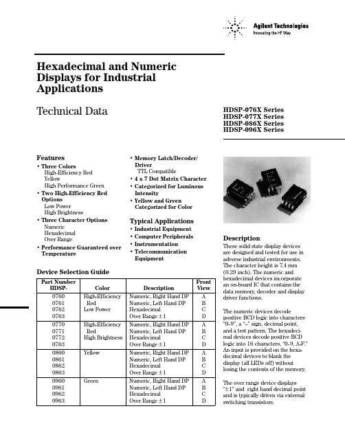
Hexadecimal and Numeric Displays for Industrial ApplicationsTechnical DataFeatures• Three ColorsHigh-Efficiency RedYellowHigh Performance Green• Two High-Efficiency Red OptionsLow PowerHigh Brightness• Three Character OptionsNumericHexadecimalOver Range• Performance Guaranteed over Temperature • Memory Latch/Decoder/ DriverTTL Compatible• 4 x 7 Dot Matrix Character • Categorized for Luminous Intensity• Yellow and Green Categorized for Color Typical Applications• Industrial Equipment• Computer Peripherals• Instrumentation• Telecommunication EquipmentDevice Selection GuidePart Number Front HDSP-Color Description View 0760High-Efficiency Numeric, Right Hand DP A0761Red Numeric, Left Hand DP B0762Low Power Hexadecimal C0763Over Range ±1D0770High-EfficiencyNumeric, Right Hand DP A 0771Red Numeric, Left Hand DP B 0772High Brightness Hexadecimal C 0763Over Range ±1D 0860Yellow Numeric, Right Hand DP A 0861Numeric, Left Hand DP B 0862Hexadecimal C 0863Over Range ±1D 0960Green Numeric, Right Hand DP A 0961Numeric, Left Hand DP B 0962Hexadecimal C 0963Over Range ±1D DescriptionThese solid state display devices are designed and tested for use in adverse industrial environments. The character height is 7.4mm (0.29 inch). The numeric and hexadecimal devices incorporate an on-board IC that contains the data memory, decoder and display driver functions.The numeric devices decode positive BCD logic into characters “0-9”, a “–” sign, decimal point, and a test pattern. The hexadeci-mal devices decode positive BCD logic into 16 characters, “0-9, A-F.”An input is provided on the hexa-decimal devices to blank the display (all LEDs off) without losing the contents of the memory. The over range device displays “±1” and right hand decimal point and is typically driven via external switching transistors.HDSP-076X SeriesHDSP-077X SeriesHDSP-086X SeriesHDSP-096X SeriesPackage DimensionsZAbsolute Maximum RatingsDescription Symbol Min.Max.Unit Storage Temperature, Ambient T S-65+100°C Operating Temperature, Ambient[1]T A-55+85°C Supply Voltage[2]V CC-0.5+7.0V Voltage Applied to Input Logic, dp and Enable Pins V I, V DP, V E-0.5V CC V Voltage Applied to Blanking Input[2]V B-0.5V CC V Maximum Solder Temperature at 1.59 mm (0.062 inch)260°C Below Seating Plane, t ≤ 5 secondsRecommended Operating ConditionsDescription Symbol Min.Nom.Max.Unit Supply Voltage[2]V CC 4.5 5.0 5.5V Operating Temperature, Ambient[1]T A-55+85°C Enable Pulse Width t W100nsec Time Data Must Be Held Before Positive t SETUP50nsec Transition of Enable LineTime Data Must Be Held After Positive t HOLD50nsec Transition of Enable LineEnable Pulse Rise Time t TLH 1.0msec Optical Characteristics at T A = 25°C, V CC = 5.0 VNotes:1. The nominal thermal resistance of a display mounted in a socket that is soldered onto a printed circuit board is RθJA = 50°C/W/device. The device package thermal resistance is RθJ-PIN = 15°C/W/device. The thermal resistance device pin-to-ambient through the PC board should not exceed 35°C/W/device for operation at T A = +85°C.2. Voltage values are with respect to device ground, pin 6.3. These displays are categorized for luminous intensity with the intensity category designated by a letter code located on the back ofthe display package. Case temperature of the device immediately prior to the light measurement is equal to 25°C.Electrical Characteristics; T A = -55°C to +85°CNotes:4. The luminous intensity at a specific operating ambient temperature, I V (T A ) may be approximated from the following exponential equation: I (T = I (25°C) e [k (T - 25°C)].d device.6. The HDSP-0860 and HDSP-0960 series devices are categorized as to dominant wavelength with the category designated by a number on the back of the display package.7. All typical values at V CC = 5.0 V and T A = 25°C.AOperational ConsiderationsElectricalThese devices use a modified4x7 dot matrix light emitting diode to display decimal/hexa-decimal numeric information. The high efficiency red and yellow LEDs are GaAsP epitaxial layer on a GaP transparent substrate. The green LEDs are GaP epitaxial layer on a GaP transparent substrate. The LEDs are driven by constant current drivers, BCD information is accepted by the display memory when the enable line is at logic low and the data is latched when the enable is at logic high. Using the enable pulse width and data setup and hold times listed in the Recommended Operating Conditions allows data to be clocked into an array of displays at a 6.7 MHz rate.The decimal point input is activelow true and this data is latchedinto the display memory in thesame fashion as the BCD data.The decimal point LED is drivenby the on-board IC.The blanking control input on thehexadecimal displays blanks (turnsoff) the displayed informationwithout disturbing the contents ofdisplay memory. The display isblanked at a minimum thresholdlevel of 2.0 volts. When blanked,the display standby power isnominally 250 mW at T A = 25°C.MechanicalThe primary thermal path forpower dissipation is through thedevice leads. Therefore, to insurereliable operation up to anambient temperature of +85°C, itis important to maintain a case-to-ambient thermal resistance ofless than 35°C watt/device asmeasured on top of display pin 3.For information on soldering andpost solder cleaning see Applica-tion Note 1027, Soldering LEDComponents.Contrast EnhancementThese display devices aredesigned to provide an optimumON/OFF contrast when placedbehind an appropriate contrastenhancement filter. For furtherinformation, please refer toApplication Note 1015, ContrastEnhancement Techniques forLED Displays.Over Range DisplayThe over range devices display“±1” and decimal point. Thecharacter height and packageconfiguration are the same as thenumeric and hexadecimaldevices. Character selection isobtained via external switchingtransistors and current limitingresistors.Package DimensionsNotes:0: Line switching transistor in Figure 7 cutoff.1: Line switching transistor in Figure 7 saturated.X: 'don't care'Absolute Maximum RatingsDescriptionSymbol Min.Max.Unit Storage Temperature, Ambient T S-65+100°C Operating Temperature, Ambient T A -55+85°C Forward Current, Each LED I F 10mA Reverse Voltage, Each LEDV R5VLuminous Intensity per LED[3,4]Figure 3. Typical Driving Circuit.Electrical Characteristics: T = -55°C to +85°CData subject to change.Copyright © 1999 Agilent Technologies, Inc. Obsoletes 5953-9395 (1/84)5963-7395E (11/99)。
最新HDS VSP G200安装配置指南资料
目录第一章产品概述 (2)1.1 产品简介 (2)1.2 型号升级 (2)1.3 主要指标 (2)1.4 高密度扩展柜 (3)1.5 RAID支持 (3)1.6 磁盘相关属性 (4)第二章存储外观说明 (4)2.1 外观说明 (4)2.2 设备安装 (5)2.3 控制器及SVP的IP地址说明 (6)第三章安装和配置SVP (8)3.1 登陆SVP (8)3.2 SVP前置面板说明 (10)3.3 重装管理工具Storage Device (11)3.4 微码更新 (12)第四章SNM2基本操作 (13)4.1 登录管理工具 (13)4.2 安装硬盘 (14)4.3Li ce n se管理 (18)4.4 在线微码升级 (19)4.5 创建热备盘 (20)4.6 删除热备盘 (22)4.7 端口设置 (23)4.8 RAID组划分 (25)4.9 创建LDEVS (26)4.10 Pool配置 (29)4.11 在pool上创建LDEVs (31)4.12 Host Group配置 (33)4.13 添加外部卷 (39)4.14 删除Pool (42)4.15 格式化LEDVS (45)4.16 ADD lUN PATHS 就是映射卷到主机 (47)4.17 删除LEDVs (48)4.18 删除PG(Raid)组 (49)4.19 删除外部卷 (50)4.20 修改网络端口参数 (52)4.21 其他操作 (53)4.22 修改时间 (59)4.23 Warning告警灯消除 (60)第五章MPC 的安装 (62)第六章硬件更换 (68)第七章HUS 110的卷映射给G200 (71)第一章产品概述1.1 产品简介HDS VSPGx00(Panama)系列主要包含以下几个产品:G200、G400、G600、G800,是HDS新一代中高端存储产品。
该系列产品统一运行的存储操作系统为SVOS。
1.2 型号升级存储产品的型号升级,主要是指G400到G600之间的升级,G400可通过购买升级license包及相应的硬件【前后端接口和内存】,可实现无中断应用在线升级到G600,从而提升存储系统的性能。
HDS VSP G200售后维护手册

1. G200基本功能介绍 2. G200日常维护操作
3. HDS售后工作流程
HDS售后工作流程
用户可随时播打7*24热线电话:400 678 6783
‒ 需要提供的以下信息 控制器的序列号:420721 客户名称信息及联系方式:京东方/138xxxxxxxx 故障信息:存储的日志或者截图信息 ‒ 用户可在4小时以内获得HDS二线工程师的响应
HDS售后工作流程
MPC luncher日志收集小工具
(启动密码:raid-mpc)
感谢&提问
2U x 12 2U: G200
4U: G400/600
2U x 24
磁盘笼模块
SSD (SFF) SAS (SFF)
NLSAS (LFF) SSD (SFF) SAS (SFF)
4U x 60 1U: SVP
管理服务器
3U: HNAS 4000 2U x 12
NAS模块
FMD (LFF)
VSP G系列软件概览_SVP管理服务器
Pool1:RAID5,约6TB容
量,规划存储虚拟机文件
RAID Level RAID5 RAID6 RAID1+0
硬盘配置支持范围 3D + 1P 、4D + 1P、6D + 1P、7D + 1P 6D + 2P 、12D + 2P、14D + 2P 2D + 2P、4D + 4P
G200售后维护手册
微码升级
微码升级选择GUM工具
点击Update之后,弹出以下界 面(事先需将微码文件解压出 来得到一个.mda文件)
点击“Apply”按钮之后弹出以下 界面
派尔高“D”协议中文
派尔高“D ”协议手册内容:这手册涵盖二个版本同轴(看下面) 协议和422/485协议的版本。
这两个版本的派尔高是被分为15位的(只固定速度) 版本和32位的(变化速度) 版本。
422/485版本增加一些结构为了异步媒体传输信号,并且在标有“数字的同轴”的部分加以解释。
这手册包含的协议是为说明同轴系列装备的和派尔高的 “D ” 版本接收器. 为了从一个控制器到平的和斜的接收驱动或视频上的摄像机传输控制信号,同轴是以派尔高的名字而出现的。
这个文件将从历史的角度陈述这一协议,因为协议的当前状况从进程的市郊更容易被理解。
起点(15比特同轴)同轴是脉冲宽度调整(PWM) 信号,被插入的到未用过的视频线(垂直的空白的间隔)。
2(s 脉冲表达1 而1 (s 脉冲表达0。
同轴最初以15 比特协议去控制远程装置的基本功能。
在视频信号的垂直空白间隔的18线,数据得以传输 区域的传输比特是:123456789101112131415BitS e n s eA u x 4A u x 3A u x 2A u x 1M a n A u t oO n O f fI r i s C l o s eI r i s O p e nF o c u s N e a r F o c u s F a rZ o o m W i d e Z o o m T e l eD o w nU pL e f tR i g h t在信息中,“感觉”字节决定下三个字节的功能,如果恰是感觉字节,那么下三个字节就反映Aux4,Aux2的状态,和人工浏览方式。
如果不是感觉字节, 那么下三个字节反映的情形是Aux3, Aux1, 和自动浏览方式。
例如, 在不是感觉字节下,你能控制自动浏览状态通过设置(开) 或清除(关) 字节4,如果感觉字节关而字节4开, 那么自动浏览是可以工作的,如果感觉字节是关和字节4是关,那么自动浏览是不能工作的 在这个协议下,我们很容易以同样的信息发出多种控制行为,例如, 在你打开了光圈和变焦镜头时,你能同时向上和左移动.第一扩充(扩充的15字节C OAXITRON )根据这一设置,新加了特征以允许远程装置记忆位置。
- 1、下载文档前请自行甄别文档内容的完整性,平台不提供额外的编辑、内容补充、找答案等附加服务。
- 2、"仅部分预览"的文档,不可在线预览部分如存在完整性等问题,可反馈申请退款(可完整预览的文档不适用该条件!)。
- 3、如文档侵犯您的权益,请联系客服反馈,我们会尽快为您处理(人工客服工作时间:9:00-18:30)。
DevicesPart Number HDSP-ColorDescriptionFront View0781High-Efficiency Red Numeric, Right Hand DP A 0782Low Power Numeric, Left Hand DP B 0783Over Range ±1C 0784HexadecimalD 0791High-Efficiency Red Numeric, Right Hand DP A 0792High Brightness Numeric, Left Hand DP B 0793Over Range ±1C 0794HexadecimalD 0881YellowNumeric, Right Hand DP A 0882Numeric, Left Hand DP B 0883Over Range ±1C 0884HexadecimalD 0981High-Performance GreenNumeric, Right Hand DP A 0982Numeric, Left Hand DP B 0983Over Range ±1C 0984HexadecimalDHDSP-078x HDSP-079x HDSP-088x HDSP-098xFeatures• Three Character Options Numeric, Hexadecimal, Over Range• Three ColorsHigh Efficiency Red, Yellow,High Performance Green• 4x 7 Dot Matrix Character • High Efficiency Red, Yellow and High Performance Green • Two High Efficiency Red OptionsLow Power, High Brightness • Performance Guaranteed Over Temperature• High Temperature Stabilized • Memory Latch/Decoder/DriverTTL Compatible• Categorized for Luminous IntensityDescriptionThese standard solid state displays have a 7.4 mm (0.29 inch) dot matrix character and an on-board IC with data memory latch/decoder and LED drivers in a glass/ceramic package.The hermetic HDSP-078x,-079x/-088x displays utilize a solder glass frit seal. The HDSP-098X displays utilize an epoxy glass-to-ceramic seal.The numeric devices decode posi-tive BCD logic into characters “0-9,” a “–” sign, decimal point,and a test pattern. Thehexadecimal devices decodeGlass/Ceramic Numeric and Hexadecimal Displays for Industrial Applications Technical Datapositive BCD logic into 16characters, “0-9, A-F.” An input is provided on the hexadecimal devices to blank the display (all LEDS off) without losing the contents of the memory.The over range device displays “±1” and right hand decimal point and is typically driven via external switching transistors.COUNTRY CODEPackage DimensionsAbsolute Maximum RatingsNotes:1. The nominal thermal resistance of a display mounted in a socket that is soldered onto a printed circuit board isRθJA=50°C/W/device. The device package thermal resistance is RθJ-PIN = 15°C/W/device. The thermal resistance device pin-to-ambient through the PC board should not exceed 35°C/W/device for operation up to T A = +100°C.2. Voltage values are with respect to device ground, pin 6.3. These displays are categorized for luminous intensity with the intensity category designated by a letter code located on the back ofthe display package. Case temperature of the device immediately prior to the light measurement is equal to 25°C.Electrical/Optical Characteristics T A = –55°C to +100°CNotes:4. The luminous intensity at a specific operating ambienttemperature, I v(T A), may be approximated from the following exponential equation: I v(T A)=I v(25°C) e[k(T-25°C)].Device KHDSP-078 Series–0.0131/°CHDSP-079x SeriesHDSP-088x Series–0.0112/°CHDSP-098x Series–0.0104/°C 5. The dominant wavelength, λd, is derived from the CIE chroma-ticity diagram and represents the single wavelength whichdefines the color of the device.6. The HDSP-088X and HDSP-098X series devices are categor-ized as to dominant wavelength with the category designated by a number on the back of the display package.7. All typical values at V CC = 5.0 V and T A = 25°C.Operational ConsiderationsElectricalThese devices use a modified4x7 dot matrix of light emitting diodes to display decimal/ hexadecimal numeric informa-tion. The high efficiency red and yellow displays use GaAsP/GaP LEDs and the high performance green displays use GaP/GaP LEDs. The LEDs are driven by constant current drivers, BCD information is accepted by the display memory when the enable line is at logic low and the data islatched when the enable is atlogic high. Using the enable pulsewidth and data setup and holdtimes listed in the RecommendedOperating Conditions allows datato be clocked into an array ofdisplays at a 6.7MHz rate.The decimal point input is activelow true and this data is latchedinto the display memory in thesame fashion as the BCD data.The decimal point LED is drivenby the on-board IC.The blanking control input on thehexadecimal displays blanks(turns off) the displayedinformation without disturbingthe contents of display memory.The display is blanked at aminimum threshold level of 2.0volts. When blanked, the displaystandby power is nominally 250mW at T A = 25°C.The ESD susceptibility of the ICdevices is Class A of MIL-STD-883 or Class 2 of DOD-STD-1686and DOD-HDBK-263.AMechanicalThese displays are hermetically sealed for use in environments that require a high reliability device. These displays are designed and tested to meet a helium leak rate of5x10-8cc/sec.These displays may be mounted by soldering directly to a printed circuit board or insertion into a socket. The lead-to-lead pin spacing is 2.54 mm (0.100 inch) and the lead row spacing is 15.24 mm (0.600 inch). These displays may be end stacked with 2.54 mm (0.100 inch) spacing between outside pins of adjacent displays. Sockets such as Augat 324-AG2D (3 digits) or Augat 508-AG8D (one digit, right anglemounting) may be used.The primary thermal path forpower dissipation is through thedevice leads. Therefore, to insurereliable operation up to anambient temperature of +100°C,it is important to maintain abase-to-ambient thermalresistance of less than35°C watt/device as measured ontop of display pin 3.For further information onsoldering and post soldercleaning, see Application Note1027, Soldering LEDComponents.PreconditioningThese displays are 100% pre-conditioned by 24 hour storage at125°C, at 100°C for the HDSP-098x Series.Contrast EnhancementThese display devices aredesigned to provide an optimumON/OFF contrast when placedbehind an appropriate contrastenhancement filter. For furtherinformation on contrastenhancement, see ApplicationNote 1015, ContrastEnhancement for LEDDisplays.Over Range DisplayThe over range devices display“±1” and decimal point. Thecharacter height and packageconfiguration are the same as thenumeric and hexadecimaldevices. Character selection isobtained via external switchingtransistors and current limitingresistors.Absolute Maximum RatingsDescription Symbol Min Max Unit Storage Temperature, Ambient T S–65+125°C Operating Temperature, Ambient T A–55+100°C Forward Current, Each LED I F10mA Reverse Voltage, Each LED V R5VPackage DimensionsLuminous Intensity per LED(Digit Average) at T= 25°C Figure 3. Typical Driving Circuit.Notes:0: Line switching transistor in Figure 7 cutoff.1: Line switching transistor in Figure 7 saturated.X: ‘don’t care.’Electrical Characteristics T A = –55°C to +100°CColor Bin Limits (Dominant Wavelength)Note:Bin categories are established for classification of products. Productsmay not be available in all bin categories. Please consult your localAgilent Technologies representative./semiconductorsFor product information and a complete list ofdistributors, please go to our web site.For technical assistance call:Americas/Canada: +1 (800) 235-0312 or(916) 788-6763Europe: +49 (0) 6441 92460China: 10800 650 0017Hong Kong: (+65) 6756 2394India, Australia, New Zealand: (+65) 6755 1939Japan: (+81 3) 3335-8152 (Domestic/Interna-tional), or 0120-61-1280 (Domestic Only)Korea: (+65) 6755 1989Singapore, Malaysia, Vietnam, Thailand,Philippines, Indonesia: (+65) 6755 2044Taiwan: (+65) 6755 1843Data subject to change.Copyright © 2004 Agilent Technologies, Inc.Obsoletes 5964-6390EJuly 14, 20045988-2261EN。