FM25L16_06中文资料
FM25L256铁电存储器数据手册pdf
Pre-Prபைடு நூலகம்duction
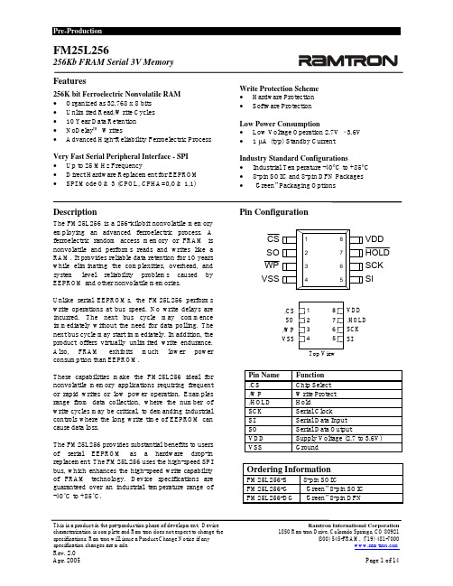
FM25L256
256Kb FRAM Serial 3V Memory
Features
256K bit Ferroelectric Nonvolatile RAM • Organized as 32,768 x 8 bits • Unlimited Read/Write Cycles • 10 Year Data Retention • NoDelay™ Writes • Advanced High-Reliability Ferroelectric Process
Instruction Decode Clock Generator Control Logic Write Protect
Instruction Register
8192 x 32 FRAM Array
Address Register
15
8
Counter
SI
Data I/O Register
SO
FM25CL64中文资料

RReevv 33..22
广州周立功单片机发展有限公司
地址:广州市天河北路 689 号光大银行大厦 12 楼 F4 网址:
广州周立功单片机发展有限公司
技术支持
如果您对文档有所疑问,您可以在办公时间(星期一至星期五上午 8:30~11:50;下午 1:30~5:30;星期六上午 8:30~11:50)拨打技术支持电话或 E-mail 联系。
传真:(0755)83793285
传真:(027)87163755
上海周立功
地址:上海市北京东路 668 号科技京城东座 7E 室 电话:(021)53083452 53083453 53083496 传真:(021)53083491
西安办事处
地址:西安市长安北路 54 号太平洋大厦 1201 室 电话:(029)87881296 83063000 87881295 传真:(029)87880865
3.2. 管脚描述.......................................................................................................................4 4. 概述 ...........................................................................................................................................5 5. 存储器结构 ...............................................................................................................................5 6. 串行外围接口-SPI 总线........................................................................................................6
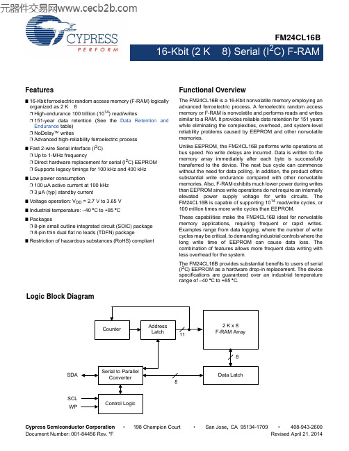
FM24CL16B中文资料
•
198 Champion Court
•
San Jose, CA 95134-1709
• 408-943-2600 Revised April 21, 2014
FM24CL16B
Contents
Pinouts .............................................................................. 3 Pin Definitions .................................................................. 3 Overview............................................................................ 4 Memory Architecture........................................................ 4 I2C Interface ...................................................................... 4 STOP Condition (P)..................................................... 4 START Condition (S)................................................... 4 Data/Address Transfer ................................................ 5 Acknowledge / No-acknowledge ................................. 5 Slave Device Address ................................................. 6 Addressing Overview (Word Address) ........................ 6 Data Transfer .............................................................. 6 Memory Operation............................................................ 6 Write Operation ........................................................... 6 Read Operation ........................................................... 7 Endurance ......................................................................... 8 Maximum Ratings............................................................. 9 Operating Range............................................................... 9 DC Electrical Characteristics .......................................... 9 Data Retention and Endurance ..................................... 10 Capacitance .................................................................... Thermal Resistance........................................................ AC Test Loads and Waveforms..................................... AC Test Conditions ........................................................ AC Switching Characteristics ....................................... Power Cycle Timing ....................................................... Ordering Information...................................................... Ordering Code Definitions ......................................... Package Diagrams.......................................................... Acronyms ........................................................................ Document Conventions ................................................. Units of Measure ....................................................... Document History Page ................................................. Sales, Solutions, and Legal Information ...................... Worldwide Sales and Design Support....................... Products .................................................................... PSoC® Solutions ...................................................... Cypress Developer Community................................. Technical Support ..................................................... 10 10 10 10 11 12 13 13 14 16 16 16 17 18 18 18 18 18 18FM2 NhomakorabeaCL16B
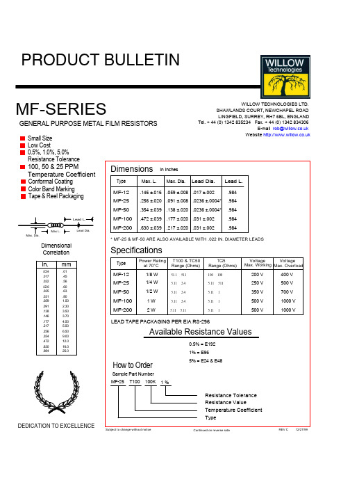
MF-25中文资料
MF-SERIESGENERAL PURPOSE METAL FILM RESISTORS Small SizePRODUCT BULLETIN REV C12/27/99Continued on reverse sideWILLOW TECHNOLOGIES LTD.SHAWLANDS COURT, NEWCHAPEL ROAD LINGFIELD, SURREY, RH7 6BL, ENGLANDTel. + 44 (0) 1342 835234 Fax. + 44 (0) 1342 834306E-mail rob@ Website REV D 1/20/99Characteristic Specificati on Test Method(All resistance measurements should be performed after stabilization or conditioning periods.) DC RESISTANCE Within specifiedtolerance.MIL-STD-202Method 303 TEMPERATURE COEFFICIENT As buyer requested±25PPM/°C ±100PPM/°C ±50PPM/°C ±200PPM/°C MIL-STD-202 Method 304DIELECTRIC STRENGTHNo flashover or damageMIL-STD-202 Method 3011/8W 300V 1 minute 1/4W 500V 1 minute 1/2W 700V 1 minute 1, 2W 750V 1 minute INSULATION RESISTANCE At least 1000M ΩMIL-STD-202 Method 302 100V 1 minute CURRENT NOISE TEST 5.11Ω to 9.99Ω less than 0.05µV/V10Ω to 9.99K Ω less then 0.1µV/V 10K Ω to 1M Ω less then 0.2µV/V MIL-STD-202 Method 308VIBRATION∆R within ±(0.25% + 0.05Ω)MIL-STD-202 Method 201 10~ HzX.Y.Z. 3 directions 2 hours each. TERMINAL STRENGTHNo broken or loosened terminals.MIL-STD-202 Method 211 RESISTANCE TO SOLDERING HEAT ∆R within ±(0.25% + 0.05Ω) MIL-STD-202 Method 210350°C, 3 ±0.05 seconds SOLDERABILITY At least 95% coverage MIL-STD-202 Method 208230°C, 5 seconds THERMAL SHOCK∆R within ±(0.5% + 0.05Ω)MIL-STD-202 Method 107 -55°C, +155°C 5 cyclesSHORT TIME OVERLOAD ∆R within ±(0.05% + 0.05Ω)MIL-R-10509 Para, 4.6.62.5 times rated working voltage, 5 seconds HUMIDITY∆R within ±(1% + 0.05Ω) NO mechanical damage MIL-STD-202 Method 10340°C, RH 95% 500 LOW TEMPERATURE OPERATION ∆R within ±(0.5% + 0.05Ω)MIL-R-10509 Para 4.6.5 Rated workingvoltage, @ -65°C 45 minutes. LOAD LIFE∆R within ±(1% + 0.05Ω)MIL-STD-202 Method 108 Rated workingVoltage 1 ½ hours on. ½ hour off for total 1000 hours RESISTANCE TO SOLVENT Color bands legible. No mechanical damage.MIL-STD-202 Method 2151.00.320.100.0320.0100.003101001K10K100K1M0-10-20-30-40-50Nominal Resistance (Ω)u V/VdBCURRENT NOISE。
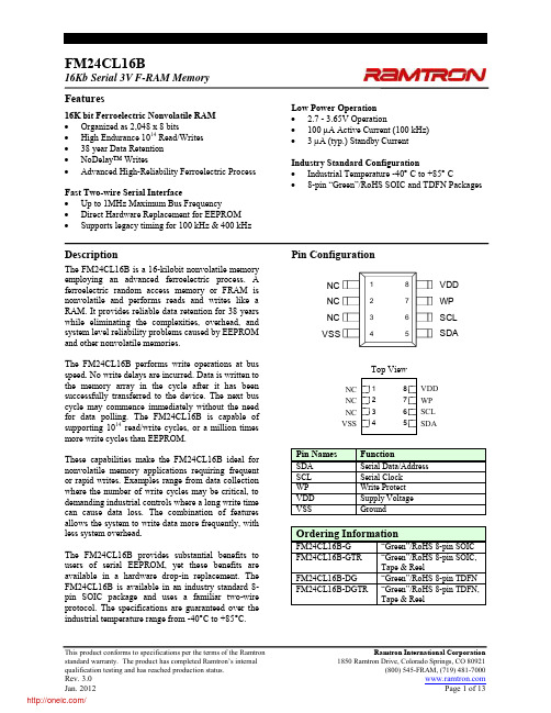
FM24CL16B-GTR;FM24CL16B-DGTR;FM24CL16B-DG;FM24CL16B-G;中文规格书,Datasheet资料
Two-wire Interface
The FM24CL16B employs a bi-directional two-wire bus protocol using few pins and little board space. Figure 2 illustrates a typical system configuration using the FM24CL16B in a microcontroller-based system. The industry standard two-wire bus is familiar to many users but is described in this section. By convention, any device that is sending data onto the bus is the transmitter while the target device for this data is the receiver. The device that is controlling the bus is the master. The master is responsible for generating the clock signal for all operations. Any device on the bus that is being controlled is a slave. The FM24CL16B is always a slave device. The bus protocol is controlled by transition states in the SDA and SCL signals. There are four conditions including Start, Stop, Data bit, and Acknowledge. Figure 3 illustrates the signal conditions that define the four states. Detailed timing diagrams are in the electrical specifications.
MEMORY存储芯片M25P16-VMC6TG中文规格书
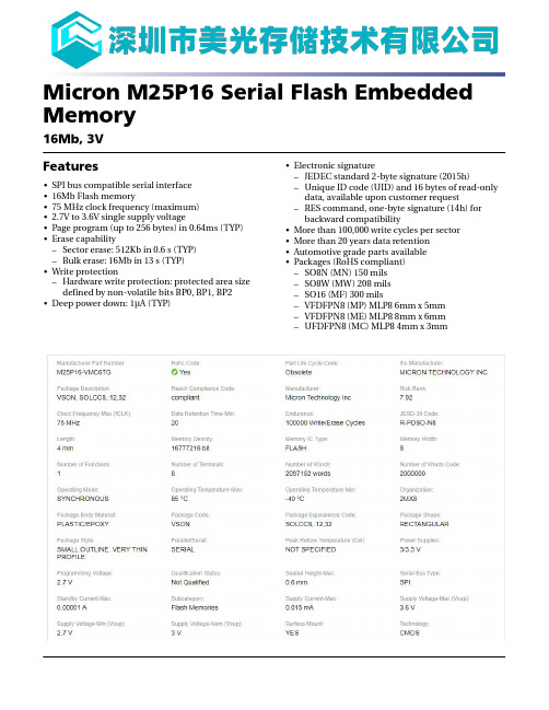
Micron M25P16 Serial Flash Embedded Memory16Mb, 3V Features•SPI bus compatible serial interface •16Mb Flash memory•75 MHz clock frequency (maximum)•2.7V to 3.6V single supply voltage•Page program (up to 256 bytes) in 0.64ms (TYP)•Erase capability–Sector erase: 512Kb in 0.6 s (TYP)–Bulk erase: 16Mb in 13 s (TYP)•Write protection–Hardware write protection: protected area size defined by non-volatile bits BP0, BP1, BP2•Deep power down: 1µA (TYP)•Electronic signature–JEDEC standard 2-byte signature (2015h)–Unique ID code (UID) and 16 bytes of read-only data, available upon customer request–RES command, one-byte signature (14h) for backward compatibility•More than 100,000 write cycles per sector •More than 20 years data retention •Automotive grade parts available •Packages (RoHS compliant)–SO8N (MN) 150 mils –SO8W (MW) 208 mils –SO16 (MF) 300 mils–VFDFPN8 (MP) MLP8 6mm x 5mm –VFDFPN8 (ME) MLP8 8mm x 6mm –UFDFPN8 (MC) MLP8 4mm x 3mmMicron M25P16 Serial Flash Embedded MemoryImportant Notes and WarningsFunctional DescriptionThe M25P16 is an 16Mb (2Mb x 8) serial Flash memory device with advanced write pro-tection mechanisms accessed by a high speed SPI-compatible bus. The device supports high-performance commands for clock frequency up to 75MHz.The memory can be programmed 1 to 256 bytes at a time using the PAGE PROGRAM command. It is organized as 32 sectors, each containing 256 pages. Each page is 256bytes wide. Memory can be viewed either as 8,192 pages or as 2,097,152 bytes. The en-tire memory can be erased using the BULK ERASE command, or it can be erased one sector at a time using the SECTOR ERASE command.This datasheet details the functionality of the M25P16 device based on 110nm process.Figure 1: Logic DiagramS#V CCHOLD#V SSDQ1C DQ0W#Table 1: Signal NamesMicron M25P16 Serial Flash Embedded MemoryFunctional DescriptionFigure 5: Bus Master and Memory Devices on the SPI BusSS2.Resistors (R) ensure that the memory device is not selected if the bus master leaves theS# line High-Z.3.The bus master may enter a state where all I/O are High-Z at the same time; for exam-ple, when the bus master is reset. Therefore, C must be connected to an external pull-down resistor so that when all I/O are High-Z, S# is pulled HIGH while C is pulled LOW.This ensures that S# and C do not go HIGH at the same time and that the t SHCH require-ment is met.4.The typical value of R is 100kΩ, assuming that the time constant R × C p (C p = parasiticcapacitance of the bus line) is shorter than the time during which the bus master leavesthe SPI bus High-Z.5.Example: Given that C p = 50pF (R × C p= 5μs), the application must ensure that the busmaster never leaves the SPI bus High-Z for a time period shorter than 5μs.质量等级领域:宇航级IC、特军级IC、超军级IC、普军级IC、禁运IC、工业级IC,军级二三极管,功率管等;应用领域:航空航天、船舶、汽车电子、军用计算机、铁路、医疗电子、通信网络、电力工业以及大型工业设备祝您:工作顺利,生活愉快!以深圳市美光存储技术有限公司提供的参数为例,以下为M25P16-VMC6TG的详细参数,仅供参考。
FM160中文资料

100
元器件交易网
RATING AND CHARACTERISTIC CURVES (FM120 THRU FM1100)
FIG.1-TYPICAL FORWARD CURRENT DERATING CURVE
AVERAGE FORWARD CURRENT,(A)
FIG.2-TYPICAL FORWARD CHARACTERISTICS
IR
C
SYMBOLS
MARKING CODE SS12 SS13 SS14 SS15 SS16 SS18 S110
V RRM
20 30 40 50 60 80
*1
V RMS
14 21 28 35 42 56 70
*2
VR
*3
VF
*4
Operating temperature (o C)
(V) FM120 FM130 FM140 FM150 FM160 FM180 FM1100
.1
Tj=25 C
.01
.05
.1
.5
1
5
10
50
100
.01 0
20
40
60
80
100 120 140
REVERSE VOLTAGE,(V)
PERCENT OF RATED PEAK REVERSE VOLTAGE,(%)
24
.01
.1
.3
.5
.7
.9
1.1
1.3
1.5
18
Tj=25 C 8.3ms Single Half Sine Wave JEDEC method
FORWARD VOLT AGE,(V)
SAP常用事务代码FI-MM

SAP常用事务代码FI-MM事务码描述(中英文)F.52 G/L: Acct Bal.Interest Calculation 总帐:计算科目余额利息F-06 Post Incoming Payments 收款记帐F-07 Post Outgoing Payments 付款记帐FB1S Clear G/L Account 结算总分类帐科目FB41 Post Tax Payable 应付税款记帐FBB1 Post Foreign Currency Valuation 外币评估记帐FBL3 Display G/L Account Line Items 显示总帐科目行项目FBL4 Change G/L Account Line Items 更改总分类帐科目的行项目FBX0 Change Documents for Ext.Documents 外部凭证的更改凭证FBX1 Post External Documents Received 收到外部凭证记帐FBX2 Change External Documents to be Sent 更改将送出的外部凭证FBX3 Display Extern.Documents to be Sent 显示将送出的外部凭证FBX4 Change External Documents Received 更改收到的外部凭证FBX5 Display External Documents Received 显示收到的外部凭证FBX6 Transfer: Extern.Documents to File 传输:外部凭证到文件FBX7 Load External Documents from File 从文件中装载外部凭证FS01 Create Master Record 创建主记录FS02 Change Master Record 更改主记录FS03 Display Master Record 显示主记录FS04 G/L Account Changes (Centrally) 总帐科目更改(集中地) FS05 Block Master Record 冻结主记录FS06 Mark Master Record for Deletion 把主记录标识为删除FS10 G/L Account Balance 总分类帐科目余额FSAA Display Address for Bal.Confirmatns 显示余额确认地址FSE2 Change Financial Statement Version 更改财务报表版本FSE3 Display Financial Statement Version 显示财务报表版本FSE4 Planning Preparation 计划准备FSE5 Maintain Planning 计划维护FSE6 Display Planning 显示计划FSE7 Maint.Bal.Sht/P+L Forgn Lang.T exts 维护资产负债表/利润表外语长文本FSE8 Display Forgn Lang.Bal.Sht/P+L Texts 显示外文的资产负债表/利润表文本FSE9 Automatic Balance Sheet/P+L Form 自动资产负债表/利润表FSM1 Create Sample Account 创建样本帐户FSM2 Change Sample Account 更改样本帐户FSM3 Display Sample Account 显示样本帐户FSM4 Sample Account Changes 样本科目更改FSM5 Delete sample account 删除样本科目FSMN 总帐菜单总帐菜单FSP1 Create Master Record in Chart/Accts 创建会计科目表中的主记录FSP2 Change master record in chart/accts 更改会计科目表中的主记录FSP3 Display Master Record in Chart/Accts 显示会计科目表的主记录FSP4 G/L Account Changes in Chart/Accts 会计科目表中的总帐科目变化FSP5 Block Master Record in Chart/Accts 冻结会计科目表中主记录FSP6 Mark Mast.Rec.for Del.in Chart/Accts 在科目表中的主记录上作标记以备删除FSS1 Create Master Record in Company Code 创建公司代码中的主记录FSS2 Change Master Record in Company Code 更改公司代码中的主记录FSS3 Display Master Record in Comp.Code 显示公司代码中的主记录FSS4 G/L Account Changes in Company Code 公司代码中的总帐科目修改FSSA Display Bal.Confirmatns Sel.Criteria 显示余额确认选择标准FSSP Change Bal.Confirmatns Sel.Criteria 改变余额确认选择标准FST2 Maintain Account Name 维护帐户名FST3 Display Account Name 显示帐户名GLT0 Flexible General Ledger 灵活的总帐GSP1 Allocation method 分摊方式GSP2 Line category 行类别GSP3 Business processes 业务处理GSP4 Determine line categories from acct 从科目的确定的目录行GSP5 Derive activity 引导业务GSP6 Define field control per ledger 每个分类帐定义字段控制GSP6GEN Doc split: Generation 明细凭证:生成GSP8 Doc. type assignment - process 凭证类型分配- 处理GSP9 Allocation Rule 分配规则GSPA Define account determination key 定义科目确定码GSPB Acct determination - posting key 科目确定- 过帐码GSPD Business processes 业务处理F.28 A/R: Reset Credit Limit 应收帐:重置信贷限额F.31 Credit Management - Overview 信贷管理—概览F.32 Credit Management - Missing Data 信贷管理—遗漏数据F.33 Credit Management - Brief Overview 信贷管理—简要概览F.34 Credit Management - Mass Change 信贷管理- 批变化F.35 Credit Master Sheet 贷方主表FD10 Customer Account Balance 客户科目余额FD11 Customer Account Analysis 客户帐户分析FD24 Credit Limit Changes 信贷限额变化FD32 Change Customer Credit Management 更改客户信贷管理FD33 Display Customer Credit Management 显示客户贷款管理FD37 Credit Management Mass Change 信贷管理批变化AR01 Call Up Asset List 调用资产清单AR02 Call Up Asset History Sheet 调用资产历史数据表AR03 Call Up Depreciation List 调用折旧清单AR04 Call Up Depreciation + Interest List 调用折旧+ 利息清单AR05 Call Up Asset Acquisition List 调用资产购置清单AR06 Call Up Asset Retirement List 调用资产报废清单AR07 Call Up Asset Transfer List 调用资产转帐清单AR08 Call Up Depreciation Compare List 调用折旧比较清单AR14 Call Up Manual Depreciation List 调用手工折旧清单AR18 Call Up Depr.Simulation 调用折旧模拟AR19 Call Up List of Origins 调用初始清单AR20 Retirement comparison 报废比较AR21 Mid-quarter Alert Report 季度中期警告报告AR22 Analysis of retirment revenue 报废收入的分析AR26 Call up special reserve list 调用特殊收入清单AR27 Call up: Group asset list 调用:集团公司资产清单AR28 Call up asset history 调用资产历史AR30 Display Worklist 显示工作清单AR32 Call-up create worklist 调用创建工作清单ARAL Display Application Log 显示应用程序日志ARQ0 FIAA - Ad hoc reports FIAA - Ad hoc 报告ART0 FIAA - Info system FI-AA:信息系统OA90 AM: Asset Register AM: 资产登记FM21 Change Original Budget 改变原预算FM22 Display Original Budget 显示原预算FM25 Change Supplement 改变补充FM26 Display Supplement 显示补充FM27 Change Return 改变返回FM28 Transfer Budget 转移预算FM29 Display Return 显示退回FM2E Change Budget Document 改变预算凭证FM2F Display Budget Document 显示预算文档FM2T Change Releases 更改下达FM2V Display Releases 显示下达FM98 Change Parked Document 更改暂存凭证FM9B Copy Budget Version 复制预算版本FM9D Lock Budget Version 锁定预算版本FM9E Unlock Budget Version 取消锁定预算版本FM9F Delete Budget Version 删除预算版本FM9G Roll Up Supplement 上滚补充FM9H Roll up Original Budget 累加原始预算FM9I Roll Up Return 累加返回FM9J Roll Up Releases 累加下达FM9K Change Budget Structure 更改预算结构FM9L Display Budget Structure 显示预算结构FM9M Delete Budget Structure 删除预算结构FM9N Generate Budget Object 生成预算对象FM9P Reconstruct Budget Distrbtd Values 重建预算分配值FM9Q Total Up Budget 预算汇总FMBV Activate Availability Control 激活有效性控制FMD1 Change Carryforward Rules 更改结转规则FMD2 Display Carryforward Rules 显示结转规则FMG1 FM: Create Commitment Item Group FM: 创建承诺项组FMG2 FM: Change Commitment Item Group FM: 更改承诺项组FMG3 FM: Display Commitment Item Group FM: 显示承诺项组FMG4 FM: Delete Commitment Item Group FM: 删除承诺项组FMG5 Generate BS Objects fr.Cmmt Item Grp 从承诺项组生成BS 对象FMP0 Maintain Financial Budget 维护财务预算FMP1 Display Financial Budget 显示财务预算FMP2 Delete Financial Budget Version 删除财务预算版本FR01 Change Original Commitments 更改原始承诺FR02 Display Original Commitments 显示原始承诺FR03 Original Commitments: Prel.Posting 初始承诺额:初步过帐FR04 Change Original Payments 更改原始收付FR05 Display Original Payments 显示原始收付FR07 Change Release Commitments 更改下达承诺FR08 Display Release Commitments 显示下达承诺FR10 Change Release Payments 更改下达收付FR11 Display Release Payments 显示下达收付FR13 Transfer Commitments 转帐承诺FR14 Transfer Payments 转帐收付FR15 Change Supplement Commitments 更改补充承诺FR16 Display Supplement Commitments 显示补充承诺FR17 Roll Up Supplement Commitments 上滚补充承诺FR19 Change Supplement Payments 更改补充收付FR20 Display Supplement Payments 显示补充收付FR21 Roll Up Supplement Payments 上滚补充收付FR23 Change Return Commitments 更改承诺申报表FR24 Display Return Commitments 显示退回承诺FR25 Roll Up Return Commitments 上滚申报表承诺FR27 Change Return Payments 更改收付申报表FR28 Display Return Payments 显示退回收付FR29 Returns: Roll-Up Payments 申报表:上滚收付FR32 Roll Up Budget Commitments 上滚预算承诺FR33 Roll Up Budget Payments 上滚预算收付FR34 Roll Up Commitment Releases 上滚承诺下达FR35 Roll Up Payment Releases 上滚收付发布====================================== =========================事务码描述(中英文)DPRL Change Material When Profile Deleted 删除参数文件时改变物料DPRV Change Material When Profile Changed 修改参数文件时修改物料MM00 物料主记录: 初始屏幕物料主记录: 初始屏幕MM01 Create Material - General 创建一般物料MM02 Change Material 改变物料MM03 Display Material 显示物料MM04 Display Material Change Documents 显示物料改变凭证MM06 Flag Material for Deletion 标出待删除物料MM11 Create Material (Schedule) 创建物料(计划)MM12 Change Material (Schedule) 修改物料(计划)MM13 Activate Planned Changes 计划中修改的激活MM14 Display Planned Changes 显示计划修改MM15 Display Changes (Migration) 显示变化(移动)MM16 Schedule Material for Deletion 将删除的计划物料MM18 Activate Planned Changes 计划中修改的激活MM19 Display Material at Key Date 显示关键日期时的物料MM60 Material Log 物料日志MM70 Sel. Materials Flagged for Deletion 标记为删除的选择物料MM71 Reorganize Materials 重组的物料MM73 Special Stocks: Preparation 特殊库存: 准备MM74 Archive Special Stocks 归档特殊库存MMAM Change Material Type 改变物料类型MMB1 Create Semifinished Product 创建半成品MMBE Stock Overview 库存总览MMD1 Create MRP Profile 建立MRP参数文件MMD2 Change MRP Profile 改变MRP参数文件MMD3 Display MRP Profile 显示MRP参数文件MMD6 Delete MRP Profile 删除MRP参数文件MMD7 Display MRP Profile Usage 显示MRP参数文件使用MMF1 Create Finished Product 创建产成品MMH1 Create Trading Goods 建立贸易货物MMI1 Create Operating Supplies Item 建立运行供应项目MMK1 Create Configurable Material 建立可设置物料MML1 Create Returnable Packaging 建立退货包装MMN1 Create Non-Stock Material 建立无库存物料MMNR Material Master Number Ranges 物料主文档的编号范围MMP1 Create Maintenance Assembly 建立维护组件MMPI Initialize Period 初始化期间MMPV Close Periods 结帐期间MMR1 Create Raw Material 建立原材料MMRV Allow Posting to Previous Period 允许对前期记帐MMS1 Create Service 生成服务MMSC Enter Storage Locations Collectively 汇总条目,库存地点MMU1 Create Non-Valuated Material 生成无价值物料MMV1 Create Packaging Material 建立有包装的物料MMVD Change Decentr. for Decentr.Shipping 改变为分散运输MMVH Create Centrally: Decentral.Shipping 集中建立: 分散发运MMVV Change Centr. for Decentr. Shipping 改变为集中式运货MMW1 Create Competitive Product 建立竞争性产品MMZ1 Create Material, General (Old MM01) 创建物料,一般的(旧的MM01)MMZ2 Change Material (Old MM02) 修改物料(旧的MM02)MMZ3 Display Material (Old MM03) 显示物料(旧的MM03)MP80 Create Forecast Profile 建立预测参数文件MP81 Change Forecast Profile 修改预测描述文件MP82 Delete Forecast Profile 删除预测参数文件MP83 Display Forecast Profile 显示预测参数文件MSC1 Create Batch 建立批量MSC2 Change Batch 改变批量MSC3 Display Batch 显示批量MSC4 Display Batch Changes 显示批量改变MSK1 Create Vendor Consignment Goods 创建供应商代销货物MSK2 Change Vendor Consignment Goods 改变供应商代销货物MSK3 Display Vendor Consignment Goods 显示供应商代销货物MSK4 Display Vdr Consignment Change Docs 显示供应商代销变动凭证MSK5 Vdr Consignment: Activate Fut. Price 供应商代销: 激活未来价格OMSL C MM-BD Maintain TMCNV C MM-BD 维护TMCNVOMY0 Display Material Transfer File 显示物料转移文件PPRL Change Material When Profile Deleted 删除参数文件时改变物料PPRV Change Material When Profile Changed 修改参数文件时修改物料W4EM Maintain No. Ranges for Weight EANs 维护加权EAN 的号码范围W4EN Maintain Number Ranges for EANs 维护EAN的号码范围W4EO SAN Maintenance SAN维护W4EQ Maintain EAN Prefixes 维护EAN前缀W4ES Maintain Number Range Categories 维护编号范围类别OLMS C RM-MAT Master Data Menu C RM-MAT 主数据菜单OMS1 Units of Measure Grouping 计量单位组OMS2 C MM-BD Material Types C MM-BD 物料类型OMS3 Configure Industry Sectors 设置行业部门OMS4 C MM-BD Material Status C MM-BD 物料类型OMS5 C MM-BD Set Up Laboratory C MM-BD 设置库OMS6 C MM-BD Storage Condition(s) C MM-BD 库存条件OMS7 C MM-BD Temperature Condition(s) C MM-BD 温度条件OMS8 C MM-BD Container Requirement(s) C MM-BD 集装箱需求OMS9 Configure Field/Screen Selection 配置字段/屏幕选择OMSA C MM-BD T130W Plant-Specific C MM-BD T130W工厂-特定OMSD C MM-BD F. Sel. Spec. T148G C MM-BD 工厂选择指定T148GOMSE C MM-BD F. Sel. Reference T148W C MM-BD 工厂选择参考T148WOMSF C MM-BD Material Groups C MM-BD 物料组OMSH C MM-BD Matchcode for Material C MM-BD 匹配码: 物料OMSM CS MM Set Up Administrative Data CS MM设置管理数据OMSN C MM-BD User Maintenance C MM-BD 用户维护OMSO C MM-BD User Profiles C MM-BD 用户参数文件OMSR C MM-BD Field Groups C MM-BD 字段组OMSS C MM-BD Field Groups: Special Stocks C MM-BD 字段组: 特殊库存OMST C MM-BD Record Layout f. BATCH INPUT C MM-BD 有关批量输入的记录格式OMSU C MM-BD Mat. Master Data Transfer C MM-BD 物料主记录数据的转换OMSW C MM-BD Record Layout f. BATCH INPUT C MM-BD 有关批量输入的记录格式OMSY C MM-BD Company Code for Matl Master 物料主记录的C MM-BD公司代码OMSZ C MM-BD Authorizations 设置MM-BD授权OMT0 C MM-BD Global Setting C MM-BD 全局设置OMT5 Auth. Group MatMaster (Inactive) 物料主文档授权组(非活动的)OMT7 Mat.Master Cust.-Specific Structures 物料主顾客-特定结构OMT8 Transfer Material Master Data by DI 按DI转移材料主数据OMY1 Create Input File from Material 创建来自物料的输人文件MM50 List Extendable Materials 列示可扩展物料MM51 List Extendable Materials (Old) 列出可扩展的物料(旧的)MM72 Display Archive of Materials 显示物料归档MM75 Display Archive of Special Stocks 显示特别库存归档MM90 Analyze ALE Appl. Log for MatMaster 为物料主文挡分析ALE应用程序日志MMDE Delete All Materials 删除所有物料OMT2 Required Fields Control MM-BD ALE/DI 要求字段控制MM-BD ALE/DIOMT3 Customizing for the Material Master 物料主文档的用户化OMT4 Customizing for EAN Messages 为EAN消息定制BD10 Send Material 发送物料BD11 Fetch Material 打开物料MAL1 Create material via ALE 通过ALE 创建物料MAL2 Change material via ALE 通过ALE 更改物料MM91 Delete ALE Appl. Log for Matl Master 为物料管理删除ALE应用程序日志MGW0 Maintain components for set product 为设置产品维护组件MGW1 Display components for set product 显示设置产品的部件MGW2 Maintain components for display art. 维护物品显示组件MGW3 Display components for display art. 显示物品显示的部件MGW4 Maintain components for lot article 维护批次物品的组件MGW5 Display components for lot article 显示批量物品的部件MGW6 Maintain components for empties art. 维护空物品的组件MGW7 Display components for empties art. 显示空物品的部件MM41 Create Material 创建物料MM42 Change Material 改变物料MM43 Display Material 显示物料MM44 Display Change Documents 显示更改文档RWBE Stock Overview 库存总览W4E5 Maintain No. Ranges 5-Fig. Wt EANs 维护号码范围5-指标Wt EANs WRST Transfer Master Data for Matl Maint. 物料维护的传输主数据OW01 Ref. plant per distribution chain 每个分销链的参考工厂BD14 Send vendor 发送供应商BD15 Open vendor 打开供应商M-01 Create vendor 创建供应商M-02 Create goods vendor 创建货物供应商M-03 Create payment recipient 创建付款的接收人M-04 Create invoicing party 创建发票部分M-05 Create carrier 创建载体M-06 Create ordering address 创建订单地址M-07 Create one-time vendor 创建一次性供应商M-12 Create hierarchy nodes 创建层次节点M-51 Create vendor 创建供应商M-52 Create goods vendor 创建货物供应商M-53 Create payment recipient 创建付款的接收人M-54 Create invoicing party 创建发票部分M-55 Create carrier 创建载体M-56 Create ordering address 创建订单地址M-57 Create one-time vendor 创建一次性供应商M-62 Create hierarchy nodes 创建层次节点MAP1 Create contact person 创建联系人MAP2 Change contact person 修改联系人MAP3 Display contact person 显示联系人MK12 Change vendor (Purchasing), planned 修改供应商(购买),计划的MK14 Planned vendor change (Purchasing) 计划修改供应商(购买)MK18 Activate planned vendor changes (Pu) 激活计划修改供应商(购买)MK19 Display vendor (purchasing), future 显示供应商(购买),将来MKH1 Maintain vendor hierarchy 维护供应商层次MKH2 Display vendor hierarchy 显示供应商层次MKH3 Activate vendor master (online) 激活供应商主档(联机)MKH4 Activate vendors (batch input) 激活供应商(批输入)MPE1 Create buyer 创建买主MPE2 Change buyer 修改买主MPE3 Display buyer 显示买主OMKC C MM PUR Price Marking 取消MM PUR 价格标记OMKD C MM PUR Supply Regions 取消MM PUR 供货区OMSG Account Groups: Vendor 科目组: 供应商OMSI C MM-BD Matchcode for vendor 供应商的C MM-BD 匹配码OMSJ C MM-BD Number Range for Vendor C MM-BD 号范围: 供应商OMSX TCODE/Field Selection: Vendor 事务码/字段选择: 供应商WBG1 Maintenance 维护WL00 Vendor Master 供应商主数据WOPS Partner Schema Assignment, Vendor 业务往来方案分配,供应商WYC1 Price Marking Agreement 价格标记协议WYL1 Batch input interface, vendors 批输入接口,供应商WYRL Vendor for returns 退货供应商XK07 Change vendor account group 修改供应商科目组BD30 Distribute material object list 分配物料对象清单BD31 Distribute document object list 分配凭证对象清单BD32 Distribute plant allocations(matBOM) 分布工厂分配(matBOM) CS00 BOM Menu BOM 菜单CS01 Create Material BOM 生成物料BOMCS02 Change Material BOM 更改物料BOMCS03 Display Material BOM 显示物料BOMCS05 Change Material BOM Group 更改物料BOM 组CS06 Display Material BOM Group 显示物料BOM 组CS07 Allocate Material BOM to Plant 分配物料BOM 到工厂CS08 Change Material BOM - Plant Alloc. 更改物料BOM - 工厂分配CS09 Display Allocations to Plant 显示到工厂的分配CS11 Display BOM Level by Level 逐层显示BOMCS12 Multi-level BOM 多层BOMCS13 Summarized BOM 汇总BOMCS14 BOM Comparison BOM 比较CS15 Single-Level Where-Used List 单层反查清单CS20 Mass Change: Initial Screen 大量更改: 初始屏幕CS21 Mass Material Change: Initial Screen 大量物料更改: 初始屏幕CS22 Mass Document Change: Initial Screen 大量文档更改: 初始屏幕CS23 Mass Class Change: Initial Screen 大量类更改: 初始屏幕CS24 Reorganize BOMs: Initial Screen 重组BOM : 初始屏幕CS25 Archiving for BOMs BOMs 的归档CS26 BOM deletion BOM删除CS27 Retrieval of BOMs BOM 检索CS31 Create class BOM 创建类BOMCS32 Change class BOM 改变类BOMCS33 Display class BOM 显示类BOMCS40 Create Link to Configurable Material 生成与可配置物料的链接CS41 Change Material Config. Allocation 更改物料配置分配CS42 Display Material Config. Allocation 显示物料配置分配CS51 Create Standard BOM 创建标准BOMCS52 Change Standard BOM 更改标准BOMCS53 Display Standard BOM 显示标准BOMCS61 Create Sales Order BOM 创建销售订单BOMCS62 Change Sales Order BOM 更改销售订单BOMCS63 Display Sales Order BOM 显示销售订单BOMCS71 Enqueue Test for Dialog RFC 对话RFC 的入队测试CS72 Current Settings 当前的设置CS80 Change Documents for Material BOM 更改物料BOM 文档CS81 Change Documents for Standard BOM 更改标准BOM 文档CS82 Change Documents for Sales Order BOM 更改销售订单BOM 的文档CS90 Material BOM Number Ranges 物料BOM 编号范围CS91 Number Ranges for Standard BOMs 标准BOMs 的编号范围CS92 Number Ranges for Sales Order BOMs 销售订单BOMs 的编号范围CSC5 Single-level where-used for classes 单层类反查CSD5 Single-level where-used for document 单层文档反查清单CV11 Create Document Structure 创建文档结构CV12 Change Document Structure 更改文档结构CV13 Display Document Structure 显示文档结构CV15 Change Document BOM Group 更改文档BOM 组CV16 Display Document BOM Group 显示文档BOM 组CV80 Change Documents for Doc. Structure 更改文档结构的文档CV91 Number Ranges for Doc. Structures 文档结构的编号范围OS42 Process Transfer File 处理传送文件OS43 Copy BOM changes 拷贝BOM 更改OS44 Copy BOM variants 拷贝BOM 变式OS45 Copy BOM with description 拷贝有描述的BOMOS46 Edit transfer file (long text)_ 编辑转换文件(长文本)OST1 CS Transport C Tables TCS21/TCS22 CS 传输C 表TCS21/TCS22 OST2 CS Transport C T ables BOM Usage CS 传输C 表格BOM 使用OST3 Transp. Customizing tabs T418F,T418G 传输用户化表T418F,T418G OS11 Spare Part Indicators 备件指示符OS12 Material Provision Indicators 物料供应标志OS13 Item Categories 项目类别OS14 Material Types Allowed in BOM Item 在BOM 项中允许的物料类型OS15 Variable-Size Item Formulas 可变尺寸项目公式OS16 BOM Item Object Type BOM 项目对象类型OS17 Explosion Types 展开类型OS18 Relevancy to costing 与成本计算相关OS20 BOM Usage BOM 用途OS21 BOM Usage Default Values 物料清单使用缺省值OS22 Copying Defaults for Item Statuses 复制项目状态的默认值OS23 BOM Statuses BOM 状态OS24 Material Types Allowed in BOMs 在BOM 中允许的物料类型OS25 BOMs with History Requirement 带历史需求的BOM OS26 Laboratory/Office 实验室/办公室OS27 Modification Parameters for BOMs 用于BOM 的修改参数OS28 Defaults for BOMs BOM 的默认值OS29 User-Specific Settings for BOMs 特定用户的BOM表设置OS30 Application 应用OS31 BOM Usage Priorities BOM 使用优先级OS32 Alternative BOM Determination 替代BOM 确定OS33 Alt. Determination in Inventory Mgmt 库存管理中的替代确定OS34 Alt. Determination in Costing 成本核算中的替代确定OS35 Alt. Determination in Production 生产中的替代确定OS36 Alt. Determination in SD SD 中的替代确定OS37 Alt. Determination in PM PM 中的替代确定OS38 Alt. Determination in MRP MRP 中的替代确定OS40 Generate BOM Transfer File 生成BOM 传送文件OS41 Transfer BOM without Long T ext 传送不带长文的BOM OS47 Field Groups: Assigned Fields 字段组:分配字段OS48 Field Groups: Definition and Descs 字段组:定义和说明OS57 Document Revision Level Sequence 文档修改级别顺序OS70 User-Specific List Profiles 特定用户的列表描述文件OSSZ C PP Authorizations C PP 授权ME00 采购功能采购功能ME01 Maintain Source List 维护货源清单ME03 Display Source List 显示货源清单ME04 Changes to Source List 改变货源清单ME05 Generate Source List 生成货源清单ME06 Analyze Source List 分析货源清单ME07 Reorganize Source List 重组货源清单ME08 Send Source List 发送源清单ME0M Source List for Material 物料的资源清单ME11 Create Purchasing Info Record 建立采购信息记录ME12 Change Purchasing Info Record 改变采购信息记录ME13 Display Purchasing Info Record 显示采购信息记录ME14 Changes to Purchasing Info Record 改变采购信息记录ME15 Flag Purch. Info Rec. for Deletion 为删除标记采购信息记录ME16 Purchasing Info Recs. for Deletion 要删除的采购信息记录ME17 Archive Info Records 归档信息记录ME18 Send Purchasing Info Record 发送采购信息记录ME1A Archived Purchasing Info Records 归档的采购信息记录ME1B Redetermine Info Record Price 重新确定信息记录价格ME1E Quotation Price History 报价价格的历史记录ME1L Info Records Per Vendor 每供应商的信息记录ME1M Info Records Per Material 每物料的信息记录ME1P Purchase Order Price History 采购订单价格历史记录ME1W Info Records Per Material Group 每物料组的信息记录ME1X Buyer's Negotiation Sheet for Vendor 用于供应商的买方采购谈判记录ME1Y Buyer's Negotiat. Sheet for Material 买方物料采购谈判记录表ME21 Create Purchase Order 建立采购订单ME22 Change Purchase Order 改变采购订单ME23 Display Purchase Order 显示采购订单ME24 Maintain Purchase Order Supplement 维护采购订单补充ME25 Create PO with Source Determination 生成带决定货源的订单ME26 Display PO Supplement (IR) 显示采购订单补充(IR)ME27 Create Stock Transport Order 建立库存运输订单ME28 Release Purchase Order 批准采购订单ME2A Monitor Confirmations 监视确认ME2B POs by Requirement Tracking Number 需要追踪号的采购订单ME2C Purchase Orders by Material Group 按物料组分类采购订单ME2J Purchase Orders for Project 项目的采购项目ME2K Purch. Orders by Account Assignment 采购订单帐户设置ME2L Purchase Orders by Vendor 按供应商分类采购订单ME2M Purchase Orders by Material 按物料分类采购订单ME2N Purchase Orders by PO Number 按订单号分类采购订单ME2O SC Stock Monitoring (Vendor) SC 库存监视(供应商)ME2V GR Forecast 收货预测ME2W Purchase Orders for Supplying Plant 供货工厂的采购订单ME31 Create Outline Agreement 创建框架协议ME31K Create Contract 创建合同ME31L Create Scheduling Agreement 创建计划协议ME32 Change Outline Agreement 更改框架协议ME32K Change Contract 修改合同ME32L Change Scheduling Agreement 修改计划协议ME33 Display Outline Agreement 显示框架协议ME33K Display contract 显示合同ME33L Display Scheduling Agreement 显示计划协议ME34 Maintain Outl. Agreement Supplement 维护框架协议补充ME34K Maintain Contract Supplement 维护合同附录ME34L Maintain Sched. Agreement Supplement 维护计划协议附录ME35 Release Outline Agreement 批准框架协议ME35K Release Contract 发放合同ME35L Release Scheduling Agreement 发放计划协议ME36 Display Agreement Supplement (IR) 显示协议补充(IR) ME37 Create Transport Scheduling Agmt. 创建运输计划协议ME38 Maintain Sched. Agreement Schedule 维护计划协议计划ME39 Display Sched. Agmt. Schedule (TEST) 显示计划协议计划(测试) ME3A Transm. Release Documentation Record 传输发放文档记录ME3B Outl. Agreements by Req. Tracking No 根据申请轨迹号的框架协议ME3C Outline Agreements by Material Group 按物料组的草案协议ME3J Outline Agreements for Project 项目的框架协议ME3K Outl. Agreements by Acct. Assignment 根据帐户设置的框架协议ME3L Outline Agreements by Vendor 根据供应商的框架协议ME3M Outline Agreements by Material 根据物料的框架协议ME3N Outline Agreements by Agreement No. 根据协议号的框架协议ME3P Recalculate Contract Price 重定合同价ME3R Recalculate Sched. Agreement Price 重新计算计划协议价格ME41 Create Request For Quotation 建立询价ME42 Change Request For Quotation 改变询价ME43 Display Request For Quotation 显示询价ME44 Maintain RFQ Supplement 维护询价补充ME45 Release RFQ 批准RFQME47 Create Quotation 创建报价ME48 Display Quotation 显示报价ME49 Price Comparison List 价格比较清单ME4B RFQs by Requirement Tracking Number 按需求跟踪号的询价ME4C RFQs by Material Group 按物料组的询价ME4L RFQs by Vendor 按供应商的询价ME4M RFQs by Material 按物料的询价ME4N RFQs by RFQ Number 按询价号的询价ME4S RFQs by Collective Number 按集中号的询价ME51 Create Purchase Requisition 建立采购申请ME52 Change Purchase Requisition 改变采购请求ME53 Display Purchase Requisition 显示采购申请ME54 Release Purchase Requisition 批准采购请求ME55 Collective Release of Purchase Reqs. 采购请求的集中批准ME56 Assign Source to Purch. Requisition 对采购申请分配供货源ME57 Assign and Process Requisitions 分配和处理申请ME58 Ordering: Assigned Requisitions 订单: 分配的请求ME59 Automatic Generation of POs 采购订单的自动生成ME5A Purchase Requisitions: List Display 采购申请: 清单显示ME5F Release Reminder: Purch. Requisition 批准催单:采购申请ME5J Purchase Requisitions for Project 项目的采购需求ME5K Requisitions by Account Assignment 按帐户设置分类的采购申请ME5R Archived Purchase Requisitions 归档的采购申请ME5W Resubmission of Purch. Requisitions 采购申请的重述ME80 Purchasing Reporting 采购报告ME80A Purchasing Reporting: RFQs 采购报表: 询价ME80F Purchasing Reporting: POs 采购报表: 采购订单ME80R Purchasing Reporting: Outline Agmts. 采购报表: 草案协议ME81 Analysis of Order Values 订单价值分析ME82 Archived Purchasing Documents 归档的采购凭证ME84 Generation of Sched. Agmt. Releases 计划协议发放的生成ME85 Renumber Schedule Lines 重新给计划行编号ME86 Aggregate Schedule Lines 聚集计划行ME87 Aggregate PO History 聚集采购清单历史记录ME90 Message Processing for Purch. Docs. 采购凭证的信息处理ME91 Purchasing Docs.: Urging/Reminding 采购凭证: 催货/催付ME91A Urge Submission of Quotations 报价的紧急提交ME91E Sch. Agmt. Schedules: Urging/Remind. 计划协议计划: 紧急/余额ME91F Purchase Orders: Urging/Reminders 采购订单: 紧急/余额ME92 Monitor Order Acknowledgment 监控订单认可ME92F Monitor Order Acknowledgment 监控订单认可ME92K Monitor Order Acknowledgment 监控订单认可ME92L Monitor Order Acknowledgment 监控订单认可ME97 Archive Purchase Requisitions 归档采购凭证ME98 Archive Purchasing Documents 归档采购凭证ME99 Messages from Purchase Orders 来自采购订单的消息ME9A Message Output: RFQs 消息输出: 询价ME9E Message Output: Sch. Agmt. Schedules 消息输出: 计划协议计划ME9F Message Output: Purchase Orders 消息输出: 采购订单ME9K Message Output: Contracts 消息输出: 合同ME9L Message Output: Sched. Agreements 消息输出: 计划协议MEAN Delivery Addresses 供货地址MEIS Intrastat Selection: Arrivals 州内选择: 到达MEK0 Conditions, Purchasing: Customizing 条件,采购: 客户设置MEK1 Create Conditions (Purchasing) 建立条件(采购)MEK2 Change Conditions (Purchasing) 改变条件(采购)MEK3 Display Conditions (Purchasing) 显示条件(采购)MEK4 Create Conditions (Purchasing) 建立条件(采购)MEKA Conditions: General Overview 条件: 一般的总览MEKB Conditions for Contract 合同的条件MEKC Conditions for Info Record 信息记录的条件MEKD Conditions for Material Group 物料组的条件MEKE Conditions for Vendor 供应商的条件MEKF Conditions for Material Type 物料类型的条件MEKG Conditions for Conditions Group 条件组的条件MEKH Market Price 市场价格MEKI Conditions for Incoterms 国际贸易条件MEKJ Conditions for Invoicing Party 出票方的条件MEKK Conditions for Vendor Sub-Range 供应商子范围的条件MEKL Price Change: Scheduling Agreements 价格修改:计划协议MEKLE Currency Change: Sched. Agreements 货币改变: 计划协议MEKP Price Change: Info Records 价格变化,信息记录MEKPE Currency Change: Info Records 货币改变: 信息记录MEKR Price Change: Contracts 价格变化,合同MEKRE Currency Change: Contracts 货币改变: 合同MEKX Transport Condition Types Purchasing 传送采购条件类型MEKY Trnsp. Calc. Schema: Mkt. Pr. (Pur.) 传送定价纲要:市场价格(采购) MEKZ Trnsp. Calculation Schemas (Purch.) 传送定价纲要(采购)MELB Purch. Transactions by Tracking No. 采购交易跟踪号MEPA Order Price Simulation/Price Info 订单价格模拟/价格信息MEPB Price Info/Vendor Negotiations 价格信息/供应商谈判MEQ1 Maintain Quota Arrangement 维护配额协议MEQ3 Display Quota Arrangement 显示配额的协议MEQ4 Changes to Quota Arrangement 改变配额协议MEQ6 Analyze Quota Arrangement 分析配额协议MEQ7 Reorganize Quota Arrangement 重组配额协议MEQ8 Monitor Quota Arrangements 监视配额的协议MEQB Revise Quota Arrangement 重设配额协议MEQM Quota Arrangement for Material 物料的配额协议MKVG Settlement and Condition Groups 结算和条件组MKVZ List of Vendors: Purchasing 供应商清单: 采购MKVZE Currency Change: Vendor Master Rec. 货币改变: 供应商主记录MN01 Create Message: RFQ 建立信息: 询价MN02 Change Message: RFQ 改变信息: 询价MN03 Display Message: RFQ 显示信息: 询价MN04 Create Message: PO 建立信息: 采购订单MN05 Change Message: PO 改变信息: 采购订单MN06 Display Message: PO 显示信息: 采购订单MN07 Create Message: Outline Agreement 建立信息: 框架协议MN08 Change Message: Outline Agreement 改变信息: 框架协议MN09 Display Message: Outline Agreement 显示信息: 框架协议MN0Z Set Up Message Determination 设置信息确认MN10 Create Message: Schd. Agmt. Schedule 建立消息: 计划协议计划MN11 Change Message: Schd. Agmt. Schedule 改变消息: 计划协议计划MN12 Displ. Message: Schd. Agmt. Schedule 显示消息: 计划协议计划MN24 Create Message: Shipping Notif. 创建消息: 装运通知MN25 Change Message: Shipping Notif. 修改消息: 装运通知MN26 Display Message: Shipping Notif. 显示消息: 装运通知MP01 Maintain AMPL records 维护AMPL 记录MP02 Maintain AMPL records 维护AMPL 记录OMEV Determine Consgt. Valuation Prices 确定寄售估价价格OMGT Import data 输入数据OMH4 C MM PUR Item Categories C MM PUR 项目类别OMH5 Default Doc. Type in Transactions 在事务处理中的缺省的凭证类型OMJO Convert MKOP into Consgt. Info Recs. 转换MKOP 到寄售信息记录OMJP Batch Input: Consignment Info Recs.批量输入: 寄售信息记录OMJQ Deletion Flag: Consg. Price Segments 删除标志: 寄售价格段OMPN C MM-PUR Purchasing Manuf. Part No. C MM-PUR 采购制造商零件编号OMQ1 Transfer of purchase orders 采购订单的传输OMQ2 Transfer of PO history PO 历史的传输OMQ3 Transfer of PO texts PO 文本的传输OMQ4 Create PO transfer file 创建PO 传输文件OMQ5 Edit PO transfer file 编辑PO 传输文件OMQ6 Create PO text transfer file 创建PO 文本传输文件OMUP Forecast Schedule: Transm. Profile 预测计划: 传输参数文件OMXX Contract release docu. updating MM 合同下达凭证更新MMOMZ1 Partner Role Definition: Purchasing 合伙角色定义: 采购OMZ2 Key Reassignment: Partner Roles 码重设: 合伙角色OMZ3 Admissible Partner Roles: Acc. Group 可接受合伙角色: 科目组OMZ4 Partner Schemas: Vendor Master 合伙方案: 供应商主记录OMZ5 Assignment of Schemas to Acc. Groups 给科目组设置方案OMZ6 Partner Schemas: Purch. Documents 合伙方案: 采购凭证OMZ7 Assignment of Schemas to Doc. Types 给凭证类型设置方案OMZ8 Partner Schemas: Rebate Arrangements 合作伙伴概要: 回扣安排OMZ9 Assign Schemas to Arrangement Types 把概要分配给。
FM25Q16中文资料
9. 10.
BLOCK DIAGRAM...........................................................................................................................10 FUNCTION DESCRIPTION.............................................................................................................11 10.1 SPI OPERTATIONS.......................................................................................................11 10.1.1 10.1.2 10.1.3 10.1.4 10.2 10.2.1 Standard SPI Instructions...............................................................................11 Dual SPI Instructions......................................................................................11 Quad SPI Instructions.....................................................................................11 Hold Function.................................................................................................11 Write Protect Features ................................................................................12 ...........................................................................13
FM25L256中文资料

CS
1
SO
2
WP
3
VSS
4
8
VDD
7
1 SO 2 /WP 3 VSS 4
8 VDD 7 /HOLD 6 SCK 5 SI
Top View
Pin Name /CS /WP /HOLD SCK SI SO VDD VSS
Function Chip Select Write Protect Hold Serial Clock Serial Data Input Serial Data Output Supply Voltage (2.7 to 3.6V) Ground
Ramtron International Corporation 1850 Ramtron Drive, Colorado Springs, CO 80921
(800) 545-FRAM, (719) 481-7000
Page 1 of 14
元器件交易网
The FM25L256 provides substantial benefits to users of serial EEPROM as a hardware drop-in replacement. The FM25L256 uses the high-speed SPI bus, which enhances the high-speed write capability of FRAM technology. Device specifications are guaranteed over an industrial temperature range of -40°C to +85°C.
Unlike serial EEPROMs, the FM25L256 performs write operations at bus speed. No write delays are incurred. The next bus cycle may commence immediately without the need for data polling. The next bus cycle may start immediately. In addition, the product offers virtually unlimited write endurance. Also, FRAM exhibits much lower power consumption than EEPROM.
FM25L16B铁电存储SPI操作例程
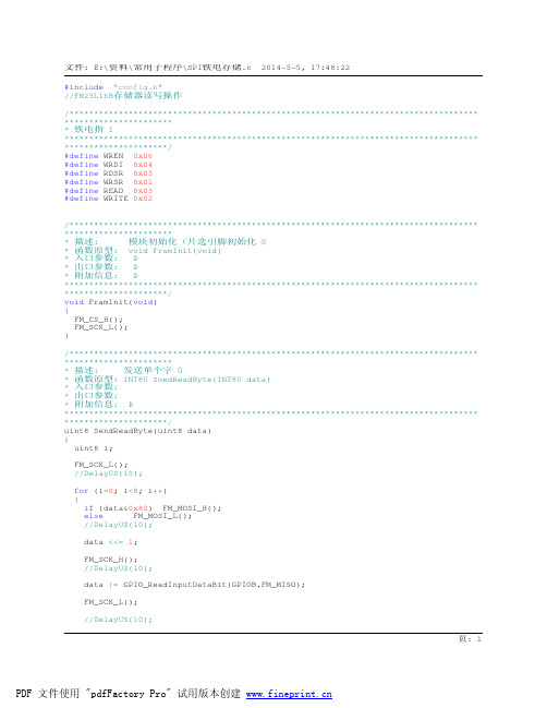
* 入口参数:
* 出口参数:
* 附加信息: Þ
************************************************************************************
*********************/
uint8 SendReadByte(uint8 data)
*********************/
void FMReadMemory(uint16 add, uint8 *dat, uint16 len)
{
uint16 i;
FM_CS_L();
SendReadByte(READ); SendReadByte((uint8)(add >> 8)); SendReadByte((uint8)(add)); for(i = 0; i < len; i++) {
**********************
* 描述:
往铁电里写数 Ý
* 函数原型: void FMWriteMemory(INT16U add, INT8U* dat, INT16U len)
* 入口参数:
* 出口参数:
* 附加信息: Þ
************************************************************************************
{
uint8 i;
FM_SCK_L(); //DelayUS(10);
for (i=0; i<8; i++)
{
if (data&0x80) FM_MOSI_H();
W-FM25说明书(中文)

—威索—手册安装使用说明书合格认证6004000002制造商: 麦克斯威索有限公司地址: Max-Weishaupt-StraßeD-88475Schwendi产品:燃烧管理器W-FM25上述产品符合下列指令的规定:GAD2009/142/ECPED97/23/ECLVD2006/95/ECEMC2004/108/EC产品标有如下信息:Schwendi,02.09.2014ppa.ppa.Dr.Schloen 研发部门经理Denkinger生产与质量管理经理1用户须知 (6)1.1用户指南 (6)1.1.1符号 (6)1.1.2目标客户群 (8)1.2担保与责任 (8)2安全 (10)2.1指定应用 (10)2.2有燃气味时 (10)2.3安全措施 (11)2.3.1正常操作 (11)2.3.2电气连接 (11)2.3.3供气 (12)2.4对设备结构的改动 (12)2.5噪声排放 (12)2.6废品处理 (13)3产品说明 (14)3.1输入与输出 (14)3.1.1燃气燃烧器 (14)3.1.2燃油燃烧器 (16)3.1.3双燃料燃烧器 (18)3.2技术数据 (20)3.2.1电气数据 (20)3.2.2环境条件 (20)3.2.3尺寸 (21)4操作 (22)4.1操作面板 (22)4.2显示屏 (25)4.2.1信息菜单 (27)4.2.2服务菜单 (33)4.2.3参数菜单 (37)4.2.4访问菜单 (44)4.3线性化 (46)5电气连接 (48)6调试 (49)6.1燃气燃烧器 (49)6.2带速度控制的燃气燃烧器 (55)6.3燃油燃烧器 (62)6.4双燃料燃烧器 (68)6.4.1调节气体侧 (68)6.4.2调节燃油侧 (74)7.故障排除 (80)7.1故障发生时的操作 (80)7.1.1显示屏关闭 (80)7.1.1显示屏闪烁 (80)7.1.3详细的故障代码 (81)7.2修复故障 (82)8零备件 (87)9技术文件 (89)9.1程序序列 (89)10关键词索引661用户须知本安装使用说明书构成设备的重要组成部分,必须始终在现场保存。
Flash ROM ST25P16中文资料
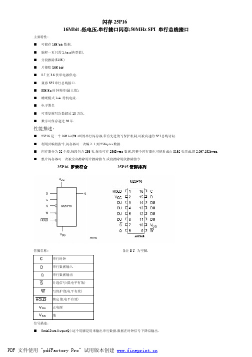
■ 闪存器可被外围带 SPI 的控制器驱动并工作在下面两种模式下: CPOL=0 , CPHA=0 CPOL=1 , CPHA=1 在这两种模式下,输入数据都是在时钟信号上升沿锁入闪存器,输出数据是利用时钟信号的下降沿输出. 这两种模式的区如图 6 所示,时钟极性是在总线控制器在标准模式下不传输数据的极性: ------- C remains at 0 for (CPOL=0,CPHA=0) ------- C remains at 0 for(CPOL=1,CPHA=0)
串行数据输入
串行数据输出
片选信号(低电平有效)
写保护(低电平有效)
锁定(低电平有效)
正电源
地
信号描述: ■ Serial Data Output(Q):这个用脚是用来输出串行数据.数据在时钟信号下降沿输出.
PDF 文件使用 "pdfFactory Pro" 试用版本创建
时: ◇ 上电重启 ◇ 写取消指令(WRDI)完成 ◇ 写状态寄存器指令(WRSR)完成 ◇ 页编程指令(PP)完成 ◇ 段擦除指令(SE)完成 ◇ 片擦除指令(BE)完成
■ 块保护位(BP2,BP1,BP0)可设置闪存器部分区域只能被读,不能写入,这就是软件保护模式(SPM) ■ 写保护信号(W)允许块保护位(BP2,BP1,BP0)和状太寄存器写保护位(SRWD)位被保护.这就是硬件保护模式(HPM). ■ 除低功耗之外,掉电模式提供了额外软件保护,此时所有的写入,编程,擦除指令都不被处理.
■ 如果锁定信号不是在时钟信为低电平时产生,锁定状态将在下一个时钟信号为低时生效.同样地如果取消锁定信号不是 在时钟信号为低时产生,锁定取消将在下一个时钟信号为低时生效.
■ 在锁定状态中,串行输出端(Q)为高阻抗,串行输入数据(D)和串行时钟信号都不被处理. ■ 通常,在整个锁定过程中都被处选中状态,即片选信号(S)为低.这是为了确保进入锁定状态的储存器内部逻辑数据不变. ■ 如果片选信号(S)在锁定过程中变为高电平,这将对闪存器内部逻辑的重新编排有影响.重启闪存器的通信,这必须使锁定信
FM25CL64中文
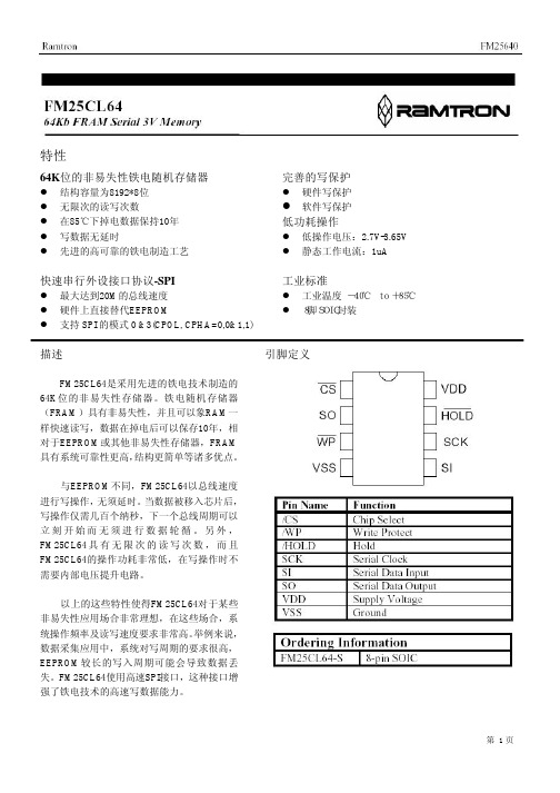
一些操作码是没有并发数据传输的命令,/CS信 号在一个操作完成后及一个新操作开始前必须无效, 在一个有效的芯片选择周期内,只能发出一个合法的 操作码。
第 3页
第 4页
数据传输 所有移进或移出FM25CL64的数据都是以8位为一
组,它们与时钟信号同步(SCK),同时以最高有效位 在前的方式传送(D7最先传送),串行数据在时钟的上 升沿移进,在时钟的下降沿移出
这种方案提供一种写保护的机制,它可以阻止任 何情况下的软件写操作,要达到这种效果必须将 BP1 和 BP0 设置为 1,WPEN 设置为 1,同时/WP 配置为 0。这是因为块保护位保护了内存的写入, 同时/WP 信号在硬件上禁止对块保护位的修改, (如果 WPEN 为设置为高),在这样的情况下, 硬件与内存写保护是相关的,下表总结了写保护 的情况。
WRSR-Write Status Register
WRSR 命令允许用户通过向状态寄存器写一个字 节来选
择特定的写保护状态。在发布一个WRSR 命令之前,/WP引脚必须为高电平或者无 效。必须注意,对于FM25CL64而言,/WP 仅仅禁止向状态寄存器的写入,而不是禁 止对内存的写入,在写入WRSR命令之 前,用户必须写WREN命令以置位写使 能。请注意,执行一个WRSR命令就是一 个写操作,完成后复位写使能寄存器。 RDSR 及 WRSR 的 总 线 时 序 在 下 图 中 描 述。
l 最大达到20M的总线速度 l 硬件上直接替代EEPROM l 支持 SPI 的模式 0 &3(CPOL, CPHA=0,0&1,1)
工业标准
l 工业温度 -40℃ to +85℃ l 8脚SOIC封装
描述
引脚定义
FM25CL64是采用先进的铁电技术制造的 64K位的非易失性存储器。铁电随机存储器 (FRAM)具有非易失性,并且可以象RAM一 样快速读写,数据在掉电后可以保存10年,相 对于EEPROM或其他非易失性存储器,FRAM 具有系统可靠性更高,结构更简单等诸多优点。
STTH25M06 高速恢复电源电路芯片说明书

STTH25M06B-TR STTH25M06FPDPAKTO220FPAC Features•Ultrafast recovery, soft recovery•Low power losses at high switching frequency operations•Low leakage current•High junction temperature•High overcurrent capability•ECOPACK2 compliantApplications•PFC•Boost diode•LLC clamping diodeDescriptionThe STTH25M06 is an ultrafast recovery power rectifier especially suited for boost or LLC clamping circuits working at high switching frequencies in heavy duty applications such as air conditioning equipment or telecom power supplies. Designed with the latest ST’s ultrafast technology, this 600 V 25 A diode in DPAK and TO-220FPAC has a robust behavior against electrostatic discharge and high overcurrent capability.600 V, 25 A ultrafast high voltage diodeSTTH25M06DatasheetSTTH25M06Characteristics 1CharacteristicsTable 1. Absolute ratings (limiting values at 25 °C, unless otherwise specified)Table 2. Thermal resistance parameterFor more information, please refer to the following application note :•AN5088 : Rectifiers thermal management, handling and mounting recommendationsTable 3. Static electrical characteristics1.Pulse test: t p = 5 ms, δ < 2%2.Pulse test: t p = 380 µs, δ < 2%To evaluate the conduction losses, use the following equation:P = 1.04 x I F(AV) + 0.0385 x I F2(RMS)For more information, please refer to the following application notes related to the power losses :•AN604: Calculation of conduction losses in a power rectifier•AN4058: Calculation of turn-off power losses generated by an ultrafast diodeSTTH25M06Characteristics Table 4. Dynamic electrical characteristicsSTTH25M06Characteristics (curves) 1.1Characteristics (curves)STTH25M06 Characteristics (curves)Figure 13. Relative variation of non-repetitive peak surgeforward current versus pulse duration (sinusoidalwaveform)1.01.52.02.53.0 3.54.00.11.010.0I FSM (t p ) / I FSM (10ms)t p (ms)Figure 14. Relative variation of non-repetitive peak surge forward current versus initial junction temperature(sinusoidal waveform)I FSM (T j ) / I FSM (25 °C)T j (°C)0.0 0.20.40.60.81.01.22550 75 100 125 150 175STTH25M06Characteristics (curves)2Package informationIn order to meet environmental requirements, ST offers these devices in different grades of ECOPACK packages,depending on their level of environmental compliance. ECOPACK specifications, grade definitions and product status are available at: . ECOPACK is an ST trademark.2.1DPAK package information•Epoxy meets UL 94,V0•Cooling method: by conduction (C)Figure 15. DPAK package outlineNote:This package drawing may slightly differ from the physical package. However, all the specified dimensions are guaranteed.STTH25M06Package informationSTTH25M06DPAK package information Table 5. DPAK package mechanical dataFigure 16. DPAK recommended footprint (dimensions in mm)The device must be positioned within0.05AB2.2TO-220FPAC package information•Epoxy meets UL 94,V0•Cooling method: by conduction (C)•Recommended torque value: 0.55 N·m•Maximum torque value: 0.70 N·mFigure 17.TO-220FPAC package outlineSTTH25M06TO-220FPAC package informationTO-220FPAC package information Table 6. TO-220FPAC package mechanical dataOrdering information 3Ordering informationTable 7. Ordering informationRevision historyTable 8. Document revision historyIMPORTANT NOTICE – PLEASE READ CAREFULLYSTMicroelectronics NV and its subsidiaries (“ST”) reserve the right to make changes, corrections, enhancements, modifications, and improvements to ST products and/or to this document at any time without notice. Purchasers should obtain the latest relevant information on ST products before placing orders. ST products are sold pursuant to ST’s terms and conditions of sale in place at the time of order acknowledgement.Purchasers are solely responsible for the choice, selection, and use of ST products and ST assumes no liability for application assistance or the design of Purchasers’ products.No license, express or implied, to any intellectual property right is granted by ST herein.Resale of ST products with provisions different from the information set forth herein shall void any warranty granted by ST for such product.ST and the ST logo are trademarks of ST. For additional information about ST trademarks, please refer to /trademarks. All other product or service names are the property of their respective owners.Information in this document supersedes and replaces information previously supplied in any prior versions of this document.© 2020 STMicroelectronics – All rights reservedSTTH25M06B-TR STTH25M06FP。
GD25LQ16_Rev1.5
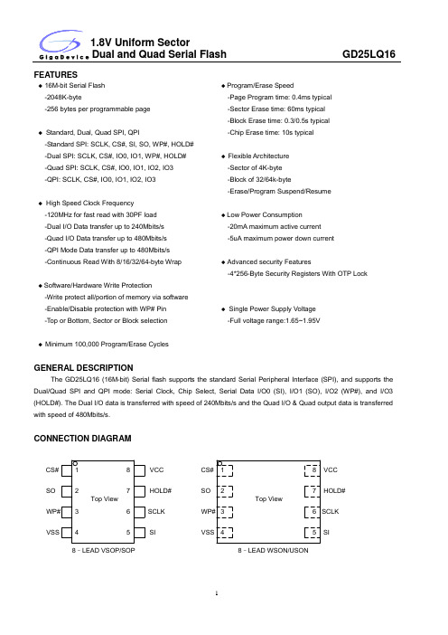
4
1.8V Uniform Sector Dual and Quad Serial Flash
GD25LQ16
BLOCK DIAGRAM
Write Control Logic Status Register High Voltage Generators Page Address Latch/Counter
WP#(IO2)
Write Protect Logic and Row Decode
HOLD#(IO3) SCLK CS# SI(IO0) SO(IO1)
3
1.8V Uniform Sector Dual and Quad Serial Flash
DEVICE OPERATION SPI Mode
Standard SPI
GD25LQ16
The GD25LQ16 features a serial peripheral interface on 4 signals bus: Serial Clock (SCLK), Chip Select (CS#), Serial Data Input (SI) and Serial Data Output (SO). Both SPI bus mode 0 and 3 are supported. Input data is latched on the rising edge of SCLK and data shifts out on the falling edge of SCLK.
1
1.8V Uniform Sector Dual and Quad Serial Flash
PIN DESCRIPTION
Pin Name CS# SO (IO1) WP# (IO2) VSS SI (IO0) SCLK HOLD# (IO3) VCC I/O I I/O I/O I I/O I/O Description Chip Select Input Data Output (Data Input Output 1) Write Protect Input (Data Input Output 2) Ground Data Input (Data Input Output 0) Serial Clock Input Hold Input (Data Input Output 3) Power Supply
XR16L2550资料
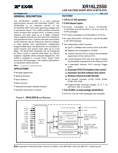
áçXR16L2550LOW VOLTAGE DUART WITH 16-BYTE FIFO SEPTEMBER 2003REV. 1.0.0GENERAL DESCRIPTIONThe XR16L25501 (L2550) is a dual universal asynchronous receiver and transmitter (UART). The XR16L2550 is an improved version of the ST16C2550 UART with lower operating voltages and 5 volt tolerant inputs. The L2550 provides enhanced UART functions with 16 byte FIFOs, a modem control interface and data rates up to 4 Mbps. Onboard status registers provide the user with error indications and operational status. System interrupts and modem control features may be tailored by external software to meet specific user requirements. Independent programmable baud rate generators are provided to select transmit and receive clock rates up to 3.125 Mbps. The Baud Rate Generator can be configured for either crystal or external clock input. An internal loopback capability allows onboard diagnostics. The L2550 is available in a 44-pin PLCC, 48-pin TQFP and 32-pin QFN packages. The L2550 is fabricated in an advanced CMOS process.N OTE: 1 Covered by U.S. Patent #5,649,122.APPLICATIONS•Portable Appliances•Medical Monitors•Base Stations•Micro Servers•T elecommunication Network Routers •Industrial Automation Controls FEATURES•2.25 to 5.5 Volt operation•5 Volt tolerant inputs•Pin-to-pin compatible to Exar’s ST16C2450, ST16C2550 and XR16L2750 in 44-PLCC and 48-TQFP packages•Pin-to-pin compatible to XR16C2850 in 44-PLCC •Pin alike XR16L2551, XR16L2751 and XR16C2850 in 48-TQFP package•T wo independent UART channelss Up to 3.125Mbps with external clock of 50 MHz s Register Set compatible to 16C550s16 byte T ransmit FIFO to reduce the bandwidth requirement of the external CPUs16 byte Receive FIFO with error tags to reduce the bandwidth requirement of the external CPUs 4 selectable Receive FIFO interrupt trigger levelss Automatic RTS/CTS hardware flow controls Automatic Xon/Xoff software flow controls Wireless infrared encoder/decoders Full Modem Interface (CTS#, RTS#, DSR#, DTR#, RI#, CD#)s Programmable character lengths (5, 6, 7, 8) with even, odd, or no parity•Tiny 32-QFN, no lead package (5x5x0.9mm)•44-PLCC and 48-TQFP packages also availableF IGURE 1. XR16L2550 B LOCK D IAGRAM元器件交易网Exar Corporation 48720 Kato Road, Fremont CA, 94538 • (510) 668-7000 • FAX (510) 668-7017 • XR16L2550áçLOW VOLTAGE DUART WITH 16-BYTE FIFO REV. 1.0.02F IGURE 2. P IN O UT A SSIGNMENTORDERING INFORMATIONP ART N UMBER P ACKAGE O PERATING T EMPERATURE R ANGED EVICE S TATUSXR16L2550IL 32-Lead QFN -40°C to +85°C Active XR16L2550IJ 44-Lead PLCC -40°C to +85°C Active XR16L2550IM48-Lead TQFP-40°C to +85°CActiveáçXR16L2550REV. 1.0.0LOW VOLTAGE DUART WITH 16-BYTE FIFO3PIN DESCRIPTIONSPin DescriptionN AME32-QFN P IN #44-PLCC P IN #48-TQFP P IN #T YPED ESCRIPTIONDATA BUS INTERFACEA2A1A0181920293031262728IAddress data lines [2:0]. These 3 address lines select one of the internal registers in UART channel A/B during a data bus transaction.D7D6D5D4D3D2D1D021323130292827987654323214847464544IOData bus lines [7:0] (bidirectional).IOR#142419IInput/Output Read Strobe (active low). The falling edge instigates an internal read cycle and retrieves the data byte from an internal register pointed to by the address lines [A2:A0]. The data byte is placed on the data bus to allow the host processor to read it on the rising edge. IOW#122015IInput/Output Write Strobe (active low). The falling edge instigates an internal write cycle and the rising edge transfers the data byte on the data bus to an internal reg-ister pointed by the address lines.CSA#71610I UART channel A select (active low) to enable UART chan-nel A in the device for data bus operation.CSB#81711I UART channel B select (active low) to enable UART chan-nel B in the device for data bus operation.INT A223330OUART channel A Interrupt output. The output state is defined by the user and through the software setting of MCR[3]. INT A is set to the active mode (active high) and OP2A# output to a logic 0 when MCR[3] is set to a logic 1. INT A is set to the three state mode and OP2A# to a logic 1 when MCR[3] is set to a logic 0 (Default). INTB 213229OUART channel B Interrupt output. The output state is defined by the user and through the software setting of MCR[3]. INTB is set to the active mode and OP2B# out-put to a logic 0 when MCR[3] is set to a logic 1. INTB is set to the three state mode and OP2B# to a logic 1 when MCR[3] is set to a logic 0 (Default).TXRDY A#-143OUART channel A T ransmitter Ready (active low). The output provides the TX FIFO/THR status for transmit channel A. If it is not used, leave it unconnected.RXRDY A#-3431OUART channel A Receiver Ready (active low). This output provides the RX FIFO/RHR status for receive channel A. If it is not used, leave it unconnected.XR16L2550áçLOW VOLTAGE DUART WITH 16-BYTE FIFO REV. 1.0.04TXRDYB#-126OUART channel B T ransmitter Ready (active low). The out-put provides the TX FIFO/THR status for transmit channel B. If it is not used, leave it unconnected.RXRDYB#-2318OUART channel B Receiver Ready (active low). This output provides the RX FIFO/RHR status for receive channel B. If it is not used, leave it unconnected.MODEM OR SERIAL I/O INTERFACETXA 5137O UART channel A T ransmit Data. If it is not used, leave it unconnected.RXA4115IUART channel A Receive Data. Normal receive data input must idle at logic 1 condition. If it is not used, tie it to VCC or pull it high via a 100k ohm resistor.RTSA#233633OUART channel A Request-to-Send (active low) or general purpose output. This output must be asserted prior to using auto RTS flow control, see EFR[6], MCR[1] and IER[6]. If it is not used, leave it unconnected.CTSA#254038IUART channel A Clear-to-Send (active low) or general purpose input. It can be used for auto CTS flow control, see EFR[7] and IER[7]. This input should be connected to VCC when not used.DTRA#-3734OUART channel A Data-T erminal-Ready (active low) or general purpose output. If it is not used, leave it uncon-nected.DSRA#-4139IUART channel A Data-Set-Ready (active low) or general purpose input. This input should be connected to VCC when not used. This input has no effect on the UART .CDA#-4240IUART channel A Carrier-Detect (active low) or general purpose input. This input should be connected to VCC when not used. This input has no effect on the UART .RIA#-4341IUART channel A Ring-Indicator (active low) or general purpose input. This input should be connected to VCC when not used. This input has no effect on the UART .OP2A#-3532OOutput Port 2 Channel A - The output state is defined by the user and through the software setting of MCR[3]. INT A is set to the active mode and OP2A# output to a logic 0 when MCR[3] is set to a logic 1. INT A is set to the three state mode and OP2A# to a logic 1 when MCR[3] is set to a logic 0. This output should not be used as a gen-eral output else it will disturb the INT A output functionality. If it is not used at all, leave it unconnected.TXB 6148O UART channel B T ransmit Data. If it is not used, leave it unconnected.RXB3104IUART channel B Receive Data. Normal receive data input must idle at logic 1 condition. If it is not used, tie it to VCC or pull it high via a 100k ohm resistor.Pin DescriptionN AME 32-QFN P IN #44-PLCC P IN #48-TQFP P IN #T YPE D ESCRIPTIONáçXR16L2550REV. 1.0.0LOW VOLTAGE DUART WITH 16-BYTE FIFO5Pin type: I=Input, O=Output, IO= Input/output, OD=Output Open Drain.1.0PRODUCT DESCRIPTIONThe XR16L2550 (L2550) provides serial asynchronous receive data synchronization, parallel-to-serial and serial-to-parallel data conversions for both the transmitter and receiver sections. These functions areRTSB#152722OUART channel B Request-to-Send (active low) or general purpose output. This output must be asserted prior to using auto RTS flow control, see EFR[6], MCR[1] and IER[6]. If it is not used, leave it unconnected.CTSB#162823IUART channel B Clear-to-Send (active low) or general purpose input. It can be used for auto CTS flow control, see EFR[7] and IER[7]. This input should be connected to VCC when not used.DTRB#-3835OUART channel B Data-T erminal-Ready (active low) or general purpose output. If it is not used, leave it uncon-nected.DSRB#-2520IUART channel B Data-Set-Ready (active low) or general purpose input. This input should be connected to VCC when not used. This input has no effect on the UART .CDB#-2116IUART channel B Carrier-Detect (active low) or general purpose input. This input should be connected to VCC when not used. This input has no effect on the UART .RIB#-2621IUART channel B Ring-Indicator (active low) or general purpose input. This input should be connected to VCC when not used. This input has no effect on the UART .OP2B#-159OOutput Port 2 Channel B - The output state is defined by the user and through the software setting of MCR[3]. INTB is set to the active mode and OP2B# output to a logic 0 when MCR[3] is set to a logic 1. INTB is set to the three state mode and OP2B# to a logic 1 when MCR[3] is set to a logic 0. This output should not be used as a gen-eral output else it will disturb the INTB output functionality. If it is not used, leave it unconnected.ANCILLARY SIGNALS XT AL1101813I Crystal or external clock input. XT AL2111914O Crystal or buffered clock output.RESET243936IReset (active high) - A longer than 40 ns logic 1 pulse on this pin will reset the internal registers and all outputs. The UART transmitter output will be held at logic 1, the receiver input will be ignored and outputs are reset during reset period.VCC 264442Pwr 2.25V to 5.5V power supply. All inputs are 5V tolerant.GND 132217PwrPower supply common, ground.N.C.9, 17-12, 24, 25,37No Connection. These pins are open, but typically , should be connected to GND for good design practice.Pin DescriptionN AME 32-QFN P IN #44-PLCC P IN #48-TQFP P IN #T YPE D ESCRIPTIONXR16L2550áçLOW VOLTAGE DUART WITH 16-BYTE FIFOREV. 1.0.06necessary for converting the serial data stream into parallel data that is required with digital data systems.Synchronization for the serial data stream is accomplished by adding start and stop bits to the transmit data to form a data character (character orientated protocol). Data integrity is ensured by attaching a parity bit to the data character. The parity bit is checked by the receiver for any transmission bit errors. The electronic circuitry to provide all these functions is fairly complex especially when manufactured on a single integrated silicon chip.The L2550 represents such an integration with greatly enhanced features. The L2550 is fabricated with an advanced CMOS process.Transmit and Receive FIFOs (16 Bytes each)The L2550 is an upward solution that provides a dual UART capability with 16 bytes of transmit and receive FIFO memory, instead of none in the 16C2450. The L2550 is designed to work with high speed modems and shared network environments, that require fast data processing time. Increased performance is realized in the L2550 by the transmit and receive FIFO’s. This allows the external processor to handle more networking tasks within a given time. For example, the ST16C2450 without a receive FIFO, will require unloading of the RHR in 93 microseconds (This example uses a character length of 11 bits, including start/stop bits at 115.2 Kbps). This means the external CPU will have to service the receive FIFO less than every 100 microseconds. However with the 16 byte FIFO in the L2550, the data buffer will not require unloading/loading for 1.53 ms. This increases the service interval giving the external CPU additional time for other applications and reducing the overall UART interrupt servicing time. In addition, the 4 selectable receive FIFO trigger interrupt levels is uniquely provided for maximum data throughput performance especially when operating in a multi-channel environment. The FIFO memory greatly reduces the bandwidth requirement of the external controlling CPU, increases performance, and reduces power consumption.Data RateThe L2550 is capable of operation up to 3.125 Mbps with a 50 MHz clock. With a crystal or external clock input of 14.7456 MHz the user can select data rates up to 921.6 Kbps.Enhanced FeaturesThe XR16L2550 integrates the functions of 2 enhanced 16C550 Universal Asynchronous Receiver and T ransmitter (UART). Each UART is independently controlled having its own set of device configuration registers. The configuration registers set is 16550 UART compatible for control, status and data transfer.Additionally, each UART channel has automatic RTS/CTS hardware flow control, automatic Xon/Xoff and special character software flow control, infrared encoder and decoder (IrDA ver 1.0), programmable baud rate generator with a prescaler of divide by 1 or 4, and data rate up to 4 Mbps at 5V .The rich feature set of the L2550 is available through internal registers. Selectable receive FIFO trigger levels,selectable TX and RX baud rates, and modem interface controls are all standard features. Following a power on reset or an external reset, the L2550 is functionally and software compatible with the previous generation ST16C2450 and ST16C2550.áçXR16L2550REV. 1.0.0LOW VOLTAGE DUART WITH 16-BYTE FIFO72.0FUNCTIONAL DESCRIPTIONS 2.1CPU InterfaceThe CPU interface is 8 data bits wide with 3 address lines and control signals to execute data bus read and write transactions. The L2550 data interface supports the Intel compatible types of CPUs and it is compatible to the industry standard 16C550 UART . No clock (oscillator nor external clock) is required to operate a data bus transaction. Each bus cycle is asynchronous using CS#, IOR# and IOW# signals. Both UART channels share the same data bus for host operations. The data bus interconnections are shown in Figure 3.2.25-Volt Tolerant InputsThe L2550 can accept up to 5V inputs even when operating at 3.3V or 2.5V . But note that if the L2550 is operating at 2.5V , its V OH may not be high enough to meet the requirements of the V IH of a CPU or a serial transceiver that is operating at 5V . 2.3Device ResetThe RESET input resets the internal registers and the serial interface outputs in both channels to their default state (see T able 13). An active high pulse of at least 40 ns duration will be required to activate the reset function in the device.2.4Channel A and B SelectionThe UART provides the user with the capability to bi-directionally transfer information between an external CPU and an external serial communication device. A logic 0 on chip select pins, CSA# or CSB#, allows the user to select UART channel A or B to configure, send transmit data and/or unload receive data to/from the UART .Selecting both UARTs can be useful during power up initialization to write to the same internal registers, but do not attempt to read from both uarts simultaneously. Individual channel select functions are shown in T able 1.F IGURE 3. XR16L2550 D ATA B US I NTERCONNECTIONST ABLE 1: C HANNEL A AND B S ELECTCSA#CSB#F UNCTION 11UART de-selected 01Channel A selectedXR16L2550áçLOW VOLTAGE DUART WITH 16-BYTE FIFOREV. 1.0.082.5Channel A and B Internal RegistersEach UART channel in the L2550 has a standard register set for controlling, monitoring and data loading and unloading. The configuration register set is compatible to those already available in the standard single 16C550. These registers function as data holding registers (THR/RHR), interrupt status and control registers (ISR/IER), a FIFO control register (FCR), receive line status and control registers (LSR/LCR), modem status and control registers (MSR/MCR), programmable data rate (clock) divisor registers (DLL/DLM), and a user accessible scratch pad register (SPR). 2.6DMA ModeThe device does not support direct memory access. The DMA Mode (a legacy term) in this document doesn’t mean “direct memory access” but refers to data block transfer operation. The DMA mode affects the state of the RXRDY# A/B and TXRDY# A/B output pins. The transmit and receive FIFO trigger levels provide additional flexibility to the user for block mode operation. The LSR bits 5-6 provide an indication when the transmitter is empty or has an empty location(s) for more data. The user can optionally operate the transmit and receive FIFO in the DMA mode (FCR bit-3=1). When the transmit and receive FIFO are enabled and the DMA mode is disabled (FCR bit-3 = 0), the L2550 is placed in single-character mode for data transmit or receive operation.When DMA mode is enabled (FCR bit-3 = 1), the user takes advantage of block mode operation by loading or unloading the FIFO in a block sequence determined by the programmed trigger level. The following table show their behavior. Also see Figure 18 through Figure 23.2.7INTA and INTB OutputsThe INT A and INTB interrupt output changes according to the operating mode and enhanced features setup.T able 3 and T able 4 summarize the operating behavior for the transmitter and receiver. Also see Figure 18through Figure 23.10Channel B selected 0Channel A and B selectedT ABLE 2: TXRDY# AND RXRDY# O UTPUTS IN FIFO AND DMA M ODEP INSFCR BIT -0=0(FIFO D ISABLED )FCR B IT -0=1 (FIFO E NABLED )FCR Bit-3 = 0(DMA Mode Disabled)FCR Bit-3 = 1(DMA Mode Enabled)RXRDY# A/B0 = 1 byte. 1 = no data.0 = at least 1 byte in FIFO 1 = FIFO empty.1 to 0 transition when FIFO reaches the trigger level, or time-out occurs.0 to 1 transition when FIFO empties. TXRDY# A/B0 = THR empty .1 = byte in THR.0 = FIFO empty.1 = at least 1 byte in FIFO.0 = FIFO has at least 1 empty location.1 = FIFO is full.T ABLE 3: INTA AND INTB P INS O PERATION FOR T RANSMITTERFCR B IT -0 = 0 (FIFO D ISABLED )FCR B IT -0 = 1 (FIFO E NABLED )INT A/B Pin0 = a byte in THR 1 = THR empty0 = at least 1 byte in FIFO 1 = FIFO emptyT ABLE 1: C HANNEL A AND B S ELECTCSA#CSB#F UNCTIONáçXR16L2550REV. 1.0.0LOW VOLTAGE DUART WITH 16-BYTE FIFO92.8Crystal Oscillator or External Clock InputThe L2550 includes an on-chip oscillator (XT AL1 and XT AL2) to produce a clock for both UART sections in the device. The CPU data bus does not require this clock for bus operation. The crystal oscillator provides a system clock to the Baud Rate Generators (BRG) section found in each of the UART . XT AL1 is the input to the oscillator or external clock buffer input with XT AL2 pin being the output. For programming details, see “Programmable Baud Rate Generator.”The on-chip oscillator is designed to use an industry standard microprocessor crystal (parallel resonant,fundamental frequency with 10-22 pF capacitance load, ESR of 20-120 ohms and 100 ppm frequency tolerance) connected externally between the XT AL1 and XT AL2 pins (see Figure 4), with an external 500 k Ω to 1 M Ω resistor across it. Alternatively, an external clock can be connected to the XT AL1 pin to clock the internal baud rate generator for standard or custom rates. T ypical oscillator connections are shown in Figure 4. For further reading on oscillator circuit please see application note DAN108 on EXAR’s web site.T ABLE 4: INTA AND INTB P IN O PERATION F OR R ECEIVERFCR B IT -0 = 0 (FIFO D ISABLED )FCR B IT -0 = 1 (FIFO E NABLED )INT A/B Pin0 = no data 1 = 1 byte0 = FIFO below trigger level 1 = FIFO above trigger levelF IGURE 4. T YPICAL OSCILLATOR CONNECTIONSXR16L2550áçLOW VOLTAGE DUART WITH 16-BYTE FIFO REV. 1.0.0102.9Programmable Baud Rate GeneratorA single baud rate generator is provided for the transmitter and receiver, allowing independent TX/RX channel control. The programmable Baud Rate Generator is capable of operating with a crystal frequency of up to 24MHz. However, with an external clock input on XT AL1 pin and a 2K ohms pull-up resistor on XT AL2 pin (as shown in Figure 5) it can extend its operation up to 64 MHz (4Mbps serial data rate) at room temperature and 5.0V .T o obtain maximum data rate, it is necessary to use full rail swing on the clock input. See external clock operating frequency over power supply voltage chart in Figure 6.F IGURE 5. E XTERNAL C LOCK C ONNECTION FOR E XTENDED D ATA R ATEF IGURE 6. O PERATING F REQUENCY C HART . R EQUIRES A 2K OHMS PULL -UP RESISTOR ON XTAL2 PIN TO INCREASE OPERATING SPEEDThe L2550 divides the basic external clock by 16. The basic 16X clock provides table rates to support standard and custom applications using the same system design. The Baud Rate Generator divides the input 16X clock by any divisor from 1 to 216 -1. The rate table is configured via the DLL and DLM internal register functions.Customized Baud Rates can be achieved by selecting the proper divisor values for the MSB and LSB sections of baud rate generator.T able 5 shows the standard data rates available with a 14.7456 MHz crystal or external clock at 16X sampling rate. When using a non-standard frequency crystal or external clock, the divisor value can be calculated for DLL/DLM with the following equation.2.10TransmitterThe transmitter section comprises of an 8-bit T ransmit Shift Register (TSR) and 16 bytes of FIFO which includes a byte-wide T ransmit Holding Register (THR). TSR shifts out every data bit with the 16X internal clock.A bit time is 16 clock periods. The transmitter sends the start-bit followed by the number of data bits, inserts the proper parity-bit if enabled, and adds the stop-bit(s). The status of the FIFO and TSR are reported in the Line Status Register (LSR bit-5 and bit-6). 2.10.1Transmit Holding Register (THR) - Write OnlyThe transmit holding register is an 8-bit register providing a data interface to the host processor. The host writes transmit data byte to the THR to be converted into a serial data stream including start-bit, data bits,parity-bit and stop-bit(s). The least-significant-bit (Bit-0) becomes first data bit to go out. The THR is the input register to the transmit FIFO of 16 bytes when FIFO operation is enabled by FCR bit-0. Every time a write operation is made to the THR, the FIFO data pointer is automatically bumped to the next sequential data location. 2.10.2Transmitter Operation in non-FIFO ModeThe host loads transmit data to THR one character at a time. The THR empty flag (LSR bit-5) is set when the data byte is transferred to TSR. THR flag can generate a transmit empty interrupt (ISR bit-1) when it is enabled by IER bit-1. The TSR flag (LSR bit-6) is set when TSR becomes completely empty.divisor (decimal) = (XT AL1 clock frequency) / (serial data rate x 16)T ABLE 5: T YPICAL DATA RATES WITH A 14.7456 MH Z CRYSTAL OR EXTERNAL CLOCKO UTPUT Data Rate MCR Bit-7=0D IVISOR FOR 16x Clock (Decimal)D IVISOR FOR 16x Clock (HEX)DLM P ROGRAM V ALUE (HEX)DLL P ROGRAM V ALUE (HEX)D ATA R ATE E RROR (%)400230490009000240038418001 8004800192C000 C009600966000 60019.2k 483000 30038.4k 241800 18076.8k 120C 00 0C 0153.6k 60600 060230.4k 40400 040460.8k 20200 020921.6k1010001LOW VOLTAGE DUART WITH 16-BYTE FIFO REV. 1.0.0F IGURE 7. T RANSMITTER O PERATION IN NON-FIFO M ODE2.10.3Transmitter Operation in FIFO ModeThe host may fill the transmit FIFO with up to 16 bytes of transmit data. The THR empty flag (LSR bit-5) is set whenever the FIFO is empty. The THR empty flag can generate a transmit empty interrupt (ISR bit-1) when the transmit empty interrupt is enabled by IER bit-1. The TSR flag (LSR bit-6) is set when the FIFO and the TSR become empty.F IGURE 8. T RANSMITTER O PERATION IN FIFO AND F LOW C ONTROL M ODE2.11ReceiverThe receiver section contains an 8-bit Receive Shift Register (RSR) and 16 bytes of FIFO which includes a byte-wide Receive Holding Register (RHR). The RSR uses the 16X for timing. It verifies and validates every bit on the incoming character in the middle of each data bit. On the falling edge of a start or false start bit, an internal receiver counter starts counting at the 16X. After 8 clocks the start bit period should be at the center of the start bit. At this time the start bit is sampled and if it is still a logic 0 it is validated. Evaluating the start bit in this manner prevents the receiver from assembling a false character. The rest of the data bits and stop bits are sampled and validated in this same manner to prevent false framing. If there were any error(s), they are reported in the LSR register bits 2-4. Upon unloading the receive data byte from RHR, the receive FIFO pointer is bumped and the error tags are immediately updated to reflect the status of the data byte in RHR register. RHR can generate a receive data ready interrupt upon receiving a character or delay until it reaches the FIFO trigger level. Furthermore, data delivery to the host is guaranteed by a receive data ready time-out interruptwhen data is not received for 4 word lengths as defined by LCR[1:0] plus 12 bits time. This is equivalent to 3.7-4.6 character times. The RHR interrupt is enabled by IER bit-0.2.11.1Receive Holding Register (RHR) - Read-OnlyThe Receive Holding Register is an 8-bit register that holds a receive data byte from the Receive Shift Register. It provides the receive data interface to the host processor. The RHR register is part of the receive FIFO of 16 bytes by 11-bits wide, the 3 extra bits are for the 3 error tags to be reported in LSR register. When the FIFO is enabled by FCR bit-0, the RHR contains the first data character received by the FIFO. After the RHR is read, the next character byte is loaded into the RHR and the errors associated with the current data byte are immediately updated in the LSR bits 2-4.F IGURE 9. R ECEIVER O PERATION IN NON-FIFO M ODEF IGURE 10. R ECEIVER O PERATION IN FIFO AND A UTO RTS F LOW C ONTROL M ODELOW VOLTAGE DUART WITH 16-BYTE FIFO REV. 1.0.0 2.12Auto RTS (Hardware) Flow ControlAutomatic RTS hardware flow control is used to prevent data overrun to the local receiver FIFO. The RTS# output is used to request remote unit to suspend/resume data transmission. The auto RTS flow control features is enabled to fit specific application requirement (see Figure11):- Enable auto RTS flow control using EFR bit-6.- The auto RTS function must be started by asserting RTS# output pin (MCR bit-1 to logic 1 after it is enabled). - Enable RTS interrupt through IER bit-6 (after setting EFR bit-4). The UART issues an interrupt when the RTS# pin makes a transition from low to high: ISR bit-5 will be set to logic 1.2.13 Auto CTS Flow ControlAutomatic CTS flow control is used to prevent data overrun to the remote receiver FIFO. The CTS# input is monitored to suspend/restart the local transmitter. The auto CTS flow control feature is selected to fit specific application requirement (see Figure11):- Enable auto CTS flow control using EFR bit-7.- Enable CTS interrupt through IER bit-7 (after setting EFR bit-4). The UART issues an interrupt when the CTS# pin is de-asserted (logic 1): ISR bit-5 will be set to 1, and UART will suspend transmission as soon as the stop bit of the character in process is shifted out. T ransmission is resumed after the CTS# input is re-asserted (logic 0), indicating more data may be sent.。
广播电子Econo-Control 16 经济版控制器说明书
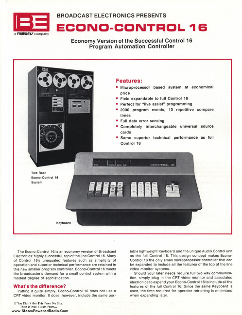
times • Full data error sensing • Completely interchangeable universal source
cards • Same superior technical performance as full
Control 16
Keyboard
The Econo-Control 16 is an economy version of Broadcast Electronics' highly successful, top of the line Control 16. Many of Control 16's unequaled features such as simplicity of operation and superior technical performance are retained in this new smaller program controller. Econo-Control 16 meets the broadcaster's demand for a small control system with a modest degree of sophistication.
- 1、下载文档前请自行甄别文档内容的完整性,平台不提供额外的编辑、内容补充、找答案等附加服务。
- 2、"仅部分预览"的文档,不可在线预览部分如存在完整性等问题,可反馈申请退款(可完整预览的文档不适用该条件!)。
- 3、如文档侵犯您的权益,请联系客服反馈,我们会尽快为您处理(人工客服工作时间:9:00-18:30)。
This product conforms to specifications per the terms of the Ramtron Ramtron International Corporationstandard warranty. The product has completed Ramtron’s internal1850 Ramtron Drive, Colorado Springs, CO 80921FM25L1616Kb FRAM Serial 3V MemoryFeatures16K bit Ferroelectric Nonvolatile RAM • Organized as 2,048 x 8 bits • Unlimited Read/Write Cycles • 45 Year Data Retention • NoDelay™ Writes• Advanced High-Reliability Ferroelectric ProcessVery Fast Serial Peripheral Interface - SPI • Up to 18 MHz Frequency• Direct Hardware Replacement for EEPROM • SPI Mode 0 & 3 (CPOL, CPHA=0,0 & 1,1)Sophisticated Write Protection Scheme • Hardware Protection • Software ProtectionLow Power Consumption• Low Voltage Operation 2.7-3.6V • 1 µA Standby CurrentIndustry Standard Configuration• Industrial Temperature -40°C to +85°C • “Green”/RoHS 8-pin SOIC Package • “Green”/RoHS 8-pin TDFN Package • TDFN Footprint Conforms to TSSOP-8DescriptionThe FM25L16 is a 16-kilobit nonvolatile memory employing an advanced ferroelectric process. A ferroelectric random access memory or FRAM is nonvolatile and performs reads and writes like a RAM. It provides reliable data retention for 45 years while eliminating the complexities, overhead, and system level reliability problems caused by EEPROM and other nonvolatile memories.Unlike serial EEPROMs, the FM25L16 performs write operations at bus speed. No write delays are incurred. Data is written to the memory array immediately after each byte has been transferred to the device. The next bus cycle may commence without the need for data polling. The product offers virtually unlimited write endurance, orders of magnitude more endurance than EEPROM. FRAM also exhibits much lower power during writes than EEPROM.These capabilities make the FM25L16 ideal for nonvolatile memory applications requiring frequent or rapid writes. Examples range from data collection, where the number of write cycles may be critical, to demanding industrial controls where the long write time of EEPROM can cause data loss.The FM25L16 provides substantial benefits to users of serial EEPROM as a hardware drop-in replacement. The FM25L16 uses the high-speed SPI bus, which enhances the high-speed write capability of FRAM technology. Device specifications are guaranteed over an industrial temperature range of -40°C to +85°C.Pin ConfigurationPin Name Function/CS Chip Select /WP Write Protect /HOLD Hold SCK Serial Clock SI Serial Data Input SO Serial Data Output VDD Supply Voltage VSS GroundOrdering InformationFM25L16-G “Green”/RoHS 8-pin SOIC FM25L16-DG “Green”/RoHS 8-pin TDFN/CS SO /WP VSSVDD /HOLD SCK SIOverviewThe FM25L16 is a serial FRAM memory. The memory array is logically organized as 2,048 x 8 and is accessed using an industry standard Serial Peripheral Interface or SPI bus. Functional operation of the FRAM is similar to serial EEPROMs. The major difference between the FM25L16 and a serial EEPROM with the same pinout is the FRAM’s superior write performance.Memory ArchitectureWhen accessing the FM25L16, the user addresses 2,048 locations of 8 data bits each. These data bits are shifted serially. The addresses are accessed using the SPI protocol, which includes a chip select (to permit multiple devices on the bus), an op-code, and a two-byte address. The upper 5 bits of the address range are ‘don’t care’ values. The complete address of 11-bits specifies each byte address uniquely.Most functions of the FM25L16 either are controlled by the SPI interface or are handled automatically by on-board circuitry. The access time for memory operation is essentially zero, beyond the time needed for the serial protocol. That is, the memory is read or written at the speed of the SPI bus. Unlike an EEPROM, it is not necessary to poll the device for a ready condition since writes occur at bus speed. So, by the time a new bus transaction can be shifted into the device, a write operation will be complete. This is explained in more detail in the interface section. Users expect several obvious system benefits from the FM25L16 due to its fast write cycle and high endurance as compared with EEPROM. In addition there are less obvious benefits as well. For example in a high noise environment, the fast-write operation is less susceptible to corruption than an EEPROM since it is completed quickly. By contrast, an EEPROM requiring milliseconds to write is vulnerable to noise during much of the cycle.Note that the FM25L16 contains no power management circuits other than a simple internal power-on reset. It is the user’s responsibility to ensure that V DD is within datasheet tolerances to prevent incorrect operation. It is recommended that the part is not powered down with chip select active.Serial Peripheral Interface – SPI BusThe FM25L16 employs a Serial Peripheral Interface (SPI) bus. It is specified to operate at speeds up to 18 MHz. This high-speed serial bus provides high performance serial communication to a host microcontroller. Many common microcontrollers have hardware SPI ports allowing a direct interface. It is quite simple to emulate the port using ordinary port pins for microcontrollers that do not. The FM25L16 operates in SPI Mode 0 and 3.The SPI interface uses a total of four pins: clock, data-in, data-out, and chip select. A typical system configuration uses one or more FM25L16 devices with a microcontroller that has a dedicated SPI port, as Figure 2 illustrates. Note that the clock, data-in, and data-out pins are common among all devices. The Chip Select and Hold pins must be driven separately for each FM25L16 device.For a microcontroller that has no dedicated SPI bus, a general purpose port may be used. To reduce hardware resources on the controller, it is possible to connect the two data pins (SI, SO) together and tie off (high) the Hold pin. Figure 3 shows a configuration that uses only three pins.Protocol OverviewThe SPI interface is a synchronous serial interface using clock and data pins. It is intended to support multiple devices on the bus. Each device is activated using a chip select. Once chip select is activated by the bus master, the FM25L16 will begin monitoring the clock and data lines. The relationship between the falling edge of /CS, the clock and data is dictated by the SPI mode. The device will make a determination of the SPI mode on the falling edge of each chip select. While there are four such modes, the FM25L16 supports Modes 0 and 3. Figure 4 shows the required signal relationships for Modes 0 and 3. For both modes, data is clocked into the FM25L16 on the rising edge of SCK and data is expected on the first rising edge after /CS goes active. If the clock begins from a high state, it will fall prior to beginning data transfer in order to create the first rising edge. The SPI protocol is controlled by op-codes. These op-codes specify the commands to the device. After /CS is activated the first byte transferred from the bus master is the op-code. Following the op-code, any addresses and data are then transferred. Note that the WREN and WRDI op-codes are commands with no subsequent data transfer.Important: The /CS must go inactive (high) after an operation is complete and before a new op-code can be issued. There is one valid op-code only per active chip select.。
