SZ65B2中文资料
mt6582中文规格书(部分)
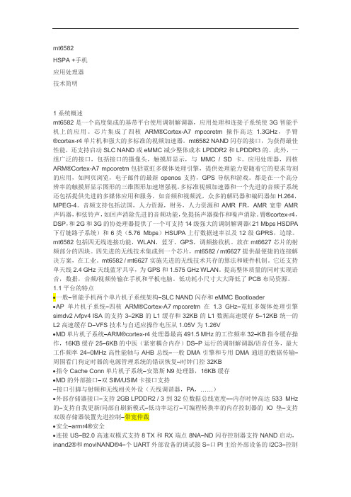
mt6582HSPA +手机应用处理器技术简明1系统概述mt6582是一个高度集成的基带平台使用调制解调器,应用处理和连接子系统使3G智能手机上的应用。
芯片集成了四核ARM®Cortex-A7 mpcoretm操作高达 1.3GHz,手臂®cortex-r4单片机和强大的多标准的视频加速器。
mt6582 NAND闪存的接口,为获得最佳性能,还支持启动SLC NAND或eMMC减少整体成本LPDDR2和LPDDR3的。
此外,一组广泛的接口,包括接口的摄像头,触摸屏显示,与MMC / SD卡。
应用处理器,四核ARM®Cortex-A7 mpcoretm包括霓虹多媒体处理引擎,提供处理能力要随着它的要求苛刻的应用,如网页浏览,电子邮件的最新openos支持,GPS导航和游戏。
都是在一个高分辨率的触摸屏显示图形的三维图形加速增强视。
多标准视频加速器和一个先进的音频子系统还包括提供先进的多媒体应用和服务,如音频和视频流,众多的解码器和编码器如H.264,MPEG-4。
音频支持包括法国,人力资源,财务,人力资源和AMR FR,AMR宽带AMR 声码器,和弦铃声,如回声消除先进的音频功能,免提扬声器操作和噪声消除。
臂®cortex-r4,DSP,和2G和3G的协处理器提供了一个可支持14级强大的调制解调器(21 Mbps HSDPA 下行链路子系统)和6类(5.76 Mbps)HSUPA上行数据速率以及12级GPRS,边缘。
mt6582包括四无线连接功能,WLAN,蓝牙,GPS,调频接收机。
放在mt6627芯片的射频部分的四块。
四先进的无线技术集成到一个芯片,mt6582 / mt6627提供最便捷的连接解决方案,在工业。
mt6582 / mt6627实施先进的无线技术共存的算法和硬件机制。
它还支持单天线2.4 GHz天线蓝牙共享,为GPS和1.575 GHz WLAN。
2SK3562中文资料
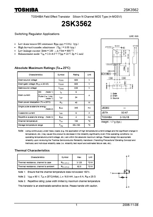
Channel temperature
Storage temperature range
VDSS VDGR VGSS
ID
IDP
PD
EAS
IAR EAR Tch Tstg
600
V
600
V
±30
V
6
A 24
40
W
345
mJ
6
A
4
mJ
150
°C
-55~150
°C
1: Gate 2: Drain 3: Source
5
Tc = 25°C
PULSE TEST
3
1
0.5 10
0.3
5
3
1
VGS = 0, −1 V
0.1
0
−0.2 −0.4 −0.6 −0.8
−1
−1.2
DRAIN-SOURCE VOLTAGE VDS (V)
CAPACITANCE C (pF)
10000 1000
CAPACITANCE – VDS
Ciss
1 VDS = 10 V ID = 1 mA
PULSE TEST
0
−80
−40
0
40
80
120
160
CASE TEMPERATURE Tc (°C)
PD – Tc
50
40 30
20
10
0
0
40
80
120
160
200
CASE TEMPERATURE Tc (°C)
DRAIN-SOURCE VOLTAGE VDS (V)
Thermal Characteristics
Drehgeber_WDG58B中文翻译

每圈脉冲数
PPR:
2, 10, 15, 20, 24, 25, 30, 36, 40, 48, 50, 60, 64, 72, 87, 90, 100, 120,
125, 127, 128, 150, 160, 180, 200, 216, 240, 250, 254, 256, 300,
314, 320, 360, 400, 500, 512, 571, 600, 625, 720, 750, 768, 800,
编码器 WDG 58B可以供应成完全IP67.订购时请加上后缀码-AAO.
所有尺寸说明都以MM为单位
最大 RPM
允许的轴负载 最大 PPR
起动扭矩
轴向 径向
3500 rpm 100 N 110 N 2500 PPR 接近 . 4 Ncm
Amended specifications for shaft sealed to IP67.
当订货时请加上后缀码 - ACA.
订货信息:
Please see our general technical data at: /gtd
输出电路:
分辨率 电源
PPR VDC
Output circuit
Order 灯光保留警告。 Key
高达 1024
ABN inv.
• • • •
-
-
•
•
-
•
-
-
•
•
Order No.:
举例:
WDG 58B
5000
ABN
G24
K2
Your encoder WDG 58B
2 of 2
连接: 跟线或插头。
保护等级:
(EN 60529)
欧姆龙编码器E6B2

线色 褐色 黑色 黑色/ 镶红边 白色 白色/ 镶红边 橙色 橙色/ 镶红边 蓝色
端子名 电源 (+Vcc)
输出A相 输出A相 输出B相 输出B相 输出Z相 输出Z相 0V (COMMON)
注: 内藏了AM26LS32相当的线 接收器
ܡ䌍 ⬉䆱
䆶⬉䆱 400-820-4535
᳔ᮄֵᙃ
1,000
E6B2-CWZ3E (分辨率) 0.5M 例:E6B2-CWZ3E 10P/R 0.5M
1,200、1,500、1,800、2,000
10、20、30、40、50、60、100、200、300、360、400、500、600
1,000、 1,024
E6B2-CWZ1X (分辨率) 0.5M 例:E6B2-CWZ1X 10P/R 0.5M
E6B2-CWZ3E
E6B2-CWZ1X
DC5V−5%~12V+10% 纹波 (p-p) 5%以下
DC5V±5%
纹波 (p-p) 5%以下
160mA以下
10、 20、 30、 40、 50、 60、 100、 200、 300、 360、 400、 500、 600、 1,000、 1,200、1,500、1,800、2,000
1/4±1/8T˄90°±45°˅
注: A相比B相延迟1/4±1/8T。
E6B2-C
连接
线色 褐色 黑色 白色 橙色 蓝色
端子名 电源 (+Vcc)
输出A相 输出B相 输出Z相 0V (COMMON)
E6B2-CWZ1X
线性驱动器输出/E6B2-CWZ1X
E6B2 Џಲ䏃
㻤㡆
DC5V±5%
咥㡆ǃⱑ㡆ǃ㡆䴲ড䕀䕧ߎ
TB6552FNG中文资料
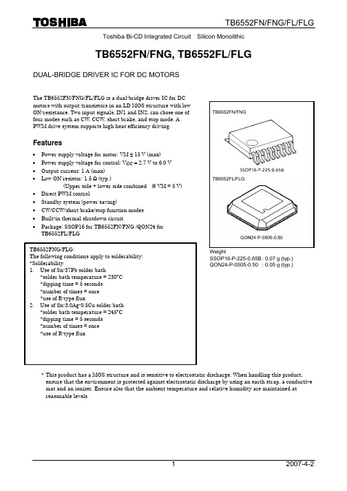
The TB6552FN/FNG/FL/FLG is a dual-bridge driver IC for DC motors with output transistors in an LD MOS structure with low ON-resistance. Two input signals, IN1 and IN2, can chose one of four modes such as CW, CCW, short brake, and stop mode. A PWM drive system supports high heat efficiency driving.
VM VCC VIN IOUT
PD
Topr Tstg
15 V
6
−0.2 to 6
V
IN1, 2, STBY and PWM pins
1
A
0.78 W
(Note 1)
−20 to 85
°C
−55 to 150
°C
Note 1: This rating is obtained when the product is mounted on a 50 × 30 × 1.6 mm glass-epoxy PCB of which 40% or more is occupied by copper.
16
22 Small-signal power supply pin
Remarks GND for small-signal power supply (VCC)
Input PWM signal Ch. A circuit is in standby (power save) state while this signal is Low. Ch. A connect to motor coil pin Ch. A connect to motor coil pin GND for motor power supply (VM) VM (ope) = 2.5 V to 13.5 V Ch. B connect to motor coil pin Ch. B connect to motor coil pin Ch. B circuit is in standby (power save) state while this signal is Low. Input PWM signal
2SJ356-T2中文资料
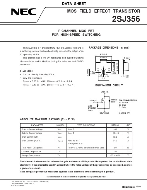
Document No. D11218EJ1V0DS00 (1st edition)Date Published June 1996 PPrinted in Japan19962TYPICAL CHARACTERISTICS (T A = 25 ˚C)DERATING FACTOR OF FORWARD BIAS SAFE OPERATING AREAd T - De r a t i n g F a c t o r -%2510080604020T A - Ambient Temperature - ˚CFORWARD BIAS SAFE OPERATING AREAI D - D r a i n C u r r e n t - A–0.5–10V DS - Drain to Source Voltage - V5075100125150–5–2–1–0.5–0.2–0.1–0.05–1–100–2–5–10–20–502SJ3563DRAIN TO SOURCE ON-STATE RESISTANCE vs.DRAIN CURRENT R D S (o n ) - D r a i n t o S o u r c e O n -S t a t e R e s i s t a n c e - Ω–0.00110.80.60.40.2I D - Drain Current - ADRAIN TO SOURCE ON-STATE RESISTANCE vs.GATE TO SOURCE VOLTAGE R D S (o n ) - D r a i n t o S o u r c e O n -S t a t e R e s i s t a n c e - Ω010.80.60.40.2V GS - Gate to Source Voltage - V–10–0.01–0.1–1–20–2–4–6–8–10–12–14–16–18DRAIN CURRENT vs.DRAIN TO SOURCE VOLTAGEI D - D r a i n C u r r e n t - A–5V DS - Drain to Source Voltage - V TRANSFER CHARACTERISTICS I D - D r a i n C u r r e n t - A–1–10V GS - Gate to Source Voltage - VFORWARD TRANSFER ADMITTANCE vs.DRAIN CURRENT |y f s | - F o r w a r d T r a n s f e r A d m i t t a n c e - S–0.000110I D - Drain Current - ADRAIN TO SOURCE ON-STATE RESISTANCE vs.DRAIN CURRENT R D S (o n ) - D r a i n t o S o u r c e O n -S t a t e R e s i s t a n c e - Ω–0.0011.5I D - Drain Current - A–1–2–3–4–5–4–3–2–1–2–3–4–1–0.1–0.01–0.001–0.0001–0.0000110.10.010.001–0.001–0.01–0.1–110.5–0.01–0.1–1–104TRANSIENT THERMAL RESISTANCE vs. PULSE WIDTHrth(j-a)-TransientThermalResistance-˚C/W1 m1 000100101PW - Pulse Width - s10 m100 m110100Single pulseUsing ceramic substrate of7.5 cm2× 0.7 mmSOURCE TO DRAIN DIODEFORWARD VOLTAGEISD-DiodeForwardCurrent-A–0.2–10–1–0.1–0.01–0.001–0.0001V SD - Source to Drain Voltage - VCAPACITANCE vs.DRAIN TO SOURCE VOLTAGECiss,Coss,Crss-Capacitance-pF–110 0001 00010010V DS - Drain to Source Voltage - V SWITCHING CHARACTERISTICStd(on),tr,td(off),tf-SwitchingTime-ns1 00010010I D - Drain Current - AREVERSE RECOVERY TIME vs.DIODE FORWARD CURRENTtrr-ReverseRecoveryTime-ns–0.051 00010010I F - Diode Forward Current -A–1.2–0.4–0.6–0.8–1.0V GS = 0Pulsed–10–100–1–10–10–0.1–0.5–1–5V GS = 0di/dt = 50 A/ sµREFERENCEDocument Name Document No.NEC semiconductor device reliability/quality control system TEI-1202Quality grade on NEC semiconductor devices IEI-1209 Semiconductor device mounting technology manual C10535EGuide to quality assurance for semiconductor devices MEI-1202 Semiconductor selection guide X10679E5[MEMO]No part of this document may be copied or reproduced in any form or by any means without the prior written consent of NEC Corporation. NEC Corporation assumes no responsibility for any errors which may appear in this document.NEC Corporation does not assume any liability for infringement of patents, copyrights or other intellectual property rights of third parties by or arising from use of a device described herein or any other liability arising from use of such device. No license, either express, implied or otherwise, is granted under any patents, copyrights or other intellectual property rights of NEC Corporation or others.While NEC Corporation has been making continuous effort to enhance the reliability of its semiconductor devices, the possibility of defects cannot be eliminated entirely. To minimize risks of damage or injury to persons or property arising from a defect in an NEC semiconductor device, customer must incorporate sufficient safety measures in its design, such as redundancy, fire-containment, and anti-failure features.NEC devices are classified into the following three quality grades:“Standard“, “Special“, and “Specific“. The Specific quality grade applies only to devices developed based ona customer designated “quality assurance program“ for a specific application. The recommended applicationsof a device depend on its quality grade, as indicated below. Customers must check the quality grade of each device before using it in a particular application.Standard:Computers, office equipment, communications equipment, test and measurement equipment, audio and visual equipment, home electronic appliances, machine tools, personal electronicequipment and industrial robotsSpecial:Transportation equipment (automobiles, trains, ships, etc.), traffic control systems, anti-disaster systems, anti-crime systems, safety equipment and medical equipment (not specifically designedfor life support)Specific:Aircrafts, aerospace equipment, submersible repeaters, nuclear reactor control systems, life support systems or medical equipment for life support, etc.The quality grade of NEC devices in “Standard“ unless otherwise specified in NEC's Data Sheets or Data Books.If customers intend to use NEC devices for applications other than those specified for Standard quality grade, they should contact NEC Sales Representative in advance.Anti-radioactive design is not implemented in this product.M4 94.11。
6MBI225U-120中文资料
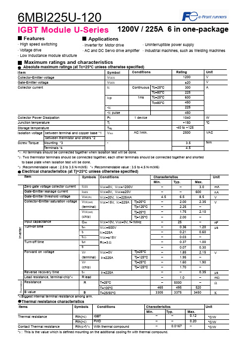
6MBI225U-1201200V / 225A 6 in one-packageFeatures· High speed switching· Voltage drive· Low inductance module structureApplications · Inverter for Motor drive· AC and DC Servo drive amplifierMaximum ratings and characteristicsThermal resistance characteristicsThermal resistanceContact Thermal resistance––0.12––0.20–0.0167 –IGBTFWDWith thermal compound°C/W°C/W°C/W*2 : Two thermistor terminals should be connected together, each other terminals should be connected together and shortedto base plate when isolation test will be done.*3 :Recommendable value : 2.5 to 3.5 N·m(M5) *4 :Recommendable value : 3.5 to 4.5 N·m(M6)Rth(j-c)Rth(j-c)Rth(c-f)*5IGBT Module U-Series*5 : This is the value which is defined mounting on the additional cooling fin with thermal compound.4Items Symbols Conditions Characteristics UnitMin.Typ. Max.· Uninterruptible power supply· Industrial machines, such as Welding machinesCharacteristics (Representative)VGE=0V, f= 1MHz, Tj= 25°CVcc=600V, I=225A, Tj= 25°CCollector current vs. Collector-Emitter voltage (typ.)Tj= 125°C / chipCapacitance vs. Collector-Emitter voltage (typ.)Dynamic Gate charge (typ.)Collector current vs. Collector-Emitter voltage (typ.)Tj= 25°C / chipCollector current vs. Collector-Emitter voltage (typ.)VGE=15V / chipTj=25°C / chipCollector-Emitter voltage vs. Gate-Emitter voltage (typ.)010020030040050060012345C o l l e c t o r c u r r e n t : I c [A ]VGE=20V15V12V10V8V010020030040050060012345C o l l e c t o r c u r r e n t : I c [A ]VGE=20V 15V12V10V8V010020030040050060001234C o l l e c t o r c u r r e n t : I c [A ]Tj=125°CTj=25°C246810510152025C o l l e c t o r - E m i t t e r v o l t a g e : V C E [ V ]Ic=450A Ic=225A Ic= 112.5A0.11.010.0100.0102030C a p a c i t a n c e : C i e s , C o e s , C r e s [ n F ]200400600800100012001400C o l l e c t o r -E m i t t e r v o l t a g e : V C E [ 200V /d i v ]G a t e - E m i t t e r v o l t a g e : V G E [ 5V /d i v]Vcc=600V, Ic=225A, VGE=±15V, Tj= 25°CStray inductance <= 100nHSwitching loss vs. Collector current (typ.)Vcc=600V, VGE=±15V, Rg=3ΩVcc=600V, Ic=225A, VGE=±15V, Tj= 125°C+VGE=15V,-VGE <= 15V, RG >= 3Ω ,Tj <= 125°CSwitching time vs. Collector current (typ.)Vcc=600V, VGE=±15V, Rg=3Ω, Tj=125°CSwitching time vs. Gate resistance (typ.)Switching time vs. Collector current (typ.)Vcc=600V, VGE=±15V, Rg=3Ω, Tj= 25°CReverse bias safe operating area (max.)Switching loss vs. Gate resistance (typ.)10100100010000100200300400S w i t c h i n g t i m e : t o n , t r , t o f f , t f [ n s e c ]Collector current : Ic [ A ]10100100010000100200300400S w i t c h i n g t i m e : t o n , t r , t o f f , t f [ n s e c ]Collector current : Ic [ A ]10100100010000110100S w i t c h i n g t i m e : t o n , t r , t o f f , t f [ n s e c ]Gate resistance : Rg [ Ω ]trtftoffton 01020304050100200300400500S w i t c h i n g l o s s : E o n , E o f f , E r r [ m J /p u l s e ]Collector current : Ic [ A ]Eon(125°C)Eon(25°C)Eoff(125°C)Err(125°C)Err(25°C)Eoff(25°C)0255075100125150110100S w i t c h i n g l o s s : E o n , E o f f , E r r [ m J /p u l s e ]Gate resistance : Rg [ Ω ]EoffErrEon0100200300400500600200400600800100012001400C o l l e c t o r c u r r e n t : I c [ A ]Collector - Emitter voltage : VCE [ V ]Transient thermal resistance (max.)Reverse recovery characteristics (typ.)Vcc=600V, VGE=±15V, Rg=3ΩForward current vs. Forward on voltage (typ.)chipTemperature characteristic (typ.)01002003004005006001234F o r w a r d c u r r e n t : I F [ A ]Forward on voltage : VF [ V ]Tj=125°CTj=25°C101001000100200300400500R e v e r s e r e c o v e r y c u r r e n t : I r r [ A ]R e v e r s e r e c o v e r y t i m e : t r r [ n s e c ]Forward current : IF [ A ]Irr (125°C)Irr (25°C)trr (125°C)trr (25°C)0.0010.0100.1001.0000.0010.0100.1001.000T h e r m a l r e s i s t a n s e : R t h (j -c ) [ °C /W ]Pulse width : Pw [ sec ]0.1110100-60-40-20020406080100120140160180Temperature [°C ]R e s i s t a n c e : R [ k Ω ]Outline Drawings, mmM6296MBI225U-120IGBT ModuleEquivalent Circuit Schematic[Thermister]135111210987246[Inverter]。
BS 6500 中文

-1-
BS 6500:2000
2
表 8— 无 表 9— 无 表 10— 轻型橡胶绝缘、编织软线,300/300V,圆形双芯和 3 芯 表 11— 轻型橡胶绝缘、编织 UDF 线,300/300V,圆形双芯和 3 芯 表 12— 裸型橡胶绝缘和铠装(护套)软线,300/500V,圆形双芯、3 芯、4 芯和 5 芯 表 13— 裸型橡胶绝缘,PCP 或相等的人造橡胶铠装(护套)软线,300/500V,圆形双芯、 3芯 表 14— 裸型橡胶绝缘、铠装(护套)、屏蔽和铠装(护套)软线,300/500V,圆形双芯、3 芯、4 芯和 5 芯 表 15— 裸型耐 90℃EPR 热或类似人造橡胶绝缘和铠装(护套)软线,300/500V,圆形双 芯、3 芯、4 芯和 5 芯 表 16— 裸型耐 90℃EPR 热或类似人造橡胶绝缘和 CSP 或类似人造橡胶铠装(护套)软线, 300/500V,圆形双芯、3 芯和 4 芯 表 17— 高弹性橡胶绝缘和铠装(护套)电线,300/500V,圆形双芯和 3 芯 表 18— 高弹性橡胶绝缘,交接 PVC(XLPVC)铠装(护套)电线,300/300V,圆形双芯 和3芯 表 19— 高弹性交接 PVC(XLPVC)绝缘和铠装(护套)电线,300/300V,圆形双芯和 3 芯 表 20— 无 表 21— 无 表 22— 无 表 23— 无 表 24— PVC 绝缘(箔线)软线,平行双线,300/300V 表 25— PVC 绝缘软线,平行双线,300/300V 表 26— 轻型 PVC 绝缘和铠装(护套)软线,平行双线,300/300V,圆形双芯、3 芯、4 芯 和5芯 表 27— 裸型 PVC 绝缘和铠装(护套)软线,平行双线,300/500V,圆形双芯、3 芯和 4 芯 表 28— 轻性 90℃PVC 绝缘和铠装(护套)软线,平行双线,300/300V,圆形双芯、3 芯和 4芯 表 29— 裸型 90℃PVC 绝缘和铠装(护套)软线,平行双线,300/500V,圆形双芯、3 芯、
2SD2568中文资料(rohm)中文数据手册「EasyDatasheet - 矽搜」
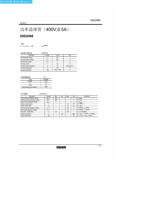
0.5 (A)
1
0.5 (A)
1
0.02 BASE SATURATION VOLTAGE : V 0.01 0.001 0.002 0.005 0.01 0.02 0.05 0.1 0.2 COLLECTOR CURRENT : I
C
0.5 (A)
1
COLLECTOR CURRENT : I
图4 DC电流增益 - 集电极电流(
1/2
芯片中文手册,看全文,戳
2SD2568
晶体管电气特Biblioteka 曲线200 (mA) 160
C
Ta=25 C
mA 3.0m A 2.5m A 2.0m A 1.5m A
1 (A)
C
V CE =3V
FE
1000 500 200 100
Ta=25 C
0.5 0.2 0.1 0.05
25°C
FE
2SD2568 CPT3 PQ TL 2500
电气特性
Parameter Collector-base breakdown voltage Collector-emitter breakdown voltage Emitter-base breakdown voltage Collector cutoff current Emitter cutoff current Collector-emitter saturation voltage Base-emitter saturation voltage DC current transfer ratio Transition frequency Output capacitance
(V) 2
BE(sat)
200 100 50 20
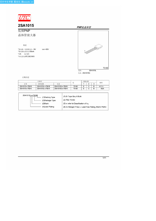
2SA1015中文资料(Unisonic Technologies)中文数据手册「EasyDatasheet - 矽搜」
BL 350-700
2of 4
芯片中文手册,看全文,戳
2SA1015
典型特征
静态特性
-50
-40
I =-300µA
-30 I =-250µA
-20
I =-200µA
I =-150µA
-10
I =-100µA
I =-50µA
0
-0
-4 -8 -12 -16 -20
集电极 - 发射极电压,BV
饱和电压
-10 I =10xI
-10 -10 (mA)
-10
V
-10
V
-10 -10
-10 -10 集电极电流,I
集电极输出电容
-10 f=1MHz -10 I =0
-10 -10 (mA)
-10
-10
-10
-10
-10
-10
集电极基极电压,BV
-10 (V)
3of 4
芯片中文手册,看全文,戳
4of 4
FE1
Y 120-240
GR 200-400
额定值
单元
-50
V
-50
V
-5
V
-150
mA
-50
mA
400
mW
125
°C
-55 ~ +125
°C
MIN TYP 最大单位
-50
V
-50
V
-5
V
-100 nA
-100 nA
120
700
25
-0.1 -0.3 V
-1.1 V
4.0 7.0 pF
80
MHz
0.5 6 dB
MMSZ5232BT1中文资料
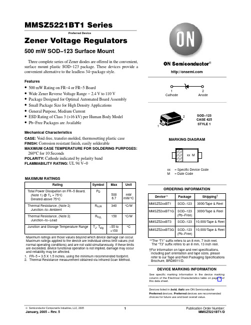
MMSZ5221BT1 SeriesPreferred DeviceZener Voltage Regulators 500 mW SOD−123 Surface MountThree complete series of Zener diodes are offered in the convenient, surface mount plastic SOD−123 package. These devices provide a convenient alternative to the leadless 34−package style.Features•500 mW Rating on FR−4 or FR−5 Board•Wide Zener Reverse V oltage Range − 2.4 V to 110 V •Package Designed for Optimal Automated Board Assembly •Small Package Size for High Density Applications •General Purpose, Medium Current•ESD Rating of Class 3 (>16 kV) per Human Body Model•Pb−Free Packages are AvailableMechanical CharacteristicsCASE:V oid-free, transfer-molded, thermosetting plastic case FINISH:Corrosion resistant finish, easily solderableMAXIMUM CASE TEMPERATURE FOR SOLDERING PURPOSES: 260°C for 10 SecondsPOLARITY:Cathode indicated by polarity band FLAMMABILITY RATING:UL 94 V−0MAXIMUM RATINGSMaximum ratings are those values beyond which device damage can occur. Maximum ratings applied to the device are individual stress limit values (not normal operating conditions) and are not valid simultaneously. If these limits are exceeded, device functional operation is not implied, damage may occur and reliability may be affected.1.FR−5 = 3.5 X 1.5 inches, using the minimum recommended footprint.2.Thermal Resistance measurement obtained via infrared Scan Method.See specific marking information in the device marking column of the Electrical Characteristics table on page 3 of this data sheet.DEVICE MARKING INFORMATIONDevices listed in bold, italic are ON Semiconductor Preferred devices. Preferred devices are recommended choices for future use and best overall value.ELECTRICAL CHARACTERISTICS (T A = 25°C unlessotherwise noted, V= 0.95 V Max. @ I = 10 mA)4.Nominal Zener voltage is measured with the device junction in thermal equilibrium at T L = 30°C $1°C.5.Z ZT and Z ZK are measured by dividing the AC voltage drop across the device by the ac current applied.The specified limits are for I Z(AC) = 0.1 I Z(dc) with the AC frequency = 1 KHz.V Z , NOMINAL ZENER VOLTAGE (V)−1012345678Figure 1. Temperature Coefficients (Temperature Range −55°C to +150°C)100101V Z , NOMINAL ZENER VOLTAGE (V)Figure 2. Temperature Coefficients (Temperature Range −55°C to +150°C)1.21.00.80.60.40.20T, TEMPERATURE (°C)Figure 3. Steady State Power Derating PW, PULSE WIDTH (ms)Figure 4. Maximum Nonrepetitive Surge Power1000100101V Z , NOMINAL ZENER VOLTAGEFigure 5. Effect of Zener Voltage onZener Impedance100101V F , FORWARD VOLTAGE (V)Figure 6. Typical Forward Voltage1000100101q V Z , T E M P E R A T U R E C O E F F I C I E N T (m V /°C )q V Z , T E M P E R A T U R E C O E F F I C I E N T (m V /°C )P p k , P E A K S U R G E P O W E R (W A T T S )Z Z T , D Y N A M I C I M P E D A N C E (W )I F , F O R W A R D C U R R E N T (m A )C , C A P A C I T A N C E (p F )V Z , NOMINAL ZENER VOLTAGE (V)Figure 7. Typical Capacitance 1000100101V Z , ZENER VOLTAGE (V)1001010.10.01V Z , ZENER VOLTAGE (V)1001010.10.01V Z , NOMINAL ZENER VOLTAGE (V)Figure 8. Typical Leakage CurrentFigure 9. Zener Voltage versus Zener Current(V Z Up to 12 V)Figure 10. Zener Voltage versus Zener Current(12 V to 91 V)I R , L E A K A G E C U R R E N T (m A )I Z , Z E N E R C U R R E N T (m A )I Z , Z E N E R C U R R E N T (m A )PACKAGE DIMENSIONSSOD−123CASE 425−04ISSUE Cǒmm inchesǓSCALE 10:1*For additional information on our Pb−Free strategy and solderingdetails, please download the ON Semiconductor Soldering and Mounting Techniques Reference Manual, SOLDERRM/D.SOLDERING FOOTPRINT*ON Semiconductor and are registered trademarks of Semiconductor Components Industries, LLC (SCILLC). SCILLC reserves the right to make changes without further notice to any products herein. SCILLC makes no warranty, representation or guarantee regarding the suitability of its products for any particular purpose, nor does SCILLC assume any liability arising out of the application or use of any product or circuit, and specifically disclaims any and all liability, including without limitation special, consequential or incidental damages.“Typical” parameters which may be provided in SCILLC data sheets and/or specifications can and do vary in different applications and actual performance may vary over time. All operating parameters, including “Typicals” must be validated for each customer application by customer’s technical experts. SCILLC does not convey any license under its patent rights nor the rights of others. SCILLC products are not designed, intended, or authorized for use as components in systems intended for surgical implant into the body, or other applications intended to support or sustain life, or for any other application in which the failure of the SCILLC product could create a situation where personal injury or death may occur. Should Buyer purchase or use SCILLC products for any such unintended or unauthorized application, Buyer shall indemnify and hold SCILLC and its officers, employees, subsidiaries, affiliates,and distributors harmless against all claims, costs, damages, and expenses, and reasonable attorney fees arising out of, directly or indirectly, any claim of personal injury or death associated with such unintended or unauthorized use, even if such claim alleges that SCILLC was negligent regarding the design or manufacture of the part. SCILLC is an Equal Opportunity/Affirmative Action Employer. This literature is subject to all applicable copyright laws and is not for resale in any manner.PUBLICATION ORDERING INFORMATION。
E6B2编码器 文档

旋转式编码器概要旋转式编码器概要旋转式编码器的定义旋转式编码器,是将旋转的机械位移量转换为电气信号,对该信号进行处理后检测位置速度等的传感器。
检测直线机械位移量的传感器称为线性编码器。
特长①根据轴的旋转变位量进行输出通过联合器与轴结合,能直接检测旋转位移量。
;②启动时无需原点复位。
(仅绝对型)绝对型的情况下,将旋转角度作为绝对数值进行并列输出。
③可对旋转方向进行检测。
增量型中可通过A相和B相的输出时间,绝对型中可通过代码的增减来掌握旋转方向。
④请根据丰富的分辨率和输出型号,选择最合适的传感器。
根据要求精度和成本、连接电路等,选择适合的传感器。
旋转式编码原理分类选择要点增量式或绝对式考虑到容许的成本,电源接通时的原点可否恢复、控制速度、耐干扰性等,选择合适的类型。
分解率精度的选择在考虑组装机械装置的要求精度和机械的成本的基础上,选择最适合的产品。
一般选择机械综合精度的1/2~1/4精度的分辨率。
外形尺寸选定时还要考虑安装空间与选定轴的形态(中空轴、杆轴类)。
轴容许负重选定时要考虑到不同安装方法的不同轴负载状态、及机械的寿命等。
容许最大旋转数根据使用时的机械的最大旋转数来选择。
最高响应频率数根据组装机械装置使用时的轴最大旋转数来定。
最大响应频率=(旋转数/60)×分辨率但是,由于实际的信号周期有所波动,所以选定时应针对上述的计算值,来选择留有余度的规格。
保护构造∙根据使用环境中的灰尘、水、油等的程度来选择。
∙仅灰尘:IP50∙还有水、油:IP52(f)、IP64(f)(防滴落、防油)轴的旋转启动转矩驱动源的转矩为多少?输出电路方式选择电路方式时应考虑到连接的后段机器、信号的频率、传送距离、干扰环境等。
长距离传送的情况下,选择线路驱动器输出。
术语解说分辨率轴旋转1次时输出的增量信号脉冲数或绝对值的绝对位置数。
输出相增量型式的输出信号数。
包括1相型(A相)、2相型(A相、B相)、3相(A相、B相、Z相)。
ABB UBB 型有载分接开关 用户手册说明书

UBB 型有载分接开关用户手册1ZSE 5492-156 zh, Rev. 4初版说明本指南中提供的信息仅适用于常规情况,并不能涵盖所有可能的应用。
有关本指南未涵盖的任何具体应用的问题,请直接向 ABB 或其授权代表咨询。
ABB 对本指南中信息的准确性及此类信息的使用不做任何保证或陈述,亦不承担任何责任。
本指南中的信息如有变更,恕不另行通告。
未经书面许可,不得复制本文件,并且其内容不得透露给第三方,亦不得用于任何未经授权之目的。
违者必究。
制造商ABB ABComponentsSE-771 80 LUDVIKASweden在此声明如下:产品型号UB 型有载分接开关及BUE 型和 BUL 型电机驱动机构遵守以下要求:在设计方面,考虑到此机械装置作为油浸电力变压器的一个组件,特需遵守如下要求• 机械规范 89/392/EEC(91/368/EEC 和 93/44/EEC 修正版)和 93/68/EEC(标志)中规定的,变压器制造商必须正确地实施前述产品的安装及电气连接(例如,按照我们的安装指南进行操作);• EMC 规范 89/336/EEC 中关于辐射方面内在特征和抗干扰水平的规定;以及• 低电压规范 73/23/EEC(由 93/68/EEC 规范修正)中关于内置式电机和控制电路器件的规定。
特此声明:除非使用此机械装置的整套设备已被证明满足机械规范的要求,否则本机械装置不得投入使用。
日期 2013-02-15签署人 .........................................................................Hans Linder职务本地产品组单元部件分接开关产品经理4 用户手册 UBB | 1ZSE 5492-156 zh, Rev. 4概述ABB 公司生产的 UB 型有载分接开关是经过多年开发研制而成,能给用户提供最大的可靠性。
简洁与坚固的结构,使其使用寿命等于变压器的使用寿命,并用最少的维护工作便能保证有载分接开关的可靠运行。
ZMM5252B中文资料(WILLAS ELECTRONIC)中文数据手册「EasyDatasheet - 矽搜」
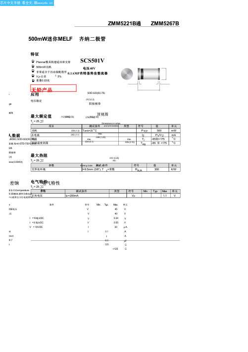
5264
ZMM5265B
62.0
58.90
65.10
185
2.0
1400
0.25
0.1
47.0
5265
ZMM5266B
68.0
64.60
71.40
230
1.8
1600
0.25
0.1
52.0
5266
ZMM5267B
75.0
71.25
78.75
270
1.7
1700
0.25
0.1
56.0
5267
1)基于直流测量达到热平衡;引线长度=9.5毫米(3/8");散热器= 30K / W热阻
5244
ZMM5245B
15.0
14.25
15.75
16
8.5
600
0.25
0.1
11.0
5245
ZMM5246B
16.0
15.20
16.80
17
7.8
600
0.25
0.1
12.0
5246
ZMM5247B
17.0
16.15
17.85
19
7.4
600
0.25
0.1
13.0
5247
ZMM5248B
18.0
类型
max. .006 (0.15)
符号
PTOT IZ Tj Tstg
值
500
PV/V Z -65到+175 –65 至 +175
单元
mW
mA °C °C
.010 (0.25) min.
Marking Code: 测JV o试r 4条件
MP-B2母板说明书

Assembly Instructions MP-B2 Mother BoardIntroductionThe MP-B2 Mother Board is a 9 " x 14" double sided plated thru hole board onto which all of the various processor boards are plugged. Provisions have been made for one processor board, up to four memory boards plus two unused slots. This gives the user the ability to handle up to 32K words of memory.The mother board also provides the line buffering and address decoding for up to eight interface boards. Although one of the eight must be the serial control interface, the other seven may be any com-bination of serial (MP-S) and parallel (MP-L) interfaces the user may choose to have. For those demanding even more interfaces the 50-line processor bus may be paralleled onto another MP-B2 Mother Board with power supply expanding the interfacing to one serial control interface, plus any combination of up to fifteen serial (MP-S) and parallel (MP-L) interfaces. Doing this requires a minor modification to the second mother board.When the SWTPC 6800 Computer System is being assembled, work on only one board at a time. Each of the system's boards and their associated parts must not be intermixed to avoid confusion during assembly.PC Board AssemblyNOTE: Since all of the holes on the PC board have been plated thru, it is only necessary to solder the components from the bottom side of the board. The plating provides the electrical connection from the "BOTTOM" to the "TOP" foil of each hole. Unless otherwise noted it is important that none of the con-nections be soldered until all of the components of each group have been installed on the board. This makes it much easier to interchange components if a mistake is made during assembly. Be sure to use a low wattage iron (not a gun) with a small tip. Do not use acid core solder or any type of paste flux. We will not guarantee or repair any kit on which either product has been used. Use only the solder supplied with the kit or a 60/40 alloy resin core equivalent. Remember all of the connections are soldered on the bottom side of the board only. The plated-thru holes provide the electrical connection to the top foil. ( ) Before installing any parts on the circuit board, check both sides of the board over carefully for incomplete etching and foil "bridges" or "breaks". It is unlikely that you will find any but shouldthere be one, especially on the "TOP" side of the board, it will be very hard to locate and correct after all of the components have been installed on the board.( ) Attach all of the resistors to the board. As with all other components unless noted, use the parts list and component layout drawing to locate each part and install from the "TOP" side of the board bending the leads along the "BOTTOM" side of the board and trimming so that 1/16" to 1/8" of wire remains. Solder.( ) Install all of the capacitors on the board. Solder.( ) Install each of the 59, 10-pin Molex male connectors oriented so the shorter pinned side fits into the holes provided on the mother board. These connectors must be inserted from the "TOP" side of the board and must be pressed down firmly against the board. Make sure the body of theconnector seats firmly against the circuit board and that each pin extends completely into theholes on the circuit board. Not being careful here will cause the plug-on boards to be less rigid.Do not solder the pins adjacent the dotted lines shown in the component layout drawing. It issuggested that you solder only the two end pins of each of the fifty-nine connectors until all have been installed; at which time, if everything looks straight and rigid, you should solder the as yet unsoldered pins still excluding the ones adjacent the dotted lines on the component layoutdrawing.( ) Using a pair of wire cutters, cut off the "INDEX" pin on each of the seven main board and eight interface board male connector strips. Each row is pointed out by the word "INDEX" printed right on the "TOP" side of the mother board. Be very careful when doing this. Do not cut off anything other than the "INDEX" pins. You cannot afford to make a mistake here. These "INDEX" locations prevent the various plug-on boards from being plugged on incorrectly later during assembly.( ) Install each of the integrated circuits excluding IC2. As each one is installed make sure it is down firmly against the board and solder only two of the leads to hold the pack in place while the other IC's are being inserted. Be very careful to install each in its correct position. Do not bend theleads on the back side of the board. Doing so makes it very difficult to remove the integratedcircuits should replacement ever be necessary. The semicircle notch or dot on the end of thepackage is used for orientation purposes and must match with the outlines shown on thecomponent layout drawing for each of the IC's. After inserting all of the integrated circuits go back and solder each of the as yet unsoldered pins.( ) Install integrated circuit IC2 on the circuit board. This component must be oriented so its metal face is facing the circuit board with the small metal heatsink sandwiched between the two. The heatsink and IC are secured to the circuit board with a #4-40 x 3/8" screw, lockwasher and nut.The three leads of the integrated circuit must be bent down into each of their respective holes and the heatsink must be orientated as shown in the component layout drawing. Solder.( ) Remove any oxidation from the copper on the two mother board support strips using a piece of Scotchbrite. Take the shorter of the two and position it on the "BOTTOM" side of the motherboard along the main board GND bus and perpendicular to the mother board as indicated in the component layout drawing. It should be oriented with its copper edges against the "BOTTOM"side of the mother board, extending from the first to the seventh main board connection rows.Solder the as yet unsoldered connector pins adjacent the strip making sure the strip is soldered in place as well. Make sure the strip remains firmly against the PC board while soldering. Now take the longer of the two strips and position it against the "BOTTOM" side of the mother boardparallel to and in the center of the +8 UNR interface bus as indicated in the component layout drawing and attach like the first strip. These strips provide rigidity and support for the motherboard and prevent the mother board from bottoming out when the plug-on boards are installed. ( ) Working from the "TOP" side of the circuit board, fill in all of the feed-thru's with molten solder.The feed-thru's are those unused holes o n the board whose internal plating connects the "TOP"and " BOTTOM " circuit connections. Filling these feed-thru's with molten solder guarantees the integrity of the connections and increases the current handling capability. Do not fill in the 16holes on the edge of the board that are to be used for wiring connections.( ) Now that all of the components have been installed on the board, double check to make sure alI have been installed correctly in their proper location.( ) Check very carefully to make sure that all connections have been soldered. It is very easy to miss some connections when soldering which can really cause some hard-to-find problems later during checkout. Also, look for solder "bridges" and "cold" solder joints which are another common pro-blem.This completes the assembly phase for the MP-B2 board. Checkout instructions for the board are provided with the System Checkout Instructions supplied with this kit. The System Checkout Instructions are used after having assembled the processor board, M P-B 2 mother board, serial control interface and the M PM P-P power supply.How It WorksThe only circuitry on the MP-B2 mother board is that tying the various interface cards to the system's interface information bus. IC1 is a non-inverting buffer used to drive selected control lines feeding the interface cards. One of eight decoders IC3 and IC6 decode and enable one of eight interface cards when one of the interface addresses is loaded to the 50-line system information bus.Since the eight bit data bus for the main boards as well as the interface cards is bi-directional, transceiver buffers IC7 and IC8 buffer the incoming and outgoing data to and from the interface data bus to the system's data bus. Gates within NAND gate IC4 and NOR gate IC5 control the direction of data flow within the transceiver/buffers. +5 VDC power for the interface decode/buffer circuitry is provided by voltage regulator IC2. +5 VDC power for all of the plug-on boards, including interfaces, is provided by separate regulators on each board.The following is a brief description of each of the fifty lines on the system information bus:D0 - D7# The D0 - D7# lines carry inverted data bits 0 thru 7 respectively forming 8-bit data words which are exchanged between the various boards within the system.A0 - A15 The A0 - A15 lines carry address bits 0 thru 15 respectively forming a 16-bit address which is used to define either a memory location or interface address.GND The GND line is the system's common or power supply ground point.7- 8VDC UNREG or +8 UNR The 7 - 8 VDC UNREG point is the line to which a +7 to 8 volt DC @10A unregulated power supply should be attached. This voltage is then regulated down to +5 VDC by in dependent regulators on the various boards within the system.-12, +12 The -12 and +12 points are lines to which an isolated ground -12@200 Ma and +12 @200 Ma power supply should be connected. The voltages are necessary forgenerating the currents required by 20 Ma current loop and RS-232 equipment onthe serial interfaces.INDEX The INDEX is an unused bus and is provided so the pin on each of the male connectors may be cut with the corresponding female connector pins plugged,preventing the circuit boards from being plugged on incorrectlyM. RESET#The MANUAL RESET# line when momentarily grounded indirectly resets the registers internal to the processor and interfaces, and loads the ROM storedmini-operating system. This line is normally grounded by depressing the RESETbutton on the system's front panel.NMI# The NMI# is the non-maskable, single level interrupt line feeding the processor board. When momentarily grounded it forces the processor into a push-down stack,store routine, followed by a program jump to a user selected address stored in theoperating system RAM. The NMI# is non-maskable thus, can not be inhibited by theprogrammer thru software.IRQ# The IRQ# is the maskable, single level interrupt request line feeding the processor board. If not inhibited by software it will, when momentarily grounded, force theprocessor into a push-down stack, store routine followed by a program jump to a userselected address stored in the operating system RAM.UD1, UD2 The UD1 and UD2 are user defined lines and have not been assigned a function.ø2 ø2 is one of the two complementary system clock outputs and is used to signal that valid data is on the data lines D0 - D7# when low.VMA# VMA# is the valid memory address line which goes low to confirm that valid memory data is being presented on the sixteen address lines, A0 - A15.R /W The READ/WRITE line establishes the direction of data flow on the eight data lines, D0 -D7. It is high for a read from memory or interface and low for a write to memoryor interface.RESET# The RESET line when low resets the registers internal to the processor and interfaces, and loads the ROM stored mini-operating system. This line is activated bya one-shot on the processor board when the system is first powered up or when M.RESET line is momentarily groundedBA The BUS AVAILABLE line goes high acknowledging a processor halt meaning the processor has stopped and that the system information bus is available for externalcontrol.HALT# The normally high HALT# line when brought low, halts the processor and frees the system information bus for external controlø1 ø1 is the non-overlapping clock complement of ø2. This signal is provided by the MP-A but not by the MP-A2 processor board.110b, 150b 300b, 600b, 1200b These five lines carry the clocks required by the serial interfaces for 110, 150, 300, 600, 1200 baud communication.Attached to the 50-line system information bus are the interface decode and driver circuits. A considerable cost savings is made by providing the address decoding and information bus buffering for all of the interfaces right on the mother board instead of providing it on each of the interface boards individually. Since each of the parallel interfaces require four address locations and the serial two, four addresses are provided for each of the interface positions. They are assigned as shown in the memory map, figure 1. Interface position 1 (8004 - 8007) is reserved for the terminal, control interface. The signals carried on the interface information bus are almost identical to those on the system bus. UD3 and UD4 are here again User Defined data lines and RS0 and RS1 are Register select lines which are identical to address line A0 and A1 respectively.The original MP-B Mother Board decoded the entire 8 K block of memory from 32K thru 40K as being resident on the mother board. Although simpler from a circuitry viewpoint, this technique was wasteful and has been changed on this version, the MP-B2, so that only the 32K thru 36K block has been allocated to the mother board interface addresses. This allows boards outside the interface address range to use the 36K thru 40K memory addresses.The new decoding arrangement also makes it easy to reassign the interface address block to any 4K region from 32K to 64K in 4K increments. Although this isn't allowable when using the MIKBUG® or SWTBUG® monitors, it does have potential when using custom monitors.To relocate the 4K interface address block to something other than the 32K thru 36K hardwired assignment, carefully cut the foil trace going to pin 15 of IC6 on the bottom side of the MP-B2 board. Jumper pin 12 of IC5 to the specified pin of IC6 using the table below:Interface Address Assignment IC6 pin #32K - 36K (8000-8FFF) 1536K - 40K (9000-9FFF) 1440K - 44K (A000-AFFF) 1344K - 48K (B000-BFFF) 1248K - 52K (C000-CFFF) 1152K - 56K (D0D0-DFFF) 1056K - 60K (E000-EFFF) 960K - 64K (F000-FFFF) 7The actual interface card addresses will be the first 32 addresses of each 4K block with four sequential addresses assigned to each card position.If you ever wish to expand your system to two MP-B2 mother boards in order to accommodate more interface cards, you must first modify the second MP-B2 board so it responds to the second set of 32 sequential addresses within the 4 K address block. The second MP-B2 board should also be assigned the same 4 K memory address block as the first MP-B2 board. Modify the second MP-B2 mother board by cutting the foil trace going to pin 4 of IC6 right at IC6. Now run a jumper from pin 4 of IC6 to pin 4 of IC5. The MP-B2 mother boards themselves are interconnected by paralleling the 50-pin buses together using #18 gauge or heavier stranded wire. The wire length should be kept as short as possible and preferably no more than 24 inches in length.NOTE: The MP-A2 Processor board does not generate the ø1 signal described in the mother board bus line definitions when plugged onto the M P-B mother board.MIKBUG ® is a registered trademark of Motorola, Inc.SWTBUG® is a registered trademark of Southwest Technical Products Corp.Resistors___ R1 470 ohm 1/4 watt resistor ___ R7 6.8K ohm 1/4 watt resistor ___ R2 470 ohm 1/4 watt resistor ___ R8 6.8K ohm 1/4 watt resistor ___ R3 470 ohm 1/4 watt resistor ___ R9 1K ohm 1/4 watt resistor ___ R4 470 ohm 1/4 watt resistor ___ R10 470 ohm 1/4 watt resistor ___ R5 470 ohm 1/4 watt resistor ___ R11 1K ohm 1/4 watt resistor ___ R6 470 ohm 1/4 watt resistorCapacitors___ C4 0.1 mfd disk capacitorIntegrated Circuits___IC1 DM8097 / 74367 / 74LS367 ___IC5 7402 Quad NOR Gate___IC2 7805 +5VDC Voltage Regulator ___IC6 74S138 1 of 8 decoder___IC3 74S138 1 of 8 decoder ___IC7 DM8835 / DS8835___IC4 7400 Quad NAND Gate ___IC8 DM8835 / DS8835。
爱森摩尔Z5型号超压保护器说明说明书

Eaton 210075Eaton Moeller® series Z5 Overload relay, Ir= 200 - 250 A, 1 N/O, 1 N/C, For use with: DILM250, DILM300AGeneral specificationsEaton Moeller® series Z5 Thermal overload relay2100754015082100759Z5-250/FF250146 mm 167 mm 128 mm 1.727 kgIEC/EN 60947UL Category Control No.: NKCR VDE 0660 CECSA Class No.: 3211-03 ULCSA-C22.2 No. 60947-4-1-14 CSA File No.: 012528 UL 60947-4-1 UL File No.: E29184 IEC/EN 60947-4-1 CSAProduct NameCatalog Number EANModel Code Product Length/Depth Product Height Product Width Product Weight CertificationsReset pushbutton manual/autoTrip-free releaseTest/off buttonPhase-failure sensitivity (according to IEC/EN 60947, VDE 0660 Part 102)-25 °C60 °C25 °C40 °CCLASS 10 ADamp heat, constant, to IEC 60068-2-78Damp heat, cyclic, to IEC 60068-2-30IP00Separate mountingDirect mountingDirect attachment/single positioning200 A250 AIII3Overload relay Z5With terminal cover, Protection against direct contact when actuated from front (EN 50274)4000 V (auxiliary and control circuits)8000 V ACFeatures Ambient operating temperature - minAmbient operating temperature - maxAmbient operating temperature (enclosed) - minAmbient operating temperature (enclosed) - maxClassClimatic proofingDegree of protectionMounting methodOverload release current setting - minOverload release current setting - maxOvervoltage categoryPollution degreeProduct categoryProtectionRated impulse withstand voltage (Uimp)Shock resistance10 g, Mechanical, Sinusoidal, Shock duration 10 ms Branch circuits, (UL/CSA)≤ 0.25 %/K, residual error for T > 40° Continuous 25 mm width, Main connection185 mm²2 x (0.75 - 2.5) mm², Control circuit cables1 x (0.75 - 2.5) mm², Control circuit cables1 x (0.75 - 4) mm², Control circuit cables2 x (0.75 - 4) mm², Control circuit cables2/0 - 500 MCM, Main cables2 x (18 - 14), Control circuit cables185 mm²16 mm (Hexagon head spanner SW)8 mmM10 x 35, Terminal screw, Main connectionsM3.5, Terminal screw, Control circuit cables1 x 6 mm, Terminal screw, Control circuit cables, Standard screwdriver2, Terminal screw, Control circuit cables, Pozidriv screwdriver18 Nm, Main cable connection screw/bolt1.2 Nm, Screw terminals, Control circuit cables6 A 1.5 A 1200 A Class L, max. Fuse, SCCR (UL/CSA) 18 kA, SCCR (UL/CSA)1200 A, max. CB, SCCR (UL/CSA)500 A gG/gL, Fuse, Type “1” coordinationSuitable forTemperature compensationTerminal capacity (busbar)Terminal capacity (flexible with cable lug)Terminal capacity (flexible with ferrule)Terminal capacity (solid)Terminal capacity (solid/stranded AWG)Terminal capacity (stranded with cable lug)Width across flatsStripping length (control circuit cable)Screw sizeScrewdriver sizeTightening torqueConventional thermal current ith of auxiliary contacts (1-pole,open)Rated operational current (Ie) at AC-15, 120 VShort-circuit current rating (basic rating)Short-circuit protection rating1.5 A0.9 A0.4 A0.2 A0.9 A0.75 A1000 V440 V, Between auxiliary contacts and main contacts, According to EN 61140240 V AC, Between auxiliary contacts, According to EN 61140 500 V AC, Between main circuits, According to EN 61140R300, DC operated (UL/CSA)B300 at opposite polarity, AC operated (UL/CSA)B600 at opposite polarity, AC operated (UL/CSA)600 VAC600 VAC 500 A gG/gL, Fuse, Type “2” coordinationMax. 6 A gG/gL, fuse, Without welding, Auxiliary and control circuits111143.5 W0 W14.5 W250 A0 WMeets the product standard's requirements.Meets the product standard's requirements.Meets the product standard's requirements.Meets the product standard's requirements.Rated operational current (Ie) at AC-15, 220 V, 230 V, 240 V Rated operational current (Ie) at AC-15, 380 V, 400 V, 415 V Rated operational current (Ie) at DC-13, 110 VRated operational current (Ie) at DC-13, 220 V, 230 V Rated operational current (Ie) at DC-13, 24 VRated operational current (Ie) at DC-13, 60 VRated operational voltage (Ue) - maxSafe isolationSwitching capacity (auxiliary contacts, pilot duty) Voltage rating - maxVoltage rating - max Number of auxiliary contacts (change-over contacts)Number of auxiliary contacts (normally closed contacts) Number of auxiliary contacts (normally open contacts) Number of contacts (normally closed contacts)Number of contacts (normally open contacts)Equipment heat dissipation, current-dependent PvidHeat dissipation capacity PdissHeat dissipation per pole, current-dependent PvidRated operational current for specified heat dissipation (In) Static heat dissipation, non-current-dependent Pvs10.2.2 Corrosion resistance10.2.3.1 Verification of thermal stability of enclosures10.2.3.2 Verification of resistance of insulating materials to normal heat10.2.3.3 Resist. of insul. mat. to abnormal heat/fire by internal elect. effectsMeets the product standard's requirements.Does not apply, since the entire switchgear needs to be evaluated.Does not apply, since the entire switchgear needs to be evaluated.Meets the product standard's requirements.Does not apply, since the entire switchgear needs to be evaluated.Meets the product standard's requirements.Does not apply, since the entire switchgear needs to be evaluated.Does not apply, since the entire switchgear needs to be evaluated.Is the panel builder's responsibility.Is the panel builder's responsibility.Is the panel builder's responsibility.Is the panel builder's responsibility.Is the panel builder's responsibility.The panel builder is responsible for the temperature rise calculation. Eaton will provide heat dissipation data for the devices.Is the panel builder's responsibility. The specifications for the switchgear must be observed.Product Range Catalog Switching and protecting motorseaton-tripping-devices-z5-overload-relay-characteristic-curve-003.eps eaton-tripping-z5-overload-relay-characteristic-curve.epsDA-DC-00004856.pdfDA-DC-00004846.pdfeaton-tripping-devices-overload-relay-z5-overload-relay-dimensions-002.epseaton-tripping-devices-overload-relay-z5-overload-relay-3d-drawing.epsDA-CE-ETN.Z5-250_FF250IL03407006ZIL026005ZUIL03407081ZDA-MN-h1476dgbDA-CS-z5_ff250DA-CD-z5_ff250eaton-general-release-zeb-overload-relay-wiring-diagram.epseaton-tripping-devices-overload-relay-zeb-overload-relay-wiring-diagram.eps10.2.4 Resistance to ultra-violet (UV) radiation10.2.5 Lifting10.2.6 Mechanical impact10.2.7 Inscriptions10.3 Degree of protection of assemblies10.4 Clearances and creepage distances10.5 Protection against electric shock10.6 Incorporation of switching devices and components 10.7 Internal electrical circuits and connections10.8 Connections for external conductors10.9.2 Power-frequency electric strength10.9.3 Impulse withstand voltage10.9.4 Testing of enclosures made of insulating material 10.10 Temperature rise10.11 Short-circuit rating10.12 Electromagnetic compatibility CatalogsCharacteristic curve Declarations of conformity DrawingseCAD modelInstallation instructionsManuals and user guides mCAD modelWiring diagramsEaton Corporation plc Eaton House30 Pembroke Road Dublin 4, Ireland © 2023 Eaton. All Rights Reserved. Eaton is a registered trademark.All other trademarks areproperty of their respectiveowners./socialmediaIs the panel builder's responsibility. The specifications for the switchgear must be observed.The device meets the requirements, provided the information in the instruction leaflet (IL) is observed.10.13 Mechanical function。
2N65中文资料

Resistance (Normailized) RDS(ON), Drain-to-Source On (Ω)
VDS, Drain-to-Source Voltage (V)
司 VGS, Gate-to-Source Voltage (V)
Fig3: Normalized On-Resistance Vs.Temperature
■Electronic Characteristics(TC=25℃)
PARAMETER
SYMBOL
TEST CONDITION
2N65 Series
N-Channel MOSFET
MIN
TYP
MAX
UNIT
Drain-source Breakdown Voltage
BVDSS
VGS=0V, ID=250μA
1.4
MAX 2.84
Thermal Resistance Junction-ambient
(Notes):
① (Repetitiv:e rating: Pulse width limited by maximum junction temperature)
)
② (Starting T =25 ℃ , V DD =50V, L=56mH, R G =25Ω, I AS =2A )
650
V
Breakdown Voltage Temperature Coefficient
ΔBVDSS/ΔTj
ID=250uA Referenced to 25℃
0.6
V/℃
Gate Threshold Voltage
VGS(TH)
VGS=VDS ID=250μA
贝利摩B6400VB-350 锡矿铁铣包型双杆阀

B6400VB-350Product featuresApplicationCarbon Steel Body, Hardened Chrome Plated, Stainless Steel Ball and StemTechnical dataFunctional dataValve Size 4" [100]Fluidchilled or hot water, up to 60% glycol, steam Fluid Temp Range (water)-22...380°F [-30...193°C]Fluid Temp Range (steam)-22...365°F [-30...185°C]Body Pressure Rating ANSI Class 150Close-off pressure ∆ps 250 psiFlow characteristic equal percentageServicing repack/rebuild kits available Rangeability Sv300:1Maximum differential pressure (water)150 psi Max Differential Pressure (Steam)100 psi Close-Off Pressure (Steam)150 psi Flow Pattern 2-way Leakage rateANSI Class IV Controllable flow range 75°Cv350 Maximum Inlet Pressure (Steam)150 psiMaterialsValve body WCC grade carbon steel Body finish matt black body finish Stem stainless steel Stem seal PTFE V-ring SeatPTFEPipe connection 125/150 lb flanged, ASME/ANSI b16.1/b16.5Ballstainless steel Suitable actuatorsNon-Spring GMB(X)PRB(X)SpringEFB(X)Electronic fail-safePKRB(X)Product featuresFast quarter turn open or closed operation, stainless-steel ball and stem, positive isolation, two-piece body constructionThis valve is typically used in air handling units on heating or cooling coils, and fan coil unit heating or cooling coils. Some other common applications include Unit Ventilators, VAV box re-heat coils and bypass loops. This valve is suitable for use in a hydronic system with variable flow.B6400VB-350 Flow/Mounting detailsDimensionsDimensional drawingsB6VB-GKA B C D E F Number of Bolt Holes12.6" [320]9.0" [229]18.2" [463]13.1" [334]4.5" [114]4.5" [114]8B6VB-GMA B C D E F Number of Bolt Holes12.6" [320]9.0" [229]18.2" [463]13.1" [334]4.5" [114]4.5" [114]8B6400VB-350B6VB-PRA B C D E F Number of Bolt Holes12.2" [310]9.0" [229]18.2" [463]13.1" [334]4.5" [114]4.5" [114]8GMB24-3-X1Mode of operationOn/Off, Floating Point, Non-Spring Return, 24 VTechnical dataElectrical dataNominal voltageAC/DC 24 V Nominal voltage frequency 50/60 Hz Power consumption in operation 4 W Power consumption in rest position 2 W Power consumption for wire sizing 6 VATransformer sizing 6 VA (class 2 power source)Electrical Connection18 GA plenum cable, 3 ft [1 m], with 1/2"conduit connector, degree of protection NEMA 2 / IP54Overload Protectionelectronic throughout 0...95° rotation Functional dataDirection of motion motor selectable with switch 0/1Manual override external push buttonAngle of rotation Max. 95°, adjustable with mechanical stop Angle of rotation note adjustable with mechanical stop Running Time (Motor)150 s, constant, independent of load Running time motor note constant, independent of load Noise level, motor 45 dB(A)Position indicationMechanically, 30...65 mm stroke Safety dataDegree of protection IEC/EN IP54Degree of protection NEMA/UL NEMA 2Enclosure UL Enclosure Type 2Agency ListingcULus acc. to UL60730-1A/-2-14, CAN/CSA E60730-1:02, CE acc. to 2014/30/EU and2014/35/EU; Listed to UL 2043 - suitable for use in air plenums per Section 300.22(c) of the NEC and Section 602.2 of the IMC Quality Standard ISO 9001Ambient temperature -22...122°F [-30...50°C]Storage temperature -40...176°F [-40...80°C]Ambient humidity Max. 95% RH, non-condensing Servicingmaintenance-free WeightWeight4.0 lb [1.8 kg]Product featuresSY9~12 Replacement HandwheelGMB24-3-X1 AccessoriesElectrical accessories Description TypeBattery, 12 V, 1.2 Ah (two required)NSV-BATBattery backup system, for non-spring return models NSV24 USFeedback potentiometer 10 kΩ add-on, grey P10000A GRFeedback potentiometer 1 kΩ add-on, grey P1000A GRFeedback potentiometer 140 Ω add-on, grey P140A GRFeedback potentiometer 2.8 kΩ add-on, grey P2800A GRFeedback potentiometer 5 kΩ add-on, grey P5000A GRFeedback potentiometer 500 Ω add-on, grey P500A GRAuxiliary switch 1 x SPDT add-on S1AAuxiliary switch 2 x SPDT add-on S2A Electrical installationINSTALLATION NOTESActuators with appliance cables are numbered.Provide overload protection and disconnect as required.Actuators may also be powered by DC 24 V.Actuators Hot wire must be connected to the control board common. Only connect common toneg. (-) leg of control circuits. Terminal models (-T) have no-feedback.Actuators may be connected in parallel if not mechanically linked. Power consumption andinput impedance must be observed.Meets cULus requirements without the need of an electrical ground connection.Warning! Live electrical components!During installation, testing, servicing and troubleshooting of this product, it may be necessaryto work with live electrical components. Have a qualified licensed electrician or other individualwho has been properly trained in handling live electrical components perform these tasks.Failure to follow all electrical safety precautions when exposed to live electrical componentscould result in death or serious injury.Wiring diagramsOn/Off Floating PointFloating Point - Triac Sink。
- 1、下载文档前请自行甄别文档内容的完整性,平台不提供额外的编辑、内容补充、找答案等附加服务。
- 2、"仅部分预览"的文档,不可在线预览部分如存在完整性等问题,可反馈申请退款(可完整预览的文档不适用该条件!)。
- 3、如文档侵犯您的权益,请联系客服反馈,我们会尽快为您处理(人工客服工作时间:9:00-18:30)。
SZ653D - SZ65D0SURFACE MOUNT SILICONV Z : 3.3 - 200 Volts P D : 5 WattsFEATURES :* Complete Voltage Range 3.3 to 200 Volts * High peak reverse power dissipation * High reliability* Low leakage current* Nonsensitive to ESD* Pb / RoHS FreeMECHANICAL DATA* Case : SMB (DO-214AA) Molded plastic * Epoxy : UL94V-O rate flame retardant * Lead : Lead formed for Surface mount* Polarity : Color band denotes cathode end PAD LAYOUT* Mounting position : Any INC.mm. * 0.Weight : 093 gramA 0.260 6.60B 0.085 2.16 MAXIMUM RATINGSC0.1102.79Rating at 25 °C ambient temperature unless otherwise specifiedRatingSymbolValueUnitDC Power Dissipation at T L = 75 °C (Note1)P D 5.0W Maximum Forward Voltage at I F = 1.0 AV F 1.2V Maximum Thermal Resistance, Junction to ambient R θJA 90°C/W Junction Temperature Range T J - 55 to + 150°C Storage Temperature RangeTs- 55 to + 150°CNote :(1) T L = Lead temperature at5.0 mm 2 ( 0.013 mm thick ) copper land areas .T L, LEAD TEMPERATURE (°C)Page 1 2of Rev. 06 : September 22, 20051.02.03.04.05.0P D , M A X I M U M D I S S I P A T I O N(W A T T S )Fig. 1 POWER TEMPERATURE DERATING CURVEΩELECTRICAL CHARACTERISTICSRating at 25 °C ambient temperature unless otherwise specifiedNominal Zener Maximum ZenerMaximum Reverse Maximum DC Maximum Maximum TYPEVoltage Impedance Leakage Current Zener Current Surge Current TemperatureV Z @ I ZT I ZT Z ZT @ I ZT Z ZK @ I ZK I ZKI R R @ V I ZM I ZSMCo-efficient of V BR (V)(mA)(Ω)()(mA)(μA)(V)(mA)(A)(% / °C) SZ653D3.3380 3.0400 1.03001.0144020.00.038 SZ653G 3.63502.5500 1.0150 1.0132018.70.038 SZ653J3.9320 2.0500 1.0150 1.0122017.60.040 SZ654D4.3290 2.0500 1.0150 1.0110016.40.042 SZ654H 4.7260 2.0450 1.0150 1.0101015.30.045 SZ655B 5.1240 1.5400 1.0150 1.093014.40.047 SZ655G 5.6220 1.0400 1.0150 2.085613.40.050 SZ656A6.0200 1.0300 1.0150 3.079012.70.053 SZ656C 6.2200 1.0200 1.0150 3.076512.40.054 SZ656I 6.8175 1.0200 1.0150 5.270011.50.057 SZ657F7.5175 1.5200 1.0150 5.763010.70.061 SZ658C8.2150 1.5200 1.0150 6.258010.00.065 SZ658H 8.7150 2.0200 1.0150 6.65459.50.068 SZ659B 9.1150 2.0150 1.0150 6.95209.20.068 SZ651010125 2.0125 1.01507.64758.60.073 SZ651111125 2.5125 1.0 5.08.44308.00.075 SZ651212100 2.5125 1.0 2.09.13957.50.078 SZ651313100 2.5100 1.0 1.09.93657.00.081 SZ651414100 2.575 1.0 1.010.6340 6.70.082 SZ65151575 2.575 1.0 1.011.5315 6.30.084 SZ65161675 2.575 1.0 1.012.2295 6.00.086 SZ65171770 2.575 1.00.512.9280 5.80.088 SZ65181865 2.575 1.00.513.7265 5.50.088 SZ65191965 3.075 1.00.514.4250 5.30.090 SZ65202065 3.075 1.00.515.2237 5.10.090 SZ65222250 3.575 1.00.516.7216 4.70.092 SZ65242450 3.5100 1.00.518.2198 4.40.094 SZ65252550 4.0110 1.00.519.0190 4.30.093 SZ65272750 5.0120 1.00.520.6176 4.10.096 SZ65282850 6.0130 1.00.521.2170 3.90.096 SZ653030408.0140 1.00.522.8158 3.70.097 SZ6533334010150 1.00.525.1144 3.50.098 SZ6536363011160 1.00.527.4132 3.30.099 SZ6539393014170 1.00.529.7122 3.10.100 SZ6543433020190 1.00.532.7110 2.80.101 SZ6547472525210 1.00.535.8100 2.70.101 SZ6551512527230 1.00.538.893.0 2.50.102 SZ6556562035280 1.00.542.686.0 2.30.103SZ6560602040350 1.00.542.579.0 2.20.104 SZ6562622042400 1.00.547.176.0 2.10.104 SZ6568682044500 1.00.551.770.0 2.00.104 SZ6575752045620 1.00.556.063.0 1.90.105 SZ6582821565720 1.00.562.258.0 1.80.105 SZ6587871575760 1.00.566.054.5 1.70.105 SZ6591911575760 1.00.569.252.5 1.60.106 SZ65B010******** 1.00.576.047.5 1.50.106 SZ65B1110121251000 1.00.583.643.0 1.40.107 SZ65B2120101701150 1.00.591.239.5 1.30.107 SZ65B3130101901250 1.00.598.836.6 1.20.107 SZ65B41408.02301500 1.00.510634.0 1.20.108 SZ65B51508.03301500 1.00.511431.6 1.10.108 SZ65B61608.03501650 1.00.512229.4 1.10.108 SZ65B71708.03801750 1.00.512928.0 1.00.108 SZ65B8180 5.04301750 1.00.513726.4 1.00.108 SZ65B9190 5.04501850 1.00.514425.00.90.108 SZ65D0200 5.04801850 1.00.515223.60.90.108Notes:( 1 ) The type number listed have a standard tolerance on the nominal zener voltage of ± 5%, altered the fourth number of type from " 5 " for ± 5% tolerance to be " 0 " for ± 10% tolerance. ( 2 ) " SZ " will be omitted in marking on the diode.Page 2 of 2Rev. 06 : September 22, 2005。
