2MBI400U2B-060中文资料
磁力II型保护器 使用说明书

Ucan®磁力II 型保护器(PIR-400II)使用说明书V ersion 1.352006-6-13 11:00上海颐坤自动化控制设备有限公司目录1 概述 (1)2 原理 (2)3 保护功能说明 (3)3.1 保护整定内容 (3)3.2 保护技术参数 (3)3.3 测量技术参数 (4)3.4 通讯功能 (4)3.5 显示部分 (4)3.6 故障查询 (5)3.7 累计信息查询 (5)3.8 试验功能 (5)3.9 外部接线说明 (5)4 保护器接线图 (6)5 电源尺寸 (7)6 电流互感器尺寸 (8)7 保护器尺寸 (9)8 保护器配件表 (10)1 概述PIR-400II保护器(以下简称保护器),是可适用于含有爆炸性气体(甲烷)和煤尘的煤矿井下智能化多功能综合保护器,能与380V、660V、1140V、3300V电压等级,额定最大电流至500A的各种型号的磁力启动器(开关)配套使用,以实现供电系统的各种保护功能。
保护器采用了先进的微处理器,高精度的数据处理及先进的保护算法,保护精度高,反应速度快。
能完成漏电闭锁、欠压、过压、三相不平衡、过载、短路、风电闭锁、瓦斯保护、温度测量等多种保护功能。
该保护器有如下特点:1 采用4×8汉字字符液晶显示器,配合菜单式人机交互界面,操作直观简便。
运行时实时显示当前三相电流和系统电压及系统时间,显示信息丰富。
2 各项保护功能参数均可以通过菜单选择调整,适用范围广,保护精度高。
3 具有“记忆”功能。
每次调整的各项保护功能参数均记忆保存,下次上电或系统复位时自动提取上一次设定的参数。
而且,保护器还能记忆故障信息,可记录最多99次的详细故障(包括故障类型、故障线电压、故障电流、故障时间等),及最多9999次的累计故障跳闸次数、最多9999次的累计短路跳闸次数、最多9999小时的累计合闸时间。
可以通过菜单调出来显示。
方便维护。
4 具有软硬件自检功能,如有问题,系统给出相应的出错信息。
真空馈电开关KBZ-200 400II说明书(负荷带电指示+相敏)
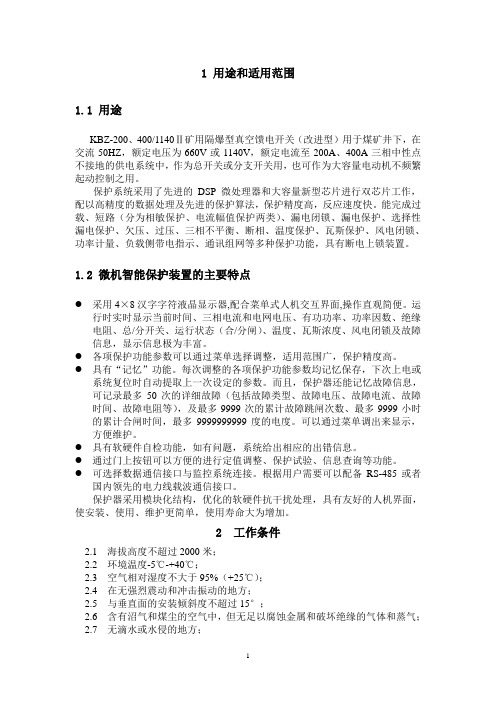
1 用途和适用范围1.1 用途KBZ-200、400/1140Ⅱ矿用隔爆型真空馈电开关(改进型)用于煤矿井下,在交流50HZ,额定电压为660V或1140V,额定电流至200A、400A三相中性点不接地的供电系统中,作为总开关或分支开关用,也可作为大容量电动机不频繁起动控制之用。
保护系统采用了先进的DSP微处理器和大容量新型芯片进行双芯片工作,配以高精度的数据处理及先进的保护算法,保护精度高,反应速度快。
能完成过载、短路(分为相敏保护、电流幅值保护两类)、漏电闭锁、漏电保护、选择性漏电保护、欠压、过压、三相不平衡、断相、温度保护、瓦斯保护、风电闭锁、功率计量、负载侧带电指示、通讯组网等多种保护功能,具有断电上锁装置。
1.2 微机智能保护装置的主要特点●采用4×8汉字字符液晶显示器,配合菜单式人机交互界面,操作直观简便。
运行时实时显示当前时间、三相电流和电网电压、有功功率、功率因数、绝缘电阻、总/分开关、运行状态(合/分闸)、温度、瓦斯浓度、风电闭锁及故障信息,显示信息极为丰富。
●各项保护功能参数可以通过菜单选择调整,适用范围广,保护精度高。
●具有“记忆”功能。
每次调整的各项保护功能参数均记忆保存,下次上电或系统复位时自动提取上一次设定的参数。
而且,保护器还能记忆故障信息,可记录最多50次的详细故障(包括故障类型、故障电压、故障电流、故障时间、故障电阻等),及最多9999次的累计故障跳闸次数、最多9999小时的累计合闸时间,最多9999999999度的电度。
可以通过菜单调出来显示,方便维护。
●具有软硬件自检功能,如有问题,系统给出相应的出错信息。
●通过门上按钮可以方便的进行定值调整、保护试验、信息查询等功能。
●可选择数据通信接口与监控系统连接。
根据用户需要可以配备RS-485或者国内领先的电力线载波通信接口。
保护器采用模块化结构,优化的软硬件抗干扰处理,具有友好的人机界面,使安装、使用、维护更简单,使用寿命大为增加。
ELM842B中文资料(ELM Technology)中文数据手册「EasyDatasheet - 矽搜」

ELM842B CMOS运算放大器
■电气特性(VDD = 1.5V)
参数 输入偏移电压 输入偏置电流 共模输入电压范围 最大输出电压摆幅 最大输出源电流 开环增益 共模抑制比 电源电压抑制比 目前消费 单位增益带宽 压摆率
符号
条件
Vio
Vout=Vdd/2
Hale Waihona Puke IibVcmrVouts Vid=100mV, RL=200kΩ
1 nA
0.04
2.90 V
2.80
V
45 100
μA
80
dB
85
dB
80
dB
145 280 μA
1
MHz
0.45 1.00
V/μs
■标识
SOT-25
No.
Mark
a
C
b
0 to 9
c
0 to 9
内容
ELM842B
批号 批号
芯片中文手册,看全文,戳
ELM842B CMOS运算放大器
ELM842B CMOS运算放大器
■典型特征
源电流 - Vdd
200 180 160 140 120 100
电流8(0 A)
60 40 20
0 123456
Vdd (V) 源电流 - 热门
200
150
100
电流(A)
50
Vdd=3V Vdd=1.5V
-20 -10 0
200 180 160 140 120 100
■Note
1)负载电阻 ELM842B是专为低功耗应用;因此,输出源电流仅为90μA(典型值在VDD = 1.5V).其结果是, ELM842B不能试图驾驶小负载电阻时,以防护持输出电压摆幅.考虑到这一点,负载和反馈电阻为 ELM842B应仔细选择.
富士FUJI 标准IGBT(1MBI、2MBI、6MBI),智能IPM(6MBP、7MBP、7MBR)
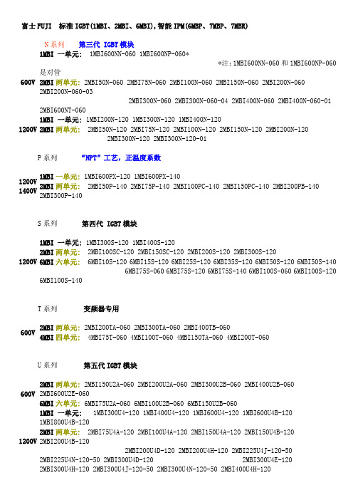
富士FUJI 标准IGBT(1MBI、2MBI、6MBI),智能IPM(6MBP、7MBP、7MBR) N系列第三代 IGBT模块600V 1MBI 一单元: 1MBI600NN-060 1MBI600NP-060**注:1MBI600NN-060和1MBI600NP-060是对管2MBI两单元: 2MBI50N-060 2MBI75N-060 2MBI100N-060 2MBI150N-060 2MBI200N-0602MBI200N-060-032MBI300N-060 2MBI300N-060-04 2MBI400N-060 2MBI400N-060-01 2MBI600NT-0601200V 1MBI 一单元: 1MBI200N-120 1MBI300N-120 1MBI400N-1202MBI两单元: 2MBI50N-120 2MBI75N-120 2MBI100N-120 2MBI150N-120 2MBI200N-120 2MBI300N-120 2MBI300N-120-01P系列“NPT”工艺,正温度系数1200V 1400V 1MBI一单元: 1MBI600PX-120 1MBI600PX-1402MBI两单元: 2MBI50P-140 2MBI75P-140 2MBI100PC-140 2MBI150PC-140 2MBI200PB-140 2MBI300P-140S系列第四代 IGBT模块1200V 1MBI 一单元: 1MBI300S-120 1MBI400S-1202MBI两单元: 2MBI100SC-120 2MBI150SC-120 2MBI200S-120 2MBI300S-1206MBI六单元: 6MBI10S-120 6MBI15S-120 6MBI25S-120 6MBI35S-120 6MBI50S-120 6MBI50S-140 6MBI75S-060 6MBI75S-120 6MBI75S-140 6MBI100S-060 6MBI100S-1206MBI100S-140T系列变频器专用600V 2MBI两单元: 2MBI200TA-060 2MBI300TA-060 2MBI400TB-0604MBI四单元: 4MBI75T-060 4MBI100T-060 4MBI150TA-060 4MBI200T-060U系列第五代IGBT模块600V 2MBI两单元: 2MBI150U2A-060 2MBI200U2A-060 2MBI300U2B-060 2MBI400U2B-060 2MBI600U2E-0606MBI六单元: 6MBI75U2A-060 6MBI100U2B-060 6MBI150U2B-0601200V 1MBI 一单元: 1MBI300U4-120 1MBI400U4-120 1MBI600U4-120 1MBI600U4B-120 1MBI800U4B-120 2MBI两单元: 2MBI75U4A-120 2MBI100U4A-120 2MBI150U4A-120 2MBI150U4B-120 2MBI200U4B-120 2MBI200U4D-120 2MBI200U4H-120 2MBI225U4J-120-50 2MBI225U4N-120-502MBI300U4D-120 2MBI300U4E-120 2MBI300U4H-120 2MBI300U4J-120-502MBI300U4N-120-50 2MBI400U4H-1202MBI450U4E-120 2MBI450U4J-120-50 2MBI450U4N-120-506MBI六单元: 6MBI35U4A-120 6MBI50U4A-120 6MBI75U4A-120 6MBI75U4B-1206MBI75UC-120 6MBI100U4B-120 6MBI100UC-120 6MBI150U4B-120 6MBI225U4-120 6MBI300U4-1206MBI450U4-1201700V 2MBI两单元: 2MBI100U4H-170 2MBI150U4H-170 2MBI200U4H-170 2MBI300U4H-1702MBI400U4H-1706MBI六单元: 6MBI75U4B-170 6MBI100U4B-170 6MBI150U4B-170 6MBI225U4-170 6MBI300U4-170 6MBI450U4-170大电流等级1200V1MBI 一单元: 1MBI1200U4C-120 1MBI1600U4C-120 1MBI2400U4D-120 1MBI3600U4D-120 2MBI两单元: 2MBI600U4G-120 2MBI800U4G-120 2MBI1200U4G-1201700V1MBI 一单元: 1MBI1200U4C-170 1MBI1600U4C-170 1MBI2400U4D-170 1MBI3600U4D-170 2MBI两单元: 2MBI600U4G-170 2MBI800U4G-170 2MBI1200U4G-170智能IGBT模块(IPM)一、工业级IPM:适用于变频空调,伺服控制等,内设欠压、过热、过流保护功能,开关频率最大20kHZ600V电压6MBP六单元:6MBP15RH060 6MBP20RH060 6MBP30RH060二、R系列IPM:(适用于通用变频器等,内设欠压、过热、过流保护功能)600V 电压6MBP六单元:6MBP20RTA060 6MBP50RA060 6MBP75RA060 6MBP100RA060 6MBP150RA060 6MBP200RA060 6MBP300RA060 6MBP50RTB060 6MBP50RTJ060 6MBP75RTB0606MBP75RTJ060 6MBP100RTB060 6MBP100RTJ060 6MBP150RTB060 6MBP150RTJ060 7MBP 七单元:7MBP50RA060 7MBP75RA060 7MBP100RA060 7MBP150RA060 7MBP200RA060 7MBP300RA060 7MBP50RTB060 7MBP50RTJ060 7MBP75RTB060 7MBP75RTJ0607MBP100RTB060 7MBP100RTJ060 7MBP150RTB060 7MBP150RTJ0601200V 电压6MBP六单元: 6MBP15RA120 6MBP25RA120 6MBP50RA120 6MBP50RJ120 6MBP75RA120 6MBP75RJ120 6MBP100RA120 6MBP150RA1207MBP 七单元:7MBP25RA120 7MBP25RJ120 7MBP50RA120 7MBP50RJ1207MBP75RA120 7MBP75RJ120 7MBP100RA120 7MBP150RA120PIM(智能功率集成模块)含整流桥七单元600V电压7MBR20SC060 7MBR30SA060 7MBR30SC060 7MBR50SA060 7MBR50SB060 7MBR50SC060 7MBR75SB060 7MBR75SD060 7MBR100SB060 7MBR100SD0601200V电压7MBR10SA120 7MBR10SC120 7MBR15SA120 7MBR15SC120 7MBR25SA120 7MBR25SC120 7MBR35SB120 7MBR35SD120 7MBR50SB120 7MBR50SD1201400V电压7MBR10SA140 7MBR15SA140 7MBR25SA140 7MBR35SB140 7MBR50SB140。
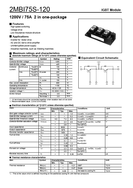
2MBI75S-120中文资料
Err
0
1
10
100
500
Gate resistance : Rg [ohm]
Collector current : Ic [ A ]
Switching loss : Eon, Eoff, Err [ mJ/pulse ]
ton tr
tf 100
50
0
20
40
60
80
100
120
Collector current : Ic [ A ]
Switching loss vs. Collector current (typ.) Vcc=600V, VGE=±15V, Rg=16ohm
20
Eon(125°C)
15
Eon(25°C)
10 Eoff(125°C)
Eoff(25°C)
5
Err(125°C)
Err(25°C)
0
0
20
40
60
80 100 120 140
IGBT Module
180 160 140 120 100
80 60 40 20
0 0
Collector current vs. Collector-Emiiter voltage Tj= 125°C (typ.) VGE= 20V15V 12V
10V
8V
1
2
3
4
5
Collector - Emitter voltage : VCE [ V ]
Equivalent Circuit Schematic
C2E1
C1
E2
G1
E1
G2
E2
Electrical characteristics (at Tj=25°C unless otherwise specified)
2MBI150U2A-060 IGBT模块

Maximum ratings and characteristics
Absolute maximum ratings (at Tc=25°C unless otherwise specified)
Item
Symbol
Conditions
Collector-Emitter voltage
VCES
Gate-Emitter voltage Collector current
15
300
10
5
0 1.0
Eoff Eon Err
10.0 Gate resistance : Rg [ Ω ]
200
100
ห้องสมุดไป่ตู้
100.0
0
0
200
400
600
800
Collector - Emitter voltage : VCE [ V ]
Switching loss : Eon, Eoff, Err [ mJ/pulse ]
Collector-Emitter voltage : VCE [ 200V/div ] Gate - Emitter voltage : VGE [ 5V/div ]
Capacitance : Cies, Coes, Cres [ nF ]
Cies 10.0
Cres
1.0
Coes
0.1 0
10
20
2MBI150U2A-060
Characteristics (Representative)
Collector current vs. Collector-Emitter voltage (typ.) Tj= 25°C / chip
富士和英飞凌IGBT模块型号互换对照表
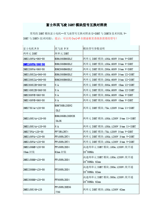
2MBI200HH-120-50
FF200R12KS4
高速两单元IGBT模块;200A;1200V;软开通20~50KHz 62mm
2MBI300HH-120-50
FF300R12KS4
高速两单元IGBT模块;300A;1200V;软开通20~50KHz 62mm
IGBT功率集成模块(PIM);50A;1200V EconoPIM 3
7MBR75VB120-50
FP75R12KT4_B15
IGBT功率集成模块(PIM);75A;1200V EconoPIM 3
7MBR75VN120-50
FP75R12KT4
IGBT功率集成模块(PIM);75A;1200V EconoPIM 3
6MBI150VB-120
FS150R12KT4
六单元IGBT模块;150A;1200V EconoPACK 3
6MBI300V-120
FS300R12KE3/E4
六单元IGBT模块;300A;1200V EconoPACK +
6MBI450V-120
FS450R12KE3/E4
六单元IGBT模块;450A;1200V EconoPACK +
7MBR100VN120-50
FP100R12KT4
IGBT功率集成模块(PIM);100A;1200V EconoPIM 3
7MBR150VN120-50
FP150R12KT4
IGBT功率集成模块(PIM);150A;1200V EconoPIM 3
1单元模块
1MBI2400VC-120
FZ2400R12KE3
2MBI200N-060
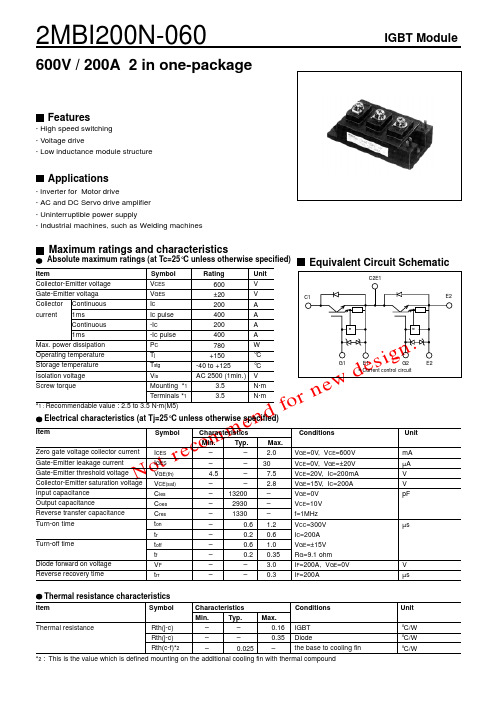
Not r ec o m m e ndf or2MBI200N-060IGBT Module600V / 200A 2 in one-packageFeatures· High speed switching · Voltage drive· Low inductance module structureApplications· Inverter for Motor drive· AC and DC Servo drive amplifier· Uninterruptible power supply· Industrial machines, such as Welding machinesMaximum ratings and characteristicsAbsolute maximum ratings (at Tc=25°C unless otherwise specified)Item Symbol Collector-Emitter voltage V CES Gate-Emitter voltaga V GES Collector Continuous I C current 1ms I C pulseContinuous -I C 1ms -I C pulseMax. power dissipation P C Operating temperature T j Storage temperature T stg Isolation voltage V is Screw torque Mounting *1Terminals *1 Rating600±20200400200400780+150-40 to +125AC 2500 (1min.)3.53.5Unit V V A A A A W °C °C V N·m N·mItemZero gate voltage collector current Gate-Emitter leakage current Gate-Emitter threshold voltageCollector-Emitter saturation voltage Input capacitance Output capacitanceReverse transfer capacitance Turn-on time Turn-off timeDiode forward on voltage Reverse recovery timeI CES I GES V GE(th)V CE(sat)C ies C oes C res t on t r t off t f V F t rr –– 2.0––304.5–7.5–– 2.8–13200––2930––1330––0.6 1.2–0.20.6–0.6 1.0–0.20.35–– 3.0––0.3V GE =0V, V CE =600V V CE =0V, V GE =±20V V CE =20V, I C =200mA V GE =15V, I C =200A V GE =0V V CE =10V f=1MHz V CC =300V I C =200A V GE =±15V R G =9.1 ohm I F =200A, V GE =0V I F =200A mA µA V V pF µs V µsElectrical characteristics (at Tj=25°C unless otherwise specified)Thermal resistance characteristicsThermal resistance ––0.16––0.35–0.025 –IGBT Diode the base to cooling fin °C/W°C/W °C/W *2 : This is the value which is defined mounting on the additional cooling fin with thermal compoundEquivalent Circuit Schematic*1 : Recommendable value : 2.5 to 3.5 N·m(M5)Symbol Characteristics Conditions UnitMin. Typ. Max.Item Symbol Characteristics Conditions UnitMin. Typ. Max.Rth(j-c)Rth(j-c)Rth(c-f)*2Not r ec o m m e ndf or n ew de s i g n .Characteristics (Representative)Collector current vs. Collector-Emitter voltage Tj=25°CCollector current vs. Collector-Emitter voltage Tj=125°CCollector-Emitter vs. Gate-Emitter voltage Tj=25°C Collector-Emitter vs. Gate-Emitter voltage Tj=125°CSwitching time vs. Collector currentVcc=300V, R G =9.1 ohm, V GE =±15V, Tj=25°C Switching time vs. Collector currentVcc=300V, R G =9.1 ohm, V GE =±15V, Tj=125°CCollector-Emitter voltage : V CE [V]Collector-Emitter voltage : V CE [V]C o l l e c t o r c u r r e n t : I c [A ]C o l l e c t o r c u r r e n t : I c [A ]400300200100 00 1 2 3 4 50 1 2 3 4 5C o l l e c t o r -E m i t t e r v o l t a g e : V C E [V ]C o l l e c t o r -E m i t t e r v o l t a g e : V C E [V ]0 5 10 15 20 250 5 10 15 20 25108642 0Gate-Emitter voltage : V GE [V]Gate-Emitter voltage : V GE [V]S w i t c h i n g t i m e : t o n , t r , t o f f , t f [n s e c .]100010010Collector current : Ic [A]Collector current : Ic [A]S w i t c h i n g t i m e : t o n , t r , t o f f , t f [n s e c .]10001001010 8 6 420 50 100 150 200 250 3004003002001000 50 100 150 200 250 300N ot rec o m m e nd f or n ew de s i g n . Switching time vs. RGVcc=300V, Ic=200A, V GE =±15V, Tj=25°CDynamic input characteristicsTj=25°CGate resistance : R G [ohm]5 10Gate charge : Qg [nC]1001000100S w i t c h i n g t i m e : t o n , t r , t o f f , t f [n s e c .]C o l l e c t o r -E m i t t e r v o l t a g e : V C E [V ]C o l l e c t o r c u r r e n t : -I c [A ](F o r w a r d c u r r e n t : I F [A ] )5004003002001000 1 2 3 4G a t e -E m i t t e r v o l t a g e : V G E [V ]Emitter-Collector voltage V ECD [V](Forward voltage : V F [V])R e v e r s e r e c o v e r y c u r r e n t : I r r [A ]R e v e r s e r e c o v e r y t i m e : t r r [n s e c .]Forward current vs. Forward voltage V GE =0VReverse recovery characteristics trr, Irr, vs. IFForward current : I F [A]1005020151050 100 200 300200018001600140012001000 800 600 400 2000 100 200 300 400 500 600Collector-Emitter voltage : V CE [V]C o l l e c t o r c u r r e n t : I c [A ]10Collector current : Ic [A]S w i t c h i n g l o s s : E o n , E o f f , E r r [m J /c y c l e ]Switching loss vs. Collector currentVcc=300V, R G =9.1 ohm, V GE =±15VReversed biased safe operating area+V GE =15V, -V GE = 15V, Tj = 125°C, R G = 9.1 ohm<<>25201510500 100 200 300500400300200100 00 200 400 600 800 1000 1200Not r ec o m m e ndf or n ew de s i g n .Outline Drawings, mm0.010.001 0.01 0.1 1Collector-Emitter voltage : V CE [V]110C a p a c i t a n c e : C i e s , C o e s , C r e s [n F ]Capacitance vs. Collector-Emitter voltage Tj=25°Cmass : 240g0.1Pulse width : P W [sec.]T h e r m a l r e s i s t a nce : R t h (j -c ) [°C /W ]Transient thermal resistance0 5 10 15 20 25 30 35。
CM400DY-24A中文资料
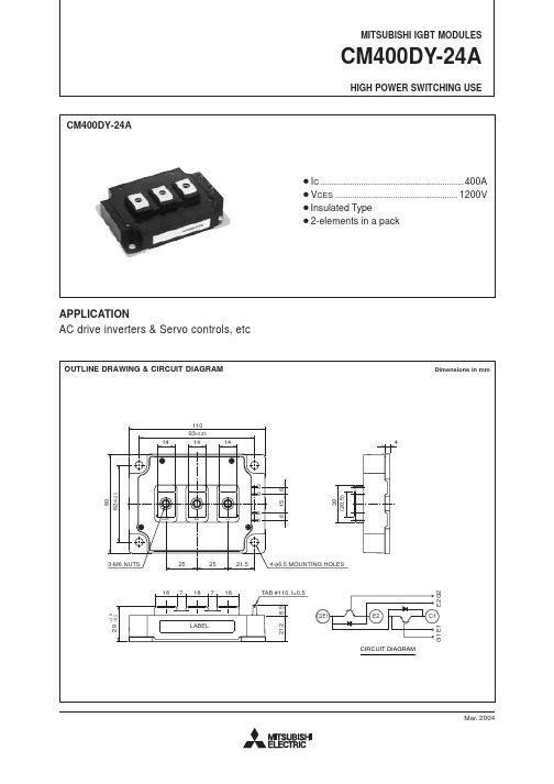
V CE = V CES , V GE = 0V V GE = V GES , V CE = 0V T j = 25°CT j = 125°C V CC = 600V, I C = 400A, V GE = 15VV CC = 600V, I C = 400A V GE1 = V GE2 = 15VR G = 0.78Ω, Inductive load switching operation I E = 400AI E = 400A, V GE = 0V IGBT part (1/2 module)*1FWDi part (1/2 module)*1Case to fin, Thermal compound Applied (1/2 module)*2I C = 40mA, V CE = 10VI C = 400A, V GE = 15VV CE = 10V V GE = 0V1200±204008004008002710–40 ~ +150–40 ~ +12525003.5 ~ 4.53.5 ~ 4.5580HIGH POWER SWITCHING USEV V A A W °C °C V N • m g10.53.0—7061.4—550180600350250—3.80.0460.085—10mA µA nF nC ns µC V °C/W Ω——2.12.4———2000—————16———0.02———————————————————0.787V V 68ns I CES I GES C ies C oes C res Q G t d(on)t rt d(off)t ft rr (Note 1)Q rr (Note 1)V EC(Note 1)R th(j-c)Q R th(j-c)R R th(c-f)R GSymbol ParameterV GE(th)V CE(sat)*1 : Tc, Tf measured point is just under the chips.*2 : Typical value is measured by using Shin-etsu Silicone “G-746”.Note 1. I E , V EC , t rr & Q rr represent characteristics of the anti-parallel, emitter to collector free-wheel diode (FWDi).2. Pulse width and repetition rate should be such that the device junction temp. (T j ) does not exceed T jmax rating.3. Junction temperature (T j ) should not increase beyond 150°C.Collector-emitter voltage Gate-emitter voltage Maximum collector dissipation Junction temperature Storage temperature Isolation voltage WeightG-E Short C-E ShortDC, T C = 85°C *1Pulse (Note 2)Pulse(Note 2)T C = 25°C *1Main terminal to base plate, AC 1 min.Main terminal M6Mounting holes M6Typical valueSymbol ParameterCollector current Emitter currentTorque strength ConditionsUnit Ratings V CES V GES I C I CMI E (Note 1)I EM (Note 1)P C (Note 3)T j T stg V iso———Unit Typ.Limits Min.Max.Test conditionsELECTRICAL CHARACTERISTICS (Tj = 25°C)ABSOLUTE MAXIMUM RATINGS (Tj = 25°C)Collector cutoff current Gate-emitter threshold voltageGate leakage currentCollector-emitter saturation voltageInput capacitance Output capacitanceReverse transfer capacitance Total gate charge Turn-on delay time Turn-on rise time Turn-off delay time Turn-off fall timeReverse recovery time Reverse recovery charge Emitter-collector voltage Contact thermal resistance External gate resistanceThermal resistanceHIGH POWER SWITCHING USEHIGH POWER SWITCHING USEHIGH POWER SWITCHING USE。
2MBI200U4B-120中文资料

Contact Thermal resistance Rth(c-f) with Thermal Compound 0.025 (1 device) (*4) (*4) This is the value which is defined mounting on the additional cooling fin with thermal compound.
(Aug.-2001 edition)
Mechanical Tests
Test Method 401 MethodⅠ Test Method 402 methodⅡ Test Method 403 Reference 1 Condition code B
3 Vibration
4 Shock
1 High Temperature Storage 2 Low Temperature Storage 3 Temperature Humidity Storage 4 Unsaturated Pressurized Vapor
C/W
6. Indication on module Logo of production
2MBI200U4B-120
200A 1200V
Lot.No. 7. Applicable category
Place of manufacturing (code)
This specification is applied to IGBT-Module named 2MBI200U4B-120.
MS5F6032
5 13
H04-004-03a
元器件交易网
11. Reliability test results
Reliability Test Items
2MBI100N-120中文资料
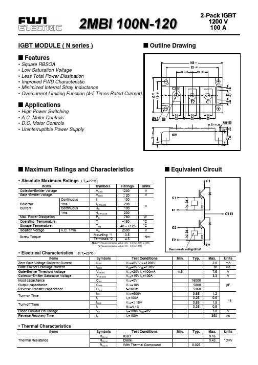
• Absolute Maximum Ratings ( Tc=25°C)
Items
Symbols
Ratings Units
Collector-Emitter Voltage Gate -Emitter Voltage
VCES VGES
1200
V
± 20
V
Collector Current
Max. Power Dissipation Operating Temperature Storage Temperature
Items
Symbols
Zero Gate Voltage Collector Current
ICES
Gate-Emitter Leackage Current
IGES
Gate-Emitter Threshold Voltage
VGE(th)
Collector-Emitter Saturation Voltage
Continuous 1ms Continuous 1ms
IC IC PULSE -IC -IC PULSE PC Tj Tstg
100
200
A
100
200
780
W
+150
°C
-40 ∼ +125 °C
Isolation Voltage Screw Torque
A.C. 1min.
Vis
2500
V
Mounting *1
trr
Test Conditions VGE=0V VCE=1200V VCE=0V VGE=± 20V VGE=20V IC=100mA VGE=15V IC=100A VGE=0V VCE=10V f=1MHz VCC=600V IC=100A VGE=± 15V RG=9.1Ω IF=100A VGE=0V IF=100A
WT-2000系列中文手册

电话: +86-10-65863598
传真: +86-10-65863018
瑟米莱伯公司无锡售后服务中心
电话: +86-13812056089
警告:WT-2000PV系列激光探头安全等级为1M级,操作时必须佩戴防护眼镜。切勿直视,以及通过镜面和放大镜等光学设备观测激光探头!
在下一个输入框中输入SHR的真实值。
点击OK,取出片子,放入另一片子,接着重复上面的步骤,校正数据被保存。
最后点击functions\save ,取文件名,保存较正文件。
2.4 Fe
在晶体生长,加工或运输过程中,Fe是一种很容易引起材料沾污的金属,-PCD能够对Fe的沾污量进行定性测试。在p型硅片中,Fe主要以FeB形式存在,若对硅片进行或强光照射,FeB对会分解成Fei,利用FeB和Fei在硅中具有不同的复合强度,通过测试复合前后硅片的少子寿命来计算硅中的Fe沾污浓度。在硅中FeB的少子寿命随注入强度基本不变,而Fei的少子寿命随着注入强度的增大而升高,如图2-4所示。
为测量电池的电流,样品的背面用金属台面连接,正面有个金属探针与主电极接触。LBIC测试原理如图2-2所示:
图2-2 LBIC测试原理示意图
光诱导电流指的是是电池片吸收激光所形成的电流。电池片反射率则是电池片对激光的反射(包括直反射和漫反射)程度,反射率可以通过积分球收集反射信号计算出。
在测得电池片光诱导电流和反射率之后,就能通过计算得出电池片内量子效率(IQE,Internal Quantum Efficiency),其关系如下式所示:
Eddy Current/涡流法体电阻率扫描
Iron concentration/无接触铁含量扫描
XM2400LB-PM0601中文资料
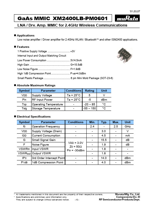
2.5 F (dB) VSWR, F (dB)
VSWR
10 F 5
2.0
1.5
Frequency (GHz)
Input and Output VSWR v.s. Frequency
Gain and F v.s. Frequency
40 20 Output (dBm) 0 -20 -40 -60 -80 -40 Third Order Distortion Fundamental
VSWRin Input VSWR VSWRout Output VSWR IP3 P1dB 3rd Order Intercept Point 1dB Compression Point
C L
RFout RFin
A
Value Part No. C GRM36 5.6pF (Murata) L LQP10 6.8nH (Murata)
1.20 1.20
‘01,03,07
GaAs MMIC XM2400LB-PM0601
LNA / Drv. Amp. MMIC for 2.4GHz Wireless Communications
! Evaluation Board 1 (for High Gain)
VDD
Part No. C1 C1 C2 C2 GRM39 GRM39
! Electrical Specifications Symbol Parameter f0 Operation Frequency VDD IDD G F Supply Voltage (Drain) Current Consumption Small Signal Gain Noise Figure Conditions VDD = 3.0V Z0 = 50Ω Pin = -30dBm Min. 2.4 Typ. 3.0 4.5 15.5 1.9 1.8 1.8 14.0 4.0 Max. 2.5 Unit GHz V mA dB dB dBm dBm
FC21中文资料

Electrical Connection
B E/D S
C
80
G
ID -- VDS
[FET]
80
ID -- VDS
[FET]
Drain Current, ID -- mA
Drain Current, ID -- mA
60
VGS=0
--0.5V
--1.0V
60
VGS=0
--0.5V
40
40
--1.0V
100
ID -- VGS
[FET]
ID -- VGS
[FET]
VDS=10V
VDS=10V IDSS=60mA
Drain Current, ID -- mA
100
80
80
60
60
=7
5m
40
40
ID
40 m
20
Ta =
75
SS
55
--2
A
°C
20
0 --6 --5 --4 --3 --2 --1 0 ITR01963 --6 --5 --4 --3 --2 --1
SANYO Electric Co.,Ltd. Semiconductor Company
TOKYO OFFICE Tokyo Bldg., 1-10, 1 Chome, Ueno, Taito-ku, TOKYO, 110-8534 JAPAN
81001 TS IM TA-1526 No.7021-1/5
Parameter [FET] Drain-to-Source Voltage Gate-to-Drain Voltage Gate Current Drain Current Allowable Power Dissipation [TR] Collector-to-Base Voltage Collector-to-Emitter Voltage Emitter-to-Base Voltage Collector Current Collector Current(Pulse) Base Current Collector Dissipation [Common Ratings] Total Dissipation Junction Temperature Storage Temperature PT Tj Tstg 600 150 --55 to +150 mW °C °C VCBO VCEO VEBO IC ICP IB PC 55 50 6 150 300 30 200 V V V mA mA mA mW VDSX VGDS IG ID PD 40 -40 10 75 400 V V mA mA mW Symbol Conditions Ratings Unit
富士IGBT模板各类型号统参数统计
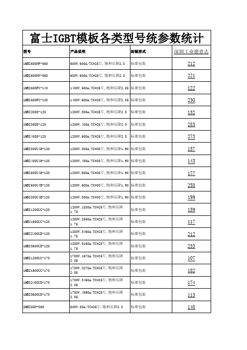
274
2MBI100PC-140
1400V,100A/TC=25℃,饱和压降2.7 标准包装
139
2MBI150PC-140
1400V,150A/TC=25℃,饱和压降2.7 标准包装
190
2MBI200PB-140
1400V,200A/TC=25℃,饱和压降2.7 标准包装
183
2MBI300P-140
1200V,300A/TC=25℃,饱和压降2.3 标准包装
131
2MBI300S-120
1200V,400A/TC=25℃,饱和压降2.3 标准包装
174
2MBI75U4A-120
1200V,75A/TC=80℃,饱和压降1.9 标准包装
134
2MBI100U4A-120
1200V,100A/TC=80℃,饱和压降1.9 标准包装
277
6MBI75S-120
1200V,100A/TC=25℃,饱和压降2.3 标准包装
230
6MBI100S-120
1200V,150A/TC=25℃,饱和压降2.3 标准包装
185
6MBI50U4A-120
1200V,50A/Tc=80℃,饱和压降1.9 标准包装
134
6MBI75U4A-120
1200V,200A/TC=80℃,饱和压降1.9 标准包装
256
2MBI200U4H-120
1200V,200A/TC=80℃,饱和压降1.9 标准0A/TC=80℃,饱和压降1.9 标准包装
223
2MBI300U4H-120
1200V,300A/TC=80℃,饱和压降1.9 标准包装
1400V,300A/TC=25℃,饱和压降2.7 标准包装
变频器滤波器的作用
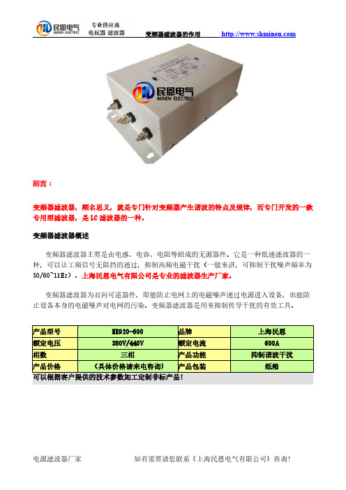
前言:变频器滤波器,顾名思义,就是专门针对变频器产生谐波的特点及规律,而专门开发的一款专用型滤波器,是LC滤波器的一种。
变频器滤波器概述变频器滤波器主要是由电感、电容、电阻等组成的无源器件。
它是一种低通滤波器的一种,可以让工频信号无阻挡的通过,抑制高频电磁干扰(一般来讲,可抑制干扰噪声频率为50/60~1kHz)。
上海民恩电气有限公司是专业的滤波器生产厂家。
变频器滤波器为双向可逆器件,即能防止电网上的电磁噪声通过电源进入设备,也能防止设备本身的电磁噪声对电网的污染。
变频器滤波器是用来抑制传导干扰的有效工具。
产品型号ME920-600品牌上海民恩额定电压380V/440V额定电流600A相数三相产品功能抑制谐波干扰产品价格(具体价格请来电咨询)产品包装纸箱可以根据客户提供的技术参数加工定制非标产品!制造商Manufacturer上海民恩电气有限公司依据标准Standard GB/T7343-87《10kHz-30MHz无源无线电干扰滤波器和抑制元件抑制特性的测量方法》及UL1283《电磁干扰滤波器》标准制定型式Type输入滤波器防护等级Protection level IP20配套变频器功率45KW额定电流Se.Cur100A系统电压Se.Vol0.4KV连接方式Connection mode串联相数Number of phases三相工作频率Frequency50/60Hz气候类别Climate category25/085/21泄露电流(250VAC/50Hz)<50mA冷却方式Cooling Type自冷试验电压(线-线)2250VDC极壳耐压Extreme pressure3000Vac/1min试验电压(线-地)2700VDC过载电流Overload current开机瞬间允许通过4倍过工作电流,1.4倍工作电流1分钟(每小时一次)包装Packing纸箱运输方式Transport快递运输质保期Warranty period一年产品货期Delivery2-3天公司网站:一、变频器滤波器的作用原理图二、变频器滤波器的作用型号含义ME920-100额定电流100A输入滤波器代码民恩公司型号标示三、变频器滤波器的作用波形图四、变频器滤波器的作用谐波示意图五、变频器滤波器的作用变频器干扰范围图示六、变频器滤波器的作用安装接线图安装位置示意图七、变频器滤波器的作用安装使用说明安装使用注意事项滤波器安装前请先阅读此注意事项!!!1.测试上海民恩电气有限公司的每一只产品在出厂前均经过严格的测试,但为出于安全考虑,建议您最好在使用前对“试验电压”进行测试;2.接地滤波器在加电使用前必须保证安全地线的连接(具体连接方法参照安装操作步骤说明的第二步),否则会造成人身伤害或财产损失;3.面接触滤波器底面为金属表面,为保证滤波器的滤波效果,请尽可能的将其面接触于金属支架或机柜表面(之间无任何绝缘物质);4.安装位置滤波器的安装应尽量靠近变频器侧,通常情况下滤波器与变频器之间的连线越短越好,不宜超过1米;5.布线滤波器的输入线与输出线不得平行或交叉;应使输入、输出线尽量远离;6.检查每年应最少一次对滤波器的连接进行检查。
AM29F040B-1资料

This Data Sheet states AMD’s current technical specifications regarding the Products described herein. This Data Sheet may be revised by subsequent versions or modifications due to changes in technical specifications.Publication# 21445Rev: E Amendment/0 Issue Date: November 29, 2000Am29F040B4 Megabit (512 K x 8-Bit)CMOS 5.0 Volt-only, Uniform Sector Flash Memory DISTINCTIVE CHARACTERISTICSs 5.0 V ± 10% for read and write operations —Minimizes system level power requirementss Manufactured on 0.32µm process technology —Compatible with 0.5 µm Am29F040 devices High performance—Access times as fast as 55 nss Low power consumption—20 mA typical active read current—30 mA typical program/erase current—1 µA typical standby current (standard access time to active mode)s Flexible sector architecture—8 uniform sectors of 64 Kbytes each—Any combination of sectors can be erased—Supports full chip erase—Sector protection:A hardware method of locking sectors to preventany program or erase operations within that sector s Embedded Algorithms—Embedded Erase algorithm automatically preprograms and erases the entire chip or anycombination of designated sectors—Embedded Program algorithm automatically writes and verifies bytes at specified addresses s Minimum 1,000,000 program/erase cycles per sector guaranteeds20-year data retention at 125°C—Reliable operation for the life of the systems Package options—32-pin PLCC, TSOP, or PDIPs Compatible with JEDEC standards—Pinout and software compatible withsingle-power-supply Flash standard—Superior inadvertent write protections Data# Polling and toggle bits—Provides a software method of detecting program or erase cycle completions Erase Suspend/Erase Resume—Suspends a sector erase operation to read data from, or program data to, a non-erasing sector,then resumes the erase operationGENERAL DESCRIPTIONThe Am29F040B is a 4 Mbit, 5.0 volt-only Flash mem-ory organized as 524,288 Kbytes of 8 bits each. The 512 Kbytes of data are divided into eight sectors of 64 Kbytes each for flexible erase capability. The 8 bits of data appear on DQ0–DQ7. The Am29F040B is offered in 32-pin PLCC, TSOP, and PDIP packages. This device is designed to be programmed in-system with the stan-dard system 5.0 volt V CC supply. A 12.0 volt V PP is not required for write or erase operations. The device can also be programmed in standard EPROM programmers. This device is manufactured using AMD’s 0.32 µm pro-cess technology, and offers all the features and benefits of the Am29F040, which was manufactured using 0.5 µm process technology. In addtion, the Am29F040B has a second toggle bit, DQ2, and also of-fers the ability to program in the Erase Suspend mode. The standard Am29F040B offers access times of 55, 70, 90, 120, and 150 ns, allowing high-speed micropro-cessors to operate without wait states. To eliminate bus contention the device has separate chip enable (CE#), write enable (WE#) and output enable (OE#) controls. The device requires only a single 5.0 volt power sup-ply for both read and write functions. Internally generated and regulated voltages are provided for the program and erase operations.The device is entirely command set compatible with the JEDEC single-power-supply Flash standard. Com-mands are written to the command register using standard microprocessor write timings. Register con-tents serve as input to an internal state-machine that controls the erase and programming circuitry. Write cy-cles also internally latch addresses and data needed for the programming and erase operations. Reading data out of the device is similar to reading from other Flash or EPROM devices.Device programming occurs by executing the program command sequence. This initiates the Embedded Program algorithm—an internal algorithm that auto-matically times the program pulse widths and verifies proper cell margin.Device erasure occurs by executing the erase com-mand sequence. This initiates the Embedded Erase algorithm—an internal algorithm that automatically preprograms the array (if it is not already programmed) before executing the erase operation. During erase, the device automatically times the erase pulse widths and verifies proper cell margin.The host system can detect whether a program or erase operation is complete by reading the DQ7 (Data# Polling) and DQ6 (toggle) status bits. After a program or erase cycle has been completed, the device is ready to read array data or accept another command.The sector erase architecture allows memory sectors to be erased and reprogrammed without affecting the data contents of other sectors. The device is fully erased when shipped from the factory.Hardware data protection measures include a low V CC detector that automatically inhibits write opera-tions during power transitions. The hardware sector protection feature disables both program and erase operations in any combination of the sectors of mem-ory. This can be achieved via programming equipment. The Erase Suspend feature enables the user to put erase on hold for any period of time to read data from, or program data to, any sector that is not selected for erasure. True background erase can thus be achieved. The system can place the device into the standby mode. Power consumption is greatly reduced in this mode. AMD’s Flash technology combines years of Flash memory manufacturing experience to produce the highest levels of quality, reliability and cost effective-ness. The device electrically erases all bits within a sector simultaneously via Fowler-Nordheim tunneling. The data is programmed using hot electron injection.2Am29F040BTABLE OF CONTENTSProduct Selector Guide. . . . . . . . . . . . . . . . . . . . . 4 Block Diagram . . . . . . . . . . . . . . . . . . . . . . . . . . . . 4 Connection Diagrams . . . . . . . . . . . . . . . . . . . . . . 5 Pin Configuration. . . . . . . . . . . . . . . . . . . . . . . . . . 6 Logic Symbol. . . . . . . . . . . . . . . . . . . . . . . . . . . . . 6 Ordering Information. . . . . . . . . . . . . . . . . . . . . . . 7 Device Bus Operations . . . . . . . . . . . . . . . . . . . . . 8 Table 1. Am29F040B Device Bus Operations (8)Requirements for Reading Array Data (8)Writing Commands/Command Sequences (8)Program and Erase Operation Status (8)Standby Mode (8)Output Disable Mode (9)Table 2. Sector Addresses Table (9)Autoselect Mode (10)Table 3. Am29F040B Autoselect Codes (High Voltage Method) (10)Sector Protection/Unprotection (10)Hardware Data Protection (10)Low V CC Write Inhibit (10)Write Pulse “Glitch” Protection (10)Logical Inhibit (10)Power-Up Write Inhibit (10)Command Definitions . . . . . . . . . . . . . . . . . . . . . 11 Reading Array Data (11)Reset Command (11)Autoselect Command Sequence (11)Byte Program Command Sequence (11)Figure 1. Program Operation (12)Chip Erase Command Sequence (12)Sector Erase Command Sequence (12)Erase Suspend/Erase Resume Commands (13)Figure 2. Erase Operation (13)Command Definitions (14)Table 4. Am29F040B Command Definitions (14)Write Operation Status . . . . . . . . . . . . . . . . . . . . 15 DQ7: Data# Polling (15)Figure 3. Data# Polling Algorithm (15)DQ6: Toggle Bit I (16)DQ2: Toggle Bit II (16)Reading Toggle Bits DQ6/DQ2 (16)DQ5: Exceeded Timing Limits (16)DQ3: Sector Erase Timer (17)Figure 4. Toggle Bit Algorithm (17)Table 5. Write Operation Status.......................................................18Absolute Maximum Ratings. . . . . . . . . . . . . . . . . 19 Figure 5. Maximum Negative Overshoot Waveform (19)Figure 6. Maximum Positive Overshoot Waveform (19)Operating Ranges. . . . . . . . . . . . . . . . . . . . . . . . . 19 DC Characteristics . . . . . . . . . . . . . . . . . . . . . . . . 20 TTL/NMOS Compatible (20)CMOS Compatible (20)Test Conditions. . . . . . . . . . . . . . . . . . . . . . . . . . . 21 Figure 7. Test Setup (21)Table 6. Test Specifications (21)Key to Switching Waveforms. . . . . . . . . . . . . . . . 21 AC Characteristics . . . . . . . . . . . . . . . . . . . . . . . . 22 Read Only Operations (22)Figure 8. Read Operation Timings (22)Erase and Program Operations (23)Figure 9. Program Operation Timings (24)Figure 10. Chip/Sector Erase Operation Timings (24)Figure 11. Data# Polling Timings (During Embedded Algorithms) 25 Figure 12. Toggle Bit Timings (During Embedded Algorithms) (25)Figure 13. DQ2 vs. DQ6 (26)AC Characteristics . . . . . . . . . . . . . . . . . . . . . . . . 27 Erase and Program Operations (27)Alternate CE# Controlled Writes (27)Figure 14. Alternate CE# Controlled Write Operation Timings (28)Erase and Programming Performance. . . . . . . . 29 Latchup Characteristics. . . . . . . . . . . . . . . . . . . . 29 TSOP Pin Capacitance . . . . . . . . . . . . . . . . . . . . 29 PLCC and PDIP Pin Capacitance. . . . . . . . . . . . . 30 Data Retention. . . . . . . . . . . . . . . . . . . . . . . . . . . . 30 Physical Dimensions . . . . . . . . . . . . . . . . . . . . . . 31 PD 032—32-Pin Plastic DIP (31)PL 032—32-Pin Plastic Leaded Chip Carrier (32)TS 032—32-Pin Standard Thin Small Package (33)TSR032—32-Pin Reversed Thin Small Outline Package (34)Revision Summary . . . . . . . . . . . . . . . . . . . . . . . . 35 Revision A (May 1997) (35)Revision B (January 1998) (35)Revision B+1 (January 1998) (35)Revision B+2 (April 1998) (35)Revision C (January 1999) (35)Revision C+1 (February 1999) (35)Revision C+2 (May 17, 1999) (35)Revision D (November 15, 1999) (35)Revision E (November 29, 2000) (35)Am29F040B34Am29F040BPRODUCT SELECTOR GUIDENote: See the “AC Characteristics” section for more information.BLOCK DIAGRAMFamily Part Number Am29F040BSpeed OptionV CC = 5.0 V ± 5%-55V CC = 5.0 V ± 10%-70-90-120-150Max access time, ns (t ACC )557090120150Max CE# access time, ns (t CE )557090120150Max OE# access time, ns (t OE )2530355055Erase Voltage GeneratorY -GatingCell MatrixX-Decoder Y -Decoder A d d r e s s L a t c hChip Enable Output EnableLogicPGM Voltage GeneratorTimerV CC DetectorState Control Command RegisterWE#CE#OE#A0–A18STBSTBDQ0–DQ7V CC V SSData Latch Input/Output BuffersAm29F040B5CONNECTION DIAGRAMSV CCWE#A17A14A13A8A9A11OE#A10CE#DQ7DQ6DQ5DQ4DQ3A18A16A15A12A7A6A5A4A3A2A1A0DQ0DQ1DQ2V SS1234567891011121314151632313029282726252423222120191817PDIPPIN CONFIGURATIONA0–A18=Address InputsDQ0–DQ7=Data Input/OutputCE#=Chip EnableWE#=Write EnableOE#=Output EnableV SS=Device GroundV CC=+5.0 V single power supply(see Product Selector Guide fordevice speed ratings and voltagesupply tolerances)LOGIC SYMBOL198DQ0–DQ7A0–A18CE#OE#WE#6Am29F040BAm29F040B 7ORDERING INFORMATION Standard ProductsAMD standard products are available in several packages and operating ranges. The order number (Valid Combination) is formed by a combination of the following: Valid CombinationsValid Combinations list configurations planned to be sup-ported in volume for this device. Consult the local AMD sales office to confirm availability of specific valid combinations and to check on newly released combinations.Am29F040B-55ECTEMPERATURE RANGE C =Commercial(0°C to +70°C)I = Industrial (–40°C to +85°C)E =Extended (–55°C to +125°C)PACKAGE TYPE P =32-Pin Plastic DIP (PD 032)J =32-Pin Rectangular Plastic Leaded Chip Carrier (PL 032)E =32-Pin Thin Small Outline Package (TSOP) Standard Pinout (TS 032)F =32-Pin Thin Small Outline Package (TSOP) Reverse Pinout (TSR032)SPEED OPTIONSee Product Selector Guide and Valid CombinationsDEVICE NUMBER/DESCRIPTION Am29F040B4 Megabit (512 K x 8-Bit) CMOS 5.0 Volt-only Sector Erase Flash Memory 5.0 V Read, Program, and EraseValid CombinationsV CC Voltage AM29F040B-55JC, JI, JE, EC, EI, EE, FC, FI, FE 5.0 V ± 5%AM29F040B-70 5.0 V ± 10%AM29F040B-90PC, PI, PE, JC, JI, JE, EC, EI, EE,FC, FI, FEAM29F040B-120AM29F040B-150DEVICE BUS OPERATIONSThis section describes the requirements and use of the device bus operations, which are initiated through the internal command register. The command register it-self does not occupy any addressable memory location. The register is composed of latches that store the commands, along with the address and data infor-mation needed to execute the command. The contents of the register serve as inputs to the internal state ma-chine. The state machine outputs dictate the function of the device. The appropriate device bus operations table lists the inputs and control levels required, and the resulting output. The following subsections describe each of these operations in further detail.Table 1.Am29F040B Device Bus OperationsLegend:L = Logic Low = V IL, H = Logic High = V IH, V ID = 12.0 ± 0.5 V, X = Don’t Care, D IN = Data In, D OUT = Data Out, A IN = Address In Note: See the “Sector Protection/Unprotection” section. for more information.Requirements for Reading Array DataTo read array data from the outputs, the system must drive the CE# and OE# pins to V IL. CE# is the power control and selects the device. OE# is the output con-trol and gates array data to the output pins. WE# should remain at V IH.The internal state machine is set for reading array data upon device power-up, or after a hardware reset. This ensures that no spurious alteration of the memory con-tent occurs during the power transition. No command is necessary in this mode to obtain array data. Standard microprocessor read cycles that assert valid addresses on the device address inputs produce valid data on the device data outputs. The device remains enabled for read access until the command register contents are altered.See “Reading Array Data” for more information. Refer to the AC Read Operations table for timing specifica-tions and to the Read Operations Timings diagram for the timing waveforms. I CC1 in the DC Characteristics table represents the active current specification for reading array data.Writing Commands/Command Sequences To write a command or command sequence (which in-cludes programming data to the device and erasing sectors of memory), the system must drive WE# and CE# to V IL, and OE# to V IH.An erase operation can erase one sector, multiple sec-tors, or the entire device. The Sector Address Tables indicate the address space that each sector occupies.A “sector address” consists of the address bits required to uniquely select a sector. See the “Command Defini-tions” section for details on erasing a sector or the entire chip, or suspending/resuming the erase operation.After the system writes the autoselect command se-quence, the device enters the autoselect mode. The system can then read autoselect codes from the inter-nal register (which is separate from the memory array) on DQ7–DQ0. Standard read cycle timings apply in this mode. Refer to the “Autoselect Mode” and “Autoselect Command Sequence” sections for more information.I CC2 in the DC Characteristics table represents the ac-tive current specification for the write mode. The “AC Characteristics” section contains timing specification tables and timing diagrams for write operations.Program and Erase Operation Status During an erase or program operation, the system may check the status of the operation by reading the status bits on DQ7–DQ0. Standard read cycle timings and I CC read specifications apply. Refer to “Write Operation Status” for more information, and to each AC Charac-teristics section for timing diagrams.Standby ModeWhen the system is not reading or writing to the device, it can place the device in the standby mode. In this mode, current consumption is greatly reduced, and theOperation CE#OE#WE#A0–A20DQ0–DQ7 Read L L H A IN D OUT Write L H L A IN D IN CMOS Standby V CC ± 0.5 V X X X High-Z TTL Standby H X X X High-Z Output Disable L H H X High-Z8Am29F040BAm29F040B 9outputs are placed in the high impedance state, inde-pendent of the OE# input.The device enters the CMOS standby mode when the CE# pin is held at V CC ± 0.5 V. (Note that this is a more restricted voltage range than V IH .) The device enters the TTL standby mode when CE# is held at V IH . The device requires the standard access time (t CE ) before it is ready to read data.If the device is deselected during erasure or program-ming, the device draws active current until the operation is completed.I CC3 in the DC Characteristics tables represents the standby current specification.Output Disable ModeWhen the OE# input is at V IH , output from the device is disabled. The output pins are placed in the high imped-ance state.Table 2.Sector Addresses TableNote: All sectors are 64 Kbytes in size.Sector A18A17A16Address Range SA000000000h–0FFFFh SA100110000h–1FFFFh SA201020000h–2FFFFh SA301130000h–3FFFFh SA410040000h–4FFFFh SA510150000h–5FFFFh SA611060000h–6FFFFh SA711170000h–7FFFFhAutoselect ModeThe autoselect mode provides manufacturer and de-vice identification, and sector protection verification, through identifier codes output on DQ7–DQ0. This mode is primarily intended for programming equipment to automatically match a device to be programmed with its corresponding programming algorithm. However, the autoselect codes can also be accessed in-system through the command register.When using programming equipment, the autoselect mode requires V ID (11.5 V to 12.5 V) on address pin A9. Address pins A6, A1, and A0 must be as shown in Autoselect Codes (High Voltage Method) table. In addi-tion, when verifying sector protection, the sector address must appear on the appropriate highest order address bits. Refer to the corresponding Sector Ad-dress Tables. The Command Definitions table shows the remaining address bits that are don’t care. When all necessary bits have been set as required, the program-ming equipment may then read the corresponding identifier code on DQ7–DQ0.To access the autoselect codes in-system, the host system can issue the autoselect command via the command register, as shown in the Command Defini-tions table. This method does not require V ID. See “Command Definitions” for details on using the autose-lect mode.Table 3.Am29F040B Autoselect Codes (High Voltage Method)Sector Protection/UnprotectionThe hardware sector protection feature disables both program and erase operations in any sector. The hard-ware sector unprotection feature re-enables both program and erase operations in previously protected sectors.Sector protection/unprotection must be implemented using programming equipment. The procedure re-quires a high voltage (V ID) on address pin A9 and the control pins. Details on this method are provided in a supplement, publication number 19957. Contact an AMD representative to obtain a copy of the appropriate document.The device is shipped with all sectors unprotected. AMD offers the option of programming and protecting sectors at its factory prior to shipping the device through AMD’s ExpressFlash™ Service. Contact an AMD representative for details.It is possible to determine whether a sector is protected or unprotected. See “Autoselect Mode” for details. Hardware Data ProtectionThe command sequence requirement of unlock cycles for programming or erasing provides data protection against inadvertent writes (refer to the Command Defi-nitions table). In addition, the following hardware data protection measures prevent accidental erasure or pro-gramming, which might otherwise be caused by spurious system level signals during V CC power-up and power-down transitions, or from system noise.Low V CC Write InhibitWhen V CC is less than V LKO, the device does not ac-cept any write cycles. This protects data during V CC power-up and power-down. The command register and all internal program/erase circuits are disabled, and the device resets. Subsequent writes are ignored until V CC is greater than V LKO. The system must provide the proper signals to the control pins to prevent uninten-tional writes when V CC is greater than V LKO.Write Pulse “Glitch” ProtectionNoise pulses of less than 5 ns (typical) on OE#, CE# or WE# do not initiate a write cycle.Logical InhibitWrite cycles are inhibited by holding any one of OE# = V IL, CE# = V IH or WE# = V IH. To initiate a write cycle, CE# and WE# must be a logical zero while OE# is a logical one.Power-Up Write InhibitIf WE# = CE# = V IL and OE# = V IH during power up, the device does not accept commands on the rising edge of WE#. The internal state machine is automatically reset to reading array data on power-up.Description A18–A16A15–A10A9A8–A7A6A5–A2A1A0Identifier Code on DQ7-DQ0Manufacturer ID: AMD X X V ID X V IL X V IL V IL01h Device ID: Am29F040B X X V ID X V IL X V IL V IH A4hSector Protection VerificationSectorAddressX V ID X V IL X V IH V IL01h (protected)00h (unprotected)10Am29F040BCOMMAND DEFINITIONSWriting specific address and data commands or se-quences into the command register initiates device operations. The Command Definitions table defines the valid register command sequences. Writing incorrect address and data values or writing them in the im-proper sequence resets the device to reading array data.All addresses are latched on the falling edge of WE# or CE#, whichever happens later. All data is latched on the rising edge of WE# or CE#, whichever happens first. Refer to the appropriate timing diagrams in the “AC Characteristics” section.Reading Array DataThe device is automatically set to reading array data after device power-up. No commands are required to retrieve data. The device is also ready to read array data after completing an Embedded Program or Em-bedded Erase algorithm.After the device accepts an Erase Suspend command, the device enters the Erase Suspend mode. The sys-tem can read array data using the standard read timings, except that if it reads at an address within erase-suspended sectors, the device outputs status data. After completing a programming operation in the Erase Suspend mode, the system may once again read array data with the same exception. See “Erase Suspend/Erase Resume Commands” for more infor-mation on this mode.The system must issue the reset command to re-en-able the device for reading array data if DQ5 goes high, or while in the autoselect mode. See the “Reset Com-mand” section, next.See also “Requirements for Reading Array Data” in the “Device Bus Operations” section for more information. The Read Operations table provides the read parame-ters, and Read Operation Timings diagram shows the timing diagram.Reset CommandWriting the reset command to the device resets the de-vice to reading array data. Address bits are don’t care for this command.The reset command may be written between the se-quence cycles in an erase command sequence before erasing begins. This resets the device to reading array data. Once erasure begins, however, the device ig-nores reset commands until the operation is complete. The reset command may be written between the se-quence cycles in a program command sequence before programming begins. This resets the device to reading array data (also applies to programming in Erase Suspend mode). Once programming begins,however, the device ignores reset commands until the operation is complete.The reset command may be written between the se-quence cycles in an autoselect command sequence. Once in the autoselect mode, the reset command must be written to return to reading array data (also applies to autoselect during Erase Suspend).If DQ5 goes high during a program or erase operation, writing the reset command returns the device to read-ing array data (also applies during Erase Suspend). Autoselect Command SequenceThe autoselect command sequence allows the host system to access the manufacturer and devices codes, and determine whether or not a sector is protected. The Command Definitions table shows the address and data requirements. This method is an alternative to that shown in the Autoselect Codes (High Voltage Method) table, which is intended for PROM program-mers and requires V ID on address bit A9.The autoselect command sequence is initiated by writ-ing two unlock cycles, followed by the autoselect command. The device then enters the autoselect mode, and the system may read at any address any number of times, without initiating another command sequence.A read cycle at address XX00h or retrieves the manu-facturer code. A read cycle at address XX01h returns the device code. A read cycle containing a sector ad-dress (SA) and the address 02h in returns 01h if that sector is protected, or 00h if it is unprotected. Refer to the Sector Address tables for valid sector addresses. The system must write the reset command to exit the autoselect mode and return to reading array data. Byte Program Command Sequence Programming is a four-bus-cycle operation. The pro-gram command sequence is initiated by writing two unlock write cycles, followed by the program set-up command. The program address and data are written next, which in turn initiate the Embedded Program al-gorithm. The system is not required to provide further controls or timings. The device automatically provides internally generated program pulses and verify the pro-grammed cell margin. The Command Definitions take shows the address and data requirements for the byte program command sequence.When the Embedded Program algorithm is complete, the device then returns to reading array data and ad-dresses are no longer latched. The system can determine the status of the program operation by using DQ7 or DQ6. See “Write Operation Status” for informa-tion on these status bits.Any commands written to the device during the Em-bedded Program Algorithm are ignored. Programming is allowed in any sequence and across sector boundaries. A bit cannot be programmed from a “0” back to a “1”. Attempting to do so may halt the operation and set DQ5 to “1”, or cause the Data# Polling algorithm to indicate the operation was suc-cessful. However, a succeeding read will show that the data is still “0”. Only erase operations can convert a “0”to a “1”.Note: See the appropriate Command Definitions table for program command sequence.Figure 1.Program OperationChip Erase Command SequenceChip erase is a six-bus-cycle operation. The chip erase command sequence is initiated by writing two unlock cycles, followed by a set-up command. Two additional unlock write cycles are then followed by the chip erase command, which in turn invokes the Embedded Erase algorithm. The device does not require the system to preprogram prior to erase. The Embedded Erase algo-rithm automatically preprograms and verifies the entire memory for an all zero data pattern prior to electrical erase. The system is not required to provide any con-trols or timings during these operations. The Command Definitions table shows the address and data require-ments for the chip erase command sequence.Any commands written to the chip during the Embed-ded Erase algorithm are ignored.The system can determine the status of the erase op-eration by using DQ7, DQ6, or DQ2. See “Write Operation Status” for information on these status bits. When the Embedded Erase algorithm is complete, the device returns to reading array data and addresses are no longer latched.Figure 2 illustrates the algorithm for the erase opera-tion. See the Erase/Program Operations tables in “AC Characteristics” for parameters, and to the Chip/Sector Erase Operation Timings for timing waveforms. Sector Erase Command SequenceSector erase is a six bus cycle operation. The sector erase command sequence is initiated by writing two un-lock cycles, followed by a set-up command. Two additional unlock write cycles are then followed by the address of the sector to be erased, and the sector erase command. The Command Definitions table shows the address and data requirements for the sec-tor erase command sequence.The device does not require the system to preprogram the memory prior to erase. The Embedded Erase algo-rithm automatically programs and verifies the sector for an all zero data pattern prior to electrical erase. The system is not required to provide any controls or tim-ings during these operations.After the command sequence is written, a sector erase time-out of 50 µs begins. During the time-out period, additional sector addresses and sector erase com-mands may be written. Loading the sector erase buffer may be done in any sequence, and the number of sec-tors may be from one sector to all sectors. The time between these additional cycles must be less than 50µs, otherwise the last address and command might not be accepted, and erasure may begin. It is recom-mended that processor interrupts be disabled during this time to ensure all commands are accepted. The in-terrupts can be re-enabled after the last Sector Erase command is written. If the time between additional sec-tor erase commands can be assumed to be less than 50 µs, the system need not monitor DQ3. Any com-mand other than Sector Erase or Erase Suspend during the time-out period resets the device to reading array data. The system must rewrite the com-mand sequence and any additional sector addresses and commands.。
BYT261PIV-400中文资料
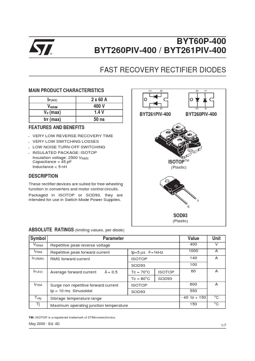
TURN-OFF SWITCHING CHARACTERISTICS
Symbol tIRM
IRM
Parameter Maximum reverse recovery time
Maximum reverse recovery current
C = VRP VCC
Turn-off overvoltage coefficient
ISOTOP SOD93
Storage temperature range
Maximum operating junction temperature
Value 400 1000 140 100 60
600 550 - 40 to + 150 150
Unit V A A
A
A
°C °C
TM: ISOTOP is a registered trademark of STMicroelectronics.
Insulation voltage: 2500 VRMS Capacitance = 45 pF Inductance < 5 nH
ISOTOPTM (Plastic)
DESCRIPTION
These rectifier devices are suited for free-wheeling function in converters and motor control circuits. Packaged in ISOTOP or SOD93, they are intended for use in Switch Mode Power Supplies.
Test Conditions
dIF/dt = - 240 A/µs dIF/dt = - 480 A/µs dIF/dt = - 240 A/µs dIF/dt = - 480 A/µs
pm75b4lb060_e

INSULATED PACKAGEINSULATED PACKAGEParameterSymbolSupply Voltage Protected bySCSupply Voltage (Surge)Storage Temperature Isolation Voltage ConditionV CC(surge)T stgV iso Ratings V CC(PROT)400500–40 ~ +1252500Unit V °C V rmsV V D = 13.5 ~ 16.5V, Inverter Part,T j = +125°C StartApplied between : P-N, Surge value60Hz, Sinusoidal, Charged part to Base, AC 1 min.——3.31.40.20.41.80.4110Min.Typ.Max.Collector-Emitter Saturation Voltage Collector-Emitter Cutoff Current–I C = 75A, V D = 15V, V CIN = 15V (Fig. 2)T j = 25°C T j = 125°CELECTRICAL CHARACTERISTICS (Tj = 25°C, unless otherwise noted)INVERTER PARTParameterSymbol ConditionV CE(sat)I CESV ECt on t rr t c(on)t off t c(off)Limits ———0.3——————1.71.552.20.70.10.20.90.2——T j = 25°C T j = 125°CFWDi Forward VoltageSwitching TimeV D = 15V, V CIN = 0V ↔15V V CC = 300V, I C = 75A T j = 125°C Inductive Load (Fig. 3,4)V CE = V CES , V CIN = 15V(Fig. 5)V D = 15V, I C = 75A V CIN = 0V (Fig. 1)TOTAL SYSTEMV mAVµsUnit 0.320.530.038°C/WR th(j-c)Q R th(j-c)F R th(c-f)Inverter IGBT part (per 1/4 module) (Note-1)Inverter FWDi part (per 1/4 module) (Note-1)Case to fin, (per 1 module)Thermal grease applied(Note-1)Symbol ConditionUnitMin.——————Junction to case Thermal ResistancesTHERMAL RESISTANCESContact Thermal Resistance(Note-1) Tc (under the chip) measurement point is below.ParameterLimits Typ.Max.UPIGBT 30.4–8.3VPUNVNFWDi30.4–0.8IGBT 61.7–8.3FWDi61.7–0.8IGBT 39.76.3FWDi39.7–1.2IGBT 52.46.3FWDi52.4–1.2armaxisX Y(unit : mm)Bottom viewINSULATED PACKAGEV D = 15VDetect T j of IGBT chip –20 ≤ T j ≤ 125°C V D = 15V, V FO = 15V (Note-2)V D = 15V(Note-2)V th(ON)V th(OFF)SC t off(SC)OT OT r UV UV r I FO(H)I FO(L)t FOTrip level Reset level Trip level Reset level–20 ≤ T j ≤ 125°C, V D = 15V (Fig. 3,6)V D = 15V(Fig. 3,6) 3.5———Mounting partscrew : M5—Symbol ParameterMounting torque WeightConditionUnit N • m gLimits Min.Typ.Max.2.5—3.0340MECHANICAL RATINGS AND CHARACTERISTICSV D = 15V, V CIN = 15VApplied between :U P -V UPC , V P -V VPCU N • V N -V NCI D °C V mA ms25121.82.3————12.5—0.0115—mA Circuit CurrentInput ON Threshold Voltage Input OFF Threshold Voltage Short Circuit Trip Level Short Circuit Current Delay TimeOver Temperature Protection Supply Circuit Under-Voltage ProtectionFault Output Current Minimum Fault Output Pulse WidthCONTROL PART——1.21.7150—135—11.5———1.0ParameterSymbol ConditionMax.Min.Typ.Unit Limits 1561.52.0—0.214512512.012.5—101.8(Note-2)Fault output is given only when the internal SC, OT & UV protections schemes of either upper or lower arm device operate toprotect it.V µs V N1-V NC V *P1-V *PCA RECOMMENDED CONDITIONS FOR USERecommended valueUnit ConditionSymbol ParameterV Applied across P-N terminalsApplied between :V UP1-V UPC , V VP1-V VPCV N1-V NC(Note-3)Applied between :U P -V UPC , V P -V VPCU N • V N -V NC Using Application Circuit of Fig. 8For IPM ’s each input signals(Fig. 7)Supply Voltage Control Supply Voltage Input ON Voltage Input OFF Voltage PWM Input Frequency Arm Shoot-through Blocking Time≤ 40015±1.5≤ 0.8≥ 9.0≤ 20≥ 2.0V CC V CIN(ON)V CIN(OFF)f PWM t deadV D V kHz µsV (Note-3)With ripple satisfying the following conditions : dv/dt swing ≤ ±5V/µs, Variation ≤ 2V peak to peakINSULATED PACKAGEINSULATED PACKAGEINSULATED PACKAGEINSULATED PACKAGE。
- 1、下载文档前请自行甄别文档内容的完整性,平台不提供额外的编辑、内容补充、找答案等附加服务。
- 2、"仅部分预览"的文档,不可在线预览部分如存在完整性等问题,可反馈申请退款(可完整预览的文档不适用该条件!)。
- 3、如文档侵犯您的权益,请联系客服反馈,我们会尽快为您处理(人工客服工作时间:9:00-18:30)。
Collector current : Ic [A]
IGBT Module
Collector current vs. Collector-Emitter voltage (typ.) Tj= 125°C / chip
1000
VGE=20V15V 12V 800
10V 600
400
200
0 0
8V
1
2
元器件交易网
2MBI400U2B-060
IGBT Module U-Series 600V / 400A 2 in one-package
2. Equivalent circuEit quivalent Circuit Schematic
Features
· High speed switching · Voltage drive · Low inductance module structure
IGBT Module
10000
Switching time vs. Collector current (typ.) Vcc=300V, VGE=±15V, Rg=6.8Ω, Tj= 25°C
Switching time vs. Collector current (typ.) Vcc=300V, VGE=±15V, Rg=6.8Ω, Tj=125°C
Collector current : Ic [A]
600
10V
400
200
0 0
8V
1
2
3
4
5
Collector-Emitter voltage : VCE [V]
Collector current : Ic [A]
Collector current vs. Collector-Emitter voltage (typ.) VGE=15V / chip
Rth(j-c) Rth(j-c) Rth(c-f)*4
IGBT FWD With thermal compound
Min. – – –
Typ. – – 0.025
*4 : This is the value which is defined mounting on the additional cooling fin with thermal compound.
Max. 2.0
400 7.7 2.55 – – – – 1.20 0.60 – 1.20 0.45 2.35 – – – 0.35 –
Max. 0.10 0.16 –
Unit V V A
W °C VAC N·m
Unit mA nA V V
nF µs
V
µs mΩ
Unit °C/W °C/W °C/W
10
15
20
25
Gate - Emitter voltage : VGE [ V ]
Dynamic Gate charge (typ.) Vcc=300V, Ic=400A, Tj= 25°C
VGE
VCE
0
400
800
1200
1600
Gate charge : Qg [ nC ]
元器件交易网 2MBI400U2B-060
Reverse recovery current : Irr [ A ] Reverse recovery time : trr [ nsec ]
Reverse recovery characteristics (typ.) Vcc=300V, VGE=±15V, Rg=6.8Ω
1000
trr (125°C)
AC:1min.
Screw Torque
Mounting *2
Terminals *2
*1 : All terminals should be connected together when isolation test will be done.
*2 : Recommendable value : Mounting 2.5 to 3.5N·m(M5), Terminal 2.5 to 3.5 N·m(M5)
Turn-off time Forward on voltage
Reverse recovery time Lead resistance, terminal-chip*3
ICES IGES VGE(th) VCE(sat) (terminal) VCE(sat) (chip) Cies ton tr tr(i) toff tf VF (terminal) VF (chip) trr R lead
1000
800
600
400
200
0
0
200
400
600
800
Collector - Emitter voltage : VCE [ V ]
Switching loss : Eon, Eoff, Err [ mJ/pulse ]
元器件交易网 2MBI400U2B-060
IGBT Module
VGES IC ICp
Continuous 1ms
-IC
Collector Power Dissipation
-IC pulse PC
1 device
Junction temperature
Tj
Storage temperature
Tstg
Isolation voltage between terminal and copper base *1 Viso
Rating 650 ±20 400 800 400 800
1250 +150 -40 to +125 2500
3.5 3.5
Electrical characteristics (at Tj=25°C unless otherwise specified)
Item
Symbols Conditions
1000
800
Tj=25°C Tj=125°C
600
400
200
0
0
1
2
3
4
Collector-Emitter voltage : VCE [V]
Capacitance vs. Collector-Emitter voltage (typ.)
100.0 10.0 1.0
Cies
Cres Coes
Capacitance : Cies, Coes, Cres [ nF ]
元器件交易网
2MBI400U2B-060
Characteristics (Representative)
Collector current vs. Collector-Emitter voltage (typ.) Tj= 25°C / chip
1000
800
VGE=20V15V 12V
0.1 0
10
20
30
Collector-Emitter voltage : VCE [V]
Collector-Emitter voltage : VCE [ 100V/div ] Gate - Emitter voltage : VGE [ 5V/div ]
Collector - Emitter voltage : VCE [ V ]
10.0 Gate resistance : Rg [ Ω ]
100.0
Switching loss vs. Gate resistance (typ.) Vcc=300V, Ic=400A, VGE=±15V, Tj= 125°C
60
50
Eon
40
30
Eoff
20
10
0 1.0
10.0 Gate resistance : Rg [ Ω ]
Forward current : IF [ A ]
a Forward current vs. Forward on voltage (typ.) chip
1000
800 Tj=25°C Tj=125°C
600
400
200
0
0.0
1.0
2.0
3.0
Forward on voltage : VF [ V ]
10 0
200
400
600
800
Collector current : Ic [ A ]
10000
Switching time vs. Gate resistance (typ.) Vcc=300V, Ic=400A, VGE=±15V, Tj= 25°C
1000
tr
toff
ton
tf
100
10 1.0
Characteristics
Zero gate voltage collector current Gate-Emitter leakage current Gate-Emitter threshold voltage Collector-Emitter saturation voltage
Input capacitance Turn-on time
Err 100.0
Collector current : Ic [ A ]
Switching loss : Eon, Eoff, Err [ mJ/pulse ]
10 0
200
400
600
800
Collector current : Ic [ A ]
Switching loss vs. Collector current (typ.) Vcc=300V, VGE=±15V, Rg=6.8Ω
