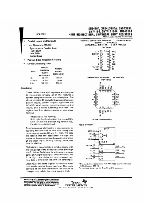
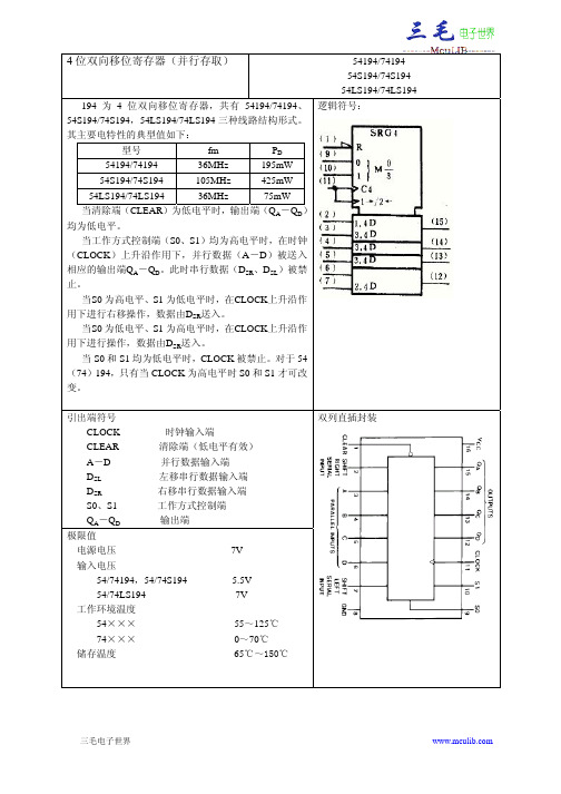
DM74LS194中文资料
移位寄存器194

一、74LS194的功能 的功能
二、74LS194构成环形计数器 构成环形计数器
Q 0 Q 1 Q 2 Q 3
74 L S 19 4 SR
C P
把移位寄存器的输出反馈到它的串行输入端, 把移位寄存器的输出反馈到它的串行输入端,就可以进行循 环移位,如图所示,把输出端Q 和右移串行输入端S 相连接, 环移位,如图所示,把输出端Q3 和右移串行输入端SR 相连接, 设初始状态Q =1000,则在时钟脉冲作用下 则在时钟脉冲作用下Q 设初始状态Q0Q1Q2Q3=1000,则在时钟脉冲作用下Q0Q1Q2Q3将依次 边为0100→0010→0001→1000→````` 如图所示, 0100→0010→0001→1000→`````, 边为0100→0010→0001→1000→`````,如图所示,可见它是一 个具有四个有效状态的计数器, 个具有四个有效状态的计数器,这种类型的计数器通常称为环 形计数器。 形计数器。
两片74LS194扩展为 位移位寄存器 扩展为8位移位寄存器 三、两片 扩展为
两片74LS194实现串并转换器 四、两片 实现串并转换器
两片7转换器
移位寄存器实验预习报告要求: 移位寄存器实验预习报告要求:
1、画出74194功能测试的功能表格 、画出 功能测试的功能表格 2、画出由 、画出由74194构成环形计数器的接线图 构成环形计数器的接线图 3、画出两片 扩展成8位的移位寄存器的 、画出两片74194扩展成 位的移位寄存器的 扩展成 接线图 4、画出用两片 构成的七位左移 、画出用两片74194构成的七位左移串/并行 构成的七位左移串 并行 转换器接线路。 转换器接线路。 5、画出用两片 构成的七位左移 、画出用两片74194构成的七位左移并/串行 构成的七位左移并 串行 转换器接线路。 转换器接线路。
74LS194中文资料_数据手册_参数
74LS194是一种高速4位双向通用移位寄存器。
作为一种高速、多功能的顺序构建块,它在许多应用中都很有用。
它可以用于插入-串行、左移、右移、串行-并行、并行-串行和并行-并行数据寄存器传输。
LS194A类似于LS195A通用移位寄存器,增加了没有外部连接的移位和保持(什么也不做)modesof操作的功能。
74LS194它利用肖特基二极管夹紧工艺实现高速,并完全兼容于所有的半导体晶体管家族。
•典型的移频为36mhz•异步主复位•保持(什么也不做)模式•完全同步串行或并行数据传输•输入箝位二极管限制高速终止效果逻辑图和真值表显示了LS194A四位双向移位寄存器的功能特性。
LS194A在操作上类似于席恩半导体LS195A通用移位寄存器,用于串行或并行数据寄存器传输。
这两种设备的一些共同特征如下:所有数据和模式控制输入都是边缘触发的,只响应时钟的低到高转换(CP)。
因此,唯一的时间限制是modecontrol和所选的数据输入必须在时钟脉冲正转换之前的一个设置时间是稳定的。
寄存器是完全同步的,所有操作都在15 ns以内(通常),这使得设备对于实现高速cpu或内存缓冲寄存器特别有用。
74LS194四个并行数据输入(P0、P1、P2、P3)是d类型的输入。
当S0和S1都很高时,出现在P0、P1、P2和P3输入上的数据在时钟的下一个低到高的跃迁之后分别被传输到Q0、Q1、Q2和Q3输出。
异步主重置(MR)在低时覆盖所有其他输入条件,并强制Q输出变慢。
增加应用范围的LS194A设计的特殊逻辑特性描述如下:两个模式控制输入(S0, S1)决定设备的同步运行。
如ModeSelection表所示,数据可以从左到右(右移,Q0!)Q1,等等)或者从右向左(左移,Q3!,或者可以输入并行数据,同时加载寄存器的所有四位。
当S0和S1都很低时,74LS194现有的数据被保留在一个“什么也不做”的模式中,而不限制从高到低的时钟转换。
74LS194左右移位寄存器
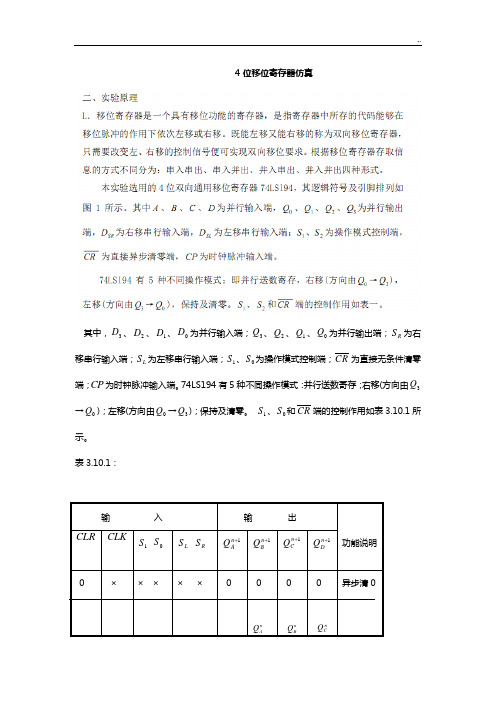
4位移位寄存器仿真其中,3D 、2D 、1D 、0D 为并行输入端;3Q 、2Q 、1Q 、0Q 为并行输出端;R S 为右移串行输入端;L S 为左移串行输入端;1S 、0S 为操作模式控制端;R C 为直接无条件清零端;CP 为时钟脉冲输入端。
74LS194有5种不同操作模式:并行送数寄存;右移(方向由3Q →0Q );左移(方向由0Q →3Q );保持及清零。
1S 、0S 和R C 端的控制作用如表3.10.1所示。
表3.10.1:输 入 输 出功能说明CLR CLK1S 0S L S R S 1+n A Q 1+n B Q 1+n C Q 1+n D Q 0 × × × × × 0 0 n AQ 0 n B Q 0 n C Q 异步清0移位寄存器应用很广,可构成移位寄存器型计数器;顺序脉冲发生器;串行累加器;可用作数据转换,即把串行数据转换为并行数据,或并行数据转换为串行数据等。
把移位寄存器的输出反馈到它的串行输入端,就可进行循环移位,如图3.10.2所示。
把输出端0Q 和右移串行输入端R S 相连接,设初始状态3Q 2Q 1Q 0Q =1000,则在时钟脉冲作用下,3Q 2Q 1Q 0Q 将依次变为0100→0010→0001→1000→……,可见,它是一个具有四个有效状态的计数器,这种类型的计数器通常称为环形计数器。
图3.10.2电路可以由各个输出端输出在时间上有先后顺序的脉冲,因此也可作为顺序脉冲发生器。
图3.10.2四、实验室操作实验内容:1.逻辑功能验证移位寄存器(1)将两块74LS74集成片插入IC空插座中,按图41(a)连线,接成左移移位寄存器。
接好电源即可开始实验。
先置数据0001,然后输入移位脉冲。
置数,即把Q3、Q2、Q1、Q0置成0001,按动单次脉冲,移位寄存器实现左移功能。
(2)按图42(b)连线,方法同(1)则完成右移移位功能验证。
74LS194芯片资料

单脉冲的提供有两种途径:
实验目的
逻辑箱脉冲源
单脉冲
实验原理
低频信号源TTL 输出(1Hz)
实验内容
注意事项
现代电子技术实验
四、注意事项
1、出现故障应作哪些基本检查? 电源
实验目的
时钟 功能端(Cr 、S1、 S0 ) 数据输入是否正确
实验原理
实验内容
注意事项
2、实验中的环形计数器不具备自启动功能,抗 干扰能力差。改变电路连接时如进入死循环,必 须给电路重新赋初值。
实验目的
DSR
清零 置数
CP
0 1
DR
1 1
DL
1 1
Q0
0 0
Q1
0 1
Q2
0 0
Q3
0 1
实验原理
左移
实验内容
2 3
4
0 0
1
0 0
1
左移
右移
注意事项
右移 保持
5 6
1 0
1 0
现代电子技术实验
2、环形计数器的测试。首先应给寄存器置入初始 值(自拟),之后将工作状态设为对应的串行移 位,完成下表。
现代电子技术实验
移位寄存器的扩展
实验目的
实验原理
ห้องสมุดไป่ตู้
74LS194(1)
实验内容
74LS194(2)
注意事项
串行输入
构成八位右移串行移位寄存器
现代电子技术实验
2、环形计数器(又称循环移位寄存器)
把移位寄存器的串行输入端与输出端相连可以 构成环形计数器。例:DSR和Q3相连,可构成右移环 形计数器。
实验目的
n 2
0 X X
74ls194寄存器逻辑功能测试实验原理 -回复
74ls194寄存器逻辑功能测试实验原理-回复74LS194寄存器逻辑功能测试实验原理一、简介74LS194是一种集成电路芯片,属于74系列的高速并行数据输入和串行输出寄存器。
它具有多种逻辑功能,包括数据输入、输出、锁存等。
在数字电路实验中,通常需要对这类芯片进行逻辑功能测试,以验证其是否正常工作。
本实验将介绍如何进行74LS194寄存器的逻辑功能测试,并解释其实验原理。
二、实验器材与测量工具1. 实验器材- 74LS194寄存器芯片- 蜂鸣器- 杜邦线- 面包板- 电源模块2. 测量工具- 逻辑分析仪- 示波器- 万用表- 信号发生器三、实验步骤1. 搭建电路将74LS194芯片插入面包板,并根据芯片的引脚定义连线。
具体电路连接方式如下:- 引脚1和引脚16接地;- 引脚2连接信号发生器的输出端;- 引脚3和引脚4分别连接示波器的通道1和通道2;- 引脚5、引脚6和引脚7连接蜂鸣器;- 引脚8、引脚9、引脚10和引脚11分别连接示波器的通道3、通道4、通道5和通道6;- 引脚12和引脚13分别连接逻辑分析仪的输入端;- 引脚14和引脚15连接电源正负极。
2. 设置信号发生器根据74LS194的信号输入要求,设置信号发生器的输出为有效的高电平和低电平信号。
这里可以设置输出频率为1kHz,并将占空比设置为50。
这样可以确保产生的信号满足寄存器芯片的要求。
3. 运行测试程序使用信号发生器给74LS194芯片输入信号。
首先,输入序列的时间长度为16个时钟周期,通过示波器监测输入序列的波形,确保信号输入正确。
然后,将信号发生器的输出与74LS194芯片的D0引脚相连接,将示波器的通道1选择为D0信号。
通过示波器监测D0信号的波形,确保输入信号成功进入寄存器。
接下来,使用逻辑分析仪监测寄存器的输出数据。
将逻辑分析仪的输入端分别与74LS194芯片的Q0到Q7引脚连接。
通过逻辑分析仪,可以实时观察寄存器的输出数据,并验证其是否与输入数据一致。
74ls194寄存器逻辑功能测试实验原理
74ls194寄存器逻辑功能测试实验原理一、实验目的本实验旨在测试74LS194寄存器的逻辑功能,了解其工作原理和特点,为实际应用提供理论依据。
二、实验原理74LS194寄存器是一种双四位同步可逆计数器,具有以下特点:1. 包含两个独立的四位二进制计数器,每个计数器都可以独立工作。
2. 每个计数器由四个触发器和两个与非门组成,采用异步清零和同步置数/保持/清零操作方式。
3. 可进行正、反向计数,具有计数保持功能。
4. 具备控制端,可用于选择计数器、置数、保持或清零操作。
1. 输入/输出逻辑关系:74LS194寄存器共有16个输入端(A3-A0、BCDEG、CE),6个输出端(Q3-Q0、QC3-QC0),可通过控制信号和输入信号的变化,观察输出端的变化情况,从而测试其逻辑功能。
2. 工作原理:当74LS194复位(CE=0)时,所有输出端均为低电平(Q3-Q0、QC3-QC0=0)。
当向A3-A0任意一个输入端输入高电平(1)时,对应的十进制数被置入到高位计数器(GCD)中。
同时,置数端(GND)为低电平(GND),高四位触发器开始同步递增计数(时钟脉冲上升沿时),同时向低位计数器传输相应的数字。
当低位计数器达到最大值(1111)时,需要反向计数或置数清零,此时高位计数器的数字将传递给低位计数器。
当需要反向计数时,控制端(NOT A3-A0)为高电平(0),此时高位计数器的数字将反向传递给低位计数器。
当需要清零时,控制端(CE=1)会将所有输出端拉低电平。
此外,控制端还可以选择保持或清零操作,保持状态时,当时钟脉冲上升沿来临时,高四位触发器将按原方向继续递增计数;当处于清零状态时,所有输出端被强制拉低电平。
三、实验步骤1. 准备实验器材:74LS194寄存器芯片、测试板、电源模块、连接线等。
2. 连接电路:将74LS194芯片焊接在测试板上,根据其引脚定义连接相应的电源线和数据线。
3. 输入测试信号:通过控制台输入控制信号和输入信号,观察输出端的变化情况。
74ls194
54194/74194
54S194/74S194
194 为 4 位双向移位寄存器,共有 54194/74194、 54S194/74S194,54LS194/74LS194 三种线路结构形式。 其主要电特性的典型值如下:
54LS194/74LS194 逻辑符号:
型号 54194/74194
23
单位 V V V mA µA mA mA mA
动态特性(TA=25℃)
参
数[2]
测试条件
‘194
‘S194
‘LS194
单位
最小 最大 最小 最大 最小 最大
fmax
Vcc =5V,CL=15Pf,RL=400Ω 25
70
25
MHz
tPLH CLOCK → 任一 (‘194 为 280Ω,‘LS194 为
引出端符号
CLOCK
时钟输入端
CLEAR A-D
清除端(低电平有效) 并行数据输入端
DSL DSR S0、S1 QA-QD 极限值
左移串行数据输入端 右移串行数据输入端 工作方式控制端 输出端
电源电压
7V
输入电压
54/74194,54/74S194
5.5V
54/74LS194
7V
工作环境温度
54××× 74×××
0.4 0.4
0.5 0.5
II最大输入电压时输入电 Vcc=最大 流
IIH输入高电平电流
Vcc=最大
VI=5.5V VI=7V VIH=2.4V VIH=2.7V
1
1
40 50
IIL输入低电平电流
Vcc=最大,
VIL=0.4V VIL=0.5V
彩灯循环显示电路74ls194
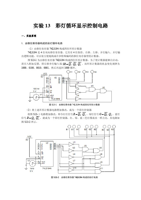
实验13 彩灯循环显示控制电路一、实验原理1. 由移位寄存器构成的彩灯循环电路(1)由移位寄存器74LS194构成四位环形计数器74LS194是4位双向移位寄存器。
它具有4位保持、右移、左移、并行输入、并行输出逻辑功能,可以很方便地构成许多特殊编码的移位寄存器型的计数器。
图S13-1为由移位寄存器74LS194构成四位环形计数器。
为了使计数器能够自启动,需引入附加反馈,即右移串行输入端C B A SR Q Q Q =⋅⋅。
该环形计数器的状态变化规律为1000、0100、0010、0001,然后再返回1000循环。
图S13-1 由移位寄存器74LS194构成四位环形计数器(2)将上述环形计数器电路稍加修改,成为一个彩灯控制器将图S13-1电路稍加修改,即令红灯信号B A R Q Q =⋅,绿灯信号B A G Q Q =⋅,蓝灯信号B A B Q Q =⋅,就成为一个彩灯控制器,红、绿、蓝三色灯像流水一样点亮,其电路如图S13-2所示。
图S13-2 由移位寄存器74L S194构成的彩灯电路2.由计数器和译码器构成的旋转彩灯电路图S13-3电路是由四位同步二进制计数器74LS163和3线-8线译码器74LS138构成,计数器的输出端QC、QB、QA分别接译码器的代码输入端C、B、A,译码器的输出端接LED。
图S13-3 由计数器和译码器构成的旋转彩灯电路图S13-4 Multisim10.0界面中逻辑分析仪观察旋转彩灯电路的输出结果3.双色循环彩灯电路本控制器由计数器、译码器、LED 显示电路等组成。
其框图如图S13-5所示。
图S13-5 双色循环彩灯电路框图(1)计数器部分由芯片CC4516组成。
CC4516是可预置数的4位二进制加/减计数器,它有5种功能:置数、清零、不计数、加法计数、减法计数。
在本实验中其电路如图S13-6所示。
图S13-6 Multisim10.0界面中计数器部分的电路结构(2)译码器由芯片CC4514组成,它是4位锁存/4线-16线译码器,具有数据锁存、译码和禁止输出3种功能,其输出为高电平有效。
74LS194

实验原理
实验内容
注意事项
现代电子技术实验
实验目的
实验原理
74LS194
实验内容
注意事项
逻辑符号
引脚图
移位寄存器存取信息的方式有:串入串出、串入并 出、并入串出、并入并出四种形式。
现代电子技术实验
输出端
时 钟
控制信号
实验目的
实验原理
74LS194 74LS194
实验内容
注意事项
清 零 端
右 移 串 行 输 入
0
0 0
1
0 0
0
1 0
0
注意事项
5
74LS194
现代电子技术实验
把移位寄存器的输出端Q3和DSR相连,可构成 简单的右移环形计数器。若把移位寄存器的输出 端Q0和DSL相连,可构成简单的左移环形计数器。
实验目的
实验原理
实验内容
注意事项
三、实验内容
现代电子技术实验
1、基本功能测试。要求针对74LS194各项基本功能。
1000
有效 状态
0100
00000001Fra bibliotek0010
0 1 74X194
该电路不能自启动
现代电子技术实验
首先应给输出端赋初值,此时S1 S0为11。
再将S1 S0改为01,使之工作在右移状态。
实验目的
CP 1
1
Q0 1 0
Q1 0 1
Q2 0 0
Q3 0 0
实验原理
0 0
2
实验内容
3
4
0 1
0
0 1
n
现代电子技术实验
移位寄存器的扩展
实验目的
74194 TTL 四位双向通用移位寄存器
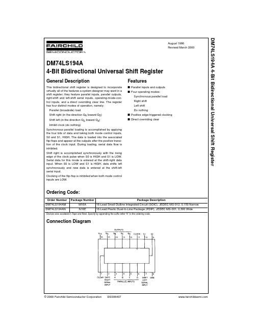
© 2000 Fairchild Semiconductor Corporation DS006407August 1986Revised March 2000DM74LS194A 4-Bit Bidirectional Universal Shift RegisterDM74LS194A4-Bit Bidirectional Universal Shift RegisterGeneral DescriptionThis bidirectional shift register is designed to incorporate virtually all of the features a system designer may want in a shift register; they feature parallel inputs, parallel outputs,right-shift and left-shift serial inputs, operating-mode-con-trol inputs, and a direct overriding clear line. The register has four distinct modes of operation, namely:Parallel (broadside) loadShift right (in the direction Q A toward Q D )Shift left (in the direction Q D toward Q A )Inhibit clock (do nothing)Synchronous parallel loading is accomplished by applying the four bits of data and taking both mode control inputs,S0 and S1, HIGH. The data is loaded into the associated flip-flops and appear at the outputs after the positive transi-tion of the clock input. During loading, serial data flow is inhibited.Shift right is accomplished synchronously with the rising edge of the clock pulse when S0 is HIGH and S1 is LOW.Serial data for this mode is entered at the shift-right data input. When S0 is LOW and S1 is HIGH, data shifts left synchronously and new data is entered at the shift-left serial input.Clocking of the flip-flop is inhibited when both mode control inputs are LOW.Featuress Parallel inputs and outputs s Four operating modes:Synchronous parallel load Right shift Left shiftDo nothings Positive edge-triggered clocking s Direct overriding clearOrdering Code:Devices also available in Tape and Reel. Specify by appending the suffix letter “X” to the ordering code.Connection DiagramOrder Number Package NumberPackage DescriptionDM74LS194AM M16A 16-Lead Small Outline Integrated Circuit (SOIC), JEDEC MS-012, 0.150 Narrow DM74LS194ANN16E16-Lead Plastic Dual-In-Line Package (PDIP), JEDEC MS-001, 0.300 Wide 2D M 74L S 194AFunction TableH = HIGH Level (steady state)L = LOW Level (steady state)X = Don’t Care (any input, including transitions)↑ = Transition from LOW-to-HIGH levela, b, c, d = The level of steady state input at inputs A, B, C or D, respectively.Q A0, Q B0, Q C0, Q D0 = The level of Q A , Q B , Q C , or Q D , respectively, before the indicated steady state input conditions were established.Q An , Q Bn , Q Cn , Q Dn = The level of Q A , Q B , Q C , respectively, before the most-recent ↑ transition of the clock.Logic DiagramInputsOutputs Clear Mode Clock Serial Parallel Q A Q B Q C Q D S1S0Left Right A B C D L X X X X X X X X X L L L L H X X L X X X X X X Q A0Q B0Q C0Q D0H H H ↑X X a b c d a b c d H L H ↑X H X X X X H Q An Q Bn Q Cn H L H ↑X L X X X X L Q An Q Bn Q Cn H H L ↑H X X X X X Q Bn Q Cn Q Dn H H H L ↑L X X X X X Q Bn Q Cn Q Dn L HLLXXXXXXXQ A0Q B0Q C0Q D0DM74LS194AAbsolute Maximum Ratings (Note 1)Note 1: The “Absolute Maximum Ratings” are those values beyond which the safety of the device cannot be guaranteed. The device should not be operated at these limits. The parametric values defined in the Electrical Characteristics tables are not guaranteed at the absolute maximum ratings.The “Recommended Operating Conditions” table will define the conditions for actual device operation.Recommended Operating ConditionsNote 2: C L = 15 pF, T A = 25°C and V CC = 5V.Note 3: C L = 50 pF, R L = 2 k Ω, T A = 25°C and V CC = 5V.Note 4: T A = 25°C and V CC = 5V.Electrical Characteristicsover recommended operating free air temperature range (unless otherwise noted)Note 5: All typicals are at V CC = 5V, T A = 25°C.Note 6: Not more than one output should be shorted at a time, and the duration should not exceed one second.Note 7: With all outputs open, inputs A through D grounded, and 4.5V applied to S0, S1, CLEAR, and the serial inputs, I CC is tested with momentary ground,then 4.5V applied to CLOCK.Supply Voltage 7V Input Voltage7VOperating Free Air Temperature Range 0°C to +70°C Storage Temperature Range−65°C to +150°CSymbol ParameterMin Nom Max Units V CC Supply Voltage4.7555.25V V IH HIGH Level Input Voltage 2V V IL LOW Level Input Voltage 0.8V I OH HIGH Level Output Current −0.4mA I OL LOW Level Output Current 8mA f CLK Clock Frequency (Note 2)025MHz Clock Frequency (Note 3)020t W Pulse Width Clock 20ns (Note 4)Clear 20t SU Setup Time Mode 30ns (Note 4)Data20t H Hold Time (Note 4)0ns t REL Clear Release Time (Note 4)25ns T AFree Air Operating Temperature70°CSymbol ParameterConditionsMinTyp Max Units (Note 5)V I Input Clamp Voltage V CC = Min, I I = −18 mA −1.5V V OH HIGH Level V CC = Min, I OH = Max 2.73.4VOutput Voltage V IL = Max, V IH = Min V OLLOW Level V CC = Min, I OL = Max 0.350.5Output VoltageV IL = Max, V IH = Min VI OL = 4 mA, V CC = Min 0.4I I Input Current @ Max Input Voltage V CC = Max, V I = 7V 0.1mA I IH HIGH Level Input Current V CC = Max, V I = 2.7V 20µA I IL LOW Level Input Current V CC = Max, V I = 0.4V −0.4mA I OS Short Circuit Output Current V CC = Max (Note 6)−20−100mA I CCSupply CurrentV CC = Max (Note 7)1523mA 4D M 74L S 194ASwitching Characteristicsat V CC = 5V and T A = 25°C Note 8: All typicals are at V CC = 5V, T A = 25°C.Note 9: Not more than one output should be shorted at a time, and the duration should not exceed one second.Note 10: With all outputs open, inputs A through D grounded, and 4.5V applied to S0, S1, CLEAR, and the serial inputs, I CC is tested with momentary ground, then 4.5V applied to CLOCK.Timing DiagramTypical Clear, Load, Right-Shift, Left-Shift, Inhibit, and Clear SequencesSymbol ParameterFrom (Input)C L = 50 pF, R L = 2 k ΩUnits To (Output)Min Maxf MAX Maximum Clock Frequency 20MHz t PLH Propagation Delay Time Clock to Any Q 26ns LOW-to-HIGH Level Output t PHL Propagation Delay Time Clock to Any Q 35ns HIGH-to-LOW Level Output t PHLPropagation Delay Time Clear to Any Q38nsHIGH-to-LOW Output DM74LS194APhysical Dimensions inches (millimeters) unless otherwise noted16-Lead Small Outline Integrated Circuit (SOIC), JEDEC MS-012, 0.150 NarrowPackage Number M16A6D M 74L S 194A 4-B i t B i d i r e c t i o n a l U n i v e r s a l S h i f t R e g i s t e rPhysical Dimensions inches (millimeters) unless otherwise noted (Continued)16-Lead Plastic Dual-In-Line Package (PDIP), JEDEC MS-001, 0.300 WidePackage Number N16EFairchild does not assume any responsibility for use of any circuitry described, no circuit patent licenses are implied and Fairchild reserves the right at any time without notice to change said circuitry and specifications.LIFE SUPPORT POLICYFAIRCHILD’S PRODUCTS ARE NOT AUTHORIZED FOR USE AS CRITICAL COMPONENTS IN LIFE SUPPORT DEVICES OR SYSTEMS WITHOUT THE EXPRESS WRITTEN APPROVAL OF THE PRESIDENT OF FAIRCHILD SEMICONDUCTOR CORPORATION. As used herein:1.Life support devices or systems are devices or systems which, (a) are intended for surgical implant into the body, or (b) support or sustain life, and (c) whose failure to perform when properly used in accordance with instructions for use provided in the labeling, can be rea-sonably expected to result in a significant injury to the user. 2. A critical component in any component of a life support device or system whose failure to perform can be rea-sonably expected to cause the failure of the life support device or system, or to affect its safety or effectiveness.。
74ls194功能
74ls194功能
74LS194是一种具有四个主要功能的16位边缘触发通用串行-
并行移位寄存器。
以下是74LS194的主要功能:
1. 并行输入:74LS194有16个并行输入引脚,称为A0-A15,
可以同时将16位数据并行输入到寄存器中。
2. 串行输入:74LS194有一个串行输入引脚,称为D。
通过串
行输入,可以逐位输入的方式将数据输入到寄存器中。
3. 串行输出:74LS194有一个串行输出引脚,称为Q。
通过串
行输出引脚,可以逐位输出寄存器中的数据。
4. 并行输出:74LS194有16个并行输出引脚,称为Q0-Q15。
可以同时从寄存器中将16位数据并行输出。
5. 移位功能:74LS194具有向左和向右移位的能力。
通过控制
引脚,可以选择移位方向。
6. 边缘触发:74LS194是边缘触发器件,这意味着它只在时钟
信号的边沿触发数据输入和输出。
可以通过时钟引脚控制寄存器的操作。
7. 计数功能:74LS194可以用作计数器。
通过适当连接控制引脚,可以将多个74LS194级联,以实现更大范围的计数器。
8. 加载功能:74LS194可以将并行输入的数据加载到寄存器中,
而不进行移位操作。
总而言之,74LS194是一个功能强大的通用寄存器,可以实现并行输入、并行输出、串行输入、串行输出、移位和计数等多种功能。
它适用于广泛的应用,如数据存储和计数器设计。
74LS194左右移位寄存器

74LS194左右移位寄存器一、移位寄存器在数字电路中,用来存放二进制数据或代码的电路称为寄存器。
按功能可分为:基本寄存器和移位寄存器。
移位寄存器中的数据可以在移位脉冲作用下一次逐位右移或左移,数据既可以并行输入、并行输出,也可以串行输入、串行输出,还可以并行输入、串行输出,串行输入、并行输出,十分灵活,用途也很广。
二、74LS194双向移位寄存器目前常用的集成移位寄存器种类很多,其中74LS194为四位双向移存器。
图一74LS194移位寄存器的引脚图以上为74LS194的引脚图,其中D0~D3:并行输入端;Q0~Q3:并行输出端;S0、S1:操作模式控制端;:为直接无条件清零端;SR:右移串行输入端SL:xx串行输入端;CP:时钟脉冲输入端;表一74LS194的模式控制和状态输出表三、移位寄存器型计数器利用移位寄存器可构成环形和扭环形计数器。
可先使S0=S1=1,并行输入预置数值,再改变S0和S1的电平,实现左移或右移状态。
若把移位寄存器的输出以一定方式反馈到串行输入DSR端或DSL端,就可以构成移位寄存器型计数器。
例如,将74LS194的Q3接到DSR端,可得到模4的环形计数器(不可自启动);将Q3端通过一个非门接到DSR端,则可得到模8的扭环形计数器(不可自启动)。
用一片74LS194及门电路构成一个课实现7分频或8分频器。
7分频器的分频信号由Q2输出,同时将Q2、Q3输出通过与非门后接入DSR端,S0S1=10。
8分频器的分频信号由Q3取非后输出,同时将该信号送入D SR端,S0S1=10。
74ls194实验报告
74ls194实验报告74LS194实验报告引言:实验是科学研究的基础,通过实验我们可以验证理论,探索未知,提高我们的实践能力。
本次实验的主题是关于74LS194芯片的实验。
74LS194是一种4位双向移位寄存器,常用于数字电路设计和逻辑控制。
通过这次实验,我们将深入了解74LS194的原理和工作方式,并通过实际操作来验证其功能。
一、实验目的本次实验的目的是通过实际操作,深入了解74LS194芯片的工作原理和功能。
具体目标如下:1. 学习74LS194芯片的基本原理和功能;2. 掌握74LS194芯片的引脚定义和连接方式;3. 验证74LS194芯片的功能,包括数据输入、数据输出、移位操作等。
二、实验器材和材料1. 74LS194芯片;2. 电路连接板;3. 电源;4. 逻辑信号发生器;5. 示波器;6. 连接线。
三、实验步骤1. 连接电路:将74LS194芯片插入电路连接板,并根据实验原理图连接相应的电源和信号线。
2. 设置逻辑信号发生器:根据实验要求,设置逻辑信号发生器的输出频率和幅度。
3. 测量电压波形:使用示波器测量74LS194芯片的输出电压波形,并记录下相应的数据。
4. 进行数据输入操作:通过逻辑信号发生器输入相应的数据,观察74LS194芯片的输出是否正确。
5. 进行移位操作:通过逻辑信号发生器输入移位信号,观察74LS194芯片的输出是否正确。
6. 记录实验数据:将实验过程中的数据和观察结果记录下来,方便后续分析和总结。
四、实验结果与分析通过实验,我们得到了74LS194芯片的输出电压波形,并观察到了数据输入和移位操作的结果。
根据实验数据和观察结果,我们可以得出以下结论:1. 74LS194芯片能够正确地接收和输出数据,实现数据的存储和传输功能;2. 在进行移位操作时,74LS194芯片能够按照预期的方式将数据进行移位,并输出正确的结果;3. 在实验过程中,我们还发现了一些异常情况,例如输入信号的幅度过大或过小时,芯片可能无法正常工作。
交通灯控制_74LS194方案
Ag = Q5 Q6
Ay = Q5 Q6
Ar = Q6 Br = Q6 Bg = Q5Q6
By = Q5Q6
2012年3月2日
《脉冲与数字电路》实验指导
12
M=12
2012年3月2日
《脉冲与数字电路》实验指导
13
设计任务二
设A,B通道有红、绿(包括直行及右转绿灯G1, 左转绿灯G2)、黄四种灯,交通显示情况为: 1.A通道绿灯G1持续20秒,然后G2持续20秒;B通 道红灯;共40秒。 2.A通道黄灯,B通道红灯;共4秒。 3.A通道红灯, B通道绿灯G1持续20秒,然后G2持 续20秒;共40秒。 4.A通道红灯,B通道黄灯;共4秒。
4个状态
20个状态 A红 4个状态
B黄
2012年3月2日
《脉冲与数字电路》实验指导
11
12分频扭环型计数器
Q6 0 0 0 0 0 0 1 1 1 1 1 1 Q5 0 0 0 0 0 1 1 1 1 1 1 0 Q4 0 0 0 0 1 1 1 1 1 1 0 0 Q3 0 0 0 1 1 1 1 1 1 0 0 0 Q2 0 0 1 1 1 1 1 1 0 0 0 0 Q1 0 1 1 1 1 1 1 0 0 0 0 0 Ar 0 0 0 0 0 0 1 1 1 1 1 1 Ag 1 1 1 1 1 0 0 0 0 0 0 0 Ay 0 0 0 0 0 1 0 0 0 0 0 0 Br 1 1 1 1 1 1 0 0 0 0 0 0 Bg 0 0 0 0 0 0 1 1 1 1 1 0 By 0 0 0 0 0 0 0 0 0 0 0 1
3
二、实验仪器:
逻辑实验箱 万用表 双踪示波器 74LS00、74LS04、74LS10、74LS20 、 74LS194等.
- 1、下载文档前请自行甄别文档内容的完整性,平台不提供额外的编辑、内容补充、找答案等附加服务。
- 2、"仅部分预览"的文档,不可在线预览部分如存在完整性等问题,可反馈申请退款(可完整预览的文档不适用该条件!)。
- 3、如文档侵犯您的权益,请联系客服反馈,我们会尽快为您处理(人工客服工作时间:9:00-18:30)。
© 2000 Fairchild Semiconductor Corporation DS006407August 1986Revised March 2000DM74LS194A 4-Bit Bidirectional Universal Shift RegisterDM74LS194A4-Bit Bidirectional Universal Shift RegisterGeneral DescriptionThis bidirectional shift register is designed to incorporate virtually all of the features a system designer may want in a shift register; they feature parallel inputs, parallel outputs,right-shift and left-shift serial inputs, operating-mode-con-trol inputs, and a direct overriding clear line. The register has four distinct modes of operation, namely:Parallel (broadside) loadShift right (in the direction Q A toward Q D )Shift left (in the direction Q D toward Q A )Inhibit clock (do nothing)Synchronous parallel loading is accomplished by applying the four bits of data and taking both mode control inputs,S0 and S1, HIGH. The data is loaded into the associated flip-flops and appear at the outputs after the positive transi-tion of the clock input. During loading, serial data flow is inhibited.Shift right is accomplished synchronously with the rising edge of the clock pulse when S0 is HIGH and S1 is LOW.Serial data for this mode is entered at the shift-right data input. When S0 is LOW and S1 is HIGH, data shifts left synchronously and new data is entered at the shift-left serial input.Clocking of the flip-flop is inhibited when both mode control inputs are LOW.Featuress Parallel inputs and outputs s Four operating modes:Synchronous parallel load Right shift Left shift Do nothings Positive edge-triggered clocking s Direct overriding clearOrdering Code:Devices also available in T ape and Reel. Specify by appending the suffix letter “X” to the ordering code.Connection DiagramOrder Number Package NumberPackage DescriptionDM74LS194AM M16A 16-Lead Small Outline Integrated Circuit (SOIC), JEDEC MS-012, 0.150 Narrow DM74LS194ANN16E16-Lead Plastic Dual-In-Line Package (PDIP), JEDEC MS-001, 0.300 Wide 2D M 74L S 194AFunction TableH = HIGH Level (steady state)L = LOW Level (steady state)X = Don’t Care (any input, including transitions)↑ = Transition from LOW-to-HIGH levela, b, c, d = The level of steady state input at inputs A, B, C or D, respectively.Q A0, Q B0, Q C0, Q D0 = The level of Q A , Q B , Q C , or Q D , respectively, before the indicated steady state input conditions were established.Q An , Q Bn , Q Cn , Q Dn = The level of Q A , Q B , Q C , respectively, before the most-recent ↑ transition of the clock.Logic DiagramInputsOutputs Clear Mode Clock Serial Parallel Q A Q B Q C Q D S1S0Left Right A B C D L X X X X X X X X X L L L L H X X L X X X X X X Q A0Q B0Q C0Q D0H H H ↑X X a b c d a b c d H L H ↑X H X X X X H Q An Q Bn Q Cn H L H ↑X L X X X X L Q An Q Bn Q Cn H H L ↑H X X X X X Q Bn Q Cn Q Dn H H H L ↑L X X X X X Q Bn Q Cn Q Dn L HLLXXXXXXXQ A0Q B0Q C0Q D0DM74LS194AAbsolute Maximum Ratings (Note 1)Note 1: The “Absolute Maximum Ratings” are those values beyond which the safety of the device cannot be guaranteed. The device should not be operated at these limits. The parametric values defined in the Electrical Characteristics tables are not guaranteed at the absolute maximum ratings.The “Recommended Operating Conditions” table will define the conditions for actual device operation.Recommended Operating ConditionsNote 2: C L = 15 pF , T A = 25°C and V CC = 5V.Note 3: C L = 50 pF , R L = 2 k Ω, T A = 25°C and V CC = 5V.Note 4: T A = 25°C and V CC = 5V.Electrical Characteristicsover recommended operating free air temperature range (unless otherwise noted)Note 5: All typicals are at V CC = 5V, T A = 25°C.Note 6: Not more than one output should be shorted at a time, and the duration should not exceed one second.Note 7: With all outputs open, inputs A through D grounded, and 4.5V applied to S0, S1, CLEAR, and the serial inputs, I CC is tested with momentary ground,then 4.5V applied to CLOCK.Supply Voltage 7V Input Voltage7VOperating Free Air Temperature Range 0°C to +70°C Storage Temperature Range−65°C to +150°CSymbol ParameterMin Nom Max Units V CC Supply Voltage4.7555.25V V IH HIGH Level Input Voltage 2V V IL LOW Level Input Voltage 0.8V I OH HIGH Level Output Current −0.4mA I OL LOW Level Output Current 8mA f CLK Clock Frequency (Note 2)025MHz Clock Frequency (Note 3)020t W Pulse Width Clock 20ns (Note 4)Clear 20t SU Setup Time Mode 30ns (Note 4)Data20t H Hold Time (Note 4)0ns t REL Clear Release Time (Note 4)25ns T AFree Air Operating Temperature70°CSymbol ParameterConditionsMinTyp Max Units (Note 5)V I Input Clamp Voltage V CC = Min, I I = −18 mA −1.5V V OH HIGH Level V CC = Min, I OH = Max 2.73.4VOutput Voltage V IL = Max, V IH = Min V OLLOW Level V CC = Min, I OL = Max 0.350.5Output VoltageV IL = Max, V IH = Min VI OL = 4 mA, V CC = Min 0.4I I Input Current @ Max Input Voltage V CC = Max, V I = 7V 0.1mA I IH HIGH Level Input Current V CC = Max, V I = 2.7V 20µA I IL LOW Level Input Current V CC = Max, V I = 0.4V −0.4mA I OS Short Circuit Output Current V CC = Max (Note 6)−20−100mA I CCSupply CurrentV CC = Max (Note 7)1523mA 4D M 74L S 194ASwitching Characteristicsat V CC = 5V and T A = 25°C Note 8: All typicals are at V CC = 5V, T A = 25°C.Note 9: Not more than one output should be shorted at a time, and the duration should not exceed one second.Note 10: With all outputs open, inputs A through D grounded, and 4.5V applied to S0, S1, CLEAR, and the serial inputs, I CC is tested with momentary ground, then 4.5V applied to CLOCK.Timing DiagramTypical Clear, Load, Right-Shift, Left-Shift, Inhibit, and Clear SequencesSymbol ParameterFrom (Input)C L = 50 pF, R L = 2 k ΩUnits To (Output)Min Maxf MAX Maximum Clock Frequency 20MHz t PLH Propagation Delay Time Clock to Any Q 26ns LOW-to-HIGH Level Output t PHL Propagation Delay Time Clock to Any Q 35ns HIGH-to-LOW Level Output t PHLPropagation Delay Time Clear to Any Q38nsHIGH-to-LOW Output DM74LS194APhysical Dimensions inches (millimeters) unless otherwise noted16-Lead Small Outline Integrated Circuit (SOIC), JEDEC MS-012, 0.150 NarrowPackage Number M16A6D M 74L S 194A 4-B i t B i d i r e c t i o n a l U n i v e r s a l S h i f t R e g i s t e rPhysical Dimensions inches (millimeters) unless otherwise noted (Continued)16-Lead Plastic Dual-In-Line Package (PDIP), JEDEC MS-001, 0.300 WidePackage Number N16EFairchild does not assume any responsibility for use of any circuitry described, no circuit patent licenses are implied and Fairchild reserves the right at any time without notice to change said circuitry and specifications.LIFE SUPPORT POLICYFAIRCHILD’S PRODUCTS ARE NOT AUTHORIZED FOR USE AS CRITICAL COMPONENTS IN LIFE SUPPORT DEVICES OR SYSTEMS WITHOUT THE EXPRESS WRITTEN APPROVAL OF THE PRESIDENT OF FAIRCHILD SEMICONDUCTOR CORPORATION. As used herein:1.Life support devices or systems are devices or systems which, (a) are intended for surgical implant into the body, or (b) support or sustain life, and (c) whose failure to perform when properly used in accordance with instructions for use provided in the labeling, can be rea-sonably expected to result in a significant injury to the user. 2. A critical component in any component of a life support device or system whose failure to perform can be rea-sonably expected to cause the failure of the life support device or system, or to affect its safety or effectiveness.。