SBL-1Z中文资料
红外热释电处理芯片BISS0001介绍
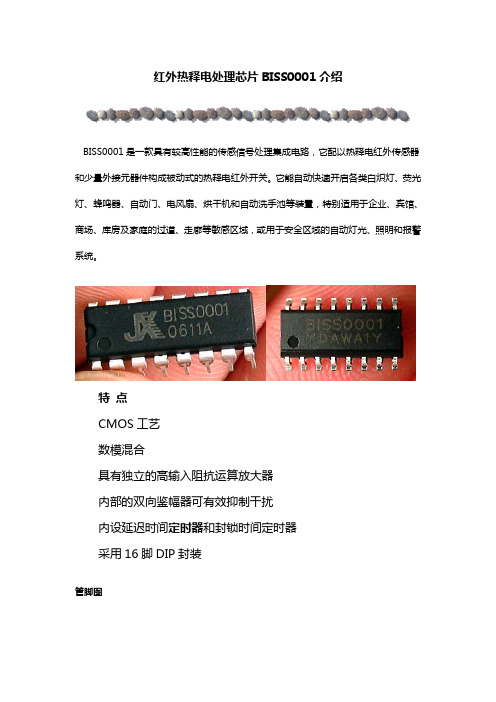
红外热释电处理芯片BISS0001介绍BISS0001是一款具有较高性能的传感信号处理集成电路,它配以热释电红外传感器和少量外接元器件构成被动式的热释电红外开关。
它能自动快速开启各类白炽灯、荧光灯、蜂鸣器、自动门、电风扇、烘干机和自动洗手池等装置,特别适用于企业、宾馆、商场、库房及家庭的过道、走廊等敏感区域,或用于安全区域的自动灯光、照明和报警系统。
特点CMOS工艺数模混合具有独立的高输入阻抗运算放大器内部的双向鉴幅器可有效抑制干扰内设延迟时间定时器和封锁时间定时器采用16脚DIP封装管脚图管脚说明引脚名称I/O功能说明1 A I可重复触发和不可重复触发选择端。
当A为“1”时,允许重复触发;反之,不可重复触发2 VO O 控制信号输出端。
由VS的上跳前沿触发,使Vo输出从低电平跳变到高电平时视为有效触发。
在输出延迟时间Tx之外和无VS的上跳变时,Vo保持低电平状态。
3 RR1 -- 输出延迟时间Tx的调节端4 RC1 -- 输出延迟时间Tx的调节端5 RC2 -- 触发封锁时间Ti的调节端6 RR2 -- 触发封锁时间Ti的调节端7 VSS -- 工作电源负端8 VRF I 参考电压及复位输入端。
通常接VDD,当接“0”时可使定时器复位9 VC I 触发禁止端。
当VcVR时允许触发(VR≈0.2VDD)10 IB -- 运算放大器偏置电流设置端11 VDD -- 工作电源正端2OU12O 第二级运算放大器的输出端T13 2IN- I 第二级运算放大器的反相输入端14 1IN+ I 第一级运算放大器的同相输入端15 1IN- I 第一级运算放大器的反相输入端1OU16O 第一级运算放大器的输出端T工作原理BISS0001是由运算放大器、电压比较器、状态控制器、延迟时间定时器以及封锁时间定时器等构成的数模混合专用集成电路。
以下图所示的不可重复触发工作方式下的波形,来说明其工作过程。
不可重复触发工作方式下的波形。
EDF1BS中文资料(vishay)中文数据手册「EasyDatasheet - 矽搜」
2
12-Jul-05
芯片中文手册,看全文,戳
EDF1AS直通EDF1DS
30
TJ = 25 °C
25
F = 1.0兆赫
Vsig = 50mVp-p
20
15 Juncti1o0n Capacitance (pF)
5.0
0
0.1
1
10
Reverse Voltage (V)
图5.典型结电容每支架
100 200
以英寸封装外形尺寸(毫米)
0.205 (5.2) 0.195 (5.0)
机箱样式 DFS
0.047 (1.20) 0.040 (1.02)
安装焊盘拉 YOUT
0.047最小 (1.20最小)
0.335 (8.51) 0.320 (8.13) 45o
0.130 (3.3) 0.013 (0.330) 0.120 (3.05) 0.009 (0.241)
1,000
100
TJ = 125 °C
10
Instanta1neous Reverse Leakage Current (µA)
TJ = 25 °C
0.1
0
20
40
60
80
100
Percent of Rated PeakReverse Voltage (%)
图4.典型反向漏电特性每支架
文件编号88578
和电信应用
~
机械数据
Case: DFS
环氧符合UL-94V-0阻燃等级
终端:
雾锡电镀(E3后缀)线索,可焊
每个能J-STD-002B和JESD22-B102D
极性: 对人体标示
最大额定值
斑马ZebraZPLII指令集---中文说明解释
斑马ZebraZPLII指令集---中⽂说明解释我们最常⽤的斑马(Zebra)条码打印机,应⽤ZPLII命令来控制打印,说明书中有每条指令的详细说明及相关⽰例,下⾯是各指令的中⽂释义:^A 对Zebra内置点阵字体缩放 ^A(可缩放/点阵字体)命令⽤于内置的True Type字体。
可缩放字体(也可以认为是平滑⽮量字体)能够以点为单位来对横向、纵向进⾏扩展。
点阵字体由点阵象素组成,通常⾼度⾼度⼤于宽度。
内置的的缩放字体(A0=CG Triumvirate Bold Condensed)默认为不旋转,15点⾼,12点宽。
打印机将从^A命令得到字体的旋转⽅向、宽度、⾼度等参数。
^A命令的格式: ^Af,o,h,w^A=缩放/点阵字体f=字体名默认值:0(CG Triumvirate Bold Condensed)其他值:A-Z,0-9(打印机的任何字体,包括下载字体,EPROM中储存的,当然这些字体必须⽤^CW来定义为A-Z,0-9)0=字体⽅向默认值:^FW默认值或上⼀个^FW的值。
其他值:N = 正常(Normal)R = 顺时针旋转90度(Roated)I = 顺时针旋转180度(Inverted)B = 顺时针旋转270度 (Bottom)h=字符⾼度曲线字体:默认值:15点或上⼀次^CF的值。
可接受的10-1500点值:点阵字体:默认值:指定点阵字体的标准⾼度其他值:标准⾼度⾼度的整数倍,2-10。
w=字符宽度曲线字体:默认值:12点或上⼀次^CV的值,也可以显⽰为0可接受的10-1500点值:点阵字体:默认值:指定点阵字体的标准宽度其他值:标准⾼度⾼度的整数倍,2-10。
^A@ 使⽤字体名来调⽤字体 ^A@(使⽤字体名来调⽤字体)命令使⽤字体的全名,来调⽤字体⽰例:^XAA@N,25,25,B:CYRILLIC.FNT^FO100,20^FS^XAA@N,25,25,B:CYRILLIC.FNT^FO100,20^FS^FDThis is a test.^FS^A@N,50,50^FO200,40^FS^FDThis string uses the B:Cyrillic.FNT^FS^XZ 第⼀⾏命令将查找字体卡/后备电池RAM(B:)中的“Cyrillic.FNT”字体,当字体找到后,命令将继续定义字符的⽅向,⼤⼩,然后在标签上打印字段数据“This is a test.” ⼀旦^A命令定义⼀个新字体名时。
艺利磁选机说明书(中文)

ERIEZ MAGNETICS艺利湿式磁选机安装调试、操作和维护保养手册艺利公司湿式磁选机安装调试,运行和维护保养手册本安装调试,运行和维护保养手册适用于按照统一质量标准生产的所有艺利分公司制造的湿式磁选机索引INDEX承诺和保证资料WARRANTY AND GUARANTEE DATA:标准零部件供应商资料VENDOR DATA磁选机说明书OPERATIONAL MANUAL1. 引言INTRODUCTION2. 概述GENERAL DESCRIPTION3. 安装INSTALLATION3.1 运输和储藏TRANSPORT AND STORAGE3.2 安装前预检PRE-COMMISSIONING CHECKS3.3 设备调整ADJUSTMENTS4. 操作OPERATION4.1 磁系调整MAGNET ADJUSTMENT4.2 给料和选别区的调整FEED AND SQUEEZE-PAN ADJUSTMENT4.3 液位和溢流的调整WATER LEVEL AND OVERFLOW ADJUSTMENT4.4 刮板的调整RUBBER WIPER ADJUSTMENT4.5 槽体类型TANK STYLE5. 维护保养MAINTENANCE5.1 发现并处理故障TROUBLESHOOTING5.2 润滑LUBRICATION6. 可更换的外层耐磨筒皮REPLACEABLE WEAR WRAP7. 推荐的备品配件明细表RECOMMENDED SPARE PARTS LIST8. 电机减速器GEAR MOTOR所有由艺利公司生产的磁力设备,如果是按照要求的方式和目的进行正确的安装和使用的话,艺利公司保证该设备可以履行合同中所述的设计要求。
另外,每一台艺利产品按照艺利标准都有为期一年的质量担保。
为维护买方的利益,艺利公司担保:●所有艺利公司生产的设备都是选用最好的原材料和最先进的制造工艺;●在货物发运之后的一年内,对于设备所产生的缺陷,只要是经过艺利公司或经授权的当地代理的检查,确认设备是买方所使用并且是被正确使用的,艺利公司都将免费对零部件进行修理或更换。
《鹿特丹规则》的巨人之踵:承运人责任期间的强制性问题研究
用 的“ 巨人 之踵 ” 承运人 责任 期 间 的强 制性 问题 。 : 与
近 1 3年 的立法 热情 相 对 照 的 , 国际社 会 异 常谨 慎 是
收 稿 日期 : 0 1 0 — 6 2 1 - 6 1
强 制性 问题 却鲜 有提 及 。本 文 以承运 人 责任 期 间的
基 金 项 目 : 育部 人 文 社 科 一 般 项 目《 特 丹 规 则 研 究 : 度 创 新 与借 鉴 》1 Y C 2 1 7 , 海 市 政 府 决 策 咨 询 研 究 项 教 鹿 制 ( 0 J 8 0 4 )上
则” 为篇名 。如 果计 入 对“ 输 法草 案 ” 运 的研 究 , 这一
国 际货 物 运 输合 同公 约 》 又 称 《 特 丹规 则 》 都 堪 ( 鹿 )
称近 年来 国际统一 实体 法 公约 中为数 不多 的 “ 巨人 ”
之一 。《 鹿特 丹规 则 》 的立 法者 试 图全 面实 现 海上 货
第2 2卷
第 3期
中 国 海 商 法 年 刊
Annu lo i a ii e La a f Ch na M r tm w
V oI 2 N o.3 .2
Se p. 20 11
21 0 1年 9月
章 博 .《 特 丹 规 则 》 巨 人 之 踵 : 运 人 责 任 期 间 的 强 制 性 问题 研 究 E] 中 国海 商 法 年 刊 ,0 1 2 ( ) 1—0 鹿 的 承 J. 2 1 ,2 3 :52
c r i r’ e po i lt r o a r e S r s ns bii y pe i d
ZH A N G Bo
( c o lo w ,S a g a a i me Un v r i S h o fLa h n h iM rt ie st i y,S a g a 2 1 0 ,Ch n ) hn hi 036 ia Ab t a t Th o u s r a u e o a r r S r s o sb l y p ro y b h e b t ce f r t e Ro t r a Ru e s r c : e c mp lo y n t r fc r i ’ e p n i i t e i d ma e t e k y o s a l o h te d m ls e i t i a l a e e fc .Th o c p h r o a o g b e s n e s o d a d t en w r v so s u d rt e Ro tr a o fn l t k fe t y e c n e tt e e f s l n e n miu d r t o n h e p o ii n n e h t d m h e
SBL(上料机)
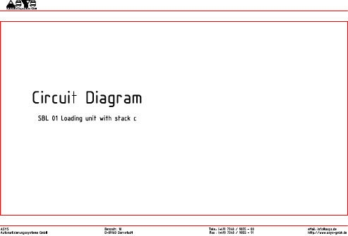
2 Klemmenplan/terminalblock diagram SBL 01 Loading unit with stack c
+A-X1.0,+A-X1.1,+A-X1.2,+A-X1.3 +A-X1.4,+A-X1.6 1/2 .......... 1 2/2 .......... 2
Order-No.:
ASYS Automatisierungssysteme GmbH
Benzstr. 10 D-89160 Dornstadt
Tele.: (+49) 7348 / 9855 - 00 Fax : (+49) 7348 / 9855 - 91
eMail: info@asys.de http://www.asys-gmbh.de
1 Stromlaufplan/wiring diagram SBL 01 Loading unit with stack c
Stromversorgung/AC power supply Stromversorgung/AC power supply Not-Halt/emergency stop Interlock/interlock Interlock/interlock Signalleuchten/signal lights Not-End Z-Achse/safety limit Z-axis Kontrolle/check Aktor-Sensor-Box Bänder/gripper conveyors Aktor-Sensor-Box 2/gripper 2 Bandsensoren/sensors conveyor Bänder/conveyors Aktor-Sensor-Box Greifer/gripper actuator-sen Vakuumkopf/vakuum-head Greifer/gripper Y-Achse Spur 1/Y-axis track 1 Y-Achse/Y-axis 1/25 .......... 1.0 2/25 .......... 1.1 3/25 .......... 2.0 4/25 .......... 2.1 5/25 .......... 2.2 6/25 .......... 3.0 7/25 .......... 3.1 8/25 .......... 3.3 9/25 .......... 3.4 10/25 .......... 3.7 11/25 .......... 4.0 12/25 .......... 4.3 13/25 .......... 5.1 14/25 .......... 5.3 15/25 .......... 5.5 16/25 .......... 7.1 17/25 .......... 7.2 Z-Achse/Z-axis Z-Achse/Z-axis Schnittstellenmodul/interfacemodule Anschlussbelegung/connecting pins Berghof Bedienteil/control panel Schnittstellenkabel/interfacecable Schnittstellenkabel/interfacecable Übersichtsplan/Layout 18/25 .......... 7.3 19/25 .......... 7.4 20/25 .......... 10.0 21/25 .......... 11.0 22/25 .......... 12.0 23/25 .......... 14.0 24/25 .......... 14.2 25/25 .......... 15.3
宏控 SBL 系列电容式靶式流量计 说明书

1、零点设置............................................................................................................................................ 11 2、累积流量清零..................................................................................................................................... 11 3、参数设置及保存................................................................................................................................. 11 4、参数操作............................................................................................................................................ 12
电话:0592-7160574 传真:0592-3776651
地址:厦门市思明区塔埔东路 165 号
1ZC24中文资料

TOSHIBA ZENER DIODE SILICON DIFFUSED TYPE1ZC12~1ZC120CONSTANT VOLTAGE REGULATION TELEPHONE, PRINTER USESl Average Power Dissipation : P = 1.0W l Zener Voltage : V Z = 12~120 Vl Tolerance of Zener Voltage (V Z ) : ±10%l Plastic Mold PackageMAXIMUM RATINGS (Ta=25°C)CHARACTERISTIC SYMBOL RATINGUNITPower Dissipation P 1.0WJunction Temperature T j −40~150 °C Storage Temperature RangeT stg−40~150 °CMARKINGJEDEC ―EIAJ ― TOSHIBA 3−3F2A Weight: 0.18g (Typ.)Unit: mm TENTATIVEELECTRICAL CHARACTERISTICS (Ta=25°C)ZENER CHARACTERISTICSFORWARDVOLTAGEREVERSE CURRENT ZENER VOLTAGE V Z (V) ZENER IMPEDANCE r d (Ω)TEMPERATURE COEFFICIENTOF ZENER VOLTAGEαT (mV / °C) V F (V) I R (µA) TYPEMIN. TYP. MAX. MAX. MEASURE-MENT CURRENT I Z (mA)TYP.MAX.MAX. MEASURE-MENTCURRENT I F (A) MAXMEASURE-MENT VOLTAGE V R (V)1ZC12 10.8 12 13.2 30 10 8 13 1.2 0.2 10 8.0 1ZC13 11.7 13 14.3 30 10 9 14 1.2 0.2 10 9.0 1ZC15 13.5 15 16.5 30 10 11 17 1.2 0.2 10 10.0 1ZC16 14.4 16 17.6 30 10 12 19 1.2 0.2 10 11.0 1ZC18 16.2 18 19.8 30 10 14 23 1.2 0.2 10 13.0 1ZC20 18.0 20 22.0 30 10 16 26 1.2 0.2 10 14.0 1ZC22 19.8 22 24.2 30 10 18 28 1.2 0.2 10 16.0 1ZC24 21.6 24 26.4 30 10 20 32 1.2 0.2 10 17.0 1ZC27 24.3 27 29.7 30 10 23 36 1.2 0.2 10 19.0 1ZC30 27.0 30 33.0 30 10 25 40 1.2 0.2 10 21.0 1ZC33 29.7 33 36.3 30 10 26 41 1.2 0.2 10 26.4 1ZC36 32.4 36 39.6 30 9 28 45 1.2 0.2 10 28.8 1ZC39 35.1 39 42.9 35 8 30 48 1.2 0.2 10 31.2 1ZC43 38.7 43 47.3 40 7 33 53 1.2 0.2 10 34.4 1ZC47 42.3 47 51.7 65 6 38 60 1.2 0.2 10 37.6 1ZC51 45.9 51 56.1 65 6 43 68 1.2 0.2 10 40.8 1ZC56 50.4 56 61.6 855 48 77 1.2 0.2 10 44.81ZC62 55.8 62 68.2 105 5 53 85 1.2 0.2 10 49.6 1ZC68 61.2 68 74.8 120 4 57 90 1.2 0.2 10 54.4 1ZC75 67.5 75 82.5 150 4 66 104 1.2 0.2 10 60.0 1ZC82 73.8 82 90.2 170 3 71 113 1.2 0.2 10 65.4 1ZC91 81.9 91 100.1 240 3 79 127 1.2 0.2 10 72.8 1ZC100 90.0 100 110.0 300 3 87 138 1.2 0.2 10 80.0 1ZC110 99.0 110 121.0 300 3 96 152 1.2 0.2 10 88.0 1ZC120 108.0 120 132.0 3502.5 106 171 1.2 0.2 10 96.0· TOSHIBA is continually working to improve the quality and reliability of its products. Nevertheless, semiconductor devices in general can malfunction or fail due to their inherent electrical sensitivity and vulnerability to physical stress. It is the responsibility of the buyer, when utilizing TOSHIBA products, to comply with the standards of safety in making a safe design for the entire system, and to avoid situations in which a malfunction or failure of such TOSHIBA products could cause loss of human life, bodily injury or damage to property.In developing your designs, please ensure that TOSHIBA products are used within specified operating ranges as set forth in the most recent TOSHIBA products specifications. Also, please keep in mind the precautions and conditions set forth in the “Handling Guide for Semiconductor Devices,” or “TOSHIBA Semiconductor Reliability Handbook” etc.. · The TOSHIBA products listed in this document are intended for usage in general electronics applications (computer, personal equipment, office equipment, measuring equipment, industrial robotics, domestic appliances, etc.). These TOSHIBA products are neither intended nor warranted for usage in equipment that requires extraordinarily high quality and/or reliability or a malfunction or failure of which may cause loss of human life or bodily injury (“Unintended Usage”). Unintended Usage include atomic energy control instruments, airplane or spaceship instruments, transportation instruments, traffic signal instruments, combustion control instruments, medical instruments, all types of safety devices, etc.. Unintended Usage of TOSHIBA products listed in this document shall be made at the customer’s own risk. · The information contained herein is presented only as a guide for the applications of our products. No responsibility is assumed by TOSHIBA CORPORATION for any infringements of intellectual property or other rights of the third parties which may result from its use. No license is granted by implication or otherwise under any intellectual property or other rights of TOSHIBA CORPORATION or others. · The information contained herein is subject to change without notice.000707EAARESTRICTIONS ON PRODUCT USE。
中美材料对照表
aisi1010化学成分是什么?回答验证码:换一张登录并发表取消回答6132122009-11-26 19:28:11N1在mm去除维度N2取消所有毛刺和锐利N3 AISI 1010年到1020年N4,如果弄翻,供营商去除所有重音N5混合半径N6可允许的投射N7一刹那线N8选择形式general笔记1.是IO714方法2. SI UNITS/TS 1-20-923.对实验装置的标志1-10-05 对实验装置的4. ABBREMATIONS 1-10-01NOTES APPUCABLE呼叫请求1. ISO公尺螺纹对是4218 2.维度在化工或电镀的结束以后申请3.对实验装置1 10DB的表面结束4.基准维度5.表明重大特征FORM :冷成形finish :锌板材向TD 29085删除方面的N1毫米氮气中删除所有毛刺和夏普N3型倡议1010年至1020年N4如果破坏,供应商,以消除所有讲N5混合半径N6投影许可N7闪光线N8替代形式一般债券1 。
是IO714方法2 。
SI单位/温度1-20-923 。
符号的Ts 1-10-054 。
ABBREMATIONS对温度1-10-01附注APPUCABLE的WHERE征稿1 。
国际标准化组织度量线程是42182 。
尺寸后申请化学或电镀整理3 。
表面完成指标1 - 10 -数据库4 。
数据层面5 。
表示显着特点形式:冷成型完成:锌板运输署29085yanlu12009-12-16 21:15:56一﹞奥斯田系不锈钢平时最常看到的304不锈钢即为此类,其标准成分是18%铬加8%镍,即一般所称的18-8不锈钢。
此类不锈钢的特性为无磁性、无法藉由热处理方法来改变其金相组织结构、加工性佳,又因含合金元素--镍,所以抗蚀性优于只含铬﹝不含镍﹞的另两类不锈钢。
300系不锈钢主要的用途有:一般民生用途如厨房餐具、建材、医疗卫生器材、食品加工用材、交通工具、化工设备及管件、机械设备及零件。
OARS-1Z中文资料
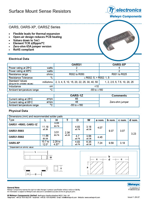
Surface Mount Sense ResistorsOARS1OARS-XPPower rating at 25°C watts 24Power rating at 85ºC watts 12Resistance range ohmsR002 to R050R001 to R025Resistance Tolerance %≤R002:5,>R002:1,5Standard Values(Enquire for unlisted values)milliohms2,3,4,5,10,15,20,22,25,30,40,501,2,2.5,5,7.5,10,20,25InductancenH <10Ambient temperature range°C-55 to +160OARS-1ZCommentsCurrent rating at 25°C amps 65Current rating at 85°Camps 46Ambient temperature range°C-55 to +160Zero-ohm jumperPhysical DataDimensions (mm)and recommended solder pads Type L HT DWa nom.b nom.c nom.d nom.OARS1>R003, OARS-1Z3.05±0.76OARS1-R00311.18±0.384.83±0.763.18±0.384.07OARS1-R00211.56±0.38 3.51±0.76 4.7±0.76 3.56±0.38 4.459.373.07OARS-XP10.7 to 12.0*2.28 to 4.57*2.36±0.254.83±0.766.35±0.387.249.583.18 3.23*Dependent on ohmic valueab dccIssue F .09.07Performance Data (AEC-Q200)OARS1<R004R004to R015>R015OARS-XP <R002R002to R007>R007TCR (-55to 125ºC)ppm/ºC 2404040Thermal Shock∆R%0.750.750.75High Temp.Exposure (125ºC)∆R% 1.750.51Temp.Cycling (-40 to 125ºC)∆R%110.75Operational Life ∆R%211Biased Humidity ∆R%0.750.50.5Mechanical Shock ∆R% 1.511Vibration∆R%111Terminal Strength MeetsJIS-C-6429Solvent Resistance Meets MIL-STD-002Method 215SolderabilityMeets J-STD-002Method BNote:Temperature rise data are given here for typical mountingwidth and substrate type.Also,the open air format responds better to forced air cooling than chip format resistors.For values below 5milliohms allowance should be made for heat generated in the copper tracks themselves.Application-specific guidance is available on request.the square of the current rating.Higher energy limits apply for longer pulses and overloadsIssue F .09.07FlammabilityThe resistor will not burn or emit incandescent particles under any condition of applied temperature or overload.MarkingThe parts are legend marked with ohmic value and tolerance code.Packaging DataDimensions (mm)TypeABCDEFGOARS1, OARS-1Z 4.32±0.0811.7±0.088±0.1OARS-XP-R00111.94±0.1OARS-XP >R0017.21±0.111.56±0.124±0.311.5±0.11.75±0.112±0.14±0.1Ordering ProcedureExample:OARS1at 10milliohms and 5% tolerance on a reel of 1900pieces -PackingOARS11900/reel ITapeOARS-XP 1200/reelStandardFor the zero-ohm link,order OARS-1Z (Pack quantity is 1900/reel)Issue F .09.07。
SBL2060CT中文资料
RqJC
Operating and Storage Temperature Range
Tj, TSTG
SBL 2030CT
30
21
SBL
SBL
SBL
2035CT 2040CT 2045CT
35
40
45
24.5
28
31.5
20
250
0.55 1.0 50 650 2.8
-65 to +150
SBL
SBL
L
3.56 4.83
M
1.14 1.40
N
0.30 0.64
P
2.03 2.92
All Dimensions in mm
Maximum Ratings and Electrical Characteristics @ TA = 25°C unless otherwise specified
Single phase, half wave, 60Hz, resistive or inductive load. For capacitive load, derate current by 20%.
Voltage Drop · For Use in Low Voltage, High Frequency
Inverters, Free Wheeling, and Polarity Protection Applications · Plastic Material: UL Flammability Classification Rating 94V-0
Peak Reverse Current at Rated DC Blocking Voltage
@TC = 25°C @ TC = 100°C
ZLUSBEVAL1Z;中文规格书,Datasheet资料
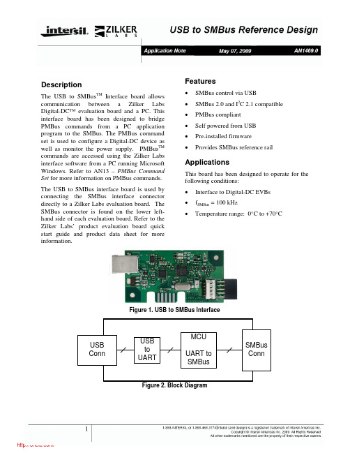
DescriptionThe USB to SMBus TM Interface board allows communication between a Zilker Labs Digital-DC™ evaluation board and a PC. This interface board has been designed to bridge PMBus commands from a PC application program to the SMBus. The PMBus command set is used to configure a Digital-DC device as well as monitor the power supply. PMBus TM commands are accessed using the Zilker Labs interface software from a PC running Microsoft Windows. Refer to AN13 – PMBus Command Set for more information on PMBus commands. The USB to SMBus interface board is used by connecting the SMBus interface connector directly to a Zilker Labs evaluation board. The SMBus connector is found on the lower left-hand side of each evaluation board. Refer to the Zilker Labs’ product evaluation board quick start guide and product data sheet for more information.Features• SMBus control via USB• SMBus 2.0 and I 2C 2.1 compatible • PMBus compliant • Self powered from USB • Pre-installed firmware • Provides SMBus reference railApplicationsThis board has been designed to operate for the following conditions:• Interface to Digital-DC EVBs•f SMBus= 100 kHz• Temperature range: 0°C to +70°CFigure 1. USB to SMBus InterfaceFigure 2. Block DiagramZLUSBREF01SchematicsFigure 1. USB to SMBusZLUSBREF01 Bill of MaterialsItem Quan Reference Value Tol Rating Type PCB Footprint Manufacturer Part Number111C1,C2,C3,C4,C5,C7,C8,C9,C10,C11100n10%10V X7R SM0603KEMET C0603C104K8RACTU22C6,C1310u20% 6.3V SM0603PANASONIC-ECG ECJ-1VB0J106M32C12,C1910n10%25V X7R SM0603PANASONIC-ECG ECJ-1VB1E103K42C14,C1547p5%50V COG SM0603TDK C1608C0G1H470J52C16,C1722p5%50V COG SM0603MURATA GRM1885C1H220JA01D 62D1,D2ESDA6V1-4BC6 6.1V, 80W SOT23_6L ST MICRO ESDA6V1-4BC671D3BAT54XV2T1OS200mA SOD-523ON SEMI BAT54XV2T1OS81D4LED Green20mA CLR SM0805_DIO_1C2A CHICAGO MINI CMD17-21VGC91D5LED Red20mA CLR SM0805_DIO_1C2A CHICAGO MINI CMD17-21VRC101FB140 OHM 1.5A MLF SM0805STEWARD MI0805K400R-00 MI0805K400R-01111J1USB TYPE B USB\B MOLEX67068-0000121J2HEADER 5X2HDRF5DUALRA100X100SAMTEC SSQ-105-02-T-D-RA 131J3 5 PIN SN HDR5LK100AMP640456-5141J42mm, 5 PIN SN SIP_5P_2.0MM Sullins PRPN051PAEN151J6 2 PIN SN SIP2/100TYCO644456-2163Q1,Q2,Q3FDG6301N25V DUAL N-CH SC70-6FAIRCHILD SEMI FDG6301N171R10THK FILM SM0805YAGEO RC0805JR-070RL 181R24705%63mW THK FILM SM0402ROHM MCRMZPF4700192R3,R510k1%100mW THK FILM SM0603ROHM MCR03EZPFX1002 205R4,R6,R20,R2610k1%63mW THK FILM SM0402YAGEO RC0402FR-0710KL 213R7,R8,R9 2.49k1%100mW THK FILM SM0603ROHM MCR03EZPFX2491 221R101M1%63mW THK FILM SM0402ROHM MCR01MZPF1004 232R11,R13275%63mW THK FILM SM0402YAGEO RC0402JR-0727RL 241R12 1.50k1%63mW THK FILM SM0402YAGEO RC0402FR-071K5L 254R17,R18,R24,R252211%63mW THK FILM SM0402YAGEO RC0402FR-07221L 261R21 4.75k0.0163mW THK FILM SM0402PANASONIC-ECG ERJ-2RKF4751X 271R23 2.49k0.0163mW THK FILM SM0402PANASONIC-ECG ERJ-2RKF2491X 281U1ATMega32L-8MC MCU MLF44_7X7_DP ATMEL ATMEGA32L-8MC 291U2FT232BQ TQFP32/.8P/9X9FTDI FT232BQ301U3MIC2920A-3.3WS400mA SOT223_1234_REV1MICREL MIC2920A-3.3WS TR 311U493C46-TSSOP 1.8 - 5.5V93C46TSSOP8/.65P/6.4ATMEL AT93C46-10TI-1.8 321Y16MHz RESONATOR0.01COMM CERALOCK MURATA CSTCR6M00G53-R0331Y28MHz Crystal,CL = 18pF30ppm CSM-7X575CT ECS INC ECS-80-18-5PNI TP1,TP2,TP3,TP4T POINT S TP_020HNI R15,R16NI1%SM0402NI J5AVRISP_10PinConn HDR10DUAL100X100NI R1410k1%63mW THK FILM SM0402YAGEO RC0402FR-0710KL NI C18100n0.110V X7R SM0603KEMET C0603C104K8RACTU NI =Not InstalledZLUSBREF01References[1]AN13 – PMBus Command Set, Zilker Labs, Inc., 2007.[2]ZL2005 Data Sheet, Zilker Labs, Inc., 2006.[3]ZL2105 Data Sheet, Zilker Labs, Inc., 2007.[4]ZL2005EV1 Quick Start Guide, Zilker Labs, Inc., 2006.[5]ZL2105EV1 Quick Start Guide, Zilker Labs, Inc., 2006.Ordering InformationOrderableDescription Part NumberZLUSBREF01 USB to SMBus InterfaceRevision HistoryDate Rev. #3/27/2007 0.5 Preliminary Release4/26/2007 1.0 Final ReleaseZLUSBREF01 NOTESZLUSBREF01Zilker Labs, Inc.4301 Westbank DriveBuilding A-100Austin, TX 78746Tel: 512-382-8300Fax: 512-382-8329© 2007, Zilker Labs, Inc. All rights reserved. Zilker Labs, Digital-DC and the Zilker Labs Logo are trademarks of Zilker Labs, Inc. All other products or brand names mentioned herein are trademarks of their respective hold-ers.This document contains information on a reference design. Pricing, specifications and availability are subject to change without notice. Please see for updated information. This product is not intended for use in connection with any high-risk activity, including without limitation, air travel, life critical medical operations, nuclear facilities or equipment, or the like.The reference designs contained in this document are for reference and example purposes only. THE REFER-ENCE DESIGNS ARE PROVIDED "AS IS" AND "WITH ALL FAULTS" AND ZILKER LABS DISCLAIMS ALL WARRANTIES, WHETHER EXPRESS OR IMPLIED. ZILKER LABS SHALL NOT BE LIABLE FOR ANY DAMAGES, WHETHER DIRECT, INDIRECT, CONSEQUENTIAL (INCLUDING LOSS OF PROF-ITS), OR OTHERWISE, RESULTING FROM THE REFERENCE DESIGNS OR ANY USE THEREOF. Any use of such reference designs is at your own risk and you agree to indemnify Zilker Labs for any damages result-ing from such use.分销商库存信息: INTERSIL ZLUSBEVAL1Z。
5551 晶体管芯片说明书

参数符号
符号说明
ICBO
集电极—基极截止电流
IEBO
发射极—基极截止电流
hFE
直流电流增益
VCE(sat) 集电极—发射极饱和电压
VBE(sat) 基极—发射极饱和电压
BVCBO BVCEO BVEBO fT
集电极—基极击穿电压 集电极—发射极击穿电压 发射极—基极击穿电压 特征频率
最小值 典型值 最大值 单 位 测 试 条 件
0.05 µA VCB=120V,IE=0
0.05 µA VEB=4V,IC=0
80
VCE=5V,IC=1mA
80
280
VCE=5V,IC=10mA
30
VCE=5V,IC=50mA
0.15
V IC=10mA,IB=1mA
0.2
V IC=50mA,IB=5mA
1
V IC=10mA,IB=1mA
1
V IC=50mA,IB=5mA
180
V IC=100µA,IE=0
160
V IC=1mA,IB=0
6
V IE=10µA,IC=0
100
300 MHz VCE=10V,IC=10mA图
█ 极限值(Ta=25℃)(封装形式:TO-92)
Tstg——贮存温度…………………………………… -55~150℃ Tj——结温…………………………………………………150℃ PC——集电极耗散功率…………………………………625mW VCBO——集电极—基极电压………………………………180V VCEO——集电极—发射极电压……………………………160V VEBO——发射极—基极电压…………………………………6V IC——集电极电流…………………………………………600mA
凌特公司基准芯片参数
凌特公司基准芯片参数表基准输出形式初始精度温飘最低压差静态电流或最低旁路电流温度分档封装单位V % ppm/°C V uALT6650CS50.4 串联0.75 30 .1 11uA 0°C ~ 70°C SOT-23LT6650HS50.4 串联 1.5 30 .1 11uA -40°C ~ 125°C SOT-23LT6650IS50.4 串联 1 30 .1 11uA -40°C ~ 85°C SOT-23LTC1440 1.182 并联 1 55.5 并联 2 0°C ~ 70°C, -40°C ~ 85°C MS-8, SO-8, DIP-8, DFN-8LTC1442 1.182 并联 1 55.5 并联 3.5 0°C ~ 70°C, -40°C ~ 85°C SO-8, DIP-8LTC1443 1.182 并联 1 44.4 并联 5.5 0°C ~ 70°C, -40°C ~ 85°C DIP-16, SO-16, DFN-16LTC1540 1.182 并联 2.2 62.5 并联0.3 MS-8, SO-8, DFN-8LTC1842 1.182 并联 1 55.5 并联 3.5 0°C ~ 70°C, -40°C ~ 85°C SO-8LTC1843 1.182 并联 1 55.5 并联 3.5 0°C ~ 70°C, -40°C ~ 85°C SO-8LTC1541 1.2 并联 1.25 62.5 并联 5 0°C ~ 70°C, -40°C ~ 85°C MS-8, SO-8, DFN-8LTC1998 1.2 并联0.6 71 并联 3.5 0°C ~ 70°C, -40°C ~ 85°C SOT-23LTC1444 1.221 并联 1 44.4 并联 5.5 0°C ~ 70°C, -40°C ~ 85°C DIP-16, SO-16LTC1445 1.221 并联 1 44.4 并联 5.5 0°C ~ 70°C, -40°C ~ 85°C DIP-16, SO-16, DFN-16LT1034BCZ-1.2 1.225 并联 1.2 20 并联10 0°C ~ 70°C TO-92LT1034BIZ-1.2 1.225 并联 1.2 20 并联10 -40°C ~ 85°C TO-92LT1034CS8-1.2 1.225 并联 1.2 40 并联10 0°C ~ 70°C SO-8LT1034CZ-1.2 1.225 并联 1.2 40 并联10 0°C ~ 70°C TO-92LT1034IS8-1.2 1.225 并联 1.2 40 并联10 -40°C ~ 85°C SO-8LT1034IZ-1.2 1.225 并联 1.2 40 并联10 -40°C ~ 85°C TO-921LT1004IS8-1.2 1.235 并联0.8 20 并联8 -40°C ~ 85°C SO-8LT1004IZ-1.2 1.235 并联0.3 20 并联8 -40°C ~ 85°C TO-92LT1389ACS8-1.25 1.25 并联0.05 10 并联0.6 0°C ~ 70°C SO-8LT1389BCS8-1.25 1.25 并联0.05 20 并联0.6 0°C ~ 70°C SO-8LT1634ACS8-1.25 1.25 并联0.05 10 并联7 0°C ~ 70°C SO-8LT1634AIS8-1.25 1.25 并联0.05 10 并联7 -40°C ~ 85°C SO-8LT1634BCMS8-1.25 1.25 并联0.05 25 并联7 0°C ~ 70°C MS-8LT1634BCS8-1.25 1.25 并联0.05 25 并联7 0°C ~ 70°C SO-8LT1634BIS8-1.25 1.25 并联0.05 25 并联7 -40°C ~ 85°C SO-8LT1634CCZ-1.25 1.25 并联0.2 25 并联7 0°C ~ 70°C TO-92LT1790ACS6-1.25 1.25 串联0.05 10 .1 35 0°C ~ 70°C SOT-23LT1790AIS6-1.25 1.25 串联0.05 10 .1 35 -40°C ~ 85°C SOT-23LT1790BCS6-1.25 1.25 串联0.1 25 .1 35 0°C ~ 70°C SOT-23LT1790BIS6-1.25 1.25 串联0.1 25 .1 35 -40°C ~ 85°C SOT-23LTC6652AHMS8-1.25 1.25 串联0.05 5 .3 350 -40°C ~ 125°C MS-8LTC6652BHMS8-1.25 1.25 串联0.1 10 .3 350 -40°C ~ 125°C MS-8LTC6655BHMS8-1.25 1.25 串联0.025 2 .5 5000 -40°C ~ 125°C MS-8LTC6655CHMS8-1.25 1.25 串联0.05 5 .5 5000 -40°C ~ 125°C MS-8LT1790ACS6-2.048 2.048 串联0.05 10 .1 35 0°C ~ 70°C SOT-23LT1790AIS6-2.048 2.048 串联0.05 10 .1 35 -40°C ~ 85°C SOT-23LT1790BCS6-2.048 2.048 串联0.1 25 .1 35 0°C ~ 70°C SOT-23LT1790BIS6-2.048 2.048 串联0.1 25 .1 35 -40°C ~ 85°C SOT-23LTC6652AHMS8-2.0482.048 串联0.05 5 .3 350 -40°C ~ 125°C MS-8LTC6652BHMS8-2.0482.048 串联0.1 10 .3 350 -40°C ~ 125°C MS-8LTC6655BHMS8-2.0482.048 串联0.025 2 .5 5000 -40°C ~ 125°C MS-8LTC6655CHMS8-2.0482.048 串联0.05 5 .5 5000 -40°C ~ 125°C MS-8LT1004CS8-2.5 2.5 并联0.8 20 并联12 0°C ~ 70°C SO-82LT1004IZ-2.5 2.5 并联0.8 20 并联12 -40°C ~ 85°C TO-92LT1009CMS8 2.5 并联0.2 25 并联400 0°C ~ 70°C MS-8LT1009CZ 2.5 并联0.2 25 并联400 0°C ~ 70°C TO-92LT1009IS8 2.5 并联0.4 35 并联400 -40°C ~ 85°C SO-8LT1009IZ 2.5 并联0.2 35 并联400 -40°C ~ 85°C TO-92LT1009S8 2.5 并联0.4 25 并联400 0°C ~ 70°C SO-8LT1019ACN8-2.5 2.5 串联0.05 5 1.1 650 0°C ~ 70°C DIP-8LT1019ACS8-2.5 2.5 串联0.05 5 1.1 650 0°C ~ 70°C SO-8LT1019AIS8-2.5 2.5 串联0.05 10 1.1 650 -40°C ~ 85°C SO-8LT1019CN8-2.5 2.5 串联0.2 20 1.1 650 0°C ~ 70°C DIP-8LT1019CS8-2.5 2.5 串联0.2 20 1.1 650 0°C ~70°C SO-8LT1019IN8-2.5 2.5 串联0.2 20 1.1 650 -40°C ~ 85°C DIP-8LT1019IS8-2.5 2.5 串联0.2 20 1.1 650 -40°C ~ 85°C SO-8LT1034BCZ-2.5 2.5 并联 1.6 20 并联15 0°C ~ 70°C TO-92LT1034BIZ-2.5 2.5 并联 1.6 20 并联15 -40°C ~ 85°C TO-92LT1034CS8-2.5 2.5 并联 1.6 40 并联15 0°C ~ 70°C SO-8LT1034CZ-2.5 2.5 并联 1.6 40 并联15 0°C ~ 70°C TO-92LT1034IS8-2.5 2.5 并联 1.6 40 并联15 -40°C ~ 85°C SO-8LT1034IZ-2.5 2.5 并联 1.6 40 并联15 -40°C ~ 85°C TO-92LT1389BCS8-2.5 2.5 并联0.05 20 并联0.6 0°C ~ 70°C SO-8LT1460ACN8-2.5 2.5 串联0.075 10 .9 100 0°C ~ 70°C DIP-8LT1460ACS8-2.5 2.5 串联0.075 10 .9 100 0°C ~ 70°C SO-8LT1460BIN8-2.5 2.5 串联0.1 10 .9 100 -40°C ~ 85°C DIP-8LT1460BIS8-2.5 2.5 串联0.1 10 .9 100 -40°C ~ 85°C SO-8LT1460CCMS8-2.5 2.5 串联0.1 15 .9 100 0°C ~ 70°C MS-8LT1460DCN8-2.5 2.5 串联0.1 20 .9 100 0°C ~ 70°C DIP-8LT1460DCS8-2.5 2.5 串联0.1 20 .9 100 0°C ~ 70°C SO-83LT1460EIN8-2.5 2.5 串联0.125 20 .9 100 -40°C ~ 85°C DIP-8LT1460EIS8-2.5 2.5 串联0.125 20 .9 100 -40°C ~ 85°C SO-8LT1460FCMS8-2.5 2.5 串联0.15 25 .9 100 0°C ~ 70°C MS-8LT1460GCZ-2.5 2.5 串联0.25 25 .9 100 0°C ~ 70°C TO-92LT1460GIZ-2.5 2.5 串联0.25 25 .9 100 -40°C ~ 85°C TO-92LT1460HCS3-2.5 2.5 串联0.5 20 .9 100 0°C ~ 70°C SOT-23LT1460JCS3-2.5 2.5 串联0.4 20 .9 100 0°C ~ 70°C SOT-23LT1460KCS3-2.5 2.5 串联0.5 50 .9 100 0°C ~ 70°C SOT-23LT1460LHS8-2.5 2.5 串联0.2 25 .9 100 -40°C ~ 125°C SO-8LT1460MHS8-2.5 2.5 串联0.2 50 .9 100 -40°C ~ 125°C SO-8LT1461ACS8-2.5 2.5 串联0.04 3 .3 35 0°C ~ 70°C SO-8LT1461AIS8-2.5 2.5 串联0.04 3 .3 35 -40°C ~ 85°C SO-8LT1461BCS8-2.5 2.5 串联0.06 7 .3 35 0°C ~ 70°C SO-8LT1461BIS8-2.5 2.5 串联0.06 7 .3 35 -40°C ~ 85°C SO-8LT1461CCS8-2.5 2.5 串联0.1 12 .3 35 0°C ~ 70°C SO-8LT1461CIS8-2.5 2.5 串联0.1 12 .3 35 -40°C ~ 85°C SO-8LT1461DHS8-2.5 2.5 串联0.15 20 .3 35 -40°C ~ 125°C SO-8LT1634ACS8-2.5 2.5 并联0.05 10 并联7 0°C ~ 70°C SO-8LT1634AIS8-2.5 2.5 并联0.05 25 并联7 -40°C ~ 85°C SO-8LT1634BCMS8-2.5 2.5 并联0.05 25 并联7 0°C ~ 70°C MS-8LT1634BCS8-2.5 2.5 并联0.05 25 并联7 0°C ~ 70°C SO-8LT1634BIS8-2.5 2.5 并联0.05 25 并联7 -40°C ~ 85°C SO-8LT1634CCZ-2.5 2.5 并联0.2 25 并联7 0°C ~ 70°C TO-92LT1790ACS6-2.5 2.5 串联0.05 10 .1 35 0°C ~ 70°C SOT-23LT1790AIS6-2.5 2.5 串联0.05 10 .1 35 -40°C ~ 85°C SOT-23LT1790BCS6-2.5 2.5 串联0.1 25 .1 35 0°C ~ 70°C SOT-23LT1790BIS6-2.5 2.5 串联0.1 25 .1 35 -40°C ~ 85°C SOT-23LT6654AHS6-2.5 2.5 串联0.05 3 .055 350 -40°C ~ 85°C SOT-23LT6654AMPS6-2.5 2.5 串联0.05 3 .055 350 -55°C ~ 125°C SOT-234LT6654BHS6-2.5 2.5 串联0.1 6 .055 350 -55°C ~ 125°C SOT-23LT6654BMPS6-2.5 2.5 串联0.1 6 .055 350 -40°C ~ 85°C SOT-23LT6656ACS6-2.5 2.5 串联0.05 10 .5 0.85 0°C ~ 70°C SOT-23LT6656AIS6-2.5 2.5 串联0.05 10 .5 0.85 -40°C ~ 85°C SOT-23LT6656BCS6-2.5 2.5 串联0.1 20 .5 0.85 0°C ~ 70°C SOT-23LT6656BIS6-2.5 2.5 串联0.1 20 .5 0.85 -40°C ~ 85°C SOT-23LT6660HCDC-2.5 2.5 串联0.2 20 .9 115 0°C ~ 70°C DFN-3LT6660JCDC-2.5 2.5 串联0.4 20 .9 115 0°C ~ 70°C DFN-3LT6660KCDC-2.5 2.5 串联0.5 50 .9 115 0°C ~ 70°C DFN-3LTC1258CMS8-2.5 2.5 串联0.21 60 .1 4 0°C ~ 70°C MS-8LTC1258CS8-2.5 2.5 串联0.15 40 .1 4 0°C ~ 70°C SO-8LTC1798CS8-2.5 2.5 串联0.15 15 .1 4 0°C ~ 70°C SO-8LTC6652AHMS8-2.5 2.5 串联0.05 5 .3 350 -40°C ~ 125°C MS-8LTC6652BHMS8-2.5 2.5 串联0.1 10 .3 350 -40°C ~ 125°C MS-8LTC6655BHMS8-2.5 2.5 串联0.025 2 .5 5000 -40°C ~ 125°C MS-8LTC6655CHMS8-2.5 2.5 串联0.05 5 .5 5000 -40°C ~ 125°C MS-8LT1460HCS3-3 3 串联0.2 20 .9 145 0°C ~ 70°C SOT-23LT1460JCS3-3 3 串联0.4 20 .9 145 0°C ~ 70°C SOT-23LT1460KCS3-3 3 串联0.5 50 .9 145 0°C ~ 70°C SOT-23LT1461ACS8-3 3 串联0.04 3 .3 35 0°C ~ 70°C SO-8LT1461AIS8-3 3 串联0.04 3 .3 35 -40°C ~ 85°C SO-8LT1461BCS8-3 3 串联0.1 10 .3 35 0°C ~ 70°C SO-8LT1461BIS8-3 3 串联0.06 7 .3 35 -40°C ~ 85°C SO-8LT1461CCS8-3 3 串联0.1 12 .3 35 0°C ~ 70°C SO-8LT1461CIS8-3 3 串联0.1 12 .3 35 -40°C ~ 85°C SO-8LT1461DHS8-3 3 串联0.2 20 .3 35 -40°C ~ 125°C SO-8LT1790ACS6-3 3 串联0.05 10 .1 35 0°C ~ 70°C SOT-23LT1790AIS6-3 3 串联0.05 10 .1 35 -40°C ~ 85°C SOT-23LT1790BCS6-3 3 串联0.1 25 .1 35 0°C ~ 70°C SOT-235LT1790BIS6-3 3 串联0.1 25 .1 35 -40°C ~ 85°C SOT-23LT6660HCDC-3 3 串联0.2 20 .9 145 0°C ~ 70°C DFN-3LT6660JCDC-3 3 串联0.4 20 .9 145 0°C ~ 70°C DFN-3LT6660KCDC-3 3 串联0.5 50 .9 145 0°C ~ 70°C DFN-3LTC1258CMS8-3 3 串联0.15 60 .1 4 0°C ~ 70°C MS-8LTC1258CS8-3 3 串联0.15 40 .1 4 0°C ~ 70°C SO-8LTC1798CS8-3 3 串联0.15 15 .1 4 0°C ~ 70°C SO-8LTC6652AHMS8-3 3 串联0.05 5 .3 350 -40°C ~ 125°C MS-8LTC6652BHMS8-3 3 串联0.1 10 .3 350 -40°C ~ 125°C MS-8LTC6655BHMS8-3 3 串联0.025 2 .5 5000 -40°C ~ 125°C MS-8LTC6655CHMS8-3 3 串联0.05 5 .5 5000 -40°C ~ 125°C MS-8LT1460HCS3-3.3 3.3 串联0.2 20 .9 145 0°C ~ 70°C SOT-23LT1460JCS3-3.3 3.3 串联0.4 20 .9 145 0°C ~ 70°C SOT-23LT1460KCS3-3.3 3.3 串联0.5 50 .9 145 0°C ~ 70°C SOT-23LT1461ACS8-3.3 3.3 串联0.04 3 .3 35 0°C ~ 70°C SO-8LT1461AIS8-3.3 3.3 串联0.04 3 .3 35 -40°C ~ 85°C SO-8LT1461BCS8-3.3 3.3 串联0.1 10 .3 35 0°C ~ 70°C SO-8LT1461BIS8-3.3 3.3 串联0.1 10 .3 35 -40°C ~ 85°C SO-8LT1461CCS8-3.3 3.3 串联0.1 12 .3 35 0°C ~ 70°C SO-8LT1461CIS8-3.3 3.3 串联0.1 12 .3 35 -40°C ~ 85°C SO-8LT1461DHS8-3.3 3.3 串联0.2 20 .3 35 -40°C ~ 125°C SO-8LT1790ACS6-3.3 3.3 串联0.05 10 .1 35 0°C ~ 70°C SOT-23LT1790AIS6-3.3 3.3 串联0.05 10 .1 35 -40°C ~ 85°C SOT-23LT1790BCS6-3.3 3.3 串联0.1 25 .1 35 0°C ~ 70°C SOT-23LT1790BIS6-3.3 3.3 串联0.1 25 .1 35 -40°C ~ 85°C SOT-23LT6660HCDC-3.3 3.3 串联0.2 20 .9 145 0°C ~ 70°C DFN-3LT6660JCDC-3.3 3.3 串联0.4 20 .9 145 0°C ~ 70°C DFN-3LT6660KCDC-3.3 3.3 串联0.5 50 .9 145 0°C ~ 70°C DFN-3LTC6652AHMS8-3.3 3.3 串联0.05 5 .3 350 -40°C ~ 125°C MS-86LTC6655BHMS8-3.3 3.3 串联0.025 2 .5 5000 -40°C ~ 125°C MS-8LTC6655CHMS8-3.3 3.3 串联0.05 5 .5 5000 -40°C ~ 125°C MS-8LT1389BCS8-4.096 4.096 并联0.075 50 并联0.6 0°C ~ 70°C SO-8LT1461ACS8-4 4.096 串联0.04 3 .3 35 0°C ~ 70°C SO-8LT1461AIS8-4 4.096 串联0.04 3 .3 35 -40°C ~ 85°C SO-8LT1461BCS8-4 4.096 串联0.06 7 .3 35 0°C ~ 70°C SO-8LT1461BIS8-4 4.096 串联0.1 10 .3 35 -40°C ~ 85°C SO-8LT1461CCS8-4 4.096 串联0.1 12 .3 35 0°C ~ 70°C SO-8LT1461CIS8-4 4.096 串联0.1 12 .3 35 -40°C ~ 85°C SO-8LT1461DHS8-4 4.096 串联0.2 20 .3 35 -40°C ~ 125°C SO-8LT1634ACS8-4.096 4.096 并联0.05 10 并联7 0°C ~ 70°C SO-8LT1634AIS8-4.096 4.096 并联0.05 10 并联7 -40°C ~ 85°C SO-8LT1634BCS8-4.096 4.096 并联0.05 25 并联7 0°C ~ 70°C SO-8LT1634BIS8-4.096 4.096 并联0.05 25 并联7 -40°C ~ 85°C SO-8LT1634CCZ-4.096 4.096 并联0.2 25 并联7 0°C ~ 70°C TO-92LT1790ACS6-4.096 4.096 串联0.05 10 .1 35 0°C ~ 70°C SOT-23LT1790AIS6-4.096 4.096 串联0.05 10 .1 35 -40°C ~ 85°C SOT-23LT1790BCS6-4.096 4.096 串联0.1 25 .1 35 0°C ~ 70°C SOT-23LT1790BIS6-4.096 4.096 串联0.1 25 .1 35 -40°C ~ 85°C SOT-23LTC1258CMS8-4.1 4.096 串联0.15 40 .1 4 0°C ~ 70°C MS-8LTC1258CS8-4.1 4.096 串联0.15 40 .1 4 0°C ~ 70°C SO-8LTC1798CS8-4.1 4.096 串联0.15 15 .1 4 0°C ~ 70°C SO-8LTC6652AHMS8-4.0964.096 串联0.05 5 .3 350 -40°C ~ 125°C MS-8LTC6652BHMS8-4.0964.096 串联0.1 10 .3 350 -40°C ~ 125°C MS-8LTC6655BHMS8-4.0964.096 串联0.025 2 .5 5000 -40°C ~ 125°C MS-8LTC6655CHMS8-4.0964.096 串联0.05 5 .5 5000 -40°C ~ 125°C MS-8LT1019ACN8-4.5 4.5 串联0.05 5 1.1 650 0°C ~ 70°C DIP-8LT1019CN8-4.5 4.5 串联0.2 20 1.1 650 0°C ~ 70°C DIP-87LT1019IN8-4.5 4.5 串联0.2 5 1.1 650 -40°C ~ 85°C DIP-8LT1019ACN8-5 5 串联0.05 5 1.1 650 0°C ~ 70°C DIP-8LT1019ACS8-5 5 串联0.05 3 1.1 650 0°C ~ 70°C SO-8LT1019AIS8-5 5 串联0.05 3 1.1 650 -40°C ~ 85°C SO-8LT1019CN8-5 5 串联0.2 5 1.1 650 0°C ~ 70°C DIP-8LT1019CS8-5 5 串联0.2 20 1.1 650 0°C ~ 70°C SO-8LT1019IN8-5 5 串联0.2 5 1.1 650 -40°C ~ 85°C DIP-8LT1019IS8-5 5 串联0.2 20 1.1 650 -40°C ~ 85°C SO-8LT1021BCH-5 5 串联 1 5 2.2 800 0°C ~ 70°C to-5LT1021BCN8-5 5 串联 1 5 2.2 800 0°C ~ 70°C DIP-8LT1021BMH-5 5 串联 1 5 2.2 800 -55°C ~ 125°C TO-5LT1021CCH-5 5 串联0.05 20 2.2 800 0°C ~ 70°C TO-5LT1021CCN8-5 5 串联0.05 20 2.2 800 0°C ~ 70°C DIP-8LT1021CIN8-5 5 串联0.05 20 2.2 800 -40°C ~ 85°C DIP-8LT1021CMH-5 5 串联0.05 20 2.2 800 -55°C ~ 125°C TO-5LT1021DCN8-5 5 串联 1 20 2.2 800 0°C ~ 70°C DIP-8LT1021DCS8-5 5 串联 1 20 2.2 800 0°C ~ 70°C SO-8LT1021DIN8-5 5 串联 1 20 2.2 800 -40°C ~ 85°C DIP-8LT1027BCN8-5 5 串联0.05 1 3 2200 0°C ~ 70°C DIP-8LT1027CCN8-5 5 串联0.05 2 3 2200 0°C ~ 70°C DIP-8LT1027CCS8-5 5 串联0.05 2 3 2200 0°C ~ 70°C SO-8LT1027DCN8-5 5 串联0.05 2 3 2200 0°C ~ 70°C DIP-8LT1027DCS8-5 5 串联0.05 2 3 2200 0°C ~ 70°C SO-8LT1027ECN8-5 5 串联0.1 3 3 2200 0°C ~ 70°C DIP-8LT1027ECS8-5 5 串联0.1 3 3 2200 0°C ~ 70°C SO-8LT1029ACZ 5 并联0.2 20 并联700 0°C ~ 70°C TO-92LT1029CZ 5 并联 1 34 并联700 0°C ~ 70°C TO-92LT1236ACN8-5 5 串联0.05 2 1 800 0°C ~ 70°C DIP-88LT1236BCN8-5 5 串联0.1 5 1 800 0°C ~ 70°C DIP-8LT1236BCS8-5 5 串联0.1 5 1 800 0°C ~ 70°C SO-8LT1236BIN8-5 5 串联0.1 15 1 800 -40°C ~ 85°C DIP-8LT1236BIS8-5 5 串联0.1 5 1 800 -40°C ~ 85°C SO-8LT1236CCN8-5 5 串联0.1 10 1 800 0°C ~ 70°C DIP-8LT1236CCS8-5 5 串联0.1 10 1 800 0°C ~ 70°C SO-8LT1236CIN8-5 5 串联0.1 10 1 800 -40°C ~ 85°C DIP-8LT1236CIS8-5 5 串联0.1 10 1 800 -40°C ~ 85°C SO-8LT1389BCS8-5 5 并联0.075 50 并联0.6 0°C ~ 70°C SO-8LT1460ACN8-5 5 串联0.075 5 .9 125 0°C ~ 70°C DIP-8LT1460ACS8-5 5 串联0.075 10 .9 125 0°C ~ 70°C SO-8LT1460BIN8-5 5 串联0.1 5 .9 125 -40°C ~ 85°C DIP-8LT1460BIS8-5 5 串联0.1 10 .9 125 -40°C ~ 85°C SO-8LT1460CCMS8-5 5 串联0.1 15 .9 125 0°C ~ 70°C MS-8LT1460DCN8-5 5 串联0.125 10 .9 125 0°C ~ 70°C DIP-8LT1460DCS8-5 5 串联0.125 10 .9 125 0°C ~ 70°C SO-8LT1460EIN8-5 5 串联0.125 10 .9 125 -40°C ~ 85°C DIP-8LT1460EIS8-5 5 串联0.125 20 .9 125 -40°C ~ 85°C SO-8LT1460FCMS8-5 5 串联0.15 25 .9 125 0°C ~ 70°C MS-8LT1460GCZ-5 5 串联0.25 25 .9 125 0°C ~ 70°C TO-92LT1460GIZ-5 5 串联0.25 25 .9 125 -40°C ~ 85°C TO-92LT1460HCS3-5 5 串联0.2 20 .9 125 0°C ~ 70°C SOT-23LT1460JCS3-5 5 串联0.4 20 .9 125 0°C ~ 70°C SOT-23LT1460KCS3-5 5 串联0.5 50 .9 125 0°C ~ 70°C SOT-23LT1460LHS8-5 5 串联0.2 20 .9 125 -40°C ~ 125°C SO-8LT1460MHS8-5 5 串联0.2 50 .9 125 -40°C ~ 125°C SO-8LT1461ACS8-5 5 串联0.04 3 .3 35 0°C ~ 70°C SO-89LT1461BIS8-5 5 串联0.06 7 .3 35 -40°C ~ 85°C SO-8LT1461CCS8-5 5 串联0.1 12 .3 35 0°C ~ 70°C SO-8LT1461CIS8-5 5 串联0.1 12 .3 35 -40°C ~ 85°C SO-8LT1461DHS8-5 5 串联0.2 20 .3 35 -40°C ~ 125°C SO-8LT1634ACS8-5 5 并联0.05 10 并联7 0°C ~ 70°C SO-8LT1634AIS8-5 5 并联0.05 10 并联7 -40°C ~ 85°C SO-8LT1634BCS8-5 5 并联0.05 25 并联7 0°C ~ 70°C SO-8LT1634BIS8-5 5 并联0.05 25 并联7 -40°C ~ 85°C SO-8LT1634CCZ-5 5 并联0.2 25 并联7 0°C ~ 70°C TO-92LT1790ACS6-5 5 串联0.05 10 .1 35 0°C ~ 70°C SOT-23LT1790AIS6-5 5 串联0.05 10 .1 35 -40°C ~ 85°C SOT-23LT1790BCS6-5 5 串联0.1 25 .1 35 0°C ~ 70°C SOT-23LT1790BIS6-5 5 串联0.1 25 .1 35 -40°C ~ 85°C SOT-23LT6660HCDC-5 5 串联0.2 20 .9 160 0°C ~ 70°C DFN-3LT6660JCDC-5 5 串联0.4 20 .9 160 0°C ~ 70°C DFN-3LT6660KCDC-5 5 串联0.5 50 .9 160 0°C ~ 70°C DFN-3LTC1258CMS8-5 5 串联0.18 60 .1 4 0°C ~ 70°C MS-8LTC1258CS8-5 5 串联0.15 40 .1 4 0°C ~ 70°C SO-8LTC1798CS8-5 5 串联0.15 15 .1 4 0°C ~ 70°C SO-8LTC6652AHMS8-5 5 串联0.05 5 .3 350 -40°C ~ 125°C MS-8LTC6652BHMS8-5 5 串联0.1 10 .3 350 -40°C ~ 125°C MS-8LTC6655BHMS8-5 5 串联0.025 2 .5 5000 -40°C ~ 125°C MS-8LTC6655CHMS8-5 5 串联0.05 5 .5 5000 -40°C ~ 125°C MS-8LT1021BCN8-77 串联0.71 5 1.5 800 0°C ~ 70°C DIP-8LT1021DCN8-77 串联0.71 20 1.5 800 0°C ~ 70°C DIP-8LT1021DCS8-77 串联0.71 20 1.5 800 0°C ~ 70°C SO-8LTZ1000ACH/CH7.2 Super Zener 4 0.05 N/A 250 -55°C ~ 125°C to-510LT1019CS8-1010 串联0.2 5 1.1 650 0°C ~ 70°C SO-8LT1019IN8-1010 串联0.2 20 1.1 650 -40°C ~85°C DIP-8LT1021BCN8-1010 串联0.5 5 1.5 800 0°C ~ 70°C DIP-8LT1021BMH-1010 串联 1 5 2.2 800 -55°C ~ 125°C TO-5LT1021CCN8-1010 串联0.05 5 2.2 800 0°C ~ 70°C DIP-8LT1021CIN8-1010 串联0.05 5 2.2 800 -40°C ~ 85°C DIP-8LT1021DCN8-1010 串联0.5 5 2.2 800 0°C ~ 70°C DIP-8LT1021DCS8-1010 串联0.5 20 1.5 800 0°C ~ 70°C SO-8LT1021DIN8-1010 串联0.05 5 2.2 800 -40°C ~ 85°C DIP-8LT1031BCH10 串联0.05 5 1 1200 0°C ~ 70°C TO-39LT1031BMH10 串联0.05 5 1 1200 -55°C ~ 125°C TO-39LT1031CCH10 串联0.1 15 1 1200 0°C ~ 70°C TO-39LT1031DCH10 串联0.2 25 1 1200 0°C ~ 70°C TO-39LT1031DMH10 串联0.2 25 1 1200 -55°C ~ 125°C TO-39LT1236ACN8-1010 串联0.05 2 1 800 0°C ~ 70°C DIP-8LT1236ACS8-1010 串联0.05 5 1 800 0°C ~ 70°C SO-8LT1236AIN8-1010 串联0.05 2 1 800 -40°C ~ 85°C DIP-8LT1236AIS8-1010 串联0.05 2 1 800 -40°C ~ 85°C SO-8LT1236BCN8-1010 串联0.1 5 1 800 0°C ~ 70°C DIP-8LT1236BCS8-1010 串联0.1 5 1 800 0°C ~ 70°C SO-8LT1236BIN8-1010 串联0.1 5 1 800 -40°C ~ 85°C DIP-8LT1236BIS8-1010 串联0.1 5 1 800 -40°C ~ 85°C SO-8LT1236CCN8-1010 串联0.1 10 1 800 0°C ~ 70°C DIP-8LT1236CCS8-1010 串联0.1 10 1 800 0°C ~ 70°C SO-8LT1236CIN8-1010 串联0.1 10 1 800 -40°C ~ 85°C DIP-8LT1236CIS8-1010 串联0.1 10 1 800 -40°C ~ 85°C SO-8LT1460ACN8-1010 串联0.075 10 .9 190 0°C ~ 70°C DIP-811LT1460BIS8-1010 串联0.1 10 .9 190 -40°C ~ 85°C SO-8LT1460CCMS8-1010 串联0.1 7 .9 190 0°C ~ 70°C MS-8LT1460DCN8-1010 串联0.1 10 .9 190 0°C ~ 70°C DIP-8LT1460DCS8-1010 串联0.1 20 .9 190 0°C ~ 70°C SO-8LT1460EIN8-1010 串联0.125 20 .9 190 -40°C ~ 85°C DIP-8LT1460EIS8-1010 串联0.125 20 .9 190 -40°C ~ 85°C SO-8LT1460FCMS8-1010 串联0.15 25 .9 190 0°C ~ 70°C MS-8LT1460GCZ-1010 串联0.25 25 .9 190 0°C ~ 70°C TO-92LT1460GIZ-1010 串联0.25 25 .9 190 -40°C ~ 85°C TO-92LT1460HCS3-1010 串联0.2 20 1.1 190 0°C ~ 70°C SOT-23LT1460JCS3-1010 串联0.4 20 1.1 190 0°C ~ 70°C SOT-23LT1460KCS3-1010 串联0.5 50 1.1 190 0°C ~ 70°C SOT-23LT6660HCDC-1010 串联0.2 20 .9 215 0°C ~ 70°C DFN-3LT6660JCDC-1010 串联0.4 20 .9 215 0°C ~ 70°C DFN-3LT6660KCDC-1010 串联0.5 50 .9 215 0°C ~ 70°C DFN-3LT1431CN8可调并联0.4 30 并联600 0°C ~ 70°C DIP-8LT1431CS8可调并联0.4 30 并联600 0°C ~ 70°C SO-8LT1431CZ可调并联0.4 30 并联600 0°C ~ 70°C TO-92LT1431IN8可调并联0.4 30 并联600 -40°C ~ 85°C DIP-8LT1431IS8可调并联0.4 30 并联600 -40°C ~ 85°C SO-8LT1431IZ可调并联0.4 50 并联600 -40°C ~ 85°C TO-9212。
ADSP-TS101SAB1Z000资料
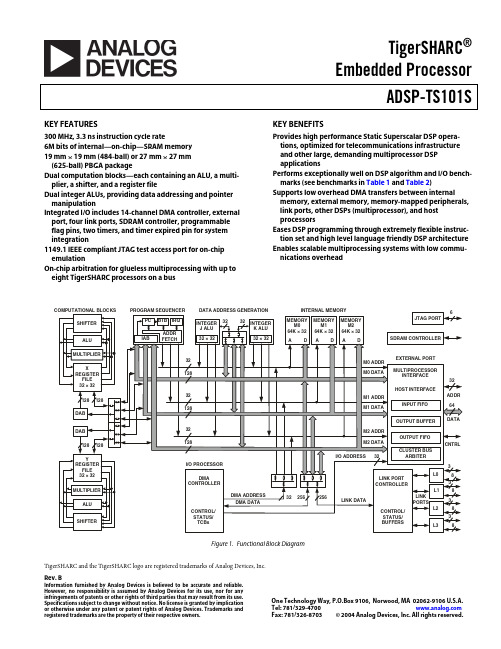
aTigerSHARC and the TigerSHARC logo are registered trademarks of Analog Devices, Inc.TigerSHARC®Embedded ProcessorADSP-TS101SRev. BInformation furnished by Analog Devices is believed to be accurate and reliable. However, no responsibility is assumed by Analog Devices for its use, nor for anyinfringements of patents or other rights of third parties that may result from its use. Specifications subject to change without notice. No license is granted by implication or otherwise under any patent or patent rights of Analog Devices. Trademarks and registered trademarks are the property of their respective owners.One Technology Way, P.O.Box 9106, Norwood, MA 02062-9106 U.S.A. Tel: 781/ Fax: 781/326-8703© 2004 Analog Devices, Inc. All rights reserved.KEY FEATURES300MHz, 3.3ns instruction cycle rate6M bits of internal—on-chip—SRAM memory19 mm×19mm (484-ball) or 27 mm×27mm(625-ball) PBGA packageDual computation blocks—each containing an ALU, a multi-plier, a shifter, and a register fileDual integer ALUs, providing data addressing and pointer manipulationIntegrated I/O includes 14-channel DMA controller, external port, four link ports, SDRAM controller, programmable flag pins, two timers, and timer expired pin for system integration1149.1 IEEE compliant JTAG test access port for on-chip emulationOn-chip arbitration for glueless multiprocessing with up to eight TigerSHARC processors on a bus KEY BENEFITSProvides high performance Static Superscalar DSP opera-tions, optimized for telecommunications infrastructure and other large, demanding multiprocessor DSP applicationsPerforms exceptionally well on DSP algorithm and I/O bench-marks (see benchmarks in Table1 and Table2)Supports low overhead DMA transfers between internal memory, external memory, memory-mapped peripherals, link ports, other DSPs (multiprocessor), and host processorsEases DSP programming through extremely flexible instruc-tion set and high level language friendly DSP architecture Enables scalable multiprocessing systems with low commu-nications overheadFigure 1.Functional Block DiagramADSP-TS101S TABLE OF CONTENTSGeneral Description (3)Dual Compute Blocks (4)Data Alignment Buffer (DAB) (4)Dual Integer ALUs (IALUs) (4)Program Sequencer (5)Interrupt Controller (5)Flexible Instruction Set (5)On-Chip SRAM Memory (5)External Port(Off-Chip Memory/Peripherals Interface) (6)Host Interface (6)Multiprocessor Interface (7)SDRAM Controller (7)EPROM Interface (7)DMA Controller (7)Link Ports (8)Timer and General-Purpose I/O (9)Reset and Booting (9)Low Power Operation (9)Clock Domains (9)Output Pin Drive Strength Control (10)Power Supplies (10)Filtering Reference Voltage and Clocks (10)Development Tools (10)Designing an Emulator-Compatible DSP Board(Target) (11)Additional Information (11)Pin Function Descriptions (12)Pin States at Reset (12)Pin Definitions (12)Strap Pin Function Descriptions (19)Specifications (20)Recommended Operating Conditions (20)Electrical Characteristics (20)Absolute Maximum Ratings (21)ESD Sensitivity (21)Timing Specifications (21)General AC Timing (21)Link Ports Data Transferand Token Switch Timing (29)Output Drive Currents (32)Test Conditions (34)Output Disable Time (34)Output Enable Time (34)Capacitive Loading (34)Environmental Conditions (36)Thermal Characteristics (36)PBGA Pin Configurations (36)Outline Dimensions (43)Ordering Guide (44)REVISION HISTORY12/04—Rev. A to Rev. BProvides more information on clock signals (including a usable jitter specification) in:Reference Clocks—Core Clock (CCLK) Cycle Time (22)Reference Clocks—Local Clock (LCLK) Cycle Time (22)Reference Clocks—System Clock (SCLK) Cycle Time .. 23 Reference Clocks—Test Clock (TCK) Cycle Time (23)Updates input setup times for external port pins in:AC Signal Specifications (for SCLK <16.7 ns) (25)Rev. B|Page 2 of 44|December 2004ADSP-TS101SRev. B |Page 3 of 44|December 2004GENERAL DESCRIPTIONThe ADSP-TS101S TigerSHARC processor is an ultrahigh per-formance, static superscalar processor optimized for large signal processing tasks and communications infrastructure. The DSP combines very wide memory widths with dual computation blocks—supporting 32- and 40-bit floating-point and 8-, 16-, 32-, and 64-bit fixed-point processing—to set a new standard of performance for digital signal processors. The TigerSHARC processor’s static superscalar architecture lets the processor exe-cute up to four instructions each cycle, performing 24 fixed-point (16-bit) operations or six floating-point operations.Three independent 128-bit wide internal data buses, each connecting to one of the three 2M bit memory banks, enable quad word data, instruction, and I/O accesses and provide 14.4G bytes per second of internal memory bandwidth. Operat-ing at 300MHz, the ADSP-TS101S processor’s core has a 3.3ns instruction cycle time. Using its Single-Instruction, Multiple-Data (SIMD) features, the ADSP-TS101S can perform 2.4 bil-lion 40-bit MACs or 600 million 80-bit MACs per second. Table 1 and Table 2 show the DSP’s performance benchmarks.The ADSP-TS101S is code compatible with the otherTigerSHARC processors.The Functional Block Diagram on Page 1 shows the ADSP-TS101S processor’s architectural blocks. These blocks include:•Dual compute blocks, each consisting of an ALU, multi-plier, 64-bit shifter, and 32-word register file and associated data alignment buffers (DABs)•Dual integer ALUs (I ALUs),each with its own 31-word register file for data addressing• A program sequencer with instruction alignment buffer (IAB), branch target buffer (BTB), and interrupt controller •Three 128-bit internal data buses, each connecting to one of three 2M bit memory banks •On-chip SRAM (6M bit)•An external port that provides the interface to host proces-sors, multiprocessing space (DSPs), off-chip memory mapped peripherals, and external SRAM and SDRAM • A 14-channel DMA controller•Four link ports•Two 64-bit interval timers and timer expired pin• A 1149.1 IEEE compliant JTAG test access port for on-chipemulationFigure 2 shows a typical single processor system with external SDRAM. Figure 4 on Page 8 shows a typical multiprocessor system.The TigerSHARC processor uses a Static Superscalar TM † architec-ture. This architecture is superscalar in that the ADSP-TS101S processor’s core can execute simultaneously from one to four 32-bit instructions encoded in a very large instruction word (VLIW) instruction line using the DSP’s dual compute blocks. Because the DSP does not perform instruction reordering at run-time—the programmer selects which operations will exe-cute in parallel prior to run-time—the order of instructions is static.With few exceptions, an instruction line, whether it contains one, two, three, or four 32-bit instructions, executes with a throughput of one cycle in an eight-deep processor pipeline. For optimal DSP program execution, programmers must follow the DSP’s set of instruction parallelism rules when encoding an instruction line. In general, the selection of instructions that the DSP can execute in parallel each cycle depends on the instruc-tion line resources each instruction requires and on the source and destination registers used in the instructions. The program-mer has direct control of three core components—the IALUs, the compute blocks, and the program sequencer.The ADSP-TS101S, in most cases, has a two-cycle arithmetic execution pipeline that is fully interlocked, so whenever a com-putation result is unavailable for another operation dependentTable 1.General-Purpose Algorithm Benchmarks at 300 MHzBenchmark Speed ClockCycles 32-bit algorithm, 600 million MACs/s peak performance 1024 point complex FFT (Radix 2)32.78 µs 9,83550-tap FIR on 1024 input 91.67 µs 27,500Single FIR MAC 1.83 ns 0.5516-bit algorithm, 2.4 billion MACs/s peak performance 256 point complex FFT (Radix 2) 3.67 µs 1,10050-tap FIR on 1024 input 24.0 µs 7,200Single FIR MAC 0.47 ns 0.14Single complex FIR MAC 1.9 ns 0.57I/O DMA transfer rate External port 800M bytes/s n/a Link ports (each)250M bytes/s n/aTable 2.3G Wireless Algorithm BenchmarksBenchmark Execution (MIPS)11The execution speed is in instruction cycles per second.Turbo decode384 kbps data channel 51 MIPS 22This value is for six iterations of the algorithm. For eight iterations of the turbo decoder, this benchmark is 67 MIPS.Viterbi decode12.2 kbps AMR 3 voice channel 3Adaptive multi rate (AMR)0.86 MIPS Complex correlation3.84 Mcps 4 with a spreading factor of 2564Megachips per second (Mcps)0.27 MIPS†Static Superscalar is a trademark of Analog Devices, Inc.ADSP-TS101Son it, the DSP automatically inserts one or more stall cycles as needed. Efficient programming with dependency-free instruc-tions can eliminate most computational and memory transfer data dependencies.In addition, the ADSP-TS101S supports SIMD operations two ways—SIMD compute blocks and SIMD computations.The programmer can direct both compute blocks to operate on the same data (broadcast distribution) or on different data (merged distribution). In addition, each compute block can execute four 16-bit or eight 8-bit SIMD computations in parallel.DUAL COMPUTE BLOCKSThe ADSP-TS101S has compute blocks that can execute com-putations either independently or together as a SIMD engine. The DSP can issue up to two compute instructions per compute block each cycle, instructing the ALU, multiplier, or shifter to perform independent, simultaneous operations.The compute blocks are referred to as X and Y in assembly syn-tax, and each block contains three computational units—an ALU, a multiplier, a 64-bit shifter—and a 32-word register file.•Register file—each compute block has a multiported32-word, fully orthogonal register file used for transferring data between the computation units and data buses and forstoring intermediate results. Instructions can access theregisters in the register file individually (word aligned), or in sets of two (dual aligned) or four (quad aligned).•ALU—the ALU performs a standard set of arithmetic oper-ations in both fixed- and floating-point formats. It alsoperforms logic operations.•Multiplier—the multiplier performs both fixed- and float-ing-point multiplication and fixed-point multiply andaccumulate.•Shifter—the 64-bit shifter performs logical and arithmetic shifts, bit and bit stream manipulation, and field depositand extraction operations.•Accelerator—128-bit unit for trellis decoding (for example, Viterbi and turbo decoders) and complex correlations for communication applications.Using these features, the compute blocks can:•Provide 8 MACs per cycle peak and 7.1 MACs per cyclesustained 16-bit performance and provide 2 MACs percycle peak and 1.8 MACs per cycle sustained 32-bit perfor-mance (based on FIR)•Execute six single precision floating-point or execute 24fixed-point (16-bit) operations per cycle, providing1,800MFLOPS or 7.3GOPS performance•Perform two complex 16-bit MACs per cycle•Execute eight trellis butterflies in one cycleDATA ALIGNMENT BUFFER (DAB)The DAB is a quad word FIFO that enables loading of quad word data from nonaligned addresses. Normally, load instruc-tions must be aligned to their data size so that quad words are loaded from a quad aligned address. Using the DAB signifi-cantly improves the efficiency of some applications, such as FIR filters.DUAL INTEGER ALUS (IALUS)The ADSP-TS101S has two IALUs that provide powerful address generation capabilities and perform many general-pur-pose integer operations. Each of the IALUs:•Provides memory addresses for data and update pointers •Supports circular buffering and bit-reverse addressing •Performs general-purpose integer operations, increasingprogramming flexibility•Includes a 31-word register file for each IALUAs address generators, the IALUs perform immediate or indi-rect (pre- and post-modify) addressing. They perform modulus and bit-reverse operations with no constraints placed on mem-ory addresses for the modulus data buffer placement. Each IALU can specify either a single, dual, or quad word access from memory.The IALUs have hardware support for circular buffers, bit reverse, and zero-overhead looping. Circular buffers facilitate efficient programming of delay lines and other data structures required in digital signal processing, and they are commonlyFigure 2.Single Processor System with External SDRAMRev. B|Page 4 of 44|December 2004ADSP-TS101SRev. B |Page 5 of 44|December 2004used in digital filters and Fourier transforms. Each IALU pro-vides registers for four circular buffers, so applications can set up a total of eight circular buffers. The IALUs handle address pointer wraparound automatically, reducing overhead, increas-ing performance, and simplifying implementation. Circular buffers can start and end at any memory location.Because the IALU’s computational pipeline is one cycle deep, in most cases, integer results are available in the next cycle. Hard-ware (register dependency check) causes a stall if a result is unavailable in a given cycle.PROGRAM SEQUENCERThe ADSP-TS101S processor’s program sequencer supports:• A fully interruptible programming model with flexible pro-gramming in assembly and C/C++ languages; handles hardware interrupts with high throughput and no aborted instruction cycles.•An eight-cycle instruction pipeline—three-cycle fetch pipe and five-cycle execution pipe—with computation results available two cycles after operands are available.•The supply of instruction fetch memory addresses; the sequencer’s instruction alignment buffer (IAB) caches up to five fetched instruction lines waiting to execute; the pro-gram sequencer extracts an instruction line from the IAB and distributes it to the appropriate core component for execution.•The management of program structures and determination of program flow according to JUMP, CALL, RTI, RTS instructions, loop structures, conditions, interrupts, and software exceptions.•Branch prediction and a 128-entry branch target buffer (BTB) to reduce branch delays for efficient execution of conditional and unconditional branch instructions and zero-overhead looping; correctly predicted branches that are taken occur with zero-to-two overhead cycles, over-coming the three-to-six stage branch penalty.•Compact code without the requirement to align code in memory; the IAB handles alignment.Interrupt ControllerThe DSP supports nested and non-nested interrupts. Each interrupt type has a register in the interrupt vector table. Also, each has a bit in both the interrupt latch register and the inter-rupt mask register. All interrupts are fixed as either level sensitive or edge sensitive, except the IRQ3–0 hardware inter-rupts, which are programmable.The DSP distinguishes between hardware interrupts and soft-ware exceptions, handling them differently. When a software exception occurs, the DSP aborts all other instructions in the instruction pipe. When a hardware interrupt occurs, the DSP continues to execute instructions already in the instruction pipe.Flexible Instruction SetThe 128-bit instruction line, which can contain up to four 32-bit instructions, accommodates a variety of parallel operations for concise programming. For example, one instruction line can direct the DSP to conditionally execute a multiply, an add, and a subtract in both computation blocks while it also branches to another location in the program. Some key features of the instruction set include:•Enhanced instructions for communications infrastructure to govern trellis decoding (for example, Viterbi and turbo decoders) and despreading via complex correlations •Algebraic assembly language syntax•Direct support for all DSP, imaging, and video arithmetic types, eliminating hardware modes•Branch prediction encoded in instruction, enables zero-overhead loops•Parallelism encoded in instruction line•Conditional execution optional for all instructions •User-defined, programmable partitioning between pro-gram and data memoryON-CHIP SRAM MEMORYThe ADSP-TS101S has 6M bits of on-chip SRAM memory, divided into three blocks of 2M bits (64K words ×32bits). Each block—M0, M1, and M2—can store program, data, or both, so applications can configure memory to suit specific needs. Plac-ing program instructions and data in different memory blocks, however, enables the DSP to access data while performing an instruction fetch.The DSP’s internal and external memory (Figure 3) is organized into a unified memory map, which defines the location (address) of all elements in the system.The memory map is divided into four memory areas—host space, external memory, multiprocessor space, and internal memory—and each memory space, except host memory, is sub-divided into smaller memory spaces.Each internal memory block connects to one of the 128-bit wide internal buses—block M0 to bus MD0, block M1 to bus MD1, and block M2 to bus MD2—enabling the DSP to perform three memory transfers in the same cycle. The DSP’s internal bus architecture provides a total memory bandwidth of 14.4G bytes per second, enabling the core and I/O to access eight 32-bit data words (256 bits) and four 32-bit instructions each cycle. The DSP’s flexible memory structure enables:•DSP core and I/O access of different memory blocks in the same cycle•DSP core access of all three memory blocks in parallel—one instruction and two data accesses•Programmable partitioning of program and data memory •Program access of all memory as 32-, 64-, or 128-bit words—16-bit words with the DAB•Complete context switch in less than 20 cycles (66ns)ADSP-TS101SEXTERNAL PORT(OFF-CHIP MEMORY/PERIPHERALS INTERFACE)The ADSP-TS101S processor’s external port provides the pro-cessor’s interface to off-chip memory and peripherals. The4G word address space is included in the DSP’s unified address space. The separate on-chip buses—three 128-bit data buses and three 32-bit address buses—are multiplexed at the external port to create an external system bus with a single 64-bit data bus and a single 32-bit address bus. The external port supports data transfer rates of 800M bytes per second over external bus.The external bus can be configured for 32- or 64-bit operation. When the system bus is configured for 64-bit operation, the lower 32 bits of the external data bus connect to even addresses, and the upper 32 bits connect to odd addresses. The external port supports pipelined, slow, and SDRAM proto-cols. Addressing of external memory devices and memory mapped peripherals is facilitated by on-chip decoding of high order address lines to generate memory bank select signals. The ADSP-TS101S provides programmable memory, pipeline depth, and idle cycle for synchronous accesses, and external acknowledge controls to support interfacing to pipelined or slow devices, host processors, and other memory-mapped peripherals with variable access, hold, and disable time requirements.Host InterfaceThe ADSP-TS101S provides an easy and configurable interface between its external bus and host processors through the exter-nal port. To accommodate a variety of host processors, the hostFigure 3.Memory MapRev. B|Page 6 of 44|December 2004ADSP-TS101SRev. B |Page 7 of 44|December 2004interface supports pipelined or slow protocols for accesses of the host as slave. Each protocol has programmable transmission parameters, such as idle cycles, pipe depth, and internal wait cycles.The host interface supports burst transactions initiated by a host processor. After the host issues the starting address of the burst and asserts the BRST signal, the DSP increments the address internally while the host continues to assert BRST.The host interface provides a deadlock recovery mechanism that enables a host to recover from deadlock situations involving the DSP. The BOFF signal provides the deadlock recovery mecha-nism. When the host asserts BOFF, the DSP backs off thecurrent transaction and asserts HBG and relinquishes the exter-nal bus.The host can directly read or write the internal memory of the ADSP-TS101S, and it can access most of the DSP registers, including DMA control (TCB) registers. Vector interrupts sup-port efficient execution of host commands.Multiprocessor InterfaceThe ADSP-TS101S offers powerful features tailored to multi-processing DSP systems through the external port and link ports. This multiprocessing capability provides highest band-width for interprocessor communication, including:•Up to eight DSPs on a common bus•On-chip arbitration for glueless multiprocessing •Link ports for point-to-point communicationThe external port and link ports provide integrated, glueless multiprocessing support.The external port supports a unified address space (see Figure 3) that enables direct interprocessor accesses of each ADSP-TS101S processor’s internal memory and registers. The DSP’s on-chip distributed bus arbitration logic provides simple, glue-less connection for systems containing up to eight ADSP-TS101S processors and a host processor. Bus arbitration has a rotating priority. Bus lock supports indivisible read-modify-write sequences for semaphores. A bus fairness feature prevents one DSP from holding the external bus too long.The DSP’s four link ports provide a second path for interproces-sor communications with throughput of 1G bytes per second. The cluster bus provides 800M bytes per second throughput—with a total of 1.8G bytes per second interprocessor bandwidth.SDRAM ControllerThe SDRAM controller controls the ADSP-TS101S processor’s transfers of data to and from synchronous DRAM (SDRAM). The throughput is 32 or 64 bits per SCLK cycle using the exter-nal port and SDRAM control pins.The SDRAM interface provides a glueless interface with stan-dard SDRAMs—16M bit, 64M bit, 128M bit, and 256M bit. The DSP directly supports a maximum of 64M words ×32bits of SDRAM. The SDRAM interface is mapped in external memory in the DSP’s unified memory map.EPROM InterfaceThe ADSP-TS101S can be configured to boot from external 8-bit EPROM at reset through the external port. An automatic process (which follows reset) loads a program from the EPROM into internal memory. This process uses 16 wait cycles for each read access. During booting, the BMS pin functions as theEPROM chip select signal. The EPROM boot procedure uses DMA Channel 0, which packs the bytes into 32-bit instructions. Applications can also access the EPROM (write flash memories) during normal operation through DMA.The EPROM or flash memory interface is not mapped in the DSP’s unified memory map. It is a byte address space limited to a maximum of 16M bytes (24 address bits). The EPROM or flash memory interface can be used after boot via a DMA.DMA CONTROLLERThe ADSP-TS101S processor’s on-chip DMA controller, with 14 DMA channels, provides zero-overhead data transfers with-out processor intervention. The DMA controller operates independently and invisibly to the DSP’s core, enabling DMA operations to occur while the DSP’s core continues to execute program instructions. The DMA controller performs DMA transfers between:•Internal memory and external memory and memory-mapped peripherals•Internal memory of other DSPs on a common bus, a host processor, or link port I/O•External memory and external peripherals or link port I/O •External bus master and internal memory or link port I/O The DMA controller provides a number of additional features.The DMA controller supports flyby transfers. Flyby operations only occur through the external port (DMA Channel 0) and do not involve the DSP’s core. The DMA controller acts as a con-duit to transfer data from one external device to another through external memory. During a transaction, the DSP:•Relinquishes the external data bus•Outputs addresses, memory selects (MS1–0, MSSD, RAS, CAS, and SDWE) and the FLYBY, IOEN, and RD/WR strobes•Responds toACKDMA chaining is also supported by the DMA controller. DMA chaining operations enable applications to automatically link one DMA transfer sequence to another for continuous trans-mission. The sequences can occur over different DMA channels and have different transmission attributes.The DMA controller also supports two-dimensional transfers. The DMA controller can access and transfer two-dimensional memory arrays on any DMA transmit or receive channel. These transfers are implemented with index, count, and modify regis-ters for both the X and Y dimensions.ADSP-TS101SThe DMA controller performs the following DMA operations:•External port block transfers. Four dedicated bidirectional DMA channels transfer blocks of data between the DSP’s internal memory and any external memory or memory-mapped peripheral on the external bus. These transferssupport master mode and handshake mode protocols.•Link port transfers. Eight dedicated DMA channels (four transmit and four receive) transfer quad word data onlybetween link ports and between a link port and internal orexternal memory. These transfers only use handshakemode protocol. DMA priority rotates between the fourreceive channels.•AutoDMA transfers. Two dedicated unidirectional DMA channels transfer data received from an external bus master to internal memory or to link port I/O. These transfers only use slave mode protocol, and an external bus master must initiate the transfer.LINK PORTSThe DSP’s four link ports provide additional 8-bit bidirectional I/O capability. With the ability to operate at a double data rate—latching data on both the rising and falling edges of the clock—Figure 4.Shared Memory Multiprocessing SystemRev. B|Page 8 of 44|December 2004ADSP-TS101SRev. B |Page 9 of 44|December 2004running at 125MHz, each link port can support up to250M bytes per second, for a combined maximum throughput of 1G bytes per second.The link ports provide an optional communications channel that is useful in multiprocessor systems for implementing point to point interprocessor communications. Applications can also use the link ports for booting.Each link port has its own double-buffered input and output registers. The DSP’s core can write directly to a link port’s trans-mit register and read from a receive register, or the DMA controller can perform DMA transfers through eight (four transmit and four receive) dedicated link port DMA channels. Each link port has three signals that control its operation. LxCLKOUT and LxCLKIN implement clock/acknowledge handshaking. LxDIR indicates the direction of transfer and is used only when buffering the LxDAT signals. An example appli-cation would be using differential low-swing buffers for long twisted-pair wires. LxDAT provides the 8-bit data bus input/output.Applications can program separate error detection mechanisms for transmit and receive operations (applications can use the checksum mechanism to implement consecutive link porttransfers), the size of data packets, and the speed at which bytes are transmitted.Under certain conditions, the link port receiver can initiate a token switch to reverse the direction of transfer; the transmitter becomes the receiver and vice versa.TIMER AND GENERAL-PURPOSE I/OThe ADSP-TS101S has a timer pin (TMR0E) that generates out-put when a programmed timer counter has expired. Also, the DSP has four programmable general-purpose I/O pins(FLAG3–0) that can function as either single bit input or out-put. As outputs, these pins can signal peripheral devices; as inputs, they can provide the test for conditional branching.RESET AND BOOTINGThe ADSP-TS101S has two levels of reset (see reset specifica-tions on Page 24):•Power-up reset—after power-up of the system, and strap options are stable, the RESET pin must be asserted (low). •Normal reset—for any resets following the power-up reset sequence, the RESET pin must be asserted.The DSP can be reset internally (core reset) by setting the SWRST bit in SQCTL. The core is reset, but not the external port or I/O.After reset, the ADSP-TS101S has four boot options for begin-ning operation:•Boot from EPROM. The DSP defaults to EPROM booting when the BMS pin strap option is set low. See Strap Pin Function Descriptions on Page 19.•Boot by an external master (host or another ADSP-TS101S). Any master on the cluster bus can boot the ADSP-TS101S through writes to its internal memory or through autoDMA.•Boot by link port. All four receive link DMA channels are initialized after reset to transfer a 256-word block to inter-nal memory address 0 to 255, and to issue an interrupt at the end of the block (similar to EP DMA). The correspond-ing DMA interrupts are set to address zero (0).•No boot—Start running from an external memory. Using the “no boot” option, the ADSP-TS101S must start running from an external memory, caused by asserting one of the IRQ3–0 interrupt signals.The ADSP-TS101S core always exits from reset in the idle state and waits for an interrupt. Some of the interrupts in the inter-rupt vector table are initialized and enabled after reset.LOW POWER OPERATIONThe ADSP-TS101S can enter a low power sleep mode in which its core does not execute instructions, reducing power con-sumption to a minimum. The ADSP-TS101S exits sleep mode when it senses a falling edge on any of its IRQ3–0 interrupt inputs. The interrupt, if enabled, causes the ADSP-TS101S to execute the corresponding interrupt service routine. This fea-ture is useful for systems that require a low power standby mode.CLOCK DOMAINSAs shown in Figure 5, the ADSP-TS101S has two clock inputs, SCLK (system clock) and LCLK (local clock).These inputs drive its two major clock domains:•SCLK (system clock). Provides clock input for the external bus interface and defines the ac specification reference for the external bus signals. The external bus interface runs at 1× the SCLK frequency. A DLL locks internal SCLK to SCLK input.•LCLK (local clock). Provides clock input to the internal clock driver, CCLK, which is the internal clock for the core, internal buses, memory, and link ports. The instructionFigure 5.Clock Domains。
自动排渣过滤器SBY、SBL
过滤器>>自动排渣过滤器>>自动排渣过滤器产品详细信息过滤器系列价格供用户或设计院工程项目做预算一、阀门的选型步骤1.明确阀门在设备或装置中的用途,确定阀门的工作条件:适用介质、工作压力、工作温度等等。
2.确定与阀门连接管道的公称通径和连接方式:法兰、螺纹、焊接等。
3.确定操作阀门的方式:手动、电动、电磁、气动或液动、电气联动或电液联动等。
4.根据管线输送的介质、工作压力、工作温度确定所选阀门的壳体和内件的材料:灰铸铁、可锻铸铁、球墨铸铁、碳素钢、合金钢、不锈耐酸钢、铜合金等。
5.确定阀门的型式:闸阀、截止阀、球阀、蝶阀、节流阀、安全阀、减压阀、蒸汽疏水阀、等。
6.确定阀门的参数:对于自动阀门,根据不同需要先确定允许流阻、排放能力、背压等,再确定管道的公称通径和阀座孔的直径。
7.确定所选用阀门的几何参数:结构长度、法兰连接形式及尺寸、开启和关闭后阀门高度方向的尺寸、连接的螺栓孔尺寸和数量、整个阀门外型尺寸等。
8.利用现有的资料:阀门产品目录、阀门产品样本等选型适当的阀门产品。
二、阀门的选型依据1.所选用阀门的用途、使用工况条件和操纵控制方式。
2.工作介质的性质:工作压力、工作温度、腐蚀性能,是否含有固体颗粒,介质是否有毒,是否是易燃、易爆介质,介质的黏度等等。
3.对阀门流体特性的要求:流阻、排放能力、流量特性、密封等级等等。
4.安装尺寸和外形尺寸要求:公称通径、与管道的连接方式和连接尺寸、外形尺寸或重量限制等。
⑤对阀门产品的可靠性、使用寿命和电动装置的防爆性能等的附加要求。
(在选定参数时应注意:如果阀门要用于控制目的,必须确定如下额外参数:操作方法、最大和最小流量要求、正常流动的压力降、关闭时的压力降、阀门的最大和最小进口压力。
)根据上述选型阀门的依据和步骤,合理、正确地选型阀门时还必须对各种类型阀门的内部结构进行详细了解,以便能对优先选用的阀门做出正确的抉择。
管道的最终控制是阀门。
isis中英文元件名称对照解读
AD芯片-----TECHWELL TW6805A仿真软件里的AD0809有问题,用0808代替定时/计数器的使用方法:CLK:计数和测频状态时,数字波的输入端。
(counter enable)CE:计数使能端;通过属性设置高还是低有效。
无效暂停计数RST:复位端(RESET),可设上升沿(Low-High)或者下降沿(High-Low)有效。
4种工作方式:通过属性Operating Mode 来选择。
Default : 缺省方式,计数器方式。
Time(secs):100S定时方式,由CE和RST 控制暂停和重新开始。
Time(hms):10小时定时方式,同上。
Frequency: 测频方式,CE和RST有效时,显示CLK端数字波频率Count:计数方式。
+++++++++++++++++++++++++++++++++ ++++++++++++++++++++++++++++常用元件列表:POT-HG 可调电位器7SEG-MPX8-CC-BLUE 8位数码管COMPIM 串口SW- 开关7SEG-BCD 含译码驱动的数显Speaker 扬声器2N5771和2N5772,15V对管300MARES , CAP,BUTTON 按钮开关KEYPAD-PHONE 3*4电话键盘KEYPAD-SMALLCALC 4*4计算器键盘KEYPAD-CALCULATOR 4*6计算器键盘PG160128A 128*128液晶++++++++元件库详细分类1.analog ics 模拟集成器件8个子类:amplifier 放大器comparators 比较器display drivers 显示驱动器filters 滤波器miscellaneous 混杂器件regulators 三端稳压器timers 555定时器voltage references 参考电压2,capacitors CAP电容,23个分类别animated 可显示充放电电荷电容audio grade axial 音响专用电容axial lead polypropene 径向轴引线聚丙烯电容axial lead polystyrene 径向轴引线聚苯乙烯电容ceramic disc 陶瓷圆片电容decoupling disc 解耦圆片电容high temp radial 高温径向电容high temp axial electrolytic高温径向电解电容metallised polyester film 金属聚酯膜电容metallised polypropene 金属聚丙烯电容metallised polypropene film 金属聚丙烯膜电容miniture electrolytic 微型电解电容multilayer metallised polyester film 多层金属聚酯膜电容mylar film 聚酯薄膜电容nickel barrier 镍栅电容non polarised 无极性电容polyester layer 聚酯层电容radial electrolytic 径向电解电容resin dipped 树脂蚀刻电容tantalum bead 钽珠电容variable 可变电容vx a xial electrolytic VX 轴电解电容3,CMOS 4000 series 4000系列数字电路adders 加法器buffers & drivers 缓冲和驱动器comparators 比较器counters 计数器decoders 译码器encoders 编码器flip-flops & latches 触发器和锁存器frequency dividers & tiner 分频和定时器gates & inverters 门电路和反相器memory 存储器misc.logic 混杂逻辑电路mutiplexers 数据选择器multivibrators 多谐振荡器phase-locked loops(PLL) 锁相环registers 寄存器signal switcher 信号开关4,connectors 接头;8个分类:audio 音频接头D-type D型接头DIL 双排插座header blocks 插头miscellaneous 各种接头PCB transfer PCB 传输接头SIL 单盘插座ribbon cable 蛇皮电缆terminal blocks 接线端子台5,data converters 数据转换器:4个分类:A/D converters 模数转换器D/A converters 数模转换器sample & hold 采样保持器temperature sensors 温度传感器6,debugging tools 调试工具数据:3个类别:breakpoint triggers 断点触发器logic probes 逻辑输出探针logic timuli 逻辑状态输入7,diodes 二极管;8个分类:bridge rectifiers 整流桥generic 普通二极管rectifiers 整流二极管schottky 肖特基二极管switching 开关二极管tunnel 隧道二极管varicap 稳压二极管8,inductors 电感:3个类别:generic 普通电感SMT inductors 表面安装技术电感transformers 变压器9,laplace primitives 拉普拉斯模型:7个类别:1st order 一阶模型2nd order 二阶模型controllers 控制器non-linear 非线性模型operators 算子poles/zeros 极点/零点symbols 符号10,memory ICs 存储器芯片:7个分类:dynamic RAM 动态数据存储器EEPROM 电可擦出程序存储器EPROM 可擦出程序存储器I2C memories I2C 总线存储器memory cards 存储卡SPI Memories SPI 总线存储器static RAM 静态数据存储器11,microprocessor ICs 微处理器:13个分类:12,modelling primitivvves 建模源:9个分类:13,operational amplifiers 运算放大器:7个分类:dual 双运放ideal 理想运放macromodel 大量使用的运放octal 8运放quad 4运放single 单运放triple 三运放14,optoelectronics 光电器件:11个分类:7-segment displays 7段显示alphanumeric LCDs 液晶数码显示bargraph displays 条形显示dot matrix displays 点阵显示graphical LCDs 液晶图形显示lamps 灯LCD controllers 液晶控制器LCD controllers 液晶面板显示LEDs 发光二极管optocouplers 光电耦合serial LCDs 串行液晶显示15,resistors 电阻:11个分类:0.6w metal film 0.6w金属膜电阻10 watt wirewound 10w绕线电阻2w metal film 2w 金属膜电阻3 watt wirewound 3w 绕线电阻7 watt wirewound 7w 绕线电阻generix 普通电阻high voltage 高压电阻NTC 负温度系数热敏电阻resistor packs 排阻variable 滑动变阻器varisitors可变电阻参考试验中采用的可变电阻是:POT-HG16,simulator primitives 仿真源:3个类别:flip-flops 触发器gates 门电路sources 电源17,switches and relays 开关和继电器:4个类别:key pads 键盘relays 普通继电器relays(specific) 专用继电器switches 开关18,switching devices 开关器件:4个分类:DIACs 两端交流开关generic 普通开关元件SCRs 可控硅TRIACs 三端双向可控硅19,真空管:20,传感器:2个分类:pressure 压力传感器temperature 温度传感器21,晶体管:8个分类:bipolar 双极型晶体管generic 普通晶体管(错误)IGBT 绝缘栅双极晶体管JFET 结型场效应管MOSFET 金属氧化物场效应管RF power LDMOS 射频功率LDMOS管RF power VDMOS 射频功率VDMOS管unijunction 单结晶体管Electromechanical 电机MOTOR AC 交流电机MOTOR SERVO 伺服电机双相步进电机motor-bistepper(Bipolar Stepper Motor),四相步进电机motor-stepper(unipolar stepper motor)驱动电路,用ULN2003可以,proteus中推荐的L298和L6201(电子元件-步进电机中有L298资料)+++++++++++++++++++++++++++++++++ +++++++++++++++++++++++++++++++++ +++步进电机,可以用MTD2003,UN2916等专用芯片Proteus中图形液晶模块驱动芯片一览表LM3228 LM3229 LM3267 LM3283LM3287 LM4228 LM4265 LM4267LM4283 LM4287 PG12864F PG24064FPG128128A PG160128AAGM1232G EW12A03GL Y HDM32GS12-B HDM32GS12Y-B HDG12864F-1 HDS12864F-3 HDG12864L-4 HDG12864L-6NOKIA7110 TG126410GFSB TG13650FEYAMPIRE128x64 LGM12641BS1R PROTEUS原理图元器件库详细说明Device.lib 单双向可控硅、包括电阻、电容、二极管、三极管和PCB的连接器符号、ACTIVE.LIB 包括虚拟仪器和有源器件、拨动开关、键盘、可调电位器和开关、DIODE.LIB 包括二极管和整流桥、稳压管、变容二极管、大功率二极管、高速二极管、可控硅、DISPLAY.LIB 包括LCD、LED、LED 阵列BIPOLAR.LIB 包括三极管FET.LIB 包括场效应管ASIMMDLS.LIB 包括模拟元器件AS 稳压二极管、全桥、74系列、及其他。