电源芯片 《UC3846电流型PWM控制芯片》.
电流型PWM控制芯片UC3844的基本原理

电流型PWM控制芯片UC3844的基本原理
UC3844是美国Unitrode公司(已被TI公司收购)生产的高性能电流型脉宽调制器(PWM)控制器。
早期的PWM控制器是电压控制型的,常用的电压型PWM控制器有TL494、TL495、SG3524、SG3525等。
电压型PWM是指控制器按反馈电压来调节输出脉宽,电流型PWM是指控制器按反馈电流来调节输出脉宽。
电流型PWM是在脉宽比较器的输入端,直接用流过输出电感线圈电流的信号与误差放大器输出信号进行比较,从而调节占空比,使输出的电感峰值电流跟随误差电压变化而变化。
由于结构上有电压环、电流环双环系统,因此,无论开关电源的电压调整率、负载调整率和瞬态响应特性都有提高,是目前比较理想的新型PWM控制器。
电流型PWM
电流型PWM正是针对电压PWM型的缺点发展起来的。
它在原有的电压环上增加了电流反馈环节,构成电压电流双闭环控制。
内环为电流控制环,外环为电压控制环。
无论电流的变化,还是电压的变化,都会使PWM 输出脉冲占空比发生变化。
这种控制方式可改善系统的电压调整率,提高系统的瞬态响应速度,增加系统的稳定性。
其控制系统框图如图2所示。
uc3846中文资料
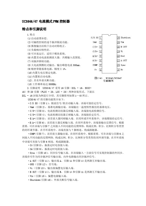
UC3846/47电流模式PWM控制器特点和引脚说明1.特点(1)自动前馈补偿。
(2)可编程控制的逐个脉冲限流功能。
(3)推挽输出结构下自动对称校正。
(4)负载响应特性好。
(5)可并连运行,适用于模块系统。
(6)内置差动电流检测放大器,共模输入范围宽。
(7)双脉冲抑制功能。
(8)大电流图腾柱式输出,输出峰值电流500mA。
(9)精密带隙基准电源,精度士1%。
(10)内置欠电压锁定电路。
(11)内置软启动电路。
(12).具有外部关断功能。
(13)工作频率高达500KHz2.引脚说明 UC3846/47采用16引脚(DIL - 16、SOIC-16)和20引脚(PLCC - 20、LCC - 20)两种封装形式。
下面以DIL - 16封装为例进行介绍,其引脚排列如图1—40所示。
UC3846/47的引脚功能简介如下:·C/S SS(引脚1):限流信号/软启动输入端。
该端可接给定信号。
·V REF (引脚2):基准电源输出端。
该端输出一温度特性极佳的基准电压。
·C/S-(引脚3):电流检测比较器反相输入端。
该端接电流检测信号。
·C/S+(引脚4):电流检测比较器正相输入端。
该端接给定信号。
·E/A+(引脚5):误差放大器同相输入端。
在闭环或开环系统中,该端都接给定信号。
·E/A-(引脚6):误差放大器反相输入端。
在闭环系统中,该端接输出反馈信号。
根据需要,可在该端与引脚7之间接入不同功能的反馈网络,构成比例,积分,比例积分等类型的闭环调节器。
在开环系统中,该端直接与7脚相连,构成跟随器。
·COMP(引脚7):误差放大器输出端。
在闭环系统中,根据需要,可在该端与引脚6之间接入不同功能的反馈网络,构成比例,积分,比例积分等类型的闭环调节器。
在开环系统中该端可直接与引脚6相连,构成跟随器。
·C T(引脚8):振荡定时电容接入端。
稳压电源PWM调制芯片UC3846的应用
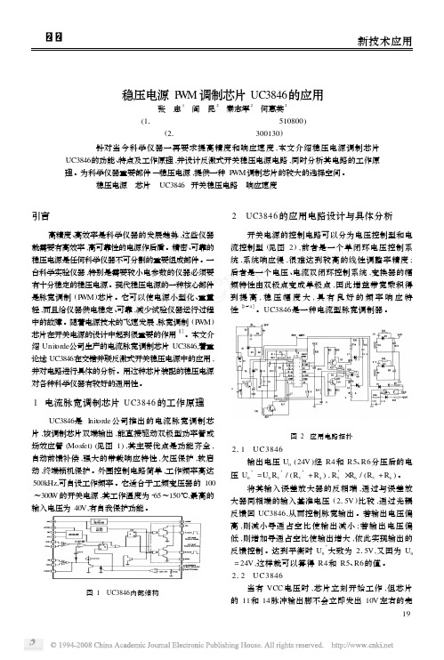
1 电流脉宽调制芯片 UC3846 的工作原理
UC3846是 Initorde公司推出的电流脉宽调制芯 片 ,该调制芯片双端输出 ,能直接驱动双极型功率管或 场效应管 (Mosfet) (见图 1) ,其主要优点是功能齐全 , 自动前馈补偿 ,强大的带载响应特性 ,欠压保护 ,软启 动 ,终端锁机保护。外围控制电路简单 ,工作频率高达 500kHz,可自设工作频率。它适合于工频变压器的 100 ~300W 的开关电源 ,其工作温度为 265~150℃,最高的 输入电压为 40V,有自我保护功能。
(21Hebei University of Technology, Tianjin 300130)
Abstract To abvance the accuracy and response speed of scientific instruments nowdays, the function, characteris2 tics, and operation p rincip le of UC3846 are introduced in this paper. Designs a flyback sw itch voltage - stabilized source circuit using the UC3846, analyses the working p rincip les of this ciruit. It is one of PWM chip s for compo2 nents of scientific instruments. Key words UC3846 Flyback sw itch voltage - stabilized circuit Accuracy Response speed
峰值电流模式控制总结(完整版)
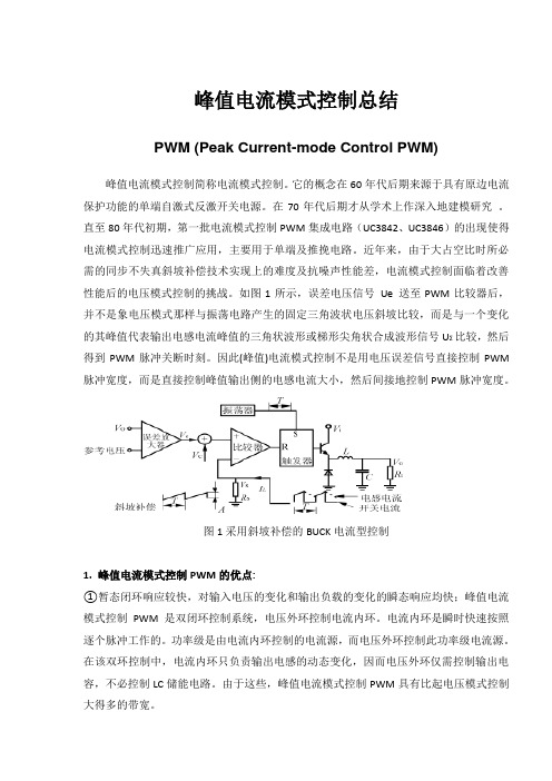
峰值电流模式控制总结PWM (Peak Current-mode Control PWM)峰值电流模式控制简称电流模式控制。
它的概念在60年代后期来源于具有原边电流保护功能的单端自激式反激开关电源。
在70年代后期才从学术上作深入地建模研究。
直至80年代初期,第一批电流模式控制PWM集成电路(UC3842、UC3846)的出现使得电流模式控制迅速推广应用,主要用于单端及推挽电路。
近年来,由于大占空比时所必需的同步不失真斜坡补偿技术实现上的难度及抗噪声性能差,电流模式控制面临着改善性能后的电压模式控制的挑战。
如图1所示,误差电压信号Ue 送至PWM比较器后,并不是象电压模式那样与振荡电路产生的固定三角波状电压斜坡比较,而是与一个变化的其峰值代表输出电感电流峰值的三角状波形或梯形尖角状合成波形信号UΣ比较,然后得到PWM脉冲关断时刻。
因此(峰值)电流模式控制不是用电压误差信号直接控制PWM 脉冲宽度,而是直接控制峰值输出侧的电感电流大小,然后间接地控制PWM脉冲宽度。
图1采用斜坡补偿的BUCK电流型控制1. 峰值电流模式控制PWM的优点:①暂态闭环响应较快,对输入电压的变化和输出负载的变化的瞬态响应均快;峰值电流模式控制PWM是双闭环控制系统,电压外环控制电流内环。
电流内环是瞬时快速按照逐个脉冲工作的。
功率级是由电流内环控制的电流源,而电压外环控制此功率级电流源。
在该双环控制中,电流内环只负责输出电感的动态变化,因而电压外环仅需控制输出电容,不必控制LC储能电路。
由于这些,峰值电流模式控制PWM具有比起电压模式控制大得多的带宽。
②虽然电源的L-C滤波电路为二阶电路,但增加了电流内环控制后,只有当误差电压发生变化时,才会导致电感电流发生变化。
即误差电压决定电感电流上升的程度,进而决定功率开关的占空比。
因此,可看作是一个电流源,电感电流与负载电流之间有了一定的约束关系,使电感电流不再是独立变量,整个反馈电路变成了一阶电路,由于反馈信号电路与电压型相比,减少了一阶,因此误差放大器的控制环补偿网络得以简化,稳定度得以提高并且改善了频响,具有更大的增益带宽乘积。
采用电流控制型PWM芯片UC3843设计反激式电源
电子科技0 引言定频调宽的PWM闭环反馈控制系统,主要有两种反馈控制模式:电流控制型和电压控制型。
由于电流控制型PWM具有以下优点:①暂态闭环响应较快;②控制环易于设计;③输入电压的调整可与电压模式控制的输入电压前馈技术相妣美;④简单自动的磁通平衡功能;⑤瞬时峰值电流限流功能。
又由于反激式变换器具有电路简单、输入和输出之间电气隔离、电压上升和下降范围大等优点,故采用电流控制型PWM及反激式拓扑设计本反激式电源。
本文简要论述电流控制型反激式变换器的工作原理,介绍了UC3843电流控制型脉宽调制器如何使用,并给出了设计方法的实例与测试结果。
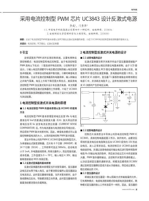
1 电流控制型反激式开关电源的原理■1.1 电流控制型PWM的基本原理以及UC3843 的使用方法电流控制型PWM基本原理是将电压反馈Vfb 与电压基准信号Vref的差通过误差放大器(E/A)放大得出的误差电压信号 Ve 送至电流反馈比较器(CURRENT SENSE COMPARATOR)后,作为电流基准与电流检测信号相比较,然后得到PWM脉冲关断时刻。
因此,峰值电流模式可以直接控制峰值电流的大小,从而间接地控制PWM脉冲宽度。
意法半导体公司的PWM IC UC3843是电流控制型芯片,为单端输出式脉宽调制器。
芯片有 8个引脚(MINIDIP)和14个引脚(SO14),工作频率可高达500kHz,启动电流小于1mA,外电路接线简单,所用元器件少,而且性能优越,成本低廉,工作温度为0~70℃,输入电压≤30V,输出能够直接驱动MOS场效应管。
■1.2 反激式变换器的基本原理反激式变换器的基本原理是当开关管导通时,变压器原边电压近似等于输入电压,由于整流管反偏所以变压器副边无电流流过,此时变压器储存能量。
当开关管关断时,由于各线圈电压反向,导致整流管正向导通,此时变压器储存的能量流经整流管向负载释放。
2 电流控制型反激式开关电源的设计■2.1 功率电路的设计反激式变换器功率开关断开时由于变压器漏感储能产生的电压尖峰须加以相应的箝位电路来抑制。
uc3844开关电源工作原理

uc3844开关电源工作原理UC3844是一种常见的开关电源控制芯片,其工作原理是通过PWM(脉宽调制)控制开关管的通断时间,从而实现电源输出电压的稳定和可控。
UC3844芯片主要由比较器、PWM控制器、参考电压源、误差放大器、内部振荡器及输出级等功能模块组成。
下面我们详细介绍UC3844开关电源的工作原理:1. 参考电压源和误差放大器UC3844芯片内置的参考电压源和误差放大器,用于将输出电压与设定值进行比较,并将比较结果作为控制信号反馈到PWM控制器中。
具体来说,参考电压源会将设定值转化为一个固定的电压信号,而误差放大器则会将输出电压转化为电压信号并与参考电压进行比较。
如果输出电压小于设定值,则误差放大器会输出一个较大的电压信号,反之若输出电压大于设定值,则误差放大器会输出一个较小的电压信号。
这个信号最终被送入PWM控制器,用于调节开关管的通断时间。
2. PWM控制器PWM控制器是UC3844芯片中最为核心的模块之一,其主要作用是控制开关管的通断时间以实现输出电压的稳定控制。
由于PWM控制器内置内部振荡器,因此其可以产生一个固定的周期和占空比。
当误差放大器输出一个控制信号时,PWM控制器会通过比较器将其与内部振荡器的信号进行比较,并在下一个周期开始时调整开关管的通断时间。
如果误差放大器输出的信号大于内部振荡器信号,则PWM控制器会延长开关管的通断时间,反之则会缩短开关管的通断时间。
通过这样不断调节开关管的通断时间,PWM控制器最终可以实现对输出电压的精确控制。
3. 输出级输出级是UC3844芯片中用于输出电源的部分,其主要由开关管、电感和输出电容组成。
开关管的通断状态由PWM控制器控制,当开关管导通时电流会经过电感储存能量,在开关管断开时则会释放出来,从而驱动输出电路中的输出电容产生稳定的输出电压。
输出级中还会加入过载保护电路,用于保护电源系统免受过载和短路等情况的影响。
UC3844开关电源的工作原理是通过反馈控制和PWM调制技术实现对输出电压的精确控制,从而保证电源系统的稳定性和可靠性。
基于UC3846的有源嵌位单级PFC开关电源
基于UC3846的有源嵌位单级PFC开关电源文立群;肖强晖【摘要】设计了一种基于PWM控制芯片UC3846的恒压源,其适用于175~265 V宽电压的交流输入,额定输出电压为24 V,输出电流为2 A。
采用单级三端PFC校正技术,提高系统的功率因数;采用有源嵌位软开关技术,降低开关应力,提高电源的输出效率。
仿真和实物测试结果表明,本恒压源的输入功率因数可达到0.992;在额定负载下,整机效率可达到88%以上。
%A constant voltage source based on PWM control chip UC3846 is designed, which applies to the 175~265 V AC input voltage, and the rated output voltage is 24 V and output current is 2 A. The single stage PFC-three terminal correction technique is used to enhance the power factor of the system;meanwhile,the active clamping-soft switch technology is used to reduce the switch stress and improve the output efficiency of the power. The simulation and physical test shows that the input power factor of the constant voltage source is 0.992 and the system efficiency reaches88%under the rated load.【期刊名称】《湖南工业大学学报》【年(卷),期】2014(000)002【总页数】4页(P52-55)【关键词】UC3846;单级PFC;有源嵌位;软开关【作者】文立群;肖强晖【作者单位】湖南工业大学电气与信息工程学院,湖南株洲 412007;湖南工业大学电气与信息工程学院,湖南株洲 412007【正文语种】中文【中图分类】TP17对电力电子装置而言,高功率因数能够有效减少其对电网的谐波污染。
uc3846中文资料 (2)
UC3846中文资料摘要UC3846是一款高性能的PWM控制器芯片,常用于开关电源的设计。
本文档将介绍UC3846的特点、工作原理、引脚功能、Typical Application和常见问题解答等内容,为读者提供详细的中文资料。
1. 引言UC3846是由德州仪器公司推出的一款PWM控制器,采用复合型器件集成电路的设计。
它具有高性能、稳定可靠和简单易用等优点,广泛应用于电力电子领域中开关电源的设计。
2. 特点UC3846具有以下特点: - 采用复合型器件集成电路设计,集成度高。
- 双弹设计,实现双层反馈控制。
- 宽工作电压范围。
- 内置软起动功能,提高系统可靠性。
- 内置过电流保护、过热保护等多种保护功能。
3. 工作原理UC3846是一款全桥控制器,用于控制开关电源的开关管工作,默认工作周期为50kHz。
其工作原理如下:1.外部反馈信号进入UC3846芯片,经过比较、滤波和放大后得到控制信号。
2.控制信号经过逻辑电路处理,驱动UC3846内部的PWM生成器。
3.PWM生成器根据控制信号产生一个50kHz的方波,用于驱动开关管。
4.开关管的开关动作控制了输出电压的稳定性。
4. 引脚功能UC3846的引脚功能如下: - VCC: 芯片供电引脚。
- GND:地引脚。
- RT/CT: 外部电阻电容网络的引脚。
- COMP: 外部反馈信号输入引脚。
- UVLO: 低电压锁定引脚。
- INV: 输入电压检测引脚。
- FB: 反馈引脚。
- SYNC: 同步引脚。
5. Typical ApplicationUC3846的典型应用包括开关电源、电池充电器、直流变换器等。
下图是一个基于UC3846的开关电源Typical Application示意图。
UC3846 Typical Application6. 常见问题解答6.1 如何选择外部电阻和电容?在选择外部电阻和电容时,需要根据具体应用的设计要求来确定。
电流控制型pwm控制芯片

摘要:介绍并比较了电压控制型和电流控制型DC/DC变换器的基本原理,设计出了基于电流控制型PWM 控制芯片UC3846的大功率DC/DC变换器的实用电路,提出了两种UC3846输出脉冲封锁方式,设计出一种新颖的IGBT驱动电路,实验结果证明,该电路具有较好的控制特性和稳定性。
关键词:DC/DC变换器;脉宽调制;电压控制型;电流控制型;IGBT驱动0 引言随着工业、航空、航天、军事等应用领域技术的不断发展,人们对开关稳压电源的要求也越来越高。
某系统对大功率开关稳压电源提出的要求是:输入电压为AC220V,输出电压为DC38V,输出电流为100A。
开关电源的结构一般为先进行AC/DC然后再DC/DC的形式,考虑到论文篇幅的限制,仅对DC/DC变换部分进行讨论。
大功率DC/DC变换器主电路拓扑有很多种,诸如双管正激式、推挽式、半桥式和全桥式等。
控制芯片的种类也非常多,主要分为电流控制型与电压控制型两大类。
电压控制型只对输出电压采样,作为反馈信号进行闭环控制,采用PWM技术调节输出电压,从控制理论的角度看,这是一种单环控制系统。
电流控制型是在电压控制型的基础上,增加一个电流负反馈环节,使其成为双环控制系统,从而提高了电源的性能。
根据对各种拓扑和控制方式的技术成熟程度,工程化实现难度,电气性能以及成本等指标的比较,本文选用半桥式DC/DC变换器作为主电路,电流型PWM控制芯片UC3846作为该系统的控制单元。
1 电压控制型脉宽调制器和电流控制型脉宽调制器图1为电压控制型变换器的原理框图。
电源输出电压的采样反馈值V f与参考电压V r进行比较放大,得到误差信号V e,它与锯齿波信号比较后,PWM比较器输出PWM控制信号,经驱动电路驱动开关管通断,产生高频方波电压,由高频变压器传输至副方,经整流滤波得到所需要的电压。
改变电压给定V r,即可改变输出电压V o。
图1 电压控制型的原理图图2为电流控制型变换器的原理框图。
UC3846脉宽调制高频开关稳压
课程设计说明书题目 UC3846脉宽调制高频开关稳压(院)系电气与信息工程系专业自动化班级学号学生姓名指导老师姓名完成日期 2008 年 6 月 10 日至2008 年 6 月 20 日湖南工程学院课程设计任务书课程名称:电力电子技术题目:UC3846脉宽调制高频开关稳压电源设计专业班级:学生姓名:学号:指导老师:审批:任务书下达日期2008 年6 月10 日设计完成日期2008 年6 月20 日目录第1章概述第2章系统总体方案确定2.1 电路的工作原理2.2 电路的组成第3章主电路设计与分析3.1 主电路的设计3.2 主电路元器件的计算及选型3.3 主电路保护环节的设计第4章控制电路设计与分析4.1 芯片详情4.2功能单元电路的设计4.3控制电路参数确定第5章总结与体会第6章附录总电路图参考文献课程设计评分表第1章概述在电力电子技术的应用及各种电源系统中,开关电源技术均处于核心地位。
对于大型电解电镀电源,传统的电路非常庞大而笨重,如果采用高顿开关电源技术,其体积和重量都会大幅度下降,而且可极大提高电源利用效率、节省材料、降低成本。
在电动汽车和变频传动中,更是离不开开关电源技术,通过开关电源改变用电频率,从而达到近于理想的负载匹配和驱动控制。
高频开关电源技术,更是各种大功率开关电源(逆变焊机、通讯电源、高频加热电源、激光器电源、电力操作电源等)的核心技术。
开关稳压电源(以下简称开关电源)问世后,在很多领域逐步取代了线性稳压电源和晶闸管相控电源。
早期出现的是串联型开关电源,其主电路拓扑与线性电源相仿,但功率晶体管工作于开关状态。
随着脉宽调制(PWM)技术的发展,PWM开关电源问世,它的特点是用20kHz的载波进行脉冲宽度调制,电源的效率可达65%~70%,而线性电源的效率只有30%~40%。
因此,用工作频率为20 kHz的PWM开关电源替代线性电源,可大幅度节约能源,从而引起了人们的广泛关注,在电源技术发展史上被誉为20kHz革命。
UC3846间接电流型控制的分析

UC3846间接电流型控制的分析
首先,让我们介绍一下UC3846的基本结构。
UC3846是一种电压模式PWM控制集成电路,包含一个误差放大器、一个比较器、一个死区控制电路、一个双模式输出电压误差放大器和一个PWM输出器。
它还包含一组用于控制开关管的电压放大器、一个外部同步输入以及一个电源适应器。
在间接电流型控制中,UC3846会根据输入的电压和电流信号,通过比较器产生一个误差信号。
误差信号会经过误差放大器进行放大,然后输入到PWM输出器中。
PWM输出器会产生一个PWM信号,控制开关管的导通时间。
当开关管导通时,电源会供电到输出负载,从而实现能量传输。
在实际应用中,我们可以通过调整UC3846的参考电压和电流限制器的电流限制值来调节输出电压和电流的大小。
当输出电压或电流超过设定的范围时,UC3846会自动调节开关管的导通时间,以保持输出在安全范围内。
除了间接电流型控制,UC3846还可以实现其他类型的控制,例如直接电流型控制。
直接电流型控制是通过直接测量开关电流来控制开关管的导通时间,而不是通过电流限制器。
总结起来,UC3846是一种集成电路芯片,适用于开关电源的控制。
它可以实现间接电流型控制,通过电流限制器来限制开关电流。
UC3846的间接电流型控制可以通过调整参考电压和电流限制器的电流限制值来调节输出电压和电流。
UC3846的结构功能
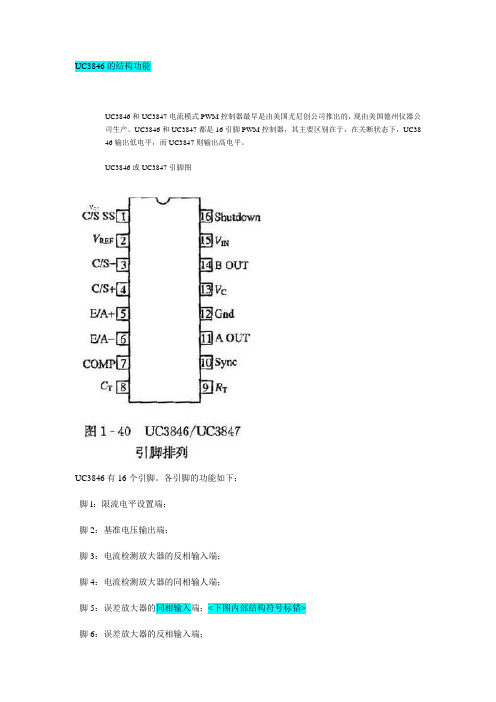
UC3846的结构功能
UC3846和UC3847电流模式PWM控制器最早是由美国尤尼创公司推出的,现由美国德州仪器公司生产。
UC3846和UC3847都是16引脚PWM控制器,其主要区别在于,在关断状态下,UC38 46输出低电平,而UC3847则输出高电平。
UC3846或UC3847引脚图
UC3846有16个引脚。
各引脚的功能如下:
脚l:限流电平设置端;
脚2:基准电压输出端;
脚3:电流检测放大器的反相输入端;
脚4:电流检测放大器的同相输人端;
脚5:误差放大器的同相输入端;<下图内部结构符号标错>
脚6:误差放大器的反相输入端;
脚7:误差放大器反馈补偿;
脚8:振荡器的外接电容端;
脚9:振荡器的外接电阻端;
脚10:同步端;
脚Il:PWM脉冲的A输出端;
脚12:地;
脚13:集电极电源端;
脚14:PwM脉冲的B输出端;
脚15:控制电源输入端;
脚16:关闭端。
UC3846采用标准双列直插式16引脚(DIP—16)封装。
其内部结构框图如图l所示。
UC3846的振荡器频率由外接阻容Rt、CT决定(9脚、8脚)。
CT的充电电流由恒流源所提供。
振荡器的工作频率可按下式近似计算:
式中,Rt一般在1~500 kΩ之间。
为了减小噪声对晶振电容的影响,CT应选择大于100 pF
的电容。
为了防止两路开关管的互通,还要设定两路输出都关断的“死区时间”。
CT上的电压为一个锯齿波.其下降时间即为死区时间
,其死区可设置时间为:
式中,CT增大,锯齿波下降时间(即死区时间)随着增大。
一个初学者对UC3842UC3843开关电源的理解

⼀个初学者对UC3842UC3843开关电源的理解★题外话:作为⼀个初学者,就我个⼈⽽⾔,我最需要的⼊门资料是简答、易懂,最重要的是严谨。
不过,我在⽹上搜集了⼀些资料,总是不令⼈满意,总是不知不觉掉⼊了某⼀个坑⾥,不可⾃拔,因此,⾃⼰总结⼀些资料,⼒求严谨、简答、明了,使后进者避免误区。
由于⾃⼰只是⼀个普通技术⼈员,我很少看含有⼤量数据的计算的资料,更侧重于定性分析,同时,也由于⾃⼰也是初学者,实践经验⽐较少,若有错误,敬请各位指教。
★ UC3842/UC3843开关电源的理解(⼀)UC3842/UC3843开关电源是⾼频开关电源,与低频开关电源相对应。
⾼频开关电源是先把⼯频(50Hz)220VAC先转换为⼏⼗KHz,通过⾼频变压器隔离、降压,得到所需的直流电压。
⽽低频开关电源是直接将50Hz 220VAC通过低频变压器,转换为所需电压。
UC3842/UC3843是电流型PWM开关电源控制器。
先解释⼀下PWM,PWM(Pulse Width Modulation)为脉冲宽度调制,简称脉宽调制,是将模拟信号转换为脉波的⼀种技术,⼀般转换后脉波的周期固定,但脉波的占空⽐会依模拟信号的⼤⼩⽽改变。
PWM技术是⼀种对模拟信号电平的数字编码⽅法,通过使⽤⾼分辨率计数器(调制频率)调制⽅波的占空⽐,从⽽实现对⼀个模拟信号的电平进⾏编码。
其最⼤的优点是从处理器到被控对象之间的所有信号都是数字形式的,⽆需再进⾏数模转换过程;⽽且对噪声的抗⼲扰能⼒也⼤⼤增强(噪声只有在强到⾜以将逻辑值改变时,也可能对数字信号产⽣实质的影响),这也是PWM在通讯等信号传输⾏业得到⼤量应⽤的主要原因。
⽽在开关电源中,脉冲宽度调制(PWM)使⽤的是固定的开关频率(周期),可变的开关导通时间。
低频开关电源现在已经很少了。
低频开关电源就是使⽤⽐较笨重的低频变压器,进⾏降压,⽐如,通过低频变压器,直接把⼯频的220V降到⼯频24V,这就形成了⼀个简单的交流24V电源,如果需要直流24V,只需把⼯频24V经过整流、稳压、滤波,就得到了直流24V电源,也就是低频开关电源。
UC3842的原理及应用详解
UC3842的原理及应用详解
UC3842是一种通用的PWM控制芯片,常用于开关电源中的控制电路。
它采用固定频率、可调宽度的PWM控制方式,可以实现开关电源的过渡型
响应快、稳定性高、效率高的特点。
以下将详细介绍UC3842的原理及应用。
错误放大器用于检测输入电压与参考电压之间的偏差,然后通过比较
器将偏差信号转化为高或低电平。
PWM控制逻辑根据比较器输出的高低电
平产生PWM波形,控制开关管的导通时间。
PWM同步逻辑用于调整PWM波
形的相位,以控制输出电压的稳定性。
S-R锁存器用于存储PWM波形的输
出结果,实现PWM的控制闭环。
时钟和输出驱动电路用于控制PWM波形的
频率和驱动开关管。
1.开关电源控制器:UC3842可以作为开关电源的主要控制芯片,通
过控制PWM波形的宽度和频率,实现开关电源输出电压的稳定。
2.DC-DC变换器:UC3842可以应用于DC-DC变换器中,通过调整PWM
波形的宽度和频率,实现输入电压到输出电压的变换。
3.电力管理系统:UC3842可以应用于电力管理系统中,实现对电压
和电流的精确控制,提高系统的效率和稳定性。
4.能量转换系统:UC3842可以应用于能量转换系统中,实现能量的
高效转换和传输。
5.电动汽车充电器:UC3842可以用于电动汽车充电器的控制电路,
实现对电池充电过程的精确控制和保护。
6.智能家居系统:UC3842可以应用于智能家居系统中的电源控制模块,实现对各种电器设备的高效供电和调控。
uc3846中文资料
UC3846/47电流模式PWM控制器特点和引脚说明1.特点(1)自动前馈补偿。
(2)可编程控制的逐个脉冲限流功能。
(3)推挽输出结构下自动对称校正。
(4)负载响应特性好。
(5)可并连运行,适用于模块系统。
(6)内置差动电流检测放大器,共模输入范围宽。
(7)双脉冲抑制功能。
(8)大电流图腾柱式输出,输出峰值电流500mA。
(9)精密带隙基准电源,精度士1%。
(10)内置欠电压锁定电路。
(11)内置软启动电路。
(12).具有外部关断功能。
(13)工作频率高达500KHz2.引脚说明 UC3846/47采用16引脚(DIL - 16、SOIC-16)和20引脚(PLCC - 20、LCC - 20)两种封装形式。
下面以DIL - 16封装为例进行介绍,其引脚排列如图1—40所示。
UC3846/47的引脚功能简介如下:·C/S SS(引脚1):限流信号/软启动输入端。
该端可接给定信号。
·V REF (引脚2):基准电源输出端。
该端输出一温度特性极佳的基准电压。
·C/S-(引脚3):电流检测比较器反相输入端。
该端接电流检测信号。
·C/S+(引脚4):电流检测比较器正相输入端。
该端接给定信号。
·E/A+(引脚5):误差放大器同相输入端。
在闭环或开环系统中,该端都接给定信号。
·E/A-(引脚6):误差放大器反相输入端。
在闭环系统中,该端接输出反馈信号。
根据需要,可在该端与引脚7之间接入不同功能的反馈网络,构成比例,积分,比例积分等类型的闭环调节器。
在开环系统中,该端直接与7脚相连,构成跟随器。
·COMP(引脚7):误差放大器输出端。
在闭环系统中,根据需要,可在该端与引脚6之间接入不同功能的反馈网络,构成比例,积分,比例积分等类型的闭环调节器。
在开环系统中该端可直接与引脚6相连,构成跟随器。
·C T(引脚8):振荡定时电容接入端。
开关电源用电流模式 PWM 控制器UC3842、UC3843、UC3844、UC3845
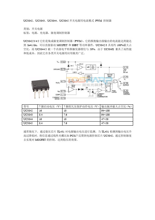
UC3842、UC3843、UC3844、UC3845开关电源用电流模式PWM 控制器
类别:开关电源
标签:电源,充电器,脉宽调制控制器
UC3842/3/4/5它们是集成脉宽调制控制器(PWM),它的推挽输出级输出的电流能达到能达到Io=1.0A,可以直接驱动MOSFET和IGBT等功率器件,UC3842/3具有约100%最大占空比,而UC3844/5被一个内部电平转换触发器钳位与50%,由于UC384X 兼具了高性能和低成本,因此它在各类开关电源用应用极其广泛。
型号7脚启动电压(V)7脚的欠压保护动作电压(V)输出脉冲最大占空比(%)UC3842 16 10 94~100
UC3843 8.4 7.6 94~100
UC3844 16 10 47~50
UC3845 8.4 7.6 47~50
通常情况下,通过稳压芯片TL431对电源输出电压进行监测,当TL431检测到输出电压升高过降低时,将信息通过线性光耦比如PC817反馈到电源控制芯片UC3842,通过控制脉宽去实现对MOSFET的控制,达到稳压的效果。
UC3846脉宽调制高频开关稳压
课程设计说明书题目 UC3846脉宽调制高频开关稳压(院)系电气与信息工程系专业自动化班级学号学生姓名指导老师姓名完成日期 2008 年 6 月 10 日至2008 年 6 月 20 日湖南工程学院课程设计任务书课程名称:电力电子技术题目:UC3846脉宽调制高频开关稳压电源设计专业班级:学生姓名:学号:指导老师:审批:任务书下达日期2008 年6 月10 日设计完成日期2008 年6 月20 日目录第1章概述第2章系统总体方案确定2.1 电路的工作原理2.2 电路的组成第3章主电路设计与分析3.1 主电路的设计3.2 主电路元器件的计算及选型3.3 主电路保护环节的设计第4章控制电路设计与分析4.1 芯片详情4.2功能单元电路的设计4.3控制电路参数确定第5章总结与体会第6章附录总电路图参考文献课程设计评分表第1章概述在电力电子技术的应用及各种电源系统中,开关电源技术均处于核心地位。
对于大型电解电镀电源,传统的电路非常庞大而笨重,如果采用高顿开关电源技术,其体积和重量都会大幅度下降,而且可极大提高电源利用效率、节省材料、降低成本。
在电动汽车和变频传动中,更是离不开开关电源技术,通过开关电源改变用电频率,从而达到近于理想的负载匹配和驱动控制。
高频开关电源技术,更是各种大功率开关电源(逆变焊机、通讯电源、高频加热电源、激光器电源、电力操作电源等)的核心技术。
开关稳压电源(以下简称开关电源)问世后,在很多领域逐步取代了线性稳压电源和晶闸管相控电源。
早期出现的是串联型开关电源,其主电路拓扑与线性电源相仿,但功率晶体管工作于开关状态。
随着脉宽调制(PWM)技术的发展,PWM开关电源问世,它的特点是用20kHz的载波进行脉冲宽度调制,电源的效率可达65%~70%,而线性电源的效率只有30%~40%。
因此,用工作频率为20 kHz的PWM开关电源替代线性电源,可大幅度节约能源,从而引起了人们的广泛关注,在电源技术发展史上被誉为20kHz革命。
电流控制型PWM控制芯片UC3846

摘要:介绍并比较了电压控制型和电流控制型DC/DC变换器的基本原理,设计出了基于电流控制型PWM 控制芯片UC3846的大功率DC/DC变换器的实用电路,提出了两种UC3846输出脉冲封锁方式,设计出一种新颖的IGBT驱动电路,实验结果证明,该电路具有较好的控制特性和稳定性。
关键词:DC/DC变换器;脉宽调制;电压控制型;电流控制型;IGBT驱动0 引言随着工业、航空、航天、军事等应用领域技术的不断发展,人们对开关稳压电源的要求也越来越高。
某系统对大功率开关稳压电源提出的要求是:输入电压为AC220V,输出电压为DC38V,输出电流为100A。
开关电源的结构一般为先进行AC/DC然后再DC/DC的形式,考虑到论文篇幅的限制,仅对DC/DC变换部分进行讨论。
大功率DC/DC变换器主电路拓扑有很多种,诸如双管正激式、推挽式、半桥式和全桥式等。
控制芯片的种类也非常多,主要分为电流控制型与电压控制型两大类。
电压控制型只对输出电压采样,作为反馈信号进行闭环控制,采用PWM技术调节输出电压,从控制理论的角度看,这是一种单环控制系统。
电流控制型是在电压控制型的基础上,增加一个电流负反馈环节,使其成为双环控制系统,从而提高了电源的性能。
根据对各种拓扑和控制方式的技术成熟程度,工程化实现难度,电气性能以及成本等指标的比较,本文选用半桥式DC/DC变换器作为主电路,电流型PWM控制芯片UC3846作为该系统的控制单元。
1 电压控制型脉宽调制器和电流控制型脉宽调制器图1为电压控制型变换器的原理框图。
电源输出电压的采样反馈值V f与参考电压V r进行比较放大,得到误差信号V e,它与锯齿波信号比较后,PWM比较器输出PWM控制信号,经驱动电路驱动开关管通断,产生高频方波电压,由高频变压器传输至副方,经整流滤波得到所需要的电压。
改变电压给定V r,即可改变输出电压V o。
图1 电压控制型的原理图图2为电流控制型变换器的原理框图。
- 1、下载文档前请自行甄别文档内容的完整性,平台不提供额外的编辑、内容补充、找答案等附加服务。
- 2、"仅部分预览"的文档,不可在线预览部分如存在完整性等问题,可反馈申请退款(可完整预览的文档不适用该条件!)。
- 3、如文档侵犯您的权益,请联系客服反馈,我们会尽快为您处理(人工客服工作时间:9:00-18:30)。
Line, Load, and Temperature (Note 2)
Output Noise Voltage
10Hz≤ f ≤10kHz, TJ=25°C (Note 2)
Long Term Stability
TJ=125°C, 1000 Hrs. (Note 2)
Short Circuit Output Current VREF=0V
Output Voltage
TJ=25°C, IO=1mA
Line Regulation
VIN=8V to 40V
Load Regulation
IL=1mA to 10mA
Temperature Stability
Over Operating Range, (Note 2)
Total Output Variation
Common Mode Range
VIN=8V to 40V
Open Loop Voltage Gain ∆VO=1.2 to 3V, VCM=2V
100
100
µV
5
5
mV
-10 -45
-10 -45
mA
2
UC1846/7 UC2846/7 UC3846/7
ELECTRICAL
(Unless otherwise stated, these specifications apply for TA=-55°C to +125°C for UC1846/7; -40°C
• Parallel Operation Capability for Modular Power Systems
“power modules" while maintaining equal current sharing. Protection circuitry includes built-in under-voltage lockout and pro-
UC1846/7; -40°C to +85°C for the UC2846/7; and 0°C to +70°C for the UC3846/7; VIN=15V, RT=10k, CT=4.7nF, TA=TJ.)
PARAMETER
TEST CONDITIONS
Reference Section
UC1846/UC1847 UC2846/UC2847 MIN. TYP. MAX.
UC3846/UC3847 MIN. TYP. MAX. UNITS
5.05 5.10 5.15 5.00 5.10 5.20 V
5
20
5
20 mV
3
15
3
15 mV
0.4
0.4
mV/°C
5.00
5.20 4.95
5.25 V
Note 1. All voltages are with respect to Ground, Pin 13. Currents are positive into, negative out of the speficied terminal. Consult Packaging Section of Databook for thermal limitations and considerations of packages. Pin numbers refer to DIL and SOIC packages only.
CONNECTION DIAGRAMS
DIL-16, SOIC-16 (TOP VIEW) J or N Package, DW Package
PLCC-20, LCC-20 (TOP VIEW) Q, L Packages
UC1846/7 UC2846/7 UC3846/7
PACKAGE PIN FUNCTION
• Double Pulse Suppression
shutdown with automatic restart or latch the supply off.
• 500mA (Peak) Totem-pole Outputs
Other features include fully latched operation, double pulse suppression, deadline adjust capability, and a ±1% trimmed bandgap
• Automatic Symmetry Correction in Push-pull line regulation, enhanced load response characteristics, and a sim-
Configuration
pler, easier-to-design control loop. Topological advantages include
• Programmable Pulse-by-Pulse Current Limiting
features to implement fixed frequency, current mode control schemes while maintaining a minimum external parts count. The superior performance of this technique can be measured in improved
• ±1% Bandgap Reference
reference.
• Under-voltage Lockout • Soft Start Capability
The UC1846 features low outputs in the OFF state, while the UC1847 features high outputs in the OFF state.
CHARACTERISTICS (cont.) to +85°C for the UC2846/7; and 0°C to +70°C for the UC3846/7; VIN=15V, RT=10k, CT=4.7nF,
TA=TJ.)
PARAMETER
TEST CONDITIONS
Oscillator Section
• Enhanced Load Response Characteristics inherent pulse-by-pulse current limiting capability, automatic symmetry correction for push-pull converters, and the ability to parallel
• Differential Current Sense Amplifier with
grammable current limit in addition to soft start capability. A shut-
Wide Common Mode Range
down function is also available which can initiate either a complete
Initial Accuracy
TJ=25°C
Voltage Stability
VIN=8V to 40V
Temperature Stability
Over Operating Range (Note 2)
Sync Output High Level
Sync Output Low Level
Sync Input High Level
FUNCTION
PIN
N/C
1
C/L SS
2
VREF
3
C/S-
4
C/S+
7
E/A-
8
Comp
9
CT
10
N/C
11
RT
12
Sync
13
A Out
14
Gnd
15
N/C
16
VC
17
B Out
18
VIN
19
Shutdown
20
ELECTRICAL CHARACTERISTICS (Unless otherwise stated, these specifications apply for TA=-55°C to +125°C for
• Shutdown Terminal
• 500kHZ Operation
BLOCK DIAGRAM
1/97
ABSOLUTE MAXIMUM RATINGS (Note 1)
Supply Voltage (Pin 15) . . . . . . . . . . . . . . . . . . . . . . . . . . . . . . . . . . . . . . . . . +40V Collector Supply Voltage (Pin 13). . . . . . . . . . . . . . . . . . . . . . . . . . . . . . . . . . +40V Output Current, Source or Sink (Pins 11, 14). . . . . . . . . . . . . . . . . . . . . . . . 500mA Analog Inputs (Pins 3, 4, 5, 6, 16) . . . . . . . . . . . . . . . . . . . . . . . . . . . -0.3V to +VIN Reference Output Current (Pin 2). . . . . . . . . . . . . . . . . . . . . . . . . . . . . . . . . -30mA Sync Output Current (Pin 10) . . . . . . . . . . . . . . . . . . . . . . . . . . . . . . . . . . . . . -5mA Error Amplifier Output Current (Pin 7) . . . . . . . . . . . . . . . . . . . . . . . . . . . . . . -5mA Soft Start Sink Current (Pin 1) . . . . . . . . . . . . . . . . . . . . . . . . . . . . . . . . . . . . 50mA Oscillator Charging Current (Pin 9) . . . . . . . . . . . . . . . . . . . . . . . . . . . . . . . . . 5mA Power Dissipation at TA=25°C . . . . . . . . . . . . . . . . . . . . . . . . . . . . . . . . . 1000mW Power Dissipation at TC=25°C . . . . . . . . . . . . . . . . . . . . . . . . . . . . . . . . . 2000mW Storage Temperature Range . . . . . . . . . . . . . . . . . . . . . . . . . . . . -65°C to +150°C Lead Temperature (soldering, 10 seconds. . . . . . . . . . . . . . . . . . . . . . . . . +300°C