FreescaleMM912J637汽车智能电池传感器(IBS)解决方案
基于智能电池传感器(IBS)的电池管理对未来汽车设计的成功至关重要
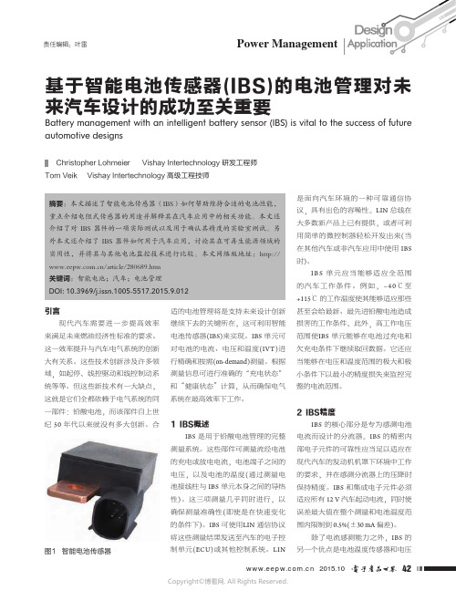
图1 智能电池传感器
传感器全都包含在一个器件中。
因负荷的优先级。
汽车因此能够以合理
的顺序关停这些系统,以提醒驾驶员它甚至允许汽车的舒适系统间歇性地
图2 IBS 细节示例
压。
这些电池单元堆叠中的每一个都
应当包含其自身的电池管理系统,以确保当一个电池单元发生故障时不会忽略的。
例如,一个
在 100 A 电流下只会造成
图3 使用 IBS 的实际起停测试图4 使用 IBS 的实际驾驶测试
布市区。
选择该路线的原因是为了获
得对标准早晨通勤情况的近似,不会中断交通流,也不会使测试被其他驾内布拉斯加州哥伦布市早晨开车上班时的情况的短时模拟
图5 IBS 测量的电流、电压和温度值。
电动汽车能量管理单元电路板自动测试系统
电动汽车能量管理单元电路板自动测试系统
刘奕任;齐铂金;郑敏信
【期刊名称】《计测技术》
【年(卷),期】2016(036)003
【摘要】针对电动汽车能量管理单元其电路板测试繁杂的问题,研究设计一种自动测试系统.采用Frescale MC9 S12系列MCU作为主控芯片,通过CAN总线实现上位机、下位机、被测板之间的数据传输.系统实现了对能量管理单元4种板件及整机的6类不同测试.上位机软件可对测试项目进行高度灵活地配置,实时显示测试结果,保存至数据库,并生成Word报表.经前期测试,对于同一种板件的全功能测试可在1 min内完成,单个通道的绝对误差可小于0.05 V,并且其故障检出率可达到100%.
【总页数】6页(P22-27)
【作者】刘奕任;齐铂金;郑敏信
【作者单位】北京航空航天大学机械工程及自动化学院, 北京100191;北京航空航天大学机械工程及自动化学院, 北京100191;北京航空航天大学机械工程及自动化学院, 北京100191
【正文语种】中文
【中图分类】TB22;TP274.5
【相关文献】
1.混合动力牵引车蓄电池能量管理单元的设计与实验 [J], 郑荣才;朱诗顺;康少华;金涛;李慧梅
2.利用AVS技术与PWI能量管理单元降低系统能耗 [J], Michael
Drake ;Netnarin(Joy) Taylor
3.电动汽车充换电站换电操作管理单元的设计与实现 [J], 胡道栋;张娟;克潇;杨校辉;尹新涛
4.一种应用于低功耗植入式医疗芯片的无线能量管理单元 [J], 夏瑞威;赵亚;高海军
5.就地化保护智能管理单元自动测试系统设计 [J], 张玉中; 浮明军; 李国杰; 匡海燕因版权原因,仅展示原文概要,查看原文内容请购买。
一款适用于汽车的智能电池传感器参考设计
一款适用于汽车的智能电池传感器参考设计
奥地利微电子的智能电池传感器(IBS)设计适用于监测最新磷酸铁
锂汽车电池以及传统AGM(铅酸)电池的电量状况(SOC)以及电池安全状况(SOH)。
IBS 的测量前端采用AS8515,能精确、实时地测量电池的电流和电压、电路板的温度,并将这些数据输出为电子信号。
测量数据由富士通
ARM Cortex-M3 微控制器进行处理,为任何类型的12V 电池带来准确的读数。
具有完整文档且作为开发包中一部分的该参考设计现已提供,随时都可以投入生产,并可能被汽车生产厂商选用作为IBS 系统的现成模板。
与竞争对手提供的固定架构整合系统不同,奥地利微电子的参考设计允许使用者自由地选择微控制器。
奥地利微电子IBS 参考设计提供的软件演示了使用库伦计数方法如何进行SOC 计算,并在电流负载变化超过5A 时如何计算由此引起的电池阻抗。
该软件能轻松地输出到任何开发者选择的微控制器,包括其他的ARM Cortex-M 系列设备。
AS8515 包含一个集成的LIN 收发器以及能在汽车系统中作为LIN 从属设备的IBS 传感器模块。
该参考设计包括一个含有LIN 控制器和USB 控制器的独立LIN 主板,使开发者能通过奥地利微电子的图形用户界面(适用于Windows 操作系统的电脑)控制并配置传感器模块。
IBS 模块结合了奥地利微电子在高精度和高敏感度模拟电路方面的专业知识,能进行极其准确的电池测量:在整个信号范围内电流测量精度误差为。
HOCHIKI ANALOG SENSORS BASES 安装指南说明书
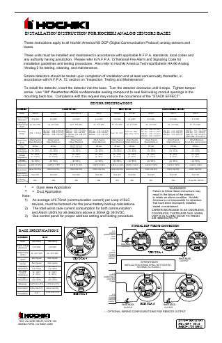
Visual Alarm/ Power Indicator
CO Sensor Response Time
Dual LED N/A
Indoor Use Only Dual LED N/A
Indoor Use Only Dual LED N/A
Indoor Use Only Dual LED N/A
Indoor Use Only Indoor Use Only
) &
) &
350ȝ$7\SLFDO ȝ$0D[LPXP
88 Hex ) &
) &
) &
350ȝ$7\SLFDO ȝ$0D[LPXP
41.0 VDC
41.0 VDC
41.0 VDC
41.0 VDC
24 - 41.0 VDC
24 - 41.0 VDC
24 - 41.0 VDC
24 - 41.0 VDC
300 fpm: 2000 fpm: 4000 fpm:
0.70 - 4.00 %/ft* 0.70 - 3.86 %/ft** 0.70 - 2.65 %/ft**
BASE
Model
YBN-NSA-4
Applied Voltage (Maximum)
41.0 VDC
Operating Voltage Range
(S-SC) Alarm Current
(S-SC)
Remote LED Current Operating
Temperature
UL Listed Ambient Temperature
Current Consumption
(S-SC)
Device Type Code
贝尔金 Conserve Insight 能源使用监测器用户指南说明书

Package ContentsConserve Insight Energy Use Monitor User Guide and Warranty Information1.5 meterCOindicatorcost mode icon unit for COmode icon1 Plug in the Conserve insightThe Conserve Insight screen willshow 0-1.0W until you plug a devicein. If your plugged-in device powerconsumption is below 1.0 watts, the0-1.0W screen will continue to appear.2 Plug any household device into theConserve insightThe screen will automatically displayhow many Pounds per year your devicecosts in its current operating mode. (Youdo not need to press anything on yourConserve Insight to view this screen.)3 Conserve insight buttonsWith your device plugged into theConserve Insight, press one of thecorresponding buttons to enter into thedesired mode. Pressing the CO2 orPound button more than once will switchbetween monthly and yearly readings,which are illustrated by the calendar iconin the bottom right corner of the display(30 for a month and 365 for a year).Estimated CO emissionsassociated with powering theconnected device for month or year1 energy Bar MonitorThe energy bar (located at the center-bottom of the display) tracks the amount of power being used by your connected device. At initial start-up of your Conserve Insight, the energy use is represented by one animated moving bar. After 45 minutes of use, your Conserve Insight will switch to a “Averaging Mode” and the energy use will be represented by three moving bars. Averaging Mode: Your Conserve Insightswitches to this mode after 45 minutes ofuse. Once in this mode, your ConserveInsight can more accurately calculate thecost of your attached device based onyour actual usage. The Conserve Insighttakes continuous readings of your deviceusage throughout the day, both while yourdevice is on and off. The readout will displaypower costs and environmental impact,averaged over time, based on your usage.2 Set rate ModeYour Conserve Insight is programmedwith a preset rate for the cost of electricitybased on the average for your geographicregion, but it may not match exactly to therate you are charged by your specific utilitycompany. In order to get a more accuratecost, you can enter your specific rate bylooking up the kWh rate shown on yourelectricity bill and then adjusting the EnergyUnit Cost per kWh on the Conserve Insight.Programming Set Rate Mode: Any timeduring operation, if the Pound button isheld down for longer than 3 seconds,your Conserve Insight will go into “SetRate Mode.” Once in this mode you canadjust the Energy Unit Cost per kWhto match that of your electricity bill.In “Set Rate Mode,” press the Watts buttonto increase your Energy Unit Cost per kWhand the CO2 button to decrease this cost.Holding down the Pound button for longer than 3 seconds will reset the Energy Unit Cost back to the factory default.To exit “Set Rate Mode,” pressthe Dollar button. If no buttons are pressed for 5 seconds, the display will automatically exit “Set Rate Mode.”3 Set CO2 Conversion Factor Mode(Continued)Enter your CO2 conversion factor in eitherpounds (lbs) CO2 per kilowatt hour, orkilograms (kg) CO2 per kilowatt hour,depending on the unit shown on the display.Change the value used for the CO2conversion factor when you arein “CO2 Conversion Factor Mode” bypressing the Watts button to increase thevalue and the CO2 button to decrease thevalue. Holding down the Dollar buttonfor longer than 3 seconds will reset the CO2conversion factor to the factory default.C hange the weight unit by pressing thePound button in “CO2 Conversion FactorMode.” The weight unit used to display CO2will flash. By pressing the Watts button orCO2 button you can change the weight unit.3 Set CO2 Conversion Factor ModeResidential electricity comes from severaldifferent sources, many of which generatepower by burning fossil fuels that emitCO2 into the atmosphere. Your ConserveInsight monitor comes with a preset CO2conversion factor based on averages foryour geographic region. In order to get amore accurate reading for your area, youcan enter the CO2 conversion factor usingdata from your electricity utility companyor the International Energy Agency (IEA).This will give a more accurate calculation forhow much CO2 emissions are associatedwith powering any connected device.Programming the CO2 Conversion Factor:Any time during operation, if the CO2 buttonis held down for longer than 3 seconds, yourConserve Insight monitor will go into “CO2Conversion Factor Mode.” Once in this mode,you can adjust the CO2 conversion factor.Press the Pound button twice to exit “CO2 Conversion Factor Mode.” If no buttons are pressed for 5 seconds, the display will automatically exit “CO2 Conversion Factor Mode.” L CD display screen3-button control- C O2 Button: EnvironmentalImpact (CO2 emitted to generatepower to run your device)- P ound Button: Cost Impact- W atts Button: Energy Consumption(Watts used by your device)1.5 meter tethered cord betweenoutlet and display unit- E asier viewing of the display unit. Allowsdisplay unit to be placed on a countertop.Easy-to-understand graphic iconsDisplays data in both monthlyand yearly predictionsI nstantaneous and Averagingmodes of usage calculation- I nstantaneous Mode: Values arecalculated using the power beingconsumed at that very moment. Goodfor showing cost and environmentalimpact of the connected devicein various operating modes.- A veraging Mode: Values are calculatedfrom an average of power consumedover the whole time the unit has beenplugged in. This mode allows for betterunderstanding of how connecteddevices affect your monthly bill andtheir true environmental impact.When I plug different devices into my Conserve Insight, after some time, the values on the screen don’t change as much and there is a strange icon above the meter bar. If you leave your Conserve Insight plugged into a wall outlet for more than 45 minutes, it swaps into an averaging mode. This mode is very helpful for getting more accurate estimates of the true cost of the connected device, but if you are just testing lots of different devices and their various operating modes, then the instantaneous mode is most helpful. To revert back to instantaneous mode, unplug the Conserve Insight from the wall outlet and plug it back in again. You will be in instantaneous mode for another 45 minutes. nOte: If you want the display to remain in instantaneous mode, you can do this by holding down the CO2 and Watts buttons simultaneously for 3 seconds. When you see the averaging icon flash, it means you have disabled the averaging function.A description of the different operating modes can be found in the Product Features section of this user guide.Sometimes when I plug devices intoConserve Insight, the screen shows “0-1.0Watt” and I don’t know what it means.Your Conserve Insight uses sensitiveelectronics to measure the amount of powerflowing to your connected device. Whenthe connected device is consuming a verysmall amount of electricity, it becomesvery difficult to distinguish between thepower being consumed and the electricalnoise found at all power outlets. To ensureaccurate readings, the Conserve Insightstops showing values below 1.0 wattsand displays the “0-1.0 Watt” screen.Specifications1.5 meter cord connecting display and socketElectrical Rating: 250V~/13A/50Hz/3250WMaximum Watts Displayed: 3250Maximum Pounds Displayed: 9999Safety informationimportant: Use indoors in a dry location.NOTE: This equipment has been tested and found to comply with the limitsfor a Class B digital device, pursuant to part 15 of the FCC Rules. Theselimits are designed to provide reasonable protection against harmfulinterference in a residential installation. This equipment generates, uses,and can radiate radio frequency energy and, if not installed and usedin accordance with the instructions, may cause harmful interference toradio communications. However, there is no guarantee that interferencewill not occur in a particular installation. If this equipment does causeharmful interference to radio or television reception, which can bedetermined by turning the equipment off and on, the user is encouragedto try to correct the interference by one of the following measures:. R eorient or relocate the receiving antenna.•. I ncrease the separation between the equipment and receiver.•. C onnect the equipment into an outlet on a circuit different•from that to which the receiver is connected.. C onsult the dealer or an experienced radio/TV technician for help.•Belkin International, Inc., is not responsible for any interference causedby unauthorized modifications to this equipment. Such modificationscould void the user’s authority to operate this equipment.Ce Statementnote: This product complies with the essential requirements of the EULow Voltage Directive 2006/95/EC and the EMC Directive 2004/108/EC. A copy of the European Union CE marking "Declaration ofConformity" may be obtained at the website: /DOCBelkin international, inc., limited 2-Year Product Warranty What this warranty covers.Belkin International, Inc.(“Belkin”) warrants to the original purchaser of this Belkin product that the product shall be freeof defects in design, assembly, material, or workmanship.What the period of coverage is.Belkin warrants the Belkin product for two years.What will we do to correct problems?Product Warranty.Belkin will repair or replace, at its option, any defective product free of charge (except for shipping charges for the product).Belkin reserves the right to discontinue any of its products without notice, and disclaims any limited warranty to repair or replace any such discontinued products.In the event that Belkin is unable to repair or replace the product (for example, because it has been discontinued), Belkin will offer either a refund or a credit toward the purchase of another product from Belkin. com in an amount equal to the purchase price of the product as evidenced on the original purchase receipt as discounted by its natural use. What is not covered by this warranty?All above warranties are null and void if the Belkin product is not provided to Belkin for inspection upon Belkin’s request at the sole expenseof the purchaser, or if Belkin determines that the Belkin product has been improperly installed, altered in any way, or tampered with.The Belkin Product Warranty does not protect against acts of God such as flood, lightning, earthquake, war, vandalism, theft, normal-use wear and tear, erosion, depletion, obsolescence, abuse, damage due to low voltage disturbances (i.e.brownouts or sags), non-authorized program, or system equipment modification or alteration THIS WARRANTY CONTAINS THE SOLE WARRANTY OF BELKIN.THERE ARE NO OTHER WARRANTIES, EXPRESSED OR, EXCEPT ASREQUIRED BY LAW, IMPLIED, INCLUDING THE IMPLIED WARRANTYOR CONDITION OF QUALITY, MERCHANTABILITY OR FITNESS FORA PARTICULAR PURPOSE, AND SUCH IMPLIED WARRANTIES, IFANY, ARE LIMITED IN DURATION TO THE TERM OF THIS WARRANTY.IN NO EVENT SHALL BELKIN BE LIABLE FOR INCIDENTAL, SPECIAL,DIRECT, INDIRECT, CONSEQUENTIAL OR MULTIPLE DAMAGESSUCH AS, BUT NOT LIMITED TO, LOST BUSINESS OR PROFITSARISING OUT OF THE SALE OR USE OF ANY BELKIN PRODUCT,EVEN IF ADVISED OF THE POSSIBILITY OF SUCH DAMAGES.This warranty gives you specific legal rights, and you may also have otherrights, which may vary from jurisdiction to jurisdiction. Some jurisdictionsdo not allow the exclusion or limitation of incidental, consequential,or other damages, so the above limitations may not apply to you.Belkin Tech Support/supportFor more information and to learn about otherBelkin Conserve energy management products,please go to /conserve8820uk00554F7C005Facts gathered from a study conducted by the University of Illinois, the International Energy Agency, and the U.S. Environmental Protection Agency.use energy WiselyUsing electricity or driving a car does have an effect on the environment, but by using energy wisely we can prevent waste and reduce carbon dioxide (CO ) emissions.CO is a greenhouse gas that accumulates in the Earth’s atmosphere, trapping heat from the sun and keeping the planet warm. CO comes, in part, from the burning of fossil fuels, such as coal and gasoline, to generate electricity for use in our homes and to power our cars.The amount of CO in our atmosphere has increased over the past century, and the majority of scientists questioned in a recent international study agree that global temperatures have risen dramatically compared with levels from the 1800s, with human activity being a significant contributing factor. According to theInternational Energy Agency, a warmer Earth may lead to changes in rainfall patterns, a rise in sea level, and a wide range of impacts on plants, wildlife, and humans.A good way to visualize CO is to imagine that 1kg of CO would fill up 1566 soda cans (0,35l), or a box 0,8m high, 0,8m wide and 0,8m deep.Belkin Conserve products can help you do your part to use energy wisely.use less, Save More, Feel Good.。
飞思卡尔推出用于汽车电池监控的智能传感器
飞思卡尔推出用于汽车电池监控的智能传感器
飞思卡尔半导体公司
【期刊名称】《电子技术应用》
【年(卷),期】2011(37)6
【摘要】@@ 飞思卡尔半导体公司日前推出了MM912J637智能电池传感器(IBS),它能准确地测量铅酸电池的电压、电流和温度并计算出电池的状态,即使是在恶劣的行车状态下也可完成.随着混合动力车的出现和汽车整体电子内容的增加,以及启停系统的推出,能够准确地评估这些电池参数正在变得越来越重要.
【总页数】2页(P26-27)
【作者】飞思卡尔半导体公司
【作者单位】
【正文语种】中文
【相关文献】
1.飞思卡尔推出用于汽车电池监控的智能传感器 [J], 飞思卡尔半导体公司
2.飞思卡尔推出用于汽车电池监控的智能传感器 [J], 无
3.飞思卡尔推出用于汽车电池监控的智能传感器 [J], 飞思卡尔半导体
4.飞思卡尔推出用于汽车电池监控的智能传感器 [J],
5.飞思卡尔推出用于汽车电池监控的智能传感器 [J],
因版权原因,仅展示原文概要,查看原文内容请购买。
电池电压检测芯片
电池电压检测芯片电池电压检测芯片是一种广泛应用于电池管理系统的集成电路,其主要功能是实时检测和测量电池的电压,并将测量结果通过接口传输给外部设备或者系统。
在电动车、无线通信、便携式电子设备等领域,电池电压检测芯片起着至关重要的作用。
电池电压检测芯片主要由模拟前端电路和数字信号处理电路两部分组成。
模拟前端电路负责将电池的电压信号进行放大、滤波和数字化处理,以便后续的数字信号处理。
数字信号处理电路则负责对模拟信号进行采样、转换、滤波、校准和处理,最终输出准确的电池电压数值。
在电池电压检测芯片中,模拟前端电路起着关键作用。
它通过放大电池电压信号,并进行精确的滤波,以降低噪声的影响,并消除电池电压信号中的直流偏置。
模拟前端电路还包括了一个精确的参考电压源,用于校准和比较电池电压信号。
这些操作保证了电池电压信号的准确性,同时提高了测量的精度和稳定性。
数字信号处理电路在电池电压检测芯片中同样非常重要。
它通过高速的数字信号采样和转换,将模拟信号转换成二进制码,使得后续的处理更为方便和准确。
数字信号处理电路还包括了滤波和校准算法,用于消除数字信号中的噪声和误差。
通过这些处理,电池电压检测芯片可以提供准确的电池电压数值,并及时将数值传输给外部设备或者系统。
除了上述的基本功能,电池电压检测芯片还具备一些其他的特性和功能。
例如,它可以实现多通道的电池电压检测,用于检测和测量多组电池的电压。
它还可以具备温度补偿功能,通过测量电池的温度来补偿电池电压的变化。
此外,一些先进的电池电压检测芯片还可以通过内置的芯片识别电路,识别电池的型号和容量,以便更好地对电池进行管理。
近年来,随着电池技术的不断发展和电子设备的普及,电池电压检测芯片得到了广泛的应用。
通过使用电池电压检测芯片,我们可以实时监测和测量电池的电压,及时获取电池的状态信息,为电子设备的使用和维护提供参考和支持。
同时,电池电压检测芯片还可以提高电池的使用寿命和安全性,减少电池的损耗和故障。
Freescale 34933 双极桥驱动器说明说明书
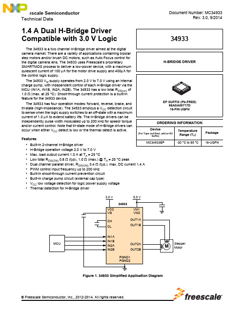
Document Number: MC34933Rev. 3.0, 9/2014Freescale Semiconductor Technical Data© Freescale Semiconductor, Inc., 2012-2014. All rights reserved.1.4 A Dual H-Bridge Driver Compatible with 3.0 V LogicThe 34933 is a two channel H-Bridge driver aimed at the digital camera market. There are a variety of applications containing bipolar step motors and/or brush DC motors, such as Auto Focus control for the digital camera lens. The 34933 uses Freescale's proprietarySMARTMOS process to deliver a low-power device, with a maximum quiescent current of 100 μA for the motor drive supply and 400μA for the control logic supply.The 34933 V M supply operates from 2.0 V to 7.0 V using an internal charge pump, with independent control of each H-Bridge driver via the MCU (IN1A, IN1B, IN2A, IN2B). The 34933 has a low total R DS(on) of 1.0 Ω (max. at 25 °C). Shoot-through current protection is a built-in feature for the 34933 device.The 34933 has four operation modes: forward, reverse, brake, and tri-state (high-impedance). The 34933 employs a V CC detection circuit to sense when the logic supply switches to an off-state with a maximum current of 1.0 μA to extend battery life. The H-Bridge drivers can be independently pulse width modulated up to 200 kHz for speed/ torque and/or current control. Note that tri-state mode of H-Bridge drivers can occur when either V CC detect is low or the thermal detect is active.Features •Built-in 2-channel H-Bridge driver•H-Bridge operation voltage 2.0 V to 7.0 V •Max. load output current 1.0 A at T A = 25 °C•Low total R DS(ON) 0.8 Ω (typ), 1.0 Ω (max.) @ T A = 25 °C peak•Dual channel parallel driver, R DS(ON) 0.4 Ω (typ.). max. DC current 1.4 A •PWM control input frequency up to 200 kHz •Built-in shoot-through current prevention circuit •Built-in charge pump circuit (external cap type)•V CC low voltage detection for logic power supply voltage •Thermal detection for H-Bridge driverFigure 1. 34933 Simplified Application Diagram34933ORDERING INFORMATIONDevice(For Tape and Reel, add an R2Suffix)Temperature Range (T A )Package MC34933EP-20 °C to 85 °C16-UQFNH-BRIDGE DRIVERAnalog Integrated Circuit Device Data34933INTERNAL BLOCK DIAGRAMINTERNAL BLOCK DIAGRAMFigure 2. 34933 Simplified Internal Block DiagramVCC DETECTIONTHERMAL DETECTIONCONTROL LOGICVGCH CLVCCIN1AIN1BIN2AIN2B* VM1 and VM2 are connected internally. Both VM1 and VM2 must be tied together on the PCB.PGND1 and PGND2 are connected internally. Both PGND1 and PGND2 must be tied together on the PCB.CHARGE PUMPVCCVM VG =VM+VCCVCCdetVCCtdetVCCVCCVCCdet tdetLEVEL SHIFTER PRE-DRIVERVCC VGVM1OUT1A OUT1BPGND1VM2OUT2A OUT2BPGND2Low-side DriverHigh-side DriverLow-side DriverHigh-side DriverAnalog Integrated Circuit Device Data 34933PIN CONNECTIONSPIN CONNECTIONSFigure 3. 34933 Pin ConnectionsTable 1. 34933 Pin DefinitionsPin NumberPin Name Pin FunctionFormal Name Definition1OUT1A Output H-Bridge Output 1A Output A of H-Bridge channel 1.2PGND1Power supply Power Ground 1Power supply grounds for the 34933 device. Refer to the application diagram for recommended layout.3PGND2Power supplyPower Ground 2Power supply grounds for the 34933 device. Refer to the application diagram for recommended layout.4OUT2A Output H-Bridge Output 2A Output A of H-Bridge channel 25OUT2B OutputH-Bridge Output 2BOutput B of H-Bridge channel 26VM2Power supply Motor Drive Power Supply 2Power supply pins for the 34933 motor drive circuitry. Refer to the application diagram for recommended layout.7IN2A Input Logic Input Control 2ALogic input control of OUT2A 8IN2B Input Logic Input Control 2B Logic input control of OUT2B 9IN1B Input Logic Input Control 1B Logic input control of OUT1B 10IN1A InputLogic Input Control 1ALogic input control of OUT1A11VCC Power supply Control Logic Power SupplyPower supply for the control logic circuitry.12VG Output Charge Pump OutputCapacitor Charge pump output pin connected to an external capacitor. The V G voltage is the sum of the V CC and V M power supplies.13CL Input/Output Charge Pump Capacitor 1Low-side charge pump capacitor connection 14CH Input/OutputCharge Pump Capacitor 2High-side charge pump capacitor connection15VM1Power supply Motor Drive Power Supply 1Power Supply pins for the 34933 motor drive circuitry. Refer to the application diagram for recommended layout.16OUT1BOutputH-Bridge Output 1BOutput B of H-Bridge channel 117(1)Exposed Pad Power supply EPThe exposed pad is connected to ground plane via the exposed pad solder pad. Note the primary purpose of the exposed pad for 34933 is thermal heat dissipation. Therefore, adequate thermal vias should be included in the PCB design.Notes1.Exposed pad is used as a heat sink. Connect it to the power ground through four thermal vias where the area is wide.U T 1BM 1HLI N 2I N 2V M O U T 2OUT2A PGND2PGND1OUT1AAnalog Integrated Circuit Device Data34933ELECTRICAL CHARACTERISTICS MAXIMUM RATINGSELECTRICAL CHARACTERISTICSMAXIMUM RATINGSTable 2. Maximum RatingsAll voltages are with respect to ground unless otherwise noted. Exceeding these ratings may cause a malfunction or permanent damage to the device.RatingsSymbolValueUnitELECTRICAL RATINGSControl Logic Power Supply Voltage VCC -0.5 to +6.0V Motor Drive Power SupplyVM -0.5 to +7.5V VCC Level Pin Voltage - IN1A, IN1B, IN2A, IN2BVpin1 -0.5 to +5.5V VM Level Pin Voltage - OUT1A, OUT1B, OUT2A, OUT2B, CL Vpin2 -0.5 to +7.5V VM+VCC Level Pin Voltage - CH, VGVpin3 -0.5 to +13.5V Motor Drive Maximum Load Current, T A = 85 °C I LOAD_DC_MD 0.7 A Motor Drive Maximum Load Current, T A = 25 °C I LOAD_DC_MD 1.0 A Motor Drive Maximum Peak Load Current (3)I LOAD_PEAK_MD1.4A Power Dissipation (4)P D 1.0W ESD Voltage (2)Human Body Model (HBM)Machine Model (MM)Charge Device Model (CDM)V ESD±4000±350±1000VTHERMAL RATINGSOperating Temperature Range T A -20 to +85 °C Operating Junction Temperature T J 150 °C Storage Temperature Range T STG-65 to +150°CTHERMAL RESISTANCEThermal Resistance, Junction to Case (5)R θJC 23︒C/W Peak Package Reflow Temperature During Reflow (6), (7)T PPRTNote 7°CNotes 2.ESD testing is performed in accordance with the Human Body Model (HBM) (C ZAP = 100 pF, R ZAP = 1500 Ω), the Machine Model (MM) (C ZAP = 200 pF, R ZAP = 0 Ω), and the Charge Device Model (CDM), Robotic (C ZAP = 4.0 pF).3.Peak time is for 10 ms pulse width at 200 ms intervals. T A = 25°C.4.R θJA = 50 °C/W, in case of 2s2p printed circuit board that defined on SEMI JEDEC JESD51- 3 and JESD51-6.5.Thermal resistance between the die and the case top surface as measured by the cold plate method (MIL SPEC-883 Method 1012.1).6.Pin soldering temperature limit is for 10 seconds maximum duration. Not designed for immersion soldering. Exceeding these limits may cause malfunction or permanent damage to the device.7.Freescale’s Package Reflow capability meets Pb-free requirements for JEDEC standard J-STD-020C. For Peak Package ReflowTemperature and Moisture Sensitivity Levels (MSL), go to , search by part number [e.g. remove prefixes/suffixes and enter the core ID to view all orderable parts. (i.e. MC33xxxD enter 33xxx), and review parametrics.Analog Integrated Circuit Device Data 34933ELECTRICAL CHARACTERISTICSSTATIC AND DYNAMIC ELECTRICAL CHARACTERISTICSSTATIC AND DYNAMIC ELECTRICAL CHARACTERISTICSTable 3. Static and Dynamic Electrical CharacteristicsCharacteristics noted under conditions, VM = 5.0 V, VCC = 3.0 V, unless otherwise noted. Typical values noted reflect the approximate parameter means at T A = 25 °C under nominal conditions, unless otherwise noted.CharacteristicSymbolMinTypMaxUnitPOWER SUPPLYMotor Drive Power Supply Voltage V M 2.0 5.0 7.0V Control Logic Power Supply VoltageV CC 2.73.05.5V Driver Quiescent Supply Current (IN1A, IN1B,IN2A, IN2B = L)No Signal InputI QM-72100uALogic Quiescent Supply Current (IN1A, IN1B, IN2A, IN2B = L)No Signal InputI QVCC-114400uAControl Logic Power Supply Operating Current (IN1A, IN2A = L, IN1B, IN2B = 200kHz)I VCC -350800uA Charge Pump Target VoltageVM = 2.0 V, VCC = 2.7 V, I LOAD = 0A VM = 5.0 V, VCC = 3.0 V, I LOAD = 0A VM = 7.0 V, VCC = 5.5 V, I LOAD = 0A V G4.27.612.04.457.812.34.78.012.5VCharge Pump Wake-up TimeCharge pump is enabled in V CC > V CCDET T VGON-130400usDriver Quiescent Supply Current at VCCDET = L V M = 5.0 V, V CC = 0 VI QM_VCD = L-- 1.0uACharge Pump Switching Frequency F QP -150-kHzH-BRIDGE DRIVERH-Bridge Driver High/Low-side Driver On-Resistance 1V CC = 2.7 V, I SINK = 100 mA, T A = 25 °CR ON1-0.40.45ΩH-Bridge Driver High/Low-side Driver On-Resistance 2 (8)V CC = 2.7 V, I SINK = 700 mA, T A = 25 °CR ON2-0.430.51ΩH-Bridge Driver High/Low-side Driver On-Resistance 3 (8)V CC = 2.7 V, I SINK = 700 mA, T A = 85 °CR ON3-0.510.62ΩH-Bridge Driver High/Low-side Driver On-Resistance 4V CC = 3.0 V, I SINK = 100 mA, T A = 25 °CR ON4-0.390.43ΩH-Bridge Driver High/Low-side Driver On-Resistance 5 (8)V CC = 3.0 V, I SINK = 700 mA, T A = 25 °CR ON5-0.410.48ΩH-Bridge Driver High/Low-side Driver On-Resistance 6 (8)V CC = 3.0 V, I SINK = 700 mA, T A = 85 °CR ON6-0.490.58ΩH-Bridge Driver Output Body Diode Forward Voltage I f = 100 mAV F-0.81.2VInput Pulse Frequency (INA/B)Duty of input signal = 50 %F IN--200kHzNotes8.Guaranteed by designAnalog Integrated Circuit Device Data34933ELECTRICAL CHARACTERISTICSSTATIC AND DYNAMIC ELECTRICAL CHARACTERISTICSH-BRIDGE DRIVER (CONTINUED)H-Bridge Output Propagation Delay Time for OUTA/B (H to L)R LOAD = (1.0 k Ω) between OUTA and OUTB (refer to Figure 4) (IN1A, IN2A = L, IN1B, IN2B = 200 kHz)t PDHL-0.10.5usH-Bridge Output Propagation Delay Time for OUTA/B (L to H)Rload = (1.0 k Ω) between OUTA and OUTB (refer to Figure 4) (IN1A, IN2A = L, IN1B, IN2B = 200 kHz)t PDLH-0.10.5us H-Bridge Output Pulse WidthR LOAD = 20 Ω between OUTA and OUTB, Input Pulse Width = 1.0 μs, 50% to 50%, t PW : 50% to 50% (refer to Figure 5)t PW0.7--usH-Bridge Output Propagation Delay Time (Hi-Z to H) (8)R LOAD = 100 k Ω to 1/2*VM, C LOAD = 0 pF, t PDZH 50% to 75%t PDZH--0.5usH-Bridge Output Propagation Delay- Time (H to Hi-Z) (8)R LOAD = 100 k Ω to 1/2*VM, C LOAD = 0 pF, t PDHZ 75% to 50%t PDHZ-- 2.0usCONTROL LOGICHigh Level Input Voltage (IN1A, IN1B, IN2A, IN2B)V CC = 2.7 V ~ 5.5 VV IHV CC x0.7--VLow Level Input Voltage (IN1A, IN1B, IN2A, IN2B)V CC = 2.7 V ~ 5.5 VV IL--V CC x0.3V High Level Input Current (IN1A, IN1B, IN2A, IN2B)V TERMAINAL1 = 3.0 VI IH9-20uALow Level Input Current (IN1A, IN1B, IN2A, IN2B)V CC = 2.7 V to 5.5 VI IL-1.0--uAInput Pulse Rise Time (IN1A, IN1B, IN2A, IN2B)V CC = 2.7 V to 5.5 Vt R-- 1.0usInput Pulse Fall Time (IN1A, IN1B, IN2A, IN2B)V CC = 2.7 V to 5.5 V t F-- 1.0usDETECTORVCC Detection Voltage (refer to Figure 6)V CCDET 2.0 2.2 2.4V VCC Detection hysteresis Voltage (refer to Figure 6)V CCDETHYS0.050.10.3V Thermal Detection Temperature (9)T DET 150170190°C Thermal Detection Hysteresis Temperature (9)T DETHYS102030°CNotes9.Guaranteed by designTable 3. Static and Dynamic Electrical CharacteristicsCharacteristics noted under conditions, VM = 5.0 V, VCC = 3.0 V, unless otherwise noted. Typical values noted reflect the approximate parameter means at T A = 25 °C under nominal conditions, unless otherwise noted.CharacteristicSymbolMinTypMaxUnitAnalog Integrated Circuit Device Data 34933ELECTRICAL CHARACTERISTICSTIMING DIAGRAMSTIMING DIAGRAMSFigure 4. t PDLH and t PDHL TimingFigure 5. t PW TimingFigure 6 and Figure 7 show the timing charts of input and output signalsTable 4. Truth TableINPUTOUTPUTVccdetTdetIN1A IN2AIN1B IN2B OUT1A OUT2A OUT1B OUT2B L X X X Z Z H L L L L L H L H L H L H L L H L H H L HH Z Z HHXXZZH - High L - LowZ - High-impedanceX - Don’t CareAnalog Integrated Circuit Device Data34933ELECTRICAL CHARACTERISTICS TIMING DIAGRAMSFigure 6. Timing Chart of Input and Output Signal (V CCDET case)Figure 7. Timing Chart of Input and Output Signal (t DET case)Analog Integrated Circuit Device Data 34933FUNCTIONAL DESCRIPTION FUNCTIONAL PIN DESCRIPTIONFUNCTIONAL DESCRIPTIONFUNCTIONAL PIN DESCRIPTIONLOGIC SUPPLY (VCC)The VCC pin carries the logic supply voltage and current into the logic sections of the IC. VCC has an under-voltage threshold. If the supply voltage drops below the under-voltage threshold, the output power stage switches to a tri-state condition. When the supply voltage returns to a level that is above the threshold, the power stage automatically resumes normal operation according to the established condition of the input pins.LOGIC INPUT CONTROL (IN1A, IN1B, IN2A, AND IN2B)These logic input pins control each H-Bridge output. IN1A logic HIGH = OUT1A HIGH. However, if all inputs are HIGH, the output bridges are both tri-stated (refer to Table 4, Truth Table).H-BRIDGE OUTPUT (OUT1A, OUT1B, OUT2A, AND OUT2B)These pins provide connection to the outputs of each of the internal H-Bridges (See Figure 2, 34933 Simplified Internal Block Diagram).MOTOR DRIVE POWER SUPPLY (VM1 AND VM2)The VM pins carry the main supply voltage and current into the power sections of the IC. This supply then becomes controlled and/or modulated by the IC as it delivers the power to the loads attached between the output pins. All VM pins must be connected together on the Printed Circuit Board (PCB).CHARGE PUMP (CL AND CH)These two pins, the CL and CH, connect to the external bucket capacitors required by the internal charge pump. The typical value for the bucket capacitors is 0.1 μF.POWER GROUND (PGND)Power ground pins must be tied together on the PCB and connected to the common ground plane.LOGIC GROUND (EXPOSED PAD)The Exposed Pad is connected to the PCB Ground plane through vias by soldering. Note the primary purpose of the Exposed pad for 34933 is thermal heat dissipation.Therefore, adequate thermal vias should be included in the PCB design. The exposed pad should be connected to the common ground plane.VOLTAGE DETECTION AND THERMAL LIMIT DETECTIONThe 34933 has the VCC Low Voltage Detection (Vccdet) and the Thermal Detection (T DET ). VCC Low Voltage Detec-tion is designed to shutdown of IC functions when VCC becomes lower than specified voltage. Thermal Detection operates when the IC temperature exceeds specified valueand stop H-Bridge operation. Table 5 shows block status of 34933 by each condition. VCC is the control logic power supply for 34933. The system begins to operate when V CC > V CCDET (Typ. 2.2 V).Table 5. Block StatusOperation modeVccdet Tdet Charge PumpH-Bridge Driver1L X Disable Disable 2H L Enable Enable 3HHEnableDisableH - High L - LowX - Don’t CareTYPICAL APPLICATIONTYPICAL APPLICATIONFigure 8 shows a typical application using the 34933. The internal charge pump of this device is powered from the V CC supply. Therefore, care must be taken to ensure V CC is a high enough value to provide sufficient gate-source voltage for the high-side MOSFETs when V M > V CC (e.g., V M = 5.0 V, V CC = 3.0 V), in order to ensure full enhancement of the high-side MOSFET channels.The 34933 can be configured in several applications. The figure below shows the 34933 in a typical Slave Node Application.*1 - It is recommend to use low resistance copper PCB traces betweenVM & VCC ground and the PGND1/PGND2 pins.Figure 8. Typical Application34933Analog Integrated Circuit Device DataAnalog Integrated Circuit Device Data 34933PCB LAYOUTPCB LAYOUTWhen designing a printed circuit board (PCB), connect sufficient capacitance between power supplies (VM & VCC) and ground pins to ensure proper filtering from transients. For all high-current paths, use wide copper traces and theshortest possible distances. Note that capacitors should be placed as close to the 34933 as possible to maximize the filtering capability of each capacitor.Additionally, care must be taken to avoid CEMF spikes induced when inductive currents accumulate at the VM supply. The typical method of snubbing inductive spikes includes connecting a Zener diode or capacitor at the supplypin (VM).Analog Integrated Circuit Device Data34933PACKAGINGPACKAGE DIMENSIONSPACKAGINGPACKAGE DIMENSIONSPackage dimensions are provided in package drawings. To find the most current package outline drawing, go to and perform a keyword search for the drawing’s document number.Table 6.PackageSuffix Package Outline Drawing Number16-PIN UQFNEP98ASA00717DAnalog Integrated Circuit Device Data 34933PACKAGINGPACKAGE DIMENSIONS.Analog Integrated Circuit Device Data34933PACKAGINGPACKAGE DIMENSIONSAnalog Integrated Circuit Device Data 34933PACKAGINGPACKAGE DIMENSIONSAnalog Integrated Circuit Device Data34933REVISION HISTORYREVISION HISTORYREVISIONDATE DESCRIPTION OF CHANGES 2.07/2010•Initial Release.12/2013•No technical changes •Revised back page•Updated document properties 3.09/2014•Changed 98A to 98ASA00717D •Update formatDocument Number: MC34933Rev. 3.09/2014Information in this document is provided solely to enable system and software implementers to use Freescale products. There are no express or implied copyright licenses granted hereunder to design or fabricate any integrated circuits based on the information in this document.Freescale reserves the right to make changes without further notice to any products herein. Freescale makes no warranty, representation, or guarantee regarding the suitability of its products for any particular purpose, nor does Freescale assume any liability arising out of the application or use of any product or circuit, and specifically disclaims any and all liability, including without limitation consequential or incidental damages. “Typical” parameters that may be provided in Freescale data sheets and/or specifications can and do vary in different applications, and actual performance may vary over time. All operating parameters, including “typicals,” must be validated for each customer application by customer’s technical experts. Freescale does not convey any license under its patent rights nor the rights of others. Freescale sells products pursuant to standard terms and conditions of sale, which can be found at the following address: /SalesTermsandConditions .Freescale and the Freescale logo are trademarks of Freescale Semiconductor, Inc., Reg. U.S. Pat. & Tm. Off. SMARTMOS is a trademark of Freescale Semiconductor, Inc. All other product or service names are the property of their respective owners.© 2014 Freescale Semiconductor, Inc.How to Reach Us:Home Page: Web Support:/support。
智能电池电量传感器[实用新型专利]
![智能电池电量传感器[实用新型专利]](https://img.taocdn.com/s3/m/46bb096f83d049649a665890.png)
专利名称:智能电池电量传感器专利类型:实用新型专利
发明人:李秋生
申请号:CN201620249774.2申请日:20160329
公开号:CN205720589U
公开日:
20161123
专利内容由知识产权出版社提供
摘要:本实用新型提供了一种智能电池电量传感器,包括封装件,封装件的外部设置有电流夹、接线柱和接插件,封装件内部设置有分流器,分流器的分流电阻一端与用于连接蓄电池负极的电流夹电连接,分流电阻的另一端与用于连接蓄电池负载负极的接线柱电连接,分流器的输出端与用于连接上级控制单元的接插件电连接。
本实用新型能实时获得蓄电池电量状态同时保证其他电器元件与电池的有效连接。
申请人:李秋生
地址:430056 湖北省武汉市武汉经济技术开发区神龙大道165号
国籍:CN
代理机构:武汉开元知识产权代理有限公司
代理人:俞鸿
更多信息请下载全文后查看。
- 1、下载文档前请自行甄别文档内容的完整性,平台不提供额外的编辑、内容补充、找答案等附加服务。
- 2、"仅部分预览"的文档,不可在线预览部分如存在完整性等问题,可反馈申请退款(可完整预览的文档不适用该条件!)。
- 3、如文档侵犯您的权益,请联系客服反馈,我们会尽快为您处理(人工客服工作时间:9:00-18:30)。
FreescaleMM912J637汽车智能电池传感器(IBS)解决方案
智能电池传感器智能电池传感器智能电池传感器(IBS),支持精密的电流,电压和温度测量,集成的LIN 2.1和LIN2.0接口进行通信,主要用在汽车电池电流/电压/温度监测,电池充电状态监测和电池完好状态监测以及混合动力汽车.本文介绍了MM912J637主要特性,方框图,模拟部分框图以及电流/电压/温度测量通路框图,简化应用电路和所需要外接元件表.Intelligent Integrated Precision Battery SensorThe MM912I637 (96 kB) and MM912J637 (128 kB) are fully integrated LIN Battery monitoring devices, based on Freescale S12 MCU Technology.The device supports precise current measurement via an external shunt resistor, and precise battery voltage measurement via a series resistor directly at the battery plus pole. The integrated temperature sensor combined in the close proximity to the battery, allows battery temperature measurement.The integrated LIN 2.1 interface makes the sensor feedback available on the LIN Bus.MM912J637主要特性:• Battery voltage measurement• Battery current measurement in up to 8 ranges• On chip temperature measurement• Normal and two low-power modes• Current threshold detection and current averaging in standby => wake-up from low-power mode• Triggered wake-up from LIN and periodic wake-up• Signal low pass filtering (current, voltage)• PGA (programmable low-noise gain amplifier) with automatic gain control feature• Accurate internal oscillator (an external quartz oscillator may be used for extended accuracy)• Communication via a LIN 2.1, LIN2.0 bus interface• S12 microcontroller with 128 kByte flash, 6.0 kByte RAM, 4.0 kByte data flash• Background debug module• External temperature sensor option (TSUP, VTEMP)• Optional 2nd external voltage sense input (VOPT)• 4 x 5.0 V GPIO including one Wake-up capable high voltage input (PTB3/L0)• 8 x MCU general purpose I/O including SPI functionality• Industry standard EMC complianceMM912J637目标应用:AutomotiveBattery Current/Voltage/Temperature MonitoringBattery State of Charge MonitoringBattery State of Health MonitoringHybrid Electric Vehicles图1.MM912J637方框图图 2.MM912J637 模拟部分方框图图 3.MM912J637电流测量通路框图图4.MM912J637电压测量通路框图图5.MM912J637温度测量通路框图图6.MM912J637完整通路框图图7.MM912J637 LIN模块框图图8.MM912J637简化应用图图9.MM912J637所需/推荐外接元件所需/推荐外接元件数值表:图10.典型的智能电池传感器(IBS)应用电路(器件GND = 底盘GND)图11.典型的智能电池传感器(IBS)应用电路(器件GND =电池负端)详情请见:/files/analog/doc/data_sheet/MM912_637D1.pdf。
