TIP127_DataSheet
SCDS127A产品说明书

SN74CBT3306CDUAL FET BUS SWITCH5ĆV BUS SWITCH WITH ć2ĆV UNDERSHOOT PROTECTIONSCDS127A − SEPTEMBER 2003 − REVISED OCTOBER 2003D Undershoot Protection for Off-Isolation on A and B Ports Up To −2 VD Bidirectional Data Flow, With Near-Zero Propagation DelayD Low ON-State Resistance (r on )Characteristics (r on = 3 Ω Typical)D Low Input/Output Capacitance Minimizes Loading and Signal Distortion (C io(OFF) = 5 pF Typical)D Data and Control Inputs Provide Undershoot Clamp Diodes D Low Power Consumption (I CC = 3 µA Max)D V CC Operating Range From 4 V to 5.5 V DData I/Os Support 0 to 5-V Signaling Levels (0.8-V, 1.2-V, 1.5-V, 1.8-V, 2.5-V, 3.3-V, 5-V)D Control Inputs Can Be Driven by TTL or 5-V/3.3-V CMOS OutputsD I off Supports Partial-Power-Down Mode OperationD Latch-Up Performance Exceeds 100 mA Per JESD 78, Class IIDESD Performance Tested Per JESD 22− 2000-V Human-Body Model (A114-B, Class II)− 1000-V Charged-Device Model (C101)DSupports Both Digital and AnalogApplications: USB Interface, Bus Isolation,Low-Distortion Signal GatingD OR PW PACKAGE(TOP VIEW)123487651OE 1A 1B GNDV CC 2OE 2B 2Adescription/ordering informationThe SN74CBT3306C is a high-speed TTL-compatible FET bus switch with low ON-state resistance (r on ),allowing for minimal propagation delay. Active Undershoot-Protection Circuitry on the A and B ports of the SN74CBT3306C provides protection for undershoot up to −2 V by sensing an undershoot event and ensuring that the switch remains in the proper OFF state.The SN74CBT3306C is organized as two 1-bit bus switches with separate output-enable (1OE, 2OE) inputs.It can be used as two 1-bit bus switches or as one 2-bit bus switch. When OE is low, the associated 1-bit bus switch is ON, and the A port is connected to the B port, allowing bidirectional data flow between ports. When OE is high, the associated 1-bit bus switch is OFF, and the high-impedance state exists between the A and B ports.ORDERING INFORMATIONT APACKAGE †ORDERABLE PART NUMBER TOP-SIDE MARKING Tube SN74CBT3306CD SOIC − DTape and reel SN74CBT3306CDR CU306C −40°C to 85°CTube SN74CBT3306CPW TSSOP − PWTape and reelSN74CBT3306CPWRCU306C†Package drawings, standard packing quantities, thermal data, symbolization, and PCB design guidelines are available at /sc/package.Copyright 2003, Texas Instruments IncorporatedPlease be aware that an important notice concerning availability, standard warranty, and use in critical applications of Texas Instruments semiconductor products and disclaimers thereto appears at the end of this data sheet.PRODUCTION DATA information is current as of publication date.SN74CBT3306CDUAL FET BUS SWITCH5ĆV BUS SWITCH WITH ć2ĆV UNDERSHOOT PROTECTIONSCDS127A − SEPTEMBER 2003 − REVISED OCTOBER 2003description/ordering information (continued)This device is fully specified for partial-power-down applications using I off . The I off feature ensures that damaging current will not backflow through the device when it is powered down. The device has isolation during power off.To ensure the high-impedance state during power up or power down, OE should be tied to V CC through a pullup resistor; the minimum value of the resistor is determined by the current-sinking capability of the driver.FUNCTION TABLE (each bus switch)INPUT INPUT/OUTPUTOE AFUNCTION L B A port = B port HZDisconnectlogic diagram (positive logic)1A 1OESW1B2A 2OESW2B215736simplified schematic, each FET switch (SW)AEN †B†EN is the internal enable signal applied to the switch.Undershoot Protection CircuitSN74CBT3306CDUAL FET BUS SWITCH5ĆV BUS SWITCH WITH ć2ĆV UNDERSHOOT PROTECTIONSCDS127A − SEPTEMBER 2003 − REVISED OCTOBER 2003 absolute maximum ratings over operating free-air temperature range (unless otherwise noted)†. . . . . . . . . . . . . . . . . . . . . . . . . . . . . . . . . . . . . . . . . . . . . . . . . . . . . . . . . .Supply voltage range, V CC−0.5 V to 7 V Control input voltage range, V IN (see Notes 1 and 2) −0.5 V to 7 V. . . . . . . . . . . . . . . . . . . . . . . . . . . . . . . . . . .. . . . . . . . . . . . . . . . . . . . . . . . . . . . . . . . . .Switch I/O voltage range, V I/O (see Notes 1, 2, and 3) −0.5 V to 7 V. . . . . . . . . . . . . . . . . . . . . . . . . . . . . . . . . . . . . . . . . . . . . . . . . . .Control input clamp current, I IK(V IN< 0) −50 mA. . . . . . . . . . . . . . . . . . . . . . . . . . . . . . . . . . . . . . . . . . . . . . . . . . . . .I/O port clamp current, I I/OK(V I/O< 0) −50 mA ON-state switch current, I I/O (see Note 4) ±128 mA. . . . . . . . . . . . . . . . . . . . . . . . . . . . . . . . . . . . . . . . . . . . . . . . .. . . . . . . . . . . . . . . . . . . . . . . . . . . . . . . . . . . . . . . . .Continuous current through V CC or GND terminals ±100 mA. . . . . . . . . . . . . . . . . . . . . . . . . . . . . . . . . . .Package thermal impedance, θJA (see Note 5):D package 97°C/W. . . . . . . . . . . . . . . . . . . . . . . . . . . . . . . .PW package 149°C/W Storage temperature range, T stg −65°C to 150°C. . . . . . . . . . . . . . . . . . . . . . . . . . . . . . . . . . . . . . . . . . . . . . . . . . .†Stresses beyond those listed under “absolute maximum ratings” may cause permanent damage to the device. These are stress ratings only, and functional operation of the device at these or any other conditions beyond those indicated under “recommended operating conditions” is not implied. Exposure to absolute-maximum-rated conditions for extended periods may affect device reliability.NOTES: 1.All voltages are with respect to ground unless otherwise specified.2.The input and output voltage ratings may be exceeded if the input and output clamp-current ratings are observed.3.V I and V O are used to denote specific conditions for V I/O.4.I I and I O are used to denote specific conditions for I I/O.5.The package thermal impedance is calculated in accordance with JESD 51-7.recommended operating conditions (see Note 6)MIN MAX UNITV CC Supply voltage4 5.5VV IH High-level control input voltage2 5.5VV IL Low-level control input voltage00.8VV I/O Data input/output voltage0 5.5VT A Operating free-air temperature−4085°C NOTE 6:All unused control inputs of the device must be held at V CC or GND to ensure proper device operation. Refer to the TI application report, Implications of Slow or Floating CMOS Inputs, literature number SCBA004.SN74CBT3306CDUAL FET BUS SWITCH5ĆV BUS SWITCH WITH ć2ĆV UNDERSHOOT PROTECTIONSCDS127A − SEPTEMBER 2003 − REVISED OCTOBER 2003electrical characteristics over recommended operating free-air temperature range (unless otherwise noted)PARAMETER TEST CONDITIONS MINTYP †MAX UNIT V IK Control inputs V CC = 4.5 V,I IN = −18 mA−1.8V V IKU Data inputs V CC = 5 V,0 mA > I I ≥ −50 mA,V IN = V CC or GND,Switch OFF−2V I IN Control inputsV CC = 5.5 V,V IN = V CC or GND ±1µA I OZ ‡V CC = 5.5 V,V O = 0 to 5.5 V,V I = 0,Switch OFF,V IN = V CC or GND ±10µA I off V CC = 0,V O = 0 to 5.5 V,V I = 010µA I CC V CC = 5.5 V,I I/O = 0,V IN = V CC or GND,Switch ON or OFF3µA ∆I CC §Control inputs V CC = 5.5 V,One input at 3.4 V,Other inputs at V CC or GND2.5mA C in Control inputs V IN = 3 V or 0 3.5pF C io(OFF)V I/O = 3 V or 0,Switch OFF,V IN = V CC or GND 5pF C io(ON)V I/O = 3 V or 0,Switch ON,V IN = V CC or GND 12.5pFV CC = 4 V,TYP at V CC = 4 VV I = 2.4 V,I O = −15 mA 812on ¶V I O = 64 mA 36r V I = 0I O = 30 mA36ΩCC = 4.5 VV I = 2.4 V,I O = −15 mA 510V IN and I IN refer to control inputs. V I , V O , I I , and I O refer to data pins.†All typical values are at V CC = 5 V (unless otherwise noted), T A = 25°C.‡For I/O ports, the parameter I OZ includes the input leakage current.§This is the increase in supply current for each input that is at the specified voltage level, rather than V CC or GND.¶Measured by the voltage drop between the A and B terminals at the indicated current through the switch. ON-state resistance is determined by the lower of the voltages of the two (A or B) terminals.switching characteristics over recommended operating free-air temperature range (unless otherwise noted) (see Figure 3)FROM TO V CC = 4 V V CC = 5 V ± 0.5 V PARAMETER(INPUT)(OUTPUT)MINMAX MINMAX UNITt pd # A or B B or A 0.240.15ns t en OE A or B 4.6 1.5 4.2ns t disOEA or B4.31.5 4.3ns #The propagation delay is the calculated RC time constant of the typical ON-state resistance of the switch and the specified load capacitance,when driven by an ideal voltage source (zero output impedance).SN74CBT3306CDUAL FET BUS SWITCH5ĆV BUS SWITCH WITH ć2ĆV UNDERSHOOT PROTECTIONSCDS127A − SEPTEMBER 2003 − REVISED OCTOBER 2003undershoot characteristics (see Figures 1 and 2)PARAMETERTEST CONDITIONSMIN TYP †MAXUNIT V OUTU V CC = 5.5 V,Switch OFF,V IN = V CC or GND2V OH −0.3V†All typical values are at V CC = 5 V (unless otherwise noted), T A = 25°C.Figure 1. Device Test Setup50 ΩV SV CC11 V 100 k Ω100 k Ω10 pFDUTInputGeneratorAxBxFigure 2. Transient Input Voltage (V I ) and OutputVoltage (V OUTU ) Waveforms(Switch OFF)−2 V5.5 V10 %20 ns10 %90 %90 %2 ns2 nsV OH − 0.3V OHOutput (V OUTU )Input (Open Socket)SN74CBT3306CDUAL FET BUS SWITCH5ĆV BUS SWITCH WITH ć2ĆV UNDERSHOOT PROTECTIONSCDS127A − SEPTEMBER 2003 − REVISED OCTOBER 2003PARAMETER MEASUREMENT INFORMATIONV OH V OLC L(see Note A)TEST CIRCUITS17 VOpen GNDR LR Lt PLH t PHLOutput Waveform 1S1 at 7 V (see Note B)Output Waveform 2S1 at Open (see Note B)t PZLt PZHt PLZt PHZ 3 V0 V V OH V OL0 VV OL + V ∆V OH − V ∆0 VOutput Control (V IN )3 V3.5 VVOLTAGE WAVEFORMSPROPAGATION DELAY TIMES (t pd(s))VOLTAGE WAVEFORMS ENABLE AND DISABLE TIMESOutputNOTES: A.C L includes probe and jig capacitance.B.Waveform 1 is for an output with internal conditions such that the output is low except when disabled by the output control.Waveform 2 is for an output with internal conditions such that the output is high except when disabled by the output control.C.All input pulses are supplied by generators having the following characteristics: PRR ≤10 MHz, Z O = 50 Ω, t r ≤2.5 ns, t f ≤2.5 ns.D.The outputs are measured one at a time with one transition per measurement.E.t PLZ and t PHZ are the same as t dis .F.t PZL and t PZH are the same as t en .G.t PLH and t PHL are the same as t pd(s). The tpd propagation delay is the calculated RC time constant of the typical ON-stateresistance of the switch and the specified load capacitance, when driven by an ideal voltage source (zero output impedance).H.All parameters and waveforms are not applicable to all devices.1.5 V1.5 V1.5 V1.5 V1.5 V 1.5 V1.5 V1.5 V50 ΩV G1V CCDUT50 ΩV IN50 ΩV G250 ΩV ITEST R L S1V ∆C L 5 V ±0.5 V4 V V CC V I t PHZ /t PZHt PLZ /t PZL t pd(s) 5 V ±0.5 V4 V5 V ±0.5 V4 VOpen Open 7 V 7 V Open Open500 Ω500 Ω500 Ω500 Ω500 Ω500 ΩV CC or GND V CC or GNDGND GND V CC V CC 50 pF 50 pF 50 pF 50 pF 50 pF 50 pF0.3 V 0.3 V 0.3 V 0.3 VOutput Control (V IN )Input GeneratorInput GeneratorV OFigure 3. Test Circuit and Voltage WaveformsPACKAGING INFORMATION(1) The marketing status values are defined as follows:ACTIVE: Product device recommended for new designs.LIFEBUY: TI has announced that the device will be discontinued, and a lifetime-buy period is in effect.NRND: Not recommended for new designs. Device is in production to support existing customers, but TI does not recommend using this part in a new design.PREVIEW: Device has been announced but is not in production. Samples may or may not be available.OBSOLETE: TI has discontinued the production of the device.(2) RoHS: TI defines "RoHS" to mean semiconductor products that are compliant with the current EU RoHS requirements for all 10 RoHS substances, including the requirement that RoHS substance do not exceed 0.1% by weight in homogeneous materials. Where designed to be soldered at high temperatures, "RoHS" products are suitable for use in specified lead-free processes. TI may reference these types of products as "Pb-Free".RoHS Exempt: TI defines "RoHS Exempt" to mean products that contain lead but are compliant with EU RoHS pursuant to a specific EU RoHS exemption.Green: TI defines "Green" to mean the content of Chlorine (Cl) and Bromine (Br) based flame retardants meet JS709B low halogen requirements of <=1000ppm threshold. Antimony trioxide based flame retardants must also meet the <=1000ppm threshold requirement.(3) MSL, Peak Temp. - The Moisture Sensitivity Level rating according to the JEDEC industry standard classifications, and peak solder temperature.(4) There may be additional marking, which relates to the logo, the lot trace code information, or the environmental category on the device.(5) Multiple Device Markings will be inside parentheses. Only one Device Marking contained in parentheses and separated by a "~" will appear on a device. If a line is indented then it is a continuation of the previous line and the two combined represent the entire Device Marking for that device.(6) Lead finish/Ball material - Orderable Devices may have multiple material finish options. Finish options are separated by a vertical ruled line. Lead finish/Ball material values may wrap to two lines if the finish value exceeds the maximum column width.Important Information and Disclaimer:The information provided on this page represents TI's knowledge and belief as of the date that it is provided. TI bases its knowledge and belief on information provided by third parties, and makes no representation or warranty as to the accuracy of such information. Efforts are underway to better integrate information from third parties. TI has taken andAddendum-Page 1continues to take reasonable steps to provide representative and accurate information but may not have conducted destructive testing or chemical analysis on incoming materials and chemicals. TI and TI suppliers consider certain information to be proprietary, and thus CAS numbers and other limited information may not be available for release.In no event shall TI's liability arising out of such information exceed the total purchase price of the TI part(s) at issue in this document sold by TI to Customer on an annual basis.Addendum-Page 2TAPE AND REEL INFORMATION*All dimensions are nominalDevicePackage Type Package Drawing Pins SPQReel Diameter (mm)Reel Width W1(mm)A0(mm)B0(mm)K0(mm)P1(mm)W (mm)Pin1Quadrant SN74CBT3306CDR SOIC D 82500330.012.4 6.4 5.2 2.18.012.0Q1SN74CBT3306CPWR TSSOP PW 82000330.012.47.0 3.6 1.68.012.0Q1SN74CBT3306CPWRTSSOPPW82000330.012.47.03.61.68.012.0Q1*All dimensions are nominalDevice Package Type Package Drawing Pins SPQ Length(mm)Width(mm)Height(mm) SN74CBT3306CDR SOIC D8*******.5336.125.0 SN74CBT3306CPWR TSSOP PW82000367.0367.035.0SN74CBT3306CPWR TSSOP PW82000364.0364.027.0TUBE*All dimensions are nominalDevice Package NamePackage TypePins SPQ L (mm)W (mm)T (µm)B (mm)SN74CBT3306CD D SOIC 87550783940 4.32SN74CBT3306CPWPWTSSOP815053010.236003.5PACKAGE MATERIALS INFORMATION5-Jan-2022PACKAGE OUTLINESOIC - 1.75 mm max heightD0008ASMALL OUTLINE INTEGRATED CIRCUITNOTES:1. Linear dimensions are in inches [millimeters]. Dimensions in parenthesis are for reference only. Controlling dimensions are in inches. Dimensioning and tolerancing per ASME Y14.5M.2. This drawing is subject to change without notice.3. This dimension does not include mold flash, protrusions, or gate burrs. Mold flash, protrusions, or gate burrs shall not exceed .006 [0.15] per side.4. This dimension does not include interlead flash.5. Reference JEDEC registration MS-012, variation AA.EXAMPLE BOARD LAYOUTSOIC - 1.75 mm max heightD0008ASMALL OUTLINE INTEGRATED CIRCUITNOTES: (continued)6. Publication IPC-7351 may have alternate designs.7. Solder mask tolerances between and around signal pads can vary based on board fabrication site.EXAMPLE STENCIL DESIGNSOIC - 1.75 mm max heightD0008ASMALL OUTLINE INTEGRATED CIRCUITNOTES: (continued)8. Laser cutting apertures with trapezoidal walls and rounded corners may offer better paste release. IPC-7525 may have alternate design recommendations.9. Board assembly site may have different recommendations for stencil design.PACKAGE OUTLINETSSOP - 1.2 mm max heightPW0008ASMALL OUTLINE PACKAGENOTES:1. All linear dimensions are in millimeters. Any dimensions in parenthesis are for reference only. Dimensioning and tolerancing per ASME Y14.5M.2. This drawing is subject to change without notice.3. This dimension does not include mold flash, protrusions, or gate burrs. Mold flash, protrusions, or gate burrs shall not exceed 0.15 mm per side.4. This dimension does not include interlead flash. Interlead flash shall not exceed 0.25 mm per side.5. Reference JEDEC registration MO-153, variation AA.EXAMPLE BOARD LAYOUT PW0008ATSSOP - 1.2 mm max heightSMALL OUTLINE PACKAGE ArrayNOTES: (continued)6. Publication IPC-7351 may have alternate designs.7. Solder mask tolerances between and around signal pads can vary based on board fabrication site.EXAMPLE STENCIL DESIGN PW0008ATSSOP - 1.2 mm max heightSMALL OUTLINE PACKAGE ArrayNOTES: (continued)8. Laser cutting apertures with trapezoidal walls and rounded corners may offer better paste release. IPC-7525 may have alternatedesign recommendations.9. Board assembly site may have different recommendations for stencil design.IMPORTANT NOTICE AND DISCLAIMERTI PROVIDES TECHNICAL AND RELIABILITY DATA (INCLUDING DATA SHEETS), DESIGN RESOURCES (INCLUDING REFERENCE DESIGNS), APPLICATION OR OTHER DESIGN ADVICE, WEB TOOLS, SAFETY INFORMATION, AND OTHER RESOURCES “AS IS” AND WITH ALL FAULTS, AND DISCLAIMS ALL WARRANTIES, EXPRESS AND IMPLIED, INCLUDING WITHOUT LIMITATION ANY IMPLIED WARRANTIES OF MERCHANTABILITY, FITNESS FOR A PARTICULAR PURPOSE OR NON-INFRINGEMENT OF THIRD PARTY INTELLECTUAL PROPERTY RIGHTS.These resources are intended for skilled developers designing with TI products. You are solely responsible for (1) selecting the appropriate TI products for your application, (2) designing, validating and testing your application, and (3) ensuring your application meets applicable standards, and any other safety, security, regulatory or other requirements.These resources are subject to change without notice. TI grants you permission to use these resources only for development of an application that uses the TI products described in the resource. Other reproduction and display of these resources is prohibited. No license is granted to any other TI intellectual property right or to any third party intellectual property right. TI disclaims responsibility for, and you will fully indemnify TI and its representatives against, any claims, damages, costs, losses, and liabilities arising out of your use of these resources.TI’s products are provided subject to TI’s Terms of Sale or other applicable terms available either on or provided in conjunction with such TI products. TI’s provision of these resources does not expand or otherwise alter TI’s applicable warranties or warranty disclaimers for TI products.TI objects to and rejects any additional or different terms you may have proposed.Mailing Address: Texas Instruments, Post Office Box 655303, Dallas, Texas 75265Copyright © 2022, Texas Instruments Incorporated。
IQS127 Datasheet CN v1.5
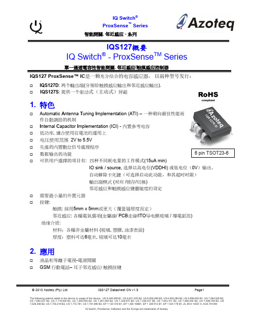
IQ Switch® ProxSense™ Series
智能開關, 邻近感应 - 系列
5. IQS127D 特色
IQS127D依据感应讯号的强度,区分出触摸感应或邻近感应, 并由两个IO口输出。 POUT pin:
IQS127D
o
能夠設定為以下的功用 Active ,主动 Latch, 锁存
电压使用范围 2V to 5.5V 先進的內置數位信号處理程序 6 pin TSOT23-6 数据输出的功能 可供用戶選擇的项目有: 四种不同耗电量的工作模式(15uA min) IO sink / source, 选择以高电位(VDDHI) 或低电位(0V)输出。 自动解除卡死鍵(可选择启动此功能,和其超时时限) 輸出端模式 (对应 /锁存/切换) 邻近感应和触摸感应键靈敏度的设定 需要最小量的外置元器 按键: 触摸: 採用5mm x 5mm或更大(覆蓋層厚度而定) 邻近感应: 各種電氣選項(金屬線/ PCB走線/ITO导电膜玻璃 / 導電鋁箔) 绝缘介质: 材料:各種非金屬材料 (玻璃, 塑膠, 油漆表面) 厚度:塑料可达6毫米, 玻璃可达10毫米
IQ Switch® ProxSense™ Series
智能開關, 邻近感应 - 系列
冰箱, 洗衣機, 辦公室設備, 玩具, 卫生潔具和電器 无火花,适合在危險環境中作人機接口設備 AirButton® (邻近感应)的侦测,可用于背光启动。 待機唤醒的應用 替代机电式開關 Find-In-The-Dark (FITD): 暗中找尋的應用 汽车應用 (例如 : 触摸/ 邻近感应按键用在车內部的燈)
TOUT 1 VSS 2 P OUT 3
6 CX 5 VDDHI 4 V REG
ST TIP122FP TIP127FP 数据手册
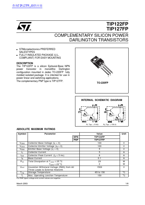
TIP122FP TIP127FPCOMPLEMENTARY SILICON POWERDARLINGTON TRANSISTORSsSTMicroelectronics PREFERRED SALESTYPESsFULLY INSULATED PACKAGE (PLIANT) FOR EASY MOUNTINGDESCRIPTION The TIP122FP is a silicon Epitaxial-Base NPN power transistor in monolithic Darlington configuration mounted in Jedec TO-220FP fully molded isolated package. It is intented for use in power linear and switching applications.The complementary PNP type is TIP127FP.March 2003 ABSOLUTE MAXIMUM RATINGS®1/6查询TIP127FP_03供应商THERMAL DATAELECTRICAL CHARACTERISTICS (T case = 25 oC unless otherwise specified)For PNP types voltage and current values are negative.Safe Operating AreaDerating CurveTIP122FP / TIP127FPDC Current Gain (NPN type)Collector Emitter Saturation Voltage (NPN type)Base Emitter Saturation Voltage (NPN type)DC Current Gain (PNP type)Collector Emitter Saturation Voltage (PNP type)Base Emitter Saturation Voltage (PNP type)TIP122FP / TIP127FPBase Emitter On Voltage (NPN type)Freewheel Diode Forward Voltage (NPN type)Base Emitter On Voltage (PNP type)Freewheel Diode Forward Voltage (PNP type)Switching Time Resistive Load (NPN type)Switching Time resistive Load (PNP type)TIP122FP / TIP127FPTIP122FP / TIP127FPInformation furnished is believed to be accurate and reliable. However, STMicroelectronics assumes no responsibility for the consequences of use of such information nor for any infringement of patents or other rights of third parties which may result from its use. No license is granted by implication or otherwise under any patent or patent rights of STMicroelectronics. Specification mentioned in this publication are subject to change without notice. This publication supersedes and replaces all information previously supplied. STMicroelectronics products are not authorized for use as critical components in life support devices or systems without express written approval of STMicroelectronics.The ST logo is a trademark of STMicroelectronics © 2003 STMicroelectronics – Printed in Italy – All Rights ReservedSTMicroelectronics GROUP OF COMPANIESAustralia - Brazil - Canada - China - Finland - France - Germany - Hong Kong - India - Israel - Italy - Japan - Malaysia - Malta - Morocco - Singapore - Spain - Sweden - Switzerland - United Kingdom - United States.TIP122FP / TIP127FP。
TIP123中文资料
2
1
元器件交易网
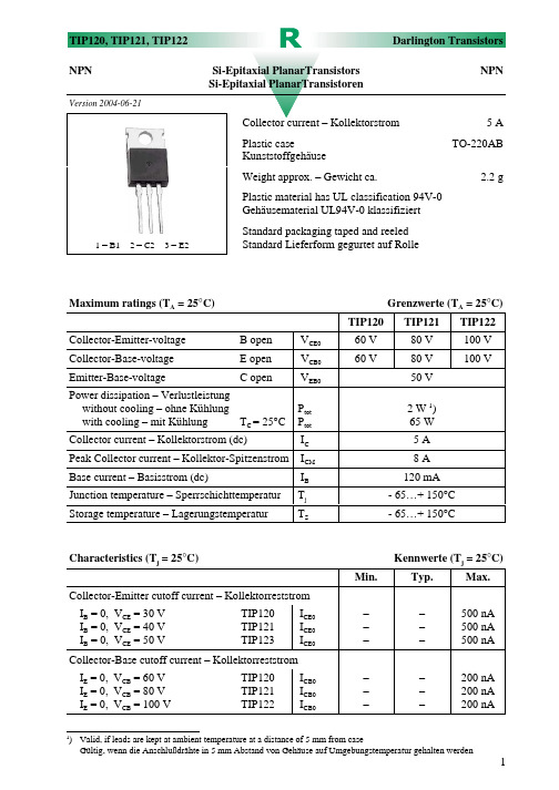
Darlington Transistors TIP120, TIP121, TIP122
Characteristics (Tj = 25°C) Min. Emitter-Base cutoff current – Emitterreststrom IC = 0, VEB = 5 V IC = 3 A, IB = 12 mA IC = 5 A, IB = 20 mA IC = 3 A, VCE = 3 V VCE = 3 V, IC = 0.5 A VCE = 3 V, IC = 3 A VCE = 4 V, IC = 3 A, f = 1 MHz VCB = 10 V, IE = ie = 0, f = 100 kHz Thermal resistance – Wärmewiderstand junction to ambient air – Sperrschicht zu umgebender Luft junction to case – Sperrschicht zu Gehäuse Admissible torque for mounting Zulässiges Anzugsdrehmoment Recommended complementary PNP transistors Empfohlene komplementäre PNP-Transistoren Equivalent Circuit – Ersatzschaltbild IEB0 VCEsat VCEsat VBEon hFE hFE hfe CCB0 – – – – 1000 1000 4 –
Kennwerte (Tj = 25°C) Typ. – – – – – – – – RthA RthC M4 Max. 2 mA 2V 4V 2.5 V – – – 200 pF 62.5 K/W 2) 2 K/W 9 ± 10% lb.in. 1 ± 10% Nm
TIP50;TIP49;TIP48;中文规格书,Datasheet资料

Tamb ≤ 25 oC Storage Temperature Max. Operating Junction Temperature
October 1999
TIP47 350 250
Value
TIP48 TIP49
VCE = 10 V VCE = 10 V
fT
Transition Frequency VCE = 10 V
f = 2 MHz
IC = 0.2 A
hfe
Small Signal Current VCE = 10 V
Gain
f = 1 KHz
∗ Pulsed: Pulse duration = 300 µs, duty cycle ≤ 2 %
VCE(sat)* Collector-Emitter Saturation Voltage
IC = 1 A
IB = 0.2 A
VBE(on)* Base-Emitter Voltage IC = 1 A
VCE = 10 V
hFE* DC Current Gain
IC = 0.3 A IC = 1 A
TIP47 / TIP48 / TIP49 / TIP50
MIN. 4.40 1.23 2.40
0.49 0.61 1.14 1.14 4.95 2.4 10.0
13.0 2.65 15.25 6.2 3.5 3.75
TO-220 MECHANICAL DATA
mm TYP. 1.27
16.4
MAX. 4.60 1.32 2.72
VCE = 150 V VCE = 200 V VCE = 250 V VCE = 300 V
LED电平表 可改音频频谱显示

②软连接法: 使用导线、铜线、跳线、剪下来的电阻腿等任意导体,将两板之间相邻的连接器连接在一起。同样只连接上 面提到的7对连接器。 (两种方法各有利弊:硬连接法操作简单,但需要细心,连接时要尽可能保持所有板子在同一平面上,利于 以后往器材上固定,且连接之后不能受太大扭曲力否则有损坏连接处的可能;软连接法焊接比较麻烦,但板间相 对位置更自由,甚至可以把多个扩展板安装在器材的一个曲面上,尽情发挥无限创意。缺点是接下来的装配过程 中注意不要频繁弯折连接处,避免导线折断)
3、把那种双排座的脚拔掉(很容易拔的),用来定位 LED,可以使 LED 很整齐。 4、LED 间最好自己另加隔光措施,效果会更好,可以用黑色记号笔把所有 LED 侧面涂黑。或者把不透光的 纸粘在 LED 之间等。 5、板子是硬画的,没弄什么网络表。模拟部分走线尽量一点接地。数字部分尽量最短走线。 6、安装固定螺丝时需要在板子两面垫绝缘的垫片,因为设计太紧凑,走线和螺丝孔距离太近。 7、每个扩展板上的 LM3914的 MODE 脚交给它的上一位扩展板来控制,能最优利用板子空间。 8、每个扩展板都预留了4053的位置,但每三个扩展板装一个即可,其余的空着不装 ================================================================================================= 板子到了,开始安装:(以双40段为例) 准备工作: 1、需要烙铁、松香、焊锡等基本工具,要求有一定的焊功,烙铁最好接地。 2、需要万用表(最好是数字的),档次无要求,830都可以,但要熟练基本使用。 3、带着充足的信心及平和的心态。 4、释放身上的静电,可以摸接地的金属机箱、水管等 模块概况:由一块主板(正方形)和若干块扩展板(长方形)组成。把他们连接在一起并适当的设置跳线, 装好元件,就能实现带峰值保持的电平指示。每个扩展板增加双10段显示。 第一大步:将主板和扩展板连接在一起: 1、把所有的 pcb 带有“JAGGY STUDIO”字样的面面向自己,并把主板放在最左边,扩展板依次向右排列, 排成一横行,准备连接。
CW1274 Datasheet说明书

CW1274 4~7节电池保护IC功能特性●过充电保护•阈值范围3.650V、3.850V、4.175V~4.350V,25mV步进,±25mV精度●过放电保护•阈值范围2.300V~2.800V,100mV步进,±30mV精度●放电过流保护•过流检测1阈值范围0.050V~0.100V,±5mV精度•过流检测2阈值范围0.100V~0.200 V,,±10mV精度•短路保护阈值范围0.200V~0.500V,±20mV精度●充电过流保护•阈值范围-0.010V~-0.050V,±5mV精度●温度检测功能充放电高低温保护,温度外部可设●均衡功能●断线检测功能●负载检测功能●级联功能●低功耗设计•工作状态20μA (25°C)•休眠状态5μA (25°C)●封装形式:SSOP24应用领域●吸尘器●电动工具●电动自行车●后备电源●锂离子及锂聚合物电池包基本描述CW1274系列产品是一款高度集成的4~7串锂离子电池或锂聚合物电池保护芯片。
CW1274为电池包提供过充、过放、充放电过流、断线、充放电过温保护以及均衡功能,并支持芯片级联使用。
CW1274 典型应用框图CW1274产品选择指南CW1274 X X X X封装形式,S: SSOP24参数类型,从A到Z电池类型,L:代表锂离子电池F:代表磷酸铁锂电池功能和版本信息,从A 到Z产品目录CW1274 引脚排列图CW1274CW1274 绝对最大额定值注意:绝对最大额定值是指无论在任何条件下都不能超过的额定值。
如果超过此额定值,有可能造成产品损伤。
ESD等级额定工作电压CW1274电气特性除特殊说明外T A=25°CCW1274*2充放电温度保护温度取决于不同电阻的设定,放电低温保护温度默认为充电过温保护温度-20℃,即充电低温保护温度为0℃,则放电低温保护温度为-20℃*3所有过电流保护(包括过流1,过流2和短路保护)解除延迟时间均为60msCW1274原理框图CW1274 功能描述正常状态所有电池电压处于过充检测电压(V OC)和过放检测电压(V OD)之间,且CS端子电压处于过流检测电压(V EC1)和充电过流检测电压(V COC)之间时,CW1274处于正常工作状态。
TIP131;TIP131G;TIP132G;中文规格书,Datasheet资料
DUTY CYCLE, D = t1/t2
0.5 1.0 2.0
5.0 10 20
t, TIME (ms)
Figure 3. Thermal Response
50 100 200
500 1.0 k
r(t), TRANSIENT THERMAL RESISTANCE (NORMALIZED)
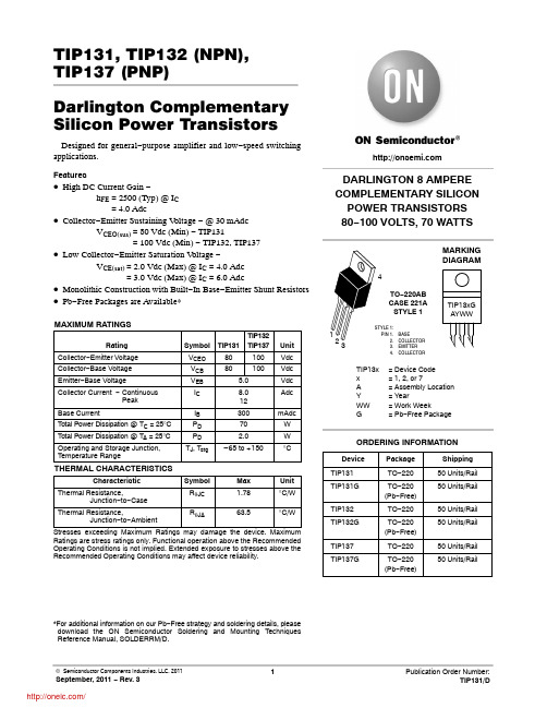
BASE COLLECTOR EMITTER COLLECTOR
TIP13xG AYWW
TIP13x x A Y WW G
= Device Code = 1, 2, or 7 = Assembly Location = Year = Work Week = Pb−Free Package
ORDERING INFORMATION
DARLINGTON 8 AMPERE COMPLEMENTARY SILICON
POWER TRANSISTORS 80−100 VOLTS, 70 WATTS
MARKING DIAGRAM
4
1 2 3
220AB CASE 221A
STYLE 1
STYLE 1: PIN 1. 2. 3. 4.
IB PD PD TJ, Tstg
300 70 2.0 – 65 to + 150
mAdc W W °C
THERMAL CHARACTERISTICS
Characteristic
Symbol
Max
Unit
Thermal Resistance, Junction−to−Case
RqJC
1.78
°C/W
--- 2.04
STYLE 1: PIN 1. BASE 2. COLLECTOR 3. EMITTER 4. COLLECTOR
国光亮光绿色LED设备数据手册说明书

DESCRIPTIONThe Green source color devices are made with Gallium Phosphide Green Light Emitting DiodeFEATURESLow power consumptionPopular T-1 diameter package General purpose leads Reliable and ruggedLong life - solid state reliability Available on tape and reel RoHS compliantAPPLICATIONSStatus indicator IlluminatorSignage applicationsDecorative and entertainment lightingCommercial and residential architectural lightingPACKAGE DIMENSIONSWP710A10GDT-1 (3mm) Solid State LampNotes:1. All dimensions are in millimeters (inches).2. Tolerance is ±0.25(0.01") unless otherwise noted.3. Lead spacing is measured where the leads emerge from the package.4. The specifications, characteristics and technical data described in the datasheet are subject to change without prior notice.Notes:1. θ1/2 is the angle from optical centerline where the luminous intensity is 1/2 of the optical peak value.2. Luminous intensity / luminous flux: +/-15%.3. Luminous intensity value is traceable to CIE127-2007 standards.ParameterSymbol Value Unit Power Dissipation P D 62.5 mW Reverse Voltage V R 5 V Junction Temperature T j 110 °C Operating Temperature T op -40 To +85 °C Storage Temperature T stg -40 To +85°C DC Forward Current I F 25 mA Peak Forward CurrentI FM [1]140 mA Electrostatic Discharge Threshold (HBM) -8000 V Thermal Resistance (Junction / Ambient) R th JA [2] 680 °C/W Thermal Resistance (Junction / Solder point) R th JS [2]460°C/WLead Solder Temperature [3] 260°C For 3 Seconds Lead Solder Temperature [4]260°C For 5 SecondsABSOLUTE MAXIMUM RATINGS at T A =25°CELECTRICAL / OPTICAL CHARACTERISTICS at T A =25°CParameterSymbol Emitting ColorValue Unit Typ. Max. Wavelength at Peak Emission I F = 10mA λpeak Green 565 - nm Dominant Wavelength I F = 10mA λdom [1] Green 568 - nm Spectral Bandwidth at 50% Φ REL MAX I F = 10mA ∆λ Green 30 - nm CapacitanceC Green 15 - pF Forward Voltage I F = 10mA V F [2] Green 2 2.4 V Reverse Current (V R = 5V) I R Green - 10 µA Temperature Coefficient of λpeak I F = 10mA, -10°C ≤ T ≤ 85°C TC λpeak Green 0.1 - nm/°C Temperature Coefficient of λdom I F = 10mA, -10°C ≤ T ≤ 85°C TC λdom Green 0.06 - nm/°C Temperature Coefficient of V F I F = 10mA, -10°C ≤ T ≤ 85°CTC VGreen-2-mV/°CNotes:1. The dominant wavelength (λd) above is the setup value of the sorting machine. (Tolerance λd : ±1nm. )2. Forward voltage: ±0.1V.3. Wavelength value is traceable to CIE127-2007 standards.4. Excess driving current and / or operating temperature higher than recommended conditions may result in severe light degradation or premature failure.Notes:1. 1/10 Duty Cycle, 0.1ms Pulse Width.2. R t h JA ,R t h JS Results from mounting on PC board FR4 (pad size ≥ 16 mm 2 per pad).3. 2mm below package base.4. 5mm below package base.5. Relative humidity levels maintained between 40% and 60% in production area are recommended to avoid the build-up of static electricity – Ref JEDEC/JESD625-A and JEDEC/J-STD-033.TECHNICAL DATAGREENRECOMMENDED WAVE SOLDERING PROFILENotes:1. Recommend pre-heat temperature of 105°C or less (as measured with a thermocoupleattached to the LED pins) prior to immersion in the solder wave with a maximum solder bath temperature of 260°C2. Peak wave soldering temperature between 245°C ~ 255°C for 3 sec (5 sec max).3. Do not apply stress to the epoxy resin while the temperature is above 85°C.4. Fixtures should not incur stress on the component when mounting and during soldering process.5. SAC 305 solder alloy is recommended.6. No more than one wave soldering pass.PACKING & LABEL SPECIFICATIONSPRECAUTIONSStorage conditions1. Avoid continued exposure to the condensing moisture environment and keep the product away from rapid transitions in ambient temperature.2. LEDs should be stored with temperature ≤ 30°C and relative humidity < 60%.3. Product in the original sealed package is recommended to be assembled within 72 hours of opening. Product in opened package for more than a week should be baked for 30 (+10/-0) hours at 85 ~ 100°C.2. When soldering wires to the LED, each wire joint should be separately insulated with heat-shrink tube to prevent short-circuit contact. Do not bundle both wires in one heat shrink tube to avoid pinching the LED leads. Pinching stress on the LED leads may damage the internal structures and cause failure.3. Use stand-offs (Fig.1) or spacers (Fig.2) to securely position the LED above the PCB.4. Maintain a minimum of 3mm clearance between the base of the LED lens and the first lead bend (Fig. 3 ,Fig. 4).5. During lead forming, use tools or jigs to hold the leads securely so that the bending force will not be transmitted to the LED lens and its internal structures. Do not perform lead forming once the component has been mounted onto the PCB. (Fig. 5 )LED Mounting Method1. The lead pitch of the LED must match the pitch of the mounting holes on the PCB during component placement.Lead-forming may be required to insure the lead pitch matches the hole pitch.Refer to the figure below for proper lead forming procedures.Note 1-3: Do not route PCB trace in the contact area between the leadframe and the PCB to prevent short-circuits." ○" Correct mounting method " x " Incorrect mounting methodLead Forming Procedures1. Do not bend the leads more than twice. (Fig. 6 )2. During soldering, component covers and holders should leaveclearance to avoid placing damaging stress on the LED during soldering.(Fig. 7)3. The tip of the soldering iron should never touch the lens epoxy.4. Through-hole LEDs are incompatible with reflow soldering.5. If the LED will undergo multiple soldering passes or face otherprocesses where the part may be subjected to intense heat,please check with Kingbright for compatibility.PRECAUTIONARY NOTES1. The information included in this document reflects representative usage scenarios and is intended for technical reference only.2. The part number, type, and specifications mentioned in this document are subject to future change and improvement without notice. Before production usage customer should refer tothe latest datasheet for the updated specifications.3. When using the products referenced in this document, please make sure the product is being operated within the environmental and electrical limits specified in the datasheet. Ifcustomer usage exceeds the specified limits, Kingbright will not be responsible for any subsequent issues.4. The information in this document applies to typical usage in consumer electronics applications. If customer's application has special reliability requirements or have life-threateningliabilities, such as automotive or medical usage, please consult with Kingbright representative for further assistance.5. The contents and information of this document may not be reproduced or re-transmitted without permission by Kingbright.6. All design applications should refer to Kingbright application notes available at https:///ApplicationNotes。
TIP102;中文规格书,Datasheet资料
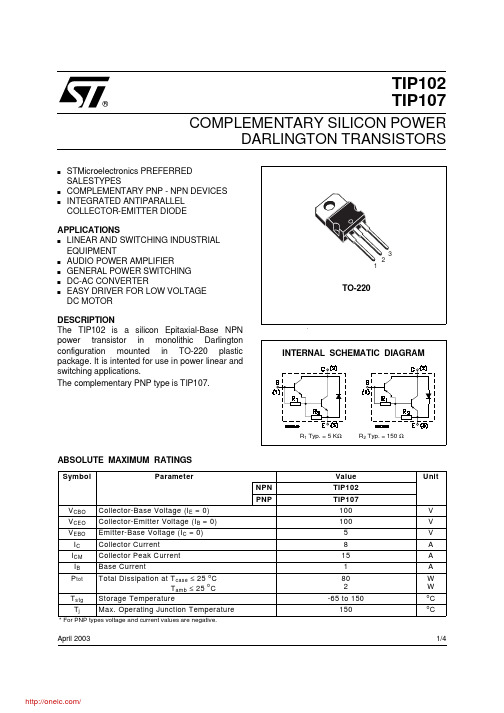
TIP102TIP107COMPLEMENTARY SILICON POWERDARLINGTON TRANSISTORSsSTMicroelectronics PREFERRED SALESTYPESs COMPLEMENTARY PNP - NPN DEVICES sINTEGRATED ANTIPARALLEL COLLECTOR-EMITTER DIODEAPPLICATIONS s LINEAR AND SWITCHING INDUSTRIAL EQUIPMENTs AUDIO POWER AMPLIFIERs GENERAL POWER SWITCHING s DC-AC CONVERTERs EASY DRIVER FOR LOW VOLTAGE DC MOTOR DESCRIPTION The TIP102 is a silicon Epitaxial-Base NPN power transistor in monolithic Darlington configuration mounted in TO-220 plastic package. It is intented for use in power linear and switching applications.The complementary PNP type is TIP107.®April 2003 ABSOLUTE MAXIMUM RATINGS1/4THERMAL DATAELECTRICAL CHARACTERISTICS (T case = 25 oC unless otherwise specified)For PNP types voltage and current values are negative.Safe Operating AreaTIP102 / TIP107TIP102 / TIP107Information furnished is believed to be accurate and reliable. However, STMicroelectronics assumes no responsibility for the consequences of use of such information nor for any infringement of patents or other rights of third parties which may result from its use. No license is granted by implication or otherwise under any patent or patent rights of STMicroelectronics. Specification mentioned in this publication are subject to change without notice. This publication supersedes and replaces all information previously supplied. STMicroelectronics products are not authorized for use as critical components in life support devices or systems without express written approval of STMicroelectronics.The ST logo is a trademark of STMicroelectronics © 2003 STMicroelectronics – Printed in Italy – All Rights ReservedSTMicroelectronics GROUP OF COMPANIESAustralia - Brazil - Canada - China - Finland - France - Germany - Hong Kong - India - Israel - Italy - Japan - Malaysia - Malta - Morocco - Singapore - Spain - Sweden - Switzerland - United Kingdom - United States.TIP102 / TIP107分销商库存信息: STMTIP102。
TIP106G;TIP100G;TIP101G;TIP107G;TIP102;中文规格书,Datasheet资料

50 Units / Rail 50 Units / Rail
50 Units / Rail 50 Units / Rail
50 Units / Rail 50 Units / Rail
50 Units / Rail 50 Units / Rail
RqJA
62.5
°C/W
Stresses exceeding Maximum Ratings may damage the device. Maximum Ratings are stress ratings only. Functional operation above the Recommended Operating Conditions is not implied. Extended exposure to stresses above the Recommended Operating Conditions may affect device reliability. 1. IC = 1.1 A, L = 50 mH, P.R.F. = 10 Hz, VCC = 20 V, RBE = 100 W
TA TC 4.0 80
PD, POWER DISSIPATION (WATTS)
3.0 60
TC 2.0 40
/
1.0 20 TA
00 0
20 40 60 80 100 120 140 160 T, TEMPERATURE (°C)
Figure 2. Power Derating
DARLINGTON 8 AMPERE COMPLEMENTARY SILICON
POWER TRANSISTORS 60−80−100 VOLTS, 80 WATTS
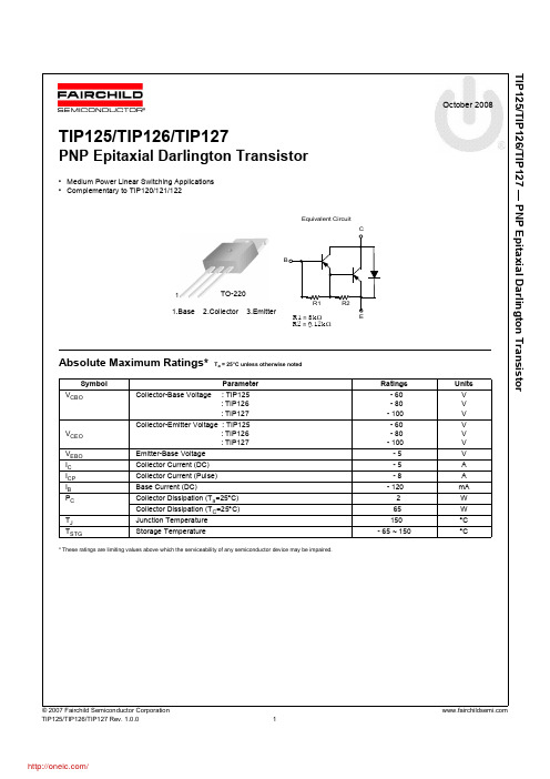
TIP127;TIP125TU;TIP127TU;TIP126TU;TIP125;中文规格书,Datasheet资料
V CBO Collector-Base Voltage : TIP125: TIP126: TIP127 - 60- 80- 100VVVV CEO Collector-Emitter Voltage : TIP125: TIP126: TIP127- 60- 80- 100VVVV EBO Emitter-Base Voltage - 5V I C Collector Current (DC) - 5A I CP Collector Current (Pulse) - 8A I B Base Current (DC) - 120mA P C Collector Dissipation (T a=25°C) 2W Collector Dissipation (T C=25°C) 65W T J Junction Temperature 150°C T STG Storage Temperature- 65 ~ 150°C* These ratings are limiting values above which the serviceability of any semiconductor device may be impaired.TIP125/TIP126/TIP127 PNP Epitaxial Darlington TransistorTIP125/TIP126/TIP127Rev. I31TRADEMARKSThe following are registered and unregistered trademarks and service marks Fairchild Semiconductor owns or is authorized to use andis not intended to be an exhaustive list of all such trademarks.DISCLAIMERFAIRCHILD SEMICONDUCTOR RESERVES THE RIGHT TO MAKE CHANGES WITHOUT FURTHER NOTICE TO ANY PRODUCTS HEREIN TO IMPROVE RELIABILITY, FUNCTION, OR DESIGN. FAIRCHILD DOES NOT ASSUME ANY LIABILITY ARISING OUT OF THE APPLICATION OR USE OF ANY PRODUCT OR CIRCUIT DESCRIBED HEREIN; NEITHER DOES IT CONVEY ANY LICENSE UNDER ITS PATENT RIGHTS, NOR THE RIGHTS OF OTHERS. THESE SPECIFICATIONS DO NOT EXPAND THE TERMS OF FAIRCHILD’S WORLDWIDE TERMS AND CONDITIONS, SPECIFICALLY THE WARRANTY THEREIN, WHICH COVERS THESE PRODUCTS.LIFE SUPPORT POLICYFAIRCHILD’S PRODUCTS ARE NOT AUTHORIZED FOR USE AS CRITICAL COMPONENTS IN LIFE SUPPORT DEVICES OR SYSTEMS WITHOUT THE EXPRESS WRITTEN APPROVAL OF FAIRCHILD SEMICONDUCTOR CORPORATION.As used herein:1. Life support devices or systems are devices or systemswhich, (a) are intended for surgical implant into the body, or (b) support or sustain life, and (c) whose failure to perform when properly used in accordance with instructions for use provided in the labeling, can be reasonably expected to result in significant injury to the user.2.A critical component is any component of a life support device or system whose failure to perform can be reasonably expected to cause the failure of the life support device or system, or to affect its safety or effectiveness.PRODUCT STATUS DEFINITIONS Definition of Terms ACEx ®Build it Now™CorePLUS™CROSSVOLT ™CTL™Current Transfer Logic™EcoSPARK ®Fairchild ®Fairchild Semiconductor ®FACT Quiet Series™FACT ®FAST ®FastvCore™FPS™FRFET ®Global Power Resource SMGreen FPS™Green FPS™ e-Series™GTO™i-Lo ™IntelliMAX™ISOPLANAR™MegaBuck™MICROCOUPLER™MicroFET™MicroPak™MillerDrive™Motion-SPM™OPTOLOGIC ®OPTOPLANAR ®®PDP-SPM™Power220®Power247®POWEREDGE ®Power-SPM™PowerTrench ®Programmable Active Droop™QFET ®QS™QT Optoelectronics™Quiet Series™RapidConfigure™SMART START™SPM ®STEALTH™SuperFET™SuperSOT™-3SuperSOT™-6SuperSOT™-8SyncFET™The Power Franchise ®TinyBoost™TinyBuck™TinyLogic ®TINYOPTO™TinyPower™TinyPWM™TinyWire™µSerDes™UHC ®UniFET™VCX™Datasheet Identification Product Status DefinitionAdvance InformationFormative or In DesignThis datasheet contains the design specifications for product development. Specifications may change in any manner without notice.Preliminary First ProductionThis datasheet contains preliminary data; supplementary data will be pub-lished at a later date. Fairchild Semiconductor reserves the right to make changes at any time without notice to improve design.No Identification Needed Full ProductionThis datasheet contains final specifications. Fairchild Semiconductor reserves the right to make changes at any time without notice to improve design. Obsolete Not In ProductionThis datasheet contains specifications on a product that has been discontin-ued by Fairchild semiconductor. The datasheet is printed for reference infor-mation only.分销商库存信息:FAIRCHILDTIP127TIP125TU TIP127TU TIP126TU TIP125TIP126。
TIP142中文资料
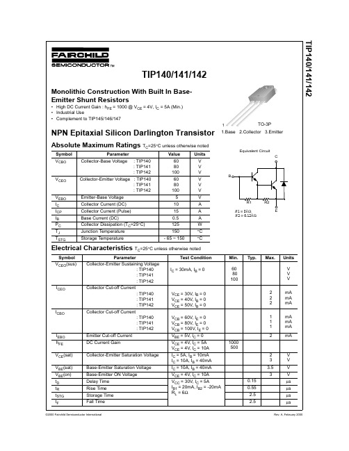
TIP140/141/142TIP140/141/142TIP140/141/142TRADEMARKSThe following are registered and unregistered trademarks Fairchild Semiconductor owns or is authorized to use and is not intended to be an exhaustive list of all such trademarks.ACEx™Bottomless™CoolFET™CROSSVOLT™E2CMOS™FACT™FACT Quiet Series™FAST®FASTr™GTO™HiSeC™ISOPLANAR™MICROWIRE™POP™PowerTrench®QFET™QS™Quiet Series™SuperSOT™-3SuperSOT™-6SuperSOT™-8SyncFET™TinyLogic™UHC™VCX™DISCLAIMERFAIRCHILD SEMICONDUCTOR RESERVES THE RIGHT TO MAKE CHANGES WITHOUT FURTHER NOTICE TO ANY PRODUCTS HEREIN TO IMPROVE RELIABILITY, FUNCTION OR DESIGN. FAIRCHILD DOES NOT ASSUME ANY LIABILITY ARISING OUT OF THE APPLICATION OR USE OF ANY PRODUCT OR CIRCUIT DESCRIBED HEREIN; NEITHER DOES IT CONVEY ANY LICENSE UNDER ITS PATENT RIGHTS, NOR THE RIGHTS OF OTHERS.LIFE SUPPORT POLICYFAIRCHILD’S PRODUCTS ARE NOT AUTHORIZED FOR USE AS CRITICAL COMPONENTS IN LIFE SUPPORT DEVICES OR SYSTEMS WITHOUT THE EXPRESS WRITTEN APPROVAL OF FAIRCHILD SEMICONDUCTOR INTERNATIONAL.As used herein:1. Life support devices or systems are devices or systems which, (a) are intended for surgical implant into the body, or (b) support or sustain life, or (c) whose failure to perform when properly used in accordance with instructions for use provided in the labeling, can be reasonably expected to result in significant injury to the user.2. A critical component is any component of a life support device or system whose failure to perform can be reasonably expected to cause the failure of the life support device or system, or to affect its safety or effectiveness.PRODUCT STATUS DEFINITIONSDefinition of TermsDatasheet Identification Product Status DefinitionAdvance Information Formative or InDesign This datasheet contains the design specifications for product development. Specifications may change in any manner without notice.Preliminary First Production This datasheet contains preliminary data, andsupplementary data will be published at a later date.Fairchild Semiconductor reserves the right to makechanges at any time without notice in order to improvedesign.No Identification Needed Full Production This datasheet contains final specifications. FairchildSemiconductor reserves the right to make changes atany time without notice in order to improve design. Obsolete Not In Production This datasheet contains specifications on a productthat has been discontinued by Fairchild semiconductor.The datasheet is printed for reference information only.。
FAIRCHILD TIP125 126 127 DATA SHEET
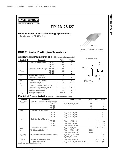
现货库存、技术资料、百科信息、热点资讯,精彩尽在鼎好!TIP125/126/127PNP Epitaxial Darlington TransistorAbsolute Maximum Ratings T C =25°C unless otherwise notedElectrical Characteristics T C =25°C unless otherwise noted* Pulse Test : PW ≤300µs, Duty cycle ≤2%Symbol ParameterValue Units V CBOCollector-Base Voltage : TIP125: TIP126 : TIP127 - 60 - 80 - 100V V V V CEO Collector-Emitter Voltage : TIP125: TIP126 : TIP127 - 60 - 80 - 100V V V V EBO Emitter-Base Voltage - 5V I C Collector Current (DC) - 5A I CP Collector Current (Pulse) - 8A I B Base Current (DC)- 120mA P CCollector Dissipation (T a =25°C) 2W Collector Dissipation (T C =25°C)65W T J Junction Temperature 150°C T STGStorage Temperature- 65 ~ 150°CSymbol ParameterTest ConditionMin.Max.Units V CEO (sus)Collector-Emitter Sustaining Voltage: TIP125: TIP126: TIP127I C = -100mA, I B = 0-60 -80-120V V V I CEOCollector Cut-off Current: TIP125: TIP126: TIP127 V CE = -30V, I B = 0 V CE = -40V, I B = 0 V CE = -50V, I B = 0 -2 -2 -2mA mA mA I CBOCollector Cut-off Current: TIP125: TIP126: TIP127 V CB = -60V, I E = 0 V CB = -80V, I E = 0 V CB = -100V, I E = 0 -1 -1 -1mA mA mA I EBO Emitter Cut-off Current V BE = -5V, I C = 0 -2mAh FE* DC Current GainV CE = -3V, I C = 0.5A V CE = -3V, I C = -3A 10001000V CE (sat)* Collector-Emitter Saturation Voltage I C = -3A, I B = -12mA I C =-5A, I B =-20mA -2 -4V V V BE (on)* Base-Emitter ON Voltage V CE = -3V, I C = -3A-2.5V C obOutput CapacitanceV CB = -10V, I E = 0, f = 0.1MHz300pFTIP125/126/127Medium Power Linear Switching Applications•Complementary to TIP120/121/122Equivalent CircuitBECR1R2R 18k Ω≅R 20.12k Ω≅1.Base 2.Collector 3.Emitter1TO-220TIP125/126/127TIP125/126/127DISCLAIMERFAIRCHILD SEMICONDUCTOR RESERVES THE RIGHT TO MAKE CHANGES WITHOUT FURTHER NOTICE TO ANY PRODUCTS HEREIN TO IMPROVE RELIABILITY, FUNCTION OR DESIGN. FAIRCHILD DOES NOT ASSUME ANY LIABILITY ARISING OUT OF THE APPLICATION OR USE OF ANY PRODUCT OR CIRCUIT DESCRIBED HEREIN;NEITHER DOES IT CONVEY ANY LICENSE UNDER ITS PATENT RIGHTS, NOR THE RIGHTS OF OTHERS.LIFE SUPPORT POLICYFAIRCHILD’S PRODUCTS ARE NOT AUTHORIZED FOR USE AS CRITICAL COMPONENTS IN LIFE SUPPORT DEVICES OR SYSTEMS WITHOUT THE EXPRESS WRITTEN APPROVAL OF FAIRCHILD SEMICONDUCTOR CORPORATION.As used herein:TRADEMARKSThe following are registered and unregistered trademarks Fairchild Semiconductor owns or is authorized to use and is not intended to be an exhaustive list of all such trademarks.1. Life support devices or systems are devices or systems which, (a) are intended for surgical implant into the body,or (b) support or sustain life, or (c) whose failure to performwhen properly used in accordance with instructions for useprovided in the labeling, can be reasonably expected to result in significant injury to the user.2. A critical component is any component of a life support device or system whose failure to perform can bereasonably expected to cause the failure of the life support device or system, or to affect its safety or effectiveness.PRODUCT STATUS DEFINITIONS Definition of TermsDatasheet Identification Product Status DefinitionAdvance InformationFormative or In Design This datasheet contains the design specifications for product development. Specifications may change in any manner without notice.PreliminaryFirst ProductionThis datasheet contains preliminary data, andsupplementary data will be published at a later date.Fairchild Semiconductor reserves the right to make changes at any time without notice in order to improve design.No Identification Needed Full ProductionThis datasheet contains final specifications. Fairchild Semiconductor reserves the right to make changes at any time without notice in order to improve design.Obsolete Not In ProductionThis datasheet contains specifications on a product that has been discontinued by Fairchild semiconductor.The datasheet is printed for reference information only.A CEx™Bottomless™CoolFET™CROSSVOLT ™DenseTrench™DOME™EcoSPARK™E 2CMOS™EnSigna™FACT™FACT Quiet Series™FAST ®FASTr™FRFET™GlobalOptoisolator™GTO™HiSeC™ISOPLANAR™LittleFET™MicroFET™MICROWIRE™OPTOLOGIC™OPTOPLANAR™PACMAN™POP™Power247™PowerTrench ®QFET™QS™QT Optoelectronics™Quiet Series™SLIENT SWITCHER ®SMART START™STAR*POWER™Stealth™SuperSOT™-3SuperSOT™-6SuperSOT™-8SyncFET™TruTranslation™TinyLogic™UHC™UltraFET ®VCX™STAR*POWER is used under license。
TIP122TIP127功率达林顿晶体管

TIP122/TIP127功率达林顿晶体管一、产品简介TIP122和TIP127是两款高性能的功率达林顿晶体管,广泛应用于大电流驱动场合。
它们具有高电流增益、高电压和电流容量,适用于工业控制、电源管理、电动机驱动等领域。
二、产品特点1. 高电流增益:TIP122和TIP127具有高达1000的电流增益,能够轻松驱动大电流负载。
2. 高电压和电流容量:TIP122的集电极发射极电压为100V,集电极电流为5A;TIP127的集电极发射极电压为60V,集电极电流为3A。
3. 互补输出:TIP122为NPN型,TIP127为PNP型,两者可搭配使用,实现互补输出。
4. 内置快速恢复二极管:TIP122和TIP127内置快速恢复二极管,用于保护晶体管免受反电动势损害。
5. 封装类型:TO220塑料封装,便于安装和散热。
三、应用领域1. 电动机驱动:TIP122和TIP127可用于驱动各种类型的电动机,如直流电动机、步进电动机等。
2. 电源管理:在开关电源、线性电源等电源管理电路中,TIP122和TIP127可用于控制大电流开关。
3. 工业控制:适用于各种工业控制场合,如自动化设备、等。
4. 照明控制:用于调光器、镇流器等照明控制电路。
四、使用注意事项1. 正确接线:确保集电极、发射极和基极的接线正确,避免因接线错误导致器件损坏。
3. 防止反电动势损害:在感性负载场合,务必在晶体管输出端并联一个续流二极管,以防止反电动势损害晶体管。
4. 电压和电流限制:请勿超过TIP122和TIP127的最大集电极发射极电压和集电极电流,以确保器件长期稳定运行。
五、电路设计指南1. 基极驱动电路:设计合适的基极驱动电路至关重要,因为它决定了晶体管的开关速度和效率。
确保驱动电流足够,以快速充放电晶体管的基极电容。
2. 电源去耦:在晶体管附近添加去耦电容,以减少电源线上的噪声,防止由于电源波动导致的误操作。
3. 电流检测:在集电极串联一个小电阻,可以用来监测流过晶体管的电流,从而实现过流保护。
TIP47
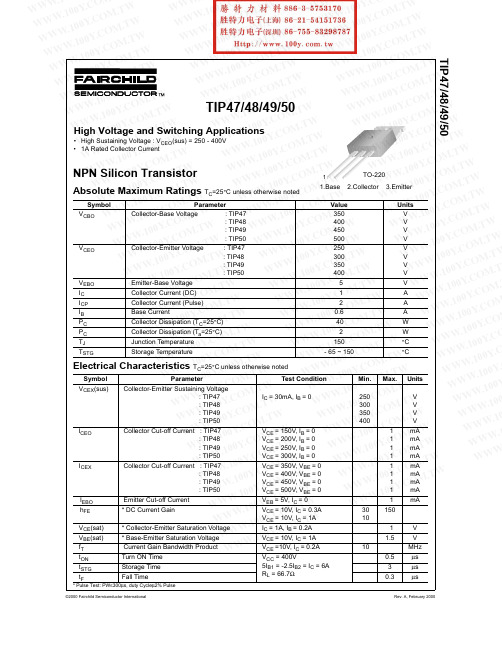
©2000 Fairchild Semiconductor InternationalRev. A, February 2000TIP47/48/49/50W W W .1W W W .100Y .C O M W W W .100Y .C O M .T W W W W .100Y .C O M .T W W W W .W .C O M .T W W W W .100Y .C O W W W .100Y .C O M .T W W W .100Y .C O M .T W W W W Y .C O M .T W W W W .100Y .C O W W W W .100Y .C O M .T W W W W .100Y .C O M .T W 0Y .C O M .T W T W W T W .T W M .T W M .T W O M .T W C O M .T W .C O M .T W Y .C O M .T W 0Y .C O M .T W 00Y .C O M .T W .100Y .C O M .T W .100Y .C O M .T W .100Y .C O M .W .100Y .C O M W W .100Y .C O M W W W .100Y .C O W W W .100Y .C W W W .100Y . W W W .100Y W W W .100 W W W .10 W W W .1 W W W©2000 Fairchild Semiconductor International TIP47/48/49/50Rev. A, February 2000W W W .1W W W .100Y .C O M W W W .100Y .C O M .T W W W W .100Y .C O M .T W W W W .W .C O M .T W W W W .100Y .C O W W W .100Y .C O M .T W W W .100Y .C O M .T W W W W Y .C O M .T W W W W .100Y .C O 0Y .C O M .T W W W W .100Y .C O M .T W M .T W W W W .100Y .C O M .T W W W W .100Y .C O M .T W W .100Y .T W W T W .T W M .T W M .T W O M .T W C O M .T W .C O M .T W Y .C O M .T W 0Y .C O M .T W 00Y .C O M .T W .100Y .C O M .T W .100Y .C O M .T W .100Y .C O M .W .100Y .C O M W W .100Y .C O M W W W .100Y .C O W W W .100Y .C W W W .100Y . W W W .100Y W W W .100 W W W .10 W W W .1 W W W©2000 Fairchild Semiconductor InternationalRev. A, February 2000TIP47/48/49/50W W W .1W W W .100Y .C O M W W W .100Y .C O M .T W W W W .100Y .C O M .T W W W W .W .C O M .T W W W W .100Y .C O W W W .100Y .C O M .T W W W .100Y .C O M .T W W W W W .100Y .C O M .T W W W W .100Y .C O W .100Y .C O M .T W W W W .100Y .C O M .T W W W .100Y .C O M .T W W W W .100Y .C O M .T W Y .C O M .T W W W W .10Y .C O M .T W W W W W .T W W W W W T W .T W M .T W M .T W O M .T W C O M .T W .C O M .T W Y .C O M .T W 0Y .C O M .T W 00Y .C O M .T W .100Y .C O M .T W .100Y .C O M .T W .100Y .C O M .W .100Y .C O M W W .100Y .C O M W W W .100Y .C O W W W .100Y .C W W W .100Y . W W W .100Y W W W .100 W W W .10 W W W .1 W W W©2000 Fairchild Semiconductor International Rev. ETRADEMARKS The following are registered and unregistered trademarks Fairchild Semiconductor owns or is authorized to use and is not intended to be an exhaustive list of all such trademarks.ACEx™Bottomless™CoolFET™CROSSVOLT™E 2CMOS™FACT™FACT Quiet Series™FAST ®FASTr™GTO™HiSeC™ISOPLANAR™MICROWIRE™POP™PowerTrench ®QFET™QS™Quiet Series™SuperSOT™-3SuperSOT™-6SuperSOT™-8SyncFET™TinyLogic™UHC™VCX™DISCLAIMER FAIRCHILD SEMICONDUCTOR RESERVES THE RIGHT TO MAKE CHANGES WITHOUT FURTHER NOTICE TO ANY PRODUCTS HEREIN TO IMPROVE RELIABILITY, FUNCTION OR DESIGN. FAIRCHILD DOES NOT ASSUME ANY LIABILITY ARISING OUT OF THE APPLICATION OR USE OF ANY PRODUCT OR CIRCUIT DESCRIBED HEREIN;NEITHER DOES IT CONVEY ANY LICENSE UNDER ITS PATENT RIGHTS, NOR THE RIGHTS OF OTHERS.LIFE SUPPORT POLICY FAIRCHILD’S PRODUCTS ARE NOT AUTHORIZED FOR USE AS CRITICAL COMPONENTS IN LIFE SUPPORT DEVICES OR SYSTEMS WITHOUT THE EXPRESS WRITTEN APPROVAL OF FAIRCHILD SEMICONDUCTOR INTERNATIONAL.As used herein:1. Life support devices or systems are devices or systems which, (a) are intended for surgical implant into the body,or (b) support or sustain life, or (c) whose failure to perform when properly used in accordance with instructions for use provided in the labeling, can be reasonably expected to result in significant injury to the user. 2. A critical component is any component of a life support device or system whose failure to perform can be reasonably expected to cause the failure of the life support device or system, or to affect its safety or effectiveness.PRODUCT STATUS DEFINITIONS Definition of Terms Datasheet Identification Product Status Definition Advance Information Formative or In Design This datasheet contains the design specifications for product development. Specifications may change in any manner without notice.Preliminary First Production This datasheet contains preliminary data, and supplementary data will be published at a later date.Fairchild Semiconductor reserves the right to make changes at any time without notice in order to improve design.No Identification Needed Full Production This datasheet contains final specifications. Fairchild Semiconductor reserves the right to make changes atany time without notice in order to improve design.Obsolete Not In ProductionThis datasheet contains specifications on a product that has been discontinued by Fairchild semiconductor.The datasheet is printed for reference information only.W W W .1W W W .100Y .C O M W W W .100Y .C O M .T W W W W .100Y .C O M .T W W W W .W W W .100Y .C O M .T W W W W .100Y .C O W W W .100Y .C O M .T W W W W .100Y .C O M .T W W W W .100Y .C O M .T W W W W .100Y .C O M .T W W W W W W W .100Y .C O M .T W W W W .100Y .C O M .T W W W W .100Y .C O W W W .100Y .C O M .T W W W W .100Y .C O M .T W W W W .100Y .C O M .T W W W W .100Y .C O M .T W W W W .100Y .C O M .T W W W W .100Y .C O M .T W W W W .100Y .C O M .T W W W W .100Y .C O M .T W W W W .100Y .C O M .T W W W W .100Y .C O M .T W W W W .100Y .C O M .T W W W W .100Y .C O M .T W W W W .100Y .C O M .T W W W W .100Y .C O M .T W W W W .100Y .C O M .T W W W W .100Y .C O M .T W W W W .100Y .C O M .T W W W W .100Y .C O M .T W W W W .100Y .C O M .T W W W W .100Y .C O M .T W W W W .100Y .C O M .T W W W W .100Y .C O M .T W W W W .100Y .C O M .T W W W W .100Y .C O M .T W W W W .100Y .C O M .T W W W W .100Y .C O M .T W W W W .100Y .C O M .T W W W W .100Y .C O M .T W W W W .100Y .C O M .T W W W W .100Y .C O M .T W W W W .100Y .C O M .T W W W W .100Y .C O M .T W W W W .100Y .C O M .T W W W W .100Y .C O M .T W W W W .100Y .C O M .T W W W W .100Y .C O M .T W W W W .100Y .C O M .T W W W W .100Y .C O M .T W W W W .100Y .C O M .T W W W W .100Y .C O M .T W W W W .100Y .C O M .T W W W W .100Y .C O M .T W W W W .100Y .C O M .T W W W W .100Y .C O M .T W W W W .100Y .C O M .T W W W W .100Y .C O M .T W W W W .100Y .C O M .T W W W W .100Y .C O M .T W W W W .100Y .C O M .T W W W W .100Y .C O M .T W W W W .100Y .C O M .T W W W W .100Y .C O M .T W W W W .100Y .C O M .T W W W W .100Y .C O M .T W W W W .100Y .C O M .T W W W W .100Y .C O M .T W W W W .100Y .C O M .T W W W .100Y .C O M .T W W W W .100Y .C O M .T W W W W .100Y .C O M .W W W .100Y .C O M .T W W W W .100Y .C O M .T W W W W .100Y .C O M W W W .100Y .C O M .T W W W W .100Y .C O M .T W W W W .100Y .C O M W W W .100Y .C O M .T W W W W .100Y .C O M .T W W W W .100Y .C O W W W .100Y .C O M .T W W W W .100Y .C O M .T W W W W .100Y .C W W W .100Y .C O M .T W W W W .100Y .C O M .T W W W W .100Y .W W W .100Y .C O M .T W W W W .100Y .C O M .T W W W W .100Y W W W .100Y .C O M .T W W W W .100Y .C O M .T W W W W .100W W W .100Y .C O M .T W W W W .100Y .C O M .T W W W W .10W W W .100Y .C O M .T W W W W .100Y .C O M .T W W W W .1W W W.100Y .C O M .T WW W W .100Y .C O M .T W W W W。
LCA127_DataSheet_Sige pole optoMOS Relay
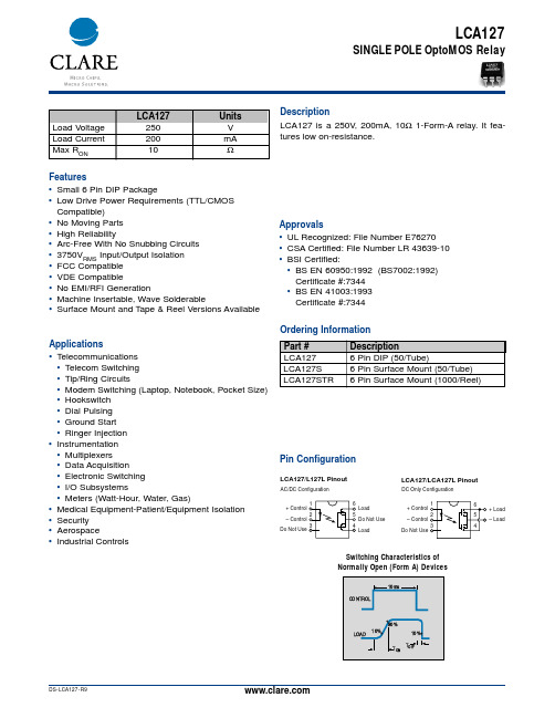
LCA127ApplicationsFeaturesDescriptionApprovalsOrdering InformationPin ConfigurationLCA127 is a 250V, 200mA, 10Ω1-Form-A relay. It fea-tures low on-resistance.•Telecommunications •Telecom Switching •Tip/Ring Circuits•Modem Switching (Laptop, Notebook, Pocket Size)•Hookswitch •Dial Pulsing •Ground Start •Ringer Injection •Instrumentation •Multiplexers •Data Acquisition •Electronic Switching •I/O Subsystems•Meters (Watt-Hour, Water, Gas)•Medical Equipment-Patient/Equipment Isolation •Security •Aerospace•Industrial Controls•UL Recognized: File Number E76270•CSA Certified: File Number LR 43639-10•BSI Certified:•BS EN 60950:1992 (BS7002:1992)Certificate #:7344 •BS EN 41003:1993Certificate #:7344•Small 6 Pin DIP Package•Low Drive Power Requirements (TTL/CMOS Compatible)•No Moving Parts •High Reliability•Arc-Free With No Snubbing Circuits •3750V RMS Input/Output Isolation •FCC Compatible •VDE Compatible•No EMI/RFI Generation•Machine Insertable, Wave Solderable•Surface Mount and Tape & Reel Versions Available+ Control – Control Do Not UseLoad Do Not Use LoadAC/DC ConfigurationLCA127/L127L Pinout–+ Load – LoadDC Only ConfigurationLCA127/LCA127L PinoutSwitching Characteristics of Normally Open (Form A) DevicesLCA127Absolute Maximum Ratings (@ 25o C)Absolute Maximum Ratings are stress ratings. Functional Array operation of the device at these or any other conditionsbeyond those indicated in the operational sections of thisdata sheet is not implied. Exposure of the device to theabsolute maximum ratings for an extended period maydegrade the device and effect its reliability.2Derate Linearly 6.67 mw/o CElectrical CharacteristicsLCA127Performance Data*The Performance data shown in the graphs above is typical of device performance. For guaranteed parameters not indicated in the written specifications, please contact our application department.LCA127Performance Data*The Performance data shown in the graphs above is typical of device performance. For guaranteed parameters not indicated in the written specifications, please contact our application department.LCA127Mechanical DimensionsDimensionsmm (inches)CLARE LOCATIONSClare Headquarters78 Cherry Hill DriveBeverly, MA01915Tel: 1-978-524-6700Fax: 1-978-524-4900Toll Free: 1-800-27-CLARE Clare Micronix Division145 ColumbiaAliso Viejo, CA92656-1490 Tel: 1-949-831-4622Fax: 1-949-831-4628SALES OFFICES AMERICASAmericas HeadquartersClare78 Cherry Hill DriveBeverly, MA01915Tel: 1-978-524-6700Fax: 1-978-524-4900Toll Free: 1-800-27-CLARE Eastern RegionClareP.O. Box 856Mahwah, NJ 07430Tel: 1-201-236-0101Fax: 1-201-236-8685Toll Free: 1-800-27-CLARE Central RegionClare Canada Ltd.3425 Harvester Road, Suite 202 Burlington, Ontario L7N 3N1 Tel: 1-905-333-9066Fax: 1-905-333-1824Western RegionClare1852 West 11th Street, #348 Tracy, CA95376Tel: 1-209-832-4367Fax: 1-209-832-4732Toll Free: 1-800-27-CLARE CanadaClare Canada Ltd.3425 Harvester Road, Suite 202 Burlington, Ontario L7N 3N1 Tel: 1-905-333-9066Fax: 1-905-333-1824EUROPEEuropean HeadquartersCP Clare nvBampslaan 17B-3500 Hasselt (Belgium)Tel: 32-11-300868Fax: 32-11-300890FranceClare France SalesLead Rep99 route de Versailles91160 ChamplanFranceTel: 33 1 69 79 93 50Fax: 33 1 69 79 93 59GermanyClare Germany SalesActiveComp Electronic GmbHMitterstrasse 1285077 ManchingGermanyTel: 49 8459 3214 10Fax: 49 8459 3214 29ItalyC.L.A.R.E.s.a.s.Via C. Colombo 10/AI-20066 Melzo (Milano)Tel: 39-02-95737160Fax: 39-02-95738829SwedenClare SalesComptronic ABBox 167S-16329 SpångaTel: 46-862-10370Fax: 46-862-10371United KingdomClare UK SalesMarco Polo HouseCook WayBindon RoadTauntonUK-Somerset TA2 6BGTel: 44-1-823 352541Fax: 44-1-823 352797ASIA PACIFICAsian HeadquartersClareRoom N1016, Chia-Hsin, Bldg II,10F, No. 96, Sec. 2Chung Shan North RoadTaipei, Taiwan R.O.C.Tel: 886-2-2523-6368Fax: 886-2-2523-6369Worldwide Sales OfficesSpecification: DS-LCA127-R9©Copyright 2001, Clare, Inc.All rights reserved. Printed in USA.02/02/01Clare cannot assume responsibility for use of any circuitry otherthan circuitry entirely embodied in this Clare product. No circuitpatent licenses nor indemnity are expressed or implied. Clarereserves the right to change the specification and circuitry, with-out notice at any time. The products described in this documentare not intended for use in medical implantation or other direct lifesupport applications where malfunction may result in direct phys-ical harm, injury or death to a person.。
- 1、下载文档前请自行甄别文档内容的完整性,平台不提供额外的编辑、内容补充、找答案等附加服务。
- 2、"仅部分预览"的文档,不可在线预览部分如存在完整性等问题,可反馈申请退款(可完整预览的文档不适用该条件!)。
- 3、如文档侵犯您的权益,请联系客服反馈,我们会尽快为您处理(人工客服工作时间:9:00-18:30)。
TIP120/121/122TIP125/126/127
COMPLEMENTARY SILICON POWER
DARLINGTON TRANSISTORS
s
STMicroelectronics PREFERRED SALESTYPES
DESCRIPTION The TIP120, TIP121 and TIP122 are silicon Epitaxial-Base NPN power transistors in monolithic Darlington configuration mounted in Jedec TO-220 plastic package. They are intented for use in power linear and switching applications.The complementary PNP types are TIP125,TIP126 and TIP127, respectively.
March 2000 ABSOLUTE MAXIMUM RATINGS
1/4
THERMAL DATA
ELECTRICAL CHARACTERISTICS (T case = 25 o
C unless otherwise specified)
For PNP types voltage and current values are negative.
TIP120/TIP121/TIP122/TIP125/TIP126/TIP127
TIP120/TIP121/TIP122/TIP125/TIP126/TIP127
Information furnished is believed to be accurate and reliable. However, STMicroelectronics assumes no responsibility for the consequences of use of such information nor for any infringement of patents or other rights of third parties which may result from its use. No license is granted by implication or otherwise under any patent or patent rights of STMicroelectronics. Specification mentioned in this publication are subject to change without notice. This publication supersedes and replaces all information previously supplied. STMicroelectronics products are not authorized for use as critical components in life support devices or systems without express written approval of STMicroelectronics.
The ST logo is a trademark of STMicroelectronics
© 2000 STMicroelectronics – Printed in Italy – All Rights Reserved
STMicroelectronics GROUP OF COMPANIES
Australia - Brazil - China - Finland - France - Germany - Hong Kong - India - Italy - Japan - Malaysia - Malta - Morocco - Singapore - Spain - Sweden - Switzerland - United Kingdom - U.S.A.
TIP120/TIP121/TIP122/TIP125/TIP126/TIP127。