Mouser供货TI TUSB320 CC 逻辑和端口控制器
星光莱特 LT-320触摸式控制屏操作说明说明书

本文档只针对北京星光莱特电子有限公司生产的LT-320新型触摸式控制屏做操作说明,部分相关设置使用附带的LC灯光控制软件。
LC详细操作请参软件相关使用说明。
LT-320触摸式控制屏使用说明北京星光莱特电子有限公司BEIJING STARLIGHT ELECTRONICS CO.,LTD北京市大兴区西红门镇星光巷7号100076新的LT-320触摸式控制屏基于LC软件编程,通过PC软件实现电脑对终端设备和触摸屏的设置。
对终端设备的设置包括:地址设置,区域设置,亮度设置,场景保存和场景检查。
对触摸屏的设置包括:按键设置,定时设置,天文时间。
使用LC控制软件将更加快捷方便的赋予触摸屏更加强大的功能。
一.接线示意图:(接线之前,先给USB-RS-485安装驱动程序,见光盘)接通电源,进入初始画面如下:二.点击屏幕左下角的“LIGHTSPACE”,进入输入密码画面,输入正确密码(默认为1665)后,按“确定”后,进入“主菜单”画面。
1.联机设置点击“联机设置”菜单,液晶屏显示如下界面,只有在此界面下方可使用LC软件对触摸屏进行有效编程。
点击“返回”回到上级菜单。
2.设置语言点击“设置语言”菜单,触摸屏提供中英文两种语言选择,点击选中任一种语言,该语种背景反白,则设置成功。
点击“返回”键回到上级菜单。
3.初始化设置点击“初始化设置”菜单,触摸屏界面如下,初始化设置将使触摸屏当前的一切设置丢失,返回到出厂状态,请慎重操作。
点击“返回”键回到上级菜单。
4.更新时间点击“更新时间”菜单,触摸上下箭头更改年,月,日,星期及时间值,按“确定”键确认更改。
点击“返回”键回到上级菜单。
5.修改密码点击“修改密码”菜单,进入修改密码菜单,按照提示设定四位新密码,设置好后点击“确定”键。
放弃修改请点击“取消”。
点击“返回”键回到上级菜单。
6.液晶亮度点击“液晶亮度”菜单,进入液晶亮度设置菜单,点击上下箭头改变亮度。
点击“返回”键回到上级菜单。
速度特克320CP推挽类产品零件电路图说明书

IM307511/2020REV05SPEEDTEC 320CPSPEEDTEC 320CP Push PullSpare Parts (1)Figure A. Casing (2)Figure B. Wire Feeding (3)Figure C. Internal Parts (4)Figure D. Front Assembly (5)Figure E. Inverter (6)Figure F. Back assembly (7)Electrical Schematic (8)CODE: 50393 (8)CODE: 50501 (9)Lincoln Electric Bester Sp. z o.o.ul. Jana III Sobieskiego 19A, 58-260 Bielawa, Polandwww.lincolnelectric.euSpare Parts50393 REV0111/18ASSEMBLY PAGE NAMEC a s i n gW i r e F e e d i n gI n t e r n a l P a r t sW i r e D r i v e F r o n t A s s e m b l yn v e r t e rB a c k A s s e m b l y E l e c t r i c a lD i a g r a m CODE NO.: W NO.: FIGURE NO.: A B C C EFG50393 K14168-1 SPEEDTEC 320 CP 1 1 1 1 1 1 1 50501 K14168-2 SPEEDTEC 320 CP/PP 1 1 1 1 1 1 1Figure AFigure A. CasingItem Description Part Number Qty 1 2 3 4 5 6 7 01 BOTTOMASSEMBLY R-3019-497-1R 1 X X02 COVERASSEMBLY R-3019-498-1R 1 X X03 LATERAL PANEL ASSEMBLY R-1019-545-1R 1 X X04 LOCKINGUNITHINGE W000278021 2 X X05 ASA SPEEDTEC 400S/500S(HANDLE) R-0010-292-1R 2 X X06 CORNERCAP W95x1147R 4 X X07 LOQUETCOULISSANTAFFLEURANT W000241671 2 X X08 DOORINKED R-1019-544-1R 1 X X09 TORCH HOLDER (COMPLET AVEC87000055P)W000402488 1 X X10 STICKER 3YEARS WARRINTY D-2837-731-2 2719-107-823R 1 X X11 STICKERLIFTING R-0010-332-1R 1 X X 12 STICKERWARNINGSD-2837-728-1 2719-107-728R 1 X XFigure BFigure B. Wire FeedingItem Description Part Number Qty 1 2 3 4 5 6 713 PLASTIC SPOOL AXIS DV44J W000149075 1 X X14 4 ROLLS COD150PDVU DMU P400 W000277988 1 X XSWITCH W000147188 1 X X15 SWITCH2PB300 W000385691 1 X X16 ADAPTERFigure CFigure C. Internal PartsItem Description Part Number Qty 1 2 3 4 5 6 7 17 FERRITEFLAT W000376585 2 X XTURNS 90002919PR 1 X X818 CHOKE19 POWERTRANSFORMER W000385778 1 X X20 RIBBON CABLES PULS III W000384735 1 X XCOMMAND W000386035 1 X XCYCLE21 PCBSUPPLY W000277882 1 X XAUXILAIRY22 PCB23 ENCODERBOARD W000386042 1 X X35-50MM W000010560R 1 X X24 MALECONNECTORBOARD E523-01R 1 XPULL54 PUSHFigure DFigure D. Front AssemblyItem Description Part Number Qty 1 2 3 4 5 6 7 ASSEMBLY R-3019-492-1R 1 X XPANEL25 FRONTPANEL 91633329PR 1 X X26 BOARDFRONT27 FRONT PANEL BOARD SUPPORT R-3019-493-1 1 X X28 FRONT NAMEPLATE SPEEDTEC 320 CP R-0010-725-1R 2 X XINCHES 9SM22778-1 2 X X29 KNOB1INCHES 9SM22778-2 4 X X1.530 KNOB31 PRESA FEMMINIA SALD.OPTIP 500I W000148911 2 X X320C R-5241-033-1R 1 X32 “J”HARNESSES32A J” HARNESSES 320C PUSH PULL R-5041-600-1R 1 XCLAMP 04081581PR 1 X X33 CABLE34 LEM 90000389PR 1 X XPLATE 90002713PR 1 X X35 STICKERBOARD W000386043 1 X XFILTER36 SECONDARYEMC37 PLASTIC INSULATOR EURO CONNECTOR 90003007PR 1 X XFigure EFigure E. InverterItem Description Part Number Qty 1 2 3 4 5 6 7 38 PCBPRIMARY W000386030 1 X X39 PCB SECONDARY WITH LED W000386031 1 X X40 BRIDGERECTIFIER W000386032 1 X X41 CURRENTSENSETRANSFORMER 90002925PR 1 X X42 GENERICTHERMALSENSOR 90002863PR 1 X X43 FAN EQUIP DGPIII COMPACT WORKINGSKETCHR-5241-002-1R 1 X XFigure FFigure F. Back assemblyItem Description Part Number Qty 1 2 3 4 5 6 7 44 BACKASSEMBLY R-3019-494-1R 1 X X45 PLASTICFRAMEREAR W000373702 1 X X46 SOLENOID VALVE 24V DC DIGIPULS II W000278017 1 X X47 PRIMARY FILTER BOARD NCI WORKINGSKETCHR-5241-001-1R 2 X X48 TRANSFORMER 200VA III 320C W000386041 2 X X49 STICKERPLATEWIRE 90002486PR 4 X X 50 POWERCABLE R-5241-011-1R 2 X X 51 SWITCH40A W000385787 1 X X 52 FERRITETORE36X23X15 90002996PR 1 X X 53 COOLERHARNESS R-5241-079-1R 1 X XElectrical Schematic CODE: 50393CODE: 50501。
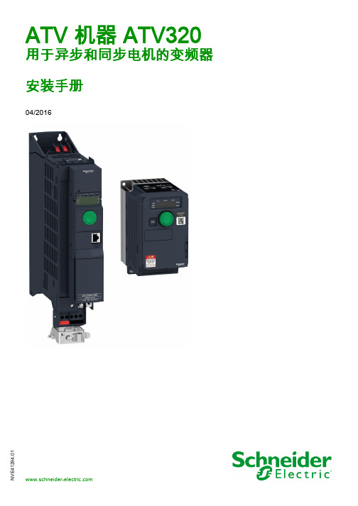
ATV320_安装手册_CN_NVE41294_01
60
电磁兼容性. . . . . . . . . . . . . . . . . . . . . . . . . . . . . . . . . . . . . . . . . . . . . . . . . . . . . . . . . . . . . . .
63
在 IT 或拐角接地系统上运行 . . . . . . . . . . . . . . . . . . . . . . . . . . . . . . . . . . . . . . . . . . . . . . . . .
40
线缆长度说明 . . . . . . . . . . . . . . . . . . . . . . . . . . . . . . . . . . . . . . . . . . . . . . . . . . . . . . . . . . . . .
42
接线图 . . . . . . . . . . . . . . . . . . . . . . . . . . . . . . . . . . . . . . . . . . . . . . . . . . . . . . . . . . . . . . . . . .
33
安装条件 . . . . . . . . . . . . . . . . . . . . . . . . . . . . . . . . . . . . . . . . . . . . . . . . . . . . . . . . . . . . . . . .
34
安装 . . . . . . . . . . . . . . . . . . . . . . . . . . . . . . . . . . . . . . . . . . . . . . . . . . . . . . . . . . . . . . . . . . . .
西门子自动化产品报价单

南京市珠江路185号 TEL:025-83222029 FAX:025-83603381
南京市珠江路185号 TEL:025-83222029 FAX:025-83603381
南京硕勋自动化工程有限公司
CP 340-1 TTY CP 340-1 RS485 CP 341-1 RS232 CP 341-1 TTY CP 341-1 RS485 CP 342-2 CP 342-5 CP 342-5 CP 343-1 经济型 CP 343-1 CP 343-1 CP 343-1 ISO CP 343-5 Profibus Cable RS 232 Cable 5M RS 20mA(TTY)Cable 5M RS 422/485Cable 5M MPI Cable 总线连接器 总线连接器 中继器 编程适配器 232 RS232 Cable 编程适配器 USB 总线连接器 6ES7 340-1BH02-0AE0 6ES7 340-1CH02-0AE0 6ES7 341-1AH01-0AE0 6ES7 341-1BH01-0AE0 6ES7 341-1CH01-0AE0 6GK7 342-2AH01-0XA0 6GK7 342-5DA02-0XA0 6GK7 342-5DF00-0XE0 6GK7 343-1CX00-0XE0 6GK7 343-1EX21-0XE0 6GK7 343-1GX20-0XE0 6GK7 343-1BA00-0XE0 6GK7 343-5FA01-0XE0 6XV1 830-0EH10 6ES7 902-1AB00-0AA0 6ES7 902-2AB00-0AA0 6ES7 902-3AB00-0AA0 6ES7 901-0BF00-0XA0 6ES7 972-0BA12-0XA0 6ES7 972-0BB12-0XA0 6ES7 972-0AA01-0XA0 6ES7 972-0CA23-0XA0 6ES7 901-1BF00-0XA0 6ES7 972-0CB20-0XA0 6ES7 972-0BA50-0XA0 4855.00 4855.00 7360.00 7910.00 7910.00 6190.00 6900.00 8600.00 6200.00 11700.00 16300.00 12700.00 8100.00 12.80 724.00 724.00 724.00 281.00 337.50 450.00 2756.00 3200.00 165.00 3060.00 337.50
320温度传感器系列温度 过程控制器说明书
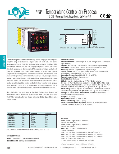
VISIT OUR WEBSITES: • • .auLatest microprocessor based technology affords full programmability with complete array o eatures in compact ultra low cost unit. 16A Series Temperature/Process Controller eatures universal input, Sel -Tune PID,Fuzzy Logic, and dual four-digit LED displays for process and set point value.Selectable inputs can be thermocouple, RTD, current or voltage. Available out-puts are solid-state relay, relay, pulsed voltage, or proportional current.Programmable alarm (optional) can be reset automatically or manually. Front panel is waterproof and corrosion resistant (UL type 4-X), making it ideal for sanitary applications. Replace electronics without wiring changes (via remov-able front panel). Self diagnostics, nonvolatile memory and selectable control modes are all designed for greater productivity. Four security levels are pass-word protected. On-of f , P, PI or PID manual tune control f unctions can be selected or the controller will Self-Tune automatically for best PID control.The 16A2 o ers the best value in Standard Features in a Process and Temperature control. In addition to the features listed above, the 16A2 offers Peak/Valley indication, Percent Output indication, Digital Input Filter, and a host of others.For Enhanced Ramp and Soak features, change 16A2 to 16A3Temperature Controller/Process1/16 DIN, Universal lnput, Fuzzy Logic, Self-TunePIDSeries 16A** These options may not be combined with each other.SPECIFICATIONSSelectable Inputs:Thermocouple, RTD, DC Voltage, or DC Current (See Input Ranges).Display:Two four-digit LED displays, 0.3 in (7.62 mm) high. Display Resolution: 1 degree or 0.1 degree (sensor dependent), or 1 count.Accuracy:±0.25% of span ±1 least significant digit.Supply Voltage: 100 to 240 VAC nominal, +10% -15%, 50 to 400 Hz single phase; 132 to 240 VDC +10% -20%.Operating Temperature: 14 to 131°F (-10 to 55°C).Power Consumption: 5 VA maximum.Control Output Ratings:SSR: 2.0 A at 240 VAC resistive at 77°F (25°C). De-rates to1.0 A at 130°F (55°C). Minimum load of 100 mA. DC SSR:1.75 A at 32VDC maximum.Relay: SPST, 3A at 240 VAC resistive, 1.5 A @ 240 VAC inductive. Pilot Duty rating: 250 VA, 2 A @ 120 VAC, 1 A @ 240 VAC.Alarm Relay: SPST, 3 A @ 240 VAC resistive; 1.5 A @ 240 VAC inductive.Pilot Duty Rating: 240 VA, 2 A @ 120 VAC or 1 A @ 240 VAC. Switched Voltage: 15 VDC at 20 mA. Proportional Current: 0 to 20 mADC,scalable, into 600 ohms maximum.Weight: 8 oz (227g).Agency Approvals: UL E83725, CE.Front Panel Rating: Type 4X (IP66).Serial Communications (Optional): RS-232 or RS-485 with either LoveLink ™Software or Modbus ®RTU protocol.Modbus ®is a registered trademark of Schnieder Automation .ACCESSORIESOPTIONS934**, Process Signal Output, PV or SV . Isolated 0 to 20 mADC936**, Process Signal Output, PV or SV . Isolated 0 to 10 VDC992**,RS-XXX Serial Communications Lovelink TM Protocol993**,RS-XXX Serial Communications Lovelink TM Protocol 995**, RS-XXX Serial Communications Modbus RTV Protocol 996**, RS-XXX Serial Communications Modbus RTV Protocol 9502, 12-24 VDC/VAC power inputMN-1,Mini-Node ™USB/RS-485 converter LoveLinks III,Configuration software。
施耐德PL7软件手册

0
TSX 37-05/08/10/21/22 PLCs
用于简单 I/O 连接个数 Preventa 安全模块 远程 I/O Telefast 2 实时时钟 模拟量 I/O
过程控制 计数、定位
通讯
软件结构 内存结构 供电电压 标准 I/O
PLC 类型 页数 1/2
本体单元 扩展接口 每个 HE 10 连接器 每个端子块
b TSX 37 21/22PLC . . . . . . . . . . . . . . . . . . . . . . . . . . . . . . . . . . . . . . . . . . . . . . 1/7
b 功能、内存结构 . . . . . . . . . . . . . . . . . . . . . . . . . . . . . . . . . . . . . . . . . . . . . . . . . 1/8
–
60
88
124
紧急停机,以及对极限开关进行监控
96 个远程 I/O (4 个 Nano PLC) c 24 V 输入, a 115 V 输入
8、 12 或 16 通道,带或不带 LED,每个通道带 1 个或 2 个端子
8 或 16 通道,c 5 V TTL, c 24 V, c 48 V, a 115 或 230 V,每通道带 2 个端子 集成 ( 分、秒 )
@ 请参考相关产品样本
Schneider Electric
1
1
1/0
Schneider Electric
目录
1 - Modicon TSX Micro
0
自动化平台
1 - Modicon TSX Micro PLC
NJ400 可编程控制器(PLC)硬件手册说明书

基本说明✧感谢您购买了傲拓科技股份有限公司(简称傲拓科技)系列可编程序控制器。
✧在使用产品之前,请仔细阅读本手册,并在充分理解手册内容的前提下,进行使用。
✧软件及编程方面的介绍,请查阅相关手册。
✧请将本手册交付给最终用户。
用户须知✧使用产品要求在控制系统的设计和编程方面有经验。
只允许具有此类经验的人士编程、安装、改动和应用此产品。
电气设备的安装、操作、维修和维护工作仅限于合格人员执行。
✧手册等其他技术资料中所列举的示例仅供用户理解、参考用,不保证一定动作。
✧将该产品与其他产品组合使用的时候,请确认是否符合相关规定、原则、技术要求等。
✧使用该产品时,请自行确认是否符合要求以及安全,对于本产品故障而可能引发机器故障或损失时,请自行设置后备及安全功能。
不遵守本产品的相关警告可能导致人身伤害或设备损坏。
✧在安装和使用本产品时,必须遵守国家/地区、区域和当地的所有相关的安全法规。
出于安全方面的考虑和为了确保符合归档的系统数据,只允许制造商对各个组件进行维修。
✧对于使用本资料所引发的任何后果,傲拓科技概不负责。
✧我们已核对本手册中的内容、图表与所述硬件设备相符,但误差难以避免,并不能保证完全一致。
我们会定期对手册的内容进行检查、修改和维护,恕不另行通知。
版权申明✧本手册内容,包括文字、图表、标志、标识、商标、产品型号、软件程序、版面设计等,均受《中华人民共和国著作权法》、《中华人民共和国商标法》、《中华人民共和国专利法》及与之适用的国际公约中有关著作权、商标权、专利权或其他财产所有权法律的保护,为傲拓科技专属所有或持有。
✧未经傲拓科技明确书面许可,不得以任何形式、通过任何电子或机械手段(包括复印)复制本文档的任何部分。
✧傲拓科技保留全部权利。
✧手册中涉及到的其他商标或注册商标属于他们各自的拥有者。
联系方式如果您有任何关于本产品的使用问题,请与购买产品的代理商、办事处联系,也可以直接与傲拓科技联系。
✧电话:************✧传真:************✧网址:https://✧地址:江苏省南京市雨花台区云密城D栋8层目录前言 (1)第一章硬件系统概述 (3)1.1NJ400硬件系统组成及结构 (4)1.2NJ400技术特色 (4)1.3NJ400系统指标 (5)1.4产品清单 (6)1.5NJ400硬件系统配置 (9)第二章 CPU模块 (15)2.1标准单网CPU401-0211 (17)2.2高性能双网CPU401-0411 (22)2.3高性能冗余CPU401-0511 (27)2.4高性能双网CPU401-0441 (32)2.5高性能冗余CPU401-0541 (39)第三章电源模块 (45)3.1电源模块PWM401-0501 (46)3.2电源模块PWM401-0801 (49)3.3电源模块PWM401-1001 (52)3.4电源模块PWM401-0502 (55)3.5电源模块PWM401-0802 (58)3.6电源模块PWM401-1002 (61)3.7冗余电源模块24V-DC输入 (64)第四章数字量模块 (68)4.1数字量输入模块DIM401-1601:DI16×DC24V (70)4.2数字量输入模块DIM401-1601CT:DI16×DC24V (74)4.3数字量输入模块DIM401-1602:DI16×DC24V (77)4.4数字量输入模块DIM401-1602CT:DI16×DC24V (80)4.5数字量输入模块DIM401-3201:DI32×DC24V (84)4.6数字量输入模块DIM401-3201CT:DI32×DC24V (88)4.7数字量输入模块DIM401-3202:DI32×DC24V (93)4.8数字量输入模块DIM401-3202CT:DI32×DC24V (97)4.9事件记录模块IIM401-1601:IIM16×DC24V (102)4.10事件记录模块IIM401-1601CT:IIM16×DC24V (107)4.11事件记录模块IIM401-3201:IIM32×DC24V (111)4.12事件记录模块IIM401-3201CT:IIM32×DC24V (116)4.13数字量输出模块DOM401-1601:DO16×DC24V×晶体管 (121)4.14数字量输出模块DOM401-1601CT:DO16×DC24V×晶体管 (125)4.15数字量输出模块DOM401-1602:DO16×继电器 (128)4.16数字量输出模块DOM401-1602CT:DO16×继电器 (132)4.17数字量输出模块DOM401-3201:DO32×DC24V×晶体管 (135)4.18数字量输出模块DOM401-3201CT:DO32×DC24V×晶体管 (139)第五章模拟量模块 (144)5.1模拟量输入模块AIM401-0801:AI8×电流 (146)5.2模拟量输入模块AIM401-0801CT:AI8×电流 (150)5.3模拟量输入模块AIM401-1601:AI16×电流 (153)5.4模拟量输入模块AIM401-1601CT:AI16×电流 (156)5.5模拟量输入模块AIM401-0802:AI8×电流电压混合型 (160)5.6模拟量输入模块AIM401-0802CT:AI8×电流电压混合型 (164)5.7模拟量输入模块AIM401-0803:AI8×电压 (167)5.8模拟量输入模块AIM401-0803CT:AI8×电压 (171)5.9模拟量输入模块AIM401-1603:AI16×电压 (174)5.10模拟量输入模块AIM401-1603CT:AI16×电压 (178)5.11模拟量输入模块AIM401-0404:AI4×电流电压混合型 (181)5.12模拟量输入模块AIM401-0404CT:AI4×电流电压混合型 (185)5.13模拟量输入模块AIM401-0804:AI8×电流电压混合型 (188)5.14模拟量输入模块AIM401-0804CT:AI8×电流电压混合型 (192)5.15模拟量输入模块AIM401-0805:AI8×RTD (195)5.16模拟量输入模块AIM401-0805CT:AI8×RTD (199)5.17模拟量输入模块AIM401-0806:AI8×热电偶 (203)5.18模拟量输入模块AIM401-0806CT:AI8×热电偶 (208)5.19模拟量输出模块AOM401-0401:AO4×电流 (212)5.20模拟量输出模块AOM401-0401CT:AO4×电流 (216)5.21模拟量输出模块AOM401-0402:AO4×电流/电压混合型 (219)5.22模拟量输出模块AOM401-0402CT:AO4×电流/电压混合型 (224)5.23模拟量输出模AOM401-0802:AO8×电流/电压混合型 (228)5.24模拟量输出模块AOM401-0802CT:AO8×电流/电压混合型 (232)第六章功能模块 (237)6.1高速计数模块HCM401-0801 (238)6.2高速计数模块HCM401-0302 (253)6.3高速输出模块HOM401-0801 (262)第七章通讯模块 (269)7.1串口通讯模块CMM401-0411 (270)7.2CANO PEN 主站模块CMM401-0104 (274)7.3D EVICE N ET 主站模块CMM401-0106 (277)7.4以太网远程IO主站模块CMM401-0108 (282)7.5以太网远程IO子站模块CMM401-0118 (288)7.6以太网远程IO子站模块CMM401-0118_SFP (294)7.7通讯模块(以太网):CMM401-0205 (301)7.8自定义CAN模块CMM401-0114 (305)第八章系统配置 (310)8.1I/O模块的选择 (310)8.2CPU的选择 (311)8.3模块安装底板的选择 (312)8.4系统配置案例 (315)第九章硬件安装 (318)9.1模块底板的安装 (318)9.2模块的安装 (319)9.3预接线电缆CNL401-0255T(V2.0) (322)9.4通信模件扩展电缆CNL401-0203(V1.0) (323)9.5配线要求 (324)第十章配件和附件 (326)前言NJ系列可编程控制器(简称NJ-PLC)由傲拓科技股份有限公司自主设计与研发,汲取了国际主流PLC的成功经验,改进了其不足之处,瞄准了当今PLC的最新发展方向,采用了计算机、通信、电子和自动控制等方面的国际先进技术,在CPU操作系统、I/O信号处理、网络通讯、软件开发及生产工艺等方面具有优越的性能,是适用于各种自动化控制的可编程控制器。
阿特美 AT97SC3204 信任平台模块数据手册摘要说明书
This is a summary document. The complete document is available under NDA. For more information, please contact your local Atmel sales office. Features●Fully compliant to the Trusted Computing Group (TCG) Trusted Platform Module(TPM) version 1.2 specification●Compliant with TCG PC client-specific TPM Interface Specification (TIS) version 1.2●Single-chip, turnkey solution●Hardware asymmetric crypto engine●Atmel® AVR® RISC microprocessor●Internal EEPROM storage for RSA keys●33MHz Low Pin Count (LPC) bus for easy PC interface●Secure hardware and firmware design and chip layout●Internal, high-quality Random Number Generator (RNG) – FIPS 140-2 compliant●NV storage space for 1756 bytes of user defined data● 3.3V supply voltage●28-lead thin TSSOP, 28-lead wide TSSOP, or 40-pad QFN packages●Offered in both commercial (0 to 70°C) and industrial (-40 to +85°C)temperature rangesDescriptionThe Atmel AT97SC3204 is a fully integrated security module designed to be integrated into personal computers and other embedded systems. It implements version 1.2 of the Trusted Computing Group (TCG) specification for Trusted Platform Modules (TPM).The TPM includes a cryptographic accelerator capable of computing a 2048-bit RSA signature in 200ms and a 1024-bit RSA signature in 40ms. Performance of the SHA-1 accelerator is 20μs per 64-byte block.The chip communicates with the PC through the LPC interface. The TPM supports SIRQ (for interrupts) and CLKRUN to permit clock stopping for power savings in mobile computers.Atmel AT97SC3204Trusted Platform Module LPC InterfaceSUMMARY DATASHEET1.Pin Configurations and PinoutsTable 1-1.Pin ConfigurationsTable 1-2.Pinouts2.Block DiagramThe TPM includes a hardware random number generator, including a FIPS-approved Pseudo Random NumberGenerator that is used for key generation and TCG protocol functions. The RNG is also available to the system togenerate random numbers that may be needed during normal operation.The chip uses a dynamic internal memory management scheme to store multiple RSA keys. Other than the standard TCG commands (TPM_FlushSpecific, TPM_Loadkey2), no system intervention is required to manage this internal key cache.The TPM is offered to OEM and ODM manufacturers as a turnkey solution, including the firmware integrated on the chip.In addition, Atmel provides the necessary device driver software for integration into certain operating systems, along with BIOS drivers. Atmel will also provide manufacturing support software for use by OEMs and ODMs during initialization and verification of the TPM during board assembly.Full documentation for TCG primitives can be found in the TCG TPM Main Specification, Parts 1 to 3, on the TCG Web site located at https://. TPM features specific to PC Client platforms are specified in the “TCG PC Client Specific TPM Interface Specification, Version 1.2”, also available on the TCG web site. Implementation guidance for 32-bit PC platforms is outlined in the “TCG PC Client Specific Implementation Specification for Conventional BIOS for TCG Version 1.2”, also available on the TCG website.3.Ordering InformationNote: 1.Please see the AT97SC3204 datasheet addendum for the complete catalog number ordering code.4.Package Drawings4.128X1 — 28-lead Thin TSSOP4.240ML1 — 40-pad VQFN5.Revision HistoryAtmel Corporation1600 Technology Drive, San Jose, CA 95110 USA T: (+1)(408) 441.0311F: (+1)(408) 436.4200| © 2013 Atmel Corporation. All rights reserved. / Rev.: Atmel-5295ES-TPM-AT97SC3204-LPC-Interface-Datasheet-Summary-032013Atmel®, Atmel logo and combinations thereof, Enabling Unlimited Possibilities®, AVR®, and others are registered trademarks or trademarks of Atmel Corporation or its subsidiaries. Other terms and product names may be trademarks of others.Disclaimer: The information in this document is provided in connection with Atmel products. No license, express or implied, by estoppel or otherwise, to any intellectual property right is granted by this document or in connection with the sale of Atmel products. EXCEPT AS SET FORTH IN THE ATMEL TERMS AND CONDITIONS OF SALES LOCATED ON THE ATMEL WEBSITE, ATMEL ASSUMES NO LIABILITY WHATSOEVER AND DISCLAIMS ANY EXPRESS, IMPLIED OR STATUTORY WARRANTY RELATING TO ITS PRODUCTS INCLUDING, BUT NOT LIMITED TO, THE IMPLIED WARRANTY OF MERCHANTABILITY, FITNESS FOR A PARTICULAR PURPOSE, OR NON-INFRINGEMENT. IN NO EVENT SHALL ATMEL BE LIABLE FOR ANY DIRECT, INDIRECT, CONSEQUENTIAL, PUNITIVE, SPECIAL OR INCIDENTAL DAMAGES (INCLUDING, WITHOUT LIMITATION, DAMAGES FOR LOSS AND PROFITS, BUSINESS INTERRUPTION, OR LOSS OF INFORMATION) ARISING OUT OF THE USE OR INABILITY TO USE THIS DOCUMENT, EVEN IF ATMEL HAS BEEN ADVISED OF THE POSSIBILITY OF SUCH DAMAGES. Atmel makes no representations or warranties with respect to the accuracy or completeness of the contents of this document and reserves the right to make changes to specifications and products descriptions at any time without notice. Atmel does not make any commitment to update the information contained herein. Unless specifically provided otherwise, Atmel products are not suitable for, and shall not be used in, automotive applications. Atmel products are not intended, authorized, or warranted。
施耐德 ATV320U07N4C 变频器 ATV320 数据表

Product data sheetCharacteristicsATV320U07N4C变频器 ATV320 - 0.75kW - 380…500V - 三项(紧凑型)主要信息产品系列ATV320产品类型变频器应用领域复杂机器变量标准版本驱动器格式紧凑型安装类型壁挂式安装通讯端口协议Modbus 串行CANopen选项卡通讯模块, CANopen 通讯模块, EtherCAT通讯模块, Profibus DP V1 通讯模块, Profinet通讯模块, 以太网Powerlink 通讯模块, Ethernet/IP 通讯模块, DeviceNet 额定电源电压 [Us]380...500 V - 15...10 %额定输出电流 2.3 A电动机功率 (kW)0.75 KW 适用 重载EMC 滤波器C2类EMC滤波器IP防护等级IP20补充信息离散量输入数量7数字量输入类型STO 安全扭矩中断, 24 V 直流, 阻抗: 1.5 kOhm DI1...DI6 逻辑输入, 24 V 直流 (30 V)DI5 可编程为脉冲输入: 0…30 kHz, 24 V 直流 (30 V)离散量输入逻辑正逻辑(源) 负逻辑 (漏)离散量输出数量3输出型式开放式集电器 DQ+ 0…1 kHz 30 V 直流 100 mA 开放式集电器 DQ- 0…1 kHz 30 V 直流 100 mA 模拟量输入数量3模拟量输入类型AI1 电压: 0...10 V 直流, 阻抗: 30 kOhm, 分辨率 10 位AI2 双极差分电压: +/- 10 V 直流, 阻抗: 30 kOhm, 分辨率 10 位AI3 电流: 0...20 mA (或 4-20 mA, x-20 mA, 20-x mA 或其他配置模式), 阻抗: 250 Ω, 分辨率 10 位模拟量输出数量1模拟量输出 型号软件-可配置电流 AQ1: 0...20 mA 阻抗 800 Ω, 分辨率 10 bits 软件-可配置电压 AQ1: 0...10 V 直流 阻抗 470 Ω, 分辨率 10 bitsT h e i n f o r m a t i o n p r o v i d e d i n t h i s d o c u m e n t a t i o n c o n t a i n s g e n e r a l d e s c r i p t i o n s a n d /o r t e c h n i c a l c h a r a c t e r i s t i c s o f t h e p e r f o r m a n c e o f t h e p r o d u c t s c o n t a i n e d h e r e i n .T h i s d o c u m e n t a t i o n i s n o t i n t e n d e d a s a s u b s t i t u t e f o r a n d i s n o t t o b e u s e d f o r d e t e r m i n i n g s u i t a b i l i t y o r r e l i a b i l i t y o f t h e s e p r o d u c t s f o r s p e c i f i c u s e r a p p l i c a t i o n s .I t i s t h e d u t y o f a n y s u c h u s e r o r i n t e g r a t o r t o p e r f o r m t h e a p p r o p r i a t e a n d c o m p l e t e r i s k a n a l y s i s , e v a l u a t i o n a n d t e s t i n g o f t h e p r o d u c t s w i t h r e s p e c t t o t h e r e l e v a n t s p e c i f i c a p p l i c a t i o n o r u s e t h e r e o f .N e i t h e r S c h n e i d e r E l e c t r i c I n d u s t r i e s S A S n o r a n y o f i t s a f f i l i a t e s o r s u b s i d i a r i e s s h a l l b e r e s p o n s i b l e o r l i a b l e f o r m i s u s e o f t h e i n f o r m a t i o n c o n t a i n e d h e r e i n .继电器输出类型可配置的继电器逻辑 R1A 1 NO 电气寿命 100000 次可配置的继电器逻辑 R1B 1NC 电气寿命 100000 次可配置的继电器逻辑 R1C可配置的继电器逻辑 R2A 1 NO 电气寿命 100000 次可配置的继电器逻辑 R2C最大开关电流继电器输出 R1A, R1B, R1C 在…上 阻性(负载) 量, cos phi = 1: 3 A 在…上 250 V AC继电器输出 R1A, R1B, R1C 在…上 阻性(负载) 量, cos phi = 1: 3 A 在…上 30 V 直流继电器输出 R1A, R1B, R1C, R2A, R2C 在…上 感性负载 量, cos phi = 0.4 L/R = 7 ms: 2 A 在…上继电器输出 R1A, R1B, R1C, R2A, R2C 在…上 感性负载 量, cos phi = 0.4 L/R = 7 ms: 2 A 在…上继电器输出 R2A, R2C 在…上 阻性(负载) 量, cos phi = 1: 5 A 在…上 250 V AC继电器输出 R2A, R2C 在…上 阻性(负载) 量, cos phi = 1: 5 A 在…上 30 V 直流最小开关电流 [Imin]继电器输出 R1A, R1B, R1C, R2A, R2C: 5 mA 在…上 24 V 直流访问方法从(站) CANopen4 quadrant operation possible True异步电机控制配置文件电压/频率比,5点无传感器磁链矢量控制标准电压/频率比无传感器磁链适量控制-节能电压/频率比,2点同步电机控制配置模式无传感器矢量控制瞬时过转矩170…200 % 标称电机转矩Maximum output frequency0.599 KHz加速和减速倾斜线性USCUS斜坡切换Acceleration/Deceleration ramp adaptationAcceleration/Deceleration automatic stop with DC injection电机滑差补偿自动 无论负载情况可调0…300 %不可用电压/频率比(2 或 5 点)开关频率 2...16 kHz 可调4...16 kHz 有额定开关频率 4 kHz制动至停止采用直流注入Brake chopper integrated True线路电流 3.6 A 在…上 380 V (重载)2.8 A 在…上 500 V (重载)最大输入电流 3.6 AMaximum output voltage500 V视在功率 2.4 KVA 在…上 500 V (重载)电网频率50...60 HzRelative symmetric network frequency tolerance5 %预期线路Isc5 KABase load current at high overload7.1 A功耗W风扇: 32.0 W 在…上 380 V,开关频率 4 kHzWith safety function Safely Limited Speed (SLS)TrueWith safety function Safe brake management (SBC/SBT)FalseWith safety function Safe Operating Stop (SOS)FalseWith safety function Safe Position (SP)FalseWith safety function Safe programmable logic FalseWith safety function Safe Speed Monitor (SSM)FalseWith safety function Safe Stop 1 (SS1)TrueWith sft fct Safe Stop 2 (SS2)FalseWith safety function Safe torque off (STO)TrueWith safety function Safely Limited Position (SLP)FalseWith safety function Safe Direction (SDI)False保护类型输入断相: 驱动输出相线和接地之间的过流: 驱动过热保护: 驱动电机各相线之间短路: 驱动热保护: 驱动宽度105.0 Mm高度142.0 Mm深度158.0 Mm净重 1.2 Kg环境操作位置垂直方向 +/- 10°产品认证CE[RETURN]ATEX[RETURN]NOM[RETURN]GOST[RETURN]EAC[RETURN]RCM[RETURN]K 标识CEATEXULCSAEACRCM符合标准IEC 61800-5-1电磁兼容性静电放电抗干扰 级别 3 符合 IEC 61000-4-2射频电磁场辐射抗扰度试验 级别 3 符合 IEC 61000-4-3抗快速瞬变 级别 4 符合 IEC 61000-4-41.2/50和8/20 µs复合波(测试) 级别 3 符合 IEC 61000-4-5抗射频场引起的传导波动 级别 3 符合 IEC 61000-4-6电压下降与断路抑制测试 符合 IEC 61000-4-11Environmental class (during operation)Class 3C3 according to IEC 60721-3-3Class 3S2 according to IEC 60721-3-3150 m/s² at 11 msMaximum acceleration under shock impact (during operation)10 m/s² at 13...200 HzMaximum acceleration under vibrational stress (during operation)Maximum deflection under vibratory load (during operation)1.5 mm at 2...13 HzPermitted relative humidity (during operation)Class 3K5 according to EN 60721-3冷却空气容量18.0 M3/H过电压类别III调节回路可调的PID调节器速度精度+/- 10 % 标称滑距 0.2 Tn 至 Tn污染等级2Ambient air transport temperature-25…70 °C环境温度-10…50 °C 无降容50…60 °C 有贮存环境温度-25…70 °C包装单位Unit Type of Package 1PCENumber of Units in Package 11Package 1 Height18.000 CmPackage 1 Width18.500 CmPackage 1 Length18.500 CmPackage 1 Weight 1.680 KgUnit Type of Package 2S06Number of Units in Package 230Package 2 Height75.000 CmPackage 2 Width60.000 CmPackage 2 Length80.000 CmPackage 2 Weight63.490 Kg可持续性产品类型Green Premium 产品REACh法规REACh 声明欧盟ROHS指令主动合规性(超出欧盟 RoHS 法定范围的产品)无汞是中国 ROHS 管理办法中国 ROHS 声明RoHS 豁免信息是环境披露产品环境文件流通资料产品使用寿命终期信息WEEE该产品必须经特定废物回收处理后弃置于欧盟市场,绝不可丢弃于垃圾桶中。
MTL Instruments Group plc INM F660A 冗余字段总线电源供应设备说明
INM F660AContents Page CONTENTS PAGE1 Overview . . . . . . . . . . . . . . . . . . . . . . . . . . . . . . . . . . . . . . . . . . . . . . . . . . . . . . . . . . . . . . . . . .12 Description . . . . . . . . . . . . . . . . . . . . . . . . . . . . . . . . . . . . . . . . . . . . . . . . . . . . . . . . . . . . . . . . .13 Components and Accessories . . . . . . . . . . . . . . . . . . . . . . . . . . . . . . . . . . . . . . . . . . . . . . . . . . .14 Mechanical . . . . . . . . . . . . . . . . . . . . . . . . . . . . . . . . . . . . . . . . . . . . . . . . . . . . . . . . . . . . . . . . .25 Installation . . . . . . . . . . . . . . . . . . . . . . . . . . . . . . . . . . . . . . . . . . . . . . . . . . . . . . . . . . . . . . . . .25.1 Location . . . . . . . . . . . . . . . . . . . . . . . . . . . . . . . . . . . . . . . . . . . . . . . . . . . . . . . . . . . . . . . . . . . . . . . . . . . . . . . . . . 25.2 Mounting . . . . . . . . . . . . . . . . . . . . . . . . . . . . . . . . . . . . . . . . . . . . . . . . . . . . . . . . . . . . . . . . . . . . . . . . . . . . . . . . . 25.3 Input power connections . . . . . . . . . . . . . . . . . . . . . . . . . . . . . . . . . . . . . . . . . . . . . . . . . . . . . . . . . . . . . . . . . . . . . . 25.4 Output power connections . . . . . . . . . . . . . . . . . . . . . . . . . . . . . . . . . . . . . . . . . . . . . . . . . . . . . . . . . . . . . . . . . . . . . 25.5 IPM power modules . . . . . . . . . . . . . . . . . . . . . . . . . . . . . . . . . . . . . . . . . . . . . . . . . . . . . . . . . . . . . . . . . . . . . . . . . . 25.6 Alarm module . . . . . . . . . . . . . . . . . . . . . . . . . . . . . . . . . . . . . . . . . . . . . . . . . . . . . . . . . . . . . . . . . . . . . . . . . . . . . . 25.7 Terminators . . . . . . . . . . . . . . . . . . . . . . . . . . . . . . . . . . . . . . . . . . . . . . . . . . . . . . . . . . . . . . . . . . . . . . . . . . . . . . . . 35.8 Testing . . . . . . . . . . . . . . . . . . . . . . . . . . . . . . . . . . . . . . . . . . . . . . . . . . . . . . . . . . . . . . . . . . . . . . . . . . . . . . . . . . . 3. . . . . . . . . . . . . . . . . . . . . . . . . . . . . . . . . . . . . . . . . . . . . . . . . . . . . . . . . . . . . . . .3 6 Maintenance6.1 Routine maintenance . . . . . . . . . . . . . . . . . . . . . . . . . . . . . . . . . . . . . . . . . . . . . . . . . . . . . . . . . . . . . . . . . . . . . . . . . 36.2 Fuse replacement . . . . . . . . . . . . . . . . . . . . . . . . . . . . . . . . . . . . . . . . . . . . . . . . . . . . . . . . . . . . . . . . . . . . . . . . . . . 3© 2007 MTL Instruments Group plc. All rights reserved.1 OV IEWV ER Array The MTL-Relcom redundant fieldbus power system (FPS-Series) provides redundant power conditioning for fieldbus network segments. The system is fully ‘hot-swappable’ meaning that individual power conditioning modules can be removed or replaced without interrupting power or communication on the fieldbus segment.An alarm circuit provides warning in case of a power conditioning module failure or loss of the input power supply. The system is designed so that power for several fieldbus segments can be provided from a single cabinet with minimal wiring.2 DESCRIPTIONThe F660A is designed to provide redundant power for four H1 fieldbus links when used with Honeywell Experion PKS "Series C" Fieldbus Interface Modules (FIMs). It uses the proven MTL-Relcom FPS-IPM power modules, which are mounted on a Honeywell-format I/O Termination Assembly (IOTA) for direct integration into Series C cabinets.The F660A is compatible with Honeywell CC–TFB401 (simplex) and CC–TFB411 (redundant) Fieldbus Interface Module (FIM) IOTAs.The F660A is connected to the FIM IOTA by means of a multi-way cable, available from MTL. The cable carries the conditioned fieldbus power for four fieldbus segments. Different lengths are available to accommodate a variety of mounting locations of the F660A relative to the FIM IOTA. Field wiring connections are made at terminals on the FIM IOTA.Power for the IOTA comes from the redundantly supplied 24V DCbusbars that are embedded in the mounting channel. The connectionto the 0V and 24V busbars is established via mounting screws. Two 24V DC power trains are then created on the IOTA, each protected by a replacable fuse, to provide reliable bulk power to the redundantconditioning modules.4 MECHANICALThe F660A IOTA complies with the mechanical and electrical requirements of 11.6 inch I/O Termination Panels (IOTAs) for direct mounting onto Honeywell Series ‘C’, wide mounting channel. See the dimensional drawing - Figure 2.The IOTA is fixed to the channel with 6 x M3 mounting screws (A), together with the two screws used to connect to the 24V DC and 0V busbars (B and C). Fully assembled the total weight is approximately 1570grams (or 3.46lbs).5 INSTALLATIONIMPORTANTThis equipment may be mounted in a hazardous area, in which case it must be installed, operated and maintained by competent personnel. Such personnel shall have undergone training, which included instruction on the various types of protection and installation practices, the relevant rules and regulations and on the general principles of area classification. It is recommended that appropriate refresher training be given at regular intervals.For all aspects of the F660A specification refer to its datasheet EPS F660A.5.1 LocationThe F660A IOTA may be mounted in a safe area, or a Class I, Division 2, GPs A-D T4 hazardous area. Consult MTL for availability of other approvals.5.2 MountingIt is assumed for the purposes of these installation instructions that the mounting channel is already fitted in a cabinet or enclosure that provides a suitable environment for the FIMs and their associated equipment. Such an environment will be suitable for the F660A IOTA.These mounting instructions may be followed regardless of whether the IOTA has modules fitted or not.It is important to ensure however, that the mounting channel is positioned in a vertical orientation on a vertical surface. This is regarded as the optimum mounting orientation for the F660A-C IOTA and ensures that it will perform to specification within its operating temperature range of –40°C to +65°C. Note that the maximum ambient temperature is limited to 60°C when installed in a Class 1, Division 2 hazardous area.5.2.1 Mounting the carrierMount the IOTA to the channel in the orientation shown in Figure 2. Only when it is in this orientation will it be able to pick up the power bus connections.Position the IOTA, then secure it using the six fixing screws - markedA in Figure 2.5.3 InputpowerconnectionsBusbars located at the rear of the mounting channel provide access to the incoming 24V DC supply.Locate and tighten the screws - marked B (24V) and C (0V) in Figure 2 - to make the connections to the busbars.5.4 OutputpowerconnectionsThe most suitable length of cable to make the connection from the F660A IOTA to the associated FIM can be chosen with reference to the parts list in Section 3 of this manual. Lengths of 30cm (~1ft), 1metre (~3ft 3in), 2metres (~6ft 6in) and 3m (~9ft 9in) are available.With the chosen cable, connect one end to CON5 - marked D on Figure 2. The polarity/orientation is controlled with a keyway to prevent an incorrect connection. The other end of the cable shouldbe routed carefully to the FIM IOTA and the connector inserted there; again with due care for its orientation.5.5 IPMpowermodulesIf not already fitted, the IPM power modules can now be fitted to the IOTA. Locate them one at a time on the circuit board connectors, press firmly onto the IOTA and then tighten the single fixing screw. Repeat this for the rest of the IPM modules.Removal of the power modules is the reverse of fitting, i.e. loosen the fixing screw until the module may be removed from the IOTA.5.6 AlarmmoduleIf not already fitted, the F660A–ALM module fits onto the 16–way multipin connector (CON6) located towards the top of the IOTA and is secured by two captive screws in the module body. To remove the module, first fully release the securing screws and pull the module away from the board.5.6.1 Integratedalarm-signaloperationThe F660A–ALM alarm module monitors the state of each of the eight power conditioning modules and the 24V DC power input. Failures are signalled to the Honeywell Fieldbus Interface Module (FIM) via conductors in the FCAB-0x multi-way cable. In the event of a failed conditioning module, the FIM receives a signal indicating whichon the IOTA, one for each of the segments banks of IPM power modules. The terminators The terminator may be switched in or out for each segment. Push the switch to the ON position (towards the ‘T’ symbol) to enable the 6 MAINTENANCE6.1 RoutinemaintenanceCheck the general condition of the installation occasionally to make sure that no deterioration has occurred. At least every two years (and more frequently for particularly harsh environments) check:◆the condition of wire connection/terminations/screens.◆the dc output voltage on each of the four fieldbussegments is >25V. This can be performed using amultimeter, a Relcom FBT-6 or FBT-3 fieldbus tester.◆that the Power A and Power B LEDs on the F660A-ALMmodule are functioning.◆that the LEDs on all 8 IPM modules are lit.◆that all of the retaining screws are tight.◆that there are no signs of damage or corrosion6.2 FusereplacementTwo fuses, FS1 & FS2, rated at 3.15A each, are incorporated on the IOTA to protect the system from short-circuit fault conditions. One fuse (FSx) supplies the ‘A’ modules and the other (FSy) supplies the ‘B’ modules.Should it be necessary to check or replace the cartridge fuse in either of the fuse holders, insert a flat-bladed screwdriver in the slot on top of the fuse holder and rotate it counter-clockwise as far as the stop (approx. 45°). The fuse cartridge holder will pop out and may then be extracted.If a fuse is found to have blown, it is important to clear the fault before replacing it with a new one.Group Internet home page /Members of The MTL Instruments GroupMTL Instruments Pty Limited 1/30 Canvale Road Canning Vale Perth, WA 6155AustraliaTel: +61 (0)8 9455 2994 Fax: +61 (0)8 9455 2805E-mail:********************.auMTL Canada Safety Instrumentation #102, 4249 97 Street Edmonton, Alberta Canada T6E 5Y7Tel: +1 780 485 3132 Fax: +1 780 485 3122E-mail:***************MTL Instruments Pte Room 1002A, The GatewayNo 10 Yabao Road, Chaoyang District Beijing 100020ChinaTel: +86 010 8562 5718/5720/5721 Fax: +86 010 8562 5725E-mail:*******************MTL Instruments sarl Les Carrés du Parc 10 rue des Rosiéristes69410 Champagne au Mont d’Or FranceTel: +33 (0)4 78 64 98 32 Fax: +33 (0)4 78 35 79 41E-mail:****************MTL Instruments GmbH An der Gümpgesbrücke 17D-41564 Kaarst GermanyTel: +49 (0)2131 718930 Fax: +49 (0)2131 7189333E-mail:***********MTL India Pvt. Limited No. 36, Nehru StreetOff Old Mahabalipuram Road SholinganallurChennai - 600 119IndiaTel: + 91 (0)44 24501660/24501857 Fax: + 91 (0)44 24501463E-mail:******************MTL Italia srl Via Cantù 11I - 20092 Cinisello Balsamo MI ItalyTel: +39 (0)2 61802011 Fax: +39 (0)2 61294560E-mail:****************MTL Instruments KK3rd Floor, Gotanda Masujima Building 1-8-13 Higashi-Gotanda, Shinagawa-Ku Tokyo 141-0022JapanTel: +81 (0)3 5420 1281 Fax: +81 (0)3 5420 2405E-mail:**************.jpMTL Instruments BVPO Box 55, 6680 AB Bemmelde Houtakker 36, 6681 CW Bemmel The NetherlandsTel: +31 (0)481 450250 Fax: +31 (0)481 450260E-mail:*******************MTL Instruments Pte Limited 31 Ubi Road 1#04-01 Aztech Building Singapore 408694Tel: +65 6 487 7887 Fax: +65 6 487 7997E-mail:*****************.sgMTL InstrumentsVilla No. 4, Sector 2-17,Street 6PO Box 53234, Abu Dhabi, UAETel: +971 2 446 6840 Fax: +971 2 446 6841E-mail:********************Measurement Technology Limited Power Court, Luton, Bedfordshire England LU1 3JJTel: +44 (0)1582 723633 Fax: +44 (0)1582 422283E-mail:********************MTL Incorporated4001 W. Sam Houston Parkway N. Suite 150, Houston TX 77043USATel: +1 281 571 8065 Fax: +1 281 571 8069E-mail:*****************。
施耐德Modicon M258可编程控制器产品目录
M258 可编程控制器都标配 4 路电压或电流模拟量输入 (12 位分辨率)。
<பைடு நூலகம்温度控制
此外还提供2、4或6通道以及12或16位不同分辨分辨率的扩展模块。 M258可编程控制器性能强大,能够连接多达200个模拟量I/O和/或温度模块,从而减
2
少了对设备需求的限制。
模拟量控制功能
< 速度控制
最多8通道高速 计数
软件组态
所有 M258
置和编程功能旨在降低成本和优化设备性能。
SoMachine 软件支持六种 IEC 61131-3 编程语言: v IL (指令表) v LD (梯形图) v SFC (顺序功能块) v ST (结构文本) v FBD (功能块图) v CFC (连续功能图)
另外还支持 PLCopen 功能块,以管理设备的运动控制和轴控制。
4个控制器状态ledrunmsbatteryapp0app16个内置通信端口状态ledethlaethstethnsusbhostmbscomcansts用于在5对称导轨上安装卸载的锁扣两个用于通信模块的pci闲置插槽带有可插拔接线端子和锁扣显示块和标签插槽的24电源模块io模块每个模块都具有带锁扣的可插拔接线端子显示io状态的显示块和标签夹持器插槽带上锁解锁功能的锁扣的可插拔接线端子在侧面用于连接下一个模块的总线扩展连接器rtc实时时钟电池插槽连接usb存储卡用于传输程序数据或固件更新的usba连接器标记为host用于连接编程计算机的usbb微型连接器标记为pgrport用于连接以太网和或magelisxbtgt图形终端的rj45连接器标记为ethernet用于连接rs232或rs485串行链路的rj45连接器标记为mbs9芯subd公头连接器标记为can0用于连接canopen总线仅限tm258lf42dt4ltm258lf42drtm258lf66dt4l1011
重庆铭贝ATS320 DC发电机组控制器 详细说明书 V1.1

ATS320 DC自动切换控制器用户操作使用手册版本更新记录注意小心警告警告:1、本设备的安装必须有专业人士进行。
2、在安装、操作控制器时,请先阅读整个使用说明书。
3、对该设备进行任何维护和调试,必需熟悉所有设备、安全规范及做好事前预防措施,否则可能造成人身伤害或相关设备损坏。
4、发动机必须具备一个独立于本控制器系统的超速保护装置,以避免发动机失控造成人员伤亡或其它损害。
5、在控制器安装完成后,请测试关确认各项保护功能有效。
小心:1、请保持控制器电源的良好连接,不可与浮充电器共用电瓶正极各负极的连接线。
2、在发动机运转过程中,请不要断开电瓶,否则可能造成控制器损坏。
目录一、概述: (4)二、性能和特点 (4)三、参数显示 (5)四、参数规格 (5)五、外形结构及接线图 (5)六、安装指南 (8)七、面板与显示说明 (9)八、控制与操作说明 (10)九、提示信息/报警状态 (12)十、参数设置 (13)十一、常见故障排除 (16)注:1、禁止在未经许可的情况下,传播本手册中的任何内容。
2、本说明书仅为提供相关信息,说明书中部分内容可能会不经通知而更改。
一、概述:ATS320 DC是一款市电/发电自动切换控制器,可自动或手动控制ATS双电源切换开关,适用于一路市电一路发电的应用。
其具备点阵式高分辨率液晶显示屏,可显示单相发电电压、发电频率、市电电压、市电频率;工作模式(手动、自动、测试、停机)通过LED指示灯,指示ATS开关工作状态;控制器所有参数可通过控制器面板按键调整,或使用PC机进行调整,可满足用户不同的应用要求。
二、性能和特点◆采用32位高性能单片机控制。
◆直流供电:宽电压(DC:8-24V)工作范围。
◆其具备点阵式高分辨率液晶显示屏,可显示市电、发电的电压和频率。
◆具备3路无源继电器输出,最大电流5A(250VAC)。
◆可通过面板按键设置所有参数。
◆具备黑匣子功能,保存发生故障报警时的机组相关参数,方便查找机组故障原因;◆采集和显示电压、频率、本次运行时间H、累计工作时间、等参数。
德国倍福简介
丹麦 总部 Beckhoff Automation ApS Naverland 2 2600 Glostrup Denmark 电话:+ 45 43 / 46 76 20 info@beckhoff.dk www.beckhoff.dk
Inteltek Automation Pvt. Ltd. Sr.no.100/5, Ambegaon Pune – 411 046 Maharashtra India 电话:+ 91 20 / 24 31 81 21 info@
欧洲 德国 德国巴林根办事处 Beckhoff Automation GmbH Karlstraße 19 72336 Balingen Germany 电话:+ 49 (0) 74 33 / 2 60 24 - 0 balingen@beckhoff.de
德国柏林办事处 Beckhoff Automation GmbH Fasanenstraße 81 10623 Berlin Germany 电话:+ 49 (0) 30 / 88 71 16 - 0 berlin@beckhoff.de
新加坡,马来西亚, 泰国,菲律宾, 越南,印度尼西亚 TDS Technology (S) Pte Ltd. 64 Sungei Kadut Loop (Hocen Building) Singapore 729493 Singapore 电话:+ 65 / 63 66 16 61 sales_sg@
TLV320AIC23BPWG4中文资料
元器件交易网
Contents
Section 1 Title Page 1−1 1−1 1−3 1−4 1−5 1−5 2−1 2−1 2−1 2−2 2−2 2−3 2−3 2−4 2−4 2−4 2−4 2−5 2−5 2−6 2−7 2−7 3−1 3−1 3−1 3−1 3−2 3−5 3−5 3−6 3−6 3−6 3−7 3−7 3−7 3−7 Introduction . . . . . . . . . . . . . . . . . . . . . . . . . . . . . . . . . . . . . . . . . . . . . . . . . . . . . . 1.1 Features . . . . . . . . . . . . . . . . . . . . . . . . . . . . . . . . . . . . . . . . . . . . . . . . . . . 1.2 Functional Block Diagram . . . . . . . . . . . . . . . . . . . . . . . . . . . . . . . . . . . . 1.3 Terminal Assignments . . . . . . . . . . . . . . . . . . . . . . . . . . . . . . . . . . . . . . . . 1.4 Ordering Information . . . . . . . . . . . . . . . . . . . . . . . . . . . . . . . . . . . . . . . . . 1.5 Terminal Functions . . . . . . . . . . . . . . . . . . . . . . . . . . . . . . . . . . . . . . . . . . Specifications . . . . . . . . . . . . . . . . . . . . . . . . . . . . . . . . . . . . . . . . . . . . . . . . . . . . 2.1 Absolute Maximum Ratings Over Operating Free-Air Temperature Range . . . . . . . . . . . . . . . . . . . . . . . . . . . . . . . . . . . . . . . . . . . . . . . . . . . . . 2.2 Recommended Operating Conditions . . . . . . . . . . . . . . . . . . . . . . . . . . 2.3 Electrical Characteristics Over Recommended Operating Conditions . . . . . . . . . . . . . . . . . . . . . . . . . . . . . . . . . . . . . . . . . . . . . . . . . . 2.3.1 ADC . . . . . . . . . . . . . . . . . . . . . . . . . . . . . . . . . . . . . . . . . . . . . . 2.3.2 DAC . . . . . . . . . . . . . . . . . . . . . . . . . . . . . . . . . . . . . . . . . . . . . . 2.3.3 Analog Line Input to Line Output (Bypass) . . . . . . . . . . . . . 2.3.4 Stereo Headphone Output . . . . . . . . . . . . . . . . . . . . . . . . . . . 2.3.5 Analog Reference Levels . . . . . . . . . . . . . . . . . . . . . . . . . . . . 2.3.6 Digital I/O . . . . . . . . . . . . . . . . . . . . . . . . . . . . . . . . . . . . . . . . . . 2.3.7 Supply Current . . . . . . . . . . . . . . . . . . . . . . . . . . . . . . . . . . . . . 2.4 Digital-Interface Timing . . . . . . . . . . . . . . . . . . . . . . . . . . . . . . . . . . . . . . . 2.4.1 Audio Interface (Master Mode) . . . . . . . . . . . . . . . . . . . . . . . 2.4.2 Audio Interface (Slave-Mode) . . . . . . . . . . . . . . . . . . . . . . . . 2.4.3 Three-Wire Control Interface (SDIN) . . . . . . . . . . . . . . . . . . 2.4.4 Two-Wire Control Interface . . . . . . . . . . . . . . . . . . . . . . . . . . . How to Use the TLV320AIC23B . . . . . . . . . . . . . . . . . . . . . . . . . . . . . . . . . . . . . 3.1 Control Interfaces . . . . . . . . . . . . . . . . . . . . . . . . . . . . . . . . . . . . . . . . . . . 3.1.1 SPI . . . . . . . . . . . . . . . . . . . . . . . . . . . . . . . . . . . . . . . . . . . . . . . 3.1.2 2-Wire . . . . . . . . . . . . . . . . . . . . . . . . . . . . . . . . . . . . . . . . . . . . . 3.1.3 Register Map . . . . . . . . . . . . . . . . . . . . . . . . . . . . . . . . . . . . . . . 3.2 Analog Interface . . . . . . . . . . . . . . . . . . . . . . . . . . . . . . . . . . . . . . . . . . . . . 3.2.1 Line Inputs . . . . . . . . . . . . . . . . . . . . . . . . . . . . . . . . . . . . . . . . . 3.2.2 Microphone Input . . . . . . . . . . . . . . . . . . . . . . . . . . . . . . . . . . . 3.2.3 Line Outputs . . . . . . . . . . . . . . . . . . . . . . . . . . . . . . . . . . . . . . . 3.2.4 Headphone Output . . . . . . . . . . . . . . . . . . . . . . . . . . . . . . . . . . 3.2.5 Analog Bypass Mode . . . . . . . . . . . . . . . . . . . . . . . . . . . . . . . . 3.2.6 Sidetone Insertion . . . . . . . . . . . . . . . . . . . . . . . . . . . . . . . . . . 3.3 Digital Audio Interface . . . . . . . . . . . . . . . . . . . . . . . . . . . . . . . . . . . . . . . . 3.3.1 Digital Audio-Interface Modes . . . . . . . . . . . . . . . . . . . . . . . .
西门子变频器产品样本

本产品样本中包含的产品已录入产品样本光盘 CA01 中 订货号: E86060-D4001-A110-B4-7600
订货时请与您当地的西门子办事处联系
本样本中列出的产品和 系统在制造和销售中通 过了 DIN EN ISO 9001 ( 认证号:N o . D E 000357 QM))和DIN EN ISO 14001(认证号:No. 0813420 UM 和 EMS 57390)。认证证书在所 有的 IQNet 国家都已注 册。
主要特征
调试简单
模块化的结构,因而组态 具有最大的灵活性
具有三个完全可编程的隔 离的数字输入
一个可标定的模拟输入 (0V 至 10V) ;它也可以作为第 4 个数字输入来使用。
一个可编程的模拟输出 (0mA 至 20mA)
一个完全可编程的继电器 输出 (30V ,直流 /5A,电阻 负载或 250V,交流 /2A, 感 性负载)
3
MICROMASTER420/430/440
一般介绍
选件
MICROMASTER 4 系列变频 器有以下选件可供用户选用:
滤波器 电抗器 操作面板 PROFIBUS 通讯模块 DeviceNet 通讯模块 CAN open 通讯模块 脉冲编码器脉冲计数模块 密封盖板 安装组合件等
变频器各个系列适用的操作面板和功能模块的配置
节能运行方式 负载转矩监控 ( 水泵的无水空转运行检测) 电动机的分级 (多泵循环) 控制
有 3 组驱动数据可供选择 集成的制动斩波器 (75 kW 以下) 转矩控制 具有二进制互联连接(BiCo)功能
MM430 变频器
110kW 至 250kW(VT)MM430 变频器是 MICROMASTER 变频器系列新的扩展型号。它的主要特点有:
TLV320AIC33IGQE资料
BurrĆBrown Productsfrom TexasInstrumentsFEATURESDESCRIPTIONTLV320AIC33SLAS480A–JANUARY2006–REVISED JULY2006 LOW POWER STEREO AUDIO CODEC FOR PORTABLE AUDIO/TELEPHONY–Digital I/O:1.1V–3.6V•Stereo Audio DAC•Packages:5×5mm80-VFBGA;7×7mm48-QFN–100-dBA Signal-to-Noise Ratio–16/20/24/32-Bit Data–Supports Rates From8kHz to96kHzThe TLV320AIC33is a low power stereo audio –3D/Bass/Treble/EQ/De-emphasis Effectscodec with stereo headphone amplifier,as well as •Stereo Audio ADC multiple inputs and outputs programmable insingle-ended or fully differential configurations.–92-dBA Signal-to-Noise RatioExtensive register-based power control is included,–Supports Rates From8kHz to96kHzenabling stereo48-kHz DAC playback as low as14•Ten Audio Input Pins mW from a3.3-V analog supply,making it ideal for –Programmable in Single-Ended or Fully portable battery-powered audio and telephonyapplications.Differential Configurations–3-State Capability for Floating Input The record path of the TLV320AIC33containsConfigurations integrated microphone bias,digitally controlled stereomicrophone preamplifier,and automatic gain control •Seven Audio Output Drivers(AGC),with mix/mux capability among the multiple –Stereo8-Ω,500-mW/Channel Speaker Drive analog inputs.The playback path includes mix/muxCapability capability from the stereo DAC and selected inputs,–Stereo Fully Differential or Single-Ended through programmable volume controls,to thevarious outputs.Headphone Drivers–Fully Differential Stereo Line Outputs The TLV320AIC33contains four high-power outputdrivers as well as three fully differential output –Fully Differential Mono Outputdrivers.The high-power output drivers are capable of •Low Power:14-mW Stereo48-kHz Playbackdriving a variety of load configurations,including up With3.3-V Analog Supplyto four channels of single-ended16-Ωheadphones •Programmable Input/Output Analog Gains using ac-coupling capacitors,or stereo16-Ωheadphones in a capacitorless output configuration.•Automatic Gain Control(AGC)for RecordIn addition,pairs of drivers can be used to drive8-Ω•Programmable Microphone Bias Levelspeakers in a BTL configuration at500mW per •Programmable PLL for Flexible Clock channel.GenerationThe stereo audio DAC supports sampling rates from •Control Bus Selectable SPI or I2C8kHz to96kHz and includes programmable digital•Audio Serial Data Bus Supports I2S,filtering in the DAC path for3D,bass,treble, Left/Right-Justified,DSP,and TDM Modes midrange effects,speaker equalization,andde-emphasis for32-kHz,44.1-kHz,and48-kHz •Alternate Serial PCM/I2S Data Bus for Easyrates.The stereo audio ADC supports sampling rates Connection to Bluetooth™Modulefrom8kHz to96kHz and is preceded by •Digital Microphone Input Support programmable gain amplifiers providing up to •Extensive Modular Power Control+59.5-dB analog gain for low-level microphoneinputs.•Power Supplies:–Analog:2.7V–3.6V.–Digital Core:1.525V–1.95VPlease be aware that an important notice concerning availability,standard warranty,and use in critical applications of TexasInstruments semiconductor products and disclaimers thereto appears at the end of this data sheet.MIcroStar Junior is a trademark of Texas Instruments.Bluetooth is a trademark of Bluetooth SIG,Inc..PRODUCTION DATA information is current as of publication date.Copyright©2006,Texas Instruments Incorporated Products conform to specifications per the terms of the TexasInstruments standard warranty.Production processing does notnecessarily include testing of all parameters.DESCRIPTION (CONTINUED)TLV320AIC33SLAS480A–JANUARY 2006–REVISED JULY 2006The serial control bus supports SPI or I 2C protocols,while the serial audio data bus is programmable for I 2S,left/right-justified,DSP,or TDM modes.A highly programmable PLL is included for flexible clock generation and support for all standard audio rates from a wide range of available MCLKs,varying from 512kHz to 50MHz,with special attention paid to the most popular cases of 12-MHz,13-MHz,16-MHz,19.2-MHz,and 19.68-MHz system clocks.The TLV320AIC33operates from an analog supply of 2.7V–3.6V,a digital core supply of 1.525V–1.95V,and a digital I/O supply of 1.1V–3.6V.The device is available in 5×5-mm,80-ball MIcroStar Junior™BGA and 7×7-mm,48-lead QFN.2Submit Documentation FeedbackSIMPLIFIED BLOCK DIAGRAML I N E _O U T _L +L I N E _O U T _L −L I N E _O U T _R +L I N E _O U T _R −M O N O _O U T +M O N O _O U T −H P R +H P L −/H P L C O MP L +M I C 2/L I N E 2L +M I C 2/L I N E 2L −M I C 1/L I N E 1L +M I C 1/L I N E 1L −M I C 1/L I N E 1R +M I C 1/L I N E 1R −M I C 3/L I N E 3RM I C 3/L I N E 3LI N O U T C L KC L KV D D _D A C V S S _D A CR V D D R V S S V D D V S S V D DR V D D R V S S V D D _A D C V S S _A D C M I C 2/L I N E 2R M I C 2/L I N E 2R H P R −/H P R C O M /S P K F CTLV320AIC33SLAS480A–JANUARY 2006–REVISED JULY 20063Submit Documentation Feedback元器件交易网PINASSIGNMENTSABC D E F G H J 48−lead QFN Package (Bottom view)5x5mm 80−Ball BGA Package (Bottom View)4 811 21 32 43 63 7(Not to scale)TLV320AIC33SLAS480A–JANUARY 2006–REVISED JULY 2006PACKAGING/ORDERING INFORMATIONPACKAGE OPERATING ORDERING TRANSPORT PRODUCTPACKAGEDESIGNATORTEMPERATURENUMBER MEDIA,QUANTITYRANGETLV320AIC33IZQE Trays,360ZQETLV320AIC33IZQERTape and Reel,3000BGA-80TLV320AIC33IGQE Trays,360TLV320AIC33GQE –40°C to 85°CTLV320AIC33IGQER Tape and Reel,3000TLV320AIC33IRGZT Tape and Reel,250QFN-48RGZTLV320AIC33IRGZRTape and Reel,2000TERMINAL FUNCTIONSTERMINALDESCRIPTIONBGA QFN NAME BALL A213MICBIAS Microphone Bias Voltage Output A114MIC3R MIC3Input (Right or Multifunction)C2,D215AVSS_ADC Analog ADC Ground Supply,0VB1,C116,17DRVDD ADC Analog and Output Driver Voltage Supply,2.7V–3.6V D118HPLOUT High-Power Output Driver (Left Plus)E119HPLCOM High-Power Output Driver (Left Minus or Multifunctional)E2,F220,21DRVSS Analog Output Driver Ground Supply,0VF122HPRCOM High-Power Output Driver (Right Minus or Multifunctional)G123HPROUT High-Power Output Driver (Right Plus)H124DRVDD ADC Analog and Output Driver Voltage Supply,2.7V–3.6V J125AVDD Analog DAC Voltage Supply,2.7V–3.6V G2,H226AVSS_DAC Analog DAC Ground Supply,0V J227MONO_LOPMono Line Output (Plus)4Submit Documentation FeedbackTLV320AIC33SLAS480A–JANUARY2006–REVISED JULY2006 PIN ASSIGNMENTS(continued)TERMINAL FUNCTIONS(continued)TERMINALDESCRIPTIONBGAQFN NAMEBALLJ328MONO_LOM Mono Line Output(Minus)J429LEFT_LOP Left Line Output(Plus)J530LEFT_LOM Left Line Output(Minus)J631RIGHT_LOP Right Line Output(Plus)J732RIGHT_LOM Right Line Output(Minus)tH833RESET ResetGeneral-Purpose Input/Output#2(Input/Output)/Digital Microphone Data Input/PLL Clock Input/J834GPIO2Audio Serial Data Bus Bit Clock Input/OutputGeneral-Purpose Input/Output#1(Input/Output)/PLL/Clock Mux Output/Short Circuit Interrupt/J935GPIO1AGC Noise Flag/Digital Microphone Clock Audio Serial Data Bus Word Clock Input/OutputH936DVDD Digital Core Voltage Supply,1.525V–1.95VG837MCLK Master Clock InputtG938BCLK Audio Serial Data Bus Bit Clock(Input/Output)F939WCLK Audio Serial Data Bus Word Clock(Input/Output)E940DIN Audio Serial Data Bus Data Input(Input)F841DOUT Audio Serial Data Bus Data Output(Output)tD942DVSS Digital Core/I/O Ground Supply,0VE843SELECT Control Mode Select Pin(1=SPI,0=I2C)C944IOVDD I/O Voltage Supply,1.1V–3.6VB845MFP0Multifunction pin#0-SPI Chip Select/GPI/I2C Address Pin#0B946MFP1Multifunction pin#1-SPI Serial Clock/GPI/I2C Address Pin#1SA847MFP2Multifunction pin#2-SPI MISO Slave Serial Data Output/GPOIA948MFP3Multifunction pin#3-SPI MOSI Slave Serial Data Input/GPI/Audio Serial Data Bus Data InputC81SCL I2C Serial Clock/GPIOD82SDA I2C Serial Data Input/Output/GPIOA7NC No ConnectA63LINE1LP MIC1or Line1Analog Input(Left Plus or Multifunction)A54LINE1LM MIC1or Line1Analog Input(Left Minus or Multifunction)IB75LINE1RP MIC1or Line1Analog Input(Right Plus or Multifunction)IB66LINE1RM MIC1or Line1Analog Input(Right Minus or Multifunction)A47LINE2LP MIC2or Line2Analog Input(Left Plus or Multifunction)B58LINE2LM MIC2or Line2Analog Input(Left Minus or Multifunction)IB49LINE2RP MIC2or Line2Analog Input(Right Plus or Multifunction)IA310LINE2RM MIC2or Line2Analog Input(Right Minus or Multifunction)IB311MIC3L MIC3Input(Left or Multifunction)B212MICDET Microphone Detect5Submit Documentation FeedbackABSOLUTE MAXIMUM RATINGSDISSIPATION RATINGS (1)RECOMMENDED OPERATING CONDITIONSTLV320AIC33SLAS480A–JANUARY 2006–REVISED JULY 2006over operating free-air temperature range (unless otherwise noted)(1)(2)VALUEUNIT AVDD to AVSS,DRVDD to DRVSS –0.3to 3.9V AVDD to DRVSS –0.3to 3.9V IOVDD to DVSS –0.3to 3.9V DVDD to DVSS –0.3to 2.5V AVDD to DRVDD–0.1to 0.1V Digital input voltage to DVSS –0.3V to IOVDD+0.3V Analog input voltage to AVSS –0.3V to AVDD+0.3V Operating temperature range -40to +85°C Storage temperature range-65to +105°C T J Max Junction temperature 105°CPower dissipation(T J Max –T A )/θJAθJA Thermal impedance ,BGA package 63°C/W Thermal impedance,QFN package38.5°C/W (1)Stresses beyond those listed under absolute maximum ratings may cause permanent damage to the device.These are stress ratings only,and functional operation of the device at these or any other conditions beyond those indicated under recommended operating conditions is not implied.Exposure to absolute-maximum-rated conditions for extended periods may affect device reliability.(2)ESD complicance tested to EIA /JESD22-A114-B and passed.Package TypeT A =25°C DERATING T A =75°C T A =85°C POWER RATINGFACTOR POWER RATINGPOWER RATINGBGA 1.27W 15.9mW/°C 476mW 317mW QFN2.08W26.0mW/°C779mW519mW(1)This data was taken using 2oz.trace and copper pad that is soldered directly to a JEDEC standard 4-layer 3in ×3in PCB.over operating free-air temperature range (unless otherwise noted)MINNOM MAX UNIT AVDD,Analog supply voltage 2.73.33.6VDRVDD1/2(1)DVDD (1)Digital core supply voltage1.525 1.8 1.95V IOVDD (1)Digital I/O supply voltage1.11.8 3.6V V IAnalog full-scale 0dB input voltage (DRVDD1=3.3V)0.707V RMS Stereo line-output load resistance 10k ΩStereo headphone-output load resistance 16ΩDigital output load capacitance10pF T A Operating free-air temperature–4085°C(1)Analog voltage values are with respect to AVSS1,AVSS2,DRVSS;digital voltage values are with respect to DVSS.6Submit Documentation FeedbackELECTRICAL CHARACTERISTICSTLV320AIC33 SLAS480A–JANUARY2006–REVISED JULY2006At25°C,AVDD,DRVDD,IOVDD=3.3V,DVDD=1.8V,Fs=48-kHz,16-bit audio data(unless otherwise noted) PARAMETER TEST CONDITIONS MIN TYP MAX UNITAUDIO ADCInput signal level(0-dB)Single-ended input0.707V RMSSignal-to-noise ratio,Fs=48kHz,0dB PGA gain,MIC1/LINE1inputs8092dB A-weighted(1)(2)selected and AC-shorted to groundFs=48kHz,1-kHz–60dB full-scale input applied atDynamic range,A-weighted(1)(2)92dBMIC1/LINE1inputs,0-dB PGA gain–90–75dBFs=48kHz,1-kHz–2dB full-scale input applied atTHD Total harmonic distortionMIC1/LINE1inputs,0-dB PGA gain0.003%0.017%234Hz,100mVpp on AVDD,DRVDD,single-ended46inputPower supply rejection ratio dB234Hz,100mVpp on AVDD,DRVDD,differential68input1kHz,–2dB MIC3L to MIC3R–80ADC channel separation1kHz,–2dB MIC2L to MIC2R–99dB1kHz,–2dB MIC1L to MIC1R–-73ADC gain error1kHz input,0dB PGA gain0.7dBADC programmable gain1-kHz input tone,R SOURCE<50Ω59.5dB amplifier maximum gainADC programmable gain0.5dBamplifier step sizeMIC1/LINE1inputs,routed to single ADC20Input mix attenuation=0dBMIC2/LINE2inputs,input mix attenuation=0dB20MIC3/LINE3inputs,input mix attenuation=0dB20MIC1/LINE1inputs,Input resistance kΩ80input mix attenuation=–12dBMIC2/LINE2inputs,80input mix attenuation=–12dBMIC3/LINE3inputs,80input mix attenuation=–12dBInput capacitance MIC1/LINE1inputs10pFInput level control minimum0dB attenuation settingInput level control maximum12dB attenuation settingInput level control attenuation1.5dBstep sizeADC DIGITAL DECIMATION FILTER,Fs=48kHzFilter gain from0to0.39Fs±0.1dBFilter gain at0.4125Fs–0.25dBFilter gain at0.45Fs–3dBFilter gain at0.5Fs–17.5dBFilter gain from0.55Fs to64Fs–75dBFilter group delay17/Fs Sec(1)Ratio of output level with1-kHz full-scale sine wave input,to the output level with the inputs short circuited,measured A-weighted over a20-Hz to20-kHz bandwidth using an audio analyzer.(2)All performance measurements done with20-kHz low-pass filter and,where noted,A-weighted filter.Failure to use such a filter mayresult in higher THD+N and lower SNR and dynamic range readings than shown in the Electrical Characteristics.The low-pass filter removes out-of-band noise,which,although not audible,may affect dynamic specification values.7Submit Documentation FeedbackTLV320AIC33SLAS480A–JANUARY 2006–REVISED JULY 2006ELECTRICAL CHARACTERISTICS (continued)At 25°C,AVDD,DRVDD,IOVDD =3.3V,DVDD =1.8V,Fs =48-kHz,16-bit audio data (unless otherwise noted)PARAMETERTEST CONDITIONSMINTYPMAXUNITMICROPHONE BIAS2.02.252.5 2.75Bias voltageProgrammable settings,load =750ΩVAVDD-0.2Current sourcing2.5V setting4mAAUDIO DACDifferential Line output,load =10k Ω,50pF 1.414V RMS Full-scale differential output 0-dB gain to line outputs.DAC output common-mode voltagesetting =1.35V,output level control gain =0-dB 4.0V PP Signal-to-noise ratio,Fs =48kHz,0-dB gain to line outputs,zero signal 90100dB A-weighted (3)applied,referenced to full-scale input level Fs =48kHz,0-dB gain to line outputs,Dynamic range,A-weighted 100dB 1kHz –60dB signal appliedTotal harmonic distortion Fs =48kHz,1kHz 0dB input signal applied –93–75dB Power supply rejection ratio 234Hz,100mVpp on AVDD,DRVDD1/281dB DAC channel separation (left to 1-kHz,0-dB–100dB right)DAC interchannel gain mismatch 1kHz input,0dB gain 0.1dB DAC Gain Error1kHz input,0dB gain –0.4dBDAC DIGITAL INTERPOLATION Fs =48-kHzFILTERPassband High-pass filter disabled 0.45×FsHz Passband ripple High-pass filter disabled±0.06dB Transition band 0.45×Fs 0.55×Fs Hz Stopband0.55×Fs7.5×Fs Hz Stopband attenuation 65dB Group delay21/Fs SecSTEREO HEADPHONE DRIVERAC-coupled output configuration (4)0-dB gain to high power outputs.Output 0-dB full-scale output voltage 0.707V RMScommon-mode voltage setting =1.35V First option 1.35Programmable output common Second option 1.50mode voltage (applicable to Line V Third option 1.65Outputs also)Fourth option1.8Maximum programmable output 9dB level control gainProgrammable output level 1dB control gain step sizeR L =32Ω15P OMaximum output power mW R L =16Ω30Signal-to-noise ratio,94dB A-weighted (5)(3)Unless otherwise noted,all measurements use output common-mode voltage setting of 1.35V,0-dB output level control gain,16-Ωsingle-ended load.(4)Unless otherwise noted,all measurements use output common-mode voltage setting of 1.35V,0-dB output level control gain,16-Ωsingle-ended load.(5)Ratio of output level with a 1-kHz full-scale input,to the output level playing an all-zero signal,measured A-weighted over a 20-Hz to 20-kHz bandwidth.8Submit Documentation FeedbackTLV320AIC33 SLAS480A–JANUARY2006–REVISED JULY2006ELECTRICAL CHARACTERISTICS(continued)At25°C,AVDD,DRVDD,IOVDD=3.3V,DVDD=1.8V,Fs=48-kHz,16-bit audio data(unless otherwise noted) PARAMETER TEST CONDITIONS MIN TYP MAX UNIT–771-kHz output,P O=5mW,R L=32Ω0.014–761-kHz output,P O=10mW,R L=32Ω0.016Total harmonic distortion dB%–731-kHz output,P O=10mW,R L=16Ω0.022–711-kHz output,P O=20mW,R L=16Ω0.028Channel separation1kHz,0dB input90dB Power supply rejection ratio217Hz,100mVpp on AVDD,DRVDD1/248dB Mute attenuation1-kHz output107dB DIGITAL I/O0.3×V IL Input low level I IL=+5-µA–0.3VIOVDD0.7×V IH Input high level(6)I IH=+5-µA VIOVDD0.1×V OL Output low level I IH=2TTL loads VIOVDD0.8×V OH Output high level I OH=2TTL loads VIOVDDSUPPLY CURRENT Fs=48-kHzAVDD+DRVDD 3.0Fs=48-kHz,PLL off,headphoneStereo line playback mAdrivers off,DAC direct modeDVDD 2.0AVDD+DRVDD 2.2 Mono record Fs=48-kHz,PLL and AGC off mADVDD 1.1AVDD+DRVDD 4.2 Stereo record Fs=48-kHz,PLL and AGC off mADVDD 1.3AVDD+DRVDD 1.2Additional power consumed whenPLL mAPLL is poweredDVDD1AVDD+DRVDD LINE2LP/RP only routed to stereo 5.6 Headphone amplifier single-ended headphones,DAC mADVDD0and PLL off,no signal appliedAVDD+DRVDD All supply voltages applied,all0.1 Power down blocks programmed in lowestµADVDD0.5power state(6)When IOVDD<1.6V,minimum VIH is1.1V.9Submit Documentation FeedbackAUDIO DATA SERIAL INTERFACE TIMINGDIAGRAMTIMING CHARACTERISTICS (1)TLV320AIC33SLAS480A–JANUARY 2006–REVISED JULY 2006Figure 1.I 2S/LJF/RJF Timing in Master ModeAll specifications typical at 25°C,DVDD =1.8VIOVDD =1.1V IOVDD =3.3V PARAMETERUNIT MINMAX MINMAX t d (WS)ADWS/WCLK delay time5015ns t d (DO-WS)ADWS/WCLK to DOUT delay time 5020ns t dBCLK to DOUT delay time 5015ns (DO-BCLK)t s (DI)DIN setup time 106ns t h (DI)DIN hold time 106ns t r Rise time 3010ns t f Fall time3010ns(1)All timing specifications are measured at characterization but not tested at final test.Figure 2.DSP Timing in Master Mode10Submit Documentation FeedbackTIMING CHARACTERISTICS(1)TIMING CHARACTERISTICS (1)All specifications typical at 25°C,DVDD =1.8VIOVDD =1.1V IOVDD =3.3V PARAMETERUNIT MINMAX MINMAX t d (WS)ADWS/WCLK delay time 5015ns t d (DO-BCLK)BCLK to DOUT delay time5015ns t s (DI)DIN setup time 106ns t h (DI)DIN hold time 106ns t r Rise time 3010ns t f Fall time3010ns(1)All timing specifications are measured at characterization but not tested at final test.Figure 3.I 2S/LJF/RJF Timing in Slave ModeAll specifications typical at 25°C,DVDD =1.8VIOVDD =1.1V IOVDD =3.3V PARAMETERUNIT MIN MAXMIN MAXt H (BCLK)BCLK high period 7035ns t L (BCLK)BCLK low period 7035ns t s (WS)ADWS/WCLK setup time 106ns t h (WS)ADWS/WCLK hold time106ns t d (DO-WS)ADWS/WCLK to DOUT delay time (for LJF Mode only)TBD TBD ns t dBCLK to DOUT delay time 5020ns (DO-BCLK)t s (DI)DIN setup time 106ns t h (DI)DIN hold time 106ns t r Rise time 84ns t f Fall time84ns(1)All timing specifications are measured at characterization but not tested at final test.TIMING CHARACTERISTICS (1)TYPICAL CHARACTERISTICS-90-80-70-60-50-40-30-20T o t a l H a r m o n i c D i s t o r t i o n - d BPower - W-9-8-7-6-5-4-3-20.0050.0070.0090.0110.0130.0150.0170.0190.0210.0230.025P o w e r ,WT H D ,d BFigure 4.DSP Timing in Slave ModeAll specifications typical at 25°C,DVDD =1.8VIOVDD =1.1V IOVDD =3.3V PARAMETERUNIT MIN MAXMIN MAXt H (BCLK)BCLK high period 7035ns t L (BCLK)BCLK low period 7035ns t s (WS)ADWS/WCLK setup time 108ns t h (WS)ADWS/WCLK hold time 108ns t dBCLK to DOUT delay time 5020ns (DO-BCLK)t s (DI)DIN setup time 106ns t h (DI)DIN hold time 106ns t r Rise time 84ns t f Fall time84ns(1)All timing specifications are measured at characterization but not tested at final test.Figure 5.Headphone Power vs THD,16ΩLoadFigure 6.Headphone Power vs THD,32ΩLoad-140.00-120.00-100.00-80.00-60.00-40.00-20.000.0001234567891011121314151617181920Frequency - kHzdB-140-120-100-80-60-40-20001234567891011121314151617181920Frequency - kHzd BFigure 7.DAC to Line Output FFT PlotFigure 8.Line Input to ADC FFT Plot-90.00-80.00-70.00-60.00-50.00-40.00-30.00-20.00-10.000.100.200.300.400.500.60Power - WT HD262830323436380102030405060PGA Gain Setting - dBS N R - d BFigure 9.Speaker Power vs THD,8ΩLoadFigure 10.ADC SNR vs PGA Gain Setting,–65dBFS Input0.400.500.600.700.800.901.001.101.200102030405060PGA Gain Setting - dBG a i n E r r o r - d B1.81.922.12.22.32.42.52.62.72.82.933.13.23.33.43.52.72.82.933.13.2 3.3 3.4 3.5 3.6AVDD - VM i c b i a s - VFigure 11.ADC Gain Error vs PGA Gain SettingFigure 12.MICBIAS Output Voltage vs AVDD1.822.22.42.62.833.2-45-35-25-15-551525354555657585Temp - CM i c b i a s - VFigure 13.MICBIAS Output Voltage vs Ambient TemperatureTYPICAL CIRCUIT CONFIGURATIONµF Figure14.Typical Connections for Capless Headphone and External Speaker AmpOVERVIEWHARDWARE RESETDIGITAL CONTROL SERIAL INTERFACESPI CONTROLMODERA(6)RA(5)RA(0)D(7)D(6)D(0)7−bit Register AddressWrite8−bit Register Data/SSSCLKMOSI MISOThe TLV320AIC33is a highly flexible,low power,stereo audio codec with extensive feature integration,intended for applications in smartphones,PDAs,and portable computing,communication,and entertainment applications.Available in a 5x5mm 80-ball BGA (with 51balls actually used)and 7x7mm 48-lead QFN,the product integrates a host of features to reduce cost,board space,and power consumption in space-constrained,battery-powered,portable applications.The TLV320AIC33consists of the following blocks:•Stereo audio multi-bit delta-sigma DAC (8kHz –96kHz)•Stereo audio multi-bit delta-sigma ADC (8kHz –96kHz)•Programmable digital audio effects processing (3-D,bass,treble,mid-range,EQ,de-emphasis)•Six audio inputs•Four high-power audio output drivers (headphone/speaker drive capability)•Three fully differential line output drivers •Fully programmable PLL•Headphone/headset jack detection with interruptCommunication to the TLV320AIC33for control is pin-selectable (using the SELECT pin)as either SPI or I 2C.The SPI interface requires that the Slave Select signal (MFP0)be driven low to communicate with the TLV320AIC33.Data is then shifted into or out of the TLV320AIC33under control of the host microprocessor,which also provides the serial data clock.The I 2C interface supports both standard and fast communication modes,and also enables cascading of up to four multiple codecs on the same I 2C bus through the use of two pins for addressing (MFP0,MFP1).The TLV320AIC33requires a hardware reset after power-up for proper operation.After all power supplies are at their specified values,the RESET pin must be driven low for at least 10ns.If this reset sequence is not performed,the 'AIC33may not respond properly to register reads/writes.The TLV320AIC33control interface supports SPI or I 2C communication protocols,with the protocol selectable using the SELECT pin.For SPI,SELECT should be tied high;for I 2C,SELECT should be tied low.It is not recommended to change the state of SELECT during device operation.Figure 15.SPI WriteRA(6)RA(5)RA(0)D(7)D(6)D(0)Read/SS SCLKMOSIMISODON’T CARE8-Bit Register Data7-Bit Register AddressSPI COMMUNICATION PROTOCOLOVERVIEW (continued)Figure 16.SPI ReadIn the SPI control mode,the TLV320AIC33uses the pins MFP0=SSB,MFP1=SCLK,MFP2=MISO,MFP3=MOSI as a standard SPI port with clock polarity setting of 0(typical microprocessor SPI control bit CPOL =0).The SPI port allows full-duplex,synchronous,serial communication between a host processor (the master)and peripheral devices (slaves).The SPI master (in this case,the host processor)generates the synchronizing clock (driven onto SCLK)and initiates transmissions.The SPI slave devices (such as the TLV320AIC33)depend on a master to start and synchronize transmissions.A transmission begins when initiated by an SPI master.The byte from the SPI master begins shifting in on the slave MOSI pin under the control of the master serial clock (driven onto SCLK).As the byte shifts in on the MOSI pin,a byte shifts out on the MISO pin to the master shift register.The TLV320AIC33interface is designed so that with a clock phase bit setting of 1(typical microprocessor SPI control bit CPHA =1),the master begins driving its MOSI pin and the slave begins driving its MISO pin on the first serial clock edge.The SSB pin can remain low between transmissions;however,the TLV320AIC33only interprets the first 8bits transmitted after the falling edge of SSB as a command byte,and the next 8bits as a data byte only if writing to a register.Reserved register bits should be written to their default values.The TLV320AIC33is entirely controlled by registers.Reading and writing these registers is accomplished by the use of an 8-bit command,which is sent to the MOSI pin of the part prior to the data for that register.The command is constructed as shown in the Command Word table.The first 7bits specify the register address which is being written or read,from 0to 127(decimal).The command word ends with an R/W bit,which specifies the direction of data flow on the serial bus.In the case of a register write,the R/W bit should be set to 0.A second byte of data is sent to the MOSI pin and contains the data to be written to the register.Reading of registers is accomplished in similar fashion.The 8-bit command word sends the 7-bit register address,followed by R/W bit =1to signify a register read is occurring,.The 8-bit register data is then clocked out of the part on the MISO pin during the second 8SCLK clocks in the frame.Command WordBit 7Bit 6Bit 5Bit 4Bit 3Bit 2Bit 1Bit 0ADDR ADDR ADDR ADDR ADDR ADDR ADDR R/W 6543210The register map of the TLV320AIC33actually consists of multiple pages of registers,with each page containing 128registers.The register at address zero on each page is used as a page-control register,and writing to this register determines the active page for the device.All subsequent read/write operations will access the page that is active at the time,unless a register write is performed to change the active page.Only two pages of registers are implemented in this product,with the active page defaulting to page 0upon device reset.For example,at device reset,the active page defaults to page 0,and thus all register read/write operations foraddresses1to127will access registers in page0.If registers on page1must be accessed,the user must write the8-bit sequence0x01to register0,the page control register,to change the active page from page0to page 1.After this write,it is recommended the user also read back the page control register,to safely ensure the change in page control has occurred properly.Future read/write operations to addresses1to127will now access registers in page1.When page0registers must be accessed again,the user writes the8-bit sequence 0x00to register0,the page control register,to change the active page back to page0.After a recommended read of the page control register,all further read/write operations to addresses1to127will now access page0 registers again.Limitation on Register WritingWhen writing registers in SPI mode related to the audio output drivers mux,mix,gain configuration,etc.,do not use the auto-increment mode.In addition,between two successive writes to these registers,the host should keep MFP0(SPI chip select)high for at least6.25us,to ensure that the register writes have occurred properly. CONTINUOUS READ/WRITE OPERATIONThe TLV320AIC33includes the ability to read/write registers continuously,without needing to provide an address for every register accessed.In SPI mode,a continuous write is executed by transitioning MFP0(SPI chip select)low to start the frame,sending the first8-bit command word to read/write a particular register,and then sending multiple bytes of register data,intended for the addressed register and those following.A continuous read is done similarly,with multiple bytes read in from the addressed register and the following registers on the page.When the MFP0(SPI chip select)pin is transitioned high again,the frame ends,as does the continuous read/write operation.A new frame must begin again with a new command word,to start the next bus transaction.Note that this continuous read/write operation does not continue past a page boundary.The user should not attempt to read/write past the end of a page,since this may result in undesirable operation.I2C CONTROL MODEThe TLV320AIC33supports the I2C control protocol when the SELECT pin is tied low,using7-bit addressing and capable of both standard and fast modes.When in I2C control mode,the TLV320AIC33can be configured for one of four different addresses,using the multifunction pins MFP0and MFP1,which control the two LSBs of the device address.The5MSBs of the device address are fixed as00110and cannot be changed,while the two LSBs are given by MFP1:MFP0.This results in four possible device addresses:I2C slave device addresses for MFP1,MFP0settings.MFP1MFP0Device Address000011000010011001100011010110011011I2C is a two-wire,open-drain interface supporting multiple devices and masters on a single bus.Devices on the I2C bus only drive the bus lines LOW by connecting them to ground;they never drive the bus lines HIGH. Instead,the bus wires are pulled HIGH by pull-up resistors,so the bus wires are HIGH when no device is driving them LOW.This way,two devices cannot conflict;if two devices drive the bus simultaneously,there is no driver contention.Communication on the I2C bus always takes place between two devices,one acting as the master and the other acting as the slave.Both masters and slaves can read and write,but slaves can only do so under the direction of the master.Some I2C devices can act as masters or slaves,but the TLV320AIC33can only act as a slave device.An I2C bus consists of two lines,SDA and SCL.SDA carries data;SCL provides the clock.All data is transmitted across the I2C bus in groups of eight bits.To send a bit on the I2C bus,the SDA line is driven to the appropriate level while SCL is LOW(a LOW on SDA indicates the bit is zero;a HIGH indicates the bit is one). Once the SDA line has settled,the SCL line is brought HIGH,then LOW.This pulse on SCL clocks the SDA bit into the receivers shift register.。
320C电器图

Wire Color
RD RD RD RD RD PU OR RD RD GY YL WH GN BU RD BU BR PU RD RD GN BU RD PU RD PK RD BU GN RD RD WH BK BK BK BK BK WH GN OR YL GY PU RD BR GY WH PK RD YL YL YL GN GY WH BU BU OR PK GY GN WH BU YL BR BU GN GY OR PK PU GN BU WH BR GN BU WH GN PU PU WH BR GN OR BU YL PK BU BR GY BU Bat (+)
Wire Number
Wire Color
RD PK OR BR GN PU BU OR YL GN GN OR OR PK YL PK PK YL BU RD RD RD BU BU PU YL PU PK BU GY BR PU PU BU GY PK OR WH GN BR BU WH OR YL PK GY PU GN YL BR GN GN GY PU WH YL BR BU GN GY OR PK PU WH YL BR BU GN GY OR PK PU WH YL BR BU GN WH OR BR BU GN GN BU GN GN BU OR WH BU GN PK GN YL
Component
A/C Switch Panel Actuator Eng. Governor Air Heater Alarm - Fault Alarm - Travel
Schematic Location
D-3 A-12 A-10 D-1 A-5 C-12 D-5 J-12 G-8 G-10 D-9 E-9 D-5 J-6 J-6 G-7 J-8 J-11 G-1 J-10 C-2, B-2 G-1 J-2 C-1 F-1 B-2 E-6 D-1 D-1 F-1 J-12 J-1 B-12 J-12 E-1 J-11 H-11 H-11 J-8 H-11 H-11 J-7 G-11 A-2 A-3 A-2 J-10 G-7 J-10 J-8 H-1 C-12 A-6 E-1
CU320控制单元
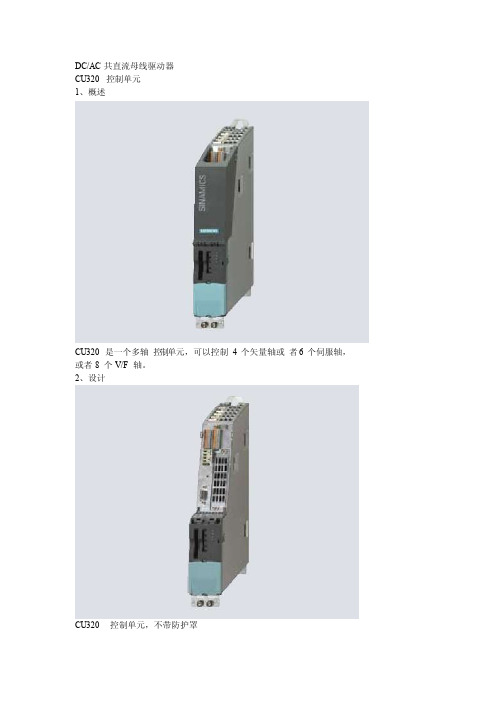
DC/AC共直流母线驱动器CU320控制单元1、概述CU320是一个多轴控制单元,可以控制4 个矢量轴或者6 个伺服轴,或者8 个V/F 轴。
2、设计CU320控制单元,不带防护罩控制器CU320 提供有下列接口:• 4 个DRIVE-CLiQ 插槽,可实现与其它DRIVE-CliQ 设备的通讯,例如电机模块、电源模块、传感器模块、终端模块• 1 个符合PRO FIBUS行规的PROFId riveV4 接口•8 点可参数化数字量输入(浮地式)•8 点可参数化双向数字量输入/数字量输出 ( 非浮地式),其中6 点快速数字量输入• 1 个RS232串行接口• 1 个基本操作面板B OP20 接口• 1 个CF 卡插槽• 1 个选件插槽(如TB30端子模块)• 3 个测试插座和一个参考接地• 1 个24 V DC 电源接口• 1 个PE ( 保护性接地)接口• 1 个地线接口由于固件和参数设置保存在CF 卡上,因此无需辅助工具就可更换控制器。
控制器CU320可安装在电源模块的侧面,也可以安装在控制柜的后壁上。
由于控制器 CU320的安装深度比电源模块要小一些,因此有相应的定位架可以提供,以便将控制器CU320的安装深度增加到270 mm。
3、集成在一个控制器CU320上可以连接 DRIVE-CLiQ 组件,比如电机模块和电源模块等。
模块的数量取决于所需要的性能。
在操作过程中,可将BOP20面板安装到CU320控制单元上进行诊断。
使用STARTER软件调试和诊断连接示例CU320控制单元。
- 1、下载文档前请自行甄别文档内容的完整性,平台不提供额外的编辑、内容补充、找答案等附加服务。
- 2、"仅部分预览"的文档,不可在线预览部分如存在完整性等问题,可反馈申请退款(可完整预览的文档不适用该条件!)。
- 3、如文档侵犯您的权益,请联系客服反馈,我们会尽快为您处理(人工客服工作时间:9:00-18:30)。
Mouser供货TI TUSB320 CC 逻辑和端口控制器
2015年10月26日–贸泽电子 (title="Mouser" target="_blank">Mouser Electronics) 即日起开始分销Texas Instruments (TI) 的USB Type-C™配置通道逻辑和端口控制器TUSB320系列。
TUSB320系列器件提供了USB Type-C配置通道 (CC) 逻辑和端口控制,支持系统探测插头的定向,并为终端设备确定适当的USB规范和模式设置。
Mouser分销的TI TUSB320器件可配置为下行数据端口 (DFP)、上行数据端口 (UFP) 或双角色数据端口 (DRP)。
该系列产品支持USB 2.0和USB3.1,使得设计人员能够在多个支持USB的设计中灵活运用这些器件。
TUSB320系列还具有多种特性(如模式配置和低待机电流),进而使得该器件可用于USB 2.0应用的灌/拉电流功能。
器件拥有宽电源范围 (2.7Vbus – 5.5Vbus) 并拥有低功耗的特性;其8 mW的低关断功率使各种电池供电应用大获裨益。
TUSB320系列产品提供了I2C或 GPIO控制、-40至 +85的工业级温度范围,并支持高达3A的电流通知和检测功能。
此器件可用于手机、平板电脑和USB外设中的主机、设备或双角色端口应用
Mouser同时备货的TUSB320EVM为TUSB320器件提供了评估平台。
此即插即用模块可通过板载DIP开关配置为工作在I2C或GPIO模式下的DFP、UFP或DRP端口。
Mouser拥有丰富的产品线与卓越的客服能力,通过提供先进技术的最新一代产品来满足设计工程师与采购人员的需求。
我们承诺以本地语言、本地货币提供本地客服和技术支持,通过全球21个客户支持中心为客户的最新设计项目提供全球最广泛的最新半导体及电子元件选择。
Mouser网站每日都会更新,用户可以查找超过1000万种产品,并能找到超过400万种可订购的物料编号以方便地进行在线采购。
同时为专家和初学者提供了业界首用的互动式目录、数据手册、特定供应商参考设计、应用笔记、技术设计信息和工程用工具。
关于贸泽电子 (Mouser Electronics)
Mouser是TTI的子公司,是沃伦巴菲特的伯克希尔哈撒韦的企业家族中的一员。
Mouser是一流的授权半导体和电子元件分销商,专门致力于以最快的方式向电子设计工程师和采购推广新产品和新技术。
网站有来自超过500家生产商的400多万种产品。
每年出版多语言版本产品目录为设计者提供现有最新的元件数据,以用于下一代的产品设计。
Mouser位于美国德州达拉斯南部,拥有最先进技术的49万2千平方英尺仓库向全球170个国家,超过50万家客户出货。