MBR4045WTG;MBR4045WT;中文规格书,Datasheet资料
MBR0540T1G;MBR0540T3G;NRVB0540T1G;中文规格书,Datasheet资料

January, 2012 − Rev. 7
1
Publication Order Number: MBR0540T1/D
/
MBR0540T1G, NRVB0540T1G, MBR0540T3G, NRVB0540T3G
*For additional information on our Pb−Free strategy and soldering details, please download the ON Semiconductor Soldering and Mounting Techniques Reference Manual, SOLDERRM/D.
i F, INSTANTANEOUS FORWARD CURRENT (AMPS)
IF, INSTANTANEOUS FORWARD CURRENT (AMPS)
10
100
10
25C
1.0 TJ = 125C TJ = -40C TJ = 25C TJ = 100C 0.1 0.2 0.4 0.6 0.8 1.0 1.2 vF, INSTANTANEOUS FORWARD VOLTAGE (VOLTS)
ELECTRICAL CHARACTERISTICS
Characteristic Maximum Instantaneous Forward Voltage (Note 3) (iF = 0.5 A) (iF = 1 A) Maximum Instantaneous Reverse Current (Note 3) (VR = 40 V) (VR = 20 V) 3. Pulse Test: Pulse Width 250 ms, Duty Cycle 2.0%. IR Symbol vF TJ = 25C 0.51 0.62 TJ = 25C 20 10 Value TJ = 100C 0.46 0.61 TJ = 100C 13,000 5,000 mA Unit V
MBRS140T3G;中文规格书,Datasheet资料

(Note: Microdot may be in either location)
Lead and Mounting Surface Temperature for Soldering Purposes:
ORDERING INFORMATION
Device MBRS140T3G SBRS8140T3G Package SMB (Pb−Free) SMB (Pb−Free) Shipping† 2,500 / Tape & Reel 2,500 / Tape & Reel
†For information on tape and reel specifications, including part orientation and tape sizes, please refer to our Tape and Reel Packaging Specifications Brochure, BRD8011/D.
DC
3 10
0
1
2
3
4
5
IF(AV), AVERAGE FORWARD CURRENT (AMPS)
Figure 5. Power Dissipation
3
/
MBRS140T3G, SBRS8140T3G
PACKAGE DIMENSIONS
Figure 3. Typical Capacitance
I F(AV) , AVERAGE FORWARD CURRENT (AMPS)
10 9 8 7 6 5 4 3 2 1 0 30 40 50 60 70 80 90 100 TC, CASE TEMPERATURE (C) 110 120 130
MBR1050;MBR1045;MBR1060;MBR1035;中文规格书,Datasheet资料
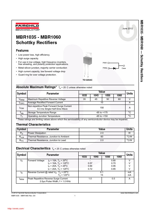
20 10 MBR1035-MBR1045
1
MBR1050-MBR1060
0.1
T A= 125ºC TA = 75º C
0.01
MBR1035-MBR1045
TA = 25º C
0.001 0
MBR1050-MBR1060
20
40
60
80 100 120
Percent of Rated Peak Reverse Voltage [%]
INDUCTIVE LOAD
2 .375" (9.00mm) LOAD
LENGTHS
0 0 25 50 75 100 125 150 175 Ambient Temperature [ºC]
Figure 1. Forward Current Derating Curve
Peak Forward Surge Current, IFSM [A]
0.5
Units
V V V V mA mA A
© 2012 Fairchild Semiconductor Corporation
MBR1035 - MBR1060 Rev. D0
1
/
MBR1035 - MBR1060 — Schottky Rectifie源自s354550
60
V
10
A
150
A
Tstg Storage Temperature Range
-65 to +175
°C
TJ Operating Junction Temperature
-65 to +150
°C
* These ratings are limiting values above which the serviceability of any semiconductor device may be impaired.
ASEMI肖特基二极管型号大全,找找MBR4045PT属于哪一类

编辑:GGASEMI肖特基二极管的型号众多,接下来所列型号主要以电流电压大小,分为大类,再以封装区分作为辅助分类。
ASEMI肖特基二极管型号大全,找找MBR4045PT属于哪一类1A~5A 20V~150V 肖特基二极管两者型号都在用SS封装:SS110 、SS14 。
10A 45V~200V 肖特基二极管采用TO-220AC封装的有:MBR10200AC、MBR10150AC、MBR10100AC、MBR1060AC、MBR1045AC、MBR1040AC采用TO-220封装的有:MBR1040FCT、MBR10200FCT、MBR10100FCT、MBR10150FCT、 MBR1040CT、MBR10200CT、MBR1040FCT、MBT1045FCT、 MBR1045CT、MBR1040CT、 MBR1045CT、MBR1060CT、MBR1060FCT、MBR10100CT、MBT10100FCT、MBR10150CT该封装有FCT和CT结尾的型号命名,区别于前者是塑封封装、后者是铁头封装。
采用TO-251封装的有:BD1045CT、BD1060CT、BD10100CT、BD10150CT、BD10200CT、BD1040CT采用TO-252封装的有:BD1040CS、BD1045CS、BD1060CS、BD10100CS、BD10150CS、 BD10200CS 采用TO-263封装的有:MBR10200DC、MBR1040DC、MBR1045DC、MBR1060DC、MBR10100DC、MBR10150DC20A 45V~200V肖特基二极管采用TO-220AC封装的有:MBR20200AC、MBR20150AC、MBR20100AC、MBR2060AC、 MR2045AC采用TO-251封装的有:BD2060CT、BD2045CT、BD20100CT、BD20150CT、BD20200CT、采用TO-252封装的有:BD20100CS、BD20150CS、BD20200CS、BD2045CS、BD2060CS采用TO-263封装的有:MBR2045DC、MBR2060DC、MBR20100DC、MBR20150DC、MBR20200DC采用TO-220封装的有:MBR2045CT、MBR2045FCT、MBR20200FCT、MBR2060CT、 MBR20100FCT、MBR2060FCT、MBR20100CT、MBR20100FCT、 MBR20150CT、MBR20150FCT、MBR20200CT、MBR20200FCT采用TO-247/3封装的有:MBR20200PT30A 45V~200V 肖特基二极管采用TO-247/3P封装的有:MBR3045PT、MBR3060PT、MBR30100PT、MBR30150PT、MBR30200PT采用TO-263封装的有:MBR30200DC、MBR3060DC、MBR30100DC、MBR30150DC、MBR3045DC采用TO-220封装的有:MBR3045CT、MBR3045FCT、MBR3060CT、MBR3060FCT、MBR30100CT、MBT30100FCT、MBR30150CT、MBR30150FCT、 MBR30200CT、MBR30200FCT 40A 45V~200V 肖特基二极管采用TO-263封装的有:MBR4045DC、MBR40200DC、MBR4060DC、MBR40100DC、MBR40150DC采用TO-247/3P封装的有:MBR40200PT、MBR4045PT、MBR4060PT、MBR40100PT、 MBR40150PT、采用TO-220封装的有:MBR4045FCT、MBR4045CT、MBR4060FCT、MB40100FCT、 MBR4060CT、MBR40100CT60A 45V~220V 肖特基二极管采用TO-247/3P封装的有:MBR6045PT、MBR6060PT、MBR60100PT、MBR60150PT、 MBR60200PT 10A~60A 20V~100V 肖特基二极管采用ITO-220AB封装的有:SBT10150UCT、SBT10100UCT、SBT1060UCT、SBT1045UCT、SBT10150VCT、SBT10100VCT、SBT1060VCT、SBT1045VCT、SBT30150UCT、SBT2045VCT、SBT2060VCT、SBT20100VCT、SBT20150VCT、SBT2045UCT、 SBT2060UCT、SBT20100UCT、 SBT20150UCT、SBT3045VCT、SBT3060VCT、SBT30100VCT、 SBT30150VCT、SBT3045UCT、SBT3060UCT、SBT30100UCT、SBT1045UFCT、SBT30100UFCT、SBT1060UFCT、SBT10150VFCT、SBT10100VFCT、SBT1060VFCT、SBT1045VFCT、SBT10100UFCT、SBT2045VFCT、SBT10150UFCT、 SBT2060VFCT、SBT20100VFCT、SBT20150VFCT、SBT2045UFCT、SBT2060UFCT、SBT20100UFCT、SBT20150UFCT、SBT3045VFCT、SBT3060VFCT、SBT30100VFCT、 SBT30150VFCT、SBT3045UFCT、SBT3060UFCT、SBT30150UFCT、SBT1045UFCT、 SB10100LCT、SB10150LCT、SB1045LFCT、SB1045LFCT、SB30100LFCT、 SB1060LFCT、SB30150LFCT、SB10100LFCT、SB2045LFCT、SB10150LFCT、SB2060LFCT、SB20100LFCT、SB3060LCT采用TO-220AB封装的有:SB1060LCT、SB30150LCT、SB30150LCT、SB10100LCT、SB2060LCT、SB10150LCT、SB20150LCT、SB3060LCT、SB30100LCT、SB1045LCT采用TO-277封装的有:10V45这款肖特基二极管型号是超低压降、贴片小封装的。
常用肖特基二极管参数

常用肖特基二极管参数型号制造商封装 If/A Vrrm/V 最大Vf/V1SS294 TOS SC-59 0.140 0.60BAT15-099 INF SOT143 0.11 40.32BAT54A PS SOT23 0.20 30 0.5010MQ060N IR SMA 0.7790 0.6510MQ100N IR SMA 0.77 100 0.9610BQ015 IR SMB 1.0015 0.34SS12 GS DO214 1.0020 0.50MBRS130LT3 ON - 1.0030 0.3910BQ040 IR SMB 1.0040 0.53RB060L-40 ROHM PMDS 1.00 40 0RB160L-40 ROHM PMDS 1.00 400.55SS14 GS DO214 1.0040 0.5MBRS140T3 ON - 1.0040 0.10BQ060 IR SMB 1.0060 0.57SS16 GS DO214 1.0060 0.7510BQ100 IR SMB 1.00 100 0.78MBRS1100T3 ON - 1.00 100 0.7510MQ040N IR SMA 1.10 40 0.5115MQ040N IR SMA 1.7040 0.55PBYR245CT PS SOT223 2.00 450.4530BQ015 IR SMC 3.0015 0.3530BQ040 IR SMC 3.0040 0.5130BQ060 IR SMC 3.0060 0.5830BQ100 IR SMC 3.00100 0.79STPS340U STM SOD6 3.00 40 0.84MBRS340T3 ON - 3.0040 0.52RB051L-40 ROHM PMDS 3.00 400.45MBRS360T3 ON - 3.0060 0.7030WQ04FN IR DPAK 3.3040 0.6230WQ06FN IR DPAK 3.30 60 0.7030WQ10FN IR DPAK 3.30 100 0.9130WQ03FN IR DPAK 3.50 30 0.5250WQ03FN IR DPAK 5.50 30 0.5350WQ06FN IR DPAK 5.50 60 0.576CWQ06FN IR DPAK 6.60 60 0.586CWQ10FN IR DPAKpr 6.60 100 0.811N5817 ON 轴向 1.00 20 0.751N5818 ON 轴向 1.00 30 0.55SB130 GS 轴向 1.00 30 0.50 1N5819 ON 轴向 1.00 40 0.60 MBR150 ON 轴向 1.00 50 1.00 MBR160 ON 轴向 1.00 60 1.00 11DQ10 IR 轴向 1.10 100 0.8511DQ04 IR 轴向 1.10 40 0.5511DQ05 IR 轴向 1.10 50 0.5811DQ06 IR 轴向 1.10 60 0.58MBRS340TR IR SMC 3.0040 0.431N5820 ON 轴向 3.00 20 0.851N5821 ON 轴向 3.00 30 0.381N5822 ON 轴向 3.00 40 0.52MBR360 ON 轴向 3.00 60 1.00SS32 GS DO214 3.0020 3.00SS34 GS DO214 3.0040 0.5031DQ10 IR DO201 3.30 100 0.85SB530 GS 轴向 5.00 30 0.57SB540 GS DO201 5.0040 0.5750SQ080 IR 轴向 5.00 80 0.6650SQ100 IR 轴向 5.00 100 0.66MBR735 GS TO220 7.5035 0.84MBR745 GS TO220 7.5045 0.84MBR745 IR TO220 7.5045 0.8480SQ040 IR 轴向 8.00 40 0.53STQ080 IR TO220 8.0080 0.728TQ100 TO220 8.00 100 0.7280SQ040 IR 轴向 8.00 40 0.5380SQ035 IR DO204AR 8.00 3 5 0.53HFA16PA60C IR TO247CT 8.00 6001.7095SQ015 轴向 9.00 15 0.3190SQ040 轴向 9.00 40 0.4810TQ045 TO220 10.0045 0.57MBR1035 GS TO220 10.0035 0.84MBR1045 ON TO220 10.0045 0.84STPS1045F ON ISO220 10.00 450.64MBR2060CT ON TO220 10.00 600.85MBR1060 ON TO220 10.0060 0.95PBYR10100 PS TO220 10.00 10 0 0.7010TQ040 IR TO220 10.0040 0.57MBR1045 IR TO220 10.0045 0.8410CTQ150-1 IR D2pak 10.00 15 0 0.7340L15CTS IR D2pak 10.00150 0.4185CNQ015A IR D61 80.0015 0.32150K40A IR D08 150.00400 1.3312CTQ040 IR TO220 12.00 450.73MBR1545CT IR TO220pr 15.00 45 0.72MBR1660 GS TO220 16.00 60 0.7516CTQ080 IR TO220pr 16.00 80 0.7216CTQ100 IR TO220pr 16.00 100 0.7216CTQ100-1 IR D2Pak 16.00 1000.7218TQ045 ON TO220 18.0045 0.60HFA16PB120 IR TO247 16.00 12003.00MBR1645 IR TO220AC 16.00 450.6319CTQ015 IR TO220 19.00 150.3620CTQ045 IR TO220pr 20.00 45 0.6420TQ045 IR TO220 20.0045 0.57MBR2045CT IR TO220pr 20.00 45 0.84MBR2090CT IR TO220pr 20.00 90 0.80MBR20100CT IR TO220pr 20.00 100 0.80MBR20100CT-1IR TO262 20.00 1000.80MBR2080CT IR TO220AB 20.00 800.85MBR2545CT IR TO220AB 30.00 450.82MBR3045WT IR TO247 30.00 4532CTQ030 IR TO220pr 30.00 30 0.4932CTQ303-1 IR D2Pak 30.00 300.4930CPQ060 IR TO220pr 30.00 60 0.6230CPQ080 IR TO247AC 30.00 800.8630CPQ100 IR TO247pr 30.00 100 0.8630CPQ150 IR TO247pr 30.00 150 1.0040CPQ040 IR TO247pr 40.00 40 0.4940CPQ045 IR TO247pr 40.00 45 0.4940CPQ050 IR TO247AA 40.00 500.5340CPQ100 IR TO247pr 40.00 100 0.7740L15CT IR TO220AB 40.00 150.5347CTQ020 IR TO220 40.00 200.3448CTQ060 IR TO220 40.00 600.5840L15CW IR TO247 40.0015 0.5242CTQ030 IR TO220 40.00 300.3840CTQ045 IR TO220 40.00 450.6840L45CW IR TO247 40.0045 0.7040CPQ060 ON TO247 40.00 600.68MBR4045WT IR TO247 40.00 450.59MBR4060WT IR TO247 40.00 600.7743CTQ100 IR TO220 40.00 10 0 0.9852CPQ030 IR TO247 50.0030 0.38MBR6045WT IR TO247pr 60.00 450.73STPS6045CPI ON TOP3I 60.00 450.8465PQ015 IR TO247 65.0015 0.5072CPQ030 IR TO247AC 70.00 300.5185CNQ015 IR D61 80.0015 0.3283CNQ100 IR D61 80.00100 0.6780CPQ020 IR TO247 80.0020 0.3282CNQ030A IR D61 80.0030 0.3782CNQ045A IR D61 80.0045 0.4783CNQ100A IR D61 80.00100 0.67120NQ045 IR HALFPAK 120.00 450.52125NQ015 IR D67 120.0015 0.33122NQ030 IR D67 120.0030 0.41STPS16045TV ON ISOTOP 160.00 450.95182NQ030 IR D67 180.0030 0.41200CNQ040 IR TO244AB 200.00 400.54200CNQ045 IR TO244AB 200.00 450.54200CNQ030 IR TO244AB 200.00 300.48STPS24045TV ON ISOTOP 240.00 450.91203CMQ080 IR TO244 200.00 8 0 1.03240NQ045 IR HALFPAK 240.00 450.55301CNQ045 IR TO244 300.00 4 5 0.59403CNQ100 IR TO244AB 400.00 1000.83440CNQ030 IR TO244AB 440.00 300.41(注:素材和资料部分来自网络,供参考。
MBR4045BT中文资料
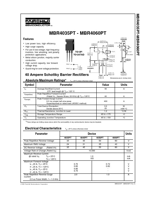
MBR4035PT-MBR4060PTMBR4035PT - MBR4060PT, Rev. A©1999 Fairchild Semiconductor CorporationTO-3P/TO-247ADMBR4035PT - MBR4060PT, Rev. ATRADEMARKSACEx™CoolFET™CROSSVOLT™E 2CMOS TM FACT™FACT Quiet Series™FAST ®FASTr™GTO™HiSeC™The following are registered and unregistered trademarks Fairchild Semiconductor owns or is authorized to use and is not intended to be an exhaustive list of all such trademarks.LIFE SUPPORT POLICYFAIRCHILD’S PRODUCTS ARE NOT AUTHORIZED FOR USE AS CRITICAL COMPONENTS IN LIFE SUPPORTDEVICES OR SYSTEMS WITHOUT THE EXPRESS WRITTEN APPROV AL OF FAIRCHILD SEMICONDUCTOR CORPORA TION.As used herein:ISOPLANAR™MICROWIRE™POP™PowerTrench™QS™Quiet Series™SuperSOT™-3SuperSOT™-6SuperSOT™-8TinyLogic™1. Life support devices or systems are devices or systems which, (a) are intended for surgical implant intothe body, or (b) support or sustain life, or (c) whosefailure to perform when properly used in accordancewith instructions for use provided in the labeling, can be reasonably expected to result in significant injury to the user.2. A critical component is any component of a lifesupport device or system whose failure to perform can be reasonably expected to cause the failure of the life support device or system, or to affect its safety or effectiveness.PRODUCT STATUS DEFINITIONS Definition of TermsDatasheet Identification Product Status Definition Advance InformationPreliminary No Identification Needed Obsolete This datasheet contains the design specifications for product development. Specifications may change in any manner without notice.This datasheet contains preliminary data, andsupplementary data will be published at a later date.Fairchild Semiconductor reserves the right to make changes at any time without notice in order to improve design.This datasheet contains final specifications. Fairchild Semiconductor reserves the right to make changes at any time without notice in order to improve design.This datasheet contains specifications on a product that has been discontinued by Fairchild semiconductor.The datasheet is printed for reference information only.Formative or In DesignFirst ProductionFull ProductionNot In ProductionDISCLAIMERFAIRCHILD SEMICONDUCTOR RESERVES THE RIGHT TO MAKE CHANGES WITHOUT FURTHER NOTICE TO ANY PRODUCTS HEREIN TO IMPROVE RELIABILITY , FUNCTION OR DESIGN. FAIRCHILD DOES NOT ASSUME ANY LIABILITY ARISING OUT OF THE APPLICATION OR USE OF ANY PRODUCT OR CIRCUIT DESCRIBED HEREIN; NEITHER DOES IT CONVEY ANY LICENSE UNDER ITS PATENT RIGHTS, NOR THE RIGHTS OF OTHERS.。
MBRB40250TG;中文规格书,Datasheet资料
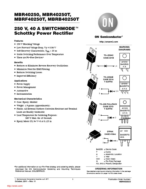
MBR40250, MBR40250T, MBRF40250T, MBRB40250T
TYPICAL CHARACTERISTICS
100
100
IF, MAXIMUM FORWARD CURRENT (A)
TJ = 150°C
TJ = 125°C 10
TJ = 100°C TJ = 25°C
TJ = 150°C
• Power Supply • Power Management • Automotive • Instrumentation
Mechanical Characteristics
• Case: Epoxy, Molded • Weight: 1.9 grams (approximately) • Finish: All External Surfaces Corrosion Resistant and Terminal
AKA
1 3
4
D2PAK
CASE 418AJ
1
4 3
AY WW
B40250TG AKA
*For additional information on our Pb−Free strategy and soldering details, please download the ON Semiconductor Soldering and Mounting Techniques Reference Manual, SOLDERRM/D.
Benefits
• Reduces or Eliminates Reverse Recovery Oscillations • Minimizes Need for EMI Filtering • Reduces Switching Losses • Improved Efficiency
MBR4045中文资料
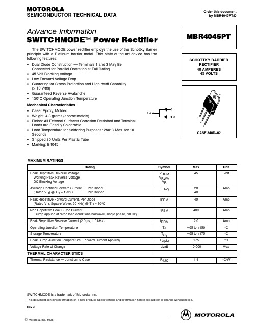
C, CAPACITANCE (pF)
1000
100
1
10 VR, REVERSE VOLTAGE (VOLTS)
100
110
120 130 140 TC, CASE TEMPERATURE (°C)
150
160
Figure 3. Typical Capacitance Per Leg
Figure 4. Current Derating Per Leg
TC = 25°C
TC = 100°C 1 100
TC = 25°C 800 0.01 0 10 20 30 VR, REVERSE VOLTAGE (VOLTS) 40 50
200 300 400 500 600 700 vF, INSTANTANEOUS FORWARD VOLTAGE (mV)
3
元器件交易网 MBR4045PT
Motorola reserves the right to make changes without further notice to any products herein. Motorola makes no warranty, representation or guarantee regarding the suitability of its products for any particular purpose, nor does Motorola assume any liability arising out of the application or use of any product or circuit, and specifically disclaims any and all liability, including without limitation consequential or incidental damages. “Typical” parameters which may be provided in Motorola data sheets and/or specifications can and do vary in different applications and actual performance may vary over time. All operating parameters, including “Typicals” must be validated for each customer application by customer’s technical experts. Motorola does not convey any license under its patent rights nor the rights of others. Motorola products are not designed, intended, or authorized for use as components in systems intended for surgical implant into the body, or other applications intended to support or sustain life, or for any other application in which the failure of the Motorola product could create a situation where personal injury or death may occur. Should Buyer purchase or use Motorola products for any such unintended or unauthorized application, Buyer shall indemnify and hold Motorola and its officers, employees, subsidiaries, affiliates, and distributors harmless against all claims, costs, damages, and expenses, and reasonable attorney fees arising out of, directly or indirectly, any claim of personal injury or death associated with such unintended or unauthorized use, even if such claim alleges that Motorola was negligent regarding the design or manufacture of the part. Motorola and are registered trademarks of Motorola, Inc. Motorola, Inc. is an Equal Opportunity/Affirmative Action Employer. Mfax is a trademark of Motorola, Inc. How to reach us: USA / EUROPE / Locations Not Listed: Motorola Literature Distribution; P.O. Box 5405, Denver, Colorado 80217. 1–303–675–2140 or 1–800–441–2447 Customer Focus Center: 1–800–521–6274 Mfax™: RMFAX0@ – TOUCHTONE 1–602–244–6609 ASIA/PACIFIC: Motorola Semiconductors H.K. Ltd.; 8B Tai Ping Industrial Park, Motorola Fax Back System – US & Canada ONLY 1–800–774–1848 51 Ting Kok Road, Tai Po, N.T., Hong Kong. 852–26629298 – /mfax/ HOME PAGE: /sps/ JAPAN: Nippon Motorola Ltd.: SPD, Strategic Planning Office, 4–32–1, Nishi–Gotanda, Shinagawa–ku, Tokyo 141, Japan. 81–3–5487–8488
SBR4045CT中文资料

40A SBR®Super Barrier RectifierFeatures MechanicalData• Case Material: Molded Plastic, UL FlammabilityClassification Rating 94V-0• Moisture Sensitivity: Level 1 per J-STD-020C• Terminals: Matte Tin Finish annealed overCopper leadframe. Solderable per MIL-STD-202,Method 208• Marking: See Page 3• Ordering Information: See Page 3• Low Forward Voltage Drop• Excellent High Temperature Stability• Super Barrier Design• Soft, Fast Switching Capability• Molded Plastic TO-220AB,and ITO-220AB packages• Lead Free Finish, RoHS Compliant (Note 2)Maximum Ratings @ T A = 25ºC unless otherwise specifiedSingle phase, half wave, 60Hz, resistive or inductive load.For capacitive load, derate current by 20%.Characteristic SymbolValueUnit Peak Repetitive Reverse VoltageWorking Peak Reverse VoltageDC Blocking VoltageV RRMV RWMV RM45 VRMS Reverse Voltage V R(RMS)32 VAverage Rectified Output Current @T C = 110ºC I O40 ANon-Repetitive Peak Forward Surge Current 8.3msSingle Half Sine-Wave Superimposed on Rated LoadI FSM280 APeak Repetitive Reverse Surge Current (2uS-1Khz) I RRM 2 AMaximum Thermal Resistance (per leg)Package = TO-220ABPackage = ITO-220ABRӨJC 24°C/WOperating and Storage Temperature Range T J, T STG-65 to +150 ºCElectrical Characteristics@ T A = 25ºC unless otherwise specifiedCharacteristic SymbolMin Typ Max Unit Test ConditionReverse Breakdown Voltage (Note 1) V(BR)R45 - - V I R = 0.5 mAForward Voltage Drop V F--0.470.550.50VI F = 20A, T J = 25ºCI F = 20A,T J = 125ºCLeakage Current (Note 1) I R- -0.5100mAV R = 45V, T J= 25 ºCV R = 45V, T J = 125 ºCNotes:1. Short duration pulse test used to minimize self-heating effect.2. RoHS revision 13.2.2003. High temperature solder exemption applied, see EU Directive Annex Note 7.__________SBR is a registered trademark of Diodes Incorporated.Package Outline DrawingsTO-220AB ITO-220ABTO-220ABDIM. MIN. MAX.A 4.47 4.67b 0.71 0.91b1 1.17 1.37c 0.31 0.53D 14.65 15.35D1 8.50 8.90E 10.01 10.31e 2.54type1 4.98 5.18F 1.17 1.37J1 2.52 2.82L 13.40 13.80L1 3.56 3.96ØP 3.735 3.935Q 2.59 2.89All Dimensions in MillimetersITO-220ABDIM. MIN. MAX.A 4.30 4.70b 0.50 0.75b1 1.10 1.35b2 1.50 1.75c 0.50 0.75D 14.80 15.20E 9.96 10.36e 2.54typF 2.80 3.20J1 2.50 2.90L 12.80 13.60L1 1.70 1.90ØP 3.50typQ 2.70typAll Dimensions in MillimetersMarking, Polarity, Weight & Ordering InformationSBR4045CT SBR4045CTFP Case StyleTO-220AB ITO-220ABtAnodeCommonCathode AnodePolarityCasetAnodeCommonCathode AnodeMarking2.1g 1.9gWeightOrderingInformationSBR4045CT SBR4045CTFP50 pieces/tube50 pieces/tubeYY = Last two digits of year, ex = 06 = 2006Date CodeWW = Week (01-52)Other MarkingInformationA = Foundry CodeB = Assembly CodeIMPORTANT NOTICEDiodes Incorporated and its subsidiaries reserve the right to make modifications, enhancements, improvements, corrections or other changeswithout further notice to any product herein. Diodes Incorporated does not assume any liability arising out of the application or use of any productdescribed herein; neither does it convey any license under its patent rights, nor the rights of others. The user of products in such applications shallassume all risks of such use and will agree to hold Diodes Incorporated and all the companies whose products are represented on our website,harmless against all damages.LIFE SUPPORTDiodes Incorporated products are not authorized for use as critical components in life support devices or systems without the expressed writtenapproval of the President of Diodes Incorporated.。
MBR4040PT中文资料

2 of 2
MBR4030PT - MBR4060PT
Forward Voltage Drop
Peak Reverse Current at Rated DC Blocking Voltage Typical Junction Capacitance
@ IF = 20A, TC = 25°C @ IF = 20A, TC = 125°C
@ TC = 25°C @ TC = 125°C
Single phase, half wave, 60Hz, resistive or inductive load. For capacitive load, derate current by 20%.
Characteristic
Peak Repetitive Reverse Voltage Working Peak Reverse Voltage DC Blocking Voltage
IFSM
VFM
IRM Cj RqJc dV/dt Tj, TSTG
MBR 4030PT
30
21
MBR MBR MBR 4035PT 4040PT 4045PT
35
40
45
24.5
28
31.5
40
400
0.70 0.60
1.0 100 1100 1.4 10,000 -65 to +150
MBR MBR 4O50PT 4060PT
RMS Reverse Voltage
Average Rectified Output Current
@ TC = 125°C (Note 1)
Non-Repetitive Peak Forward Surge Current
MBR40100PT中文资料
10 0
I n t a t a eu Fr a d r r Fn - I s n no s o w u r C et
T =1 5C 7° J 1 0 T =1 5C 2° J T= 2 ° 5C J
o aa nC ci t ace C p) p n - ( F T
R v ene m e t r I rs ( C - ue
元器件交易网
MBR40100PT
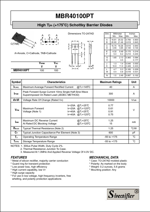
High Tjm (+175oC) Schottky Barrier Diodes
A C(TAB) A C A C A Dimensions TO-247AD
Dim. A B C D E F G H Millimeter Min. Max. 19.81 20.32 20.80 21.46 15.75 16.26 3.55 3.65 4.32 5.4 1.65 1.0 10.8 4.7 0.4 1.5 5.49 6.2 2.13 4.5 1.4 11.0 5.3 0.8 2.49 Inches Min. Max. 0.780 0.819 0.610 0.140 0.170 0.212 0.065 0.040 0.426 0.185 0.016 0.087 0.800 0.845 0.640 0.144 0.216 0.244 0.084 0.177 0.055 0.433 0.209 0.031 0.102
1 8
Rth C(D ) =1 5 C C .2 ° /W J
D=0 8 .0 1 D=0 7 6 .1 D=0 5 .2 1 4 D=0 3 .3 .5 1 D=0 0 2 1 0 M im 8 R SL it 6 4 2 D C
5
1 0
1 5
2 0
MBRB3045CT-1G;MBR3045STG;MBR3045ST;中文规格书,Datasheet资料

MBR3045ST,MBRB3045CT-1SWITCHMODE ™Power RectifierFeatures and Benefits•Dual Diode Construction — Terminals 1 and 3 May Be Connected for Parallel Operation at Full Rating •45 V Blocking V oltage •Low Forward V oltage Drop•175°C Operating Junction Temperature •Pb −Free Packages are AvailableApplications•Power Supply − Output Rectification •Power Management •InstrumentationMechanical Characteristics•Case: Epoxy, Molded•Weight (Approximately):1.9 Grams (TO −220AB)1.5 Grams (TO −262)•Finish: All External Surfaces Corrosion Resistant and Terminal Leads are Readily Solderable•Lead Temperature for Soldering Purposes:260°C Max. for 10 Seconds•Epoxy Meets UL 94 V −0 @ 0.125 inMAXIMUM RATINGSRatingSymbol Value Unit Peak Repetitive Reverse Voltage Working Peak Reverse Voltage DC Blocking Voltage V RRM V RWM V R 45VAverage Rectified Current Per Device (T C = 130°C)Per DiodeI F(AV)3015A Peak Repetitive Forward Current, per Diode (Square Wave, V R = 45 V, 20 kHz)I FRM 30A Non −Repetitive Peak Surge Current (Surge Applied at Rated Load Conditions,Halfwave, Single Phase, 60 Hz)IFSM150APeak Repetitive Reverse Current, per Diode (2.0 m s, 1.0 kHz)I RRM 2.0A Storage Temperature RangeT stg −65 to +175°C Operating Junction Temperature (Note 1)T J −65 to +175°C Peak Surge Junction Temperature (Forward Current Applied)T J(pk)175°CVoltage Rate of Change (Rated V R )dv/dt10,000V/m sStresses exceeding Maximum Ratings may damage the device. MaximumRatings are stress ratings only. Functional operation above the Recommended Operating Conditions is not implied. Extended exposure to stresses above the Recommended Operating Conditions may affect device reliability.1.The heat generated must be less than the thermal conductivity from Junction −to −Ambient: dP D /dT J < 1/R q JA .TO −220AB CASE 221A STYLE 6SCHOTTKY BARRIERRECTIFIER 30 AMPERES 45 VOLTS312, 4MARKING DIAGRAMSA = Assembly Location Y = YearWW = Work WeekAKA = Polarity Designator G = Pb −Free DeviceI 2PAK (TO −262)CASE 418D PLASTICAYWW B3045CTG AKASee detailed ordering and shipping information in the package dimensions section on page 3 of this data sheet.ORDERING INFORMATIONTHERMAL CHARACTERISTICS (Per Diode)CharacteristicSymbol Value Unit Thermal Resistance, Junction to CaseR θJC1.5°C/WELECTRICAL CHARACTERISTICS (Per Diode)Instantaneous Forward Voltage (Note 2)(i F = 15 Amp, T C = 25°C)(i F = 15 Amp, T C = 125°C)(i F = 30 Amp, T C = 25°C)(i F = 30 Amp, T C = 125°C)v F0.620.570.760.72VoltsInstantaneous Reverse Current (Note 2)(V R = 45 Volts, T C = 25°C)(V R = 45 Volts, T C = 125°C)I R0.240mA2Pulse Test: Pulse Width = 300 μs, Duty Cycle ≤ 2.0%Figure 1. Typical Forward VoltageFigure 2. Maximum Reverse Currentv F , INSTANTANEOUS FORWARD VOLTAGE (VOLTS)100010V R , REVERSE VOLTAGE (VOLTS)0.20.040.02i F , I N S T A N T A N E O U S F O R W A R D C U R R E N T (A M P S )I 1.00.10.41.00.1, R E V E R S E C U R R E N T (m A )R 4.02.01020100402001000.01Figure 3. Typical Reverse Currentv F , MAXIMUM FORWARD VOLTAGE (VOLTS)100010i F , M A X I M U M F O R W A R D C U R R E N T (A M P S )1.00.1100Figure 4. Current Derating, Case Figure 5. Current Derating, AmbientFigure 6. Forward Power Dissipation 110T C , CASE TEMPERATURE (°C)208.04.00T A , AMBIENT TEMPERATURE (°C)2024168.0040I F , AVERAGE FORWARD CURRENT (AMPS)3216128.04.00I I F (A V ), A V E R A G E F O R W A R D C U R R E N T (A M P S )1201301401706080180P 28, A V E R A G E F O R W A R D C U R R E N T (A M P S )F (A V )202416122420124.0100120140, A V E R A G E P O W E R D I S S I P A T I O N (W A T T S )F (A V )Figure 7. Capacitance0V R , REVERSE VOLTAGE (V)100010103040C , C A P A C I T A N C E (p F )100501000020150160160ORDERING INFORMATIONDevicePackage Shipping MBR3045ST TO −22050 Units/Rail MBR3045STG TO −220(Pb −Free)50 Units/Rail MBRB3045CT −1TO −26250 Units/Rail MBRB3045CT −1GTO −262(Pb −Free)50 Units/RailTO −220CASE 221A −09ISSUE AFNOTES:1.DIMENSIONING AND TOLERANCING PER ANSI Y14.5M, 1982.2.CONTROLLING DIMENSION: INCH.3.DIMENSION Z DEFINES A ZONE WHERE ALL BODY AND LEAD IRREGULARITIES ARE ALLOWED.STYLE 6:PIN 1.ANODE 2.CATHODE 3.ANODE 4.CATHODEDIM MIN MAX MIN MAX MILLIMETERS INCHES A 0.5700.62014.4815.75B 0.3800.4059.6610.28C 0.1600.190 4.07 4.82D 0.0250.0350.640.88F 0.1420.161 3.61 4.09G 0.0950.105 2.42 2.66H 0.1100.155 2.80 3.93J 0.0140.0250.360.64K 0.5000.56212.7014.27L 0.0450.060 1.15 1.52N 0.1900.210 4.83 5.33Q 0.1000.1202.543.04R 0.0800.110 2.04 2.79S 0.0450.0551.15 1.39T 0.2350.255 5.97 6.47U 0.0000.0500.00 1.27V 0.045--- 1.15---Z---0.080--- 2.04FSEATINGPLANEI 2PAK (TO −262)CASE 418D −01ISSUE DNOTES:1.DIMENSIONING AND TOLERANCING PER ANSI Y14.5M, 1982.2.CONTROLLING DIMENSION: INCH.D DIM MIN MAX MIN MAX MILLIMETERSINCHES A 0.3350.3808.519.65B 0.3800.4069.6510.31C 0.1600.185 4.06 4.70D 0.0260.0350.660.89E 0.0450.055 1.14 1.40G 0.100 BSC 2.54 BSC H 0.0940.110 2.39 2.79J 0.0130.0250.330.64S 0.390 REF 9.90 REF V 0.0450.070 1.14 1.78W0.5220.55113.2514.00MBM 0.13 (0.005)T F 0.122 REF 3.10 REF K 0.5000.56212.7014.27ON Semiconductor and are registered trademarks of Semiconductor Components Industries, LLC (SCILLC). SCILLC reserves the right to make changes without further notice to any products herein. SCILLC makes no warranty, representation or guarantee regarding the suitability of its products for any particular purpose, nor does SCILLC assume any liability arising out of the application or use of any product or circuit, and specifically disclaims any and all liability, including without limitation special, consequential or incidental damages.“Typical” parameters which may be provided in SCILLC data sheets and/or specifications can and do vary in different applications and actual performance may vary over time. All operating parameters, including “Typicals” must be validated for each customer application by customer’s technical experts. SCILLC does not convey any license under its patent rights nor the rights of others. SCILLC products are not designed, intended, or authorized for use as components in systems intended for surgical implant into the body, or other applications intended to support or sustain life, or for any other application in which the failure of the SCILLC product could create a situation where personal injury or death may occur. Should Buyer purchase or use SCILLC products for any such unintended or unauthorized application, Buyer shall indemnify and hold SCILLC and its officers, employees, subsidiaries, affiliates,and distributors harmless against all claims, costs, damages, and expenses, and reasonable attorney fees arising out of, directly or indirectly, any claim of personal injury or death associated with such unintended or unauthorized use, even if such claim alleges that SCILLC was negligent regarding the design or manufacture of the part. SCILLC is an Equal Opportunity/Affirmative Action Employer. This literature is subject to all applicable copyright laws and is not for resale in any manner.PUBLICATION ORDERING INFORMATIONSWITCHMODE is a trademark of Semiconductor Components Industries, LLC.分销商库存信息:ONSEMIMBRB3045CT-1G MBR3045STG MBR3045ST。
MBR140SFT1G;MBR140SFT3G;NRVB140SFT3G;NRVB140SFT1G;中文规格书,Datasheet资料

Mechanical Characteristics
** 8 mm Tape, 7” Reel *** 8 mm Tape, 13” Reel †For information on tape and reel specifications, including part orientation and tape sizes, please refer to our Tape and Reel Packaging Specifications Brochure, BRD8011/D.
Features
SCHOTTKY BARRIER RECTIFIER 1.0 AMPERES 40 VOLTS
SOD−123FL CASE 498 PLASTIC
MARKING DIAGRAM
Guardring for Stress Protection Low Forward Voltage 125C Operating Junction Temperature Epoxy Meets UL 94 V−0 @ 0.125 in Package Designed for Optimal Automated Board Assembly ESD Rating: Human Body Model = 3B Machine Model = C AEC−Q101 Qualified and PPAP Capable NRVB Prefix for Automotive and Other Applications Requiring Unique Site and Control Change Requirements All Packages are Pb−Free* Device Marking: L4F Polarity Designator: Cathode Band Weight: 11.7 mg (approximately) Case: Epoxy, Molded Finish: All External Surfaces Corrosion Resistant and Terminal Leads are Readily Solderable Lead and Mounting Surface Temperature for Soldering Purposes: 260C Max. for 10 Seconds
VFT4045BP-M34W;中文规格书,Datasheet资料

0.600 (15.24) 0.580 (14.73)
7° REF. 0.350 (8.89) 0.330 (8.38)
1
2 0.191 (4.85) 0.171 (4.35) 7° REF.
0.560 (14.22) 0.530 (13.46)
0.057 (1.45) 0.045 (1.14)
0.110 (2.79) 0.100 (2.54)
0.025 (0.64) 0.015 (0.38)
0.035 (0.89) 0.025 (0.64) 0.205 (5.21) 0.195 (4.95) 0.028 (0.71) 0.020 (0.51)
Document Number: 89456 3 For technical questions within your region: DiodesAmericas@, DiodesAsia@, DiodesEurope@ THIS DOCUMENT IS SUBJECT TO CHANGE WITHOUT NOTICE. THE PRODUCTS DESCRIBED HEREIN AND THIS DOCUMENT ARE SUBJECT TO SPECIFIC DISCLAIMERS, SET FORTH AT /doc?91000 /
Case Temperature (°C)
Fig. 1 - Maximum Forward Current Derating Curve
Instantaneous Forward Voltage (V) Fig. 2 - Typical Instantaneous Forward Characteristics
Reverse Voltage (V) Fig. 4 - Typical Junction Capacitance
MBR4045WT中文资料

Figure 1. Typical Forward Voltage
Figure 2. Typical Reverse Current
I F(AV), AVERAGE FORWARD CURRENT (AMPS)
10000
30 25 20 15 DC 10 5 0 100 SQUARE WAVE (VR = 45 V)
20 40 40 400 2.0 – 65 to +150 – 65 to +175 175 10,000
Amp Amp Amp Amp °C °C °C V/µs
THERMAL CHARACTERISTICS
Thermal Resistance — Junction to Case RθJC 1.4 °C/W
CASE 340K–01 ISSUE O
Rectifier Device Data
3
元器件交易网 MBR4045WT
Motorola reserves the right to make changes without further notice to any products herein. Motorola makes no warranty, representation or guarantee regarding the suitability of its products for any particular purpose, nor does Motorola assume any liability arising out of the application or use of any product or circuit, and specifically disclaims any and all liability, including without limitation consequential or incidental damages. “Typical” parameters which may be provided in Motorola data sheets and/or specifications can and do vary in different applications and actual performance may vary over time. All operating parameters, including “Typicals” must be validated for each customer application by customer’s technical experts. Motorola does not convey any license under its patent rights nor the rights of others. Motorola products are not designed, intended, or authorized for use as components in systems intended for surgical implant into the body, or other applications intended to support or sustain life, or for any other application in which the failure of the Motorola product could create a situation where personal injury or death may occur. Should Buyer purchase or use Motorola products for any such unintended or unauthorized application, Buyer shall indemnify and hold Motorola and its officers, employees, subsidiaries, affiliates, and distributors harmless against all claims, costs, damages, and expenses, and reasonable attorney fees arising out of, directly or indirectly, any claim of personal injury or death associated with such unintended or unauthorized use, even if such claim alleges that Motorola was negligent regarding the design or manufacture of the part. Motorola and are registered trademarks of Motorola, Inc. Motorola, Inc. is an Equal Opportunity/Affirmative Action Employer. Mfax is a trademark of Motorola, Inc. How to reach us: USA / EUROPE / Locations Not Listed: Motorola Literature Distribution; P.O. Box 5405, Denver, Colorado 80217. 1–303–675–2140 or 1–800–441–2447 Customer Focus Center: 1–800–521–6274 Mfax™: RMFAX0@ – TOUCHTONE 1–602–244–6609 ASIA/PACIFIC: Motorola Semiconductors H.K. Ltd.; 8B Tai Ping Industrial Park, Motorola Fax Back System – US & Canada ONLY 1–800–774–1848 51 Ting Kok Road, Tai Po, N.T., Hong Kong. 852–26629298 – /mfax/ HOME PAGE: /sps/ JAPAN: Nippon Motorola Ltd.: SPD, Strategic Planning Office, 4–32–1, Nishi–Gotanda, Shinagawa–ku, Tokyo 141, Japan. 81–3–5487–8488
MBRB4045CT
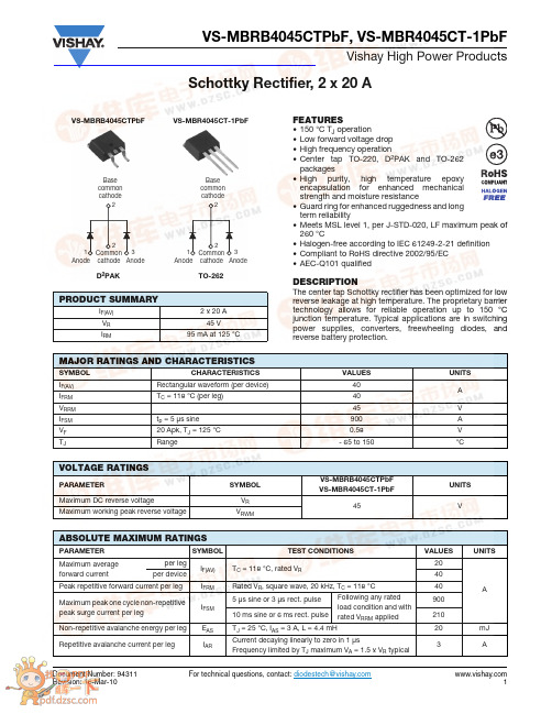
Document Number: 94311For technical questions, contact: diodestech@Schottky Rectifier, 2 x 20 AVS-MBRB4045CTPbF, VS-MBR4045CT-1PbFVishay High Power ProductsFEATURES•150 °C T J operation•Low forward voltage drop •High frequency operation•Center tap TO-220, D 2PAK and TO-262packages•High purity, high temperature epoxy encapsulation for enhanced mechanical strength and moisture resistance•Guard ring for enhanced ruggedness and long term reliability•Meets MSL level 1, per J-STD-020, LF maximum peak of 260 °C•Halogen-free according to IEC 61249-2-21 definition •Compliant to RoHS directive 2002/95/EC •AEC-Q101 qualifiedDESCRIPTIONThe center tap Schottky rectifier has been optimized for low reverse leakage at high temperature. The proprietary barrier technology allows for reliable operation up to 150 °C junction temperature. Typical applications are in switching power supplies, converters, freewheeling diodes, and reverse battery protection.PRODUCT SUMMARYI F(AV) 2 x 20 A V R 45 V I RM95 mA at 125 °CV S -MBRB4045CTP b FD 2PAKTO-262V S -MBR4045CT-1P b FBa s e common cathodeAnode Anode Common cathode 1322Ba s e common cathodeAnode AnodeCommon cathode 1322MAJOR RATINGS AND CHARACTERISTICSSYMBOL CHARACTERISTICSVALUES UNITS I F(AV)Rectangular waveform (per device)40A I FRM T C = 118 °C (per leg)40V RRM 45V I FSM t p = 5 μs sine 900A V F 20 Apk, T J = 125 °C 0.58V T JRange- 65 to 150°CVOLTAGE RATINGSPARAMETERSYMBOLVS-MBRB4045CTPbF VS-MBR4045CT-1PbFUNITS Maximum DC reverse voltageV R 45VMaximum working peak reverse voltageV RWMABSOLUTE MAXIMUM RATINGSPARAMETER SYMBOL TEST CONDITIONSVALUES UNITSMaximum average forward currentper leg I F(AV)T C = 118 °C, rated V R20A per device40Peak repetitive forward current per leg I FRM Rated V R , square wave, 20 kHz, T C = 118 °C 40Maximum peak one cycle non-repetitive peak surge current per legI FSM 5 μs sine or 3 μs rect. pulse Following any rated load condition and with rated V RRM applied90010 ms sine or 6 ms rect. pulse 210Non-repetitive avalanche energy per leg E AS T J = 25 °C, I AS = 3 A, L = 4.4 mH20mJ Repetitive avalanche current per legI ARCurrent decaying linearly to zero in 1 μsFrequency limited by T J maximum V A = 1.5 x V R typical3A 查询"VS-MBRB4045CTPbF, VS-MBR4045CT-1PbF"供应商 For technical questions, contact: diodestech@Document Number: 94311VS-MBRB4045CTPbF, VS-MBR4045CT-1PbFVishay High Power Products Schottky Rectifier, 2 x 20 A Note(1)Pulse width < 300 μs, duty cycle < 2 %ELECTRICAL SPECIFICATIONSPARAMETER SYMBOLTEST CONDITIONSVALUES UNITSMaximum forward voltage dropV FM (1)20 AT J = 25 °C 0.60V 40 A 0.7820 A T J = 125 °C0.5840 A0.75Maximum instantaneousreverse currentI RM (1)T J = 25 °CRated DC voltage1mA T J = 100 °C 50T J = 125 °C95Maximum junction capacitance C T V R = 5 V DC (test signal range 100 kHz to 1 MHz), 25 °C 900pF Typical series inductance L S Measured from top of terminal to mounting plane 8.0nH Maximum voltage rate of change dV/dtRated V R10 000V/μs THERMAL - MECHANICAL SPECIFICATIONSPARAMETERSYMBOLTEST CONDITIONSVALUES UNITS Maximum junction temperature range T J - 65 to 150°CMaximum storage temperature range T Stg - 65 to 175Maximum thermal resistance,junction to case per leg R thJC DC operation1.5°C/W Typical thermal resistance, case to heatsinkR thCS Mounting surface, smooth and greased (Only for TO-220)0.50Maximum thermal resistance, junction to ambient R thJADC operation(For D 2PAK and TO-262)50Approximate weight 2g 0.07oz.Mounting torque minimum Non-lubricated threads 6 (5)kgf · cm (lbf · in)maximum12 (10)Marking deviceCase style D 2PAK MBRB4045CT Case style TO-262MBR4045CT-1查询"VS-MBRB4045CTPbF, VS-MBR4045CT-1PbF"供应商Document Number: 94311For technical questions, contact: diodestech@Fig. 1 - Maximum Forward Voltage Drop Characteristics(Per Leg)Fig. 2 - Typical Values of Reverse Current vs.Reverse Voltage (Per Leg)Fig. 3 - Typical Junction Capacitance vs. Reverse Voltage (Per Leg)Fig. 4 - Maximum Thermal Impedance Z thJC Characteristics (Per Leg) For technical questions, contact: diodestech@Document Number: 94311VS-MBRB4045CTPbF, VS-MBR4045CT-1PbFVishay High Power Products Schottky Rectifier, 2 x 20 A Fig. 5 - Maximum Allowable Case Temperature vs.Average Forward CurrentFig. 6 - Forward Power Loss CharacteristicsFig. 7 - Maximum Non-Repetitive Surge Current (Per Leg)Note(1)Formula used: T C = T J - (Pd + Pd REV ) x R thJC ;Pd = Forward power loss = I F(AV) x V FM at (I F(AV)/D) (see fig. 6); Pd REV = Inverse power loss = V R1 x I R (1 - D); I R at V R1 = Rated V R查询"VS-MBRB4045CTPbF, VS-MBR4045CT-1PbF"供应商ORDERING INFORMATION TABLELINKS TO RELATED DOCUMENTSDimensions /doc?95014Part marking information /doc?95008Packaging information /doc?95032SPICE model /doc?95296Document Number: 94311For technical questions, contact: diodestech@ DisclaimerAll product specifications and data are subject to change without notice.Vishay Intertechnology, Inc., its affiliates, agents, and employees, and all persons acting on its or their behalf (collectively, “Vishay”), disclaim any and all liability for any errors, inaccuracies or incompleteness contained herein or in any other disclosure relating to any product.Vishay disclaims any and all liability arising out of the use or application of any product described herein or of any information provided herein to the maximum extent permitted by law. The product specifications do not expand or otherwise modify Vishay’s terms and conditions of purchase, including but not limited to the warranty expressed therein, which apply to these products.No license, express or implied, by estoppel or otherwise, to any intellectual property rights is granted by this document or by any conduct of Vishay.The products shown herein are not designed for use in medical, life-saving, or life-sustaining applications unless otherwise expressly indicated. Customers using or selling Vishay products not expressly indicated for use in such applications do so entirely at their own risk and agree to fully indemnify Vishay for any damages arising or resulting from such use or sale. Please contact authorized Vishay personnel to obtain written terms and conditions regarding products designed for such applications.Product names and markings noted herein may be trademarks of their respective owners.Document Number: 。
MBR4045PT

3
MBR4045PT
Motorola reserves the right to make changes without further notice to any products herein. Motorola makes no warranty, representation or guarantee regarding the suitability of its products for any particular purpose, nor does Motorola assume any liability arising out of the application or use of any product or circuit, and specifically disclaims any and all liability, including without limitation consequential or incidental damages. “Typical” parameters which may be provided in Motorola data sheets and/or specifications can and do vary in different applications and actual performance may vary over time. All operating parameters, including “Typicals” must be validated for each customer application by customer’s technical experts. Motorola does not convey any license under its patent rights nor the rights of others. Motorola products are not designed, intended, or authorized for use as components in systems intended for surgical implant into the body, or other applications intended to support or sustain life, or for any other application in which the failure of the Motorola product could create a situation where personal injury or death may occur. Should Buyer purchase or use Motorola products for any such unintended or unauthorized application, Buyer shall indemnify and hold Motorola and its officers, employees, subsidiaries, affiliates, and distributors harmless against all claims, costs, damages, and expenses, and reasonable attorney fees arising out of, directly or indirectly, any claim of personal injury or death associated with such unintended or unauthorized use, even if such claim alleges that Motorola was negligent regarding the design or manufacture of the part. Motorola and are registered trademarks of Motorola, Inc. Motorola, Inc. is an Equal Opportunity/Affirmative Action Employer. Mfax is a trademark of Motorola, Inc. How to reach us: USA / EUROPE / Locations Not Listed: Motorola Literature Distribution; P.O. Box 5405, Denver, Colorado 80217. 1–303–675–2140 or 1–800–441–2447 Customer Focus Center: 1–800–521–6274 Mfax™: RMFAX0@ – TOUCHTONE 1–602–244–6609 ASIA/PACIFIC: Motorola Semiconductors H.K. Ltd.; 8B Tai Ping Industrial Park, Motorola Fax Back System – US & Canada ONLY 1–800–774–1848 51 Ting Kok Road, Tai Po, N.T., Hong Kong. 852–26629298 – /mfax/ HOME PAGE: /sps/ JAPAN: Nippon Motorola Ltd.: SPD, Strategic Planning Office, 4–32–1, Nishi–Gotanda, Shinagawa–ku, Tokyo 141, Japan. 81–3–5487–8488
MBR2045CTG中文资料
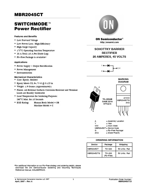
100 TJ = 150°C
10
125°C
100°C
1.0 75°C
0.1 25°C
0.01
0.001 0 5.0 10 15 20 25 30 35 40 45 50 VR, REVERSE VOLTAGE (VOLTS)
Figure 4. Maximum Reverse Current
IFSM, PEAK HALF−WAVE CURRENT (AMPS)
DTJL = Ppk • RqJL [D + (1 − D) • r(t1 + tp) + r(tp) − r(t1)] where: DTJL = the increase in junction temperature above the lead temperature. r(t) = normalized value of transient thermal resistance at time, t, i.e.:
Leads are Readily Solderable
• Lead Temperature for Soldering Purposes:
260°C Max. for 10 Seconds
• ESD Rating: Human Body Model = 3B
Machine Model = C
0.1
0.2
0.4
0.6
0.8
1.0
1.2
1.4
vF, INSTANTANEOUS VOLTAGE (VOLTS)
Figure 2. Maximum Forward Voltage
3
元器件交易网
MBR2045CT
IR, REVERSE CURRENT (mA)
- 1、下载文档前请自行甄别文档内容的完整性,平台不提供额外的编辑、内容补充、找答案等附加服务。
- 2、"仅部分预览"的文档,不可在线预览部分如存在完整性等问题,可反馈申请退款(可完整预览的文档不适用该条件!)。
- 3、如文档侵犯您的权益,请联系客服反馈,我们会尽快为您处理(人工客服工作时间:9:00-18:30)。
ON Semiconductor and
are registered trademarks of Semiconductor Components Industries, LLC (SCILLC). SCILLC reserves the right to make changes without further notice
Leads are Readily Solderable
• Lead Temperature for Soldering Purposes:
260°C Max. for 10 Seconds
• ESD Rating: Human Body Model 3B
Machine Model C
VF
V
−
0.52
0.70
−
0.47
0.60
−
0.65
0.80
−
0.63
0.75
Instantaneous Reverse Current (Note 2)
IR
@ Rated DC Voltage, TJ = 25°C
@ Rated DC Voltage, TJ = 100°C
2. Pulse Test: Pulse Width = 300 ms, Duty Cycle < 2.0%
10 TC = 150°C
1 100
TC = 100°C
TC = 25°C
200
300
400
500
600
700
vF, INSTANTANEOUS FORWARD VOLTAGE (mV)
Figure 1. Typical Forward Voltage
1
0.1
0.01
800
0
TC = 150°C TC = 100°C
Q 3.55 3.65 0.140 0.144
U
6.15 BSC
0.242 BSC
W 2.87 3.12 0.113 0.123
STYLE 2: PIN 1. ANODE 2. CATHODE (S) 3. ANODE 2 4. CATHODES (S)
SWITCHMODE is a trademark of Semiconductor Components Industries, LLC.
INCHES
DIM MIN MAX MIN MAX
A 20.32 21.08 0.800 8.30
B 15.75 16.26 0.620 0.640
C 4.70 5.30 0.185 0.209
D 1.00 1.40 0.040 0.055
E 1.90 2.60 0.075 0.102
F 1.65 2.13 0.065 0.084
TC = 25°C
10
20
30
40
50
VR, REVERSE VOLTAGE (VOLTS)
Figure 2. Typical Reverse Current
I F(AV), AVERAGE FORWARD CURRENT (AMPS)
10000 1000 100
1
30
25
20
15
DC
10
SQUARE WAVE
mA
−
0.09
1.0
−
7.5
50
/
2
iF, INSTANTANEOUS FORWARD CURRENT (AMPS)
MBR4045WT
TYPICAL ELECTRICAL CHARACTERISTICS
100
100
10
IR, REVERSE CURRENT (mA)
SCHOTTKY BARRIER RECTIFIER
40 AMPERES, 45 VOLTS
1 2, 4
3
1 2 3
TO−247AC CASE 340L
STYLE 2
MARKING DIAGRAM
MBR4045WT AYWWG
MBR4045WT = Device Code
A
= Assembly Location
(VR = 45 V)
5
10 VR, REVERSE VOLTAGE (VOLTS)
0
100
100
110
120
130
140
150 160
TC, CASE TEMPERATURE (°C)
Figure 3. Typical Capacitance Per Leg
Figure 4. Current Derating Per Leg
arising out of the application or use of any product or circuit, and specifically disclaims any and all liability, including without limitation special, consequential or incidental damages.
© Semiconductor Components Industries, LLC, 2010
1
March, 2010 − Rev. 8
/
ORDERING INFORMATION
Device MBR4045WT MBR4045WTG
Package
TO−247
TO−247 (Pb−Free)
G
5.45 BSC
0.215 BSC
H 1.50 2.49 0.059 0.098
J 0.40 0.80 0.016 0.031
K 19.81 20.83 0.780 0.820
L 5.40 6.20 0.212 0.244
N 4.32 5.49 0.170 0.216
P --- 4.50 --- 0.177
IRRM Tstg TJ TJ(pk)
2.0
A
−65 to +175
°C
−65 to +175
ห้องสมุดไป่ตู้
°C
175
°C
Voltage Rate of Change
dv/dt
10,000
V/ms
Stresses exceeding Maximum Ratings may damage the device. Maximum Ratings are stress ratings only. Functional operation above the Recommended Operating Conditions is not implied. Extended exposure to stresses above the Recommended Operating Conditions may affect device reliability. 1. The heat generated must be less than the thermal conductivity from Junction−to−Ambient: dPD/dTJ < 1/RqJA.
to any products herein. SCILLC makes no warranty, representation or guarantee regarding the suitability of its products for any particular purpose, nor does SCILLC assume any liability
THERMAL CHARACTERISTICS Characteristic
Maximum Thermal Resistance, Junction−to−Case Maximum Thermal Resistance, Junction−to−Ambient
Conditions Min. Pad Min. Pad
P −Y−
K
F 2 PL
W
G D 3 PL
J H
0.25 (0.010) M Y Q S
NOTES: 1. DIMENSIONING AND TOLERANCING PER ANSI Y14.5M, 1982. 2. CONTROLLING DIMENSION: MILLIMETER.
MILLIMETERS
Average Rectified Forward Current (Rated VR, TC = 125°C) Per Diode
Per Device
VRRM VRWM
VR
IF(AV)
45
V
A 20 40
Peak Repetitive Forward Current, (Rated VR, Square Wave, 20 kHz, TC = 90°C) Per Diode
Y
= Year
WW
= Work Week
G
= Pb−Free Package
*For additional information on our Pb−Free strategy and soldering details, please download the ON Semiconductor Soldering and Mounting Techniques Reference Manual, SOLDERRM/D.
MBR4045WT
SWITCHMODE™ Power Rectifier
Features and Benefits
• Low Forward Voltage • Low Power Loss/High Efficiency • High Surge Capacity • 175°C Operating Junction Temperature • 40 A Total (20 A Per Diode Leg) • Pb−Free Package is Available*
