刘聪:HTML5开发工具之英特尔XDK New解析
TPM Interface Specification (TIS)
7.1
Number of PCRs ................................................................................................................................. 19
7. PCR Requirements ......................................................................................................................................... 19
1.1
Terminology........................................................................................................................................... 7
TCG Published
Specification Version 1.2; Revision 1.00
Contents
1. TPM Requirements General Introduction ......................................................................................................... 7
Except that a license is hereby granted by TCG to copy and reproduce this specification for internal use only.
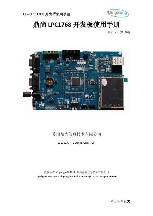
鼎尚 LPC1768 开发板使用手册
串行接口 以太网 MAC 带 RMII 接口和相关的 DMA 控制器; USB 2.0 全速从机/主机/OTG 控制器,带有用于从机、主机功能的片
内 PHY 和相关的 DMA 控制器; 4 个 UART、带小数波特率发生功能、内部 FIFO、DMA 支持和 RS-485
支持。1 个 UART 带有 modem 控制 IO 并支持 RS-485,全部的 UART 都支持 IrDA; CAN 控制器,带有 2 个通道; SPI 控制器,具有同步、串行、全双工通信和可编程的数据长度; 2 个 SSP 控制器,带有 FIFO,可按多种协议进行通信。其中一个可 选择用于 SPI,并且和 SPI 公用中断。SSP 接口可以与 GPDMA 控制器 一起使用。 3 个增强型的 IIC 总线接口。 IIS 接口,用于数字音频输入和输出,具有小数速率控制功能。
1. lpc1768-1_1_led_blinky..........................................................................................13 2. lpc1768-1_2_led_systick.........................................................................................16 3. lpc1768-1_3_led_os................................................................................................17 4. lpc1768-2_1_uart_echo..........................................................................................18 5. lpc1768-2_2_uart_shell ..........................................................................................19 6. lpc1768-2_3_uart_rs485.........................................................................................22 7. lpc1768-3_1_key_scan............................................................................................24 8. lpc1768-4_1_can.....................................................................................................25 9. lpc1768-5_1_i2c ......................................................................................................25 10. lpc1768-6_1_sd_fat ............................................................................................26 11. lpc1768-7_1_ad_da.............................................................................................27 12. lpc1768-8_1_USB_hid.........................................................................................27 13. lpc1768-8_2_USB_cdc.........................................................................................28 14. lpc1768-8_3_ USB _msc......................................................................................30 15. lpc1768-8_4_ USB_host......................................................................................31 16. lpc1768-9_1_eth_ping ........................................................................................32 17. lpc1768- 9_2_eth_stack......................................................................................33 18. lpc1768- 10_1_lcd_photo ...................................................................................37 19. lpc1768- 10_2_lcd_touch....................................................................................38 20. lpc1768- 11_1_flash_spi .....................................................................................38 21. lpc1768- 12_1_rtc ...............................................................................................38 22. lpc1768- 13_1_watchDog ...................................................................................40
iUAP 操作手册说明书

目录业务场景 (3)一、step by step做节点开发 (4)1、创建工程 (4)1.1、新建项目 (4)1.2、数据库准备 (8)2、元数据建模 (8)2.1、新建元数据 (8)2.2、新建实体 (9)2.3、元数据设计 (10)2.4、发布元数据 (11)3、向导生成代码 (13)4、界面展现 (16)4.1、界面注册 (16)4.2 启动中间件 (17)界面效果展现 (17)二、代码解析 (18)1、代码结构 (19)2、前台代码解析 (21)2.1、前端页面架构 (21)1/ 53用友UDN技术社区2.2、单页面应用(SPA) (21)2.3、前端路由 (22)2.4、AMD模块化规范 (23)2.5、Currtype.html解析 (24)2.6、meta.js (25)2.7、Currtype.js解析 (25)3、后台代码解析 (27)3.1、实体 (28)3.2、后台代码功能及常见注解 (31)3.3、查询方法 (34)3.4、新增 (36)3.5、保存 (37)3.6、删行 (39)4、项目配置解析 (40)4.1、Maven配置 (40)4.2、Spring集成 (46)4.3、持久化 (47)三、功能开发 (49)1、前台必输项设置 (49)2、后台校验 (50)2/ 53用友UDN技术社区 (52)业务场景iUAP平台是面向企业互联网应用的企业互联网运营平台。
本指南以一个后台管理中的-列表类型页面为例,演示如何开发标准节点的操作步骤。
1、需要安装iUAP-STUDIO开发工具(可以参考iuap后台环境搭建、Iuap前端环境搭建视频)2、元数据建立实体模型,进行实体的设计3、向导生成。
4、功能开发。
3/ 53用友UDN技术社区4/ 53用友UDN技术社区一、step by step做节点开发1、创建工程1.1、新建项目“文件”“新建”-“其他”- •首页注册节点5 / 53用友UDN 技术社区 选择新建iuap 项目,点击“下一步”6/ 53 用友UDN 技术社区 填写项目信息,点击完成7 / 53用友UDN 技术社区 建好的项目如下图所示8 / 53用友UDN 技术社区 1.2、数据库准备此处我们先使用postgreysql 数据库,数据库配置在文件application.properties 文件里2、元数据建模2.1、新建元数据切换到iuap 开发视图下,选中上面的项目,下面的“元数据管理器”就会出现train 项目中的元数据在元数据管理器中,选中train 根节点,点击右键,选择“新建实体组件”9 / 53用友UDN 技术社区 在界面上录入文件名“train_currtype”,点击确定2.2、新建实体属性区10 / 53用友UDN 技术社区 2.3、元数据设计设置属性可以按照如下图所示,录入名称、显示名称、类型。
hcAT91 CPU card 说明书
hcAT91 CPU card User ManualRevision: 1.0© 2004 Andras Tantos and Modular Circuits.All rights reserved.IntroductionThe hcAT91 CPU card is a member of the H-Storm system CPU card family. The H-Storm project is a modular system-level design approach targeting hobby electronics, robotics and fast prototyping. The project defines a standard 72-pin connector as the interconnect between the various elements of the system with two optional 20-pin extension connectors. The elements of an H-Storm system are CPU cards, peripherial cards and system-boards. For detailed information on the H-Storm project please see the H-Storm System Manual available from the H-Storm website.The hcAT91 CPU card is a standard H-Storm system component and is built around the ATMEL AT91R40008 microcontroller. That device integrates a 66MHz ARM7TDMI processor core with 256kBytes of on-chip SRAM and a wide set of peripherials. The processor employs a 32-bit internal and a 16-bit external bus architecture.The CPU card combines this microcontroller with a 16-bit FLASH ROM of up to 8MByte in size, and some support circuitry.The low power microcontroller is run on 1.8V core and 3.3V I/O power supply voltages. The core power can be produced on-board by a small LDO regulator or provided externally.The processor module can be programmed in a variety of languages using the GNU toolchain, like C/C++ Pascal or ADA. There are also several other commercial development tools available from many vendors.© 2004 Andras Tantos, Modular Circuits Rev: 1.0hcAT91 CPU card User ManualTable of Contents Introduction (2)Features (3)License (3)H-Storm Non-Commercial license (HSNCL) (3)Theory of operation (4)System-bus (4)Integrated peripherials (5)PnP Bus (6)Programming mode (6)Power considerations (6)H-Storm module connector pin-out (7)Mechanical design (7)Electrical design (7)Features•66MHz ARM7TDMI processor core•256kb zero wait-state RAM•Up to 8MBytes of 16-bit FLASH memory (2MB standard)• A user-programmable LED to display program state• A watch-dog LED that lights up if a watch-dog event occurred•Optional internal core power supply•8-bit or 16-bit external bus operations are supported•Versatile bus-interface with programmable speed for each different peripherial slot•Two serial ports•Three timer/counters•Up-to 22 digital I/O lines (27 in non-H-Storm compatible mode)•JTAG debug interface provided•Can boot from internal FLASH or from external memory connected to nSEL0•On-board reset generatorLicenseThis document and all the accompanying design documentation (for example schematic and PCB files) are covered by the H-Storm Non-Commercial License (HSNCL).H-Storm Non-Commercial license (HSNCL)Copyright 2004 Andras Tantos and Modular Circuits. All rights reserved.Redistribution and use in source or binary forms, or incorporated into a physical (hardware) product, with or without modification, are permitted for non-commercial use only, provided that the following conditions are met:•The redistribution doesn't result in financial gain.•Redistributions of source code must retain the above copyright notice, this list of conditions and the following disclaimer.3LicensehcAT91 CPU card User Manual Rev: 1.0© 2004 Andras Tantos, Modular Circuits •Redistributions in any other form must contain in printed or electronical format the above copyright notice, this list of conditions and the following disclaimer in the documentation and/or other materials provided with the distribution.•All advertising materials mentioning features or use of this technology must display the following acknowledgment:This product includes H-Storm technology developed by Andras Tantos and Modular Circuits.•Neither the name of Andras Tantos or Modular Circuits may be used to endorse or promote products derived from or using this technology without specific prior written permission.ALL THE INFORMATION, TECHNOLOGY, AND SOFTWARE IS PROVIDED BY THE AUTHORS ``AS IS'' AND ANY EXPRESS OR IMPLIED WARRANTIES, INCLUDING, BUT NOT LIMITED TO, THE IMPLIED WARRANTIES OF MERCHANTABILITY AND FITNESS FOR A PARTICULAR PURPOSE ARE DISCLAIMED. IN NO EVENT SHALL ANDRAS TANTOS, MODULAR CIRCUITS OR CONTRIBUTORS BE LIABLE FOR ANY DIRECT, INDIRECT, INCIDENTAL, SPECIAL, EXEMPLARY, OR CONSEQUENTIAL DAMAGES (INCLUDING, BUT NOT LIMITED TO, PROCUREMENT OF SUBSTITUTE GOODS OR SERVICES; LOSS OF USE, DATA, OR PROFITS; OR BUSINESS INTERRUPTION) HOWEVER CAUSED AND ON ANY THEORY OF LIABILITY, WHETHER IN CONTRACT, STRICT LIABILITY, OR TORT (INCLUDING NEGLIGENCE OR OTHERWISE) ARISING IN ANY WAY OUT OF THE USE OF THIS SOFTWARE OR TECHNOLOGY, EVEN IF ADVISED OF THE POSSIBILITY OF SUCH DAMAGE.Theory of operationThe hcAT91 module contains three main components and some additional support circuitry. The tree main components are the AT91R40008 microcontroller, the 16-bit FLASH memory and the 72-pin H-Storm standard connector.System-busThe integrated memory-controller of the microcontroller is used to address the three available peripherial regions (nSEL0, nSEL1, nSEL2) and the FLASH memory. All I/O regions are mapped to memory locations. The mapping between these signals and the microcontrollers' external chip-selects under normal operation is asTheory of operation4© 2004 Andras Tantos, Modular Circuits Rev: 1.0hcAT91 CPU card User Manual Since the microcontroller boots from external memory connected to CS0, this change makes it possible to boot the processor from either the internal FLASH memory for normal operation or from an external memory connected to nSEL0 for initial programming purposes.Upon reset the microcontroller starts execution of the program found in a memory connected to CS0. This memory is initially mapped to physical address 0. The execution starts in ARM mode. The memory access cycles are programmed to be rather slow so that all types of FLASH devices would be compatible with the processor. After the initial program startup, the application can program faster accesses to CS0 to better match the capabilities of the FLASH memory, switch to THUMB mode to better facilitate the narrow 16-bit external bus, or copy itself into internal RAM where it can be executed full-speed with zero wait-states.Additional chip-select signals (CS1-CS3) are used to access the H-Storm peripherial and the system-board. These chip-select signals can be assigned to arbitrary physical memory locations to better suite the application needs and are highly programmable so that various communication speeds can be used with different peripherials.The CPU module supports both 8-bit and 16-bit access cycles, with and without wait-states. It does not generate burst cycles.The module support both edge- and level-triggered interrupts. The nIRQx lines of the H-Storm connector areIntegrated peripherialsThe microcontroller contains three timers/counters, two serial ports, a watch-dog timer and 32-bit GPIO lines. Many of these lines however are multiplexed to the same pins of the processor chip. All of the available peripherials are connected to the H-Storm bus, with the exception of a couple of the GPIO lines. The user-5Theory of operationhcAT91 CPU card User Manual Rev: 1.0© 2004 Andras Tantos, Modular CircuitsPnP BusThe H-Storm PnP bus signals are connected to two GPIO lines of the microcontroller. The protocol of the PnP bus is implemented in SW. The pin assignment is as follows:Programming modeWhen the nPROG signal is tied low upon reset, the microcontroller will boot from an external memory connected to nSEL0 for initial programming purposes. This allows for program execution on a module where the on-board flash is corrupted or simply blank. The external memory can contain code that erases and re-programs the FLASH memory such that consequent boot attempts from that memory would succeed. Since the standard H-Storm bus is capable of accessing only 2kBytes of external memory connected to any single peripherial select signal, only a very small boot-loader program can be placed in that external memory. The usual method therefore would be that that small boot-loader would download a bigger binary image from a host computer by means of one of the serial ports of the microcontroller. This larger program would than be capable of initializing the FLASH memory to a valid state and program a boot-image into it.When the nPROG signal is high upon reset, normal boot-sequence from the on-board FLASH memory us used. Power considerationsTwo versions of the module exist. One contains an integrated 1.8V voltage regulator and requires only a single power source of 3.3V. The other does not contain this integrated power supply and relies on dual 3.3V/1.8V external power. The power consumption of the module under various circumstances is as follows:Theory of operation6© 2004 Andras Tantos, Modular Circuits Rev: 1.0hcAT91 CPU card User ManualH-Storm module connector pin-out7H-Storm module connector pin-outhcAT91 CPU card User Manual Rev: 1.0© 2004 Andras Tantos, Modular CircuitsH-Storm module connector pin-out8© 2004 Andras Tantos, Modular Circuits Rev: 1.0hcAT91 CPU card User ManualMechanical designThe module adheres to the H-Storm standard module specification. It is 100mm wide and 47.5mm high. It is implemented on a standard double-sided 1.5mm laminate PCB process with 0.5mm via hole size and 0.2mm track width.9Mechanical design。
它能做什么?五核心异构x86 SoC英特尔Lakefield技术解析
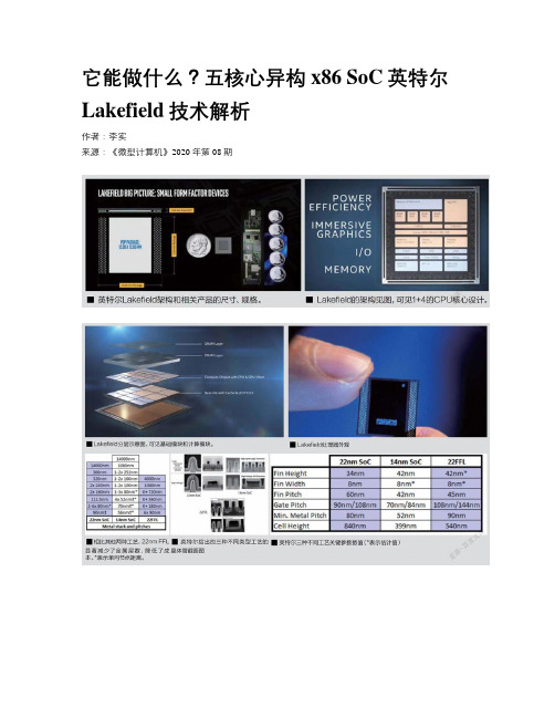
它能做什么?五核心异构x86 SoC英特尔Lakefield技术解析作者:***来源:《微型计算机》2020年第08期在这个智能移动设备已经占据了我们生活绝大部分的年代,如何设计一颗更好、更节能、更适合移动设备使用的处理器,一直以来都是芯片厂商最为关注的话题之一。
在ARM架构中,ARM推出了诸如big.LITTLE以及现在被称作DynamIQ大小核匹配的一整套软硬件解决方案,并带来了非常不错的使用效果。
在x86架构这边,截至目前依旧是大核心对大核心、小核心对小核心,还没有一款产品能够融合两者的优势。
不过,在x86上的这个空白可能要被英特尔填补了。
2019年,英特尔就宣布了新的Atom、Core架构以及全新的Foveros 3D封装技术,以及这些技术综合而来的全新Lakefield处理器和其代表的全新混合式异构架构。
随着Lakefield处理器的消息不断爆出,各种有关这款产品在设计和性能方面的数据开始走向前台,引发了人们对采用这款全新设计、全新架构和独特异构方案的处理器的好奇。
今天,本文就综合多方内容,对这款英特尔未来的移动处理器之星进行解读。
去年,英特尔发布了Lakefield架构。
当時和Lakefield-起登场的还有全新的3D封装技术Foveros以及一些全新的处理器架构设计。
作为英特尔近十年来改变最大的处理器产品,Lakefield在设计思路和实现方式上给人们带来了全新的思考,这款堪称里程碑式的产品,一定会在整个处理器的发展历史中留下浓墨重彩的一笔。
先来看名称,Lakefield是一款移动SoC的代号,也是这款SoC架构特征的名称。
设计方面,全新的Lakefield带来了大量不同于之前处理器的设计,包括更小的电路板尺寸、更出色的功耗和性能功耗比表现等。
架构方面,Lakefield最值得关注的地方还是其独特的异构多核架构,这个架构包含了非偶数的处理器数量,分别是一个大核心和四个小核心,显然,Lakefield 吸取了目前智能手机移动SoC的部分思想,并结合x86实际应用场景的特性。
EN 300400

N e w p r e s e n t a t i o n - s e e H i s t o r y b ox I NTERIM E UROPEAN I-ETS 300 400T ELECOMMUNICATION March 1995S TANDARDSource: ETSI TC-TEReference: DI/TE-04115ICS:33.080Key words:ISDN, telephony, payphone Integrated Services Digital Network (ISDN);Telephony terminals;PayphonesETSIEuropean Telecommunications Standards InstituteETSI SecretariatPostal address: F-06921 Sophia Antipolis CEDEX - FRANCE Office address: 650 Route des Lucioles - Sophia Antipolis - Valbonne - FRANCE X.400: c=fr, a=atlas, p=etsi, s=secretariat - Internet: secretariat@etsi.fr Tel.: +33 92 94 42 00 - Fax: +33 93 65 47 16Copyright Notification: No part may be reproduced except as authorized by written permission. The copyright and the foregoing restriction extend to reproduction in all media.© European Telecommunications Standards Institute 1995. All rights reserved.Page 2I-ETS 300 400: January 1995Whilst every care has been taken in the preparation and publication of this document, errors in content, typographical or otherwise, may occur. If you have comments concerning its accuracy, please write to "ETSI Editing and Committee Support Dept." at the address shown on the title page.Page 3I-ETS 300 400: January 1995ContentsForeword (5)Introduction (5)1Scope (6)2Normative references (7)3Definitions and abbreviations (8)3.1Definitions (8)3.2Abbreviations (8)4Network access (8)4.1General (8)4.2Designation (9)4.3Emergency calls (9)5Telephony functions (9)5.1General (9)5.2Suppression of transmission (9)5.3Inductive coupling (9)6Message functions (9)6.1General (9)6.2Provision of messages (9)6.3Message content (10)6.3.1General (10)6.3.2Language (10)6.4Audio messages (10)6.4.1Speech messages (10)6.4.2Tones (10)7Keypad functions (10)7.1Network addressing (10)7.2Interworking with payment card (10)8Payment methods (11)8.1General (11)8.2Coins/Tokens (11)8.2.1Repayment (11)8.2.2Expiry of credit (11)8.3Prepayment cards (11)8.3.1Return of card (11)8.3.2Expiry of credit (11)8.4Credit and charge cards (11)8.4.1Magnetic stripe card interface (11)8.4.2Return of card (11)8.5IC cards (12)8.5.1General (12)8.5.2Return of card (12)8.5.3Electronic signals and transmission protocols (12)9Power fail requirements (12)9.1Emergency calls (12)9.1.1Designated terminal (12)9.1.2Other terminals (12)Page 4I-ETS 300 400: January 19959.2Payment retention (12)Annex A (normative):Test specifications (13)A.1General conditions for testing (13)A.1.1Test environment (13)A.1.2Test equipment interface (13)A.1.3Test equipment requirements (13)A.1.4Alternative test methods (13)A.1.5Audio message level (13)A.1.5.1Speech messages (13)A.1.5.2Tones (13)A.1.6Return of coins or tokens (13)A.1.7Return of prepayment card (14)A.1.8Return of credit card (14)A.1.9Return of IC card (14)Annex B (informative):Payphone facilities (15)B.1Application recognition (15)B.2Authentication (15)B.3Card Holder Verification (15)B.4Charge card calling (15)B.5Cost optimization (15)B.6Cost of service calculation (16)B.7Data transmission, card/host (16)B.8Dialling - fixed addresses (16)B.9Dialling - last number repeat (16)B.10Dialling - prefix conversion (16)B.11Dialling - short code (16)B.12Remote key pad (17)B.12.1Encrypting key pad (17)B.12.2PIN-pad identification (17)B.13Language recognition (17)B.14Unblocking key - terminal support (17)B.15Validity check - black list (17)B.16Validity check - white list (17)B.17Voice encryption (17)Annex C (informative):Bibliography (18)History (19)Page 5I-ETS 300 400: January 1995 ForewordThis Interim European Telecommunication Standard (I-ETS) was produced by the Terminal Equipment Technical Committee (TC-TE) of the European Telecommunications Standards Institute (ETSI).An ETSI standard may be given I-ETS status as it is regarded either as a provisional solution ahead of a more advanced standard, or because it is immature and requires a "trial period". The life of an I-ETS is limited, at first, to three years after which it can be converted into an European Telecommunication Standard (ETS), have its life extended for a further two years, be replaced by a new version of the I-ETS or be withdrawn.This I-ETS describes the required technical characteristics of Integrated Services Digital Network (ISDN) 3,1 kHz payphone terminals as described in clause 1 (Scope).Terminal equipment may be subject to mandatory standards such as NET 3 (CTR3 in preparation) and CTR 8.IntroductionA payphone service may be provided in a number of ways ranging from a simple self-contained terminal to a complex arrangement of terminal and central processing equipment which interact with one another. A number of methods of payment are possible, ranging from coins or tokens, through to various types of prepayment cards, credit cards and "smart" cards.In general, the complexity of the apparatus required is determined by the facilities offered, the reliability required and the level of assurance that the service provider requires in the validation of the payment.This I-ETS is intended to specify the requirements of that set of functions of a payphone terminal that are necessary to support the range of facilities that may be required in such a variety of terminal apparatus.Some types of payphones may be subject to National or European legislation requiring the mandatory provision of certain facilities. Examples are the provision of inductive coupling or the provision of a printer. This I-ETS does not specify requirements for operation in any particular environments.Page 6I-ETS 300 400: January 1995Blank pagePage 7I-ETS 300 400: January 1995 1ScopeThis I-ETS specifies technical characteristics (electrical, mechanical, logical and acoustic) for a payphone terminal using the 3,1 kHz telephony service which can be connected to an ISDN basic access at the coincident S and T reference point at an interface to a public telecommunications network presented as an ISDN basic access point.The requirements of this I-ETS are additional to those of the standards for connection to the ISDN basic access and of any other standards to which the terminal equipment is subject.This I-ETS is applicable to terminal equipment of the functional group defined as Terminal Equipment Type 1 (TE1) in CCITT Recommendation I.411 which supports the 3,1 kHz telephony teleservice.This I-ETS specifies all the functions necessary to provide real-time two-way speech conversation. Where a function is indicated as optional, it need not be provided, but where such a function is provided, the terminal needs to conform to the requirements and tests specified in this I-ETS.Annex B (informative) contains details of facilities that may be provided on a payphone, whilst the provision of none of these facilities is mandatory, some levels of payphone service cannot be implemented unless certain facilities are present.2Normative referencesThis I-ETS incorporates by dated or undated references, provisions from other publications. These normative references are cited at the appropriate places in the text and the publications are listed hereafter. For dated references, subsequent amendments to or revisions of any of these publications apply to this I-ETS only when incorporated in it by amendment or revision. For undated references the latest edition of the publication referred to applies.[1]I-ETS 300 245-1: "Integrated Services Digital Network (ISDN) - Technicalcharacteristics of telephony terminals - Part 1: General".[2]I-ETS 300 245-2: "Integrated Services Digital Network (ISDN) - Technicalcharacteristics of telephony terminals - Part 2: PCM A-law handset telephony".[3]ETS 300 381: "Telephony for hearing impaired people - Inductive coupling oftelephone earphones to hearing aids, performance requirements and testingmethods".[4]EN 726-4: "Requirements for IC cards and terminals for telecommunication use- Part 4: Application independent card related terminal requirements".[5]ISO 4909 (1987): "Bank cards - Magnetic stripe data content for track 3".[6]ISO 7810 (1985): "Identification cards - Physical characteristics".[7]ISO 7811, Parts 1 to 5 (1985): "Identification cards - Recording technique".[8]ISO 7813 (1990): "Identification cards - Financial transaction cards".[9]prEN 1038: "IC card applications for telecommunications - Part 1 - IC CardPayphone".[10]ETS 300 153: "Integrated Services Digital Network (ISDN) - Attachmentrequirements for terminal equipment to connect to an ISDN using ISDN basicaccess (Candidate NET 3, Part 1)".[11]ITU-T Recommendation P.57 (1993): "Artificial ears".[12]IEC Publication 651: "Sound level meters".Page 8I-ETS 300 400: January 1995[13]CCITT Recommendation P.56 (1988): "Objective measurement of activespeech level".3Definitions and abbreviations3.1DefinitionsFor the purposes of this I-ETS, the following definitions apply, together with the relevant definitions given in I-ETS 300 245-1 [1], I-ETS 300 245-2 [2] and in CCITT Recommendations P.10 and G.701.application: A set of security mechanisms, files, data, protocols (excluding transmission protocols) which are located and used in the Integrated Circuit (IC) card (card application) and outside of the IC card (external application).cardphone: A payphone that accepts cards as a means of payment.charge card: A form of credit card issued by a telecommunications service provider.credit card: A card which permits payment to be made at a date after receiving a service.designated terminal: A terminal that is permitted to draw power from power source 1 under restricted power conditions as specified in CCITT Recommendation I.430.follow-on call: A facility whereby a call may be cleared whilst retaining any payment as credit for a following call.Integrated Circuit Card (IC Card): A card containing a microprocessor, that can be considered as a set of files that can, e.g. be read, written, or executed (sometimes known as a "smart" card).payphone: Terminal apparatus permitting access to the telephony teleservice after the validation of suitable payment. Outgoing calls to certain services may be permitted without payment. Calls to certain services may be barred.payphone service: A service offered by means of special equipment, which permits access to telecommunications services after the validation of suitable payment. The service may be offered by a self-contained terminal or by interaction between a terminal and other apparatus accessed over the network.prepayment card: A card providing payment for a service by means of a stored value paid for in advance.3.2AbbreviationsFor the purposes of this I-ETS, the following abbreviations apply, together with relevant abbreviations given in I-ETS 300 245-1 [1], I-ETS 300 245-2 [2] and CCITT Recommendations P.10 and G.701.CHV Card Holder VerificationCTR Common Technical RegulationIC Integrated CircuitISDN Integrated Services Digital NetworkLRGP Loudness Rating Guard-ring PositionNET Norme Européene de TélécommunicationsPCM Pulse Code ModulationRLR Receive Loudness RatingTE1Terminal Equipment Type 1TEUT Terminal Equipment Under Test4Network access4.1GeneralThe terminal shall comply with I-ETS 300 245-1 [1].Page 9I-ETS 300 400: January 19954.2DesignationA payphone shall be capable of being a designated terminal. As an option, a switching function may be provided to remove the designation.Compliance shall be checked by inspection.4.3Emergency callsThe terminal shall permit calls to the public emergency services without the necessity for payment to be proffered.Compliance shall be checked by attempting a call to the appropriate number(s) without proffering payment.5Telephony functions5.1GeneralThe telephony functions of the terminal shall comply with I-ETS 300 245-1 [1] and I-ETS 300 245-2 [2]. 5.2Suppression of transmissionWhen it is intended to suppress speech transmission (e.g. before validation of payment or after expiry of credit), the sending sensitivity/frequency response should be attenuated by at least 60 dB.Compliance may be checked by a selective measurement of the sending sensitivity/frequency response using the test method specified for sending sensitivity/frequency response specified in I-ETS 300 245-2 [2].5.3Inductive couplingAs an option, a facility may be provided to couple inductively the speech signal to a hearing aid.Such coupling, if provided, shall comply with ETS 300 381 [3].NOTE:The provision of such a facility may be mandatory in some countries.6Message functions6.1GeneralMessages of various kinds are generally necessary in a payphone to give guidance and feedback to the user. Such messages may be internally generated in response to a number of possible stimuli. Examples include some internal logical condition or a signal derived from a key or other control device. Messages may also be generated in response to a message received from an IC card, a message from the network received over the D-channel, or a message from the payphone service provider received over a B- or D-channel.Messages may be presented to the user as an audible signal in the form of a tone or a spoken message, as a visual display in the form of a symbol or as an alpha numeric message, or even in a tactile manner in the form of braille or other language for the visually handicapped.6.2Provision of messagesThe provision of messages is optional. Where a message is provided, it shall be consistent with its stimulus.Compliance shall be checked by inspection.Page 10I-ETS 300 400: January 19956.3Message content6.3.1GeneralIt is preferable that there should be a set of basic messages associated as necessary with specified signals received by the payphone, from, for example, the network or an IC card.It should be possible to suppress the display of user related data.Typical messages may include, for example:-insert payment;-insert your card;-remove your card;-enter your number;-try again;-emergency calls only.6.3.2LanguageAt least two languages shall be supported, one of which should be English. Means of language selection are described in EN 726-4 [4].6.4Audio messages6.4.1Speech messagesSpeech messages originated by the payphone shall be presented at a level of - 14 dBPa ± 6 dB long term rms while active when the Receive Loudness Rating (RLR) is at the nominal value.Compliance shall be checked by the test described in annex A, subclause A.1.5.6.4.2TonesTones originated by the payphone shall be presented at a level of - 5 dBPa ± 4 dBPa when the Receive Loudness Rating (RLR) is at the nominal value.Compliance shall be checked by the test described in annex A, subclause A.1.5.7Keypad functions7.1Network addressingAny control information transmitted over the D-channel as a result of a key operation shall be consistent with the marking on the key.Compliance shall be checked by inspection.7.2Interworking with payment cardAny signal appearing at a payment card interface as a result of a key operation shall be consistent with the marking on the key.Compliance shall be checked by inspection.8Payment methods8.1GeneralA payphone shall support at least one method of payment. Payment methods are optional (e.g. coins, tokens, coded cards), and the validity of such payment may be verified by any means acceptable to the payphone service provider.8.2Coins/Tokens8.2.1RepaymentPayphones which provide a coin/token operated prepayment facility shall return any coins/tokens proffered which have not been used as payment for the call upon call clearing initiated by the payphone, unless a follow-on call facility has been activated.Compliance shall be checked by the test described in annex A, subclause A.1.6.8.2.2Expiry of creditA warning shall be given to the user before the expiry of any credit.Compliance shall be checked by inspection.8.3Prepayment cards8.3.1Return of cardAny card with credit remaining shall be returned to the user at the end of a call unless a follow-on call facility has been activated.Compliance shall be checked by the test described in annex A, subclause A.1.7.NOTE: A means of alerting should be provided to warn the user to retrieve the card.8.3.2Expiry of creditA warning shall be given to the user before the expiry of any credit on the card.Compliance shall be checked by inspection.8.4Credit and charge cards8.4.1Magnetic stripe card interfaceFor a payphone that accepts magnetic stripe credit and charge cards, the card/payphone interface shall be compatible with the characteristics specified in ISO 4909 [5], ISO 7810 [6], ISO 7811 [7] and ISO 7813 [8] as applicable.8.4.2Return of cardThe card shall be returned to the user, at the latest when the call is cleared by the payphone unless a follow-on call facility has been activated.Compliance shall be checked by the test described in annex A, subclause A.1.8.NOTE: A means of alerting should be provided to warn the user to retrieve the card.8.5IC cards8.5.1GeneralA payphone that accepts IC cards shall meet the requirements of prEN 1038 [9].8.5.2Return of cardThe card shall be returned to the user, at the latest when the call is cleared by the payphone unless a follow-on call facility has been activated.Compliance shall be checked by the test described in annex A, subclause A.1.9.NOTE: A means of alerting should be provided to warn the user to retrieve the card.8.5.3Electronic signals and transmission protocolsA payphone that accepts IC cards shall meet the requirements for the electronic signals and the asynchronous/synchronous transmission protocols across the card/payphone interface that are described in clause 5 of EN 726-4 [4].9Power fail requirements9.1Emergency calls9.1.1Designated terminalA designated terminal shall under all conditions be capable of providing as a minimum the functions necessary to support telephony 3,1 kHz teleservice, a real-time 2-way speech conversation and calls to the emergency services without the need to proffer payment.Compliance shall be checked by placing the terminal under restricted power conditions, by removing all sources of local power and attempting a call to an emergency service number.9.1.2Other terminalsA payphone that is not a designated terminal shall automatically give a "not available" indication when unable to make calls.Compliance shall be checked by removing all sources of local power (including power source 1).9.2Payment retentionThe payphone shall not falsely retain payment due to any power failure.Compliance shall be checked by removing all sources of local power (including power source 1).Annex A (normative):Test specificationsA.1General conditions for testingA.1.1Test environmentThe test environment is described in ETS 300 153 [10], clause 4.A.1.2Test equipment interfaceThe interface on the test equipment connected to the terminal under test shall be capable of providing the signalling and supervision necessary for the terminal to be working in all test modes. The connection of the test equipment to the terminal under test at the coincident S and T reference point shall be in accordance with ETS 300 153 [10], clause 4.A.1.3Test equipment requirementsartificial ear: The default artificial ear is the ITU-T Recommendation P.57 [11] type 1 artificial ear.When measuring low acoustic impedance receivers the ITU-T Recommendation P.57 [11], type 3.2 artificial ear shall be used. The low leakage option shall be adopted. Sound pressure measurements shall be referred to the Ear Reference Point (ERP) by the correction characteristic specified in ITU-T Recommendation P.57 [11].sound level meter: The sound level measurement equipment shall conform to IEC Publication 651 [12], type 1. The "I" detector characteristic shall be used.speech voltmeter: The speech voltmeter shall conform to CCITT Recommendation P.56 [13].A.1.4Alternative test methodsThe requirements of this I-ETS were written on the basis of the standard test methods described in this annex. For some parameters, it is recognised that alternative test methods may exist. It shall be the responsibility of the test house to ensure that any alternative method used is equivalent to that described in this annex.A.1.5Audio message levelA.1.5.1Speech messagesThe handset is mounted at the Loudness Rating Guard-ring Position (LRGP) and the earpiece is sealed to the knife-edge of the artificial ear.The Terminal Equipment Under Test (TEUT) is caused to generate a message and the speech level in the artificial ear shall be determined using a speech voltmeter using method B of CCITT Recommendation P.56 [13].A.1.5.2TonesThe handset shall be mounted in the Loudness Rating Guard-ring Position (LRGP) and the ear piece shall be sealed to the knife-edge of an artificial ear.The sound pressure shall be measured by connecting the sound level meter to the artificial ear.A.1.6Return of coins or tokensA call shall be set up using suitable coins or tokens as means of payment, and the call shall be cleared down whilst coins or tokens remain unused.Unused coins or tokens shall be returned to the user.A.1.7Return of prepayment cardA call shall be set up using a suitable prepayment card as means of payment, and the call shall be cleared down before the credit on the card is fully used.The card shall be returned to the user.A.1.8Return of credit cardA call shall be set up using a suitable credit card as means of payment, and the call shall be cleared down.The card shall have been returned to the user by the completion of this operation.A.1.9Return of IC cardA call shall be set up using a suitable IC card as means of payment, and the call shall be cleared down. The card shall have been returned to the user by the completion of this operation.Annex B (informative):Payphone facilitiesThis annex contains descriptions of some possible payphone facilities that can be provided using the functions specified in the body of this I-ETS.Whilst the provision of none of these facilities is mandatory, some levels of payphone service cannot be implemented unless certain facilities are present.In general this will be a matter for agreement between the supplier and the payphone service provider, but the provision of certain facilities in regulated payphones may be subject to legislation.B.1Application recognitionA facility whereby the terminal reads an IC card and determines whether it can support the application(s) resident on the card, so that it can then proceed according to the rules defined for that application.If the application that is desired cannot be supported, the card is returned to the user and an appropriate message is displayed.The provision of such a facility would typically involve the keypad functions (clause 7), the IC card function (subclause 8.5) and the message functions (clause 6).B.2AuthenticationIf two parties wish to communicate, then each party may wish to satisfy itself that the other is genuine. In the case of an IC card, the two parties are the card and the outside world, which includes everything outside the card.The process of authentication may therefore typically involve the keypad function (clause 7), the message functions (clause 6) and the electronic signal and transmission protocols of the IC card (subclause 8.5.3).B.3Card Holder VerificationCard Holder Verification (CHV) enables the user to prove identity by entering a Cardholder Verification code and/or by the input of biometric information.In the case of a CHV entry, the keypad/keyboard of the terminal or a separate and secure PIN-pad may be used.The provision of such a facility would typically involve the keypad functions (clause 7), the IC card function (subclause 8.5), possibly the network access function (subclause 4.1) and possibly a biometric reader function (unspecified).B.4Charge card callingA facility which allows a user to make a call from a cardphone and have the charges for the call automatically charged to a service subscriber's account number as defined by information contained on the card.Such a service utilises procedures defined in CCITT/ITU-T Recommendations E.116, and E.118 and ITU-T Recommendation E.113.The provision of such a facility would typically involve the keypad functions (clause 7), the credit card function (subclause 8.4), the IC card function (subclause 8.5) and the network access function (subclause4.1).B.5Cost optimizationThis facility would allow the terminal to determine the least cost communication route using information resident on an IC card.Provision of this facility would typically involve the network access function (subclause 4.1), the keypad functions (clause 7) and the electronic signals and transmission protocols of the IC card (subclause 8.5.3).B.6Cost of service calculationA facility whereby the terminal calculates and displays the cost of providing the chosen service or the cost of a call using information derived from the network or from its own internal intelligence.Such a facility may make use of the ISDN supplementary service of Advice of Charge (ETS 300 178, ETS 300 179, ETS 300 180, ETS 300 181).Provision of this facility would typically involve the network access function (subclause 4.1), the keypad functions (clause 7) and the message functions (clause 6).B.7Data transmission, card/hostThis is a facility whereby an IC card can communicate directly with a host computer, e.g. to receive a new application or to update an existing one. This dialogue could be carried on whilst the user is using some other service provided by the terminal.Signalling could be over any available channel and might involve use of the user signalling bearer service defined in ITU-T Recommendation I.232.3.Provision of this facility would typically involve the network access function (subclause 4.1), and the electronic and signals transmission protocols (subclause 8.5.3).B.8Dialling - fixed addressesThis facility automatically dials a number determined by the card application selected by the user. For an IC card, this should be in accordance with prEN726-6.Provision of this facility would typically involve the network access function (subclause 4.1), the keypad function (clause 7), and the electronic signal and transmission protocols of the IC card (subclause 8.5.3).B.9Dialling - last number repeatA facility whereby the last number dialled to access the network may be stored automatically. Where the number is stored within an IC card in accordance with prEN726-6, the number may then subsequently be redialled from the terminal or from another IC card terminal.Provision of this facility would typically involve the network access function (subclause 4.1), the keypad function (clause 7), and the electronic signal and transmission protocols of the IC card (subclause 8.5.3).B.10Dialling - prefix conversionA facility whereby when an IC card of one nationality is inserted into a terminal of a second nationality, and a telephone number is selected from a directory on the card, the appropriate national prefixes are inserted into the dialled number in accordance with prEN726-6.Provision of this facility would typically involve the network access function (subclause 4.1), the keypad function (clause 7), and the electronic signal and transmission protocols of the IC card (subclause 8.5.3).B.11Dialling - short codeA facility whereby a long number stored on an IC card may be dialled by dialling a shorter directory code. The terminal is expected to generate the correct prefixes dependent on the country, area and network accessed.Provision of this facility would typically involve the network access function (subclause 4.1), the keypad function (clause 7) and the electronic signal and transmission protocols of the IC card (subclause 8.5.3).。
fips-197

7. Specifications. Federal Information Processing Standard (FIPS) 197, Advanced Encryption Standard (AES) (affixed). 8. Implementations. The algorithm specified in this standard may be implemented in software, firmware, hardware, or any combination theion may depend on several factors such as the application, the environment, the technology used, etc. The algorithm shall be used in conjunction with a FIPS approved or NIST recommended mode of operation. Object Identifiers (OIDs) and any associated parameters for AES used in these modes are available at the Computer Security Objects Register (CSOR), located at /csor/ [2]. Implementations of the algorithm that are tested by an accredited laboratory and validated will be considered as complying with this standard. Since cryptographic security depends on many factors besides the correct implementation of an encryption algorithm, Federal Government employees, and others, should also refer to NIST Special Publication 800-21, Guideline for Implementing Cryptography in the Federal Government, for additional information and guidance (NIST SP 800-21 is available at /publications/). 9. Implementation Schedule. This standard becomes effective on May 26, 2002. 10. Patents. Implementations of the algorithm specified in this standard may be covered by U.S. and foreign patents. 11. Export Control. Certain cryptographic devices and technical data regarding them are subject to Federal export controls. Exports of cryptographic modules implementing this standard and technical data regarding them must comply with these Federal regulations and be licensed by the Bureau of Export Administration of the U.S. Department of Commerce. Applicable Federal government export controls are specified in Title 15, Code of Federal Regulations (CFR) Part 740.17; Title 15, CFR Part 742; and Title 15, CFR Part 774, Category 5, Part 2. 12. Qualifications. NIST will continue to follow developments in the analysis of the AES algorithm. As with its other cryptographic algorithm standards, NIST will formally reevaluate this standard every five years. Both this standard and possible threats reducing the security provided through the use of this standard will undergo review by NIST as appropriate, taking into account newly available analysis and technology. In addition, the awareness of any breakthrough in technology or any mathematical weakness of the algorithm will cause NIST to reevaluate this standard and provide necessary revisions. 13. Waiver Procedure. Under certain exceptional circumstances, the heads of Federal agencies, or their delegates, may approve waivers to Federal Information Processing Standards (FIPS). The heads of such agencies may redelegate such authority only to a senior official designated pursuant to Section 3506(b) of Title 44, U.S. Code. Waivers shall be granted only when compliance with this standard would a. adversely affect the accomplishment of the mission of an operator of Federal computer system or b. cause a major adverse financial impact on the operator that is not offset by governmentwide savings.
7_JVM_intro

ClassFile { u4 magic; Number of u2 minor_version; fields, each u2 major_version; u2 constant_pool_count; field_info item cp_info constant_pool[constant_pool_count-1]; provides u2 access_flags; u2 this_class; complete u2 super_class; information u2 interfaces_count; u2 interfaces[interfaces_count]; about a field
A java class file is defined as a stream of 8bit bytes consisting of a single ClassFile structure (where the structure is as in the C programming language): Tools will take care of most of the details of constructing a classfile, but it is useful to understand the overall structure.
Java Virtual Machine
Java compilers start with Java source code and create class files containing Java byte code When a Java program is executed, the byte code in the class file is
一种英特尔Hex文件的解析和填充方法
4 Hex 文件解析的实现
图 1 中展示的 Hex 文件内容,PROM 从地址 0x8001000 至 0x803FFFFF,共计 4032Kbytes。 文件以 Record Type 0x04 为起始,以 Record Type 0x01 为结束,中间行穿插着 Record Type 0x04,分别记录了不同的 linear Address,如果上一个 Record 的结束地址与当前 Record 的起始地址不连续,则视 为 Block 中断。
容位于 MCU PROM 中的哪个位置; ● Record 的类型,表示第 5 个域中所含内容的意义,所
含的是一个基地址或数据; ● Record 的校验和,表示这个 Record 中所含数据的校
验和。
● RecordType 0x00,表示域 5 中的内容是数据。 ● RecordType 0x01,表示这是整个 hex 文件中最后一个 record。 ● RecordType 0x02,可同时用于 16 位和 32 位格式的 MCU,表示 16 位地址中的高 12 位,低 4 位是 0。 ● RecordType 0x03,可同时用于 16 位和 32 位格式的 MCU,是专门针对 8086 和 80186 这种架构的 MCU,DATA 中定义的 4 字节数据是 CS 和 IP 寄存器中的值。 ● RecordType 0x04,仅针对 32 位格式的 MCU,表示的 是 32 位地址的高 16 位基地址,低 16 位是 0x0000。 ● RecordType 0x05,这种 record type 仅针对 32 位格式 的 MCU,表示的是这个 hex 文件内容的起始执行地址。 根据 Record Type 对 Hex 文件中的每个 Record 进行相应 意义的解析,从而梳理出 Hex 文件的起始执行地址,每个 Block 的起始地址和长度。
PCLint使用指南
更多参考资料下载:
第一讲 PCLint/FlexeLint 介绍
1.1 介绍
该软件在 PC 市场(Windows,MS-DOS, OS/2) 就叫做 PCLint,对于其他平台, 则称作 FlexeLint。这就是 PCLint/FlexeLint 的来历。本文只考虑 PCLint/FlexeLint 在 Windows 下的使用,因此下面使用的 PCLint 就是指 PCLint/FlexeLint。
[MISRA Rule 13] demo.c(1) : Note 971: Use of 'char' without 'signed' or 'unsigned' [MISRA Rule
14] _ { demo.c(2) : Note 957: Function 'report' defined without a prototype in scope
1
更多参考资料下载:
版权声明
技术是人类共同的财富,同时本文选取的数值计算程序库都来源开源社区, 没有秘密可言。再说开源的初衷就是为了共享、传播知识。因此,作者愿意公开 本电子文档,并乐于与大家分享我的学习成果。
版权声明如下: (1)读者可以任意拷贝、修改本书的内容,但不可以篡改作者及所属单位。 (2)未经作者许可,不得公开出版或大量印发以获取利益,以传播知识为 目的电子拷贝除外。 (3)请遵守其他法律规定,以免发生纠纷。 欢迎读者对本文档提出批评建议,信息反馈请联系 Email:openlek@。
[6] Meyers, Scott,Effective C++,Addison-Wesley, Reading MA, 1992 [7] Cargill, Tom,C++ Gotchas,presented at C++ World, November 1992.
嵌入式开发工具发展趋势-李宁

软件仿真技术——软件仿真的优点 ★ 加快软件开发进度 ★ 降低硬件调试成本 ★ 降低学习入门门槛
软件仿真技术——至下而上,全面的软件仿真
★ CPLD/FPGA设计的仿真 ★ 系统设计的仿真
★ 单元模块设计的仿真
FPGA/CPLD仿真——Quartus II
单元模块仿真——RealView MDK
MCU发展对工具的挑战——4/8/16到32位的无缝转变
■ 能否帮工程师实现这种无缝转变? ■ 工程师所熟悉界面和接口的工具 ■ RealView MDK支持ARM7、ARM9和 ARM Cortex-M3,提供4/8/16处理器开 发常用的µVision3 IDE环境,简单易 用,可以帮助工程师很快地上手。
How to change into
4/8/16 -bit
32-bit
MCU发展对工具的挑战——如何加快开发周期?
中型软件项目,77.5%可完成,25.5%不能如期完成 大型软件项目,13.5%可完成,61.8%被取消 嵌入式开发,需要软、硬件工程师紧密配合协同工作
如何加快开发周期? 能否脱离硬件,先进行软件调试?
基于Cortex-M3的产品: Luminary Micro公司 的Stellaris系列 ST公司的STM32系列 ……
MCU发展对工具的挑战——工程师需要什么工具?
Which one should I choose?
Keil
RVDS、MDK
Workbench
CodeWarrior
MULTI MPLAB Xilinx Platform Studio IAR EWARM Dynamic C VisualDSP++ Nios II IDE
中型项目 大型项目
移动开发培训有哪些课程
1、IONICIONIC是目前十分有潜力的一款HTML5手机应用开发框架。
通过SASS构建应用程序,它提供了很多UI组件来帮助使用者开发强大的应用。
它使用JavaScript MVVM框架和AngularJS来增强应用。
提供数据的双向绑定,使用它成为Web和移动使用者的共同选择。
即将发布的AngularJS 2.0将会专注于移动开发,相信IONIC一定会取得不错的成就。
IONIC的开发团队将尽快开发出一种通过IONIC creator提供使用者快速创建IONIC应用的方式。
我们将很快就会看到一个支持拖拉功能的可视化开发工具,几分钟内开发一个app将成为可能。
2、Mobile Angular UIMobile Angular UI是使用bootstrap 3和AngularJS的响应式移动开发HTML5框架。
Mobile Angular UI的关键字有:Bootstrap 3、AngularJS。
Bootstrap 3 Mobile组件,比如switches, overlays和sidebars,这些都是bootstrap中没有的。
AngularJS modules,比如angular-route, angular-touch 和angular-animate响应式媒体查询是将bootstrap作为单独的文件,你只需要包含你所需要的东西。
Mobile Angular UIu并不包含任何jQuery依赖,你需要做的只是通过一些AngularJS指令创建友好的用户体验。
详细了解可以看一看the Mobile Angular UI demo page,上面有Mobile Angular UI的实践,如果你想了解的更深入一些,我建议你读一读getting started with Mobile Angular UI。
3、Intel XDKIntel XDK 是Inter开发的一款跨平台开发工具,我们可以很容易的通过Intel XDK开发应用,你需要做的只是下载他们的应用开发工具,有Linux、Windows和Mac版,它还提供了很多个开发框架,比如Twitter bootstrap,jQuery Mobile和Topcoat。
RK音频简介以及常见问题debug方法v1.1
以 es8323 为例调试新的驱动 .................................................................................................................. 25
蓝牙通话 3G 通话的方案 DEBUG ............................................................................................................... 30 312X 平台 CODEC DEBUG .......................................................................................................................... 30 POP 音问题 ................................................................................................................................................... 30 关于 ALC 功能 ................................................................................................................................................. 31 关于降噪算法 ................................................................................................................................................... 31 ALSA 的上层应用程序 ................................................................................................................................... 32
HTML5新特性详解
HTML5新特性详解HTML5是HyperText Markup Language(超文本标记语言)的第五个版本,于2014年10月由万维网联盟(W3C)发布。
它为Web开发带来了许多新特性,可以帮助开发人员更有效地创建功能更强大的网站。
1. 语义元素HTML5引入了许多新的语义元素,可以更准确地描述页面内容和结构。
一些示例包括:header(页面或部分的标题)、nav (导航条)、section(文档中的一个独立部分)和 article(独立的可复用内容)。
使用这些元素可以更容易地理解页面结构,从而实现更好的可访问性和SEO。
2. 支持视频和音频HTML5允许使用 video 和 audio 元素来嵌入可播放的视频和音频。
这可以减少对第三方插件如Flash的依赖,并可以更好地控制媒体播放体验。
另外,通过 WebVTT(Web视频文本轨道)标准,可以添加字幕和注释,从而提高可访问性。
3. Canvas绘图HTML5中的 Canvas 元素允许使用JavaScript创建动态图形和动画效果。
可以使用 Canvas 实现流畅的动画以及绘制矢量和光栅图像。
Canvas也有许多用途,如数据可视化、游戏开发和交互式图表等。
4. 本地存储HTML5允许使用本地存储,也称为Web存储,以将数据存储在客户端浏览器中。
此外,HTML5还允许使用IndexedDB API来支持更复杂的本地存储。
这为离线应用程序提供了极大的优势,因为应用程序可以缓存数据以供以后使用,而不必再次从服务器获取数据。
5. 地理位置APIHTML5可以使用地理定位API,该API可让网站请求用户的地理位置信息。
这可以用于许多用途,如体育活动跟踪、商业定位和天气预报等。
这种功能可能会显著影响用户隐私和安全,用户应该知道何时和如何共享其位置信息。
6. Web Workers和Web SocketsHTML5支持 Web Workers 和 Web Sockets 两种新技术,可以将大量数据异步处理和实时通信。
博通BCM43362-wifi 资料

Single-Chip IEEE 802.11™ b/g/n MAC/Baseband/Radio + SDIO Figure 1: BCM43362 System Block Diagram GENERAL DESCRIPTIONFEATURES The Broadcom® BCM43362 single-chip device provides the highest level of integration for mobileand handheld wireless systems, featuring integrated IEEE 802.11™ b/g and handheld device class IEEE 802.11n. It includes a 2.4 GHz WLAN CMOS power amplifier (PA) that meets the output power requirements of most handheld systems. An optional external low-noise amplifier (LNA) and external PA are also supported.Along with the integrated power amplifier, the BCM43362 also includes integrated transmit and receive baluns, further reducing the overall solution cost.Host interface options include SDIO v2.0 that can operate in 4b or 1b modes, and a generic gSPI mode.Utilizing advanced design techniques and process technology to reduce active and idle power, the BCM43362 is designed to address the needs of highly mobile devices that require minimal power consumption and compact size. It includes a power management unit that simplifies the system power topology and allows for operation directly from a rechargeable mobile platform battery while maximizing battery life.•Single-band 2.4 GHz IEEE 802.11 b/g/n •Integrated WLAN CMOS power amplifier with internal power detector and closed-loop power control •Internal fractional-N PLL enables the use of a wide range of reference clock frequencies •Supports IEEE 802.15.2 external 3-wire and 4-wire coexistence schemes to optimize bandwidth utilization with other co-located wireless technologies such as Bluetooth, GPS, WiMax, or UWB. •Supports standard interfaces SDIO v2.0 (50 MHz, 4-bit and 1-bit) and generic SPI (up to 50 MHz)•Integrated ARM Cortex™-M3 CPU with on-chip memory enables running IEEE 802.11 firmwarethat can be field-upgraded with future features.•Supports WMM®, WMM-PS, and Wi-Fi Voice Personal (upgradable to Voice Enterprise in the future)•Security:–Hardware WAPI acceleration engine –AES and TKIP in hardware for faster data encryption and IEEE 802.11i compatibility –WPA™- and WPA2™- (Personal) support for powerful encryption and authentication •Programmable dynamic power management•Supports battery voltage range from 2.3V to 5.5V supplies with internal switching regulator• 1 kbit One-Time Programmable (OTP) memory for storing board parameters •69-bump WLBGA (4.52 mm x 2.92 mm, 0.4 mm pitch)Broadcom®, the pulse logo, Connecting everything®, and the Connecting everything logo are among the trademarks of Broadcom Corporation and/or its affiliates in the United States, certain other countries and/or the EU. Any other trademarks or trade names mentioned are the property of their respective owners.This data sheet (including, without limitation, the Broadcom component(s) identified herein) is not designed, intended, or certified for use in any military, nuclear, medical, mass transportation, aviation, navigations, pollution control, hazardous substances management, or other high-risk application. BROADCOM PROVIDES THIS DATA SHEET “AS-IS,” WITHOUT WARRANTY OF ANY KIND. BROADCOM DISCLAIMS ALL WARRANTIES, EXPRESSED AND IMPLIED, INCLUDING, WITHOUT LIMITATION, THE IMPLIED WARRANTIES OF Broadcom Corporation 5300 California Avenue Irvine, CA 92617© 2011 by Broadcom Corporation All rights reserved Printed in the U.S.A.Revision History Revision Date Change Description 43362-DS101-R 02/17/11Updated:•LPO clock to LPO sleep clock throughout the document.•Figure 3: “Power Topology,” on page 13.•“TCXO” on page 18.•Table 2: “Crystal Oscillator and External Clock Requirements and Performance,” on page 19.•“External 32.768 kHz Low-Power Oscillator” on page 20.•Table 3: “External 32.768 kHz Low-Power Oscillator Specifications,” on page 20.•Table 6: “gSPI Registers,” on page 29.•Table 8: “WLBGA Signal Descriptions,” on page 47.•Table 9: “BCM43362 During Reset and After Reset or During Sleep,” on page 53.•Table 12: “Environmental Ratings,” on page 57.•Table 13: “ESD Specifications,” on page 57.•Table 14: “Recommended Operating Conditions and DC Characteristics,” on page 58.•Table 16: “WLAN 2.4 GHz Receiver Performance Specifications,” on page 60.•Table 17: “WLAN 2.4 GHz Transmitter Performance Specifications,” on page 63.•Table 18: “General Spurious Emissions Specifications,” on page 65.•Table 19: “Core Buck Regulator,” on page 66.•Table 20: “3.3V LDO (LDO3P3),” on page 69.•Table 21: “CLDO,” on page 70.•Table 22: “LNLDO1,” on page 71.•“gSPI Signal Timing” on page 76.43362-DS100-R 07/15/10Initial releaseTable of ContentsAbout This Document (8)Purpose and Audience (8)Acronyms and Abbreviations (8)Document Conventions (8)References (9)Technical Support (9)Section 1: BCM43362 Overview (10)Overview (10)Standards Compliance (11)Section 2: Power Supplies and Power Management (12)WLAN Power Management (12)Power Supply Topology (13)Voltage Regulators (14)PMU Sequencing (14)Low-Power Shutdown (15)CBUCK Regulator Features (15)Section 3: Frequency References (17)Crystal Interface and Clock Generation (17)TCXO (18)External 32.768 kHz Low-Power Oscillator (20)Section 4: WLAN System Interfaces (21)SDIO v2.0 (21)SDIO Pin Descriptions (21)Generic SPI Mode (23)SPI Protocol (23)Command Structure (26)Write (26)Write/Read (26)Read (26)Status (27)gSPI Host-Device Handshake (29)Boot-Up Sequence (29)External Coexistence Interface (32)Section 5: Wireless LAN MAC and PHY (33)MAC Features (33)MAC Description (33)PSM (34)WEP (35)TXE (35)RXE (35)IFS (36)TSF (36)NAV (36)MAC-PHY Interface (36)PHY Description (37)PHY Features (37)Section 6: WLAN Radio Subsystem (40)Receive Path (41)Transmit Path (41)Calibration (41)Section 7: CPU and Global Functions (42)WLAN CPU and Memory Subsystem (42)One-Time Programmable Memory (42)GPIO Interface (43)JTAG Interface (43)UART Interface (43)Section 8: WLAN Software Architecture (44)Host Software Architecture (44)Device Software Architecture (44)Remote Downloader (45)Wireless Configuration Utility (45)Section 9: Pinout and Signal Descriptions (46)Signal Assignments (46)WLAN GPIO Signals and Strapping Options (55)Section 10: DC Characteristics (56)Absolute Maximum Ratings (56)Environmental Ratings (57)Electrostatic Discharge Specifications (57)Recommended Operating Conditions and DC Characteristics (58)Section 11: WLAN RF Specifications (59)2.4 GHz Band General RF Specifications (60)WLAN 2.4 GHz Receiver Performance Specifications (60)WLAN 2.4 GHz Transmitter Performance Specifications (63)General Spurious Emissions Specifications (65)Section 12: Internal Regulator Electrical Specifications (66)Core Buck Regulator (66)3.3V LDO (LDO3P3) (69)CLDO (70)LNLDO1 (71)Section 13: System Power Consumption (72)Section 14: Interface Timing and AC Characteristics (73)SDIO Default Mode Timing (73)SDIO High-Speed Mode Timing (75)gSPI Signal Timing (76)JTAG Timing (77)Section 15: Package Information (78)Package Thermal Characteristics (78)Junction Temperature Estimation and PSI Versus Theta jc (78)Section 16: Mechanical Information (79)Section 17: Ordering Information (80)Figure 1: BCM43362 System Block Diagram (1)Figure 2: BCM43362 Block Diagram (10)Figure 3: Power Topology (13)Figure 4: Recommended Oscillator Configuration (17)Figure 5: Recommended Circuit to Use with an External Dedicated TCXO (18)Figure 6: Recommended Circuit to Use with an External Shared TCXO (18)Figure 7: Signal Connections to SDIO Host (SD 4-Bit Mode) (21)Figure 8: Signal Connections to SDIO Host (SD 1-Bit Mode) (22)Figure 9: Signal Connections to SDIO Host (gSPI Mode) (23)Figure 10: gSPI Write Protocol (24)Figure 11: gSPI Read Protocol (25)Figure 12: gSPI Command Structure (26)Figure 13: gSPI Signal Timing Without Status (27)Figure 14: gSPI Signal Timing with Status (Response Delay = 0) (28)Figure 15: WLAN Boot-Up Sequence (31)Figure 16: 4-Wire Coexistence Wiring (32)Figure 17: WLAN MAC Architecture (34)Figure 18: WLAN PHY Block Diagram (38)Figure 19: STBC Receive Block Diagram (39)Figure 20: Radio Functional Block Diagram (40)Figure 21: WLAN Software Architecture (45)Figure 22: 69-Ball WLBGA Ball Map (46)Figure 23: RF Port Location (59)Figure 24: CBUCK Efficiency (68)Figure 25: SDIO Bus Timing (Default Mode) (73)Figure 26: SDIO Bus Timing (High-Speed Mode) (75)Figure 27: gSPI Timing (76)Figure 28: 69-Ball WLBGA Mechanical Information (79)Table 1: CBUCK Operating Mode Selection (16)Table 2: Crystal Oscillator and External Clock Requirements and Performance (19)Table 3: External 32.768 kHz Low-Power Oscillator Specifications (20)Table 4: SDIO Pin Descriptions (21)Table 5: gSPI Status Field Details (28)Table 6: gSPI Registers (29)Table 7: Coexistence Signals (32)Table 8: WLBGA Signal Descriptions (47)Table 9: BCM43362 During Reset and After Reset or During Sleep (53)Table 10: GPIO Functions and Strapping Options (55)Table 11: Absolute Maximum Ratings (56)Table 12: Environmental Ratings (57)Table 13: ESD Specifications (57)Table 14: Recommended Operating Conditions and DC Characteristics (58)Table 15: 2.4 GHz Band General RF Specifications (60)Table 16: WLAN 2.4 GHz Receiver Performance Specifications (60)Table 17: WLAN 2.4 GHz Transmitter Performance Specifications (63)Table 18: General Spurious Emissions Specifications (65)Table 19: Core Buck Regulator (66)Table 20: 3.3V LDO (LDO3P3) (69)Table 21: CLDO (70)Table 22: LNLDO1 (71)Table 23: System Power Consumption (72)Table 24: SDIO Bus Timing Parameters (Default Mode) (74)Table 25: SDIO Bus Timing Parameters (High-Speed Mode) (75)Table 26: gSPI Timing Parameters (76)Table 27: JTAG Timing Characteristics (77)Table 28: Package Thermal Characteristics (78)About This Document BCM43362 Advance Data SheetAbout This DocumentPurpose and AudienceThis document provides engineering design information for the BCM43362, a single chip with an integrated 2.4 GHz RF transceiver, MAC, and baseband processor that fully supports the IEEE 802.11™ b/g/n standards. The information provided is intended for hardware design engineers who will be incorporating the BCM43362 into their designs.Acronyms and AbbreviationsIn most cases, acronyms and abbreviations are defined on first use.For a comprehensive list of acronyms and other terms used in Broadcom documents, go to:/press/glossary.php.Document ConventionsThe following conventions may be used in this document:Convention DescriptionBold User input and actions: for example, type exit, click OK, press Alt+CMonospace Code: #include <iostream>HTML: <td rowspan = 3>Command line commands and parameters: wl [-l] <command>< >Placeholders for required elements: enter your <username> or wl <command>[ ]Indicates optional command-line parameters: wl [-l]Indicates bit and byte ranges (inclusive): [0:3] or [7:0]Technical Support BCM43362 Advance Data Sheet ReferencesThe references in this section may be used in conjunction with this document.For Broadcom documents, replace the “xx” in the document number with the largest number available in the repository to ensure that you have the most current version of the document.Technical SupportBroadcom provides customer access to a wide range of information, including technical documentation, schematic diagrams, product bill of materials, PCB layout information, and software updates through its customer support portal (https:// ). For a CSP account, contact your Sales or Engineering support representative.In addition, Broadcom provides other product support through its Downloads & Support site(/support/).Note: Broadcom provides customer access to technical documentation and software through itsCustomer Support Portal (CSP) and Downloads & Support site (see Technical Support ).Document (or Item) Name Number Source Broadcom Items[1]BCM43362 reference board schematics – Broadcom RepresentativeBCM43362 Advance Data SheetBCM43362 Overview Section 1: BCM43362 Overview OverviewThe Broadcom® BCM43362 provides the highest level of integration for a mobile or handheld wireless system, with integrated IEEE 802.11 b/g/n. It provides a small form-factor solution with minimal external components to drive down cost for mass volumes and allows for handheld device flexibility in size, form, and function. The BCM43362 is designed to address the needs of highly mobile devices that require minimal power consumption and reliable operation.Figure 2 shows the interconnect of all the major physical blocks in the BCM43362 and their associated external interfaces, which are described in greater detail in the following sections.Figure 2: BCM43362 Block DiagramStandards Compliance BCM43362 Advance Data SheetStandards ComplianceThe BCM43362 supports the following standards:•IEEE 802.11n•802.11b•802.11g•802.11d•802.11h•802.11i•802.11jThe BCM43362 will support the following future drafts/standards:•802.11w —S ecure Management Frames•802.11 Extensions:•WMM®•802.11i MAC Enhancements•802.11r Fast Roaming Support (between APs)•802.11k Radio Resource Measurement•Security:•WEP•WAPI•WPA™Personal•WPA2™Personal•AES (Hardware Accelerator)•TKIP (HW Accelerator)•CKIP (SW Support)•QOS Protocols:•WMM•WWM-PS (U-APSD)•WWM-SA•Proprietary Protocols:•CCXv2•CCXv3•CCXv4•CCXv5•WFAEC•Coexistence Interfaces:•Supports IEEE 802.15.2 external three-wire coexistence scheme to support additional wireless technologies, such as GPS, WiMax, or UWB.Power Supplies and Power Management BCM43362 Advance Data SheetSection 2: Power Supplies and PowerManagementWLAN Power ManagementThe BCM43362 has been designed with the stringent power consumption requirements of mobile devices in mind. All areas of the chip design are optimized to minimize power consumption. Silicon processes and cell libraries were chosen to reduce leakage current and supply voltages. Additionally, the BCM43362 integrated RAM is a low-leakage memory with dynamic clock control. The dominant supply current consumed by the RAM is leakage current only.Additionally, the BCM43362 includes an advanced WLAN power management unit (PMU) sequencer. The PMU sequencer provides significant power savings by putting the BCM43362 into various power management states appropriate to the current environment and activities that are being performed. The power management unit enables and disables internal regulators, switches, and other blocks based on a computation of the required resources and a table that describes the relationship between resources and the time needed to enable and disable them. Power-up sequences are fully programmable. Configurable, free-running counters, which run on the 32.768 kHz low-power oscillator (LPO) sleep clock in the PMU sequencer, are used to turn individual regulators and power switches on and off. Clock speeds are dynamically changed, or gated off, as appropriate for the current mode. Slower clock speeds are used wherever possible.The BCM43362 power states are described as follows:•Active mode —A ll components in the BCM43362 are powered up and fully functional with active carrier sensing and frame transmission and receiving. All required regulators are enabled and put in the most efficient mode (PWM or Burst) based on the load current. Clock speeds are dynamically adjusted by the PMU sequencer.•Sleep mode —T he radio, AFE, PLLs, and the crystal oscillator are powered down. The rest of the BCM43362 remains powered up in an IDLE state. All main clocks are shut down. The 32.768-kHz LPO sleep clock is available only for the PMU sequencer. This condition is necessary to allow the PMU sequencer to wake up the chip and transition to Active mode. In Sleep mode, the primary power consumed is due to leakage current.•Power-down modes —T he BCM43362 has a full power-down mode and a low-power shutdown mode. A full power-down occurs when there is no VIO voltage, and WL_RST_N and EXT_SMPRS_REQ are low. A low-power shutdown occurs when VIO is present, and WL_RST_N and EXT_SMPRS_REQ are low. In low-power shutdown, only the band gap and LDO3P3 are on. Both power-down modes are exited when the host asserts either WL_RST_N or EXT_SMPS_REQ high.•External mode —I n this mode, the following are true:–The assertion of EXT_SMPS_REQ turns only the Core Buck (CBUCK) regulator on.–The WLAN is in reset (WL_RST_N = low).–The state of LDO3P3 and the band gap are dependent on VBAT and VIO.Power Supply Topology BCM43362 Advance Data SheetPower Supply TopologyThe BCM43362 contains a Power Management Unit (PMU), a buck-mode switching regulator, and three low noise LDOs. These integrated regulators simplify power supply design in WLAN embedded designs. All regulator inputs and outputs are brought out to pins on the BCM43362, providing system designers with the flexibility to choose which of the BCM43362's integrated regulators to use. One option is to supply the PMU from a single, variable power supply, VBAT, which can range from 2.3V to 5.5V. Using this option, all of the required voltages are provided by BCM43362 regulators except for a low current rail, VIO, which must be provided by the host to power the I/O signal buffers when the chip is out of reset.Alternately, if specific rails such as 3.3V, 1.8V, and 1.2V already exist in the system, appropriate regulators in the BCM43362 can be bypassed, thereby reducing the cost and board space associated with external regulator components such as inductors and large capacitors.The CBUCK and CLDO get powered whenever the reset signal is deasserted. The CBUCK regulator can be turned ON by asserting EXT_SMPS_REQ high. Asserting EXT_PWM_REQ high will set CBUCK to PWM mode. Driving EXT_PWM_REQ low will put CBUCK in Burst mode. Optionally, LNLDO may also be powered. All regulators are powered down only when the reset signal is asserted.Figure 3: Power TopologyVoltage Regulators BCM43362 Advance Data SheetVoltage RegulatorsAll BCM43362 regulator output voltages are PMU programmable and have the following nominal capabilities. The currents listed below indicate regulator capabilities. See “System Power Consumption” on page 72 for the actual expected loads.•Core Buck switching regulator (CBUCK): 2.3–5.5V input, nominal 1.5V output (up to 500 mA).•LDO3P3: 2.3–5.5V input, nominal 3.3V output (up to 40 mA)•CLDO (for the core): 1.45–2.0V input, nominal 1.2V output (up to 150 mA)•Low-noise LNLDO1: 1.45–2.0V input, nominal 1.2V output (up to 150 mA)See “Internal Regulator Electrical Specifications” on page 66 for full regulator specifications.PMU SequencingThe WLAN PMU sequencer is responsible for minimizing system power consumption. It enables and disables various system resources based on a computation of the required resources and a table that describes the relationship between resources and the time needed to enable and disable them. Resource requests come from several sources: clock requests from cores, the minimum resources defined in the ResourceMin register, and the resources requested by any active resource request timers. The PMU sequencer maps clock requests into a set of resources required to produce the requested clocks.Each resource is in one of four states: enabled, disabled, transition_on, and transition_off. Each resource has a timer that contains 0 when the resource is enabled or disabled and a nonzero value in the transition states. The timer is loaded with the resource's time_on or time_off value when the PMU determines that the resource must be enabled or disabled. That timer decrements on each LPO sleep clock. When it reaches 0, the state changes from transition_off to disabled or transition_on to enabled. If the time_on value is 0, the resource can go immediately from disabled to enabled. Similarly, a time_off value of 0 indicates that the resource can go immediately from enabled to disabled. The terms enable sequence and disable sequence refer to either the immediate transition or the timer load-decrement sequence.During each clock cycle, the PMU sequencer performs the following actions:putes the required resource set based on requests and the resource dependency table.2.Decrements all timers whose values are nonzero. If a timer reaches 0, the PMU clears the ResourcePendingbit for the resource and inverts the ResourceState bit.pares the request with the current resource status and determines which resources must be enabledor disabled.4.Initiates a disable sequence for each resource that is enabled, no longer being requested, and has nopowered-up dependents.5.Initiates an enable sequence for each resource that is disabled, is being requested, and has all of itsdependencies enabled.BCM43362 Advance Data SheetLow-Power ShutdownLow-Power ShutdownThe BCM43362 provides a low-power shutdown feature that allows the device to be turned off while the host, and any other device in the system, remain operational. When the WLAN is not needed, the WLAN core can be put in reset by deasserting WL_RST_N (logic hi). VDDIO_RF and VDDIO remain powered while VIO and VBAT are both present, allowing the BCM43362 to be effectively off while keeping the I/O pins powered. During a low-power shut-down state, provided VIO continues to be supplied to the BCM43362, most outputs are tristated and most inputs are disabled. Input voltages must remain within the limits defined for normal operation. This is done to prevent current paths or create loading on any digital signals in the system, enabling the BCM43362 to be a fully integrated embedded device that takes full advantage of the lowest power-saving modes.Two signals on the BCM43362, the system clock input (OSCIN) and sleep clock input (EXT_SLEEP_CLK), are designed to be high-impedance inputs that do not load down the driving signal even if the BCM43362 does not have VDDIO power applied to it. When the BCM43362 is powered on from this state, it is the same as a normal power-up, and the device does not contain any information about its state from before it was powered down.CBUCK Regulator FeaturesThe CBUCK regulator has several features that help make the BCM43362 ideal for mobile devices. First, the regulator uses 3.2 MHz as its PWM switching frequency for Buck regulation. This high frequency allows the use of small passive components for the switcher's external circuit, thereby saving PCB space in the design. In addition, the CBUCK regulator has three modes of operation: PWM mode for low-ripple output and for fast transient response and extended load ranges, Burst Mode for lower currents, and Low Power Burst Mode for higher efficiency when the load current is very low (Low Power Burst mode is not available for external devices).The CBUCK supports external SMPS request to allow flexibility of supplying 1.8V to BCM43362, BCM2076, and other external devices when EXT_SMPS_REQ is asserted high. It also supports low ripple PWM mode (7 mVpp typical) for noise-sensitive applications when EXT_PWM_REQ is asserted high. A 100 μs wait/settling time from the assertion of EXT_PWM_REQ high before increasing the load current allows the internal integrator precharging to complete. This is not a requirement, but is preferred.CBUCK Regulator FeaturesBCM43362 Advance Data Sheet Table 1 lists the mode the CBUCK operates in (Burst or PWM), based on various external control signals and internal CBUCK mode register settings.For detailed CBUCK performance specifications, see “Core Buck Regulator” on page 66.Table 1: CBUCK Operating Mode SelectionWL_RST_L EXT_SMPS_REQ EXT_PWM_REQ Internal CBUCK Mode Required CBUCK Mode 00X X Off 010X BURST 011XPWM 10X BURST BURST 10X PWM PWM 110BURST BURST 110PWM PWM 111XPWMFrequency ReferencesBCM43362 Advance Data Sheet Section 3: Frequency ReferencesAn external crystal is used for generating all radio frequencies and normal operation clocking. As analternative, an external frequency reference driven by a temperature-compensated crystal oscillator (TCXO) signal may be used. No software settings are required to differentiate between the two. In addition, a low-power oscillator (LPO) is provided for lower power mode timing.Crystal Interface and Clock GenerationThe BCM43362 can use an external crystal to provide a frequency reference. The recommended configuration for the crystal oscillator, including all external components, is shown in Figure 4. Consult the reference schematics for the latest configuration.Figure 4: Recommended Oscillator ConfigurationThe BCM43362 uses a fractional-N synthesizer to generate the radio frequencies, clocks, and data/packet timing. This enables it to operate using numerous frequency references. This may either be an external source such as a TCXO or a crystal interfaced directly to the BCM43362.The default frequency reference setting is a 26 MHz crystal or TCXO. The signal requirements and characteristics for the crystal interface are shown in Table 2 on page 19.Note: Although the fractional-N synthesizer can support many reference frequencies, frequencies other than the default require support to be added in the driver, plus additional extensive system testing. Contact Broadcom for further details.TCXOAs an alternative to a crystal, an external precision TCXO can be used as the frequency reference, provided that it meets the Phase Noise requirements listed in Table 2 on page 19. When the clock is provided by an external TCXO, there are two possible connection methods, as shown in Figure 5 and Figure 6:1.If the TCXO is dedicated to driving the BCM43362, it should be connected to the OSC_IN pin through anexternal 1000 pF coupling capacitor, as shown in Figure 5. The internal clock buffer connected to this pin will be turned OFF when the BCM43362 goes into sleep mode. When the clock buffer turns ON and OFF, there will be a small impedance variation up to ±15%. Power must be supplied to the WRF_XTAL_VDD1P2 pin.2.An alternative is to DC-couple the TCXO to the WRF_TCXO_IN pin, as shown in Figure 6. Use this methodwhen the same TCXO is shared with other devices and a change in the input impedance is not acceptable because it may cause a frequency shift that cannot be tolerated by the other device sharing the TCXO. This pin is connected to a clock buffer powered from WRF_TCXO_VDD3P3. If the power supply to this buffer is always on (even in sleep mode), the clock buffer is always on, thereby ensuring a constant input impedance in all states of the device. The maximum current drawn from WRF_TCXO_VDD3P3 is approximately 500 μA.Figure 5: Recommended Circuit to Use with an External Dedicated TCXOFigure 6: Recommended Circuit to Use with an External Shared TCXOTable 2: Crystal Oscillator and External Clock Requirements and PerformanceParameter Conditions/Notes CrystalExternal FrequencyReference Min TypMaxMinTypMaxUnits Frequency – Between 12 MHz and 52 MHz a a.The frequency step size is approximately 80 Hz. The BCM43362 does not auto-detect the reference clock frequency; the frequency is specified in the software/NVRAM file.Crystal load capacitance –– 12 –pF ESR– – – 60ΩInput Impedance (OSCIN)bb.The internal clock buffer connected to this pin will be turned off when the BCM43362 goes into Sleep mode. When the clock buffer turns on and off, there will be a small impedance variation up to ±15%.Resistive 30k 100k– ΩCapacitive– – 7.5pF Input Impedance (WRF_TCXO_IN)Resistive 30k 100k – ΩCapacitive– – 4pF OSCIN input voltage AC-coupled analog signal 400 – 1200mV p-p OSCIN input low level DC-coupled digital signal 0 – 0.2V OSCIN input high level DC-coupled digital signal 1.0 – 1.36V WRF_TCXO_IN input voltageDC-coupled analog signal c c.This input has an internal DC blocking capacitor, so do not include an external DC blocking capacitor.400 – TCXO_ VDD d d.The maximum allowable voltage swing for the WRF_TCXO_IN input is equal to the WRF_TCX0_VDD3P3 supply voltage range, which is 1.7V to 3.3V.mV p-p Frequency tolerance Initial + over temperature – –20 – 20–20 – 20ppm Duty cycle 26 MHz clock 405060%Phase Noise e, f (IEEE 802.11 b/g)e.For a clock reference other than 26 MHz, 20 × log10(f/26) dB should be added to the limits, where f = the reference clock frequency in MHz.f.If the selected clock has a flat phase-noise response above 100 kHz, then it is acceptable to subtract 1 dB from all 1 kHz, 10 kHz, and 100 kHz values shown, and ignore the 1 MHz requirement.26 MHz clock at 1 kHz offset – – – 119dBc/Hz 26 MHz clock at 10 kHz offset– – – 129dBc/Hz 26 MHz clock at 100 kHz offset – – – 134dBc/Hz 26 MHz clock at 1 MHz offset– – – 139dBc/Hz Phase Noise e, f (IEEE 802.11n, 2.4 GHz)26 MHz clock at 1 kHz offset – – – 124dBc/Hz 26 MHz clock at 10 kHz offset – – – 134dBc/Hz 26 MHz clock at 100 kHz offset – – – 139dBc/Hz 26 MHz clock at 1 MHz offset––– 144dBc/Hz。
iccMAX的简介
iccMAX的简介作者:康宇曹从军郑元林来源:《今日印刷》2018年第09期色彩管理是对颜色进行有效的控制,达到“所见即所得”。
利用ICC特性文件来实现更加精准的颜色复制就是利用了基于ICC的色彩管理系统。
这是一个很久远的话题了。
目前传统的色彩控制方法已经融合了先进的计算机技术,成为了一门崭新的现代色彩管理方法,进入到了网络购物、色彩桌面出版、纺织印染等领域,应用也越来越广泛。
当前人们所应用的色彩管理系统版本在各行各业尤其是印刷业作出了很大的贡献,并且得到了广大从业人员的一致好评,但是随着时代的发展与人们生活水平的提高,市场对图像输入、输出的要求日益提高。
在一些特定的需求上如只能支持D50光源2°视场的设定,当前版本的色彩管理系统就不再那么的灵活,甚至说为行业的发展拖了后腿。
针对当前版本在特定场合下的缺陷,2016年7月,ICC提出了一个崭新的色彩管理系统的概念——基于iccMAX的色彩管理系统,并公布了其规范,目前最新的规范是“Specification ICC.2;2018 (iccMAX) Image technology colour management-Extensions-architecture, profile format,and data structure”。
当下在广大市场中应用的色彩管理系统由于版本的不同分为V2和V4版本,具体信息可以在对应的ICC特性文件之中找到。
在本文中,这两个版本的特性文件被称为ICC.1,新公布的版本被称为ICC.2,接下来,将介绍这个新版本的一些信息及应用。
iccMAX文件根据“规范ICC.2:2018”所给出的格式,iccMAX特性文件依旧包含三大部分——头文件、标签表、标签元素。
1.头文件对于新版本下的头文件,其存在着两种类别。
一种是颜色编码设备类文件,另一种是普通的文件。
对于颜色编码空间设备类文件,它的头文件含有128个字节,只应用了其中的40个字节,剩下部分全部为0。
揭开Web3.0的面纱

揭开Web3.0的面纱作者:来源:《科学中国人·上半月》2022年第01期Web3.0是一个非常前沿的话题,也是一个很老的话题。
它被首次提及是在2006年年初,由Web设计先驱、现代互联网标准最大贡献者之一的JeffreyZeldman在一篇批评Web2.0的文章中提出。
自此,“Web3.0”一词受到了人们越来越多的关注,也成为越来越多争论的焦点。
热度不退的Web3.02022年1月7日,在美国一场听证会上,BitfuryGroup首席执行官BrianBrook又一次将Web3.0推向了高潮。
BrianBrook认为,Web1.0时代用户只可获取信息,不能够编辑信息,因此Web1.0的特点为只读。
Web2.0时代,用户对于互联网信息是可读写的,人人都可成为创作者。
但这也衍生出一个问题:平台权力过大,用户成为一个个模糊不清可以被任意拿捏的单一数据存在。
在此基础上,BrianBrook给出了Web3.0的定义:可读写,同时可拥有。
尽管科技大佬埃隆·马斯克在媒体上公开讽刺Web3.0,他提到:“我不认为Web3.0真实存在,现在更像是市场营销的热词。
”但这并没有使Web3.0降低热度。
在此之后,1月18日微软发布声明,以687亿美元收购拥有《使命召唤》《魔兽世界》《守望先锋》等众多爆款游戏的游戏巨头——动视暴雪(ActivisionBlizzard)。
这不仅是微软历史上也是游戏行业历史上一次规模巨大的收购。
从收入来看,这笔交易完成后,微软将成为排在腾讯和索尼之后的全球第三大游戏公司。
更重要的是,通过收购,微软不仅拓展了4亿游戏客户,也完成了元宇宙(Metaverse)支柱性赛道游戏领域的布局。
微软在声明中表示:“此次收购将使微软在移动端、个人电脑、游戏机和云上的游戏业务加速增长,并提供搭建元宇宙的基石。
”元宇宙是平行于现实世界、映射现实世界又独立于现实世界的虚拟空间,是越来越真实的数字虚拟世界。
3-英特尔-英特尔面向XPU计算平台统一编程工具oneAPI
英特尔HPC 技术创新论坛英特尔面向XPU 计算平台的统一编程工具:英特尔® oneAPI刘蕴英特尔数据中心XPU 产品高性能计算应用架构师刘蕴oneAPI生态▪面向直接编程开发人员的DPC++▪面向基于API 编程的应用开发者的通用加速库▪面向底层硬件的level0▪Codeplay在DPC++ 上做对Nvidia GPU 的支持▪Argonne,OLCF 在做对AMD GPU 的SYCL* 支持▪Fugaku超级计算机上做了在A64FX 上oneDNN的实现。
▪华为在DPC++ 上做对升腾AI芯片的支持。
oneAPI生态的业界响应DPC++ 与SYCL 生态▪SYCL 是Kronos 下的异构编程模型。
OpenCL 的升级。
▪即保留了OpenCL 在kernel里的性能,又充分利用C++ 的抽象特性。
▪一些库和应用已经有了SYCL*实现(如Eigen, Gromacs)。
▪欢迎大家到第三天的oneAPI专场学习SYCL* 编程。
oneAPI 软件包HPC 用户应下载Base toolkit + HPC toolkit ,相当于以前的Parallel Studio XE 。
包含DPC++ 编译器,MKL 等加速库,gdb/vTune 等工具,同时支持CPU 和XPU 。
Intel ®oneAPI Rendering Toolkit可视化软件库Intel ®oneAPI Tools for HPC包含Fortran ,OpenMP ,MPI 等HPC 应用的支持。
Intel ®oneAPI Tools for IoTIOT 平台软件库Intel ®oneAPI AI Analytics Toolkit加速AI 和大数据应用的软件包。
Intel®Data Parallel C++▪作为产品,DPC++ 也支持openMP和OpenCL 的offload。
Ackley函数

Ackley 函数一 问题选用合适的软件和算法求解优化问题,定义Ackley 函数,Ackley 函数是指数函数叠加上适度放大的余弦而得到的连续型实验函数,其特征是一个几乎平坦的区域由余弦波调制形成一个个孔或峰,从而使曲面起伏不平。
Ackley 指出,这个函数的搜索十分复杂,因为一个严格的局部最优化算法在爬山过程中不可避免地要落入局部最优的陷阱;而扫描较大领域就能越过干扰的山谷,逐步达到较好的最优点。
11cos(2)()20*22.71282nj j x nf x eeπ=-∑=--+在55,1,2j x j -≤≤=区间内,求解12min (,)f x x 。
二 用Maple 10求解学会应用数学软件解决数学问题, 本试验软件平台为 Maple 10;三 实现1. 函数f(x)的图像绘制.2. 绘图源程序>f:=(x,y)->-20*exp((-1)*.2*sqrt(1/2*x^2+1/2*y^2))-exp(1/2*cos(2*Pi*x)+1/2*cos(2*Pi*y))+22.71282;:= f → (),x y - - + 20e ()()-1()0.2 + /12x 2/12y 2e()+ /12()cos 2πx /12()cos 2πy 22.71282> plot3d(f(x,y),x=-5..5, y=-5..5);3. 函数f(x)的最小值求解过程及程序>f:=(x,y)->-20*exp((-1)*.2*sqrt(1/2*x^2+1/2*y^2))-exp(1/2*cos(2*Pi *x)+1/2*cos(2*Pi*y))+22.71282;:= f → (),x y - - + 20e()-0.2 + /12x 2/12y 2e()+ /12()cos 2πx /12()cos 2πy 22.71282> minimize(f(x,y),x=-5..5,y=-5..5);minimize - - + 20e()-0.1000000000 + 2x 22y 2e()+ /12()cos 2πx /12()cos 2πy 22.71282 = x .. -55,,( = y .. -55)>> minimize(f(x,y),x=-5..5,y=-5..5,location);10.13316434[],{}, = y 0. = x 510.13316434[],{}, = x 0. = y -510.13316434,,{,[],{}, = y 5 = x 0.10.13316434[],{}, = x -5 = y 0.10.13316434,}> f(0,0); - 2.71282e > evalf(%);-0.005461828四 实验结果在上面的求解过程中,用minimize 得不到最优解,但从三维图像上可看出f(x)的最小值为法 f(0,0), 即 -0.0054618。
- 1、下载文档前请自行甄别文档内容的完整性,平台不提供额外的编辑、内容补充、找答案等附加服务。
- 2、"仅部分预览"的文档,不可在线预览部分如存在完整性等问题,可反馈申请退款(可完整预览的文档不适用该条件!)。
- 3、如文档侵犯您的权益,请联系客服反馈,我们会尽快为您处理(人工客服工作时间:9:00-18:30)。
Intel® XDK
8
Copyright© 2013, Intel Corporation. All rights reserved. *Other brands and names are the property of their respective owners.
Intel® HTML5 Developer Zone
Learn, develop, test HTML5 apps, blog, communicate
/html5
Intel’s no cost, integrated front-to-back HTML5 cross platform app dev tools
7
Copyright© 2013, Intel Corporation. All rights reserved. *Other brands and names are the property of their respective owners.
Let HTML5 Thrive… Start Today!
3
APP Development History
Website
Web Retailers
App Stores
www
Applications
C/C++ Fortran Java VB
Web Apps
HTML
Native Apps
Objective-C Java C++ C# 2008
Web Apps Hybrid Apps
Optimized JS libs
Optimized HTML5 Canvas
App Game Interface
Apache Cordova* 2.9
JS/Native APIs
Intel® XDK APIs
JS/Native APIs
Windows*, OS X*, and Linux* host OS support Copyright© 2013, Intel Corporation. All rights reserved. *Other brands and names are the property of their respective owners.
Full Cycle HTML5 App Development
- Intel® XDK NEW
Cong Liu cong.liu@ SSG/Developer Products Division
Write Once, Deploy Everywhere
Contents
Chapter Chapter Chapter Chapter Chapter 1: 2: 3: 4: 5: Overview - 3min General Features - 10min Workflow (demo) – 20min Intel® HTML5 App Porter Tool – 3min Intel® Tools for Android Native Apps – 3min
Brackets Editor
• Round-trip UI builder for multiple UI JS frameworks Supports: App Framework, jQuery Mobile, Twitter* Bootstrap, and now Adobe* Topcoat* • Integrated Brackets* editor optimized for HTML5 • Apache Cordova* 2.9 APIs to access native device features • App Starter – Quick UI Prototyping Tool • iOS* 7 support
Intel® XDK
Write Once, Deploy Everywhere
HTML5 Web Apps, Hybrid Apps Native App Stores WebApp Stores
The Intel® XDK is free at
Intel® XDK enables software developers to develop, test and deploy HTML5 web and hybrid apps across platforms, app stores and multiple form factors Faster-Time-To-Market
Intel® XDK NEW
• Re-designed IDE for an improved workflow • Self-contained, browser-independent • Host: Windows* 8.1, OS* X, and now Ubuntu* Linux*
DEVELOP
500+ Tools Available
• Less SDKs, and methodologies to learn • Reduce efforts to maintain apps for multiple platforms and devices
Copyright© 2013, Intel Corporation. All rights reserved. *Other brands and names are the property of their respective owners.
PRO UI Builder Tool
App Preview
App Designer
App Starter
App Porter
Amazon* Store
Nook* Stores
Web Apps
Tizen* OS Chrome* Store Facebook* Own Website
App Framework
TEST
Байду номын сангаас
• New on-the-fly On-Device testing • Apache Cordova* Emulator (17 devices)
UI Builder
DEPLOY
• Web apps and Cordova 2.9 hybrid apps for most popular app stores
Intel® XDK runs under Windows*, OS X*, and Ubuntu* Linux* host
HTML5
HTML5 HTML5
Facebook*
Chrome* Store Your Own Website!
Write ONCE – Package for Multiple App Stores
10
We provide exhaustive JavaScript libraries, samples, and demos to accelerate development
11
Copyright© 2013, Intel Corporation. All rights reserved. *Other brands and names are the property of their respective owners.
Amazing App Experience
Optimized UI/UX JS Libraries Native Themes Responsiveness
Short Learning Curve
Simplified Workflow Step-by-step process Samples PRO UI Builder
Integrated Front-To-End Tools Solution PRO UI Builder Brackets* HTML5 Editor Prototyping App Builder iOS* to HTML5 App Porter Tool Cordova* Device Emulator On-The-Fly On-Device App Tester Cloud-based hybrid app build system
Create your app for a variety of platforms
Copyright© 2013, Intel Corporation. All rights reserved. *Other brands and names are the property of their respective owners.
Intel is helping software Broader App Market Reach developers around the globe to • More platforms, devices and app stores create and deploy incredible • More end-users, more $$ cross-platform experiences, reach more customers, reduce costs and improve time-tomarket Lower Development Costs
2
Copyright© 2013, Intel Corporation. All rights reserved. *Other brands and names are the property of their respective owners.
Chapter 1: Overview
Helping Developers Efficiently Produce True Cross-Platform HTML5 Apps